

SERVICE SD-35/SD-45II MANUAL SD-35/SD-45II

model SD-35/SD-45II
Stereo Cassette
Using superior design and selected high grade components, MARANTZ company has created the ultimate in stereo sound
Only original MARANTZ parts can insure that your MARANTZ product will continue to perform to the specifications for which it is famous
Parts for your MARANTZ equipment are generally available to our National Marantz Subsidiary or Agent.
ORDERING PARTS:
Parts can be ordered either by mail or by telex. In both cases, correct part number has to be specified. If you order by mail, fulfil MARANTZ order forms
The following information must be supplied to eliminate delays in processing your order:
- 1. Complete address
- 2. Complete part numbers and guanties required
- 3. Description of parts
- 4. Model number for which part is required
- 5. Way of shipment
- 6. Signature: any order form or telex must be signed otherwise such part order will be considered as null and void.
PARTS ORDERING
Parts may be ordered at the following addresses:
AUSTRIA HORNYPHON Wienerbergstrasse 1 A 1101 Wien Telex: 132.332
MARANTZ AUSTRALIA Brookvale, NSW 2100 Telex: 24121
SVD DIVISION MARANTZ Industrialaan 1 1720 Groot-Bijgaarden Belgium Telex: 24466
CHILE DIVISION OF PHILIPS S.A. AV. Santa Maria, 0760 Santiago Telex: 240.239
DENMARK DIVISION OF PHILIPS SERVICE A/S DK-2300 København S Telex: 31201
FINLAND Vertriebsgesellschaft GmbH DIVISION OF OY PHILIPS Ab Kaivokatu 8 00100 Helsinki Telex: 124811
MARANTZ FRANCE 92600 Asnières Telex: 611651
GERMANY MARANTZ GERMANY GmbH Max-Planck-Strasse 22 6072 Dreieich 1 Germany Telex: 529821
THE NETHERLANDS De Limiet 3 4131 NR Vianer
NORWAY DIVISION OF PHILIPS A/S Sandstuveien 40 Norway Telex: 72640
GREAT BRITAIN MARANTZ AUDIO U.K. Ltd Saxon Way Industrial Estate Moor Lane Harmondsworth UB7 OLW Telex: 935196
GREECE SHERTON ELECTRONICS S.A P.O.Box 21025 Hippocratus Street 188 Telex: 216.795
MARANTZ JAPAN, Inc. 35-1, 7-chome, Sagamiono
AL ALAMIAH ELECTRONICS Ussama Building Telex: 22694
MARANTZ ITALIANA S.P.A. Via Chiese, 74 Italy
TECHNICAL ASSISTANCE
Should you require any other technical support, do not hesitate to contact the Technical Department of P.M.A. MARANTZ INTERNATIONAL Quality & Service Dept 80, Rue des Deux Gares, B-1070 Brussels Belgium Phone: 02/525.70.22 or 525.70.23 Telefax: 02/525 6160 Telex: 23550 OR 61511 (PHEMB) routing: BELDMZT
SAUDI ARABIA
AL ALAMIAH ELECTRONICS P.O.Box 5954 University Street Rivadh 11432
SOUTH AFRICA
DIVISION OF PHILIPS S.A. Doornfontein Johannesbur Telex: 483.456
SPAIN
PHONO S.A. Ignacio Iglesias 10 Badalona (Barcelona) Telex: 59355
DIVISION OF PHILIPS Försäljning AB Tegeluddsvägen 1
SWITZERLAND
DYNAVOX ELECTRONICS Route de Villars 105 1701 Fribourg
TURKEY
DOGRUOL Ltd 6 Blok Nº6310 Unkapani Turkey Telex: 22085
MALTA
Republic Street, 68D Telex: 1682
U.S.A
MARANTZ COMPANY, Inc P.O.Box 577 Chatsworth, CA 91311
All of the above locations are fully equipped to take care of your total service needs. Because various countries have differing configuration requirements, it is necessary that you contact the service facility in your particular country. In the event that there is no service location listed for your country, please, contact the nearest facility for the necessary assistance.
In case of difficulties, do not hesitate to contact the Technical Department at abovementioned address
TABLE OF CONTENTS
| Pag | e |
|---|---|
| 1. P.W. BOARDS | 3 |
| 2. TEST EQUIPMENT REQUIRED FOR SERVICING | 4 |
| 3. OPERATIONAL DESCRIPTION OF MICROPROCESSOR ITS PERIPHERAL CIRCUITS | 4 |
| 4. OPERATIONAL DESCRIPTION OF AUDIO AND PERIPHERAL CIRCUITS | 5 |
| 5. MECHANISM OPERATIONAL DESCRIPTION | 7 |
| 6. DISASSEMBLY | 8 |
| 7. ELECTRICAL ADJUSTMENTS | 9 |
| 8. VOLTAGE CONVERSION | 2 |
| 9. BLOCK AND LEVEL DIAGRAM | 3 |
| 0. WIRING DIAGRAM | |
| Model SD-4511 | 4 |
| Model SD-35 | 6 |
| 1. PARTS LOCATION | |
| Model SD-4511 | 8 |
| Model SD-35 | 1 |
| 2. EXPLODED VIEWS AND PARTS LIST | 4 |
| 3. ELECTRICAL PARTS LIST | 4 |
| 4. TECHNICAL SPECIFICATION | 8 |
| How to use this service manual |
|---|
| The "Common parts" which Marantz Japan, Inc. has established are eliminated from this service manual. |
| These "Common parts" are applied to all models in the service manuals arranged and issued by MJI. |
| To indicate clearly the common parts in the schematic diagram, a line is drawn above or under the Ref. Desig. No of applicable parts. |
|
"Common parts" can be supplied from the Marantz service center as ever.
In case of ordering, please establish the parts number of 12 N/C'S following the procedure mentioned in this service manual "How to establish the parts number for common parts". |
|
OTE:
When you order parts to the Marantz parts center, please take notice of the following points. |
| Please correctly write the parts number of 12 N/C'S following the rule. |
| . Since ordering parts by the Ref. Design. No. or ratings indicated in the schematic diagram does no satisfy the above conditions, the Marantz parts supply system dose not work properly. |
MODEL SD-35 STEREO CASSETTE DECK

MODEL SD-45II STEREO CASSETTE DECK

1. P.W. BOARDS
As can be seen from the circuit diagram, the chassis of your Cassette Deck consists of the following units. Each unit mounted on a printed circuit board is described within the square enclosed by a bold dotted line on the circuit diagram.
| 1. | Audio Main | mounted o | n P.W. | Board | PJ03 |
|---|---|---|---|---|---|
| 2. | NR Switch/ | ||||
| MPX Switch | mounted o | n P.W. | Board | PJ33 | |
| 3. | Rec Volume | mounted o | n P.W. | Board | PJ43 |
| 4. | Headphone Jack | mounted o | n P.W. | Board | PG03 |
| 5. | Logic Switch/LED | ||||
| indicator | mounted o | n P.W. | Board | PS03 | |
| 6. | Power Supply/Logic | ||||
| Main | mounted o | n P.W. | Board | PU03 | |
| 7. | FL Meter/Counter | ||||
| Driver | mounted o | n P.W. | Board | PX03 | |
| 8. | FL Meter | mounted o | n P.W. | Board | PX13 |
| 9. | Power Switch | mounted c | n P.W. | Board | P833 |
| 10. | Power Transf. | ||||
| Connector | mounted c | n P.W. | Board | P883 | |
| 1 1 | Device Transf Cover | mounted | n P M | Roard | P893 |
2. TEST EQUIPMENT REQUIRED FOR SERVICING
For measuring or checking your Cassette Deck, the following instruments and materials are necessary.
- VTVM
- Audio Oscillator (AF OSC)
- Attenuator (600 Ω)
- Oscilloscope
- Bandpass Filter (1 kHz)
- IEC A-Curve Filter
- Wow and Flutter Meter
- Torque Meter (Cassette Type)
- Digital Frequency Counter
- Distortion Meter
- Blank Tapes (Completely erased with bulk eraser) TDK AC-212 (Normal) TDK AC-512 (CrO2) TDK AC-712 (Metal)
NOTE:
If any doubt is noted in a measured value, use new tape.
| Test Tapes | (New Tape) |
|---|---|
| TCC-112·MTT-111 | Wow and Flutter, Tape Speed |
| TCC-140·MTT-112B | Signal-to-Noise Ratio |
| TCC-120·MTT212 | Output |
| TCC-130·MTT-150 | Level Adjustment |
| TCC-161·MTT-256 | Frequency Response (for Normal) |
| TCC-261·MTT-356 | Frequency Response (for CrO 2 and Metal) |
| TCC-192·MTT-121 | Cross Talk |
|
TCC-194·MTT-141
(A-BEX)·(TEAC) |
Channel Separation |
3. OPERATIONAL DESCRIPTION OF MICRO-PROCESSOR ITS PERIPHERAL CIRCUITS
3.1 MECHANISM OF THIS UNIT
The rotation energy of the flywheel operates the head chassis movement, braking, etc. A plunger is used to eliminate the flywheel energy, so, when the mechanism is switched, pulse voltage is applied to the capstan motor and plunger.
3.2 INITIAL CHECK
With a tape loaded in the cassette holder, set the Power switch to "ON" and check for the following operations.
- The operation buttons become operable 4 seconds after power is switched on.
- (2) When the mechanism is not in normal stop mode, pressing the FF or REW button lets the reel motor slip.
- (3) When the mechanism is in PLAY mode, switching the Power switch ON returns the mechanism to stop mode.
3.3 MICROPROCESSOR OPERATION CHECK
(1) Clock generation
Figure 1 shows the waveforms at pins (1) and (1) of QU01.

Figure 1
(2) RES terminal
Figure 2 shows the voltage variation at pin ⑦ of QU01 which occurs when power is switched ON and OFF. All output terminals become "H" when this terminal becomes "L".
(3) Figure 2 shows the voltage variation at pin (6) of QU01 which occurs when power is switched ON and OFF. Except when the mechanism is already in stop mode, it is stopped when this terminal becomes "L". When power supply is interrupted during mechanism operation, the output of Q801 which supplies voltage to pin (6) drops suddenly and the mechanism enters stop mode.

Figure 2
-
(4) Input/output terminals
- Pulses output at pins (8) to (1) of QU01 appear at input terminal pins (2) to (5), (19) and (40) of QU01 when the corresponding operation buttons or switches are switched ON.
- (5) By the timer IC (QU71), the pulse is output to fix the 1-way mode.
3.4 F/R MOTOR DRIVER CIRCUIT
The direction of F/R motor rotation is determined by the outputs from pins (26) and (27) of QU01, and the winding torques in PLAY and FF/REW modes are switched by pin (14) of QU01.
The outputs according to the pin operating conditions are shown below.
|
QU01
Pin NO. |
STOP | FF REW |
FORWARD
PLAY |
|
|---|---|---|---|---|
| 26 | L | L | н | L |
| 27) | L | Н | L | Н |
| 14 | L | L | L | 0.7V |
4. OPERATIONAL DESCRIPTIONS OF AUDIO AND PERIPHERAL CIRCUITS
The SD-45II/SD-35 uses new TDA1600 and TDD1601 ICs exclusively for the tape audio circuits.
4.1 REC/PLAY HEAD SWITCHING AND BIAS OSCILLATOR IC TDA1600
4.1.1 Built-in circuit of IC and features (Refer to Fig. 3)
R/P Head SW: Including rec/play head switching circuit. Bias OSC: Tape bias oscillator circuit including CrO2/Metal indication switching circuit and Normal/CrO2/Metal shift function.
4.1.2 Block diagram
Figure 3 shows the block diagram incorporating TDA1600.
- Each switching operation is performed by an electronic switching method and the input conditions are as follows: Pin (3) Tape Selector: (Normal) V+, (CrO2) V/2, (Metal) V-, Pin (2) Rec/Play: (Play) V-, (Rec) V+
- (2) This IC operates as a DC 15 V single power supply, however, since the audio circuit ground is fixed at 1/2 V, it functions as a ±7.5 V dual-power supply externally.

Figure 3
PIN
4
6
8
4.2 RECORDING EQUALIZER AMP IC TDD1601
4.2.1 Buit-in circuit of IC and features
Figure 4 shows the internal construction of IC and pin connections.

| 10. | SIGNAL | DESCRIPTION |
|---|---|---|
| OS1 | Oscillator input | |
| OS2 | Oscillator output | |
| N.C. | ||
| RECIL | Recording path input left channel | |
| MONIL | Monitor path input left channel | |
| MOXOL | Monitor path output left channel | |
| VDD | Highest power supply | |
| VSS | Lowest Power supply | |
| OS3 | Oscillator control | |
| ) | IREF | Current adjustment |
| RECOL | Recording path output left channel | |
| 2 | LEDL | Ledbar output left channel |
| 3 | LEDR | Ledbar output right channel |
| RECOR | Recording path output right channel | |
| 5 | S/M | Signal/mute input |
| 5 | P/R | Playback/record selection input |
| , | VREF | AC ground |
| 3 | R/P OUT | Record/playback selection output |
| ) | MONOR | Monitor path output right channel |
| ) | MONIR | Monitor path input right channel |
| RECIR | Recording path input right channel | |
| 2 | TS OUT | Tape selection output |
| 3 | TS2 | Tape selection input 2 |
| 1 | TS1 | Tape selection input 1 |
| A contract of the second se |
(1) Rec EQ Amp: Recording equalizer amp using the switched capacitor method, and its compensation levels conform to IEC standard tapes. The peak frequency is determined by the clock frequency and shifted to each tape type programmably.
In the SD-45II/SD-35, they are set to the following values:
| L | |
|---|---|
| Normal | 17.5kHz |
| CrO 2 | 18.5kHz |
| Metal | 19.5kHz |
Table 2
(2) Electrical Switching: Rec/play and Tape Selector switching signals are output for IC internal switching and the switching TDA 1600, by each Rec/play, Tape Selector. The input signals correspond to V- to +5 V for mechanism logic, and output signals are shifted to V- to V+ level to perform electronic switching.
4.2.2 Circuit configuration (Block diagram)
Figure 5 shows the simplified block diagram of TDA1600, TDD1601 and TEA0665 (Dolby NR IC).

Figure 5
5. MECHANISM OPERATIONAL DESCRIPTION
5.1 STOP
The head position is always pointed in the FWD direction. (See Fig. 6)
5.2 FWD PLAY
- a. When voltage is applied to the solenoid, the play arm is relesed by the stopper of the cam, and the cam gear is meshed with the flywheel gear and starts rotation.
- b. When the cam of Item a operates, it is guided towards the cam section for FWD operation and locked in the condition shown in Fig. 9
5.3 FWD/PLAY → STOP
Voltage is applied to the solenoid to rotate the cam gear, and the mechanism returns to the condition shown in Fig. 7

Figure 6

Figure 8
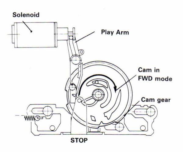
Figure 7

Figure 9
6. DISASEMBLY
6.1 REMOVING THE TOP COVER
Remove the four screws (1) and the screw (2) as shown in the figure.

6.3 REMOVING THE MAIN P.W. BOARD
Remove the four securing screws (5) as shown in the figure.

6.4 REMOVING THE MECHANISM
Remove the six securing screws (6) as shown in the figure.
6.2 REMOVING THE FRONT PANEL
After removing the top cover, remove the seven securing screws (3) and the screw (4) as shown in the figure.


7. ELECTRICAL ADJUSTMENTS
Precautions before Adjustment
- Before playing the test tape back, thoroughly demagnetize the heads, capstan and similar metal parts using an eraser as the test tape-recorded tone is easily erased.
- 2 Do not place the test tape on any measuring instrument
- Do not put the test tape near a place where the eraser is used.
- 4. Method of Demagnetization: Turn the eraser power switch on at a remote position far away from the heads. Bring the eraser close to the heads, capstan and other parts to be demagnetized, and move it up and down four or five times to demagnetize. Slowly separate the eraser far away from the parts, and turn the power switch off.
- Do not use any magnetize it from time to time in the course of each adjustment.
- Do not turn semi-fixed resistor more than needed.
- 7 Do not apply locking bond excssively.
ADJUSTMENT POINT (COMPONENT SIDE)

7.1 HEAD AZIMUTH ADJUSTMENT
- 1. Remove the cassette door lid
- 2. Set the TAPE SELECT switch to the NORM position.
- Play the 14 kHz signal of the test tape MTT-256, back. Adjust the head azimuth adjusting screw for maximum VTVM reading.
- 4. Adjust the left screw.
- 5. If the peak output reads of the right and left channels are different, set the screws to obtain the mechanical center between the peaks.
- After adjustment, repeat the playback and stop setting a few times to make certain of no head azimuth deviation. Then, lock the screws with bond.
Mode: Playback

7.2 TAPE SPEED ADJUSTMENT
Play the 3 kHz signal of the test type MTT-111, back. Adjust the tape speed adjusting resistor inside the motor (M071) for 2990 to 3010 Hz counter indication,
NOTE:
- If a strong shock of similar vibration is applied to the back after adjustment, make certain that the measured tape speed had not changed.
- 2. Be careful that the frequency counter may indicate a wrong value because of too low counter input level.
- 3. Before adjustment, allow for 30 seconds or more after depressing of the PLAY button.


7.3 PLAY BACK OUTPUT LEVEL AND METER ADJUSTMENTS
- 1. Play the test tape MTT-150, and adjust RJ47 (L), RJ48 (R), in the audio P.W board (PJ03) so that the playback output at TP5 (L), TP6 (R), Dolby NR circuits becomes 390 mV.
- In the above condition, adjust RX13 (L) and RX14 (R) in the PX03 meter P.W. board so that the meter reading is 0 dB ( Dg mark indicating point).
Mode: Playback

7.4 REC/PLAY FREQUENCY CHARACTERISTIC ADJUSTMENT/MEASUREMENT (NORMAL)
- Load the AC-212 test tape in the cassette holder, reduce the Dolby level by -22 dB using the attenuator, and record 1 kHz and 12.5 kHz on non-recorded portion. (DOLBY-C position)
- Adjust RL01 (L) and RL02 (R) in the PJ03 P.W. board so that 1 kHz and 12.5 kHz frequencies become 0 ±1.0 dB when the tape is played back after rewinding.
- After adjustment, record 1 kHz, 10 kHz and 12.5 kHz, and check that the playback level differences of those frequencies are as given below.
- With the DOLBY switch at position "B", record 1 kHz, 10 kHz and 12.5 kHz, and check that their playback level differences are as given below.
- With the DOLBY switch OFF, record 1 kHz, 10 kHz and 12.5 kHz, and check that their playback level differences are as given below.
- With DOLBY OFF, check that the L/R channel balance for 10 kHz is less than 3 dB.
NOTE:
When 1 kHz level difference in DOLBY-C mode is 1 dB or more compared to the monitor, adjust RK01 (L) and RK02 (R) for the REC LEVEL adjustment previously, so that the difference is within 1 dB.
7.5 REC/PLAY FREQUENCY CHARACTERISTIC ADJUSTMENT/MEASUREMENT (CrO.)
- Load the AC-512 test tape in the cassette holder, reduce the Dolby level by -22 dB using the attenuator, and record 1 kHz and 12.5 kHz on non-recorded portion. (DOLBY-C position)
- Adjust RL05 in the PJ03 P.W. board so that 1 kHz and 12.5 kHz frequencies become 0 ± 1.0 dB when the tape is played back after rewinding.
- After adjustment, record 1 kHz, 10 kHz and 12.5 kHz, and check that the playback level differences of those frequencies are as given below.
- With the DOLBY switch at position "B", record 1 kHz, 10 kHz and 12.5 kHz, and check that their playback level differences are as given below.
- With the DOLBY switch OFF, record 1 kHz, 10 kHz and 15 kHz, and check that their playback level differences are as given below.
- With DOLBY OFF, check that the L/R channel balance for 10 kHz is less than 3 dB.


7.6 REC/PLAY FREQUENCY CHARACTERISTIC ADJUSTMENT/MEASUREMENT (METAL)
- Load the AC-712 test tape in the cassette holder, reduce the Dolby level by -22 dB using the attenuator, and record 1 kHz and 12.5 kHz on non-recorded portion. (DOLBY-C position)
- Adjust RL06 in the PJ03 P.W. board so that 1 kHz and 12.5 kHz frequencies become 0 ± 1.0 dB when the tape is played back after rewinding.
- After adjustment, record 1 kHz, 10 kHz and 12.5 kHz, and check that their playback level differences of those frequencies are as given below.
- With the DOLBY switch at position "B", record 1 kHz, 10 kHz and 12.5 kHz, and check that their palyback level differences are as given below.
- With the DOLBY switch OFF, record 1 kHz, 10 kHz and 15 kHz, and check that their playback level differencies are as given below.
- With DOLBY OFF, check that the L/R channel balance for 10 kHz is less than 3 dB.
8. VOLTAGE CONVERSION
To convert the unit to a different power source voltage, change the position as illustrated in the drawing below.
CAUTION:
DISCONNECT POWER SUPPLY CORD FROM AC OUTLET BEFORE CONVERTING VOLTAGE. DO NOT DISASSEMBLE THE VOLTAGE SELECTOR ABSO-LUTELY.
VOLTAGE SELECTOR

(N, A) Version


NOTE ON SAFETY:
SYMBOL ▲ FIRE OR ELECTRICAL SHOCK HAZARD. ONLY ORIGINAL PARTS SHOULD BE USED TO RE-PLACE ANY PART MARKED WITH SYMBOL ▲. ANY OTHER COMPONENT SUBSTITUTION (OTHER THAN ORIGINAL TYPE), MAY INCREASE RISK OF FIRE OR ELECTRICAL SHOCK HAZARD.
9. BLOCK AND LEVEL DIAGRAM
PLAYBACK LEVEL DIAGRAM

REC. LEVEL DIAGRAM


16 MZ 1663


(PU 03) Power Supply/Logic Main P.W. Board
(P883) Power Transf. Connecitor P.W. Board


(PS 03) Logic Switch/LED indicator P.W. Board

(PX 03) FL Meter/Counter Driver P.W. Board

(PJ 43) Rec Volume P.W. Board

(PJ 33) NR Switch/MPX Switch P.W. Board
5500

(PG 03) Headphone
(PJ 23) Bias Fine Volume P.W. Board


Model SD-35


0,
0
J852
(P833) Power Switch P.W. Board
(P883) Power Switch

(PG 03) Headphone Jack P.W. Board

(P883) Power Transf. Connector P.W. Board (E Only)

al amonths an - 14-1200032000 120000
(PU 03) Power Supply/Logic Main P.W. Board
12. EXPLODED VIEWS AND PARTS LIST
[P01-99] FRONT PANEL AND ASSOCIATED MECHANISM FOR CASSETTE TAPE OPERATION

|
REF.
DESIG. |
PART NO. | DESCRIPTION |
REF.
DESIG. |
PART NO. | DESCRIPTION |
|---|---|---|---|---|---|
| 001B | 4822 426 51188 | Front Panel, (Black) [N, E] | 001C | 4822 535 91993 | Pin, Eject; (Black) [N, E] |
| 4822 426 51187 | Front Panel, (Gold) [E] | 4822 535 91994 | Pin, Eject; (Gold) [E] | ||
| 004B | 4822 454 11825 | Badge | 004C | 4822 492 51692 | Spring, Eject |
| 007B | 4822 410 24643 | Button, Select; (Black) [N, E] | 005C | 4822 532 11295 | RG Ring, E Type Ø3 |
| 4822 410 24639 | Button, Select; (Gold) [E] | 006C | 4822 454 11914 | Escutcheon, Mecha | |
| 008B | 4822 403 20219 | Joint, Select Button | 007C | 4822 290 30276 | Lug |
| 009B | 4822 410 24515 | Button, Eject; (Black) [N, E] | 010C | 4822 403 53072 | Hook, Cassette Case |
| 4822 410 24511 | Button, Eject; (Gold) [E] | 011C | 4822 492 63414 | Leaf Spring | |
| 015B |
4822 454 11481
4822 454 11478 |
Escutcheon, Cassette; (Black) [N, E]
Escutcheon, Cassette; (Gold) [E] |
012C
014C |
4822 532 11295
4822 492 32672 |
RG Ring, E Type Ø3
Spring |
| 0178 | 4822 450 60925 | Window Cassette Case | 0150 | 4822 403 20218 | Bracket (K) Mecha: Left |
| 0198 | 4822 403 53152 | Retainer Cassette Case | 0220 | 4822 492 41643 | Spring Door Open |
| 0208 | 4822 459 80375 | Bushing FL (L) | 0230 | 4822 492 41644 | Spring, Cassette Open |
| 021B | 4822 459 80376 | Bushing, FL (B) | 0300 | 4822 459 20391 | Door Assembly |
| 031B | 4822 410 25601 | Button Mecha: (Black) [N E] | 0310 | 4822 464 50528 | Dumper |
| 4822 410 25779 | Button Mecha: (Gold) [E] | 0320 | 4822 502 12557 | Screw | |
| 032B | 4822 535 71094 | Pin Mecha Button | 0330 | 4822 532 11443 | Betainer Mecha: Bight |
| 0368 | 4822 410 25602 | Button Select: (Black) [N E] | 0350 | 4922 466 30178 | Shield Mecha Head |
| 0300 | 4822 410 25002 | Button, Select; (Gold) [E] | 0390 | 4022 400 30170 | TI Washer OR |
| 0200 | 4022 410 25/01 | Bin Select Rutton | 0300 | 4022 532 11300 | T.L. Washer, OR |
| USOB | 4022 535 / 1094 | Fin, Select Button | 0014 | 4000 400 41007 | Changes Usedahang lask |
| 0470 | 4922 450 20255 | Window Laval | 921K | 4822 462 41037 | Stopper, Headphone Jack |
| 0478 | 4822 459 20355 | 9416 | 4822 403 52845 | Shield, Volume | |
| 0496 | 4022 409 40000 | Lodiestor Level (Pleak) [N E] | 4000 404 50074 | March | |
| 0518 | 4822 404 20004 | Indicator, Level; (Black) [N, E] | A001 | 4822 464 506/1 | Mechanism Assembly |
| 0500 | 4822 454 20098 | Kach Bas Level; (Gold) [E] | and the second second | ||
| 0528 | 4822 412 20091 | Knob, Rec Level; (Black) [N, E] | |||
| OFAD | 4822 412 20092 | Rhob, Rec Level; (Gold/ [E] | 1220 | ||
| 0548 | 4822 466 61567 | Butter, Function Lens | and the second | and the second se | |
| 0558 | 4822 412 20091 | Knob, Rec Barance; (Black) [N, E] | ALC: NO | and the second second | Note of the second s |
| 4822 412 20092 | Knob, Hec Barance; (Gold) [E] | and share the | 1012 State | A THE REPORT OF A DESCRIPTION OF A DESCRIPANTE A DESCRIPTION OF A DESCRIPTION OF | |
| 056B | 4822 381 10795 | Lens, Mecha Function | C. I. A.S.C. Georgia . 13 | ||
| 3 | |||||
| 05/B | 4822 443 509/6 | Chassis, Front (Black) [N, E] | |||
| 058B | 4822 443 50976 | Chassis, Front (Gold) [E] | March 1 | ||
| 059B | 4822 443 40295 | Escutcheon, Cap (R); (Gold) [E] | COMPANY AND A STORE OF A STORE | ||
| 060B | 4822 443 40294 | Escutcheon, Cap (L); (Gold) [E] | |||
| 070B | 4822 412 20999 | Knob, Bias | topage assessments | ||
| 1 | 1 | 이번요 잘 다 많이 안 한 것이 많이 | |||
| 2 11 3000 PM | |||||
| The second s | 날개도 잘 못 한 것은 그렇게 하는 것이다. | ||||
| hand is | |||||
| The part asserts and the second second | and in the | 1000 | |||
| 1 Star Star | |||||
| 11 12 | |||||
| 1. | |||||
| 1923 | 1 | ||||
| 1 | |||||
| es. Mines were in Children and a line of | 11.1 | ||||
| 1 | 이 제 그는 것이라도 그의 안전 것같이 ? | ||||
| 1 1 | |||||
| 1 1 | |||||
| 1 | |||||
| 1 | The second s | ||||
| 100 | |||||
| 1.19 | |||||
| and the second | |||||
| 101111 | |||||


|
REF.
DESIG. |
PART NO. | DESCRIPTION |
|---|---|---|
|
001B
061B 071B 072B 076B 077B 081B 083B |
4822 426 51186
4822 443 51015 4822 256 91204 4822 454 20702 4822 256 91205 4822 256 91206 4822 412 20989 4822 412 20157 |
Front Panel Assembly
Cover, Cassette Case Holder Indicator, FL Holder, FL Holder, LED Knob, Rec Volume Knob, Balance/Bias |
|
001C
003C 006C 010C 011C 012C 014C 015C 022C 023C |
4822 349 50309
4822 358 30519 4822 454 11914 4822 403 53072 4822 492 63414 4822 532 11295 4822 492 32672 4822 403 20218 4822 492 41643 4822 492 41644 |
Counter, Tape
Belt, Counter Escutcheon, Mecha Hook, Cassette Case Lock Leaf Spring RG Ring, E Type Ø3 Spring Bracket (K), Mecha Spring, Door Open Spring, Cassette Open |
|
030C
031C 032C 033C 035C 038C 041C 042C |
4822 459 20391
4822 464 50528 4822 502 12557 4822 532 11443 4822 466 30178 4822 532 11388 4822 290 30266 4822 290 30266 |
Door Assembly, Cassette
Dumper Screw, Dumper Retainer (R) Mecha Shield, Mecha Head T.L. Washer, OR Lug Lug |
| AUUT | 4822 464 50671 | Mechanism Assembly |
[P02-99] LID (TOP & BOTTOM COVER), REAL PANEL, GENERAL PARTS AND PACKING MATERIALS

|
REF.
DESIG. |
PART NO. | DESCRIPTION |
REF.
DESIG. |
PART NO. | DESCRIPTION |
|---|---|---|---|---|---|
|
051B
052B |
4822 410 24635
4822 278 80239 |
Button, Power
Link, Power Button |
001S | 4822 600 70468 |
PACKING
Packing Case [N] |
| 041C | 4822 290 30266 | Lug | 0025 | 4822 600 70464 | Cushion |
|
001D
006D |
4822 426 40366
4822 501 11008 |
Lid, Top Cover
B.T. Screw B4 x 8 |
0005 |
4822 600 70347
4822 736 13572 |
User Manual |
| 001G | 4822 464 70419 | Chaesis (1) | 004T | 4822 600 70363 | Polyethylene Bag |
| 011G | 4822 403 53074 | Bracket, Transformer | J011 | 4822 265 10092 | Jack, AC Adaptor [E] |
| 014G | 4822 454 11298 | Shield, Transformer | W011 | 4822 321 21438 | Connective Cord BCA |
| 021G | 4822 464 70418 | Chassis (R) | ▲W015 | 4822 321 21123 | A.C. Power Cord, [N] |
| 026G | 4822 403 53073 | Stay, Center | 63 | 100 | |
| 029G | 4822 290 30266 |
Lug
Elat Washer, I |
0500 | and an and a second and | |
| 041G | 4822 426 60516 | Lid. Bottom Cover | 6.1 | ||
| 046G | 4822 462 71361 | Leg | 08007106711-1 | ||
| 901G | 4822 426 20113 | Bear Papel [N] | 1000 | ||
| 5010 | 4822 426 20114 | Rear Panel [E] | 2000 | ||
| 908G | 4822 532 51314 | Bushing, AC Power Cord [E] | 5 28 19 | ||
| 990G | 4822 600 70229 | Label, Caution | |||
| ∆ J093 | 4822 265 20222 | Plug, AC Inlet [N] | |||
| ∆ L801 |
4822 148 60167
4822 148 80744 |
Power Transformer [N]
Power Transformer [E] |
|||
| ∆ SO93 |
4822 272 10235
4822 272 10236 |
Voltage Selector [E]
Voltage Selector [N] |
|||
| ∆ W001 | 4822 321 10429 | A.C. Power Cord [E] | 1632 | ||
|
801K
802K |
4822 255 40532
4822 255 40532 |
Heatsink
Heatsink |
|||
| and a second a second sec | Carl | ||||
| and the second | 1 0 | 926 | |||
| a la come de | |||||
| 2 | |||||
| and a second | |||||
| de ser a | 12 | ||||
| Solar States | Sec. 1 | ||||
| 124 | |||||
| ALL | 1.10 | ||||
| 1 60 | 188 | ||||
| 24.20 | A Baral | ||||
| 1 | 1 18 | 19 11 | |||
| 1 1 | |||||
| and the set of the set | 1 | ||||
| and the second | |||||
| The start | A | ||||
| 1 | |||||
| 1 | |||||
| and the second second | 6280 | ||||
| - State | a come court and | ||||
(P03-99) PARTS ASSEMBLED ON THE TOP AND REVERSE OF CHASSIS

Model SD-45II /SD-35
13. ELECTRICAL PARTS LIST
| ASSIGNMENT OF COMMON PARTS CODES. |
REF.
DESIG. |
PART NO. | DESCRIP | TION |
REF.
DESIG. |
PART NO. | DESCRIPTION |
REF.
DESIG. |
PART NO. | C | DESCRIPTION | ||
|---|---|---|---|---|---|---|---|---|---|---|---|---|---|
| R •••• : (1) GD05 140, Carbon film fixed resistor, ±5%, 1/4W | Receiver ion | 2 | 598 | That Age | 1999 - | ||||||||
| R . (2) GD05 160, Carbon film fixed resistor, ±5%, 1/600 | - | PG03-HEA | DPHONE | JACK | PJ03-SEM | ICONDUCTORS | PJ23-BIAS | FINE VOLUME | |||||
| (I) — Resistance value | 0001 | 4922 122 40401 | CIRCUIT | BOARD IS | SD-45MK11/SD-35 | DK11 | 4822 130 33305 | Diode | 155133, etc. | BI 11 | 4822 100 20613 | CIRCUIT E | SOARD [SD-45MKII] |
| Examples | JG01 | 4822 267 30617 | Jack, Head | ap. 0.022 | lack) [N, E] | DS46 | 4822 130 33305 | Diode | 1SS133, etc. | 4022 100 20010 | variable rie | ||
| Resistance value | 4822 264 10132 | Jack, Head | dphone; (G | iold) (SD-45MKII) | DS61 | 4822 130 33305 | Diode | 1SS133, etc. | WL90 | 4822 323 10081 | Jumper Lea | nd, 3P | |
|
0.1Ω001 10Ω100 1kΩ102 100kΩ104
0.50 005 180 180 2.7k0 272 680k0 684 |
I WCOO | 4000 000 10001 | [E] | ad 20 (ST | DY04 | 4822 130 80273 | Zener | 8.2V [SD-35] | 2418 | DI22 BIAS | |||
| 1Ω010 100Ω101 10kΩ103 1MkΩ105 | WG90 | 4822 323 10081 | Jumper Le |
ad, SF [SL
ad, 3P [SL |
D-35] | 0601 | 4822 209 83614 | IC | TEA0665 | 1. 1 | CIRCUIT E | OARD [SD-35] | |
| 6.8Ω068 390Ω391 22kΩ223 4.7MkΩ475 | and states | 52403 | 100894 11 40772 4014 | Q602 | 4822 209 83614 | IC | TEA 0665 | RL11 | 4822 100 20613 | Variable Re | esistor 10KΩ(B), Bias | ||
| (Note) Please distinguish 1/4W from 1/6W by the shape of parts | 2010 | 4822 492 | Q631 | 4822 209 80401 | IC | NJM4558D | RV02 | 4822 100 20615 | Variable Re | esistor 250KΩ(W), Rec | ||||
| used actually. | CIRCUIT | BOARD | SD-45MKII/SD-35] | 0651 | 4822 130 42483 | Transistor |
2SC536SP(F, G), etc.
2SC536SP(F, G), etc. |
WI 90 | 4822 323 10107 | Jumper Lea | ad 3P | ||
| 0 | 4002 | 1022 100 12100 | 1022 020 10101 | ||||||||||
| (1) DD1 | The second | 101 T 101 101 10 | QG21 | 4822 209 80401 | IC | NJM4558D | Strange Co | ||||||
| 0617 | 1022 124 11199 | PJ03-CAP | 0 68 F | 50V | 0121 | 4922 200 91565 | IC | NUM2041DD | PJ33-DOLE | SY NR/MPX FILTER | |||
| C618 | 4822 124 41188 | Elect | 0.68µF | 50V | 0,141 | 4822 209 81505 | Transistor | 2SC536SP(F, G), etc. | CV01 | 4822 122 32486 | Ceramic Ca | p. 0.01µF +80% -20%[E] | |
| Capacity value | C627 | 4822 124 41188 | Elect | 0.68µF | 50V | QJ42 | 4822 130 42483 | Transistor | 2SC536SP(F, G), etc. | ||||
| Tolerance | C628 | 4822 124 41188 | Elect | 0.68µF | 50V | QJ48 | 4822 130 42483 | Transistor | 2SC536SP(F, G), etc. | SS04 | 4822 276 11944 | Push Switc | h, NR ON/OFF |
| Examples | C631 | 4822 124 22039 | Elect | 220µF |
16V
16V |
OKOL | 4922 200 20270 | 10 | TDD1601 | SS05 | 4822 276 11944 | Push Switch | |
| ① Tolerance (Capacity deviation) | C632 | 4822 124 22039 | Elect | 220µF | 100 | QK11 | 4822 209 70379 | Transistor | 2SC536SP(F, G), etc. | 5506 | 4822 276 11944 | Push Switch | n, MPX UN/OFF |
| ±0.25pF0 | CG23 | 4822 122 40491 | Ceramic | 0.022µF | +80% -20% | QK12 | 4822 130 42483 | Transistor | 2SC536SP(F, G), etc. | W691 | 4822 323 10129 | Jumper Lea | ad, 6P |
|
±0.5pr1
±5%5 |
QK13 | 4822 130 42715 | Transistor | 2SA608SP(F, G), etc. | and the second | 14 | |||||||
| * Tolerance of COMMON PARTS handled here are as follows: | CJ31 | 4822 121 43005 | Film | 820pF | ±5% | QK14 | 4822 130 42483 | Transistor | 2SC536SP(F, G), etc. | a state of the | |||
| 0.5pF ~ 5pF±0.25pF | CJ32 | 4822 121 43005 | Film | 820pF | 10V | OK 16 | 4822 130 42483 | Transistor | 2SC536SP(F, G), etc. | MESSEA. | PJ43-REC | ||
| 12pF ~ 560pF±5% | CJ41 | 4822 124 90363 | Elect | 220µF | 10V | QK17 | 4822 130 42483 | Transistor | 2SC536SP(F, G), etc. | RV01 | 4822 100 20272 | Variable Re | esistor, 100KΩ(A) |
| ② Capacity value | CJ43 | 4822 124 90357 | Elect | 2.2µF | 50V | RV02 | 4822 100 20583 | Variable Re | esistor, 250KΩ(B) | ||||
| 0.5pF005 3pF030 100pF101 | CJ44 | 4822 124 90357 | Elect | 2.2µF | 50V | QL01 | 4822 209 70378 | IC | TDA1600 | ||||
| 1.5pF015 47pF470 560pF561 | CJ45 | 4822 124 90371 | Elect | 470µF | 100 | 0525 | 4822 130 42483 | Transistor | 2SC536SP(F_G) etc | WE90 | 4822 323 10198 | Jumper Lea | ad, 6P |
| CJ40 | 4022 124 90371 | LIECT | 4700 | Q$31 | 4822 130 42483 | Transistor | 2SC536SD(F, G), etc. | PJ43-REC | VOLUME | ||||
| (1) DK16300 High dielectric constant ceramic condenser | CK11 | 4822 122 32486 | Ceramic | 0.01µF | +80% -20% | [SD-45MK | (11) | CIRCUIT | BOARD [SD-35] | ||||
| Disc type | 0.01 | 4000 101 40701 | Film | 4700-E | += 9/ | 01/11 | 4922 120 42125 | Transistor | 25D1302(S T) | RV01 | 4822 100 20272 | Variable Re | esistor 100KΩ(A) |
| Temp. chara. 2B4, 50V | CL01 | 4822 121 42791 | Film | 4700pF |
15%
+5% |
OW12 | 4822 130 42125 | Transistor | 2SD1302(S, T) | WEGO | 4822 323 10146 | lumper Le | ad 6P |
| Capacity value | CL03 | 4822 121 42344 | Film | 220pF | ±5% | QW13 | 4822 130 42483 | Transistor | 2SC536SP(F, G), etc. | WE91 | 4822 323 10086 | Jumper Lea | ad, 4P |
| CL21 | 4822 122 32486 | Ceramic | 0.01µF | +80% -20% | QW14 | 4822 130 42483 | Transistor | 2SC536SP(F, G), etc. | in the second | A Contraction | |||
| Example | CL22 | 4822 122 32486 | Ceramic | 0.01µF | +80% -20% | Sector Sector | D IO2 MICO | 0002100 | C SW/INDICATOR | ||||
| 100pF101 1000pF102 10000pF103 | CW01 | 4822 122 40491 | Ceramic | 0.022µF | +80% -20% | 1691 | 4822 265 10063 | Jack, 6P [ | SD-45MKII] | CIRCUIT E | BOARD [SD-45MKII] | ||
| 470pF471 2200pF222 | CW05 | 4822 124 22274 | Elect | 4.7µF | 50V | 4822 265 10105 | Jack, 4P [ | SD-35] | DS21 | 4822 130 33305 | Diode | 1SS133, etc. | |
| CW06 | 4822 124 22274 | Elect | 4.7µF | 50V | JE90 | 4822 265 10063 | Jack, 6P | DS23 | 1 1 Dec. | ||||
| (1) EA 10, Electrolytic condenser | CW07 | 4822 124 22274 | Elect | 4.7µF | 50V | JG90 | 4822 265 10062 | Jack, 3P [ | SD-35] | 2 | 4822 130 33305 | Diode | 1SS133, etc. |
| One-way lead type, Tolerance ±20% | CW08 | 4822 124 22274 | Elect | 4.7µF | 50V | 1190 | 4822 265 30473 | Jack 9P | A CONTRACT OF A | DS36 | 4822 130 33305 | Diode | 1SS133 etc. |
| CW12 | 4822 124 22274 | Elect | 4.7µF | 50V | JL01 | 4822 265 10078 | Plug, 3P | DS41 | 4822 130 33305 | Diode | 1SS133, etc. | ||
| Capacity value | CW13 | 4822 122 40491 | Ceramic | 0.022µF | +80% -20% | JL90 | 4822 265 10062 | Jack, 3P [ | SD-35] | DY21 | 4822 130 32179 | L.E.D. | SLP981C |
| ISTORS | JW01 | 4822 265 30397 | Terminal, | 4P; RCA | DY23 | 4822 130 33203 | L.E.D. | SLP481C | |||||
| ① Capacity value | RJ47 | 4822 100 11041 | 10KΩ. | Trimming | 1X92 | 4822 265 10064 | Jack, 7P [ | SD-45MINIT | DY41 | 4822 130 32181 | L.E.D. | SLP281F | |
| 0.1μF104 4.7μF475 100μF107 | RJ48 | 4822 100 11041 | 10KΩ , | Trimming | QS52 | 4822 130 42715 | Transistor | 2SA608SP(F, G), etc. | |||||
| 0.33μF334 10μF106 330μF337 | L601 | 4822 157 52461 | M.P.X. Co | il, 19KHz | Q$53 | 4822 130 42715 | Transistor | 2SA608SP(F, G), etc. | |||||
| 1μ | RK01 | 4822 100 20545 | 22KΩ, | Trimming | L602 | 4822 157 52461 | M.P.X. Co | il, 19KHz | Q$54 | 4822 130 42483 | Transistor | 2SC536SP(F, G), etc. | |
| Working voltage | 4822 100 20343 | 22136, | in | L603 | 4822 156 10842 | Choke Coi | 1, 36mH | C. Seren - County | S | ||||
|
6.3V006 25V025
10V 010 35V 035 |
RL01 | 4822 100 11042 | 47KΩ, | Trimming | LK01 | 4822 152 20564 | Choke Coi | I, 22mH | M12 | ||||
| 16V016 50V050 | RL02 | 4822 100 11042 | 47KΩ, | Trimming | LK02 | 4822 152 20564 | Choke Coi | I, 22mH | 05446 | ||||
| RL05 | 4822 100 20545 |
22KΩ,
22KΩ |
Trimming | 4822 146 10184 | OSC Trans | tormer | |||||||
|
(2) DF15 350, Plastic film condenser
One-way type, Mylar +5% 50V |
I NLOO | 4622 100 20545 | 22136, | Training | 4022 132 20022 | CHOKE CO | 1, 2.21111 | ||||||
| 0 | XK01 | 4822 242 71533 | Ceramic V | ibrator, CSB500E | |||||||||
| Capacity value | Carlos - | 1.100 | |||||||||||
| Examples | ET IN | 19 8 | |||||||||||
| ① Capacity value | 1 1 20 1 | 3. | Set ogen | 1 | |||||||||
|
0.001μF (1000pF)102 0.1μF104
0.0018μF |
and a start Day | The second second | 675 | ||||||||||
| 0.01µF103 1µF105 | - | 1 | 2014 | C. CEA | |||||||||
| 0.015µF153 | 1 setting | AND A CONTRACT | ALL STRAFT | A State | |||||||||
| A REAL PROPERTY AND A REAL PROPERTY AND A REAL PROPERTY. | and the second | and the second se | The second se |
EARS AN INTERNET ASSESSED ON THE YOF AND REPERTSE OF REACH
|
REF.
DESIG. |
PART NO. | DESCRIPTION |
REF.
DESIG. |
PART NO. | DESCRIPTION |
|---|---|---|---|---|---|
| SS21 | 4822 276 11559 | Push Switch, Rec | ₫ D801 | 4822 130 32816 | Diode 1SR35-200A |
| 5523 | 4922 276 11550 | Buch Switch Bac | 1 0000 | 4822 130 50314 | Diode RB-152 (SD-35) [N] |
| 5022 | 4022 270 11559 | Fush Switch, Nec | A D802 | 4822 130 32810 | Diode ISR35-200A |
| 5527 | 4822 276 11550 | Push Switch Memory | 1 0803 | 4022 130 32010 | Diode 15R35-200A [5D-45MK11] |
| 5530 | 4822 276 11559 | Push Switch, Memory | 1 0804 | 4022 130 32010 | Diode ISR35-200A [SD-45WKT] |
| 5557 | 4822 276 11559 | Push Switch, Play | 4022 130 32500 | Diode DSF10C, etc. | |
| 0041 | 4022 270 11000 | i usir ovriteri, i ruy | 1 0800 | 4022 130 32500 | Diode DSF10C, etc. |
| WY02 | 4822 323 10272 | Jumper Lead, 8P | 1 0810 | 4022 130 32500 | Diode DSF10C, etc. |
| WY03 | 4822 323 10272 | Jumper Lead, 8P | 1 0811 | 4822 130 33305 | Zoper BD15 B1 (SD 45MK11) |
| ▲ D812 | 4822 130 33759 | Zener RD4.7JB2 [SD-45MK11] | |||
| 1. | CIRCUIT POARD (SD 25) | BRIDTRIZI | R-EDXA | ||
| 3022 | 4922 276 12210 | Push Switch NR ON/OFF | QM01 | 4822 130 60174 | Transistor 2SD1379 |
| 3022 | 4822 276 12219 | Push Switch NB B/C | QM02 | 4822 130 60174 | Transistor 2SD1379 |
| $$12 | 4822 276 12219 | Push Switch MPX Filter | QM31 | 4822 130 42483 | Transistor 25C5365P(F, G), etc. |
| 0012 | 4022 270 12210 | 01/132 | 4822 130 42483 | Transistor 25C5365P(F, G), etc. | |
| W691 | 4822 323 10087 | Jumper Lead, 4P | 01433 | 4822 130 42483 | Transistor 2505365P(F, G), etc. |
| WS03 | 4822 323 10087 | Jumper Lead 4P | 01434 | 4822 130 42483 | I ransistor 25C5365P(F, G), etc. |
| 4022 209 02009 | |||||
| BET REDUCT TRUTTER SERVICE | 4022 130 42/15 | Transistor 25A0085P(F, G), etc. | |||
| PU03-LOGIC MAIN | 4822 130 42483 | Transistor 25C5365P(F, G), etc. | |||
| CIRCUIT BOARD [SD-45MKII/SD-35] | 211/184 | 4822 130 42483 | [SD-45MKII] | ||
| ni minut i fibio pri State - to si | QU01 | 4822 209 83812 | IC LM640202A | ||
| PU03-CAPACITORS | QU20 | 4822 130 42715 | Transistor 2SA608SP(F, G), etc. | ||
| CM81 | 4822 122 40491 | Ceramic 0.022µF +80% -20% | QU21 | 4822 130 42483 | Transistor 2SC536SP(F, G), etc. |
| CM82 | 4822 122 32486 | Ceramic 0.01µF +80% -20% | QU51 | 4822 130 42483 | Transistor 2SC536SP(F, G), etc. |
| 0040 | R Tautan in Links | QU54 | 4822 130 42483 | Transistor 2SC536SP(F, G), etc. | |
| CU04 | 4822 122 32486 | Ceramic 0.01µF +80% -20% | QU55 | 4822 130 42715 | Transistor 2SA608SP(F, G), etc. |
| CU21 | 4822 122 32486 | Ceramic 0.01µF +80% -20% | QU56 | 4822 130 42483 | Transistor 2SC536SP(F, G), etc. |
| QU57 | 4822 130 42483 | Transistor 2SC536SP(F, G), etc. | |||
| C801 | 4822 124 41313 | Elect 1000µF 35V | QU62 | 4822 130 42483 | Transistor 2SC536SP(F, G), etc. |
| C806 | 4822 124 22267 | Elect 220µF 16V | QU71 | 4822 130 30857 | IC BA222 |
| C809 | 4822 122 32486 | Ceramic 0.01µF +80% -20% | ASCHART | 1 OF FREEDOM COM | |
| C810 | 4822 122 32486 | Ceramic 0.01µF +80% -20% | QU72 | 4822 130 42715 | Transistor 2SA608SP(F, G), etc. |
| THE OF ORMO | R TRIDUCE | QU73 | 4822 130 42483 | Transistor 2SC536SP(F, G), etc. | |
| PU03-RESISTORS | QU92 | 4822 130 42483 | Transistor 2SC536SP(F, G), etc. | ||
| GU03 | 4822 111 91276 | 10KΩx6 ±5% 1/5W, Allay | QU93 | 4822 130 42483 | Transistor 2SC536SP(F, G), etc. |
| A R801 | 4822 116 60309 | 2.2Ω ±5% ¼W, Fusible | QU94 | 4822 130 42483 | Transistor 2SC536SP(F, G), etc. |
| [SD-45MKII] | Q801 | 4822 209 83821 | IC NJM78M06A | ||
| A R802 | 4822 111 90724 | 330Ω ±5% ½W [SD-45MKII] | 0802 | 4822 209 82829 | IC NJM78M15A |
| A R805 | 4822 116 60307 | 1Ω ±5% ¼W, Fusible | Q803 | 4822 130 60496 | Transistor 2SB891(Q, R) |
| AR806 | 4822 116 60306 | 1Ω ±5% ½W, Fusible | [SD-45MK11] | ||
| [SD-45MKII] | |||||
| AR807 | 4822 116 21086 | 1Ω ±5% ½W, Fusible | 200 TRIP | PU03-MISCELLANEOUS | |
| JU90 | 4822 265 40602 | Plug, 9P | |||
| PU03-SEMICONDUCTORS | JU92 | 4822 265 10062 | Jack, 3P [SD-45MK11] | ||
| DM01 | 4822 130 32508 | Diode DSF10C, etc. | JU93 | 4822 265 10062 | Jack, 3P [SD-35] |
| DM02 | 4822 130 32508 | Diode DSF10C, etc. | 4822 265 10063 | Jack, 6P [SD-45MK11] | |
| DM31 | 4822 130 33759 | Zener RD4.7JB2 | saorouoxobhi | 12.0004 | |
| DM81 | 4822 130 33758 | Zener RD4.7JB2 | JY02 | 4822 265 10059 | Jack, 8P |
| JY03 | 4822 265 10059 | Jack, 8P [SD-45MK11] | |||
| DU06 | 4822 130 33305 | Diode 1SS133, etc. | 4822 265 10105 | Jack, 4P [SD-35] | |
| DU11 | 4822 130 33305 | Diode 1SS133, etc. | |||
| DU20 | 4822 130 33305 | Diode 188133 etc. | WM91 | 4822 323 10135 | Jumper Lead, 7P |
| DU21 | 4822 130 33305 | Diode 188133, etc. | WM92 | 4822 323 10113 | Jumper Lead, 5P |
| DU22 | 4822 130 33305 | Diode 188133, etc. | WM93 | 4822 323 10077 | Jumper Lead, 3P |
| 0051 | 4822 130 33759 | Diada 188400 and | W801 | 4822 323 10057 | Jumper Lead, 6P |
| 0052 | 4822 130 33305 | Diode 155133, etc. | The second second | O TOT ASTONOLISTED COMPANY | |
| DU53 | 4822 130 33305 | Diode 155133, etc. [SD-45MK11] | XU01 | 4822 242 71405 | Ceramic Vibrator, CSG800K |
| DU65 | 4822 130 33305 | Diode 155133, etc. | GROCTJ | Covor 1 450 test 60026 LEE 0 | |
| DU66 | 4822 130 33305 | Diode 15S133, etc. | 1.4 | 8305T. | 0.9.3 (000000000000000000000000000000000000 |
| DUZI | 4822 120 22205 | Diode 199122 etc | 1 DOGET J | E DY 21 - 6822 610 80326 - 1. E O | |
| DUOG | 4022 130 33305 | Diode 199133, etc. | 0 | 1.7.31311 | 0 Y23 1 4022 130 80226 1 L 4 0 |
| 0090 | 4822 130 33305 | Diode 199133 etc. | 0 | L TIGSE | 0.0.0.0 SECON 001 1388 171/101 |
| DU97 | 4822 130 33305 | Diode 1SS133 etc | LA . | ||
| 5090 | 1022 100 30300 | 2.000 100100, 610. | 9 | ||
| TO THE PARTY OF THE | the second |
Model SD-45II / SD-35
|
REF.
DESIG. |
PART NO. | DESCRIPTION |
ner.
District |
REF.
DESIG. |
PART NO. | ESCRIPTION | |
|---|---|---|---|---|---|---|---|
| Interio | the state of | odder Briterick rei | |||||
| 1.199 | PX03-FL METER/COUNTE | :R | QS52 | 4822 130 42715 | Transistor | 2SA608SP(F, G), etc. | |
| DRIVER CIRCUIT BOARD | QS53 | 4822 130 42715 | Transistor | 2SA608SP(F, G), etc. | |||
| 1104485 | [SD-45MKII] | Long | QS54 | 4822 130 42483 | Transistor | 2SC536SP(F, G), etc. | |
| HOMBS | (822-130-32819 | Doon - | 1080.4 | QX01 | 4822 209 70049 | IC | BA6146 | |
| PX03-CAPACITORS | 1080.5 | QX02 | 4822 209 70049 | IC | BA6146 | ||
| CX15 | 4822 122 40491 | Ceramic 0.022µF +80% | -20% | ||||
| CX16 | 4822 122 40491 | Ceramic 0.022µF +80% | -20% | PX03-MISC | ELLANEOUS | ||
| CX17 | 4822 122 32486 | Ceramic 0.01µF +80% | -20% | SS21 | 4822 276 11559 | Push Switch | , Rec |
| CX32 | 5322 122 31626 | Ceramic 100pF ±5% | 1 343 | SS23 | |||
| Terra - unitalization sizon | 1.2100.0 | 1 | 4822 276 11559 | Push Switch | , Rec | ||
| PX03-RESISTORS | 100000 | SS27 | |||||
| RX13 | 4822 100 20545 | 22KΩ, Trimming | COLUMN | SS41 | 4822 276 11559 | Push Switch | i, Play |
| RX14 | 4822 100 20545 | 22KΩ, Trimming | TENKS . | 1 | 4000 400 00404 | D: 1 | BISCHARTS 276 12210 |
| RX19 | 4822 111 90727 | 22012 ±5% ½W | CARSE | 4822 130 90434 | Display Uni | ers | 4822 276 12219 | |
| GX01 | 4822 111 90956 | 100K Ox8 Allav | DAMO | WU93 | 4822 323 10224 | Jumper Lea | d 3P |
| GX02 | 4822 111 90608 | 100K 0x12 Allay | NEMO. | WX92 | 4822 323 10113 | Jumper Lea | d 5P |
| GAUL | 4022 111 00000 | roonser 12, runay | 1 Shoto | WY02 | 4822 323 10136 | Jumper Lea | d 8P |
| < 2SADOSSATE, G | PX03-SEMICONDUCTORS | 1-587AD | WY03 | 4822 323 10087 | Jumper Lea | d. 4P | |
| DX01 | 4822 130 33305 | Diode 1SS133. etc. | and the second | ||||
| DX02 | 4822 130 80115 | Zener RD15JB1 | in the second | C. Physical Contract of the | |||
| DX03 | 4822 130 80116 | Zener 24V | 1 Copression | Contraction of the Contract | PX13-FL M | ETER | |
| DX05 | 4822 130 33759 | Zener RD4.7JB2 | CIRCUIT B | OARD [SD-45MKII] | |||
| DX06 | 4822 130 33305 | Diode 1SS133, etc. | VX01 | 4822 130 90401 | Display Uni | t | |
| DX07 | 4822 130 33305 | Diode 1SS133, etc. | 1 | ALL STORE STORE | |||
| DX11 | 4822 130 32508 | Diode DSF10C, etc. | 1 1200 | 1 | C. STRA RUIN | ||
| DX32 | 4822 130 33305 | Diode 1SS133, etc. | 1 | 5- X06+ Turb.6 | P833-POWE | ||
| 0201 | 4822 130 60494 | Transistor 28052680/E | G) ata | 1 0951 | 4822 122 40305 | Coromic Cor | |
| 0004 | 4822 130 42483 | Transistor 250505F(F, | G) etc. | 120001 | 4022 122 40305 | Cerannic Ca | 5. 0.01µF 400V |
| QX05 | 4822 130 42715 | Transistor 2SA608SP(F. | G), etc. | A $851 | 4822 276 11141 | Push Switch | Power |
| QX06 | 4822 130 42715 | Transistor 2SA608SP(F. | G), etc. | er Audes | 1051 [ 4822 124 1220 ] | ||
| QX31 | 4822 209 83731 | IC TM4028A | C- 8081 - 3410.0 | ||||
| QX32 | 4822 130 60497 | Transistor 2SC3311A(Q, | R) | 0.0127 | P883-PT 2N | ID CONNECT | |
| 1004 | 1000 005 10000 | CIRCUIT B | OARD [SD-35] | ||||
| MILION | 4000 000 10077 | PX03-MISCELLANEOUS | J801 | 4822 265 10063 | Jack, 6P | ||
| WI 193 | 4822 323 10077 | Jumper Lead, SP | |||||
| WX91 | 4822 323 10050 | Jumper Lead, 7P | Intel Work State | ||||
| A BOMBS MUN | 4922 209 80827 | NO | - Louise | an owner were bound | ||||
|
, PERMANANA
250891 (C. P.I. XIII) |
PX03-FL METER/KEY SW
CIRCUIT BOARD [SD-35] |
/LED |
site
site |
and with a state | |||
| and the second second | and and seas | ||||||
| - anotary mark | PX03-RESISTORS | ||||||
| RX01 | 4822 100 11042 | 47KΩ, Trimming | 2norbuowee | ||||
| RX02 | 4822 100 11042 | 47KΩ, Trimming | DSF 105, 461 | ||||
| RX11 | 4822 116 60444 | 1802 ±5% 1/6W | , Metal [E] | OSF 100, etc. | Diode | ||
| PX03-SEMICONDUCTORS | PD4.7382 | Zározy | |||||
| DS21 | 4822 130 33305 | Diode 1SS133, etc. | 1 SOME | RD4.3182 | Sansi | ||
| DS23 | The state of the second state of the | Same and and an | - in should be | ||||
| 2 | 4822 130 33305 | Diode 1SS133, etc. | DARKS OCH AVEN. J. M. H. | ||||
| DS27 | 1000 100 00005 | Diada 100122 ata | 30000 007 0088 | CSU | ||||
| 0541 | 4822 130 33305 | Diode ISSI33, etc. | (14101.0 | BOEED OF LICENS TICCH | |||
| DY01 | 4822 130 80326 | LED. LT3D8B | (001-9 | Assembly an | nd Wiring | ||
| DY02 | 4822 130 80326 | L.E.D. LT3D8B | (T01.0 | ||||
| DY03 | 4822 130 80326 | L.E.D. LT3D8B | 11 1101-5 | Aujustment | |||
| DY06 | 4822 130 80326 | L.E.D. LT3D8B | (X01-0 | 0) Correction | |||
| DY07 | 4822 130 80326 | L.E.D. LT3D8B | $500 (KJ | 10001 402 130F 10001 | |||
| DY12 | 4822 130 80326 | L.E.D. LT3D8B | NOTE | N SAFETY. | and the second second | Answer and a range | |
| DY21 | 4822 130 80326 | L.E.D. LT3D8B | CVMPC | A SAFETT: | and other sectors a liver sec | ||
| DY23 | 4822 130 80325 | L.E.D. LT3H8D | STMBU | L A FIRE OR E | LECTRICAL | SHOCK HAZARD. | |
| DY41 | 4822 130 80327 | L.E.D. LT3G8B | ONLYO | RIGINAL PARTS S | SHOULD BE | USED TO REPLACE | |
| ANY PA | RT MARKED W | TH SYMBO | L A. ANY OTHER | ||||
| COMPO | NENT SUBSTITU | TION (OTHE | R THAN ORIGINAL | ||||
| TYPE), | MAY INCREASE | RISK OF FIE | RE OR ELECTRICAL | ||||
| 1.1.1.1.1.1.1.1.1.1.1.1.1.1.1.1.1.1.1.1. | SHOCK | HAZARD | - ON ELLOTRICAL | ||||
| SHOOK |
14. TECHNICAL SPECIFICATION
MODEL SD-35
| WODEL 3D-33 | MODEL OD 4511 | |
|---|---|---|
| 0. | Style Front load | Front load |
| C | Tape Drive System Single Capstan Drive | Single Capstan Drive |
| Cartridge Philips type compact cassette | Philips type compact cassette | |
| Compatible Stereo A-track 2-channel | ||
| 0) | Track System | |
| Tape Speed | ||
| Heads | 2 Head System | |
| - | Composition | Rec/Play: Super Hard Metal Alloy |
| 0 | Erase: Dual Gap Ferrite | Erase: Dual Gap Ferrite |
| Motor 2 Motor System | 2 Motor System | |
| Canstan: DC Servo Motor | Canstan: DC Servo Motor | |
| - | Capital. De Selver Motor | Bool: DC Motor |
| () | heel. DC Motor | |
| Overall Frequency Response at -20 dB | ||
| 1 | Normal Tape | 20 Hz – 18 kHz |
| CrO 2 Tape 20 Hz – 18 kHz | 20 Hz – 19 kHz | |
| Metal Tape 20 Hz – 19 kHz | 20 Hz – 20 kHz | |
| 01 | Circulta Naisa Datia | |
| CO/7E dD | ||
| Dolby B/C (ON) | ||
| ( ? ) | Dolby (OFF) 57 dB | 59 dB |
| NI | ||
| 0 | Wow and Flutter | |
| - | DIN WTD | 0.09% |
| Outputs | ||
| Line Level/Impedance 500 mV/3.3 k ohms | 500 mV/3.3k ohms | |
| 50 mV/100 ohms | ||
| 0) | ||
| ~ | ||
| Input (Level at 0 VU) | ||
| A * | Line Sensitivity/Impedance | |
| 0) | ||
| Fast Rewind Time | ||
| Fast Forward Time | 95 sec. (C-60) | |
| 0 | ||
| U. | Power Bequirements | |
| 220/240 \/ AC 50/60 H- | ||
| 1 | E version | 110/120/220/240V AC, 50/60 Hz |
| U | Power Consumption at Rated Output, both Channels Operating | |
| 2 | Dimensions | |
| - | Panel Width | 420 mm |
| Panel Height | 100 mm | |
| U | Depth 260 mm | |
| Woight A 3 kg | 4.4 kg | |
| Weight |
38
MZ 1675
37
MODEL SD-45II

Symbol A Fire or electrical shock hazard. Only original partrs should be used to replace any part marked with symbol A. Any other component substitution (other than original type), may increase risk of fire or electrical shock hazard.
In case of ordering the common parts, please establish the correct parts number of 10 figures by the procedure "ASSIGNMENT OF COMMON PARTS CODES"


MZ 1681

*
Dolby noise reduction manufactured under license from Dolby Laboratories Licensing Corporation. "Dolby" and the double-D symbol are trademarks of Dolby Laboratories Licensing Corporation.
MARANTZ is a registered trademark.


 Loading...