

Page 1
Service
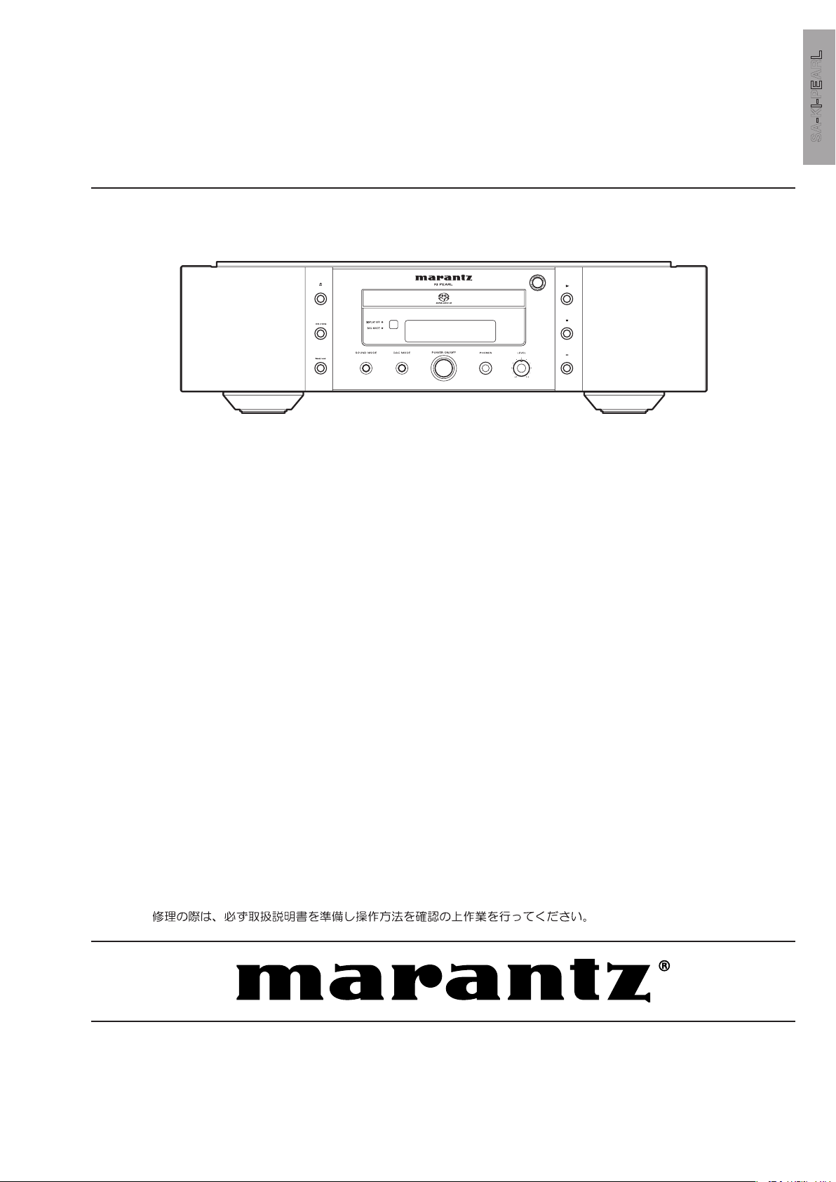
SA-KI-PEARL
NAMES AND FUNCTIONSBASIC CONNECTIONSBASIC OPERATION
ENGLISH
OPEN/
CLOSE
PLAY
STOP
PAUSE
SA-KI-PEARL /
N1B/U1B
Manual
SECTION PAGE
1. TECHNICAL SPECIFICATIONS ........................................................................................... 1
2. SERVICE HINTS AND TOOLS ............................................................................................. 4
3. WARNING AND LASER SAFETY INSTRUCTIONS ............................................................ 5
4. CAUTIONS ........................................................................................................................... 6
5. UPDATA FIRMWARE PROCEDURE .................................................................................... 8
6. SERVICE MODE ..................................................................................................................15
7. HOW TO THE RESET OF PLAYBACK TIME ......................................................................17
8. ERROR MESSAGE .............................................................................................................18
9. TROUBLESHOOTING ....................................................................................................... 25
10. WARNING DIAGRAM ..........................................................................................................27
11. BLOCK DIAGRAM .............................................................................................................. 29
12. SCHEMATIC DIAGRAM ......................................................................................................31
13. PARTS LOCATION ............................................................................................................. 43
14. EXPLODED VIEW AND PARTS LISTA .............................................................................. 53
15. MICROPROCESSOR AND IC DAT .....................................................................................57
16. ELECTRICAL PARTS LIST ................................................................................................ 64
17. ABOUT REPLACE THE MICROPROCESSOR WITH A NEW ONE ...............................75
Super Audio CD Player
TABLE OF CONTENTS
Please use this service manual with referring to the user guide ( D.F.U. ) without fail.
SA-KI-PEARL
Part no. 90M36AK855010
First Issue 2009.03
MZ
Page 2
MARANTZ DESIGN AND SERVICE
USA
MARANTZ AMERICA, INC
100 CORPORATE DRIVE
MAHWAH, NEW JERSEY 07430
USA
EUROPE / TRADING
D&M EUROPE B. V.
P. O. BOX 8744, BUILDING SILVERPOINT
BEEMDSTRAAT 11, 5653 MA EINDHOVEN
THE NETHERLANDS
PHONE : +31 - 40 - 2507844
FAX : +31 - 40 - 2507860
KOREA
D&M SALES AND MARKETING KOREA LTD.
CHUNG JIN B/D., #1001,
53-5, WONHYORO 3 GA, YONGSAN-GU,
SEOUL, 140-719, KOREA
PHONE : +82 - 2 - 323 - 2155
FAX : +82 - 2 - 323 - 2154
CANADA
D&M Canada Inc.
5-505 APPLE CREEK BLVD.
MARKHAM, ONTARIO L3R 5B1
CANADA
PHONE : 905 - 415 - 9292
FAX : 905 - 475 - 4159
JAPAN
D&M BUILDING, 2-1 NISSHIN-CHO,
KAWASAKI-KU, KAWASAKI-SHI,
KANAGAWA, 210-8569 JAPAN
D&M Holdings Inc.
CHINA
D&M SALES AND MARKETING SHANGHAI LTD.
ROOM.808 SHANGHAI AIRPORT CITY TERMINAL
NO.1600 NANJING (WEST) ROAD, SHANGHAI,
CHINA. 200040
TEL : 021 - 6248 - 5151
FAX : 021 - 6248 - 4434
Using superior design and selected high grade components,
Only original
MARANTZ
parts can insure that your
MARANTZ
MARANTZ
product will continue to perform to the specifications for which
company has created the ultimate in stereo sound.
it is famous.
Parts for your
MARANTZ
ORDERING PARTS :
equipment are generally available to our National Marantz Subsidiary or Agent.
Parts can be ordered either by mail or by Fax.. In both cases, the correct part number has to be specified.
The following information must be supplied to eliminate delays in processing your order :
1. Complete address
2. Complete part numbers and quantities required
3. Description of parts
4. Model number for which part is required
5. Way of shipment
6. Signature : any order form or Fax. must be signed, otherwise such part order will be considered as null and void.
NOTE ON SAFETY :
Symbol Fire or electrical shock hazard. Only original parts should be used to replaced any part marked with symbol .
Any other component substitution (other than original type), may increase risk of fire or electrical shock hazard.
安全上の注意:
がついている部品は、安全上重要な部品です。必ず指定されている部品番号のものを使用して下さい。
SHOCK, FIRE HAZARD SERVICE TEST :
CAUTION : After servicing this appliance and prior to returning to customer, measure the resistance between either primary AC
cord connector pins ( with unit NOT connected to AC mains and its Power switch ON ), and the face or Front Panel of product
and controls and chassis bottom.
Any resistance measurement less than 1 Megohms should cause unit to be repaired or corrected before AC power is applied,
and verified before it is return to the user/customer.
Ref. UL Standard No. 60065.
In case of difficulties, do not hesitate to contact the Technical
Department at above mentioned address.
080702MZ
Page 3
1. TECHNICAL SPECIFICATIONS
NAMES AND FUNCTIONSBASIC CONNECTIONSBASIC OPERATION
ADVANCED CONNECTIONS
APPLICATION OPERATIONTROUBLESHOOTINGOTHERSOTHERS
ENGLISH
12
(1/2)
419 (16-1/2)
400 (15-3/4)
7
2channels
2Hz ~ 20kHz
2Hz ~ 20kHz (-0.15dB)
100dB
110dB
0.0015%
Precision of quartz
2.4V RMS stereo
30mW/32ohms (Variable maximum)
0.5Vp-p (75Ω)
-19dBm
-17.5dBm ~ -23dBm
AlGaAs
780nm
16-bit linear PCM
44.1kHz
NAMES AND FUNCTIONSBASIC CONNECTIONSBASIC OPERATION
ADVANCED CONNECTIONS
APPLICATION OPERATIONTROUBLESHOOTINGOTHERSOTHERS
ENGLISH
440 (17-3/8)
18
109 (4-5/16)
127 (5)
12
(1/2)
419 (16-1/2)
400 (15-3/4)
7
(5/16)
2channels
2Hz ~ 20kHz
2Hz ~ 20kHz (-0.15dB)
100dB
110dB
0.0015%
Precision of quartz
2.4V RMS stereo
30mW/32ohms (Variable maximum)
0.5Vp-p (75Ω)
-19dBm
-17.5dBm ~ -23dBm
AlGaAs
780nm
16-bit linear PCM
44.1kHz
Super Audio CD CD
Audio Characteristics
Analog output
Channels 2 channels 2 channels
Frequency range 2 Hz — 100 kHz 2 Hz — 20 kHz
Frequency characteristics 2 Hz — 50 kHz (-3 dB) 2 Hz — 20 kHz (-0.15 dB)
Dynamic range
S/N Ratio (A-weighted)
THD (1 kHz) 0.0010 % 0.0015 %
Wow & Flutter Precision of quartz Precision of quartz
Analog output level
Unbalanced 2.4 V RMS stereo 2.4 V RMS stereo
Headphone output level
Digital output level
Cinch JACK — 0.5 Vp-p (75 Ω)
Optical connector — -19 dBm
Digital input level
Rectangular optical connector — -17.5 dBm — -23 dBm
Optical Readout System
Laser AlGaAs AlGaAs
Wave length 650 nm 780 nm
Signal format 1-bit DSD 16-bit linear PCM
Sampling frequency 2.8224 MHz 44.1 kHz
Power Supply
Input Voltage, Frequency [N] ...................................................................AC 230 V 50/60 Hz
[U] ........................................................................AC 120 V 60 Hz
Power Consumption ...................................................................................................... 20 W
Cabinet, etc.
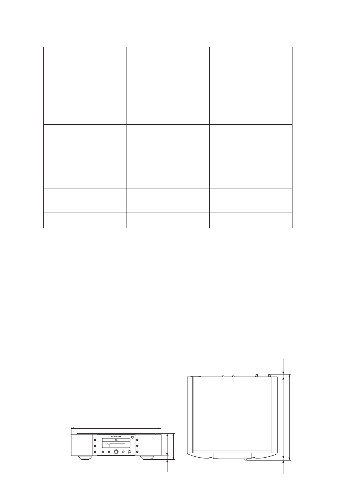
Dimensions (Width × Height × Depth) ............440 × 127 × 419 mm (17-3/8 × 5 × 16-1/2 in)
Net weight ................................................................................................... 14.5 kg (32.0 lb)
Operating temperatures ................................................................................ +5 °C ~ +35 °C
Operating humidity ............................................................................5 ~ 90 % (without dew)
Accessories
• Remote control unit (RC003SA) ........................................................................................1
Net weight .................................................................................................... 160 g (0.4 lb)
• AAA (R03) Batteries ..........................................................................................................2
• AC Power cord ...................................................................................................................1
• Audio cable ........................................................................................................................1
• Remote control connecting cord ........................................................................................1
• User’s Guide ......................................................................................................................1
DIMENSIONS
UNIT : in (mm)
112 dB
110 dB
30 mW (32 Ω, Variable maximum) 30 mW (32 Ω, Variable maximum)
100 dB
110 dB
1
Page 4
2
ENGLISH
FEATURES
APPLICABLE DISCS TO THE UNIT
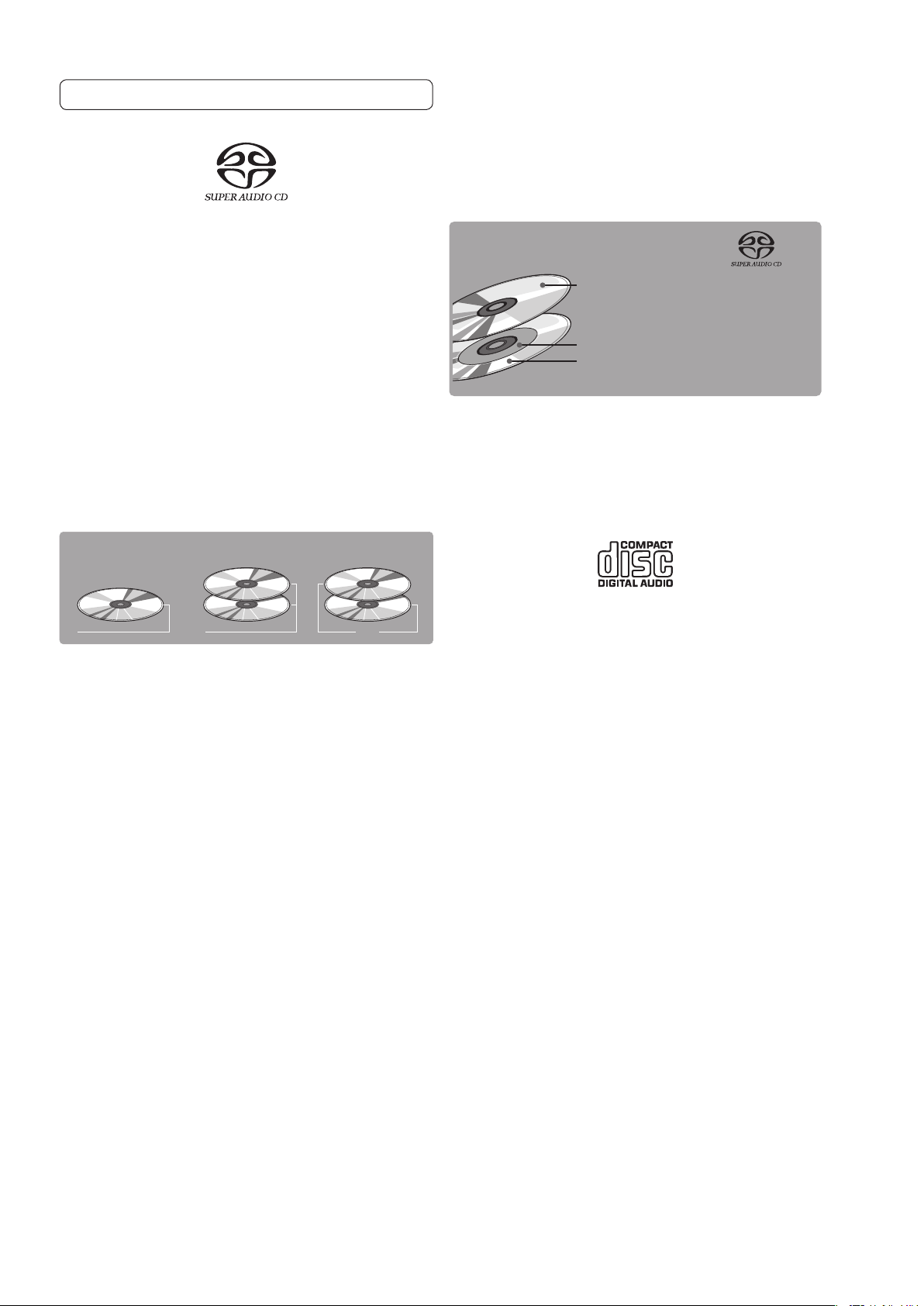
1. Super Audio CD
The Super Audio standard is based on Direct Stream Digital
(DSD) technology. This new direct-stream digital format
comprises a 1-bit system that has a digital sampling frequency
that is 64 times higher than that of conventional audio CD. The
results are spectacular: a frequency response of over 100kHz
and a 120 dB dynamic range over the entire audible spectrum.
Mixed with as many of the original frequencies as possible,
the audio information audible for human ears sounds much
more natural.
All audible frequencies are, after all, embedded in the frequency
range as emitted by the sound source. A better reproduction
does not exist! For the first time your ears will relive reality.
There are three types of Super Audio CDs.
• Single-layer Disc
• Dual-layer Disc
• Hybrid-layer Disc
Disc Types
Single-layer Disc
Dual-layer Disc
Hybrid-layer Disc
HD layer HD layer CD layer HD layer
And each type may contain two areas of recorded information.
• High quality stereo area
• High quality multi-channel area**
• Single Layer Disc
It can contain both high quality stereo area and high quality
multi-channel area** information.
• Dual Layer Disc
It can contain both high quality stereo area and high quality multichannel area** information. And a double amount of information
can be stored on the disc thanks to the second layer.
• Hybrid Layer Disc
Not only does this disc contain both high sound quality stereo
area and high sound quality multi-channel area** information,
it also has a CD layer in the second layer, so it can be played
on a CD player.
Hybrid Super Audio CD Disc
1 CD layer that plays on any of your
existing CD players
High-Density layer containing:
2 - High sound quality stereo
3 -
High sound quality multi-channel**
The number of tracks recorded may vary per layer.
**This unit is a stereo-only player, and so it cannot play
high-quality multi-channel audio areas. (It does not
recognize multi-channel areas.)
2. Audio CD (CDDA)
Audio CDs contain music tracks only.
3. CD-R / CD-RW
This unit can play back the CD-RW (ReWritable) discs as well
as ordinary Audio CD and CD-R (Recordable) discs.
•
The CD-R and CD-RW discs should contain properly-recorded
TOC* information so that they can be played back. In CD
recorders, the task of writing TOC information is referred to as
finalizing the disc. Discs that are not finalized cannot be properly
recognized as an Audio CD and played back by regular CD
players and Super Audio CD players. For details, please read
the instruction manual provided with a CD recorder.
* TOC stands for Table Of Contents and contains information
such as the total number of tracks and total playing time
of the disc.
•
As the playback of a CD-RW disc necessitates partial change
of the player setup, it may take longer time for reading the TOC
information than when an Audio CD or CD-R disc is played.
Page 5
3
本機で再生できるディスクについて
1.スーパーオーディオCD
スーパーオーディオ CD 規格はダイレクト・ストリーム・デ
ジタル(DirectStreamDigital)(DSD)技術に基づいています。
このダイレクト・ストリーム・ デジタル・フォーマットは、
従来のオーディオ C D よりも 64 倍のサンプリング周波数を
有する 1 ビットシステムから構成されています。
それによって、100kHz 以上におよぶ周波数範囲及び可聴周
波数帯全域でダイナミックレンジ 120dB の素晴らしいサウ
ンドが生まれます。
可能な限り多くの周波数分布をミックスすることにより、可
聴域のオーディオ情報がよりいっそう自然に聞こえるように
なります。
つまり、すべての可聴周波数は音源から発せられる周波数範
囲内に組み込まれます。
これによって、リアリティーのある音場が再現されます。
スーパーオーディオ CD には、以下の 3 つのタイプがあります。
•シングルレイヤー・ディスク
•デュアルレイヤー・ディスク
•ハイブリッドレイヤー・ディスク
ディスクタイプ
シングルレイヤー
ディスク
デュアルレイヤー
ディスク
ハイブリッドレイヤー
ディスク
HDレイヤー HDレイヤー HDレイヤー
CDレイヤー
また、各々のタイプは、情報が記録される 2 つの領域、
•高音質ステレオエリア
•高音質マルチチャンネルエリア**
を持つことができます。
•シングルレイヤー・ディスク
高音質ステレオと高音質マルチチャンネル ** の両方の情報
エリアを持つことができます。
•デュアルレイヤー・ディスク
高音質ステレオと高音質マルチチャンネル ** の両方の情
報エリアを持つことができますが、第二レイヤーの存在に
よって 2 倍の情報量をディスクに記憶することができます。
•ハイブリッドレイヤー・ディスク
高音質ステレオと高音質マルチチャンネル ** の両方の情報
エリアを持てるだけでなく、第二レイヤーには CD レイヤー
も持てるため、CD プレーヤーでの再生が可能となります。
1 既存のCDプレーヤーで
再生可能なCDレイヤー
HybridSuperAudioCDディスク
高密度レイヤーは次の内容で構成されます。
2 - 高音質ステレオ
3 - 高音質マルチチャンネル
**
記録されるトラック数は、レイヤーによって違うことがあり
ます。
** 本機はステレオ専用プレーヤーですので高音質マルチ
チャンネルエリアは再生できません。(マルチチャンネ
ルエリアは認識しません)
2.オーディオ(音楽)CD(CDDA)
本機の特長
また、各々のタイプは、情報が記録される 2 つの領域、
•高音質ステレオエリア
•高音質マルチチャンネルエリア**
を持つことができます。
•シングルレイヤー・ディスク
高音質ステレオと高音質マルチチャンネル ** の両方の情報
エリアを持つことができます。
•デュアルレイヤー・ディスク
高音質ステレオと高音質マルチチャンネル ** の両方の情
報エリアを持つことができますが、第二レイヤーの存在に
よって 2 倍の情報量をディスクに記憶することができます。
•ハイブリッドレイヤー・ディスク
高音質ステレオと高音質マルチチャンネル ** の両方の情報
エリアを持てるだけでなく、第二レイヤーには CD レイヤー
も持てるため、CD プレーヤーでの再生が可能となります。
1 既存のCDプレーヤーで
再生可能なCDレイヤー
HybridSuperAudioCDディスク
高密度レイヤーは次の内容で構成されます。
2 - 高音質ステレオ
3 - 高音質マルチチャンネル
**
記録されるトラック数は、レイヤーによって違うことがあり
ます。
** 本機はステレオ専用プレーヤーですので高音質マルチ
チャンネルエリアは再生できません。(マルチチャンネ
ルエリアは認識しません)
2.オーディオ(音楽)CD(CDDA)
オーディオ CD はミュージックトラックのみで構成されてい
ます。
3.CD-R/CD-RW
•CD-R や CD-RW の再生では必ず TOC* が正しく記録され
ていることが必要です。CD レコーダーでは TOC 情報を書
き込むことをファイナライズ(Finalize)といい、この作業が
正常に完了していないディスクは、普通の C D プレーヤー
やスーパーオーディオ CD プレーヤーではオーディオ C D
として正しく認識されず再生することができませんので十
分ご注意ください。詳しくは CD レコーダーの取扱説明書
をご覧ください。
*TOC(トック)とは Table Of Contents の略で、ディスク
の総曲数や総再生時間などの目次情報のことです。
•CD-RW ディスクを再生する場合、プレーヤーの設定を一
部変更するため、オーディオ CD や C D - R に比べ TOC の
読み込みに若干時間がかかることがあります。
Page 6
4
2. SERVICE HINTS AND TOOLS
DVD test disc (NTSC) ALMEDIO TDV-540
SERVICE TOOLS
Audio signals disc 4822 397 30184 or TCD-784
Disc without errors +
Disc with DO errors, black spots and fingerprints 4822 397 30245 (SBC444A) or TCD-726
Disc (65 min 1kHz) without no pause 4822 397 30155
Max. diameter disc (58.0 mm) 4822 397 60141
Torx screwdrivers
Set (straight) 4822 395 50145
Set (square) 4822 395 50132
13th order filter 4822 395 30204
DVD test disc (PAL) 4822 397 10131
SERVICE HIN
TS
070703MZ
Page 7
5
3. WARNING AND LASER SAFETY INSTRUCTIONS
F
ATTENTION
Tous les IC et beaucoup d’autres semiconducteurs sont sensibles aux décharges
statiques (ESD).
Leur longévité pourrait être considérablement
écourtée par le fait qu’aucune précaution
n’est prise a leur manipulation.
Lors de réparations, s’assurer de bien être
relié au même potentiel que la masse de
l’appareil et enfiler le bracelet serti d’une
résistance de sécurité.
Veiller a ce que les composa
nts ainsi que les
outils que l’on utilise soient également a ce
potentiel.
D
WARNUNG
Alle IC und viele andere Halbleiter sind
empfindlich gegen elektrostatische
Entladungen (ESD).
Unsorgfältige Behandlung bei der Reparatur
kann die Lebensdauer drastisch vermindern.
Sorgen sie dafür, das Sie im Reparaturfall
über ein Pulsarmband mit Widerstand mit
dem Massepotential des Gerätes verbunden
sind.
Halten Sie Bauteile und Hilfsmittel ebenfalls
auf diesem Potential.
WAARSCHUWING
Alle IC’s en vele andere halfgeleiders zijn
gevoelig voor elektrostatische ontladingen
(ESD).
Onzorgvuldig behandelen tijdens reparatie
kan de levensduur drastisch doen
verminderen.
Zorg ervoor dat u tijdens reparatie via een
polsband met weerstand verbonden bent met
hetzelfde potentiaal als de massa van het
apparaat.
Houd componenten en hulpmiddelen ook op
ditzelfde potentiaal.
AVVERTIMENTO
Tutti IC e parecchi semi-conduttori sono
sensibili alle scariche statiche (ESD).
La loro longevita potrebbe essere fortemente
ridatta in caso di non osservazione della piu
grande cauzione alla loro manipolazione.
Durante le riparazioni occorre quindi essere
collegato allo stesso potenziale che quello
della massa dell’apparecchio tramite un
braccialetto a resistenza.
Assicurarsi che i componenti e anche gli
utensili con quali si lavora s
iano anche a
questo potenziale.
All ICs and many other semi-conductors are
susceptible to electrostatic discharges (ESD).
Careless handling during repair can reduce
life drastically.
When repairing, make sure that you are
connected with the same potential as the
mass of the set via a wrist wrap with
resistance.
Keep components and tools also at this
potential.
WARNING
Safety regulations require that the set be restored to its original condition
and that parts which are identical with those specified be used.
Veiligheidsbepalingen vereisen, dat het apparaat in zijn oorspronkelijke
toestand wordt terug gebracht en dat onderdelen, identiek aan de
gespecifieerde worden toegepast.
Bei jeder Reparatur sind die geltenden Sicherheitsvorschriften zu beachten.
Der Originalzustand des Gerats darf nicht verandert werden
.
Fur Reparaturen sind Original-Ersatzteile zu verwenden.
Le norme di sicurezza esigono che l’apparecchio venga rimesso nelle
condizioni originali e che siano utilizzati pezzi di ricambiago idetici a quelli
specificati.
Les normes de sécurité exigent que l’appareil soit remis a l’état d’origine et
que soient utilisées les pièces de rechange identiques à celles spécifiées.
“Pour votre sécurité, ces documents
doivent être utilisés par des
spécialistes agrées, seu ls habilités à
réparer votre appareil en panne.”
GB
NL
I
D
I
F
GB
NL
LASER SAFETY
CAUTION VISIBLE AND INVISIBLE LASER RADIATION WHEN OPEN AVOID EXPOSURE TO BEAM
ADVARSEL SYNLIG OG USYNLIG LASERSTRÅLING VED ÅBNING UNDGÅ UDS
Æ
TTELSE FOR STRÅLING
ADVARSEL SYNLIG OG USYNLIG LASERSTRÅLING NÅR DEKSEL Å PNES UNNGÅ EKSPONERING FOR STRÅLEN
VARNING SYNLIG OCH OSYNLIG LASERSTRÅLNING NÄR DENNA DEL ÄR ÖPPNAD BETRAKTA EJ STRÅLEN
VARO! AVATT AESSA OLET ALTTIINA NÄKYVÄLLE JA NÄKYMÄTTÖMÄLLE LASER SÄ
TEILYLLE. ÄLÄ KATSO SÄTEESEEN
VORSICHT SICHTBARE UND UNSICHTBARE LASERSTRAHLUNG WENN ABDECKUNG GEÖFFNET NICHT DEM STRAHL AUSSETSEN
DANGER VISIBLE AND INVISIBLE LASER RADIATION WHEN OPEN AVOID DIRECT EXPOSURE TO BEAM
ATTENTION RAYONNEMENT LASER VISIBLE ET INVISIBLE EN CAS D'OUVERTURE EXPOSITION DANGEREUSE AU FAISCEAU
USE OF CONTROLS OR ADJUSTMENTS OR PERFORMANCE OF PROCEDURE OTHER THAN THOSE
SPECIFIED H
EREIN MAY RESULT IN HAZARDOUS RADIATION EXPOSURE.
AVOID DIRECT EXPOSURE TO BEAM
WARNING
The use of optical instruments with this product will increase eye hazard.
Repair handling should take place as much as possible with a disc loaded inside the player
WARNING LOCATION: INSIDE ON LASER COVERSHIELD
This unit employs a laser. Only a qualified service person should remove the cover or attempt to service t
his
device, due to possible eye injury.
030804ecm
Page 8
6
4. CAUTIONS
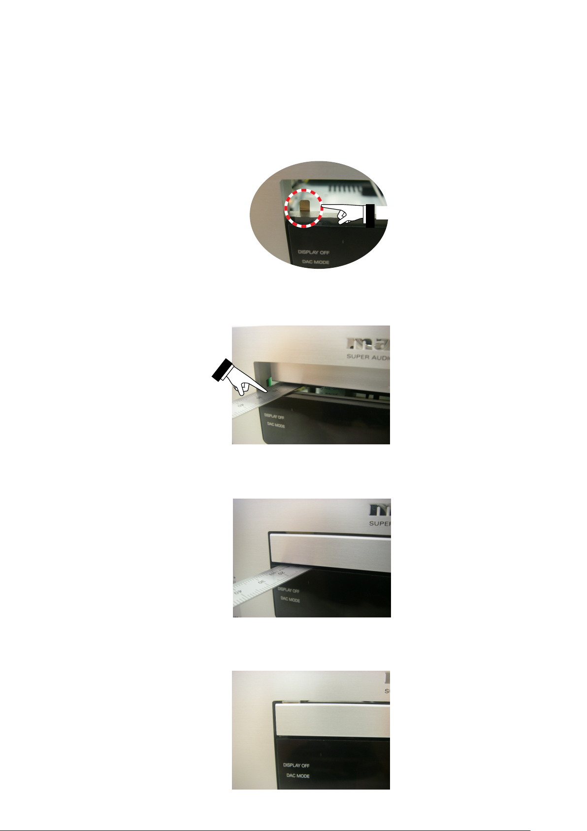
[A] TAKING THE DISC OUT OF EMERGENCY
Remove the top cover of the player.1.
Remove the cover of Loader.2.
Remove 2 screws shown in the picture follows.3.
Remove the disc clamper.4.
Now you can remove the disc.5.
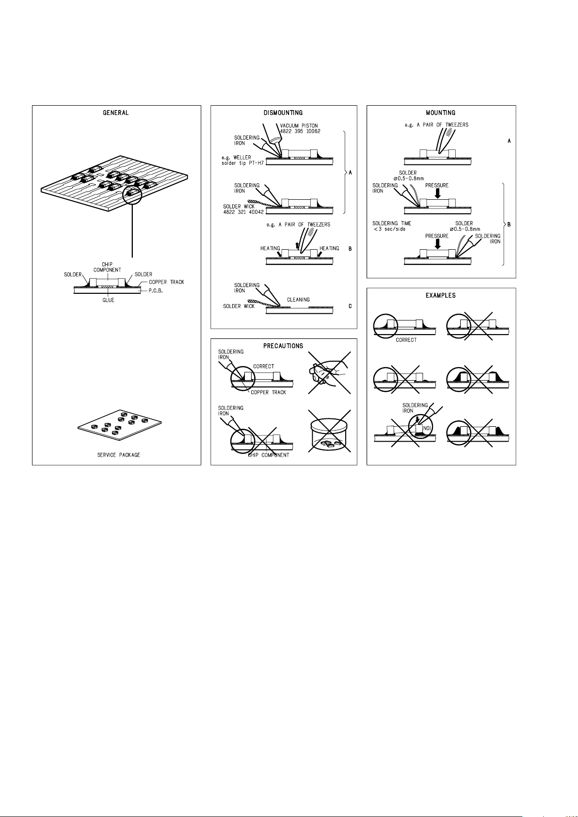
[B] CAUTIONS IN ASSEMBLING AND
DISASSEMBLING (M002)
When removing the FFC (flexible flat cable), connecting
the optical pick up and the Super Audio CD PWB, short
the short three lands pointed by the arrow with solder.
Otherwise the laser diode may be damaged by static
electricity.
[B] 取り外し、組み立て時の注意 (M002)
ピックアップ(レーザーダイオード)の静電破壊による損傷を
避けるため下記の作業を行ってください。
FFCケーブルを外す前に、ピックアップ基板の3つのショー1.
トランド(矢印)を半田でショートします。
FFCケーブルを接続後、ショートランドの半田を取り除き2.
ます。
FFC
Short the three short lands by soldering
3つのショートランド(矢印)を半田でショートします
Page 9
7
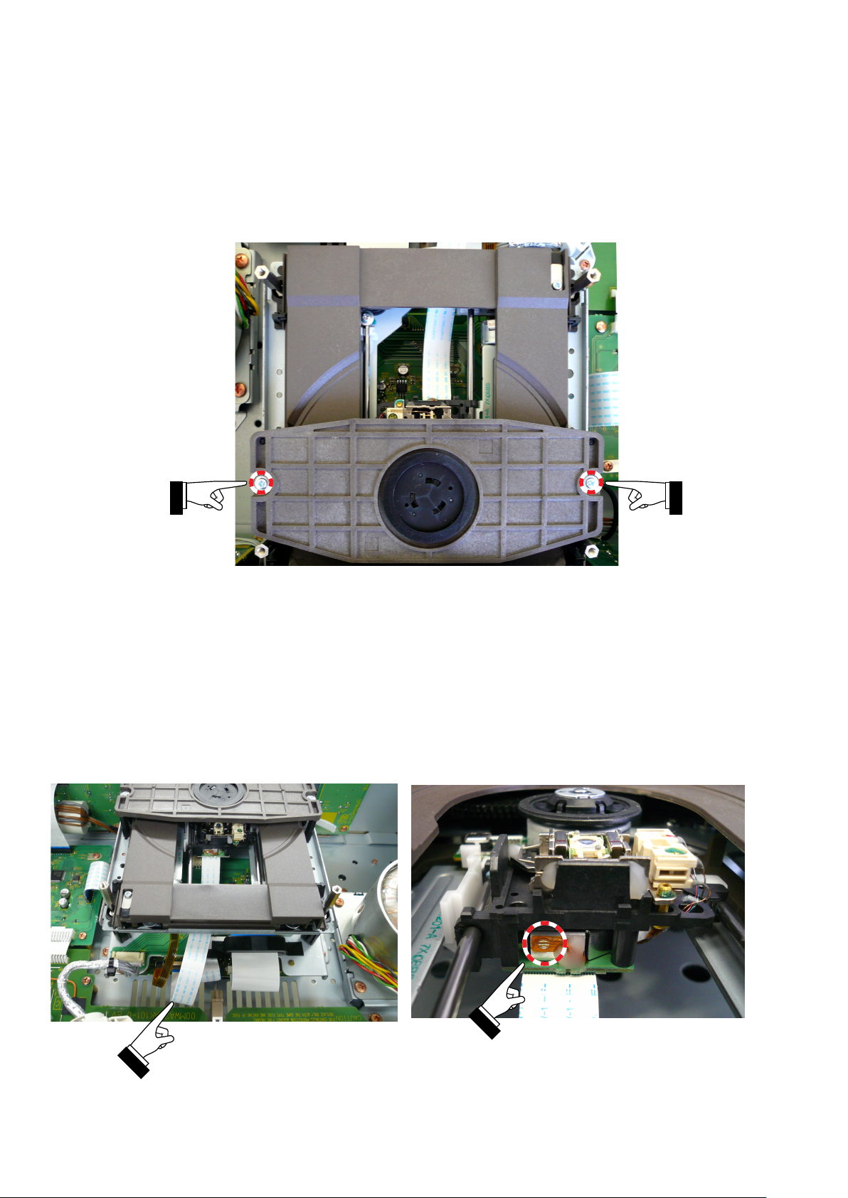
[C] PRECAUTIONS TO OBSERVE IN INSTALLING
THE LOADER UNIT
Due to the contactor (021B) being deformable, when
installing the loader unit at the time of repair, please follow
the procedure mentioned below.
[C] LOADER UNIT取り付け時の注意事項
修理時LOADER UNITを後から取り付ける際は、コンタクター
(021B)が変形しやすいため、下記の手順でLOADER UNITを取
り付けてください。
The contactor (021B) is a thin copper plate.
Hold down the 021B with a thin plate while installing the 1.
loader unit.
薄い板等で押さえる
Hold it down with a thin
plate.
コンタクター(021B) : 薄い銅版です。
021B
(021B)を薄い板等で押さえながら、LOADER UNITを取り1.
付けてください。
Keep holding it down with a thin plate until the loader unit 2.
gets in position.
When the loader unit is installed, pull out the thin plate 3.
that has held down the 021B.
LOADER UNITが定位置に取り付くまで薄い板等で押さえ2.
ます。
LOADER UNITを取り付け後、差し込んでいた薄い板を抜3.
きます。
Page 10
8
5. UPDATE FIRMWARE PROCEDURE
[A] Update Front CPU's software to internal Flash-
ROM.
• This mode is to update the software for Front CPU’s.
• The target devise is internal flash ROM of Front CPU’s
(QF01) on MPU/DIR PWB (PU16).
• The updating of software takes about 1 minute.
5. UPDATE FIRMWARE PROCEDURE
[A] Update Front CPU's software to internal Flash-
ROM.
• このモードはフロントマイコンの更新用です。
• MPU/DIR PWB (PU16) のQF01のマイコン内部のフラッシ
ュROMに書き込みます。
• 書き込みにかかる時間は約1分です。
Necessary Equipment
The following items are required for updating.
• Windows PC (OS: Windows2000 or WindowsXP) with
Serial port.
• RS-232C Dsub-9 pin cable (female to female/straight
type)
• Update software to CPU. (FlashSta.exe, SACD_
yymmddvv.mot and SACD_yymmddvv.id in Front CPU
(KI-13S2) folder)
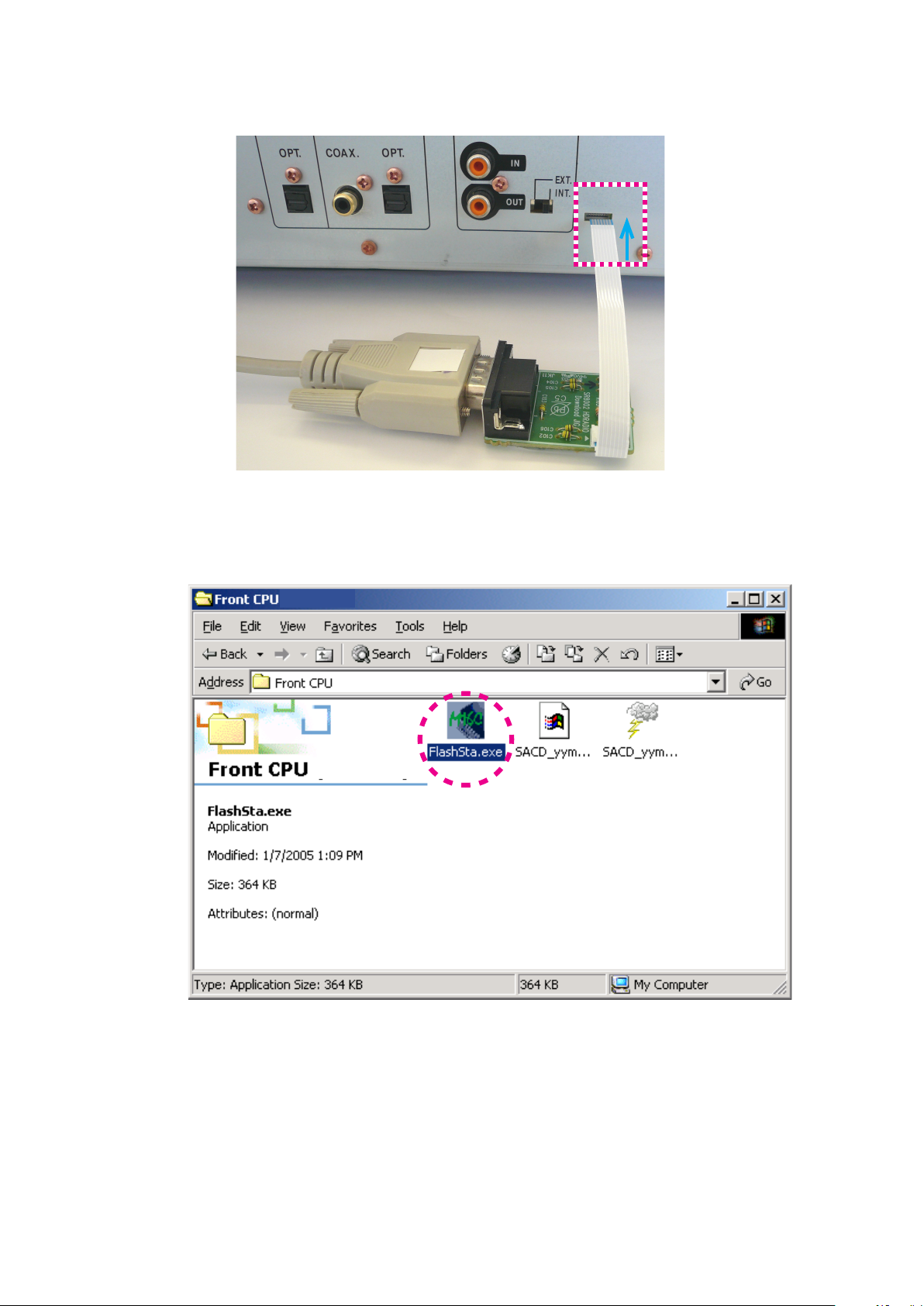
• DATA UPDATE KIT (part no. 90M-SR4001JIG)
Use DATA UPDATE KIT to connect PC and JU01 (FFC
connector) in rear panel of the unit, when updating Front
CPU
Update Software for Front CPU
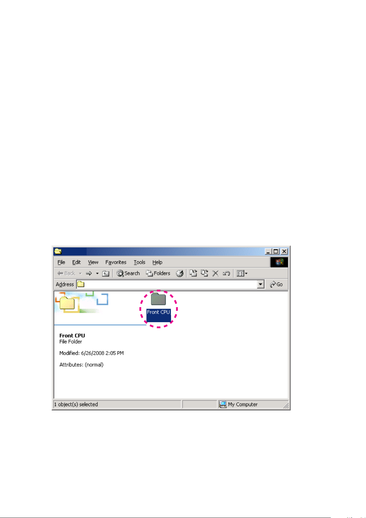
Put the "Front CPU (KI-13S2)" folder into anywhere on 1.
your PC's hard disc.
KI-13S2
必要機器
下記は更新に必要な機器です。
• Windows PC (OS : Windows2000 またはWindowsXP) で
Serial ポートのあるもの
• RS-232C ストレートケーブル(9Pin メス-9Pin メス)
• マイコン用書き込みソフトウェア(Front CPU (KI-13S2)
フォルダ内FlashSta.exeおよびSACD_yymmddvv.mot,
SACD_yymmddvv.id)
• DATA UPDATE KIT (part no. 90M-SR4001JIG)
マイコンのファームウェアを更新する場合、DATA UPDATE
KITを使用しPCと本機のリアパネル内にあるJU01とを接続し
ます。
Update Software for Front CPU
1. Front CPU (KI-13S2)フォルダをPCの任意のフォルダに1.
コピーします。
Connect PC and DATA UPDATE KIT with the RS-232C 2.
cable.
KI-13S2
KI-13S2
(KI-13S2)
(KI-13S2)
DATA UPDATE KITとPCとをRS-232Cケーブルで接続し2.
ます。
Page 11
9
Connect FPC (upside contact) to the rear panel of the 3.
unit from DATA UPDATE KIT
DATA UPDATE KITのFFCを接点を上にして、本機のリア3.
パネルに接続します。
Connect the mains cord into the unit.4.
Double click the FlashSta.exe. And launch the M16 Flash 5.
Start.
本機に電源ケーブルを接続します。4.
FlashSta.exeをダブルクリックし、Flash Startを起動しま5.
す。
(KI-13S2)
(KI-13S2)
(KI-13S2)
Page 12
10
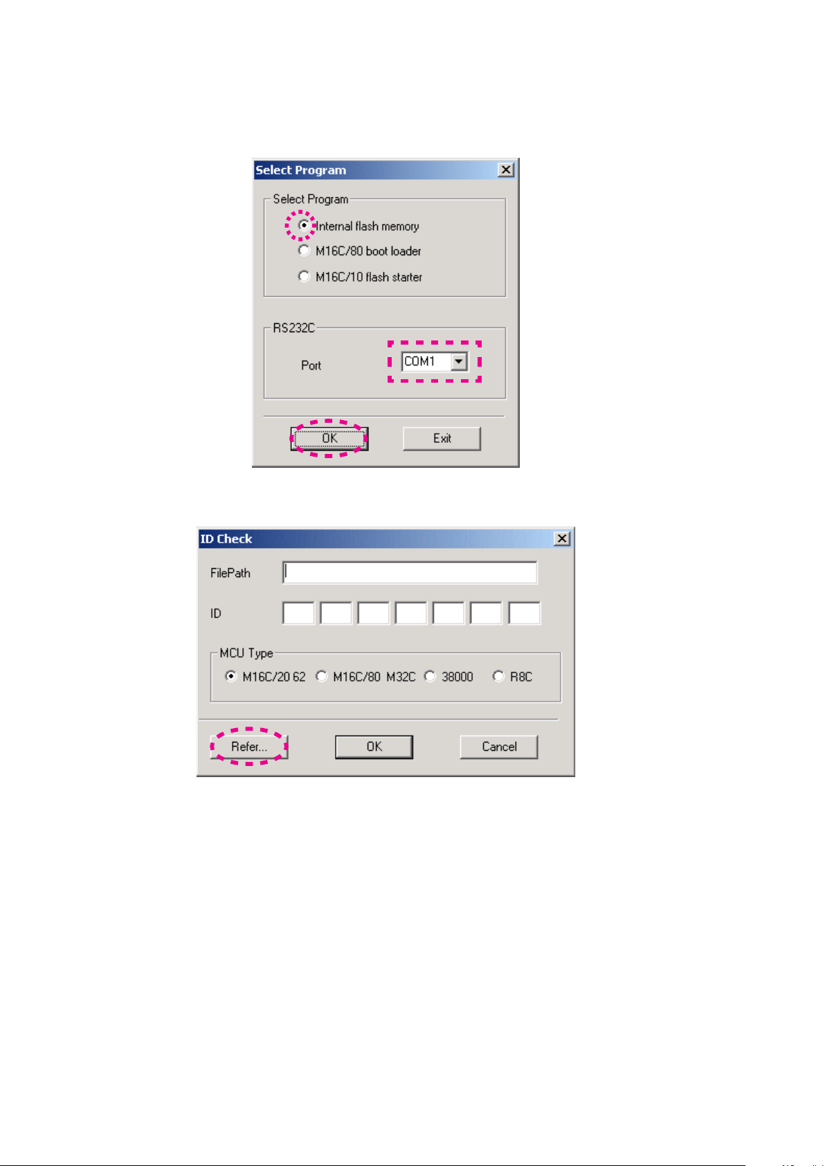
Check the 6. Internal flash memory in the Select Program.
Choose the COM Port number.
And click the OK.
Select Programの6. Internal flash memoryにチェックをし
て下さい。
使用するCOMポート番号を選択します。
OKをクリックします。
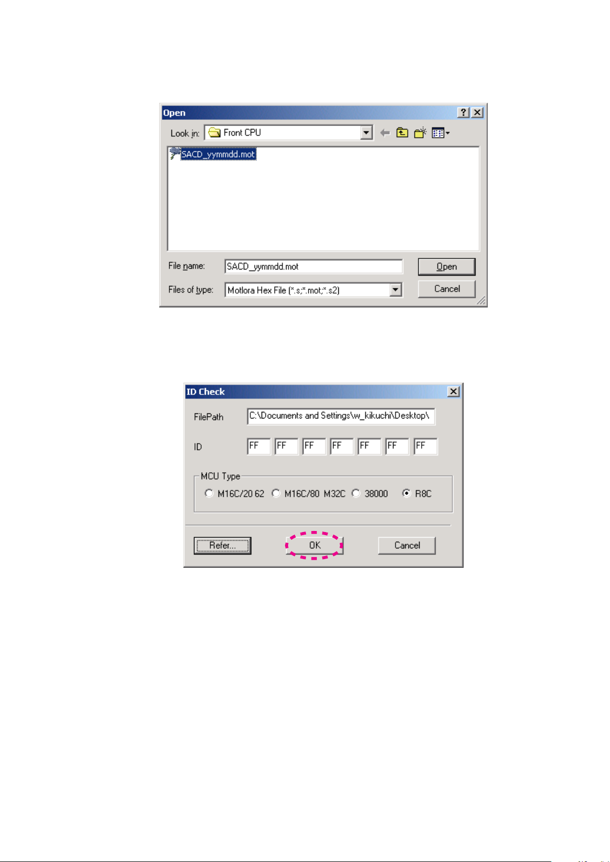
Click the 7. Refer....
Refer...7. をクリックします。
Page 13
11
Choose the SACD_yymmdd.mot. And click the 8. Open.
NOTE : The yy is two digits of year. The mm is month. The
dd is date.
(KI-13S2)
SACD_yymmdd.motを選択し、8. Openをクリックします。
注意 : yyは年の下二桁、mmは月、ddは日
The FilePath and ID are inputted automatically, and the 9.
MCU Type is selected to R8C automatically.
Click the OK.
FilePathとIDは自動的に記入され、MCU TypeはR8Cが選9.
ばれます。
OKをクリックします。
Page 14

12
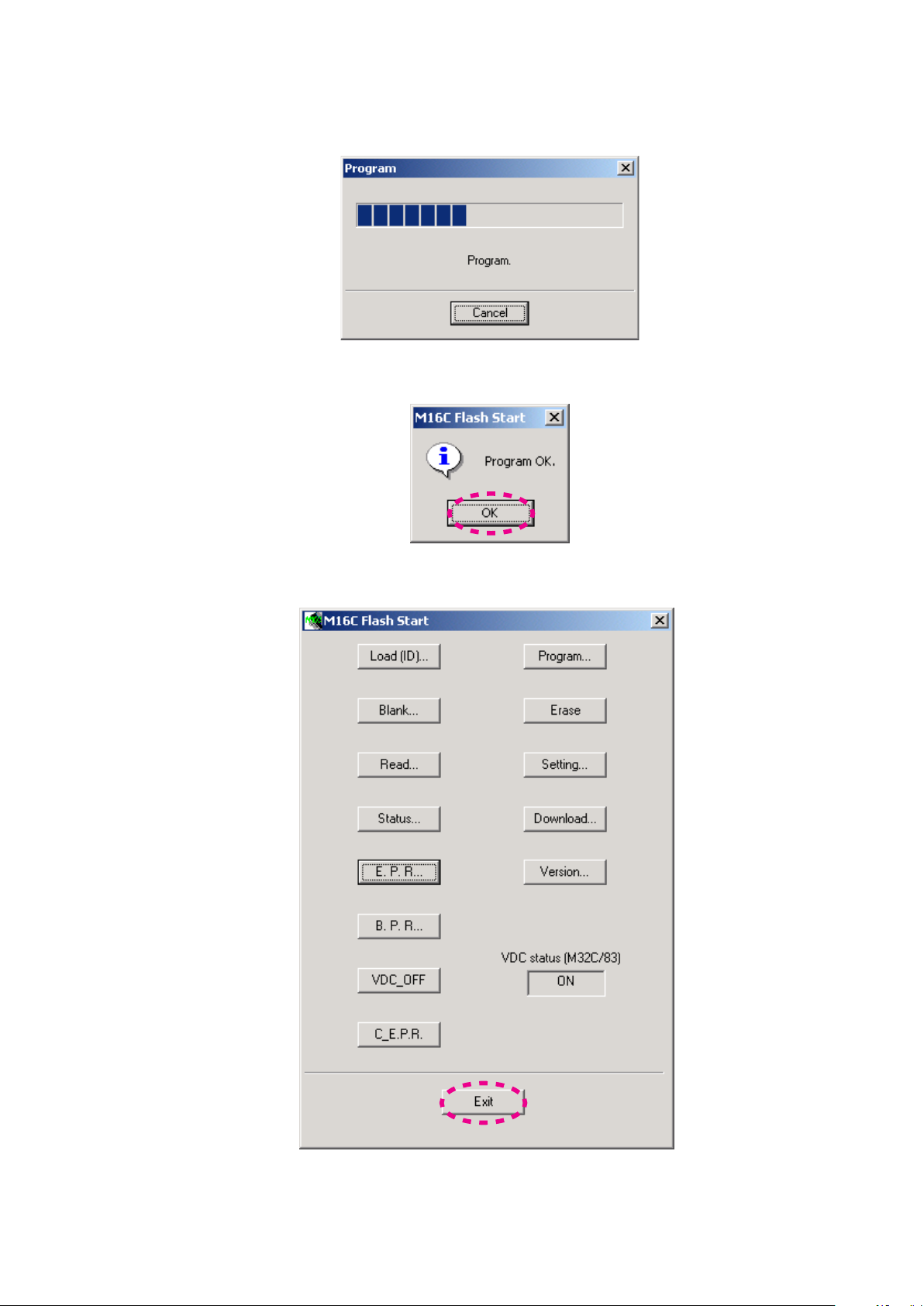
Click the 10. E.P.R....
E.P.R...10. をクリックします。
Click the 11. OK.
OK11. をクリックします。
Page 15
13
Software is written into the internal Flash-ROM of Front 12.
CPU.
The writing of software takes about 1 minute.
Click the 13. OK.
ソフトウェアがFront CPUの内部フラッシュROMに書き込12.
まれます。
書き込みにかかる時間は約1分です。
OK13. をクリックします。
Click the 14. Exit.
Exit14. をクリックします。
Disconnect the mains cord.15.
Disconnect the FFC of DATA UPDATE KIT from the unit.16.
本機から電源コードを外します。15.
本機からDATA UPDATE KITのFFCを抜きます。16.
Page 16

14
[B] UPDATE FIRMWARE FOR Super Audio CD
MODULE
[B] UPDATE FIRMWARE FOR Super Audio CD
MODULE
NECESSARY EQUIPMENT
• Update Disc (90M-KI13S2CDR)
WRITING PROCEDURE
Connect the mains cord into the unit.1.
Turn on the unit.2.
Press the 3. OPEN/CLOSE button to open the tray.
Insert the Update Disc.4.
Press the 5. OPEN/CLOSE button to close the tray.
"Upgrade?" is displayed on the front display. Then Press 6.
PLAY button.
Remove the update disc from the tray, when the tray is 7.
opened automatically. At that time ""Upgrade" is blinking
on the front display.
When update succeeded, the tray is closed automatically.8.
And "No Disc" is displayed on the front display.9.
Turn off the unit.10.
Disconnect the mains cord from the unit.11.
NECESSARY EQUIPMENT
• Update Disc (90M-KI13S2CDR)
WRITING PROCEDURE
本機に電源コードを接続します。1.
本機の電源を入れます。2.
OPEN/CLOSE3. ボタンを押しトレイを開きます。
Update Discをトレイに乗せます。4.
OPEN/CLOSE5. ボタンを押しトレイを閉じます。
フロントディスプレイに6. "Upgrade?"が表示された
ら、PLAYボタンを押します。
トレイが自動的に開いたらUpdate Discをトレイから取り出7.
します。このときフロントディスプレイに"Upgrade"と表示
され点滅します。
アップデートが完了すると自動的にトレイが閉じます。8.
フロントディスプレイに9. "No Disc"と表示されます。
本機の電源を切ります。10.
本機から電源コードを外します。11.
Page 17
15
6. SERVICE MODE
RPT
RNDM
PROG TRK CD M FILE USB STRG D OFF REMAIN TTLA- B 1
INVDCFN SHP
ALL
FIL 1 2 3 AMS STEREO EXT CLK 44.1K 88.2K 176.4K
INVDCFN SHP
INVDCFN SHP
6. SERVICE MODE
Insert mains cable plug in the outlet.1.
Press the 2. POWER ON/OFF button While pressing
g/i and STOP button.
Model name is displayed.
SA13 /K I
Press 3. g/i button Press j/h button
Version of FRONT microprocessor is displayed.
FR2008090902
Press 4. g/i button Press j/h button
Number of SUPER AUDIO CD module ROM is displayed.
SROM : AYW7260
Press 5. g/i button Press j/h button
Version of SUPER AUDIO CD module ROM is displayed.
SVer :_1.21
電源コードを接続します。1.
2. g/iボタンとSTOPボタンを押しながらPOWER ON/
OFFボタンを押します。(以下、表示例は英文項の図を参
照)
DISPLAYに機種名が表示されます。
3. g/iボタンを押します。戻るには j/hボタンを
押します。
DISPLAYにFRNOT Micro-Processor Versionが表示されま
す。
4. g/iボタンを押します。戻るには j/hボタンを
押します。
DISPLAYにSUPER AUDIO CDモジュールのROM 番号が
表示されます。
5. g/iボタンを押します。戻るには j/hボタンを
押します。
DISPLAYにSUPER AUDIO CDモジュールのROM Version
が表示されます。
Press 6. g/i button Press j/h button
6. g/iボタンを押します。戻るには j/hボタンを
押します。
All area in the LCD light on.
Press 7. g/i button Press j/h button
LCDが全点灯します。
7. g/iボタンを押します。戻るには j/hボタンを
押します。
Turn off all LCD segments.
Press 8. g/i button Press j/h button
LCDが全消灯します。
8. g/iボタンを押します。戻るには j/hボタンを
押します。
Serial number is displayed.
DISPLAYにSERIAL NOが表示されます。
20_000000000
Press 9. g/i button Press j/h button
[A] DISPLAYにDISC 再生時間(総合計)が表示されます。
[A] SUPER AUDIO CD payback time is displayed. [B] SUPER AUDIO CD backup time is displayed.
Press PLAY button
PTime : 00021h BTime : 00021h
Press PAUSE button
Press 10. g/i button Press j/h button
9. g/iボタンを押します。戻るには j/hボタンを
押します。
[B] SUPER AUDIO CDのバックアップされた時間が表示されます。
10. g/iボタンを押します。戻るには j/hボタンを
押します。
Page 18

16
[A] DISPLAYにCD再生時間(総合計)が表示されます。
INVDCFN SHP
INVDCFN SHP
[B] CDのバックアップされた時間が表示されます。
[A] CD playback time is displayed. [B] CD backup time is displayed.
Press PLAY button
PTime : 00021h
BTime : 00021h
Press PAUSE button
Backup time (BTime) :
When replacing SUPER AUDIO CD module and reset
playback times
(total), the software is available that automatically backs
up (saves) playback times (total). You can check the
information before replacing SUPER AUDIO CD module.
Press the POWER ON/OFF button to quit Service Mode.
Factory Mode
To reset the back up memory of the unit into the default
status, follow the procedure below.
Connect the mains cord into the unit and press 1. STOP
and POWER ON/OFF button simultaneously more than
3 seconds.
"Reset2. " is displayed, after "Reset OK" displayed on the
display, and EEPROM is cleared to the default status,
microprocessor is reset and unit returns to the normal
status.
バックアップ時間 (BTime):
SUPER AUDIO CDモジュールを交換した際、再生時間(
総合計)のクリア作業を行いますが、その時に交換する前
のSUPER AUDIO CDモジュールの再生時間(総合計)が
メモリにバックアップされます。その情報を確認すること
が出来ます。
電源を切るとSERVCICE モードが解除されます。
初期状態にするには(リセット)
電源コードを接続します。1. STOPとPOWER ON/OFFボタ
ンを同時に約3秒以上押します。
ディスプレイに2. "Reset"が表示され、その後"Reset OK"が
表示され通常状態の表示に戻り、初期化が終了します。
Page 19

17
7. HOW TO THE RESET OF PLAYBACK TIME
7. DISC再生時間のリセット(初期化)方法
When replacing CD MECHANISM [ 001M or M002 ]
(TRAVERSE Block), please reset Playback time (total) in the
following procedure.
Procedure 11, 12 of SERVICE MODE, Playback time 1.
(total) is displayed.
PTime : 10051h
The display is a time unit. (Example: "10050 hours, 0
minute, 1 second" is 10051h)
The maximum Playback time is 65536h.
Press 2. C (STOP) Button 3 seconds and more.
PTime Clear? is displayed.
PTime Clear?
Press 3. B (PLAY) Button.
Done is displayed after PTime:00000h is displayed.
Play back time (total) was reset.
新しいCD MECHANISM [ 001M or M002 ] (TRAVERSE部)
に交換した場合、次の手順でDISC再生時間をリセット(初期
化)してください。
SERVICE MODE の手順11, 12でDISPLAYにDISC 再生時1.
間(合計)が表示されます。
表示は時間単位です。(例:10050時間0分1秒は10051h
となります)
最大表示は、65536hまでです。
2. C (STOP)ボタンを3秒以上押します。
DISPLAYにPTime Clear?と表示されます。
3. B (PLAY)ボタンを押します。
DISPLAYにDoneと表示され、その後、PTime : 00000hと
なります。
DISC再生時間がリセット(初期化)されました。
Done : xxx PTime : 00000h
When the j/h (PREVIOUS) button is pushed during
a "PTime:00000h" display, it will return to the beginning
(Model name is displayed) in service mode.
Press the POWER ON/OFF button to quit Service Mode.
"PTime : 00000h"表示中に j/h (PREVIOUS)ボタン
を押すと、サービスモードの最初(機種名表示)に戻りま
す。
電源を切るとSERVCICE モードが解除されます。
Page 20

18
8. ERROR MESSAGE
RPT
RNDM
PROG TRK CD M FILE USB STRG D OFF REMAIN TTL
ErD A N o r r o r C 6
A- B 1
SUPERAUDIOCD
INVDCFN SHP
ALL
FIL 1 2 3 AMS STEREO EXT CLK 44.1K 88.2K 176.4K
Error Rate
エラーレート
Play
Play
Model name is displayed
モデル名表示
SA-13/KI
"Stop" + "NEXT" + "Power On"
Previous j/h
j/h
j/h
j/h
STOP
Previous
Previous
Next
Error Rate Average
エラーレート アベレージ
Perform
実行
Perform
実行
Tray Speed Test
トレイスピードテスト
Next
Last Error Message
ラストエラーメッセージ
PreviousNext
C
g/i
g/i
g/i
Clear
STOP(3s)
This test mode is common to all models.
[A] The mode to check the last error message etc.
8. エラーメッセージ
エラーメッセージ(各モデル共通)には、ラストエラーメッセ
ージとその他のエラーメッセージがあります。
[A] ラストエラーメッセージなどを確認するモード
Here is the indication and specification of each function.
1. Last Error Message
This function enables the users to check error messages
at a later time when an error has occurred between the
front microprocessor and each device.
However, it does not display all errors. For more
information about what messages can be displayed, refer
to the [B] Other Error Message page.
When no error has ever occurred, it displays the
following.
Hold the STOP button for 3 seconds while the last error
message is being displayed, and the last error message
will be cleared. After the last error message is cleared,
the model identification returns to the display.
以下に、それぞれの表示及び仕様を示します。
1. ラストエラーメッセージ
フロントマイコンと各デバイス間の通信エラーなどが生じ
た際のエラー表示を、後からでも確認できる機能です。
但し、全てのエラー表示を記録するわけではありません。
表示が可能なエラー情報は[B] その他のエラーメッセージの
項を参照ください。
尚、エラー情報がない場合は、以下の表示を行います。
ラストエラーメッセージを表示中に、STOPボタンーを3秒
間押し続けるとラストエラーメッセージ情報をクリアする
ことができます。
このとき、ラストエラーメッセージ情報のクリアが完了す
るとモデル名表示に自動的に戻り。
Page 21

19
2. Error Rate
RPT
RNDM
PROG TRK CD M FILE USB STRG D OFF REMAIN TTL
RrE r r o a t e D A v
A- B 1
SUPERAUDIOCD
INVDCFN SHP
ALL
FIL 1 2 3 AMS STEREO EXT CLK 44.1K 88.2K 176.4K
RPT
RNDM
PROG TRK CD M FILE USB STRG D OFF REMAIN TTL
##E r r # E - # D A v
A- B 1
SUPERAUDIOCD
INVDCFN SHP
ALL
FIL 1 2 3 AMS STEREO EXT CLK 44.1K 88.2K 176.4K
RPT
RNDM
PROG TRK CD M FILE USB STRG D OFF REMAIN TTL
RrE r r o a t e D A v
A- B 1
SUPERAUDIOCD
INVDCFN SHP
ALL
FIL 1 2 3 AMS STEREO EXT CLK 44.1K 88.2K 176.4K
This function determines the CD error rate. For SUPER
AUDIO CDs, it only displays reference values.
The buttons that function while this message is being
displayed are OPEN/CLOSE and PLAY.
(NEXT/PREVIOUS is functional too but switches to
another service mode.)
Press the OPEN/CLOSE, put in a disc to determine
and press PLAY to start playback. When the playback
has begun, the display message will be switched to the
following:
2. エラーレート
CDのエラーレートを測定します。SUPER AUDIO CDに関
しては、参考値となります。
この表示中に有効な操作は、OPEN/CLOSEとPLAYになり
ます。
OPEN/CLOSEにて測定するディスクを挿入し、PLAYで再
生を開始してください。
再生を開始すると以下の表示に切り替わります。
A current error rate will be displayed for approximately 3
seconds.
The above message "###E-#" will, for example, be
"173E-4" in case of 1.73 / 10000 (173 ppm).
If the displayed value will not change, the processing
may have failed. Please take out the disc and repeat the
procedure again. Using the same disc will not always
means that the same value will be displayed.
3. Error Rate Average
This function determines the CD error rate and displays
an average value of the first several rates.
For SUPER AUDIO CDs, it only displays reference
values.
The buttons that function while this message is being
displayed are OPEN/CLOSE and PLAY.
(NEXT/PREVIOUS is functional too but switches to
another service mode.)
Press the OPEN/CLOSE, put in a disc to determine
and press PLAY to start playback. When the playback
has begun, the display message will be switched to the
following:
およそ3秒単位で現在のエラーレートを表示します。
尚、表示中の"###E-#"に関しては、実際に表示されている
数字が例えば"173E-4"の場合、1.73 / 10000 (173 ppm)と
なります。
尚、表示の数値が変化しない場合、処理に失敗した可能性
があります。その場合、一旦ディスクを排出してから再度
実行してください。又、同じディスクを使用しても同じ値
が出るとは限りません。
3. エラーレートアベレージ
CDのエラーレートを測定し最初の数回の平均値を表示しま
す。SUPER AUDIO CDに関しては、参考値となります。
この表示中に有効な操作は、OPEN/CLOSEとPLAYになり
ます。
OPEN/CLOSEにて測定するディスクを挿入し、PLAYで再
生を開始してください。
再生を開始すると以下の表示に切り替わります。
Page 22

20
A current error rate will be displayed for approximately 3
RPT
RNDM
PROG TRK CD M FILE USB STRG D OFF REMAIN TTL
SST R A Y P E E D = >
A- B 1
SUPERAUDIOCD
INVDCFN SHP
ALL
FIL 1 2 3 AMS STEREO EXT CLK 44.1K 88.2K 176.4K
RPT
RNDM
PROG TRK CD M FILE USB STRG D OFF REMAIN T TL
E#E r # # - # O K A v
A- B 1
SUPERAUDIOCD
INVDCFN SHP
ALL
FIL 1 2 3 AMS STER EO EXT CLK 4 4.1K 88. 2K 176 .4K
RPT
RNDM
PROG TRK CD M FILE USB STRG D OFF REMAIN TTL
E#E r # # - # % % A v
A- B 1
SUPERAUDIOCD
INVDCFN SHP
ALL
FIL 1 2 3 AMS STEREO EXT CLK 44.1K 88.2K 176.4K
seconds.
The above message "###E-#" will, for example, be
"173E-4" in case of 1.73 / 10000 (173 ppm).
If the displayed value will not change, the processing
may have failed. Please take out the disc and repeat the
procedure again. Using the same disc will not always
means that the same value will be displayed.
When an average has been calculated after a
predetermined number of times of measurement, the
displayed message will be switched to the following:
およそ3秒単位で現在のエラーレートを表示します。
尚、表示中の"###E-#"に関しては、実際に表示されている数
字が例えば"173E-4"の場合、1.73 / 10000 (173 ppm)となり
ます。尚、表示の数値が変化しない場合、処理に失敗した可
能性があります。その場合、一旦ディスクを排出してから再
度実行してください。又、同じディスクを使用しても同じ値
が出るとは限りません。
所定の回数を終了して平均値が算出されると以下の表示に変
わります。
4. Tray Speed Test
This function allows the OPEN/CLOSE speed of the tray
to be variable. It can be changed at a 1 % step to the
default values. Here are default values:
1 2 3 4 5
Time 0-500ms 500ms-1s 1s-1.5s 1.5s-2s
TRY_OPN 85 % 65 % 55 % 55 % 55 %
TRY_CLS 65 % 70 % 75 % 85 % 100 %
Once into the test mode, it will display the following
message:
Press the STOP button, and it will enable the number
after Open to be variable (between 0 and 500 ms).
4. トレイスピードテスト
トレイのオープン・クローズ時のスピードコントロールを変
更することが可能です。デフォルトの値に対して1 %ステッ
プで変更することができます。デフォルトの値は以下の通り
です。
2s~
当テストモードに入ると以下の表示を行います。
STOPボタンが押されると、Open側の1の部分(0〜500 ms
の区間)の変更が可能になります。
Page 23

21
Press the PLAY button, and the number goes up at a 1
RPT
RNDM
PROG TRK CD M FILE USB STRG D OFF REMAIN TTL
CPT R Y S h a n g e ?
A- B 1
SUPERAUDIOCD
INVDCFN SHP
ALL
FIL 1 2 3 AMS STEREO EXT CLK 44.1K 88.2K 176.4K
RPT
RNDM
PROG TRK CD M FILE USB STRG D OFF REMAIN TTL
PST R Y S h T e s t ?
A- B 1
SUPERAUDIOCD
INVDCFN SHP
ALL
FIL 1 2 3 AMS STEREO EXT CLK 44.1K 88.2K 176.4K
RPT
RNDM
PROG TRK CD M FILE USB STRG D OFF REMAIN TTL
S1O p e n P x x x % >
A- B 1
SUPERAUDIOCD
INVDCFN SHP
ALL
FIL 1 2 3 AMS STEREO EXT CLK 44.1K 88.2K 176.4K
% step; press the PAUSE button, and the number goes
down at 1 % step.
Press the STOP button at any value, and the setting for
"Open1" will be determined (between 0 and 500 ms).
Once the setting is determined, it will automatically
determine the setting for "Open2".
Likewise, determine the setting for each of Open2 to
Open5 and then for each of Close1 to Close5.
When the Close5 setting is completed, the display will
show the following message:
PLAYボタンを押すと1 %ステップで加算され、PAUSEボ
タンを押すと1 %ステップで減算されます。
任意の値でSTOPボタンを押すとOpen側の1の部分(0
〜500 msの区間)の設定が確定されます。
確定すると自動的にOpen2の設定に移行します。
同じようにOpen2〜5を設定し、更にClose1〜5も設定しま
す。
Close5の設定が完了すると、以下の表示に変更されます。
Then, press the STOP button, and the OPEN/CLOSE
operation will be repeated three times at the set speed.
Meanwhile, press the PLAY button while this message
is on the display, and the OPEN/CLOSE test will be
cancelled and the model indication will return to the
display. However, the setting has been memorized so that
the speed will remain unchanged.
Also, press the PAUSE button while this message is on
the display, and the OPEN/CLOSE test will be cancelled,
the model indication will return and the setting will be
cancelled.
When the OPEN/CLOSE test is performed with the
operation repeated three times, the display will show the
following message:
このとき、STOPボタンを押すと変更した値でOpen/Close
を3往復行います。
又、この表示の際にPLAYボタンを押すと、Open/Closeの
テストをキャンセルしてモデル表示に戻ります。
但し、変更した値はメモリするので次回起動時より設定し
たOpen/Closeのトレイスピードで動作します。
又、この表示の際にPAUSEボタンを押すと、Open/Close
のテストをキャンセルしてモデル表示に復帰します。
但し、変更した値はキャンセルされます。
Open/Closeテストを行った場合、3往復後に以下の表示に
変わります。
Press the STOP button then, and the model identification
will return, and the OPEN/CLOSE will be performed at
the set speed.
If another button is pressed, the setting will be cancelled
and the model identification will return.
このとき、STOPボタンを押すとモデル名表示に復帰し、次
回起動時より設定したOpen/Closeのトレイスピードで動作
します。
その他のボタンが押されると設定はキャンセルされモデル
名表示に戻ります。
Page 24

22
[B] Other Error Message page
RPT
RNDM
PROG TRK CD M FILE USB STRG D OFF REMAIN TTL
COS A C D o m 6 E r r
A- B 1
SUPERAUDIOCD
INVDCFN SHP
ALL
FIL 1 2 3 AMS STEREO EXT CLK 44.1K 88.2K 176.4K
RPT
RNDM
PROG TRK CD M FILE USB STRG D OFF REMAIN TTL
rrD A C E o r I I C 6
A- B 1
SUPERAUDIOCD
INVDCFN SHP
ALL
FIL 1 2 3 AMS STEREO EXT CLK 44.1K 88.2K 176.4K
The error message common to all models
1. The error message displayed as the Last Error Message
Communication error between SUPER AUDIO CD 1.
Module (pwb K001) and Front Microprocessor
When having had the communication error with the
SUPER AUDIO CD Module (pwb K001) more than
a regulated number of times, the unit will reset the
SUPER AUDIO CD Module after displaying the following
message. This will continue to be displayed until the unit
has recovered from the communication error.
Ensure that the flexible cable between the JM06 of PF16
and the JF04 of PU16 is connected properly. Also check
that the flexible cable between the SUPER AUDIO CD
Module and JM03 of PF16 is connected properly.
When the unit is ready to play back CDs and SUPER
AUDIO CDs, the SUPER AUDIO CD Module and the
Microprocessor communicate regularly. Check the
signal in reference to the communication between the
SUPER AUDIO CD Module and the Microprocessor on
Communication Waveforms page.
The M_SCLK is the clock that is transmitted from the
SUPER AUDIO CD regularly. If this signal cannot be
detected, the SUPER AUDIO CD Module may be broken.
If so, replace the SUPER AUDIO CD Module.
When the SUPER AUDIO CD Module has been replaced,
ensure that the Playtime will be cleared.
[B] その他のエラーメッセージ
全モデル共通のエラーメッセージ
1. ラストエラーメッセージにて表示されるエラーメッ
セージ
SUPER AUDIO CD Module (pwb K001)とフロントマイ1.
コンとの通信エラー
SUPER AUDIO CD Module (pwb K001)との通信エラーが
規定回数を超えた場合、以下の表示を表示した後SUPER
AUDIO CD Moduleのリセットを行います。この表示は、
通信エラーが解除されるまで表示し続けます。
PF16のJM06とPU16のJF04を接続しているフレキケーブ
ルが正しく接続されているか確認してください。
同様にSUPER AUDIO CD ModuleとPF16のJM03を接続
しているフレキケーブルが正しく接続されているか確認し
てください。
CD/SUPER AUDIO CDが再生可能な状態では、SUPER
AUDIO CD Moduleとマイコンは常に定期的に通信を行っ
ています。
通信波形の項にあるSUPER AUDIO CD Moduleとマイコン
との通信を参照し、その信号を確認してください。
M_SCLKは定期的にSUPER AUDIO CD Moduleから送信
されるクロックになります。
この信号が確認できない場合、SUPER AUDIO CD Module
が壊れている可能性があります。
SUPER AUDIO CD Moduleの交換をしてください。
尚、SUPER AUDIO CD Moduleの交換を行った場合、必ず
再生時間のクリアを行ってください。
Communication Error between D/A Converter and 2.
Front Microprocessor
If no response is detected in the communication between
the D/A Converter and the Microprocessor, the display
will show the following message.
Check the flexible cable has been duly connected
between J402 of PU16 and J502 of PP16.
Check that the voltage of L101 and L103 on the PP16 are
+3.3 V and also that voltage of TPF46 is +5 V.
Make the CD/SUPER AUDIO CD or the DAIR replayable.
Ensure that IIC communications have been established
between R556 and R557 when the unit is switched from
D/Aコンバータとフロントマイコンとの通信エラー2.
D/Aコンバータとマイコンの通信において指定時間内に応答
がない場合、以下の表示を行います。
PU16のJ402とPP16のJ502を接続しているフレキケーブル
が正しく接続されているか確認してください。
PP16のL101、L103に+3.3 V、TPF46に+5 Vの電圧がきて
いるか確認してください。
CD/SUPER AUDIO CDはDAIRを再生可能な状態にしてく
ださい。
Stop状態からPlay状態に変更するときにR556とR557にIIC
Page 25

23
STOP to PLAY.
RPT
RNDM
PROG TRK CD M FILE USB STRG D OFF REMAIN TTL
t‘T C a n a P l a y 6
A- B 1
SUPERAUDIOCD
INVDCFN SHP
ALL
FIL 1 2 3 AMS STEREO EXT CLK 44.1K 88.2K 176.4K
RPT
RNDM
PROG TRK CD M FILE USB STRG D OFF REMAIN TTL
rEE R O M r o r I I C
A- B 1
SUPERAUDIOCD
INVDCFN SHP
ALL
FIL 1 2 3 AMS STEREO EXT CLK 44.1K 88.2K 176.4K
If the error cannot be corrected through normal
operations, Q551 may be broken. If such is the case,
replace Q551.
通信が行われているか確認してください。
通常動作が行われている状態で、当エラーが解消できない
場合、Q551が壊れている可能性があります。
Q551を交換してください。
2. Error messages that are not displayed in the Last Error Message
1. Error messages that can be displayed on the 1.
LCD (Communication Error between the Front
Microprocessor and EEPROM)
If no response is detected between the Front
Microprocessor and EEPROM within a regulated
timeframe, the display will show the following message.
Ensure that IIC communications have been established
between TPF38 on PP16 and TPF93 on PU16 when the
unit is powered on or put into powered off.
If no communication is detected, check the soldering of
RF09, RF12, QF01 and QF02.
IF the error cannot be corrected through normal
operations, QF02 may be broke. If such is the case,
replace QF02.
When no disc information is displayed 120 seconds after
the disc is loaded, the display will show the following
message. Reset the SUPER AUDIO CD Module.
If no information can be obtained after this operation has
been repeated three times, the unit will open the tray by
itself.
The unit cannot play back the disc if this message
appears.
2. ラストエラーメッセージにて表示されないエラーメ
ッセージ
LCD上に表示可能なエラーメッセージ (フロントマイコン1.
とEEPROMとの通信エラー)
EEPROMとマイコンの通信において指定時間内に応答がな
い場合、以下の表示を行います。
電源投入時又は電源OFF移行時に、PP16上のTPF38と
PU16上のTPF93にIIC通信が行われているか確認してくだ
さい。
通信が行われていない場合、RF09、RF12、QF01、QF02
の半田の状態を確認してください。
通常動作が行われている状態で、当エラーが解消できない
場合、QF02が壊れている可能性があります。
QF02を交換してください。
ディスクをローディングして120秒間たってもディスク情
報が取得できない場合以下の表示を行い、SUPER AUDIO
CD Moduleのリセット行います。
この作業を3回繰り返してもディスク情報が取得できない場
合、自動的にトレイをオープンします。
この表示が現れるディスクは、本機では再生できません。
Error Messages that Cannot Be Displayed on the 2.
LCD
After the primary source is powered on, the
microprocessor in the unit will obtain model information,
thereby determine which of LCD and FL the display uses
and whether the unit has a USB and DAIR, and configure
the settings accordingly.
Until this setting is confirmed, the unit cannot show any
messages on the display, but the DISPLAY OFF (LED)
may flicker instead of showing an error message.
LCD上にて表示できないエラーメッセージ2.
一次電源投入後、本セットのマイコンはモデル情報の取得
を行います。これによって、使用する表示管がLCDなのか
FLなのかを始め、USBの有無、DAIRの有無等の設定を行
います。
この設定が不定の場合、表示が行えないためDISPLAY OFF
(LED)を点滅することでエラー情報を示す場合があります。
又、ディスプレイが表示されずにDISPLAY OFF (LED)が点
滅しない場合、モデル情報の取得にて別のモデルと認識し
ている場合があります。
Page 26

24
If neither of the display nor the DISPLAY OFF (LED)
PLAY
STOP
PAUSE
RPT
RNDM
PROG TRK CD M FILE USB STRG D OFF REMAIN TTLA- B 1
INVDCFN SHP
ALL
FIL1 2 3 AMS STEREO EXT CLK 44.1K 88.2K 176.4K
responds, the unit may have recognized the unit as
another model.
In either case, check if TPF85 and TPF86 on PU16
receive designated voltages.
QF06 PU16 SA-KI-PEARL/SA-13S2
58pin TPF85
60pin TPF86
どちらの場合にせよ、PU16上のTPF85及びTPF86が指定
の電圧かどうか確認してください。
1.1 V~2.2 V
0 V~1.1 V
If the unit receives the regulated voltage and yet has the
DISPLAY OFF (LED) flickering, QF01 on PU16 may be
broken. If such is the case, replace QF01.
If the unit receives the regulated voltage without the
DISPLAY OFF (LED) flickering, check that TPF147 and
TPF194 on PU16 receive the regulated voltage.
Once the unit is powered ON, the LCD and
Microprocessor begin to communicate. Check the signal
in reference to Communications between the LCD and
the Microprocessor on the Communication Waveform
page.
All signals are output from the Microprocessor. If no
signal is output, QF01 on PU16 may be broken. If such is
the case, replace QF01.
If a signal is detected, VY01 on PY16 may be broken. If
such is the case, replace VY01.
DISPLAY OFF (LED)
電圧に問題がなくDISPLAY OFF (LED)が点滅してい
る場合、PU16上のQF01が壊れている可能性がありま
す。QF01を交換してください。
電圧に問題がなくDISPLAY OFF (LED)が点滅していない場
合、PU16上のTPF147とTPF194に所定の電圧がきている
か確認してください。
Power ONするとLCDとマイコンの通信が行われます。
通信波形の項にあるLCDとマイコンとの通信を参照し、そ
の信号を確認してください。
全ての信号はマイコンから出力されます。
信号が出力されていない場合、PU16上のQF01が壊れてい
る可能性があります。QF01を交換してください。
信号が確認された場合、PY16上のVY01が壊れている可能
性があります。VY01を交換してください。
Page 27

25
9. TROUBLESHOOTING
[1] Discs cannot be played back
An Message is displayed1.
Refer to "8. ERROR MESSAGE".
No Error Message2.
Either CDs or SUPER AUDIO CDs cannot be played 1.
back
In this case, OPU may have been crippled due to
deterioration of the CD laser. Replace the Traverse and
ensure that the Playtime is cleared.
Neither Disc can be played back2.
In this case, either the pickup mechanism or the decoder
PWB may be broken.
Normally, if the front Microprocessor is communicating,
the OPU may have been crippled due to deterioration of
the CD laser. Replace the Traverse.
If the unit still will not play back discs, the decoder PWB
may be having trouble. If such is the case, replace the
decoder PWB and ensure that the Playtime is cleared.
NOTE : OPU, Traverse, Pickup mechanism : SUPER AUDIO
CD TRAVERSE MECHA (M002)
Decoder PWB : SUPER AUDIO CD Module (pwb
K001)
9. トラブルシューティング
[1] ディスクが再生できない
エラー表示あり1.
"8. エラーメッセージ"の項を参照ください。
エラー表示なし2.
CD又はSUPER AUDIO CDのどちらかのディスクが再生で1.
きない
この場合、CD用のレーザーの劣化等によるOPUの不具合
の可能性があります。Traverseを交換してください。この
時、必ず再生時間クリアを行ってください。
両方のディスクが再生できない2.
この場合、ピックアップメカ、デコーダー基板のどちらか
が壊れている可能性があります。
通常、フロントマイコンと正常に通信を行っている場合、
レーザーの劣化等によるOPUの不具合の可能性の方が高い
です。Traverseを交換してください。
これでも回らない場合は、デコーダー基板の不具合が考え
られます。デコーダー基板を交換してください。
尚、Traverseを交換した場合は必ず再生時間クリアを行っ
てください。
注意 : OPU, Traverse, ピックアップメカ : SUPER AUDIO CD
TRAVERSE MECHA (M002)
デコーダー基板 : SUPER AUDIO CD Module (pwb
K001)
[2] No Audio
Error Message Appears1.
Refer to "8. ERROR MESSAGE".
No Error Message2.
No Audio in CD and DAIR1.
Compare the communication between the module in use
and Q401 on PU16 with the communication between
Q551 on PP16 and Q401 on PU16.
Q401 is the selector to switch the signals.
If each module is communicating with Q401 without Q551
and Q401 communicating, Q401 may be broken, If such
is the case, replace Q401.
No Audio in SUPER AUDIO CD2.
Compare the communication between the SUPER
AUDIO CD Module and Q401 on PU16 with the
communication between Q551 on PP16 and Q401 on
PU16. Q401 is the selector to switch the signals.
If the SUPER AUDIO CD is communicating without Q551
and Q401 communicating, Q401 may be broken. If such
is the case, replace Q401.
Always No Audio3.
If no problem is found with the communications between
each Module and Q401 on PU16 and between Q551 and
Q401, the problem lies with Q551 or the following analog
circuit.
[2] 音が出ない
エラー表示あり1.
"8. エラーメッセージ"の項を参照ください。
エラー表示なし2.
CD, DAIR時に音が出ない1.
再生している ModuleとPU16上のQ401の通信と、PP16
上のQ551とPU16上のQ401との通信を比べてみてくださ
い。Q401は各信号を切り替えるセレクターです。
各 ModuleとQ401の通信がきているのに、Q551とQ401の
通信が行われていない場合、Q401が壊れている可能性があ
ります。Q401を交換してください。
SUPER AUDIO CD時に音が出ない2.
SUPER AUDIO CD ModuleとPU16上のQ401の通信
と、PP16上のQ551とPU16上のQ401との通信を比べてみ
てください。Q401は各信号を切り替えるセレクターです。
SUPER AUDIO CD ModuleとQ401の通信がきているの
に、Q551とQ401の通信が行われていない場合、Q401が壊
れている可能性があります。Q401を交換してください。
常に音が出ない3.
各 ModuleとPU16上のQ401の通信と、PP16上のQ551と
PU16上のQ401との通信が正常に行われている場合、Q551
が故障しているか、その後のアナログ回路が故障している
かのどちらかになります。
Page 28

Personal notes:
26
Page 29

PY46
VY01
PY36
PY26
L001
L002
L004
001J
W003
WY02
WY01
WM06
WM06
WM04
WM04
WM03
WM05
WM02
WM01
WY05
WY06
W604
W605
W902
W902
L004
L012
J401
J402
J403
J901
J902
JY04
J501
JY01
JY07
JY08
JY06
JY05
JY09
JY03
JY02
J803
J850
J801
JM04
JM03
JM01
JM02
JM06
JM05
JH01
JH02
J604
J605
J502
J503
JF01
JF04
J001
PY16
PP16
PU16
PH16
J607/J606
002M
PF16
L003
L011
SUPER AUDIO CD TRAVERSE MECHA
M002
LOADER UNIT
M001
K001
SUPER AUDIO CD PWB
10. WIRING DIAGRAM
27 28
Page 30

POWER
TRANSFORMER
(TOROIDAL)
R_MUTE
GND
CONTROL MPU
phones Vol
LED
+aL
-aL
KEYES
PLAY, STOP, PAUSE, NEXT,
BACK
S-MODE, OPEN/CLOSE, INV
IR
(RC-5)
RC-5
SDA
SCL
RST
Display : LCD
KEYS
FDAT, FCLK, FCEN
FREST, F_RS
F_RS
FRONT PANEL
COAX
L. OUT
GND
GND
11pin(SDA)
10pin(SCL)
13pin(RST)
12pin(CS1)
9pin(CS2)
FILTER & BUFFER
DAC
HDAM LPF
and AMP
Model
select
RC-5 from EXT
DSD/PCM
DISPLAY
DATA
INTERFACE
DATA
INTERFACE
FDAT
FCLK
FCEN
FREST
SACD/CD ENGINE
(K001)
+bR
-bR
MODE
DSDPCM DSDPCM
Kill
control
Muting
Relay
COAX
R. OUT
CS4398
(aL, bR)
STEREO MODE
6pin(MCLK)
5pin(LRCK/SA_R)
3pin(PCM/SA_L)
4pin(BCLK/SACL)
HDAM LPF
and AMP
Phones
AUDIO DATA
AUDIO DATA
(LRCK/SA_R)
---/SA_R
COTROL
MCLK
PCM/SA_L
BCLK/SACL
CD
SACD
LRCK/---
Phones AMP
DIR & CKT
COTROL BUS
SW
from Phones Buffer
DIN
DOUT
PLD
KILL
control
SPDIF
on/off
+12V
OPU, LCD,
RELA
+5V
+11.5V
CAOX
DIGTAL
OUT
RC5 EXT
OPT
DIGITAL
OUT
OPT
DIGITAL
IN
IN/OUT
SW
FRONT IR
sensor
RC-5
I/O
+8V OPU
-11.5V
+3.3V
DAC, MPU
+5V DAC
DIGITAL I/O
+8V moter
POWER SUPPLY AND MUTING
DIGITAL I/O
buffer
(Display off, SIDE LED)
SIDE LED
to phones amp
Phones Buffer
11. BLOCK DIAGRAM
3029
Page 31

1
2
3
4
5
1234
5 6 7 8
1
3
5
7
9
11
13
15
17
19
21
23
25
27
29
1
2
3
4
5
6
7
8
1
2
3
4
5
6
7
8
9
10
11
12
13
14
15
16
17
18
19
20
21
22
23
24
25
1
2
3
4
5
1 2 3 4
5678
1
2
3
4
5
6
7
8
9
10
11
12
13
14
15
16
17
18
19
20
21
22
23
24
25
26
27
28
29
17
16
15
14
13
12
11
10
9
8
7
6
5
4
3
2
1
1
2
3
4
5
6
7
8
1
2
3
4
5
1
2
3
4
5
6
7
8
9
10
11
12
13
14
15
16
17
18
19
20
21
22
23
24
25
1
2
3
4
5
6
7
8
9
10
11
12
13
14
15
16
17
1
2
3
4
5
TEST
NC
NC
NC
DIGO_RQ
NC
DV_MUT
VDET
GND
GND
M_ACK
M_DATO
M_SDTI
M_SCLK
M_READY
M_REST
DV_POW
GND
GND
DIGO
GND
GND
GNDM
GNDM
VPRM8
VPRM8
VPR8
VPR8
VDVD12
+12V
M_GND
M8V
GND
+8V
GND
GND
+5V
VIN
GND
VC NR
VOUT
Vcc
MF
MR
GNDPRG
CONT
REV
FWD
DSDPCM
GND
D_CS2
D_CS1
D_SCLK
D_SO
GND
BCK/SACK
GND
-/SA_R
GND
PCM/SA_L
GND
LRCK/-
-/SA_R
LRCK/-
GND
MCLK/-
GND
+12V
M_GND
M8V
GND
+8V
GND
GND
+5V
LOAD-
LOAD+
T_SWIN
GND
T_SWOUT
T_SWIN
T_SWOUT
T_SWOUT
T_SWIN
+3.3V
DIG_RQ
M_ACK
M_DATO
M_SDTI
M_SCLK
M_REDY2
M_REST2
M_POW
DOUT
M_ACK
M_DATO
M_SDTI
M_SCLK
M_REDY2
M_REST2
M_POW
T_OPN
T_CLS
T_ISW
DIG_RQ
MCLK/-
+5V
+3.3V+5V
T_CLS
T_OPN
MCLK/-
PCM/SA_L
BCK/SACK
BCK/SACK
PCM/SA_L
SDA
CE2
SCL
SDA
T_ISW
DOUT
SCL
CE2
0.1u
S5B-PH
10u/16
TC7WH241FU
47
SMCD-29
S8B-PH
25FMN
3.9 k
3.9 k
2.2k
0.1u
0.1u
1k
1k
0.1u
4.7k
BD7931
29P(9610SB)
SMCD-17P
PH-PH AWG24
PH-PH 5P
SMCD-25P
TRAY(5P)
17FMN-SMT
0.1u
S5B-PH
47u
15k
47u
1k
1k
N.C
1000p
0.1u
FERRITE CORE
FERRITE CORE
FERRITE CORE
JF04
J803
CN901
CN953
QM04
CM03
QM05
JM01
CM04
QM02
QM03
QM07
RM10
WM03
JM04
JM06
RM08
RM07
RM06
QM08
CM14
CM11
RM04
RM05
CM13
RM12
QM01
JM03
WM05
WM04
WM01
WM06
WM02
JM05
CM06
JM02
CM05
RM09
CM02
RM13
RM14
RM15
CM15
JM08
CM16
L012
L004
L014
DTC124EUA
GND
DTC124EUA
GND
GND
+5V
GND
GND
+5V
DTA124EUA
DTA124EUA
GND
GND
GND
+3.3V
GND
+5V
+5V
GND
GND
GND
GND
GND
GND
+3.3V
GND
GND
+5V
PQ1U331M2ZP
GND
+5V
GND
GND
TO/FROM SUPER AUDIO CD PWB (K001)
TO/FROM SUPER AUDIO CD PWB (K001)
TO/FROM SUPER AUDIO CD PWB (K001)
TO PU16 PWB
LOADER UNIT (M001)
FROM PP16 2/2 PWB
TRAY OUT SW
CLOSE
+V:OUT TRAY MODE
OPEN
TRAY IN SW
M
TRAY MOTOR
LRCK/SA_R
TRAY LOADER MECHA
12. SCHEMATIC DIAGRAM
PF16 PWB
31 32
Page 32

VIN
GND
VC NR
VOUT
RXOUT
RX0
RX1
RX2
RX3
DGND
DVDD
RX4
RX5/V1
RX6/U1
DVDD
DGND
LPF
AVDD
AGND
RMCK
RBCK
DGND
DVDD
RLRCK
RDATA
SBCK
SLRCK
SDIN
DGND
DVDD
XMCK
XOUT
XIN
DVDD
DGND
EMP/U0
AUDIO/V0
CKST
INT
RERR
D0
DI
CE
CL
XMODE
DGND
DVDD
TMCK/PIO0
TBCK/PIO1
TLRCK/PIO2
TDATA/PIO3
TXO/PIOEN
F_RS
II_ SDA
LOAD
POD_RES
CDP/DIR
RESETXOVSS
XIN
VCC
T_OPEN
T_CLSE
DIR_RES
DA_GAN
INV_LED
SID_LED
FDAT
FCLK
FCEN
FRST
RC5I
M_REST
M_REDY
M_ACK
M_SCLK
M_DATA
M_SDTO
USB/CD
DA_RES
M_DIG_RQ
RELAY
STDBY
D_OFF
M_POWE
POD_ERR
LCD_OFF
UART_T
UART_R
USB_CL
USB_SI
USB_SO
USB_RTS
USB_RES
USB_STB
USB_CTS
USB_DDI
DIR_ INT
STB_IR
POW_MEM
KEY1
KEY2
KEY3
T_ISW
DIR_DO
DIR_DI
DIR_CL
DIR_CE
MSEL1
VSS
MSEL2
VREF
VCC
USB_NMI
II_SCL
TDI
SEL2
NC
GNDIO
SYCL
LRCK/SAR
TSM
BCK/SACK
VCC
SDAT/SAL
GND
DIRINT/EMPH
USB/CD
SA/D IR
DIRMCK
GNDINT
VCC
DIRBCK
DIRLR
DIRDAT
SA/PCM
USBMCK
USBSCLK
GND
USBDAT
TCK
USBLR
MCLK
VCC
GND
MLRCK
TDO
MSDAT
MDATR
MBCL
GND
CS
SO
NC
SC
VCC
NC
DIR INT_I N
SEL1
NC
SUB
GND OUT
VC
A0
A1
A2
G
II S_C L
WP
VCC
1
2
3
4
5
1
3
2
1
2
3
4
5
6
7
8
9
10
11
12
1314151617181920212223
24
25
26
27
28
29
30
31
32
33
34
35
36
3738394041424344454647
48
123456789
10111213141516
17
18
19
20
21
22
23
24
25
26
27
28
29
30
31
32
333435363738394041424344454647
48
49
50
51
52
53
54
55
56
57
58
59
60
61
62
63
64
1
2
3
4
5
6
7
8
9
10
1
2
3
4
5
6
7
8
9
10
1
2
3
4
5
6
7
8
9
10
11
1213141516171819202122
23
24
25
26
27
28
29
30
31
32
33
3435363738394041424344
1
2
3
4
5
6
7
8
9
10
11
12
13
14
15
16
17
18
19
20
21
22
23
24
25
1
2
3
4
5
6
7
8
9
10
1
2
3
4
5
6
7
1
2
3
4
5
6
7
8
9
10
11
12
13
14
15
16
17
1
2
3
4
5
6
NC
1 2 3
45
1
2
3
1234567
891011121314
12
1
2
3
1 2 3 4
5678
FCLK
DA_RES
LCDOFF
S_LED
DIR_DO
DIR_RES
T_ISW
D_OFF
FDAT
M_ACK
M_SCLK
M_REDY
T_OPN
DIR_CE
T_CLS
KEY2
DIR_DO
DIR_CL
FRST
M_DIG_RQ
M_POW
M_DATADIR_DI
II_ SDA
KEY3
M_REST2
M_REDY2
F_RS
GAIN
INV
KEY1
RC5I
TDO
SO
CS2
TCK
SC
TCK
TDO
SDAT/SA_L
BCLK/SACL
LRCL/SA_L
SYCL
FCEN
BCK/SACK
MCLK/-
LR/SA_R
PCM/SA_L
II_SCL
CD/DIR
DIRINT/EMPH
DIRINT/EMPH
DIR_PCM
DIR_LR
DIR_BCK
CD/DIR
UART_T2
UART_R
UART_R
LOAD
DIRINT/EMPH
DIR_MCL
USB/CD
M_SDTO
M_REST
M_REDY
M_REST
II _SC L
II_ SDA
M_SDTO
UART_T
USB/CD
RC5I
MCLK/-
PCM/SA_L
LR/SA_R
BCK/SACK
SA/PCM
SO
SC
CS2
M_DIG_RQ
M_ACK
M_DATA
M_SDAT
M_SCLK
M_REDY2
M_REST2
M_POW
T_OPN
T_CLS
T_ISW
KILL
F_RS
FCEN
FCLK
FDAT
FRST
LCDOFF
RC5F
S_LED
D_OFF
KEY3
KEY2
KEY1
GAIN
DA_RES
II_SDA
II_SCL
SYCL
LRCL/SA_L
BCLK/SACL
SDAT/SA_L
LOAD
DIR_ DI
DIR_CE
DIR_CL
DIR_RES
DIR_PCM
DIR_LR
DIR_BCK
DIR_MCL
CD/DIR
CD/DIR
INV
KI LL
SA/PCM
UART_R
UART_T2
BLM18A
10k
CSTCE20M
100
100
100
100
10k
25FMN
22
100u
100u
100u
100u
47u
0.1u
47
47
47
NC
22k
100u
FMN-BMTTN
47u
0.1u
56
56
100
100
100
100
100
56
100
100
100
100
100
56
100
1k
100
22k
NC
0.1u
0.1u
0.1u
0.1u
1000p
100
17FMN-BMTTN
22k
22k
0.1u
0.1u
0.1u
0.1u0.1u
0. 1u
0.1u
0.1u
0.1u
0.022u
10k
10k
10k
10k
1M
220
0. 1u
0. 1u
0.1u
0.1u
0. 1u
GND
2.2k
1k
0.1u
0.1u
100k
1k 1k 1k
0.1u
NC
100u
4.7k
22k
22k
24.576MHz
220
6p 6p
22k
10k
4.7k
4.7k
22k
BLM18A
0.1u
0.1u
1000p
NC
NC
0.1u
1000p
4.7k
100
100
100
100
1u
330 k
22k
4.7k
AT24C04N
22k
0
0
0
0
GNDGND
TO J401
FROM J401
L502
Q504
RF11
XF01
Q501
QF01
J403
J401
RF19
RF20
RF21
RF22
RF13
Q401
JF04
J402
TPF126
RF03
C524
C519
C406
C504
C512
C510
R401
R404
R417
R415
RF04
C405
J404
CF08
C508
R507
R510
R527
R528
R529
R530
R531
R508
R503
R504
R505
R501
R502
R509
R524
R525
R500
R515
R541
C401
C402
C403
C404
C505
RF06
JF01
J901
RF16
RF18
RF17
QF03
C520
C523
C522
C501C503
C506
C516
C518
C517
C509
R416
R520
R521
R522
R518
R506
CF02
CF07
CF03
CF09
CF06
R F27
RF23
QF05
CF10
CF11
RF10
QF04
RF30 RF29 RF28
CF05
R532
CF04
RF05
RF07
RF08
X501
R516
C513 C514
R538
R526
RF09
RF12
RF02
L501
CF25
J405
CF12
CF13
C912
C911
C914
C913
JF00
L503
L504
RF14
R413
R412
R411
R410
L908
L907
QF06
CF01
RF01
RD60
RF25
QF02
RF15
L905
L903
L904
L906
GND
GND
GND
GND
GND
GND
+5V
GND
GND GND
3.3VR
GND
GND
3.3VR
GND
GND
GNDGND
PQ1U331M2ZP
3.3VR
GND
GND
3.3VR
GND
GND
GND
GND
+3.3V
+3.3V
GND
+3.3V
GND
GND
GND
GND
+3.3V
GND
+3.3V
3.3VR
GND
GND
LC89057W-VF4A-E
GND
GND
R5F212A
GND
+3.3V
DIGIN
+3.3V
GND
3.3VR
3.3VR
3.3VR
3.3VR
GND
GND
GND
DIGO
GND
GND
GND
GND
GND
+5V
+5V
-11V
10R-FJ
+11V
10R-FJ
DIGO
GND
+3.3V
DIGIN
GND
+11V
-11V
GND
+3.3V
+3.3V
GND
+3.3V
+3. 3V
EPM3032A
GND
+3.3V
GND
GND
GND
GND
GND
GND
GND
+5V
1
0R-FJ
GND
GND
GND
GND
GND
+3.3V
GND
GND
GND
GND
GND
B6B-PH-K-S
BD4727G
+3.3V
DTC124EUA
GND
+3.3V
GND
TC74VHCT08AFT(EL,K )
+3.3V
GND
+3.3V
+3.3V
GND
+3. 3V
GND
GND
GND
DTC124EUA
GND
GND
+3.3V
Digital Audio Interface
Transceiver
Programmable
Logic Device
FROM PF16 PWB
FROM PP16 1/2 PWB
FROM PP16 1/2 PWB
FROM PY26 PWB
JM06
J501
J503
J502
JY01
LCDOFF
SIDLED
+15V
GND
KEY3
KEY2
F_RS
D_OFF
FCEN
DIR; H
RC5F
GND
FRES
INV/ERR
+5V
KEY1
DIR RECIVER
+11V
-11V
GND
GND
R_VOL
L_VOL
R_VOL
GND
L_VOL
FROM MAIN PWB(PD16)
FOR POWER/AUDIO PWB
( P P1 6 ) J 2 01
FCLK
FDAT
SEL 1
FL+DIR
1DAC
LCD+1DAC
LCD+USB
DIR+1DAC
L
SA-15S2F
SEL 2
H
L
SA-13S2
----
LCD+DIR
1DAC
-----SA-15S2N
M
MODEL SELECT
H
ML M
COMENTS
LCD+1DAC
L
L
SA-KI-PEARL
N. C.
PU16 PWB
3433
Page 33

J403
J401
J402
1
2
3
1
2
3
1
2
3
1
2
1
2
3
1
2
3
1
2
3
1
2
3
1
2
3
1
2
1
2
3
1
2
3
1
2
3
1
2
3
1
2
1
2
3
1
2
3
121
2
1
2
3
1
2
3
1
2
3
1
2
3
1
2
3
1
2
3
1
2
3
4
5
6
7
8
9
10
1
DS_B
2
DSCK
3
SDIN
4
BCLK
5
LRCK
6
MCLK
7
VD
8
DGND
9
CS1
10
SCL
11
SDA
12
CS2
13
RST
14
VLC
15
FILT+
16
REF_G
17
VREF
18
BMUTEC
19
AOUTR-
20
AOUTR+
21
AGND
22
VA
23
AOUTL+
24
AOUTL-
26
VQ
25
AMUTEC
27
VLS
28
DS_A
12110 98
345
3
2
1
1
2
3
1
2
3
1
2
3
4
5
6
7
8
9
10
1
2
3
4
5
6
7
8
9
10
1
2
N.P.
N.P.
1 1
1
1
1 1
321
1 2
1
321
100k
3. 3k
4700u/35
100k
2. 7k
68
68
3. 3k2. 7k
3. 3k
180
3. 3k
180
4700u/35
560
47k
560
220u/16
100k
100k
13k
820p
33k
6.8k
13k
6.8k
120
120
180p
560p
10
820p
100
2560T-LH-R
820p
560p
120
10
68
560
47
560
10
820p
10
2560T-LH-W
13k
6.8k
33
EH-OFC
220u/16
13k
33
33
180p
68
180p
220u/16
47k
33k
220u/16
47
100
120
33
6.8k
180p
100u/10
1000u/35
NJM7805FA
100u/25
180
2. 7k
3. 3k
100k
68
10
100
100
2. 2u
470u/16V
4.7k
3.3u/50
100
100
0. 1u
0.1u
0. 1u
0. 1u
0. 1u
0. 1u
EH-OFC
2SC2878
3.3k
1.8k
1.8k
1.8k
1.8k
10k
10k
10k
10k
3.3k
3.3k
3.3k
3.3k
0
0
0
0
0
0
100p
100p
56
56
56
56
4.7k
2SC2878
47u
2SC2878
47u
4.7k
470u
470u
470u
470u
100u100u
470u/16V
NC
NC
NC
NC
NC
NC
0.1u 0.1u
16V
470u
16V
470u
8.2k
4.7K
100
100
100
100
270
270
270
270
150p
150p
270
270
18k
56k
16V
470u
4700u
16V
220u
16V470u
16V
470u
Q856
R853
D861
D857
Q854
R858
C852
R854
Q852
R859
R856
D858
R855
D856
R861
Q851
R860
Q853
Q855
R857
R851
D862
R862
R852
D855
C851
R614
R619
D657
D603
D653
R667
C658
R626
DN21
Q604
Q613
R676
Q662
R608
Q904
C602
Q921
R665
J604
Q663
Q652
R902
Q902
R657
R903
R612
Q607
Q655
Q612
R611
D604
C604
C651
R625
C653
Q661
R921
D602
J606
Q923
D659
Q608
C603
D610
C601
D608
Q922
Q602
Q611
R662
R674
R663
R664
R677
R617
D652
R624
Q658
C652
Q603
Q924
R675
J607
R607
R922
R926
Q651
D658
D607
Q610
Q605
W605
D605
D609
C609
R658
R907
J609
D654
R927
J605
Q659
Q903
C654
R613
Q609
Q653
Q660
C655
C608
R669
R615
C659
R627
Q654
Q901
R901
R661
D655
D660
R906
Q601
Q657
J503
R923
C605
C556
Q551
LN21
D808
D801
D807
C811
Q801
D803
D806
D805
D802 D804
D810
C812
R811
R815
Q812
R814
Q811
R812
D811
R813
Q813
R559
R555
R558
CN21
C802
Q606
Q656
R818
C560
R618
R668
C557
C561
C558
C552
C553
C555
L101
L103
TPF118
TPF137
J502
J501
F811
W604
Q814
R816
R651
R652
R601
R602
R654
R656
R604
R606
R609
R610
R659
R660
G852
G851
J853 J854
J851 J852
J811 J812
R551
R552
R553
R554
R556
R557
C921
C901
F852
F851
R924
R925
R904
R905
D853 D854
D851
D852
R929
Q926
C922
Q925
C902
R909
Q803
C660
C661
C610
C611
C853C854
C805
351G122L121L
R653
R655
R603
R605
D812
J504
R821
Q815
C915 C565
C855
C856
R819
R820
R621
R622
R671
R672
R670
R673
R620
R623
C657
C607
R928
R908
R817
Q816
R822
C813
C801
C551
C554
C559
TO J503
TO J503
L ch
R ch
2SC2240
HZ6A3LTD
2SA970
2SB1020A
9AC13
2SD1415A
10AC13
-11VA
2SC2240
2SA970
+11VA
HZ6A3LTD
8AC13
2SA970
2SA1145
O/Y
2SC2705
O/Y
2SA1048
2SA1048
B2B-EH
2SA1145
O/Y
2SK36 9 BL
2SC2458
2SC2240
2SA970
-11VA
2SC2705
O/Y
2SC2240
2SC2458
2SA970
2SC2458
2SK36 9 BL
2SC2240
2SA970
2SC2240
2SA1048
2SK36 9 BL
2SC2240
2SA970
EARTH
B2B-EH
2SA970
2SC2458
2SA970
2SC2240
2SC2240
+11VA
2SA970
2SA1048
M_RELAY
2SK36 9 BL
2SC2240
10PL-FJ
DIGO
DIN
RC5F
RC5I
KILL
LRCL/
SA_R
II_SDA
SYCL
DA_RES
CS4398
BCLK/SACL
SDAT/SA_L
+5DA
+3.3A
II_SCL
+3.3A
+3.3A
-11VA
+11VA
1S100-E
1AC10
2AC10
1S100-E
1S100-E
1S100-
E
1S100-E
1S100-E
1S100-E 1S100-E
2SA970
2SD1415A
+5DA
2SC2240
A_GAIN
+11VA
-11VA
CD/DIR
P_DET
SDAT/SA_L
LRCL/SA_R
BCLK/SACL
SYCL
II_SCL
II_SDA
DA_RES
A_GAIN
P H_R
UARTT
PH_ L
UARTR
LOAD
2SC2240
2SC2240
3.3V
10PL-FJ
10PL-FJ
+5V
1S100-E1S100-E
1S100-E
1S100-E
BA033T
3.3V
SLR-342VRTB7
H_MUT
+12V
BA033T
+3.3A
PH_R
H_MUT
PH_L
H_MUT
M
M
M
M
M
M
M
M
MM
M
M
A-GND
T1A L 250V (S)
+11 V
-11V
A-GND
T1A L 250V (S)
FROM PWB(PD16)
D_POWER
D/A CONVERTOR
SI_POWER
+5V
+5V
T1A L 250V(S)
+15.5V
-15.5V
3.3V
ADJ VOLTAG 4.82V WITH SACD FILTER-2
MESURE POINT BY U44(JUMPER)
CHEG:4700U TO 3300U
U44
(MESURE POINT)
P H_R
G
PH_ L
G
-11
+11
G
UARTR
UARTT
LOAD
IN
GND
OUT IN
GND
OUT
IN
GND
OUT
PP16 PWB 1/2
35 36
Page 34

2
3
1
1
2
3
4
1 2 3
4 5 6
3
15
4
2
GND
3
VCC
2
IN
1
1
3
2
321
1
2
4
2
11
12
16
17
8
9
10
15
14
13
1 2
1
2
1
2
1
2
1
2
1
2
1
2
3
4
5
6
7
8
1234567
891011121314
1
2
3
4
5
6
7
07FMN-SSTK
7
NC
6
NC
5
V+5VDU
4
GND
3
RXD
2
TXD
1
LOAD
1
2
3
1 1
321
1
2
3
0.1u
100
4.7K4.7K
47K
1SS254
0. 1u
18K
REMORT I N/OUT(RC-5)
BL02RN2
2SA1048
47p
0.1u
0.1u
100p
0.1u
2200p
22
33
0.1u
75
BL02RN2
0.1u
220k
3.3k
4.7k
2.2M
47K
1u/100
+8VM
10K
1.2K
2.2u/50
4.7k
FOR N,K
POWER TRANSFORMMER
FOR F
12A 125V
FOR U
FOR K
FOR L
4.7k
4.7k
+8M
0.1u
BL02RN2
BL02RN2
BL02RN2
10K
2SC3199
2SC3199
2SC3199
0.1u
50V
1SS133T
2SC3199
100 u/16 V
100
0. 1u
220u
220u/16 220u/16
47
100p
1D3-E
1D3-E
1D3-E
1D3-E
B3B-EH
470u/16V
2SC3199
KRC111M
KRC111M
2SC3199
BUFFER FOR
POWER PCB
L-ANGLE(L)
L-ANGLE(S)
220k
220u/25V
4.7k
6800u/16V6800u/16V
100u/16V
NJM7812FA
1D3-E 1D3-E
1D3-E 1D3-E
39k
56k
4.7k
2SA1267
1000u/50V
ZD=24V
4.7k
0.01
33p
0.1u
0.1u
1D3-E
NC
GLASS TUBE
220UF/63V
0.1u
BL02RN2
FERRITE CORE
1SS133T
4.7k
47K
1.2k
1.8k
ZD=10V
390
1k
25V100u
16V220u
DIGTAL IN
OPT.
DIGITAL OUT
COAXIAL
OPT.
CF53
RF58
RF56RF55
JT03
RF53
DF51
CF51
RF54
JF51
LF52
SF51
QF52
LT01
CT04
CT06
JT02
CT10
CT02
JT01
CT03
CT05
RT03
RT04
CT1
1
RT05
LT04
JT04
CT07
RN15
RN14
RN12
RN03
RN04
QN10
CN05
RN05
RN01
Q833
CN06
RN13
JH02
YH06
L001
YH05
SH01
W001
YH09
YH07
J001
JH01
W003
YH08
Q831
R832
R831
J803
CT01
QT01
LT06
LT05
LF51
RN06
QN01
QN02
QN03
CN08
DN10
DN12
Q832
CN07
J801
RT08
CT13
CT09
C836 C835
TPF197
RF51
4
JU01
CF52
DN05
DN06
D831
D833
J850
JH03 JH04
C833
QN09
QN04
QN08
QF51
151L 160L 351G
301G
361G
305G
303G
JN02
JN01
RN18
C832
RN11
DN08
C831C830
C834
Q834
D824 D823
D822
D821
RN02
RN10
RN19
QN07
CN03
DN11
RN08
GH01
CT08
CN02
CN09
DN01
QN06
F831
F832
DN04
QN05
FH01
CT14
371G
CN10
CN04
LF53
L801
DN03
RN17
RN21
RT01
RT02
QN11
DN07
RT07
RT09
CF54
C T12
JM04
RC5I
RC5F
3.3V
DIN
GP1FAV31RK0F
SSSU1201700
+5V
7TS
+5V
GP1FAV31TK0F
EARTH
P_DET
M_RELAY
2SA1048
KILL
5AC9
3AC9
N
JM7808FA
B2P3-VH
1AC10
5AC9
9AC13
3AC9
8AC13
2AC10
MC-MPH-0906
B2P3-VH
10AC13
2SB1020A
+5V
+12V
B8B-PH-K-S
LOAD
UARTT
UARTR
MC74HCU04ANG
3.3V
B7B-EH
H_MUT
-11VA
CD/DIR
+12V
KRC104M-AT
2SD1415A
2SC2240
DIGO
EXTERNAL
RC5F
RC5I
INTERNAL
SPDIF
+12V
T1.25A
L 250V (S)
+8M
AC11.8V
for F,S,N,U,K
AC7.3V
AC13V
AC4.3V
AC13V
AC11.8V
T1.6A L 250V (S)
UPDATE LODER
I NP U T
+12.4
+12V
PLAY:Low
L002
FERRITE CORE
CUPER SHILD HOUSING
+9.8V
T1.25A
L 250V (S)
+8V
FROM MPU PWB
FROM MPU
+8V
PLAY: L
STOP:1.2V
PLAY:11.8V
PLAY:H
STOP:0 V
GND
OUT
VCC
IN
GND
OUT
IN
GND
OUT
TO PF16 PWB
FROM PP16 1/2
FROM PP16 1/2 J402
PP16 PWB 2/2
3837
Page 35

1
2
3
2SC34116
1
2
3
6
4
5
2SC34116
1
2
3
1
3
2
2SC34116
1
2
3
2SC34116
1
2
3
1
2
3
1
2
3
1
2
3
4
5
6
1
2
3
1
2
3
1
2
3
4
5
6
47
5.6k
47
470
470
10k-AX2
5.6k
100k
47u
5.6k
100k
47u
5.6k 0.1u
YKB21-5834N
47k
10u
NC
47
47k
1000p
10u
1000p
47
1000p
6P PH-PH
56
56
56
56
0.1u
220p220p
47u
47u
FERRITE CORE
0. 1u 0. 1u
J901
L902
Q954
R977
R973
Q972
L901
R976
R981
R971
R951
R953
R959
Q973
C923
R975
Q952
R958
C903
R955 C932
Q953
J903
R930
C950
Q971
J902
J904
R956
R910
C924
C971
Q974
C904
R957
Q951
C931
W902
R952
R954
R972
R974
C951
C952
C972
C905
C925
L003
C926 C906
2SA1586
-11VA
GND
-11VA
+11VA
GND
+11VA
GND
+11VA
GND
GND
2SA1586
S6B-PH-SM3-TB
2SA1586
-11VA
GND
2SA1586
GND
GND
GND
GND
FROM PU16 PWB
L_VOL
+11V
GND
-11V
GND
PHONES
OUT JACK
R_VOL
PH16 PWB
39 40
Page 36
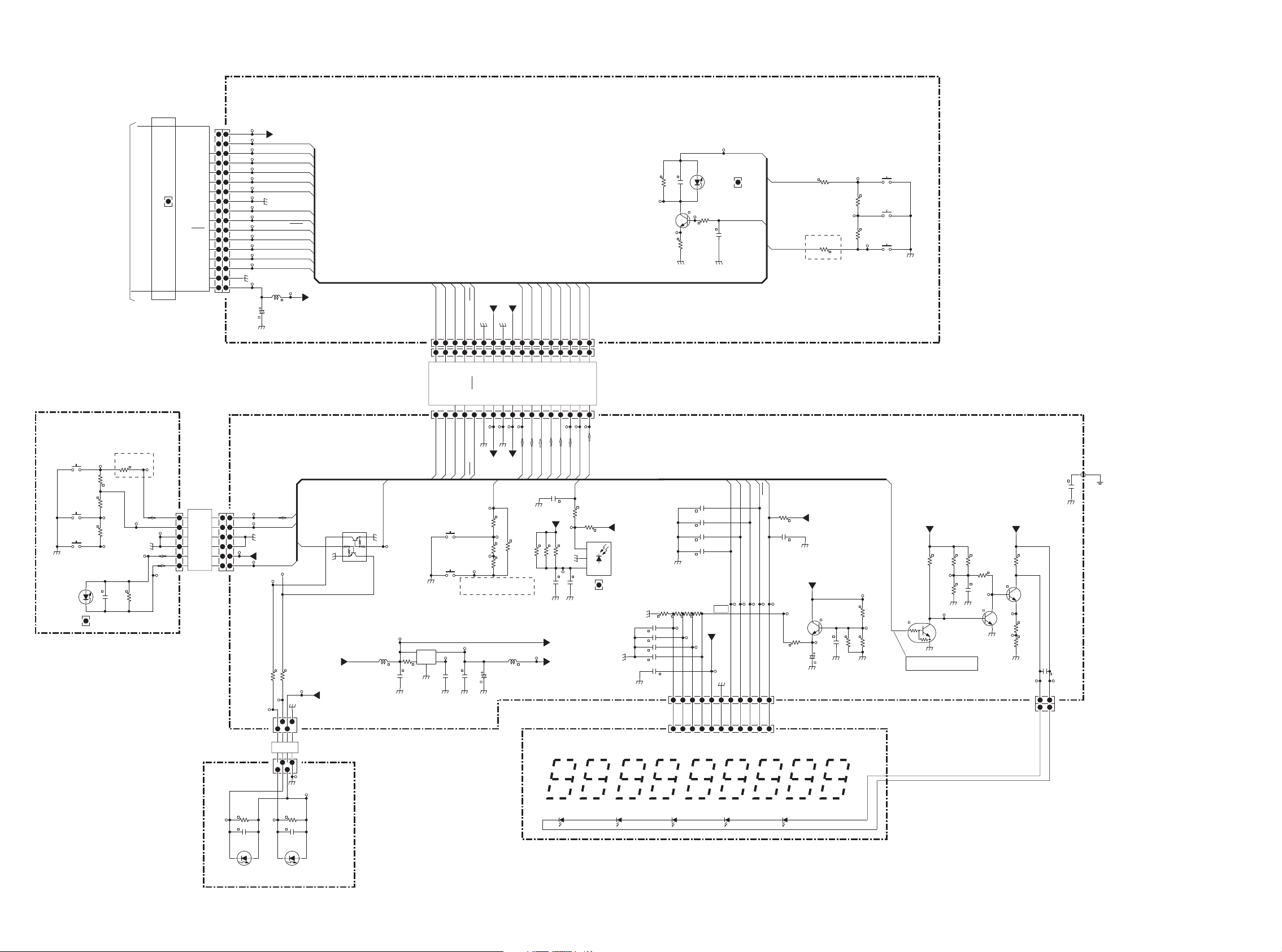
123
4
1
2
1
2
3
4
5
6
M 0116 MDL
123456789
10
11
123456789
10111213141516
17
12 12
12
12
12
12
1
2
3
4
5
6
7
8
9
10
11
12
13
14
15
16
17
1
2
3
4
5
6
7
8
9
10
11
12
13
14
15
16
17
12
1
2
3
4
5
6
7
8
9
10
11
12
13
14
15
16
17
12
1
2
3
4
5
6
1
2
3
4
5
6
12
12345
678
9
1011121314
151617
1
2
3
1110987654321
1
2
1 2 3
456
12
123
4
1
2
3 4
5
SPACER
SPACER
SPACER
NC
D_OFF
LCDOFF
KEY2
KEY3
RC5F
KEY2
S_LED
KEY1
FRES
S_OFF
FCLK
KEY3
FRES
S_LED
RC5F
FCEN
I/E_LED
KEY1
I/E _LED
FDAT
D_OFF
FDAT
LCDOFF
KEY2
KEY1
FCLK
F_RS
F_RS
FCEN
S_OFF
F_RS
S_LED
KEY3
FRES
KEY3
FCEN
KEY2
KEY1
FCEN
LCDOFF
FCLK
D_OFF
F_RS
LCDOFF
I/E_LED
FDAT
FCLK
S_LED
I/E _LED
FDAT
KEY2
RC5F
D_OFF
RC5F
KEY1
FRES
LED WIRE
10k
680
10
SMCD-17X70
SECU1E01C SML-LTT86
330
SKHVBF
SKHVBF
SKHVBF
0. 1u
0.1u0.1u
10k10k
330
17FMN-SMT
10u
NC
1. 8k
470
680
10k
0.1u
0.1u
SEL2E10C
BLU
17FMN-SMT
2.2k
2SC4081
1000p
0.47
1.8k
2SC4081
47
2. 2u
1k
0. 1u
1000p
0. 1u
1000p
1000p
NC
100
0. 1u
1. 8k
10k
SMCD-6X80
3.9k
100p
1k
0.1u
1k
22k
SKHVBF
0.47u
0.1u
2.2u
0.47u
1k
6.8k
17FMN-SMT
2SC4081
0.1u
0.47u
0.47u
0.47u
IR SENSOR
11FMN-SMT
560
2SC4081
SKHVBF
330
1k 1k
0.1u
680
1k
0.1u
100
100
22k
FERRITE CORE
0
47k
SEL2E10C
BLU
820
180
NC
470
820
390
JY08
001J
JY07
RY12
RY11
RY09
RY08
VY01
WY02
DY08 DY07
RY10
SY05
SY06
SY07
CY05
CY29CY30
RY46RY47
SY03
RY01
JY02
CY01
RY04
RY03
RY07
RY02
WY01
SY02
RY06
CY02
CY03
DY01
JY01
RY05
QY01
SY01
LY41
CY15
LY43
CY09
RY38
QY23
RY40
CY27
RY26
CY24
CY14
CY26
CY13
CY12
JY06
RY23
RY17
CY25
RY22
RY42
WY06
RY27
CY06
RY3
0
QY22
CY07
RY32
RY24
SY08
CY19
CY16
CY10
CY17
RY35
RY28
JY03
QY24
CY11
CY20
CY18
CY08
ZF01
JY09
JY04
RY36
QY21
QY11
SY09
RY19
RY33
JY05
RY31
CY21
RY37
QY25
RY39
LY42
CY22
RY16
RY18
RY25
L011
RY29
RY13
201B
203B
201B
DY02
RY20
RY21
JY10
CY31
RY41
RY44
RY43
GND
06FMN
GND
GND
GND
+5VF
SKHVBF F0052759M
+5VF
GND
GND
GND
+12VF
GN
D
SMCD-17X120
SKHVBF F0052759M
+12VF
GND
GND
GND
SKHVBF F0052759M
GND
GND
GND
GND
+12VF
GND
GND
GND
+5V
+12VF
+12VF
06FMN
+5V
GNDGND
GND
DTC114EUA
GND
3.3V
GND
GND GND
GND
GND
GND
+5V
3.3V
GND
GND
+12VF
GNDGND
GND
GND
S2B-PH-K-S
+5V
+5VF
GND
+5VF
GND
GND
GND
3.3V
UMH10NTN
GND
GND
GND
PQ1U331M2ZP
3.3V
EARTH
GND
D005
DISPLAY OFF
D002
15V
D003
LCD DISPLAY ASSY
D004
D001
KEY2
S_LED
GND
+15V
FRONT SIDE LED
GND
(LEFT)
FCEN
+15VF
S_LED
GND
D_OFF
FRES
KEY2
FCLK
KEY1
KEY3
FDAT
RC5F
LCD DISPLAY LED WIRE
15V
DAC MODE
LCDOFF
FRONT CKT(KEY,RC-5 & DISPLAY)
F_RS
KEY1
CHENG OP/CL TO PAUSE
DEL:RY06 ADD RY05(2.7K)
GND
5VF
INVERR
WY05
SUMI CARD
(RED)(BLU)
RC5F
INVERR
FDAT
KEY2
F_RS
FRES
+12VF
GND
FCLK
LCDOFF
KEY3
+5V
KEY1
S_LED
DOFF
GND
FRONT SIDE LED
FCEN
CHENG PAUSE TO OP/CL
DEL:RY03 ADD RY04(10 OHM)
(RIGHT)
KEYS(FRONT RIGHT)
FO R PA 16( J10 4)
XV
LCD BACK LIGHT LED CKT
12V
SA-15S2:DIR (RY21+RY22)
SA-13S2:INV (RY23,330)
3. 3V
XV
XV
XV
H ; LCD BACK LIGHT ON
6.2V
6.8V
XV
XV
PLAY
STOP
PAUSE
OP/CL
NEXT
PREV
SOUND
DIR
CHEG RY20(330 to 820)
RY21(680 to 180)
V4V3V1V0VDD
VSSSISCL
CSBRSXRESST
VIN
GND
VC NR
VOUT
PY26 PWB
PY36 PWB
PY46 PWB
PY16 PWB
4241
Page 37

13. PARTS LOCATION
PU16 AA PWB
C401 D3
C402 D4
C403 E3
C404 D3
C405 D2
C406 E4
C501 C6
C503 C5
C504 D5
C505 D5
C506 C5
C508 D5
C509 C5
C510 C5
C512 D5
C513 C4
C514 C4
C516 C5
C517 C5
C518 C5
C519 B5
C520 B5
C522 B5
C523 B5
C524 B5
C911 E6
C912 E5
C913 E6
C914 E6
CF01 C3
CF02 C3
CF03 C3
CF04 C2
CF05 E2
CF06 C2
CF07 C4
CF08 C4
CF09 C3
CF10 A2
CF11 A3
CF12 A2
CF13 A2
CF25 C4
J401 E2
J402 E4
J403 E5
J404 D5
J405 A1
J901 A5
JF00 E6
JF01 A3
JF04 C1
L501 D5
L502 B5
L503 C1
L504 E3
L903 E5
L904 E5
L905 E6
L906 E5
L907 E5
L908 E5
Q401 D3
Q501 C5
Q504 B5
QF01 B3
QF02 C4
QF03 C3
QF04 C2
QF05 D2
QF06 E2
R401 D2
R404 D2
R410 D3
R411 D3
R412 D3
R413 D3
R415 D3
R416 D3
R417 D3
R500 C5
R501 D6
R502 C5
R503 C6
R504 C6
R505 C5
R506 C5
R507 D5
R508 D5
R509 D5
R510 C5
R515 C5
R516 C4
R518 C5
R520 C4
R521 C4
R522 C4
R524 C5
R525 B3
R526 C5
R527 B4
R528 B4
R529 B4
R530 B4
R531 B4
R532 C4
R538 C5
R541 A3
RD60 D2
RF01 C3
RF02 D4
RF03 D4
RF04 D4
RF05 E2
RF06 D2
RF07 C2
RF08 C4
RF09 C4
RF10 C2
RF11 B2
RF12 C4
RF13 B3
RF14 D2
RF15 B3
RF16 B4
RF17 B4
RF18 B4
RF19 B2
RF20 B2
RF21 C2
RF22 C2
RF23 B2
RF25 E2
RF27 B2
RF28 B3
RF29 B3
RF30 B3
X501 C4
XF01 C3
43 44
鉛フリー半田
半田付けには、鉛フリー半田
(Sn-Ag-Cu)
を使用してください。
Lead-free Solder
When soldering, use the Lead-free Solder (Sn-Ag-Cu).
Page 38

CM02 C3
CM03 B3
CM04 B2
CM05 C5
CM06 C5
CM11 B4
CM13 C4
CM14 C4
CM15 C1
CM16 C1
JM01 B1
JM02 A4
JM03 D3
JM04 E6
JM05 C6
JM06 B6
JM08 D1
QM01 B3
QM02 B2
QM03 B2
QM04 B2
QM05 B2
QM07 C5
QM08 B4
RM04 B2
RM05 B2
RM06 B2
RM07 B3
鉛フリー半田
半田付けには、鉛フリー半田
(Sn-Ag-Cu)
を使用してください。
Lead-free Solder
When soldering, use the Lead-free Solder (Sn-Ag-Cu).
RM08 B3
RM09 B3
RM10 C5
RM12 B4
RM13 B3
RM14 B3
RM15 B3
PP16 AB PWB PF16 AA PWB
C551 B15
C552 B14
C553 B14
C554 B13
C555 C14
C556 C14
C557 C14
C558 C13
C559 C14
C560 C15
C561 C15
C565 C16
C601 D13
C602 C12
C603 D14
C604 D12
C605 C13
C607 F13
C608 J14
C609 J13
C610 F13
C611 F13
C651 D15
C652 C16
C653 C15
C654 D16
C655 C15
C657 F15
C658 J15
C659 J15
C660 F15
C661 F16
C801 G8
C802 H8
C805 I4
C811 G11
C812 F11
C813 D12
C830 F7
C831 G6
C832 H6
C833 H7
C834 G8
C835 E9
C836 E9
C851 H11
C852 K11
C853 J15
C854 J14
C855 I15
C856 I13
C901 G13
C902 H12
C915 B16
C921 G15
C922 H16
CF51 K5
CF52 K5
CF53 L5
CF54 K3
CN02 K2
CN03 I3
CN04 D9
CN05 G2
CN06 H3
CN07 K9
CN08 J5
CN09 D9
CN10 H3
CN21 K14
CT01 J7
CT02 K7
CT03 K7
CT04 K7
CT05 K7
CT06 K7
CT07 K7
CT08 K7
CT09 K6
CT10 J7
CT11 L6
CT12 K8
CT13 L8
CT14 K9
D602 E12
D603 E13
D604 D14
D605 D14
D607 E12
D608 E13
D609 E14
D610 E14
D652 E15
D653 E15
D654 D16
D655 D16
D657 E15
D658 E15
D659 E16
D660 E16
D801 G7
D802 G7
D803 G7
D804 G7
D805 F10
D806 F10
D807 G10
D808 G10
D810 E12
D811 E11
D812 E11
D821 G2
D822 G2
D823 G2
D824 G2
D831 G5
D833 G5
D851 J10
D852 J10
D853 J10
D854 I10
D855 I15
D856 I13
D857 I16
D858 I13
D861 I15
D862 I14
DF51 K4
DN01 H3
DN03 H3
DN04 G2
DN05 G3
DN06 G3
DN07 I2
DN08 I2
DN10 G2
DN11 I5
DN12 I5
DN21 K13
F811 G4
F831 G3
F832 F3
F851 E5
F852 F5
FH01 D4
G851 E5
G852 F5
GH01 D6
J501 A13
J502 A14
J503 A16
J504 B17
J604 K14
J605 K15
J609 L14
J801 F3
J803 E9
J811 G3
J812 G4
J850 F4
J851 E4
J852 E5
J853 F4
J854 F5
JF51 L5
JH01 E2
JH02 E3
JH03 D4
JH04 D5
JN01 K1
JN02 D10
JT01 L7
JT02 L6
JT03 L8
JT04 L9
JU01 L3
L101 B14
L103 B14
LF51 K5
LF52 K4
LF53 K5
LN21 K14
LT01 K6
LT04 J8
LT05 K6
LT06 K9
Q551 C14
Q601 D13
Q602 D13
Q603 D13
Q604 E13
Q605 E13
Q606 E14
Q607 E13
Q608 E13
Q609 F13
Q610 F13
Q611 E13
Q612 F12
Q613 F14
Q651 D15
Q652 D15
Q653 D15
Q654 E15
Q655 E15
Q656 E16
Q657 E16
Q658 E15
Q659 F15
Q660 F16
Q661 E16
Q662 F15
Q663 F16
Q801 I8
Q803 H4
Q811 E11
Q812 E11
Q813 E11
Q814 D11
Q815 E10
Q816 C13
Q831 I6
Q832 H5
Q833 I7
Q834 G8
Q851 I16
Q852 I12
Q853 I15
Q854 I13
Q855 I15
Q856 I13
Q901 G13
Q902 G13
Q903 G12
Q904 G14
Q921 G15
Q922 G16
Q923 G15
Q924 G16
Q925 B16
Q926 B16
QF51 K4
QF52 K3
QN01 J3
QN02 J3
QN03 J4
QN04 J4
QN05 I5
QN06 K8
QN07 I2
QN08 K8
QN09 K9
QN10 K9
QN11 I2
QT01 K7
R551 B15
R552 B15
R553 B14
R554 B14
R555 B14
R556 B14
R557 B14
R558 B14
R559 B14
R601 D13
R602 D13
R603 D13
R604 D13
R605 D14
R606 D14
R607 D12
R608 C13
R609 D13
R610 D13
R611 E13
R612 E13
R613 D13
R614 E14
R615 D13
R617 E14
R618 E13
R619 E13
R620 F12
R621 F13
R622 F13
R623 F14
R624 F13
R625 F13
R626 L14
R627 K14
R651 D16
R652 D15
R653 D16
R654 D16
R655 D15
R656 D15
R657 D16
R658 C15
R659 D16
R660 D15
R661 E15
R662 E15
R663 D16
R664 E16
R665 D16
R667 E16
R668 E15
R669 E15
R670 F15
R671 F15
R672 F16
R673 F16
R674 F15
R675 F16
R676 L15
R677 K15
R811 F11
R812 F11
R813 E11
R814 E11
R815 E12
R816 E11
R817 E11
R818 D11
R819 E11
R820 D12
R821 E10
R822 E11
R831 H5
R832 H5
R851 J15
R852 J13
R853 I15
R854 I13
R855 I16
R856 I13
R857 I15
R858 I13
R859 I15
R860 I14
R861 I15
R862 H14
R901 G13
R902 G12
R903 G13
R904 G13
R905 H13
R906 H13
R907 H13
R908 H13
R909 B16
R921 G15
R922 G15
R923 G16
R924 G15
R925 H16
R926 H15
R927 H16
R928 H16
R929 B16
RF51 K5
RF53 L4
RF54 K4
RF55 K4
RF56 L3
RF58 K3
RN01 F2
RN02 G2
RN03 H2
RN04 I3
RN05 I3
RN06 J4
RN08 I4
RN10 J9
RN11 I2
RN12 K9
RN13 K9
RN14 K9
RN15 J9
RN17 H2
RN18 B15
RN19 I2
RN21 H2
RT01 J7
RT02 K7
RT03 K7
RT04 K6
RT05 K7
RT07 K6
RT08 K8
RT09 K6
SF51 L4
SH01 D7
U1 J1
U10 F3
U100 E13
U101 K13
U102 H14
U104 G14
U105 F14
U106 C14
U107 J14
U108 B14
U109 I14
U11 F3
U110 J14
U111 H14
U112 H14
U113 I14
U114 B14
U115 C15
U116 F14
U117 G15
U118 B15
U119 D15
U12 I4
U120 H15
U121 D15
U122 A15
U123 F15
U125 E15
U126 A16
U127 H16
U128 H16
U129 F16
U13 I4
U130 A16
U131 B16
U132 L14
U133 G7
U134 K4
U135 K9
U136 F10
U137 D14
U138 C15
U139 J8
U14 I4
U140 J9
U141 H4
U142 G5
U143 G5
U144 E6
U145 C12
U15 K4
U16 K4
U17 H5
U18 G5
U19 G5
U2 H1
U20 K5
U21 J5
U22 J6
U23 I5
U24 I5
U25 H5
U26 J5
U27 J5
U28 J5
U29 J7
U3 H2
U30 H5
U31 G5
U32 H5
U33 J6
U34 G5
U36 G6
U37 G7
U38 K7
U39 H7
U4 L2
U40 H8
U41 K8
U42 J8
U43 G8
U44 C12
U45 F8
U46 E8
U47 J8
U48 H8
U49 H8
U5 I2
U50 H8
U51 J9
U52 F9
U53 G8
U54 G8
U55 G8
U56 D9
U57 F8
U58 J9
U59 F9
U6 I3
U60 F9
U61 H9
U62 H9
U63 G9
U64 G9
U65 G9
U66 K9
U67 H9
U68 F9
U69 E9
U7 I3
U70 J10
U71 F9
U72 D9
U73 J9
U74 D10
U75 G10
U76 G10
U77 E10
U78 C11
U79 D11
U8 H3
U80 E12
U81 H12
U82 C12
U83 C12
U84 K12
U85 J12
U86 J12
U87 K12
U88 F12
U89 H12
U9 K3
U90 A12
U91 B12
U92 J12
U93 B13
U94 H13
U95 B13
U96 K13
U97 C13
U98 D13
U99 F13
YH05 L16
YH06 L16
YH07 L16
YH08 L16
YH09 L16
4645
Page 39

PP16 AB PWB
鉛フリー半田
半田付けには、鉛フリー半田
Lead-free Solder
When soldering, use the Lead-free Solder (Sn-Ag-Cu).
47 48
(Sn-Ag-Cu)
を使用してください。
Page 40

PY16 AA PWB
CY06 C3
CY07 C3
CY08 C3
CY09 B4
CY10 B4
CY11 B6
CY12 B5
CY13 B5
CY14 C5
CY15 C5
CY16 B5
CY17 B5
CY18 B5
CY19 B5
CY20 B5
CY21 B7
CY22 B8
CY24 B6
CY25 B6
CY26 B6
CY27 B6
CY31 A1
JY03 B8
JY04 B7
JY05 C1
JY06 B1
JY09 B5
JY10 A1
LY42 C7
LY43 B6
QY11 C2
QY21 B4
QY22 B7
QY23 B7
QY24 B7
QY25 B6
RY13 B4
RY16 C3
RY17 C3
RY18 C3
RY19 C7
RY20 A2
RY21 A3
RY22 A3
RY23 A3
RY24 C3
RY25 B6
RY26 C3
RY27 C4
RY28 B4
RY29 B5
RY30 B5
RY31 B5
RY32 B5
RY33 B5
RY35 B7
RY36 B7
RY37 B7
RY38 B7
RY39 B7
RY40 B7
RY41 B7
RY42 B7
RY43 C1
RY44 C2
SY08 A2
SY09 A3
ZF01 C3
PY26 AA PWB PY36 AA PWB
CY01 B2
CY02 C2
CY03 C2
DY01 C1
JY01 B4
JY02 B1
LY41 B2
QY01 C1
RY01 C2
RY02 C2
RY03 B2
RY04 B2
RY05 C2
RY06 C2
RY07 C1
SY01 D3
SY02 B3
SY03 A3
CY05 B2
DY02 C3
JY07 B3
RY08 D1
RY09 D2
RY10 B1
RY11 A1
RY12 B2
SY05 D1
SY06 B1
SY07 A1
鉛フリー半田
半田付けには、鉛フリー半田
(Sn-Ag-Cu)
を使用してください。
Lead-free Solder
When soldering, use the Lead-free Solder (Sn-Ag-Cu).
5049
Page 41

PY46 AA PWB
CY29 B1
CY30 B1
DY07 B2
DY08 B2
JY08 B1
RY46 B2
RY47 B2
SUPER AUDIO CD PWB K001
PH16 AA PWB
C903 D2
C904 B2
C905 C2
C923 D2
C924 B1
C925 B2
C931 A2
C932 A2
C950 B3
C951 C3
C952 B2
C971 B2
C972 B2
J902 C3
J903 A1
J904 A2
L901 B1
L902 B1
Q951 B2
Q952 B2
Q953 C2
Q954 B2
Q971 B2
Q972 B2
Q973 B2
Q974 B2
R910 B1
R930 B1
R951 A3
R952 C2
R953 C2
R954 B2
R955 B2
R956 C2
R957 B2
R958 B3
R959 A2
R971 B2
R972 B2
R973 B2
R974 B2
R975 B2
R976 B2
R977 B2
R981 B3
51 52
鉛フリー半田
半田付けには、鉛フリー半田
(Sn-Ag-Cu)
を使用してください。
Lead-free Solder
When soldering, use the Lead-free Solder (Sn-Ag-Cu).
Page 42

A
-
+
5110
Ø3X6(M)
x6
5128
Ø3X8(M)
5146
Ø3X6(M)
5150
Ø3X8(M)
x2
5128
Ø3X8(M)x2
5128
Ø3X6(M)x4
5110
Ø3X6(M)
x2
5110
Ø3X6(M)
x4
5128
Ø3X8(M)
x2
5127
Ø3X8(M)
5129
Ø3X8(M)
x2
5148
Ø3X6(M)
x3
5126
Ø3X8(M)
x2
5146
Ø3X6(M)
5129
Ø3X8(M)
5128
Ø3X8(M)
x3
5150
Ø2X8(U)
x2
5146
Ø3X6(M)x4
5128
Ø3X4(U)
x2
5129
Ø4X10(M)
x4
5129
Ø4X10(M)
x2
5128
Ø4X8(M)
x2
5150
Ø3X8(M)
x2
5127
Ø3X8(M)x4
5128
Ø3X8(M)
x2
5128
Ø3X8(M)x2
5110
Ø3X6(M)x3
5127
Ø3X8(M)x2
5126
Ø3X10(M)
5127
Ø3X8(M)
x5
5146
Ø3X6(M)
5146
Ø3X6(M)
5148
Ø3X6(M)
5127
Ø3X8(M)
5128
Ø3X4(U)
x6
5128
Ø3X4(U)
x2
5128
Ø3X4(U)x4
5128
Ø4X20(M)x4
5128
Ø3X10(M)
x8
5129
Ø3X12(M)
x4
5127
Ø3X8(M)
x3
5128
Ø3X6(M)
x4
5127
Ø3X8(M)
5146
Ø3X6(M)
5148
Ø3X6(M)
Ø3X6(M)x2
5128
Ø3X8(M)x2
5150
Ø3X8(M)x2
5128
Ø3X8(M)
x2
5128
Ø3X8(M)
x5
5128
Ø3X8(M)
5128
Ø3X8(M)
5128
Ø3X6(M)
x3
5128
Ø2X6(U)
SYMBOL STYLE
PARTS NAME
5110
+B.H.M.SCREW
5127
+B.H.TAP TITE SCREW (W/)
5128
+B.H.TAP TITE SCREW(B TYPE)
5129
+B.H.TAP TITE SCREW(W/T.L.WASHER)
5150
+F.H.TAP TITE SCREW(B TYPE)
5126
5159
+B.H.TAP TITE SCREW W/WASHER
+B.H.TAP TITE SCREW(S TYPE)
MARK
MATERIAL/FINISH
(M) STEEL/COPPER
090B
003B
002B
001B
005B
004B
112B
5129
093B
015Bx2
076Bx2
073Bx2
058Bx2
025B
PY46
075Bx2
VY01
007Gx4
006Gx4
005Gx4
008Gx4
001D
002G
001G
080B
088Bx6
085Bx6
PY26
PY36
110B
111B
065G
001D
L002
020G
J001
070B
020B
PY16
PP16
105B
093G
PU16
031Gx2
090G
091G
W001
PH16
J203/
J204
078G
068Gx2
103Mx5
M002
002M
150B
151B
PF16
L003
023B
070Bx2
021B
099B
101B
106G
033G
035G
102G
017M
070B
085G
085G
108Gx5
009D
105D
103D
100D
103D
101D
L001
110Dx2
110Dx2
109D
N VERSION
U VERSION
070G
112Dx3
071G
118D
124D
006B
SUPER AUDIO CD TRAVERSE MECHA
M002
LOADER UNIT
M001
K001
SUPER AUDIO CD PWB
14. EXPLODED VIEW AND PARTS LIST
M002 :
Refer to 4. CAUTIONS and 7. HOW
TO THE RESET OF PLAYBACK TIME
4. CAUTIONS および 7. DISC再生時間
のリセット(初期化)方法を参照
5453
Page 43

P.W.B.
NAME
VERS.
COLOR
PART NO.
(FOR EUR)
PART NO.
(MZ)
PART NAME DESCRIPTION
001B 998402000280M 998402000280M PANEL ASSY FRONT PANEL ASSY BL SA-KI-PEARL
015B 00M32AK259100 00M32AK259100 BUSHING BUSH BUTTON BL ABS
020B 443510011005M 443510011005M CHASSIS CHASSIS MOLD BL SA-KI-PEARL
025B 416510013009M 416510013009M WINDOW WINDOW SA-15S2
POS. NO.
058B
00M32AK270010
00M32AK270010
BUTTON
BUTTON BL ABS+AL CAP
075B 00M18AK355010 00M18AK355010 LENS LENS SIDE
085B 00M04AJ259010 00M04AJ259010 BUSHING BUSH FOR FUNCTION BUTTONS BL
088B 00M04AJ270030 00M04AJ270030 BUTTON FUNCTION BUTTON BLACK
090B 00M18AK063010 00M18AK063010 ESCUTCHEON ESCUTCHEON AL L SIDE BL
093B 00M18AK063050 00M18AK063050 ESCUTCHEON ESCUTCHEON AL R SIDE BL
110B 00M18AK121010 00M18AK121010 LINK LINK POWER
111B 00M18AK112010 00M18AK112010 SHAFT SHAFT POWER
112B 00M18AK270010 00M18AK270010 BUTTON BUTTON POWER BL ABS+AL CAP
150B
418410005005M
418410005005M
ESCUTCHEON
ESCUTCHEON TRAY BL SA-KI-PEARL
151B 454510006003M 454510006003M HOLDER HOLDER ESCUTCHEON TRAY BL SA-KI-PEARL
001D 00M18AK249010 00M18AK249010 SIDE PANEL SIDE PANEL AL BL
100D 00M21AJ257020 00M21AJ257020 LID TOP COVER AL TYPE BL
005G 407410012027M 407410012027M LEG LEG ASSY SL
093G 00M10AJ154020 00M10AJ154020 KNOB KNOB HEAD PHONE AL CAP BL
001M 8M3021000202M 8M3021000202M MECHANISM SACD MECHA UNIT SA-KI-PEARL
J001 00MYJ04002640 00MYJ04002640 JACK ! R-301
(21)
AC INLET MAXES CABLE CO.LTD
J606 00MYT02011280 00MYT02011280 TERMINAL EW-2560T-LH-R
J607 00MYT02011290 00MYT02011290 TERMINAL EW-2560T-LH-W
K001 00MZK35AK0020 00MZK35AK0020 UNIT KIT DB-APB105/XJ MAIN PWB ASSY
L001
/
N1B 101010031010M 101010031010M TRANSF. # MAIN TRANSFORMER AC230V TOROIDAL
L001
/
U1B ns
p
101010031027M TRANSF. # MAIN TRANSFORMER AC120V TOROIDAL
L002 00MFC50280040 00MFC50280040 FERRITE CORE TRCN-28-16-20
L003 00MFC50230010 00MFC50230010 FERRITE CORE TFCK-23-11-14
L004 00MFC90400010 00MFC90400010 FERRITE CORE FERRITE CORE SSC-40-12
L011 00MFC90280010 00MFC90280010 FERRITE CORE HF70SH28-2-10 FPC FERRITE CORE
L012 00MFC90280010 00MFC90280010 FERRITE CORE HF70SH28-2-10 FPC FERRITE CORE
L014 00MFC50160060 00MFC50160060 FERRITE CORE FERRITE CORE TFCK-16-8-13
L801 00MFC50270040 00MFC50270040 FERRITE CORE USB-4 SLEEVE FERRITE CLAMP
L802 00MFC50270040 00MFC50270040 FERRITE CORE USB-4 SLEEVE FERRITE CLAMP
M001 311010001007M 311010001007M MECHANISM LOADER UNIT
M002 312010002010M 312010002010M MECHANISM DB-VTV736/XCN TRAVERSE
PF16 ns
pnsp
PWB ASSY DISTRIBUTE PWB ASSY
PH16 ns
pnsp
PWB ASSY HEADPHONE PWB ASSY (SA-15KI PEARL
)
PP16 ns
pnsp
PWB ASSY POWER/AUDIO PWB (SA-KI-PEARL
)
PU16 ns
pnsp
PWB ASSY MPU/DIR PWB ASSY (SA-KI-PEARL
)
PY16 ns
pnsp
PWB ASSY DISPLAY/KEY PWB ASSY
PY26
nsp
nsp
PWB ASSY
KEY1 PWB ASSY
PY36 ns
pnsp
PWB ASSY KEY2 PWB ASSY
PY46 ns
pnsp
PWB ASSY LED PWB ASSY
VY01 173010002000M 173010002000M DISPLAY LCD UNIT DP-0009-001-NR-KK
WM00 ns
p
606050046027M FPC SML2CD-24X150-BDX8(BL)-P0.5-S4-F-M-N(35
)
WM03 ns
p
606050045017M FPC SMCD-29X60-BDX10+6(BL)-P1.0-S4-M UL20624
WM05 ns
p
00MYU17070520 FPC SMCD-17X70-BDX8(BL)-P1.0-S4M
WM06 ns
p
00MYU25110520 FPC SMCD-25X110-BDX8-P1.0-S4-M
WY01 ns
p
00MYU17120520 FPC SMCD-17X120-BDX8(BL)-P1.0-S4
WY
0
2n
sp
00MYU17070520
FP
C
SMC
D-17X70-BDX8(BL)-P1.0-S4M
0sp00 U 0 05 0
C
S C 0 8( ) 0 S
WY05 ns
p
00MYU04060520 FPC 2MCD-04X60-BDX6(BL)-P1.0-S4.0
WY06 ns
p
00MYU06080520 FPC SMCD-6X80-BDX6(BL)-P1.0-S4-M UL2896
PACKING
005T 541110237033M 541110237033M USER GUIDE USER GUIDE SA-KI-PEARL
(
N/U
)
T100 307010015007M 307010015007M UNIT KIT REMOTE CONTROLLER RC003SA
W001
/
N1B 00MZC01803080 00MZC01803080 MAINS CORD # 2P MAINS CORD 10A 250V CLASS2
W001
/
U1B ns
p
00MZC01803100 MAINS CORD # MAINS CORD UL/CSA 10A 125V
NOT STANDARD SPARE PART
005S ns
p
00M31AK809010 CUSHION CUSHION FOR SET L SIDE
006S ns
p
00M31AK809020 CUSHION CUSHION FOR SET R SIDE
010S ns
p
531210081003M PACKING CASE PACKING CASE SA-KI-PEARL
015S
/
N1B ns
p
531210082006M MASS CARTON MASTER CARTON SA-KI-PEARL
J051 ns
p
00MZD00900100 CONN. CORD CINCHI CORD RC-5 0.9M
J082 ns
p
00D2032441004 CONN. CORD 2P PIN CORD
NOTE : "nsp" PART IS LISTED FOR REFERENCE ONLY, MARANTZ WILL NOT SUPPLY THESE PARTS.
55
Page 44

LOADER UNIT
P.W.B.
NAME
VERS.
COLOR
PART NO.
(FOR EUR)
PART NO.
(MZ)
PART NAME DESCRIPTION
LOADER 2 995419000010S 995419000010S TRAY TRAY
SW00-1015-00
LOADER 9 995463000020S 995463000020S GEAR MIDDLE GEAR
SW00-1009-00
LOADER 13 995462000030S 995462000030S PULLEY LOADING PULLEY(C
)
SW00-1012-00
LOADER 19 995669000040S 995669000040S SW LEAF SWITCH
SW00-3002-00
LOADER 23 995474000050S 995474000050S DUMPER INSULATOR DUMPER
SW00-4011-00
LOADER 24 995466000060S 995466000060S BELT LM BELT
SW00-4005-00
LOADER A 995684000070S 995684000070S MOTOR MOTOR ASSY (14 and 18)
SW10-3001-00
POS. NO.
24 : LM BELT
13 : LOADING PULLEY (C)
9 : MIDDLE GEAR
2 : TRAY
A : MOTOR ASSY
(14 and 18)
19 :
LEAF SWITCH
23 : INSULATOR DUMPER
NOTE : "nsp" PART IS LISTED FOR REFERENCE ONLY, MARANTZ WILL NOT SUPPLY THESE PARTS.NOTE : "nsp" PART IS LISTED FOR REFERENCE ONLY, MARANTZ WILL NOT SUPPLY THESE PARTS.
56
Page 45

15. MICROPROCESSOR AND IC DATA
QF01 : R5F212AASNFP
No.
Pin Port Mode
1 P3_3 LCD_RS I I I - LCD SELECTION REGISTER
2 P3_4 SDA I/O I/O I H IIC DATA
3 MODE MODE I I I - -
4 P4_3 IPOD_RESET I O I L
I/O
SA7003 SA8003
STBY Initial Function
IPOD ATTESTATION IC RESET OUTPUT
5 P4_4 SACD_DIR I I I L
6 RESET RESET I I I - 7 XOUT CLOCK - - - - 20MHZ
8 VSS VSS - - - - GND
9 XIN CLOCK - - - - 20MHZ
10 VCC VCC - - - - 3.3V
11 TRCIOD TRY_OPN O O I L TRAY OPEN OUTPUT PWM OUTPUT
12 TRCIOC TRY_CLS O O I L TRAY CLOSE OUTPUT PWM OUTPUT
13 P5_2 DIR_XMODE I I I L DIR RESET OUTPUT
14 P5_1 DAC_GAIN O O I L DAC GAIN CHANGE OUTPUT
15 P5_0 INVERT_LED I I I L
16 P2_7 SIDE_LED_OFF I I I L FRONT PANEL BLUE LED ON/OFF OUTPUT
17 P2_6 DIS_SO O O I H FLD/LCD DATA OUT PUT
18 P2_5 DIS_SCL O O I H FLD/LCD CLOCK OUT PUT
19 P2_4 DIS_CS O O I H FLD/LCD CHIP SELECT OUT PUT
20 P2_3 DIS_RESET O O I L FLD/LCD RESET OUT PUT
21 P2_2 IR_IN I I I - REMOTE CONTROL INPUT
22 P2_1 MOD_XDVDRST O O I L MECHANISM MODULE RESET OUTPUT
23 P2_0 MOD_XREADY O O I H MECHANISM MODULE XRDY OUTPUT
24 INT1 MOD_ACK I I I - MECHANISM MODULE ACK INPUT
25 CLK0 MOD_SCLK I I I -
26 RXD0 MOD_MDATA I I I -
27 TXD0 MOD_SDATA O O I L
28 P8_6 SACD_USB O O I L THE SIGNAL CHANGE OF USB AND SACD
29 P8_5 DAC_RESET O O I L DACRESET OUTPUT
30 P8_4 CUT_DIG O O I H DIGITAL OUT ON/OFF CONTROL
31 P8_3 AUDIO_MUTE O O I H DIGITAL OUT ON/OFF CONTROL
32 P8_2 STBY_CNT O O O H STANDBY CONTROL SIGNAL
33 P8_1 DIS_OFF O O I L DISPLAY OFF LED OUTPUT
34 P8_0 DVD_POWER O O I H
35 P6_0 IPOD_ERR I I I -
36 P4_5 LCD_LED_OFF I I I L LCD BACK LIGHT-OFF SIGNAL
37 TXD1 UART_TX O O I H FOR EXTERNAL UART COMMUNICATION
38 RXD1 UART_RX I I I - FOR EXTERNAL UART COMMUNICATION
39 CLK2 USB_SCK I O I H USB IC COMMUNICATION CLOCK INPUT
SIGNAL CHANGE OUTPUT POWER OF
SACD AND DIR
BALANCE OUTPUT POLARITY DISPLAY
LED
MECHANISM MODULE COMMUNICATION
CLOCK INPUT
MECHANISM MODULE COMMUNICATION
DATA INPUT
MECHANISM MODULE COMMUNICATION
DATA OUTPUT
MECHANISM MODULE POWER SUPPLY
CONTROL
EYE KURONASU COMMUNICATION ERROR
DETECTION
57
Page 46

58
48 47 46 45 44 43 42 41 40 39 38 37 36 35 34 33
R8C/2A Group
R8C/2B Group
17
18
19
20
21
22
23
24
25
26
27
28
29
30
31
32
1 345 6 789 10 11 12 13 14 15 162
64
63
62
61
60
59
58
57
56
55
54
53
52
51
50
49
P1_0/Kl0/AN8
P3_5/SCL/SSCK
P3_7/SSO
VCC/AVCC
VREF
P0_7/AN0/DA1
VSS/AVSS
P0_6/AN1/DA0
P0_5/AN2/CLK1
P6_1
P6_2
P0_3/AN4
P0_2/AN5
P0_0/AN7
P0_1/AN6
P0_4/AN3
P8_2/TRFO02
P2_6/TRDIOC1
P2_5/TRDIOB1
P2_4/TRDIOA1
P2_3/TRDIOD0
P2_2/TRDIOC0
P2_1/TRDIOB0
P2_0/TRDIOA0/TRDCLK
P1_7/TRAIO/INT1
P1_6/CLK0
P1_5/RXD0/(TRAIO)/(INT1)
(2)
P8_6
P8_5/TRFO12
P8_3/TRFO10/TRFI
P8_4/T
RFO11
P1_4/TXD0
P1_1/ Kl1/AN9
P8_1/ TRFO01
P8_0/ TRFO00
P6_0/ TREO
P4_5/ INT0
P6_6/ INT2/TXD 1
P6_7/ INT3/RXD 1
P6_5/ (CLK1)/C LK2
(2)
P6_4/ RXD2
P6_3/ TXD2
P3_1/ TRBO
P3_6/ (INT1)
(2)
P3_2/ (INT2)
(2)
P1_2/ Kl2/AN10
P1_3/ Kl3/AN11
P3_0/ TRAO
P3_3/ SSI
P2_7/ TRDIOD1
P5_0/ TRCCLK
P5_1/ TRCIOA/T RCTRG
P5_2/ TRCIOB
P5_3/ TRCIOC
P5_4/ TRCIOD
VCC/AV CC
P4_6/ XIN
VSS/AV SS
P4_7/ XOUT
(1)
P4_4/ XCOUT
P4_3/ XCIN
P3_4/ SDA/SCS
MODE
RESE T
NOTES:
1. P4_7/XOUT are an input-only port.
2. Can be assigned to the pin in parentheses by a program.
3. Confirm the pin 1 position on the package by referring t
o the package dimensions.
PLQP0064KB-A(64P6Q-A)
PLQP0064GA-A(64P6U-A)
(top view)
D/A converter
(8 bits
× 2)
R8C/Tiny Series CPU core
Memory
ROM
(1)
RAM
(2)
Multiplier
R0H R0L
R1H
R2
R3
R1L
A0
A1
FB
SB
USP
ISP
INTB
PC
FLG
I/O ports
NOTES:
1. ROM size varies with MCU type.
2. RAM size varies with MCU type.
8
Port P1
8
Port P3
3 2
Port P4
8
Port P0
8
Por t P2
5
Port P5
System clock
generation circuit
XIN-XOUT
High-speed on-chip oscillator
Low-speed on-chip oscillator
XCIN-XCOUT
Timers
Timer RA (8 bits × 1)
Timer RB (8 bits × 1)
Timer RC (16 bits × 1 )
Timer RD (16 bits × 2)
Timer RE (8 bits × 1)
Timer RF (16 bits × 1)
UART or
clock synchronous serial I/O
(8 bits × 3)
I2C bus or SSU
(8 bits × 1)
Peripheral functions
Watchdog timer
(15 bits)
A/D converter
(10 bits
× 12 channels)
LIN module
8
Port P6
7
Port P 8
QF01 : R5F212AASNFP
No.
Pin Port Mode
I/O
SA7003 SA8003
STBY Initial Function
40 RXD2 USB_SI I I I - USB IC COMMUNICATION DATA INPUT
41 TXD2 USB_SO I O I H USB IC COMMUNICATION DATA OUTPUT
42 P3_1 USB_RTS I O I H
USB IC COMMUNICATION REQUEST
OUTPUT
43 P3_0 USB_RESET I O I L USB IC RESET OUTPUT
44 P3_6 USB_STBY_B I O I H USB IC STANDBY CONTROL OUTPUT
45 INT2 USB_CTS I I I - USB IC COMMUNICATION REQUEST INPUT
46 KI3 USB_DDI I I I - USB IC ERROR DETECTION
47 KI2 DIR_INT I I I - DIR IC INTERRUPT REQUEST INPUT
48 KI1 STB_IR I I I - STANDBY RETURN INPUT
49 KI0 POWER_DET I I I - POWER DOWN DETECTION
50 AN7 KEY_1 I I I - KEY INPUT AD INPUT
51 AN6 KEY_2 I I I - KEY INPUT AD INPUT
52 AN5 KEY_3 I I I - KEY INPUT AD INPUT
53 AN4 TRAY_IN_SW I I I -
TRAY OPEN CLOSING TRIGGER INPUT
AD INPUT
54 P0_4 DIR_DO I I I L DIR IC DATA OUTPUT
55 P6_2 DIR_DI I I I - DIR IC DATA INPUT
56 P6_1 DIR_CL I I I L DIR IC CLOCK OUTPUT
57P0_5
_CE I I I L DIR IC CHIP ENABLE OUTPUT
DIR
58 AN1 MODEL_SEL_1 I I I - MODEL SELECTION AD INPUT
59 VSS VSS - - - - GND
60 AN0 MODEL_SEL_2 I I I - MODEL SELECTION AD INPUT
61 VREF VREF - - - - 3.3V
62 VCC VCC - - - - 3.3V
63 P3_7 USB_NMI I I I - USB IC STANDBY DETECTION
64 P3_5 SCL O O I H IIC CLOCK OUTPUT
Page 47
59
MAX 3000A Programmable Logic Device Family Data Sheet
6 or 10
6 or 10
INPUT/GCLRn
6 or 10 Output Enables
(1)
6 or 10 Output Enables
(1)
16
36 36
16
I/O
Control
Block
LAB C
LAB D
I/O
Control
Block
6 or 10
16
36 36
16
I/O
Control
Block
LAB A
Macrocells
1 to 16
LAB B
I/O
Control
Block
6 or 10
PIA
INPUT/GCLK1
INPUT/OE2/GCLK2
INPUT/OE1
2 to 16 I/O
2 to 16 I/O
2 to 16 I/O
2 to 16 I/O
2 to
16
2 to
16
2 to
16
2 to
16
2 to 16
2 to 16
2 to 16
2 to 16
Macrocells
17 to 32
Macrocells
33 to 48
Macrocells
49 to 64
Q401 : EPM3032A (Programmable Logic Device)
Pin Name Name/Usage Pin No. Dir. I/O Standard Voltage User Assignment
TDI TDI 1 input 3.3-V LVTTL N For PLD writing
SEL2 RESERVED_INPUT 2 SEL
NC RESERVED_INPUT 3 NC
GNDIO GND 4 gnd GND
SYCL SMLCK 5 output 3.3-V LVTTL Y Master Clock output
LRCK/SAR SWCLK 6 output 3.3-V LVTTL Y Word Clock output
TMS TMS 7 input 3.3-V LVTTL N For PLD writing
BCK/SACK SBCLK 8 output 3.3-V LVTTL Y Bit Clock output
VCC VCCIO 9 power 3.3V Power
SDAT/SAL SDATA 10 output 3.3-V LVTTL Y Audio Data output
GND GND 11 gnd GND
DIRINT/EMPH EMP_FLG 12 output 3.3-V LVTTL Y DAIR interrupt request output
USB/CD CD_USB 13 input 3.3-V LVTTL Y SA-CD&CD/USB change signal input
SA/DIR CD_DIR 14 input 3.3-V LVTTL Y SA-CD&CD/DAIR change signal input
DIRMCK DAIR_MCLK 15 input 3.3-V LVTTL Y DAIR Master Clock input
GNDINT GND 16 gnd GND
VCC VCCINT 17 power 3.3V Power
DIRBCK DAIR_BCLK 18 input 3.3-V LVTTL Y DAIR Bit Clock input
DIRLR DAIR_WCLK 19 input 3.3-V LVTTL Y DAIR Word Clock input
DIRDAT DAIR_DATA 20 input 3.3-V LVTTL Y DAIR Audio Data input
SA/PCM CD_SACD 21 input 3.3-V LVTTL Y CD/SA-CD change signal input
USBMCK USB_MCLK 22 input 3.3-V LVTTL Y USB Master Clock input
USBSCLK USB_BCLK 23 input 3.3-V LVTTL Y USB Bit Clock input
GND GND 24 gnd GND
USBDAT USB_DATA 25 input 3.3-V LVTTL Y USB Audio Data input
TCK TCK 26 input 3.3-V LVTTL N For PLD writing
USBLR USB_WCLK 27 input 3.3-V LVTTL Y USB Word Clock input
MCLK CD_MCLK 28 input 3.3-V LVTTL Y SA-CD Module Master Clock input
VCC VCCIO 29 power 3.3V Power
GND GND 30 gnd GND
MLRCK CD_WCLK 31 input 3.3-V LVTTL Y SA-CD Module Word Clock input
TDO TDO 32 output 3.3-V LVTTL N For PLD writing
MSDAT CD_DATA 33 input 3.3-V LVTTL Y SA-CD Module Audio Data input
MDATR MOD_DATAR 34 input 3.3-V LVTTL Y SA-CD Module DSD Rch Data input
MBCL CD_BCLK 35 input 3.3-V LVTTL Y SA-CD Module Bit Clock input
GND GND 36 gnd GND
CS 37 D_CS2, SA-CD Module K001 PWB
SO 38 D_SO, SA-CD Module K001 PWB
NC 39 NC
SC 40 D_SCLK, SA-CD Module K001 PWB
VCC VCCINT 41 power 3.3V Power
NC RESERVED_INPUT 42 NC
DIRINT_IN DIR_INT_I 43 input 3.3-V LVTTL Y DAIR interrupt request output
SEL1 RESERVED_INPUT 44 SEL
Page 48

60
LC89057W-VF4
39
38
37
DI
RERR
SLRCK
SDIN
DO
36
42
41
40
45
44
43
48
47
46
CL
CE
DGND
XMODE
TMCK/PIO0
DV
DD
TLRCK/PIO2
TBCK/PIO1
TXO/PIOEN
TDATA/PIO3
INT
35
CKST
34
A
UDIO/VO
33 32 31
LC89057W-VF4
DV
DD
30
XIN
29
EMPHA/UO
DGND
28 27
DV
DD
26
DV
DD
DGND
DGND
25
XOUT
XMCK
23
24
2 1
RDATA
SBCK
DVDD
RLRCK
RBCK
DGND
A
GND
RMCK
LPF
A
VDD
* RX5/VI
* RX6/UI
* : Pull-down resistor internal
DV
DD
* RX4
* RX3
DGND
RX1
* RX2
RXOUT
* RX0
4 3 65 87 109 1211
21
22
19
20
17
18
15
16
13
14
LC89057W-VF4
XMCKXIN XOUT
XMODECICECLINTAUDIO/VOEMPHA/UO
RXOUT
CKST
Demodulation
&
Lock detect
Modulation
or
Parallel Port
Data
Selector
Clock
Selector
Microcontroller
I/F
1/N
PLL
Cbit, Ubit
Input
Selector
RX0
RX1
RX2
RX3
RX4
RX5/VI
TBCK/PIO1
TMCK/PIO0
RMCK
RBCK
SDIN
RDATA
RERR
DO
LPF
RX6/UI
TXO/PIOEN
TDATA/PIO3
TLRCK/PIO2
RLRCK
SBCK
SLRCK
1
10
9
8
5
4
3
2
13
44
45
46
47
48
3332 35 48 39 38 41
21
37
36
22
23
20
17
16
24
29 28 27 34
Q501 : LC89057W-VF4
Page 49

61
LC89057W-VF4
5. Pin Functions
Table 5.1 Pin Functions
Pin No. Name I/O Function
1 RXOUT O
Output pin of Input bi-phase selection data
2 RX0 I5
Input pin of TTL-compatible digital data
3 RX1 I
Digital data input pin with built-in amplifier that supports coaxial
4 RX2 I5
Input pin of TTL-compatible digital data
5 RX3 I5
Input pin of TTL-compatible digital data
6 DGND
Digital GND
7 DVDD
Digital power supply
8 RX4 I5
Input pin of TTL-compatible digital data
9 RX5/VI I5
TTL-compatible digital data || Validity flag input pin for modulation
10 RX6/UI I5
TTL-compatible digital data || User data input pin for modulation
11 DVDD
Digital power supply for PLL
12 DGND
Digital GND for PLL
13 LPF O
PLL loop filter connection pin
14 AVDD
Analog power supply for PLL
15 AGND
Analog GND for PLL
16 RMCK O
R system clock output pin (256fs, 512fs, XIN, VCO)
17 RBCK O/I
R bit clock input/output pin (64fs)
18 DGND
Digital GND
19 DVDD
Digital power supply
20 RLRCK O/I
R LR clock input/output pin (fs)
21 RDATA O
Output pin of serial audio data
22 SBCK O
S bit clock output pin (32fs, 64fs, 128fs)
23 SLRCK O
S LR clock output pin (fs/2, fs, 2fs)
24 SDIN I5
Input pin of serial audio data
25 DGND
Digital GND
26 DVDD
Digital power supply
27 XMCK O
Oscillation amplifier output pin
28 XOUT O
Quartz resonator connection output pin
29 XIN I
Quartz resonator connection, input pin of external supply clock (24.576 MHz or 12.288 MHz)
30 DVDD
Digital power supply
31 DGND
Digital GND
32 EMPHA/UO I/O
Emphasis information || U data output || Chip address setting pin
33
______
AUDIO/VO I/O
Non-PCM detection || V flag output || Chip address setting pin
34
_____
CKST I/O
Output of clock switch transitional period signal || Demodulation master or slave function switch pin
35
___
INT I/O
Interrupt output for Microcontroller (Possible to select an interrupt factor.) || Modulation or general-purpose
I/O switch pin
36 RERR O
PLL clock error, data error flag output
37 DO O
Microcontroller I/F, read data output pin (3-state)
38 DI I5
Microcontroller I/F, write data input pin
39 CE I5
Microcontroller I/F, chip enable input pin
40 CL I5
Microcontroller I/F, clock input pin
41 XMODE I5
System reset input pin
42 DGND
Digital GND
43 DVDD
Digital power supply
44 TMCK/PIO0 I/O
256fs system clock input for modulation || General-purpose I/O input/output pin
45 TMCK/PIO1 I/O
64fs bit clock input for modulation || General-purpose I/O input/output pin
46 TLRCK/PIO2 I/O
fs clock input for modulation || General-purpose I/O input/output pin
47 TLRCK/PIO3 I/O
serial audio data input for modulation || General-purpose I/O input/output pin
48 TXO/PIOEN O/I
Modulation data output || General-purpose I/O enable input pin
1) Withstand voltage input/output: I or O = −0.3 to 3.6V, I5= −0.3 to 5.5V
2) Pins 32 and 33 are input pins for chip address setting, when pin 41 = "L".
3) Pin 34 is a demodulation function master or an input pin for slave setting, when pin 41 = "L".
4) Pin 35 is a modulation function or an input pin for general-purpose I/O function switch setting, when pin 41 = "L".
5) ON/OFF for all power supplies must be done at the same timing as a latch-up countermeasure.
Q501 : LC89057W-VF4
Page 50
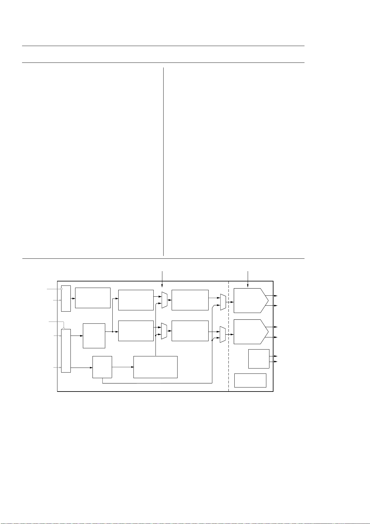
62
120 dB, 192 kHz Multi-Bit DAC with Volume Control
Features
Advanced Multi-bit Delta-Sigma Architecture
– 120 dB Dynamic Range
– -107 dB THD+N
– Low Clock Jitter Sensitivity
– Differential Analog Outputs
PCM input
– 102 dB of Stopband Attenuation
– Supports Sample Rates up to 192 kHz
– Accepts up to 24 bit Audio Data
– Supports All Industry Standard Audio
Interface Formats
– Selectable Digital Filter Response
– Volume Control with 1/2 dB Step Size and
Soft Ramp
– Flexible Channel Routing and Mixing
– Selectable De-Emphasis
Supports Stand-Alone or I²C/SPI™
Configuration
Embedded Level Translators
– 1.8 V to 5 V Serial Audio Input
– 1.8 V to 5 V Control Data Input
Direct Stream Digital (DSD)
– Dedicated DSD Input Pins
– On-Chip 50 kHz Filter to Meet Scarlet Book
SACD Recommendations
– Matched PCM and DSD Analog Output
Levels
– Non-Decimating Volume Control with
1/2 dB Step Size and Soft Ramp
– DSD Mute Detection
– Supports Phase-Modulated Inputs
– Optional Direct DSD Path to On-Chip
Switched Capacitor Filter
Control Output for External Muting
– Independent Left and Right Mute Controls
– Supports Auto Detection of Mute Output
Polarity
Typical Applications
– DVD Players
– SACD Players
– A/V Receivers
– Professional Audio Products
PCM
Serial
Interface
Multibit
∆Σ Modulator
Interpolation
Filter with
Volume Control
Internal Voltage
Reference
External
Mute
Control
Swit ched
Capacit or
DAC and
Filter
DSD
Interface
PCM Input
Left and Ri ght
Mute Controls
Right
Differenti al
Output
Left
Differenti al
Output
DSD Input
DSD Processor
1.8 V to 5V
1.8 V to 5 V
-Volume cont rol
-50kHz filter
Swit ched
Capacit or
DAC and
Filter
MU X
Dire ct DSD
Le vel Tran slato r
Le vel
Tra nsla tor
Hardware or I2C/SPI
Control Data
MU X
Multibit
∆Σ
Modulator
Interpolation
Filter with
Volume Control
MU X
MU X
3.3 V to 5 V 5 V
Register/Hardware
Configuration
CS4398
Q551 : CS4398
Page 51

63
CS4398
DSD_B DSD_A
DSD_SCLK VLS
SDIN VQ
SCLK AMUTEC
LRCK AOUTA-
MCLK AOUTA+
VD VA
DGND AGND
M3 (AD1/CDIN) AOUTB+
M2 (SCL/CCLK) AOUTB-
M1 (SDA/CDOUT) BMUTEC
M0 (AD0/CS) VREF
RST REF_GND
VLC FILT+
1
2
3
4
5
6
7
8 21
22
23
24
25
26
27
28
9
10
11
12 17
18
19
20
13
14 15
16
CS4398
Pin Name Pin # Pin Description
DSD_A
DSD_B
28
1
Direct Stream Digital Input (Input) - Input for Direct Stream Digital serial audio data.
DSD_SCLK 2 DSD Serial Clock (Input) - Serial clock for the Direct Stream Digital audio interface.
SDIN 3 Serial Audio Data Input (Input) - Input for two’s complement serial audio data.
SCLK 4 Serial Clock (Input) - Serial clock for the serial audio interface.
LRCK 5
Left Right Clock (Input) - Determines which channel, Left or Right, is currently active on
the serial audio data line.
MCLK 6 Master Clock (Input) - Clock source for the delta-sigma modulator and digital filters.
VD 7 Digital Power (Input) - Positive power for the digital section.
DGND 8 Digital Ground (Input) - Ground reference for the digital section.
RST 13 Reset
(Input) - The device enters system reset when enabled.
VLC 14 Control Port Power (Input) - Positive power for Control Port I/O.
FILT+ 15
Positive Voltage Reference (Output) - Positive reference voltage for the internal sampling circuits.
REF_GND 16 Reference Ground (Input) - Ground reference for the internal sampling circuits.
VREF 17 Voltage Reference (Input) - Positive voltage reference for the internal sampling circuits.
BMUTEC
AMUTEC
18
25
Mute Control (Output) - The Mute Control pin is active during power-up initialization, mut-
ing, power-down or if the master clock to left/right clock frequency ratio is incorrect. During
reset, these outputs are set to a high impedance.
AOUTB+
AOUTB-
2019Differential Right Channel Analog Output (Output) - The full-scale differential analog
output level is specified in the Analog Characteristics specification table.
AGND 21 Analog Ground (Input) - Ground reference for the analog section.
VA 22 Analog Power (Input) - Positive power for the analog section.
AOUTA+
AOUTA-
2324Differential Left Channel Analog Output (Output) - The full-scale differential analog out-
put level is specified in the Analog Characteristics specification table.
VQ 26 Quiescent Voltage (Output) - Filter connection for internal quiescent voltage.
VLS 27 Serial Audio Interface Power (Input) - Positive power for serial audio interface I/O.
Stand-Alone Mode Definitions
M3
M2
M1
M0
9
10
11
12
Mode Selection (Input) - Determines the operational mode of the device.
Control Port Mode Definitions
AD1/CDIN 9
Address Bit 1 (I²C) / Control Data Input (SPI) (Input) - AD1 is a chip address pin in I²C
mode; CDIN is the input data line for the Control Port interface in SPI mode.
SCL/CCLK 10 Serial Control Port Clock (Input) - Serial clock for the serial Control Port.
SDA/CDOUT 11
Serial Control Data (I²C) / Control Data Output (SPI) (Input/Output) - SDA is a data I/O
line in I²C mode. CDOUT is the output data line for the Control Port interface in SPI mode.
AD0/CS
12
Address Bit 0 (I²C) / Control Port Chip Select (SPI) (Input) - AD0 is a chip address pin
in I²C mode; CS
is the chip select signal for SPI format.
Q551 : CS4398
Page 52

16. ELECTRICAL PARTS LIST
PARTS INFORMATION
RESISTORS
1) 00MGD05
2) 00MGD05
Examples ;
Resistance value
➀
0.1Ω ....001 10Ω ....100 1kΩ .... 102 100kΩ .... 104
0.5Ω ....005 18Ω ....180 2.7kΩ .... 272 680kΩ .... 684
1Ω ....010 100Ω ....101 10kΩ .... 103 1MΩ .... 105
6.8Ω ....068 390Ω ....391 22kΩ .... 223 4.7MΩ .... 475
Note : Please distinguish 1/4W from 1/6W by the shape of parts
used actually.
CAPACITORS
CERAMIC CAP.
3) 00MDD1 × × × × 370, Ceramic capacitor
Disc type
Temp.coeff.P350~N1000, 50V
Examples ;
Tolerance (Capacity deviation)
➁
±0.25pF ......0
±0.5pF ......1
±5% ......5
Tolerance of COMMON PARTS handled here are as follows :
✽
0.5pF~ 5pF .... ±0.25pF
6pF~ 10pF .... ±0.5pF
12pF~ 560pF .... ±5%
Capacity value
➂
0.5pF .... 005 3pF ....030 100pF .... 101
1pF .... 010 10pF ....100 220pF .... 221
1.5pF .... 015 47pF ....470 560pF .... 561
140, Carbon film fixed resistor, ±5% 1/4W
× × ×
160, Carbon film fixed resistor, ±5% 1/6W
× × ×
}
Resistance value
➀
}
➁ ➂
Capacity value
Tolerance
NOTE ON SAFETY FOR FUSIBLE RESISTOR :
The suppliers and their type numbers of fusible resistors
are as follows;
1. KOA Corporation
Part No. (MJI) Type No. (KOA) Description
00MNH05 × × × 140 RF25S × × × × ΩJ (±5% 1/4W)
00MNH05 × × × 120 RF50S × × × × ΩJ (±5% 1/2W)
00MNH85 × × × 110 RF73B2A × × × × ΩJ (±5% 1/10W)
00MNH95 × × × 140 RF73B2E × × × × ΩJ (±5% 1/4W)
2. Matsushita Electronic Components Co., Ltd
Part No. (MJI) Type No. (MEC) Description
00MNF05 × × × 140 ERD-2FCJ × × × (±5% 1/4W)
00MRF05 × × × 140
00MNF02 × × × 140
00MRF02 × × × 140
Examples ;
0.1Ω ....001 10Ω ....100 1kΩ .... 102 100kΩ ....104
0.5Ω ....005 18Ω ....180 2.7kΩ .... 272 680kΩ ....684
1Ω ....010 100Ω ....101 10kΩ .... 103 1MΩ ....105
6.8Ω ....068 390Ω ....391 22kΩ .... 223 4.7MΩ ....475
}
✽
}
Resistance value
*
▲▲
▲ ▲
Resistance value
▲ ▲
ERD-2FCG
Resistance value
✽
}
Resistance value
(0.1 − 10kΩ)
× × × (±2% 1/4W)
}
Resistance value
✽
ABBREVIATION AND MARKS
CERAMIC CAP.
4) 00MDK16
Examples ;
Capacity value
➃
100pF .... 101 1000pF .... 102 10000pF ....103
470pF .... 471 2200pF .... 222
ELECTROLY CAP. ( )
5) 00MEA
Examples ;
Capacity value
➄
0.1µF.....104 4.7µF ....475 100µF ... 107
0.33µF.....334 10µF ....106 330µF ... 337
1µF.....105 22µF ....226 1100µF ... 118
2200µF ... 228
Working voltage
➅
6.3V.....006 25V ....025
10V.....010 35V ....035
16V.....016 50V ....050
FILM CAP. ( )
6) 00MDF15
00MDF15
00MDF16
Examples ;
Capacity value
➆
0.001µF (1000pF) ......... 102 0.1µF .... 104
0.0018µF......................... 182 0.56µF .... 564
0.01µF......................... 103 1µF .... 105
0.015µF.........................153
}
300, High dielectric constant ceramic
× × ×
capacitor
➃
Disc type
Temp.chara. 2B4, 50V
× × × × ×
}
One-way lead type, Tolerance ±20%
➄ ➅
× × ×
× × ×
× × ×
}
One-way type, Mylar ±10% 50V
➆
Capacity value
10, Electrolytic capacitor
}
×
Working voltage
Capacity value
350 Plastic film capacitor
310 One-way type, Mylar ±5% 50V
310 Plastic film capacitor
▲
▲
Capacity value
ANT. : ANTENNA BATT. : BATTERY
CAP. : CAPACITOR CER. : CERAMIC
CONN. : CONNECTING DIG. : DIGITAL
HP : HEADPHONE MIC. : MICROPHONE
µ-PRO : MICROPROCESSOR REC. : RECORDING
RES. : RESISTOR SPK : SPEAKER
SW : SWITCH
TRIM. : TRIMMING TRS. : TRAMSISTOR
VAR. : VARIABLE X’TAL : CRYSTAL
TRANSF.
: TRANSFORMER
NOTE ON FUSE :
Regarding to all parts of parts code 00MFS20xxx2xx, replace
only with Wickmann-Werke GmbH, Type 372 non glass type
fuse.
NOTE ON SAFETY :
Symbol Fire or e lectr ical shoc k hazard. Only original
part s shoul d be us e d t o repl a c e d any pa r t m ar ke d with
symbol . A n y other co m po ne nt subst i t u ti o n (other
th a n origina l type), may incre a se risk of fire o r electri c al
shock hazard.
安全上の注意 :
がついている部品は、安全上重要な部品です。必ず
指定されている部品番号の部品を使用して下さい。
64
060522 MZ
Page 53

P.W.B.
NAME
VERS.
COLOR
PART NO.
(FOR EUR)
PART NO.
(MZ)
PART NAME DESCRIPTION
DISTRIBUTE PWB PF16
(
00MWG35AK207-
)
PF16 CM02 00MEY47600620 00MEY47600620 ELECT CAP. 47UF/6.3V
PF16 CM03 ns
p
00MDK98104200 CER. CAP. GRM39F104Z16 0.1UF
PF16 CM04 00MEY10601620 00MEY10601620 ELECT CAP. 10UF/ 16V
POS. NO.
PF16
CM05
00MEY47600620
00MEY47600620
ELECT CAP
.
47UF/6.3V
PF16 CM06 ns
p
00MDK98104200 CER. CAP. GRM39F104Z16 0.1UF
PF16 CM11 ns
p
00MDK98104200 CER. CAP. GRM39F104Z16 0.1UF
PF16 CM13 ns
p
00MDK98104200 CER. CAP. GRM39F104Z16 0.1UF
PF16 CM14 ns
p
00MDK98104200 CER. CAP. GRM39F104Z16 0.1UF
PF16 CM15 ns
p
00MDK96102300 CER. CAP. 1000 PF +-10% B 50V GR36
PF16 CM16 ns
p
00MDK98104200 CER. CAP. GRM39F104Z16 0.1UF
PF16 QM01 232710014509S 232710014509S IC BD7931F-E2
PF16 QM02 00MBA12303000 00MBA12303000 TRS. DTA124EU RN2303 UMT TYPE
PF16
QM03
00MBA12303000
00MBA12303000
TRS.DTA124EU RN2303 UMT TYPE
PF16 QM04 00MBA21303000 00MBA21303000 TRS. DTC124EU RN1303 UMT TYPE
PF16 QM05 00MBA21303000 00MBA21303000 TRS. DTC124EU RN1303 UMT TYPE
PF16 QM07 00MHC008305K0 00MHC008305K0 IC TC7WH241FU
PF16 QM08 00MHC96303320 00MHC96303320 IC PQ1U331M2ZPH 3.3V 300MA
PF16 RM04 ns
p
00MNN05102610 CHIP RES. 1K OHM +-5% 1/16W
PF16 RM05 ns
p
00MNN05102610 CHIP RES. 1K OHM +-5% 1/16W
PF16 RM06 ns
p
00MNN05222610 CHIP RES. 2.2K OHM +-5% 1/16W
PF16 RM07 ns
p
00MNN05392610 CHIP RES. 3.9K OHM +-5% 1/16W
PF16 RM08 ns
p
00MNN05392610 CHIP RES. 3.9K OHM +-5% 1/16W
p
PF16 RM09 ns
p
00MNN05153610 CHIP RES. 15K OHM +-5% 1/16W
PF16 RM10 ns
p
00MNN05470610 CHIP RES. 47 OHM +-5% 1/16W
PF16 RM12 ns
p
00MNN05472610 CHIP RES. 4.7K OHM +-5% 1/16W
PF16 RM13 ns
p
00MNN05102610 CHIP RES. 1K OHM +-5% 1/16W
PF16 RM14 ns
p
00MNN05102610 CHIP RES. 1K OHM +-5% 1/16W
HEADPHONE PWB PH16
(
00MWG35AK206-
)
PH16 C903 00MEY47601620 00MEY47601620 ELECT CAP. 47UF/ 16V
PH16 C904 ns
p
00MDK96102300 CER. CAP. 1000 PF +-10% B 50V GR36
PH16 C905 ns
p
00MOA476025R0 ELECT CAP. ROA-25V 470M -G3# - T2
PH16 C923 00MEY47601620 00MEY47601620 ELECT CAP. 47UF/ 16V
PH16 C924 ns
p
00MDK96102300 CER. CAP. 1000 PF +-10% B 50V GR36
PH16 C925 ns
p
00MOA476025R0 ELECT CAP. ROA-25V 470M -G3# - T2
PH16 C931 ns
p
00MDK96102300 CER. CAP. 1000 PF +-10% B 50V GR36
PH16 C932 ns
p
00MDK98104200 CER. CAP. GRM39F104Z16 0.1UF
PH16 C950 00MEY10601620 00MEY10601620 ELECT CAP. 10UF/ 16V
PH16 C951 ns
p
00MDK98104200 CER. CAP. GRM39F104Z16 0.1UF
PH16 C952 ns
p
00MDK96221300 CER. CAP. 220PF (GR39
)
PH16 C971 00MEY10601620 00MEY10601620 ELECT CAP. 10UF/ 16V
PH16
C972
nsp
00MDK96221300
CER. CAP
.
220PF (GR39)
PH16 J903 6430100020040 6430100020040 TERMINAL YKB21-5805 (BLK/SIL) HEADPHONE JACK
PH16 L901 00MFC90020100 00MFC90020100 FERRITE CORE FB M J2125HM330-T
PH16 L902 00MFC90020100 00MFC90020100 FERRITE CORE FB M J2125HM330-T
PH16 Q951 00MHX115862A0 00MHX115862A0 CHIP TRS. ! 2SA1586
(
O Y
)
PH16 Q952 00MHX341162B0 00MHX341162B0 CHIP TRS. ! 2SC4116
PH16 Q953 00MHX341162B0 00MHX341162B0 CHIP TRS. 2SC4116
PH16 Q954 00MHX115862A0 00MHX115862A0 CHIP TRS. 2SA1586
(
O Y
)
PH16 Q971 00MHX115862A0 00MHX115862A0 CHIP TRS. 2SA1586 (O Y
)
PH1
6
Q97200
MHX341162B
0
00
MHX341162B
0
C
HIP TRS.2
SC
411
6
6Q900 3 6 0
00 3 6 0
CS
SC 6
PH16 Q973 00MHX341162B0 00MHX341162B0 CHIP TRS. 2SC4116
PH16 Q974 00MHX115862A0 00MHX115862A0 CHIP TRS. 2SA1586
(
O Y
)
PH16 R910 ns
p
00MNN05473610 CHIP RES. 47K OHM +-5% 1/16W
PH16 R930 ns
p
00MNN05473610 CHIP RES. 47K OHM +-5% 1/16W
PH16 R951 00D2115646001 00D2115646001 VAR. RES. V092Q20FA103
(
METAL
)
PH16 R952 ns
p
00MNN05560610 CHIP RES. 56 OHM +-5% 1/16W
PH16 R953 ns
p
00MNN05562610 CHIP RES. 5.6K OHM +-5% 1/16W
PH16 R954 ns
p
00MNN05560610 CHIP RES. 56 OHM +-5% 1/16W
PH16 R955 ns
p
00MNN05562610 CHIP RES. 5.6K OHM +-5% 1/16W
PH16 R956 ns
p
00MNN05470610 CHIP RES. 47 OHM +-5% 1/16W
PH16 R957 ns
p
00MNN05470610 CHIP RES. 47 OHM +-5% 1/16W
PH16 R958 ns
p
00MNN05104610 CHIP RES. 100K OHM +-5% 1/16W
PH16 R959 ns
p
00MNN05104610 CHIP RES. 100K OHM +-5% 1/16W
PH16 R971 ns
p
00MNN05471610 CHIP RES. 470 OHM +-5% 1/16W
PH16 R972 ns
p
00MNN05560610 CHIP RES. 56 OHM +-5% 1/16W
PH16 R973 ns
p
00MNN05562610 CHIP RES. 5.6K OHM +-5% 1/16W
NOTE : "nsp" PART IS LISTED FOR REFERENCE ONLY, MARANTZ WILL NOT SUPPLY THESE PARTS.
65
Page 54

66
NOTE : "nsp" PART IS LISTED FOR REFERENCE ONLY, MARANTZ WILL NOT SUPPLY THESE PARTS.
P.W.B.
NAME
VERS.
COLOR
PART NO.
(FOR EUR)
PART NO.
(MZ)
PART NAME DESCRIPTION
POS. NO.
PH16 R974 ns
p
00MNN05560610 CHIP RES. 56 OHM +-5% 1/16W
PH16 R975 ns
p
00MNN05562610 CHIP RES. 5.6K OHM +-5% 1/16W
PH16 R976 ns
p
00MNN05470610 CHIP RES. 47 OHM +-5% 1/16W
PH16 R977 ns
p
00MNN05470610 CHIP RES. 47 OHM +-5% 1/16W
PH16
R981nsp
00MNN05471610
CHIP RES
.
470 OHM
+-5%
1/16W
POWER/AUDIO PWB PP16 (00MWA35AK101-
)
PP16 C551 ns
p
00MOA227016R0 ELECT CAP. ROA-16V 221M -H4#PE - T2 (220UF 16V
)
PP16 C554 ns
p
00MOA477016R0 ELECT CAP. ROA-16V 471M -I5#PE - S13 (470UF 16V
)
PP16 C556 ns
p
00MOA107010R0 ELECT CAP. ROA-10V 101M -G3#PE - T2 (100UF 10V
)
PP16 C559 ns
p
00MOA477016Z0 ELECT CAP. ROS-16V 471M -I6#PE - S13 (470UF 16V
)
PP16 C560 ns
p
00MOA33505020 ELECT CAP. 3.3UF M 50V RA-2
PP16 C601 133010066211S 133010066211S FILM CAP. CQ15J2B561JF
(
PPSD-WF
)
PP16 C602 133010066235S 133010066235S FILM CAP. CQ15J2B821JF (PPSD-WF
)
PP16
C603
133010066235S
133010066235S
FILM CAP
.
CQ15J2B821JF (PPSD-WF)
PP16 C604 133010065256S 133010065256S FILM CAP. CQ15J2B181KF (PPSD-WF
)
PP16 C605 133010065256S 133010065256S FILM CAP. CQ15J2B181KF (PPSD-WF
)
PP16 C607 133010061247S 133010061247S FILM CAP. CQ04J2B151JF (PPSO-WF
)
PP16 C608 ns
p
00MOA227016Z0 ELECT CAP. ROS-16V 221M -H5#PE - T2 (220UF 16V
)
PP16 C609 ns
p
00MOA227016Z0 ELECT CAP. ROS-16V 221M -H5#PE - T2 (220UF 16V
)
PP16 C610 ns
p
00MOA477016R0 ELECT CAP. ROA-16V 471M -I5#PE - S13 (470UF 16V
)
PP16 C611 ns
p
00MOA477016R0 ELECT CAP. ROA-16V 471M -I5#PE - S13 (470UF 16V
)
PP16 C651 133010066211S 133010066211S FILM CAP. CQ15J2B561JF (PPSD-WF
)
PP16 C652 133010066235S 133010066235S FILM CAP. CQ15J2B821JF (PPSD-WF
)
()
PP16 C653 133010066235S 133010066235S FILM CAP. CQ15J2B821JF (PPSD-WF
)
PP16 C654 133010065256S 133010065256S FILM CAP. CQ15J2B181KF (PPSD-WF
)
PP16 C655 133010065256S 133010065256S FILM CAP. CQ15J2B181KF (PPSD-WF
)
PP16 C657 133010061247S 133010061247S FILM CAP. CQ04J2B151JF (PPSO-WF
)
PP16 C658 ns
p
00MOA227016Z0 ELECT CAP. ROS-16V 221M -H5#PE - T2 (220UF 16V
)
PP16 C659 ns
p
00MOA227016Z0 ELECT CAP. ROS-16V 221M -H5#PE - T2 (220UF 16V
)
PP16 C660 ns
p
00MOA477016R0 ELECT CAP. ROA-16V 471M -I5#PE - S13 (470UF 16V
)
PP16 C661 ns
p
00MOA477016R0 ELECT CAP. ROA-16V 471M -I5#PE - S13 (470UF 16V
)
PP16 C801 ns
p
00MOA47801620 ELECT CAP. 4700UF 16V RA2
PP16 C802 ns
p
00MOA47701620 ELECT CAP. 470UF 16V M RA-2
PP16 C805 ns
p
00MOA47701620 ELECT CAP. 470UF 16V M RA-2
PP16 C811 00MOB10803530 00MOB10803530 ELECT CAP. 1000UF 35V SPECIAL
(LF)
PP16 C812 ns
p
00MOA107025R0 ELECT CAP. ROA-25V 101M -H4#PE - T2 (100UF 25V
)
PP16 C813 ns
p
00MOA477016Z0 ELECT CAP. ROS-16V 471M -I6#PE - S13 (470UF 16V
)
PP16 C830 00MOA68801620 00MOA68801620 ELECT CAP. ! 6800 UF 16V RA2 TYPE
PP16 C831 00MOA68801620 00MOA68801620 ELECT CAP. ! 6800 UF 16V RA2 TYPE
PP16 C832 ns
p
00MOA22702520 ELECT CAP. 220 UF M 25V RA-2
PP16 C833 ns
p
00MOA47701620 ELECT CAP. 470UF 16V M RA-2
PP16
C834
nsp
00MOA10701620
ELECT CAP
.
100 UF M 16V RA-2
PP16 C835 ns
p
00MOA227016Z0 ELECT CAP. ROS-16V 221M -H5#PE - T2 (220UF 16V
)
PP16 C836 ns
p
00MOA227016Z0 ELECT CAP. ROS-16V 221M -H5#PE - T2 (220UF 16V
)
PP16 C851 00MOB47803590 00MOB47803590 ELECT CAP. ! 4700U 35V(LAO)(LF)-BLOCK AQL-0298
PP16 C852 00MOB47803590 00MOB47803590 ELECT CAP. ! 4700U 35V
(
LAO)(LF)-BLOCK AQL-0298
PP16 C853 ns
p
00MOA107016R0 ELECT CAP. ROA-16V 101M -H3#PE - T2 (100UF 16V
)
PP16 C854 ns
p
00MOA107016R0 ELECT CAP. ROA-16V 101M -H3#PE - T2 (100UF 16V
)
PP16 C855 ns
p
00MOA477016Z0 ELECT CAP. ROS-16V 471M -I6#PE - S13 (470UF 16V
)
PP16 C856 ns
p
00MOA477016Z0 ELECT CAP. ROS-16V 471M -I6#PE - S13 (470UF 16V
)
PP1
6
C90
11
33010065225S
1
33010065225S
FILM CAP.
CQ15J
2B101KF (PPSD-WF
)
6
C90
330 0065 5S
330 0065 5S
C
CQ 5J 0 ( S )
PP16 C902 ns
p
00MOA476025R0 ELECT CAP. ROA-25V 470M -G3# - T2
PP16 C921 133010065225S 133010065225S FILM CAP. CQ15J2B101KF
(
PPSD-WF
)
PP16 C922 ns
p
00MOA476025R0 ELECT CAP. ROA-25V 470M -G3# - T2
PP16 CF54 ns
p
00MOA107025Z0 ELECT CAP. ROS-25V 101M -H4#PE - T2 (100UF 25V
)
PP16 CN03 00MOA10805020 00MOA10805020 ELECT CAP. ! 1000UF 50V RA2 TYPE
PP16 CN05 ns
p
00MOA10510020 ELECT CAP. 1UF100V RA-2TYPE
PP16 CN06 ns
p
00MOA22505020 ELECT CAP. 2.2 UF M 50V RA-2
PP16 CN07 ns
p
00MOA10701620 ELECT CAP. 100 UF M 16V RA-2
PP16 CN10 1340100865080 1340100865080 ELECT CAP. ! RA2-63V221MH5#8-S1
PP16 CN21 ns
p
00MOA22505020 ELECT CAP. 2.2 UF M 50V RA-2
PP16 CT09 ns
p
00MOA227016Z0 ELECT CAP. ROS-16V 221M -H5#PE - T2 (220UF 16V
)
PP16 CT12 ns
p
00MOA227016Z0 ELECT CAP. ROS-16V 221M -H5#PE - T2 (220UF 16V
)
PP16 D602 ns
p
00MHD20002000 DIODE 1SS133 T-77
PP16 D603 ns
p
00MHD20002000 DIODE 1SS133 T-77
PP16 D604 ns
p
00MHD20002000 DIODE 1SS133 T-77
PP16 D605 ns
p
00MHD20002000 DIODE 1SS133 T-77
Page 55

67
NOTE : "nsp" PART IS LISTED FOR REFERENCE ONLY, MARANTZ WILL NOT SUPPLY THESE PARTS.
P.W.B.
NAME
VERS.
COLOR
PART NO.
(FOR EUR)
PART NO.
(MZ)
PART NAME DESCRIPTION
POS. NO.
PP16 D607 ns
p
00MHD20002000 DIODE 1SS133 T-77
PP16 D608 ns
p
00MHD20002000 DIODE 1SS133 T-77
PP16 D609 ns
p
00MHD20002000 DIODE 1SS133 T-77
PP16 D610 ns
p
00MHD20002000 DIODE 1SS133 T-77
PP16
D652nsp
00MHD20002000
DIODE
1SS133 T-77
PP16 D653 ns
p
00MHD20002000 DIODE 1SS133 T-77
PP16 D654 ns
p
00MHD20002000 DIODE 1SS133 T-77
PP16 D655 ns
p
00MHD20002000 DIODE 1SS133 T-77
PP16 D657 ns
p
00MHD20002000 DIODE 1SS133 T-77
PP16 D658 ns
p
00MHD20002000 DIODE 1SS133 T-77
PP16 D659 ns
p
00MHD20002000 DIODE 1SS133 T-77
PP16 D660 ns
p
00MHD20002000 DIODE 1SS133 T-77
PP16 D801 00MHD20003710 00MHD20003710 DIODE ! SCHOTTKY 1S100 1A 100V
PP16
D802
00MHD20003710
00MHD20003710
DIODE
! SCHOTTKY 1S100 1A 100V
PP16 D803 00MHD20003710 00MHD20003710 DIODE ! SCHOTTKY 1S100 1A 100V
PP16 D804 00MHD20003710 00MHD20003710 DIODE ! SCHOTTKY 1S100 1A 100V
PP16 D805 00MHD20003710 00MHD20003710 DIODE ! SCHOTTKY 1S100 1A 100V
PP16 D806 00MHD20003710 00MHD20003710 DIODE ! SCHOTTKY 1S100 1A 100V
PP16 D807 00MHD20003710 00MHD20003710 DIODE ! SCHOTTKY 1S100 1A 100V
PP16 D808 00MHD20003710 00MHD20003710 DIODE ! SCHOTTKY 1S100 1A 100V
PP16 D810 ns
p
00MHD20002000 DIODE 1SS133 T-77
PP16 D811 ns
p
00MHD20002000 DIODE 1SS133 T-77
PP16 D812 00MHI10115210 00MHI10115210 L.E.D. SLR-342VRTB7 RED
PP16 D821 00MHD20002710 00MHD20002710 DIODE ! 1D3 1A/200V
PP16 D822 00MHD20002710 00MHD20002710 DIODE ! 1D3 1A/200V
PP16 D823 00MHD20002710 00MHD20002710 DIODE ! 1D3 1A/200V
PP16 D824 00MHD20002710 00MHD20002710 DIODE ! 1D3 1A/200V
PP16 D831 00MHD20002710 00MHD20002710 DIODE ! 1D3 1A/200V
PP16 D833 00MHD20002710 00MHD20002710 DIODE ! 1D3 1A/200V
PP16 D851 00MHD20003710 00MHD20003710 DIODE ! SCHOTTKY 1S100 1A 100V
PP16 D852 00MHD20003710 00MHD20003710 DIODE ! SCHOTTKY 1S100 1A 100V
PP16 D853 00MHD20003710 00MHD20003710 DIODE ! SCHOTTKY 1S100 1A 100V
PP16 D854 00MHD20003710 00MHD20003710 DIODE ! SCHOTTKY 1S100 1A 100V
PP16 D855 ns
p
00MHD20002000 DIODE 1SS133 T-77
PP16 D856 ns
p
00MHD20002000 DIODE 1SS133 T-77
PP16 D857 ns
p
00MHD20002000 DIODE 1SS133 T-77
PP16 D858 ns
p
00MHD20002000 DIODE 1SS133 T-77
PP16 D861 00MHD30021010 00MHD30021010 ZENER DIODE HZ6A3LTD
PP16 D862 00MHD30021010 00MHD30021010 ZENER DIODE HZ6A3LTD
PP16 DF51 ns
p
00MHD20002000 DIODE 1SS133 T-77
PP16 DN03 ns
p
00MHD20002000 DIODE 1SS133 T-77
PP16
DN04
00MHD20002710
00MHD20002710
DIODE
! 1D3 1A/200V
PP16 DN05 00MHD20002710 00MHD20002710 DIODE ! 1D3 1A/200V
PP16 DN06 00MHD20002710 00MHD20002710 DIODE ! 1D3 1A/200V
PP16 DN07 00MHD31001000 00MHD31001000 ZENER DIODE ! 10V ZENER EQUIVALENT
PP16 DN08 00MHD20002000 00MHD20002000 DIODE ! 1SS133 T-77
PP16 DN10 ns
p
00MHD20002000 DIODE 1SS133 T-77
PP16 DN11 00MHD32401000 00MHD32401000 ZENER DIODE ! 24V ZENER EQUIVALENT
PP16 DN12 00MHD20002000 00MHD20002000 DIODE ! 1SS133 T-77
PP16 DN21 ns
p
00MHD20002000 DIODE 1SS133 T-77
PP1
6F8110520100110080
0520100110080
FUSE # 021
800
1.MXP T1A L 250V
6805 0 00 0080
05 0 00 0080
US
0 800 50
PP16 F831 00MFS20125200 00MFS20125200 FUSE # T1.25A 250V VDE SWMKO
PP16 F832 00MFS20125200 00MFS20125200 FUSE # T1.25A 250V VDE SWMKO
PP16 F851 0520100110080 0520100110080 FUSE # 0218001.MXP T1A L 250V
PP16 F852 0520100110080 0520100110080 FUSE # 0218001.MXP T1A L 250V
PP16 FH01 0520100130040 0520100130040 FUSE # 021801.6MXP T1.6A L 250V
PP16 GH01 133750061200S 133750061200S FILM CAP. # PHE840MA5100MA01R05
PP16 J501 00MYP10004500 00MYP10004500 PLUG 10PL-FJ
(
10P PLUG FJ-L TYPE
)
PP16 J502 00MYP10004500 00MYP10004500 PLUG 10PL-FJ(10P PLUG FJ-L TYPE
)
PP16 J503 00MYP10004500 00MYP10004500 PLUG 10PL-FJ(10P PLUG FJ-L TYPE
)
PP16 JF51 00MYT02020890 00MYT02020890 TERMINAL YKC21-3046V 2P CINCH PIN JACK
PP16 JT01 00MYT02010790 00MYT02010790 TERMINAL YKC21-3394V 14X14 RA 1L1P BLK AU FLM-GND
PP16 JT02 00D2690230000 00D2690230000 TERMINAL GP1FAV31TK0F
PP16 JT03 00D2690231009 00D2690231009 TERMINAL GP1FAV31RK0F
PP16 L101 00MFC90050130 00MFC90050130 FERRITE CORE BL02RN2-R62T2 FERRITE BEAD
PP16 L103 00MFC90050130 00MFC90050130 FERRITE CORE BL02RN2-R62T2 FERRITE BEAD
PP16 LF51 00MFC90050130 00MFC90050130 FERRITE CORE BL02RN2-R62T2 FERRITE BEAD
Page 56

68
NOTE : "nsp" PART IS LISTED FOR REFERENCE ONLY, MARANTZ WILL NOT SUPPLY THESE PARTS.
P.W.B.
NAME
VERS.
COLOR
PART NO.
(FOR EUR)
PART NO.
(MZ)
PART NAME DESCRIPTION
POS. NO.
PP16 LF52 00MFC90050130 00MFC90050130 FERRITE CORE BL02RN2-R62T2 FERRITE BEAD
PP16 LF53 00MFC90050130 00MFC90050130 FERRITE CORE BL02RN2-R62T2 FERRITE BEAD
PP16 LN21 00MLY20120660 00MLY20120660 RELAY NA-12W-K-2AG FUJITSU 12V RELAY
PP16 LT01 00MTP41042030 00MTP41042030 TRANSF. PULSE TRNSF.
(
TPS247MN-0386AN
)
PP16
LT04
00MFC90050130
00MFC90050130
FERRITE CORE
BL02RN2-R62T2 FERRITE BEAD
PP16 LT05 00MFC90050130 00MFC90050130 FERRITE CORE BL02RN2-R62T2 FERRITE BEAD
PP16 LT06 00MFC90050130 00MFC90050130 FERRITE CORE BL02RN2-R62T2 FERRITE BEAD
PP16 Q551 00MHC10020880 00MHC10020880 IC CS4398-CZZR/D
PP16 Q601 00MHF203691B0 00MHF203691B0 F.E.T. 2SK369 BL VGDS-40V PD0.4W
PP16 Q602 00MHF203691B0 00MHF203691B0 F.E.T. 2SK369 BL VGDS-40V PD0.4W
PP16 Q603 00MHT322402A0 00MHT322402A0 TRS. 2SC2240 GR OR BL
PP16 Q604 00MHT109702A0 00MHT109702A0 TRS. 2SA970
(GR)
OR (BL
)
PP16 Q605 00MHT109702A0 00MHT109702A0 TRS. 2SA970 (GR) OR (BL
)
PP16
Q606
00MHT322402A0
00MHT322402A0
TRS.2SC2240 GR OR BL
PP16 Q607 00MHT322402A0 00MHT322402A0 TRS. 2SC2240 GR OR BL
PP16 Q608 00MHT109702A0 00MHT109702A0 TRS. 2SA970
(GR)
OR (BL
)
PP16 Q609 00MHT109702A0 00MHT109702A0 TRS. 2SA970 (GR) OR (BL
)
PP16 Q610 00MHT322402A0 00MHT322402A0 TRS. 2SC2240 GR OR BL
PP16 Q611 00MHT322402A0 00MHT322402A0 TRS. 2SC2240 GR OR BL
PP16 Q612 00MHT327052A0 00MHT327052A0 TRS. 2SC2705 O OR Y
PP16 Q613 00MHT111452A0 00MHT111452A0 TRS. 2SA1145 O OR Y
PP16 Q651 00MHF203691B0 00MHF203691B0 F.E.T. 2SK369 BL VGDS-40V PD0.4W
PP16 Q652 00MHF203691B0 00MHF203691B0 F.E.T. 2SK369 BL VGDS-40V PD0.4W
PP16 Q653 00MHT322402A0 00MHT322402A0 TRS. 2SC2240 GR OR BL
PP16 Q654 00MHT109702A0 00MHT109702A0 TRS. 2SA970
(GR)
OR (BL
)
PP16 Q655 00MHT109702A0 00MHT109702A0 TRS. 2SA970 (GR) OR (BL
)
PP16 Q656 00MHT322402A0 00MHT322402A0 TRS. 2SC2240 GR OR BL
PP16 Q657 00MHT322402A0 00MHT322402A0 TRS. 2SC2240 GR OR BL
PP16 Q658 00MHT109702A0 00MHT109702A0 TRS. 2SA970
(GR)
OR (BL
)
PP16 Q659 00MHT109702A0 00MHT109702A0 TRS. 2SA970 (GR) OR (BL
)
PP16 Q660 00MHT322402A0 00MHT322402A0 TRS. 2SC2240 GR OR BL
PP16 Q661 00MHT322402A0 00MHT322402A0 TRS. 2SC2240 GR OR BL
PP16 Q662 00MHT327052A0 00MHT327052A0 TRS. 2SC2705 O OR Y
PP16 Q663 00MHT111452A0 00MHT111452A0 TRS. 2SA1145 O OR Y
PP16 Q801 00MHC3890509F 00MHC3890509F IC ! NJM7805FA +5V
PP16 Q803 00MHC36J3321F 00MHC36J3321F IC BA033T +3.3V 1A TYPE
PP16 Q811 00MHT41415100 00MHT41415100 TRS. ! 2SD1415
PP16 Q812 00MHT109702A0 00MHT109702A0 TRS. 2SA970
(GR)
OR (BL
)
PP16 Q813 00MHT322402A0 00MHT322402A0 TRS. 2SC2240 GR OR BL
PP16 Q814 00MHT328782A0 00MHT328782A0 TRS. 2SC2878 A OR BRANK
PP16 Q816 00MHC36J3321F 00MHC36J3321F IC BA033T +3.3V 1A TYPE
PP16
Q831
00MHT21020100
00MHT21020100
TRS.! 2SB1020
PP16 Q832 00MHT30001000 00MHT30001000 TRS. C2458 C1740S C3199 ETC.
PP16 Q833 00MHC3890809F 00MHC3890809F IC ! +8V 1A NJM7808FA
PP16 Q834 00MHC3891209F 00MHC3891209F IC ! NJM7812FA +12V
PP16 Q851 00MHT41415100 00MHT41415100 TRS. TRANSISTOR 2SD1415
PP16 Q852 00MHT21020100 00MHT21020100 TRS. 2SB1020
PP16 Q853 00MHT322402A0 00MHT322402A0 TRS. 2SC2240 GR OR BL
PP16 Q854 00MHT109702A0 00MHT109702A0 TRS. 2SA970
(GR)
OR (BL
)
PP16 Q855 00MHT109702A0 00MHT109702A0 TRS. 2SA970 (GR) OR (BL
)
PP1
6
Q856
00
MHT322402A
0
00
MHT322402A0TRS.2
SC
2240 GR OR BL
6
Q856
00 3 0 0
00 3 0 0
S
SC 0 G O
PP16 Q901 00MHT110482B0 00MHT110482B0 TRS. 2SA1048 Y OR GR
PP16 Q902 00MHT324582B0 00MHT324582B0 TRS. 2SC2458 Y OR GR
PP16 Q903 00MHT324582B0 00MHT324582B0 TRS. 2SC2458 Y OR GR
PP16 Q904 00MHT110482B0 00MHT110482B0 TRS. 2SA1048 Y OR GR
PP16 Q921 00MHT110482B0 00MHT110482B0 TRS. 2SA1048 Y OR GR
PP16 Q922 00MHT324582B0 00MHT324582B0 TRS. 2SC2458 Y OR GR
PP16 Q923 00MHT324582B0 00MHT324582B0 TRS. 2SC2458 Y OR GR
PP16 Q924 00MHT110482B0 00MHT110482B0 TRS. 2SA1048 Y OR GR
PP16 Q925 00MHT328782A0 00MHT328782A0 TRS. 2SC2878 A OR BRANK
PP16 Q926 00MHT328782A0 00MHT328782A0 TRS. 2SC2878 A OR BRANK
PP16 QF51 00MHT30001000 00MHT30001000 TRS. C2458 C1740S C3199 ETC.
PP16 QF52 00MHT10001000 00MHT10001000 TRS. A1048 A933S A1267 ETC.
PP16 QN01 00MHT30001000 00MHT30001000 TRS. C2458 C1740S C3199 ETC.
PP16 QN02 00MHT30001000 00MHT30001000 TRS. C2458 C1740S C3199 ETC.
PP16 QN03 00MHT30001000 00MHT30001000 TRS. C2458 C1740S C3199 ETC.
PP16 QN04 00MBA20004000 00MBA20004000 TRS. DTC114TS/UN4215 10K
Page 57

69
NOTE : "nsp" PART IS LISTED FOR REFERENCE ONLY, MARANTZ WILL NOT SUPPLY THESE PARTS.
P.W.B.
NAME
VERS.
COLOR
PART NO.
(FOR EUR)
PART NO.
(MZ)
PART NAME DESCRIPTION
POS. NO.
PP16 QN05 00MHT41415100 00MHT41415100 TRS. ! 2SD1415
PP16 QN06 00MBA20002000 00MBA20002000 TRS. DTC144ES/UN4213 47K 47K
PP16 QN07 00MHT10001000 00MHT10001000 TRS. A1048 A933S A1267 ETC.
PP16 QN08 00MBA20004000 00MBA20004000 TRS. DTC114TS/UN4215 10K
PP16
QN09
00MHT30001000
00MHT30001000
TRS.C2458 C1740S C3199 ETC
.
PP16 QN10 00MHT10001000 00MHT10001000 TRS. A1048 A933S A1267 ETC.
PP16 QN11 00MHT322402A0 00MHT322402A0 TRS. ! 2SC2240 GR OR BL
PP16 QT01 00MHC700400U0 00MHC700400U0 IC MC74HCU04AN
PP16 R555 ns
p
00MGD05101160 RES. 100 OHM +-5% 1/6W
PP16 R558 ns
p
00MGD05101160 RES. 100 OHM +-5% 1/6W
PP16 R559 ns
p
00MGD05100160 RES. 10 OHM +-5% 1/6W
PP16 R601 ns
p
00MGD05182160 RES. 1.8K OHM +-5% 1/6W
PP16 R602 ns
p
00MGD05182160 RES. 1.8K OHM +-5% 1/6W
PP16
R609
nsp
00MGD05332160
RES.3.3K OHM +-5% 1/6W
PP16 R610 ns
p
00MGD05332160 RES. 3.3K OHM +-5% 1/6W
PP16 R611 ns
p
00MGD05121160 RES. 120 OHM +-5% 1/6W
PP16 R612 ns
p
00MGD05121160 RES. 120 OHM +-5% 1/6W
PP16 R613 ns
p
00MGD05680160 RES. 68 OHM +-5% 1/6W
PP16 R614 ns
p
00MGD05561160 RES. 560 OHM +-5% 1/6W
PP16 R615 ns
p
00MGD05333160 RES. 33K OHM +-5% 1/6W
PP16 R617 ns
p
00MGD05561160 RES. 560 OHM +-5% 1/6W
PP16 R618 ns
p
00MGD05101160 RES. 100 OHM +-5% 1/6W
PP16 R619 ns
p
00MGD05473160 RES. 47K OHM +-5% 1/6W
p
PP16 R620 ns
p
00MGD05271160 RES. 270 OHM +-5% 1/6W
PP16 R621 ns
p
00MGD05101160 RES. 100 OHM +-5% 1/6W
PP16 R622 ns
p
00MGD05101160 RES. 100 OHM +-5% 1/6W
PP16 R623 ns
p
00MGD05271160 RES. 270 OHM +-5% 1/6W
PP16 R624 ns
p
00MGD05100160 RES. 10 OHM +-5% 1/6W
PP16 R625 ns
p
00MGD05100160 RES. 10 OHM +-5% 1/6W
PP16 R626 ns
p
00MGD05104160 RES. 100K OHM +-5% 1/6W
PP16 R627 ns
p
00MGD05470160 RES. 47 OHM +-5% 1/6W
PP16 R651 ns
p
00MGD05182160 RES. 1.8K OHM +-5% 1/6W
PP16 R652 ns
p
00MGD05182160 RES. 1.8K OHM +-5% 1/6W
PP16 R659 ns
p
00MGD05332160 RES. 3.3K OHM +-5% 1/6W
PP16 R660 ns
p
00MGD05332160 RES. 3.3K OHM +-5% 1/6W
PP16 R661 ns
p
00MGD05121160 RES. 120 OHM +-5% 1/6W
PP16 R662 ns
p
00MGD05121160 RES. 120 OHM +-5% 1/6W
PP16 R663 ns
p
00MGD05680160 RES. 68 OHM +-5% 1/6W
PP16 R664 ns
p
00MGD05561160 RES. 560 OHM +-5% 1/6W
PP16 R665 ns
p
00MGD05333160 RES. 33K OHM +-5% 1/6W
PP16 R667 ns
p
00MGD05561160 RES. 560 OHM +-5% 1/6W
PP16
R668
nsp
00MGD05101160
RES.100 OHM +-5% 1/6W
PP16 R669 ns
p
00MGD05473160 RES. 47K OHM +-5% 1/6W
PP16 R670 ns
p
00MGD05271160 RES. 270 OHM +-5% 1/6W
PP16 R671 ns
p
00MGD05101160 RES. 100 OHM +-5% 1/6W
PP16 R672 ns
p
00MGD05101160 RES. 100 OHM +-5% 1/6W
PP16 R673 ns
p
00MGD05271160 RES. 270 OHM +-5% 1/6W
PP16 R674 ns
p
00MGD05100160 RES. 10 OHM +-5% 1/6W
PP16 R675 ns
p
00MGD05100160 RES. 10 OHM +-5% 1/6W
PP16 R676 ns
p
00MGD05104160 RES. 100K OHM +-5% 1/6W
PP1
6R6
77 n
sp
00MGD05470160
RES. 47 OHM +-5% 1/6W
66sp
00 G 05 0 60
S
O 5% /6
PP16 R811 ns
p
00MGD05181160 RES. 180 OHM +-5% 1/6W
PP16 R812 ns
p
00MGD05104160 RES. 100K OHM +-5% 1/6W
PP16 R813 ns
p
00MGD05680160 RES. 68 OHM +-5% 1/6W
PP16 R814 ns
p
00MGD05332160 RES. 3.3K OHM +-5% 1/6W
PP16 R815 ns
p
00MGD05272160 RES. 2.7K OHM +-5% 1/6W
PP16 R816 ns
p
00MGD05332160 RES. 3.3K OHM +-5% 1/6W
PP16 R817 ns
p
00MGD05183160 RES. 18K OHM +-5% 1/6W
PP16 R818 ns
p
00MGD05472160 RES. 4.7K OHM +-5% 1/6W
PP16 R819 ns
p
00MGD05822160 RES. 8.2K OHM +-5% 1/6W
PP16 R820 00MRA04720780 00MRA04720780 TRIM. RES. 4.7KOHM KVSF637TC472
PP16 R822 ns
p
00MGD05563160 RES. 56K OHM +-5% 1/6W
PP16 R831 ns
p
00MGD05472160 RES. 4.7K OHM +-5% 1/6W
PP16 R832 ns
p
00MGD05472160 RES. 4.7K OHM +-5% 1/6W
PP16 R851 ns
p
00MGD05181160 RES. 180 OHM +-5% 1/6W
PP16 R852 ns
p
00MGD05181160 RES. 180 OHM +-5% 1/6W
PP16 R853 ns
p
00MGD05104160 RES. 100K OHM +-5% 1/6W
Page 58

70
NOTE : "nsp" PART IS LISTED FOR REFERENCE ONLY, MARANTZ WILL NOT SUPPLY THESE PARTS.
P.W.B.
NAME
VERS.
COLOR
PART NO.
(FOR EUR)
PART NO.
(MZ)
PART NAME DESCRIPTION
POS. NO.
PP16 R854 ns
p
00MGD05104160 RES. 100K OHM +-5% 1/6W
PP16 R855 ns
p
00MGD05680160 RES. 68 OHM +-5% 1/6W
PP16 R856 ns
p
00MGD05680160 RES. 68 OHM +-5% 1/6W
PP16 R857 ns
p
00MGD05332160 RES. 3.3K OHM +-5% 1/6W
PP16
R858nsp
00MGD05332160
RES.3.3K OHM
+-5%
1/6W
PP16 R859 ns
p
00MGD05272160 RES. 2.7K OHM +-5% 1/6W
PP16 R860 ns
p
00MGD05272160 RES. 2.7K OHM +-5% 1/6W
PP16 R861 ns
p
00MGD05332160 RES. 3.3K OHM +-5% 1/6W
PP16 R862 ns
p
00MGD05332160 RES. 3.3K OHM +-5% 1/6W
PP16 R901 ns
p
00MGD05101160 RES. 100 OHM +-5% 1/6W
PP16 R902 ns
p
00MGD05682160 RES. 6.8K OHM +-5% 1/6W
PP16 R903 ns
p
00MGD05682160 RES. 6.8K OHM +-5% 1/6W
PP16 R904 ns
p
00MGD05560160 RES. 56 OHM +-5% 1/6W
PP16
R905
nsp
00MGD05560160
RES.56 OHM +-5% 1/6W
PP16 R906 ns
p
00MGD05330160 RES. 33 OHM +-5% 1/6W
PP16 R907 ns
p
00MGD05330160 RES. 33 OHM +-5% 1/6W
PP16 R908 ns
p
00MGD05271160 RES. 270 OHM +-5% 1/6W
PP16 R909 ns
p
00MGD05472160 RES. 4.7K OHM +-5% 1/6W
PP16 R921 ns
p
00MGD05101160 RES. 100 OHM +-5% 1/6W
PP16 R922 ns
p
00MGD05682160 RES. 6.8K OHM +-5% 1/6W
PP16 R923 ns
p
00MGD05682160 RES. 6.8K OHM +-5% 1/6W
PP16 R924 ns
p
00MGD05560160 RES. 56 OHM +-5% 1/6W
PP16 R925 ns
p
00MGD05560160 RES. 56 OHM +-5% 1/6W
p
PP16 R926 ns
p
00MGD05330160 RES. 33 OHM +-5% 1/6W
PP16 R927 ns
p
00MGD05330160 RES. 33 OHM +-5% 1/6W
PP16 R928 ns
p
00MGD05271160 RES. 270 OHM +-5% 1/6W
PP16 R929 ns
p
00MGD05472160 RES. 4.7K OHM +-5% 1/6W
PP16 RF51 ns
p
00MGD05470160 RES. 47 OHM +-5% 1/6W
PP16 RF53 ns
p
00MGD05473160 RES. 47K OHM +-5% 1/6W
PP16 RF54 ns
p
00MGD05183160 RES. 18K OHM +-5% 1/6W
PP16 RF55 ns
p
00MGD05472160 RES. 4.7K OHM +-5% 1/6W
PP16 RF56 ns
p
00MGD05472160 RES. 4.7K OHM +-5% 1/6W
PP16 RF58 ns
p
00MGD05101160 RES. 100 OHM +-5% 1/6W
PP16 RN01 ns
p
00MGD05122160 RES. 1.2K OHM +-5% 1/6W
PP16 RN02 ns
p
00MGD05393160 RES. 39K OHM +-5% 1/6W
PP16 RN03 ns
p
00MGD05225160 RES. 2.2M OHM +-5% 1/6W
PP16 RN04 ns
p
00MGD05473160 RES. 47K OHM +-5% 1/6W
PP16 RN05 ns
p
00MGD05103160 RES. 10K OHM +-5% 1/6W
PP16 RN06 ns
p
00MGD05103160 RES. 10K OHM +-5% 1/6W
PP16 RN08 ns
p
00MGD05472160 RES. 4.7K OHM +-5% 1/6W
PP16 RN10 ns
p
00MGD05563160 RES. 56K OHM +-5% 1/6W
PP16
RN11
nsp
00MGD05472160
RES.4.7K OHM +-5% 1/6W
PP16 RN12 ns
p
00MGD05472160 RES. 4.7K OHM +-5% 1/6W
PP16 RN13 ns
p
00MGD05472160 RES. 4.7K OHM +-5% 1/6W
PP16 RN14 ns
p
00MGD05332160 RES. 3.3K OHM +-5% 1/6W
PP16 RN15 ns
p
00MGD05224160 RES. 220K OHM +-5% 1/6W
PP16 RN17 ns
p
00MGD05472160 RES. 4.7K OHM +-5% 1/6W
PP16 RN18 ns
p
00MGD05224160 RES. 220K OHM +-5% 1/6W
PP16 RN19 ns
p
00MGD05472160 RES. 4.7K OHM +-5% 1/6W
PP16 RN21 ns
p
00MGD05473160 RES. 47K OHM +-5% 1/6W
PP1
6RT0
1n
sp
00MGD05
122160RES. 1.2K OHM +-5% 1/6W
60sp
00 G 05 60
S
O 5% /6
PP16 RT02 ns
p
00MGD05182160 RES. 1.8K OHM +-5% 1/6W
PP16 RT03 ns
p
00MGD05220160 RES. 22 OHM +-5% 1/6W
PP16 RT04 ns
p
00MGD05330160 RES. 33 OHM +-5% 1/6W
PP16 RT05 ns
p
00MGD05750160 RES. 75 OHM +-5% 1/6W
PP16 RT07 ns
p
00MGD05391160 RES. 390 OHM +-5% 1/6W
PP16 RT08 ns
p
00MGD05101160 RES. 100 OHM +-5% 1/6W
PP16 RT09 ns
p
00MGD05102160 RES. 1K OHM +-5% 1/6W
PP16 SF51 00MSS02021620 00MSS02021620 SLIDE SW SSSU121700
PP16 SH01 665010008002D 665010008002D PUSH SW # POWER SWITCH
(
TV-5
)
MPU/DIR PWB PU16 (00MWG35AK204-
)
PU16 C401 ns
p
00MDK98104200 CER. CAP. GRM39F104Z16 0.1UF
PU16 C402 ns
p
00MDK98104200 CER. CAP. GRM39F104Z16 0.1UF
PU16 C403 ns
p
00MDK98104200 CER. CAP. GRM39F104Z16 0.1UF
PU16 C404 ns
p
00MDK98104200 CER. CAP. GRM39F104Z16 0.1UF
PU16 C405 ns
p
00MOA107010R0 ELECT CAP. ROA-10V 101M -G3#PE - T2 (100UF 10V
)
PU16 C406 00MEY10700620 00MEY10700620 ELECT CAP. 100UF/6.3V
Page 59

71
NOTE : "nsp" PART IS LISTED FOR REFERENCE ONLY, MARANTZ WILL NOT SUPPLY THESE PARTS.
P.W.B.
NAME
VERS.
COLOR
PART NO.
(FOR EUR)
PART NO.
(MZ)
PART NAME DESCRIPTION
POS. NO.
PU16 C501 ns
p
00MDK98104200 CER. CAP. GRM39F104Z16 0.1UF
PU16 C503 ns
p
00MDK98104200 CER. CAP. GRM39F104Z16 0.1UF
PU16 C504 ns
p
00MOA107010R0 ELECT CAP. ROA-10V 101M -G3#PE - T2 (100UF 10V
)
PU16 C505 ns
p
00MDK96102300 CER. CAP. 1000 PF +-10% B 50V GR36
PU16
C506nsp
00MDK98104200
CER. CAP
.
GRM39F104Z16 0.1UF
PU16 C508 ns
p
00MDK96104300 CER. CAP. C1608X7R1H104K
PU16 C509 ns
p
00MDK96223200 CER. CAP. 0.022 UF +-10% XTR 16V
PU16 C510 ns
p
00MDK98104200 CER. CAP. GRM39F104Z16 0.1UF
PU16 C512 00MEY47600620 00MEY47600620 ELECT CAP. 47UF/6.3V
PU16 C513 ns
p
00MDD91060300 CER. CAP. 6 PF +-0.5 PF CH 50V GR39
PU16 C514 ns
p
00MDD91060300 CER. CAP. 6 PF +-0.5 PF CH 50V GR39
PU16 C516 ns
p
00MDK98104200 CER. CAP. GRM39F104Z16 0.1UF
PU16 C517 ns
p
00MDK98104200 CER. CAP. GRM39F104Z16 0.1UF
PU16
C518
nsp
00MDK98104200
CER. CAP
.
GRM39F104Z16 0.1UF
PU16 C519 00MEY10700620 00MEY10700620 ELECT CAP. 100UF/6.3V
PU16 C520 ns
p
00MDK98104200 CER. CAP. GRM39F104Z16 0.1UF
PU16 C522 ns
p
00MDK98104200 CER. CAP. GRM39F104Z16 0.1UF
PU16 C523 ns
p
00MDK98104200 CER. CAP. GRM39F104Z16 0.1UF
PU16 C524 00MEY10700620 00MEY10700620 ELECT CAP. 100UF/6.3V
PU16 C913 ns
p
00MDK96102300 CER. CAP. 1000 PF +-10% B 50V GR36
PU16 C914 ns
p
00MDK98104200 CER. CAP. GRM39F104Z16 0.1UF
PU16 CF01 ns
p
00MDK98105200 CER. CAP. 1UF 10V F
PU16 CF02 ns
p
00MDK98104200 CER. CAP. GRM39F104Z16 0.1UF
p
PU16 CF03 ns
p
00MDK98104200 CER. CAP. GRM39F104Z16 0.1UF
PU16 CF04 ns
p
00MOA107010R0 ELECT CAP. ROA-10V 101M -G3#PE - T2 (100UF 10V
)
PU16 CF05 ns
p
00MDK98104200 CER. CAP. GRM39F104Z16 0.1UF
PU16 CF06 ns
p
00MDK98104200 CER. CAP. GRM39F104Z16 0.1UF
PU16 CF07 ns
p
00MDK98104200 CER. CAP. GRM39F104Z16 0.1UF
PU16 CF08 00MEY47600620 00MEY47600620 ELECT CAP. 47UF/6.3V
PU16 CF09 ns
p
00MDK98104200 CER. CAP. GRM39F104Z16 0.1UF
PU16 CF10 ns
p
00MDK98104200 CER. CAP. GRM39F104Z16 0.1UF
PU16 CF11 ns
p
00MDK98104200 CER. CAP. GRM39F104Z16 0.1UF
PU16 CF12 ns
p
00MDK98104200 CER. CAP. GRM39F104Z16 0.1UF
PU16 CF13 ns
p
00MDK96102300 CER. CAP. 1000 PF +-10% B 50V GR36
PU16 CF25 ns
p
00MDK98104200 CER. CAP. GRM39F104Z16 0.1UF
PU16 J401 00MYJ10005000 00MYJ10005000 JACK 10R-FJ
(
10P RECEPTACLE
)
PU16 J402 00MYJ10005000 00MYJ10005000 JACK 10R-FJ(10P RECEPTACLE
)
PU16 J403 00MYJ10005000 00MYJ10005000 JACK 10R-FJ(10P RECEPTACLE
)
PU16 L501 00MFC90020220 00MFC90020220 FERRITE CORE BLM18AG121SN1D
PU16 L502 00MFC90020220 00MFC90020220 FERRITE CORE BLM18AG121SN1D
PU16 L503 00MFC90020100 00MFC90020100 FERRITE CORE FB M J2125HM330-T
PU16
L504
00MFC90020100
00MFC90020100
FERRITE CORE
FB M J2125HM330-T
PU16 L903 ns
p
00MNN05000610 CHIP RES. 0 OHM +-5% 1/16W
PU16 L904 ns
p
00MNN05000610 CHIP RES. 0 OHM +-5% 1/16W
PU16 L905 ns
p
00MNN05000610 CHIP RES. 0 OHM +-5% 1/16W
PU16 L906 00MNI05000110 00MNI05000110 CHIP RES. 0 OHM +-5% 1/10W
PU16 L907 00D2350147909 00D2350147909 INDUCTOR E.FIL
(
BLM21PG221SN1)+2125
PU16 L908 00D2350147909 00D2350147909 INDUCTOR E.FIL
(
BLM21PG221SN1)+2125
PU16 Q401 236710030602S 236710030602S IC EPM3032ATC44-10N
PU16 Q501 00D2623449004 00D2623449004 IC LC89057W-VF4A
P
U16
Q50400MHC96303320
00MHC96303320
I
CPQ1U33
1M2ZPH 3.3V
300
MA
U6
Q50
00 C963033 0
00 C963033 0
C
Q U33 3 3 300
PU16 QF01 243710020603M 243710020603M U-PRO R5F212AASNFP FOR SA-15
PU16 00M35AK499A00 00M35AK499A00 SOFTWARE FIRMWARE FOR QF01VER.FR2009011301
PU16 QF02 00D2623388903 00D2623388903 IC AT24C04AN-10SU-1.8-SL383
PU16 QF03 00MHC10229210 00MHC10229210 IC BD4727G 2.7V RESET IC
PU16 QF04 00MHC007505K0 00MHC007505K0 IC TC74VHCT08AFT EL X4 2INPUT AND
PU16 QF05 00MBA21303000 00MBA21303000 TRS. DTC124EU RN1303 UMT TYPE
PU16 QF06 00MBA21303000 00MBA21303000 TRS. DTC124EU RN1303 UMT TYPE
PU16 R401 ns
p
00MNN05470610 CHIP RES. 47 OHM +-5% 1/16W
PU16 R404 ns
p
00MNN05470610 CHIP RES. 47 OHM +-5% 1/16W
PU16 R410 ns
p
00MNN05101610 CHIP RES. 100 OHM +-5% 1/16W
PU16 R411 ns
p
00MNN05101610 CHIP RES. 100 OHM +-5% 1/16W
PU16 R412 ns
p
00MNN05101610 CHIP RES. 100 OHM +-5% 1/16W
PU16 R413 ns
p
00MNN05101610 CHIP RES. 100 OHM +-5% 1/16W
PU16 R416 ns
p
00MNN05103610 CHIP RES. 10K OHM +-5% 1/16W
PU16 R417 ns
p
00MNN05470610 CHIP RES. 47 OHM +-5% 1/16W
PU16 R500 ns
p
00MNN05101610 CHIP RES. 100 OHM +-5% 1/16W
Page 60

72
NOTE : "nsp" PART IS LISTED FOR REFERENCE ONLY, MARANTZ WILL NOT SUPPLY THESE PARTS.
P.W.B.
NAME
VERS.
COLOR
PART NO.
(FOR EUR)
PART NO.
(MZ)
PART NAME DESCRIPTION
POS. NO.
PU16 R501 ns
p
00MNN05101610 CHIP RES. 100 OHM +-5% 1/16W
PU16 R502 ns
p
00MNN05101610 CHIP RES. 100 OHM +-5% 1/16W
PU16 R503 ns
p
00MNN05101610 CHIP RES. 100 OHM +-5% 1/16W
PU16 R504 ns
p
00MNN05101610 CHIP RES. 100 OHM +-5% 1/16W
PU16
R505nsp
00MNN05101610
CHIP RES
.
100 OHM
+-5%
1/16W
PU16 R506 ns
p
00MNN05221610 CHIP RES. 220 OHM +-5% 1/16W
PU16 R507 ns
p
00MNN05560610 CHIP RES. 56 OHM +-5% 1/16W
PU16 R508 ns
p
00MNN05560610 CHIP RES. 56 OHM +-5% 1/16W
PU16 R509 ns
p
00MNN05560610 CHIP RES. 56 OHM +-5% 1/16W
PU16 R510 ns
p
00MNN05560610 CHIP RES. 56 OHM +-5% 1/16W
PU16 R515 ns
p
00MNN05223610 CHIP RES. 22K OHM +-5% 1/16W
PU16 R516 ns
p
00MNN05221610 CHIP RES. 220 OHM +-5% 1/16W
PU16 R518 ns
p
00MNN05105610 CHIP RES. 1M OHM +-5% 1/16W
PU16
R520
nsp
00MNN05103610
CHIP RES
.
10K OHM +-5% 1/16W
PU16 R521 ns
p
00MNN05103610 CHIP RES. 10K OHM +-5% 1/16W
PU16 R522 ns
p
00MNN05103610 CHIP RES. 10K OHM +-5% 1/16W
PU16 R524 ns
p
00MNN05101610 CHIP RES. 100 OHM +-5% 1/16W
PU16 R525 ns
p
00MNN05102610 CHIP RES. 1K OHM +-5% 1/16W
PU16 R526 ns
p
00MNN05103610 CHIP RES. 10K OHM +-5% 1/16W
PU16 R527 ns
p
00MNN05101610 CHIP RES. 100 OHM +-5% 1/16W
PU16 R528 ns
p
00MNN05101610 CHIP RES. 100 OHM +-5% 1/16W
PU16 R529 ns
p
00MNN05101610 CHIP RES. 100 OHM +-5% 1/16W
PU16 R530 ns
p
00MNN05101610 CHIP RES. 100 OHM +-5% 1/16W
p
PU16 R531 ns
p
00MNN05101610 CHIP RES. 100 OHM +-5% 1/16W
PU16 R538 ns
p
00MNN05223610 CHIP RES. 22K OHM +-5% 1/16W
PU16 R541 ns
p
00MNN05101610 CHIP RES. 100 OHM +-5% 1/16W
PU16 RD60 ns
p
00MNN05223610 CHIP RES. 22K OHM +-5% 1/16W
PU16 RF01 ns
p
00MNN05334610 CHIP RES. 330K OHM +-5% 1/16W
PU16 RF02 ns
p
00MNN05223610 CHIP RES. 22K OHM +-5% 1/16W
PU16 RF03 ns
p
00MNN05220610 CHIP RES. 22 OHM +-5% 1/16W
PU16 RF04 ns
p
00MNN05223610 CHIP RES. 22K OHM +-5% 1/16W
PU16 RF05 ns
p
00MNN05472610 CHIP RES. 4.7K OHM +-5% 1/16W
PU16 RF06 ns
p
00MNN05101610 CHIP RES. 100 OHM +-5% 1/16W
PU16 RF07 ns
p
00MNN05223610 CHIP RES. 22K OHM +-5% 1/16W
PU16 RF08 ns
p
00MNN05223610 CHIP RES. 22K OHM +-5% 1/16W
PU16 RF09 ns
p
00MNN05472610 CHIP RES. 4.7K OHM +-5% 1/16W
PU16 RF10 ns
p
00MNN05104610 CHIP RES. 100K OHM +-5% 1/16W
PU16 RF11 ns
p
00MNN05103610 CHIP RES. 10K OHM +-5% 1/16W
PU16 RF12 ns
p
00MNN05472610 CHIP RES. 4.7K OHM +-5% 1/16W
PU16 RF13 ns
p
00MNN05103610 CHIP RES. 10K OHM +-5% 1/16W
PU16 RF14 ns
p
00MNN05472610 CHIP RES. 4.7K OHM +-5% 1/16W
PU16
RF15
nsp
00MNN05223610
CHIP RES
.
22K OHM +-5% 1/16W
PU16 RF16 ns
p
00MNN05223610 CHIP RES. 22K OHM +-5% 1/16W
PU16 RF18 ns
p
00MNN05223610 CHIP RES. 22K OHM +-5% 1/16W
PU16 RF19 ns
p
00MNN05101610 CHIP RES. 100 OHM +-5% 1/16W
PU16 RF20 ns
p
00MNN05101610 CHIP RES. 100 OHM +-5% 1/16W
PU16 RF21 ns
p
00MNN05101610 CHIP RES. 100 OHM +-5% 1/16W
PU16 RF22 ns
p
00MNN05101610 CHIP RES. 100 OHM +-5% 1/16W
PU16 RF23 ns
p
00MNN05102610 CHIP RES. 1K OHM +-5% 1/16W
PU16 RF25 ns
p
00MNN05472610 CHIP RES. 4.7K OHM +-5% 1/16W
P
U16
RF27 n
sp
00
MNN0522261
0
C
HIP RES. 2.2K OHM +-5% 1/16W
U6
sp
00 05 6 0
CS
O 5% / 6
PU16 RF28 ns
p
00MNN05102610 CHIP RES. 1K OHM +-5% 1/16W
PU16 RF29 ns
p
00MNN05102610 CHIP RES. 1K OHM +-5% 1/16W
PU16 RF30 ns
p
00MNN05102610 CHIP RES. 1K OHM +-5% 1/16W
PU16 X501 00D3991053901 00D3991053901 X'TAL FCX-03
(
24.576MHZ
)
PU16 XF01 00MFQ02005070 00MFQ02005070 CER. VIB. CSTCE20M0V53-R0
DISPLAY/KEY PWB PY16
(
00MWG35AK201-
)
PY16 CY06 ns
p
00MDD95101300 CER. CAP. 100 PF +- 5 % CG 50V GR39
PY16 CY07 ns
p
00MDK98104200 CER. CAP. GRM39F104Z16 0.1UF
PY16 CY08 ns
p
00MDK98474200 CER. CAP. GRM39F474Z16PT 0.47UF F 16V
PY16 CY09 ns
p
00MDK98474200 CER. CAP. GRM39F474Z16PT 0.47UF F 16V
PY16 CY10 00MEY22505020 00MEY22505020 ELECT CAP. 2.2UF/ 50V
PY16 CY11 ns
p
00MDK98104200 CER. CAP. GRM39F104Z16 0.1UF
PY16 CY12 ns
p
00MDK96102300 CER. CAP. 1000 PF +-10% B 50V GR36
PY16 CY13 ns
p
00MDK96102300 CER. CAP. 1000 PF +-10% B 50V GR36
PY16 CY14 ns
p
00MDK96102300 CER. CAP. 1000 PF +-10% B 50V GR36
PY16 CY15 ns
p
00MDK96102300 CER. CAP. 1000 PF +-10% B 50V GR36
Page 61

73
NOTE : "nsp" PART IS LISTED FOR REFERENCE ONLY, MARANTZ WILL NOT SUPPLY THESE PARTS.
P.W.B.
NAME
VERS.
COLOR
PART NO.
(FOR EUR)
PART NO.
(MZ)
PART NAME DESCRIPTION
POS. NO.
PY16 CY16 ns
p
00MDK98104200 CER. CAP. GRM39F104Z16 0.1UF
PY16 CY17 ns
p
00MDK98474200 CER. CAP. GRM39F474Z16PT 0.47UF F 16V
PY16 CY18 ns
p
00MDK98474200 CER. CAP. GRM39F474Z16PT 0.47UF F 16V
PY16 CY19 ns
p
00MDK98474200 CER. CAP. GRM39F474Z16PT 0.47UF F 16V
PY16
CY20nsp
00MDK98474200
CER. CAP
.
GRM39F474Z16PT 0.47UF F 16V
PY16 CY21 ns
p
00MDK98104200 CER. CAP. GRM39F104Z16 0.1UF
PY16 CY22 ns
p
00MDK98104200 CER. CAP. GRM39F104Z16 0.1UF
PY16 CY24 ns
p
00MDK98104200 CER. CAP. GRM39F104Z16 0.1UF
PY16 CY25 ns
p
00MDK98104200 CER. CAP. GRM39F104Z16 0.1UF
PY16 CY26 ns
p
00MDK98104200 CER. CAP. GRM39F104Z16 0.1UF
PY16 CY27 00MEY22505020 00MEY22505020 ELECT CAP. 2.2UF/ 50V
PY16 LY42 00MFC90020110 00MFC90020110 FERRITE CORE BLM18BD601SN1D
PY16 LY43 00MFC90020110 00MFC90020110 FERRITE CORE BLM18BD601SN1D
PY16
QY11
00MBA20079210
00MBA20079210
TRS.UMH10N
PY16 QY21 00MHX300012A0 00MHX300012A0 CHIP TRS. 2SC4081 (Q R) 2SC4116 (Y GR
)
PY16 QY22 00MBA20035210 00MBA20035210 TRS. DTC114EU
PY16 QY23 00MHX300012A0 00MHX300012A0 CHIP TRS. 2SC4081
(
Q R) 2SC4116 (Y GR
)
PY16 QY24 00MHX300012A0 00MHX300012A0 CHIP TRS. 2SC4081 (Q R) 2SC4116 (Y GR
)
PY16 QY25 00MHC96303320 00MHC96303320 IC PQ1U331M2ZPH 3.3V 300MA
PY16 RY13 ns
p
00MNN05473610 CHIP RES. 47K OHM +-5% 1/16W
PY16 RY16 ns
p
00MNN05101610 CHIP RES. 100 OHM +-5% 1/16W
PY16 RY17 ns
p
00MNN05101610 CHIP RES. 100 OHM +-5% 1/16W
PY16 RY18 ns
p
00MNN05101610 CHIP RES. 100 OHM +-5% 1/16W
p
PY16 RY19 ns
p
00MNN05331610 CHIP RES. 330 OHM +-5% 1/16W
PY16 RY20 ns
p
00MNN05821610 CHIP RES. 820 OHM +-5% 1/16W
PY16 RY21 ns
p
00MNN05181610 CHIP RES. 180 OHM +-5% 1/16W
PY16 RY22 ns
p
00MNN05182610 CHIP RES. 1.8K OHM +-5% 1/16W
PY16 RY24 ns
p
00MNN05223610 CHIP RES. 22K OHM +-5% 1/16W
PY16 RY25 ns
p
00MNN05223610 CHIP RES. 22K OHM +-5% 1/16W
PY16 RY26 ns
p
00MNN05102610 CHIP RES. 1K OHM +-5% 1/16W
PY16 RY27 ns
p
00MNN05392610 CHIP RES. 3.9K OHM +-5% 1/16W
PY16 RY28 ns
p
00MNN05682610 CHIP RES. 6.8K OHM +-5% 1/16W
PY16 RY29 ns
p
00MNN05000610 CHIP RES. 0 OHM +-5% 1/16W
PY16 RY30 ns
p
00MNN05102610 CHIP RES. 1K OHM +-5% 1/16W
PY16 RY31 ns
p
00MNN05102610 CHIP RES. 1K OHM +-5% 1/16W
PY16 RY32 ns
p
00MNN05102610 CHIP RES. 1K OHM +-5% 1/16W
PY16 RY33 ns
p
00MNN05102610 CHIP RES. 1K OHM +-5% 1/16W
PY16 RY35 ns
p
00MNN05102610 CHIP RES. 1K OHM +-5% 1/16W
PY16 RY36 ns
p
00MNN05561610 CHIP RES. 560 OHM +-5% 1/16W
PY16 RY37 ns
p
00MNN05681610 CHIP RES. 680 OHM +-5% 1/16W
PY16 RY38 ns
p
00MNN05182610 CHIP RES. 1.8K OHM +-5% 1/16W
PY16
RY39
nsp
00MNN05102610
CHIP RES
.
1K OHM +-5% 1/16W
PY16 RY40 ns
p
00MNN05470610 CHIP RES. 47 OHM +-5% 1/16W
PY16 RY41 ns
p
00MNN05471610 CHIP RES. 470 OHM +-5% 1/16W
PY16 RY42 ns
p
00MNN05103610 CHIP RES. 10K OHM +-5% 1/16W
PY16 RY43 ns
p
00MNN05391610 CHIP RES. 390 OHM +-5% 1/16W
PY16 RY44 ns
p
00MNN05821610 CHIP RES. 820 OHM +-5% 1/16W
PY16 SY08 00MSP01012030 00MSP01012030 PUSH SW SKHVBF 260GF RED
PY16 SY09 00MSP01012030 00MSP01012030 PUSH SW SKHVBF 260GF RED
PY16 ZF01 00MHW10004210 00MHW10004210 PHOTO UNIT RPM6936-V4
(
IR SENSOR
)
KEY1 PWB PY26
(00MWG35
AK202-
)
6 (00 G35 0 )
PY26 CY01 00MEY10601620 00MEY10601620 ELECT CAP. 10UF/ 16V
PY26 CY02 ns
p
00MDK98104200 CER. CAP. GRM39F104Z16 0.1UF
PY26 CY03 ns
p
00MDK98104200 CER. CAP. GRM39F104Z16 0.1UF
PY26 DY01 263710015209S 263710015209S L.E.D. SELT2E10C-S BALK F/G RANK
PY26 LY41 00MFC90020110 00MFC90020110 FERRITE CORE BLM18BD601SN1D
PY26 QY01 00MHX300012A0 00MHX300012A0 CHIP TRS. 2SC4081
(
Q R) 2SC4116 (Y GR
)
PY26 RY01 ns
p
00MNN05331610 CHIP RES. 330 OHM +-5% 1/16W
PY26 RY02 ns
p
00MNN05681610 CHIP RES. 680 OHM +-5% 1/16W
PY26 RY03 ns
p
00MNN05182610 CHIP RES. 1.8K OHM +-5% 1/16W
PY26 RY05 ns
p
00MNN05222610 CHIP RES. 2.2K OHM +-5% 1/16W
PY26 RY06 ns
p
00MNN05103610 CHIP RES. 10K OHM +-5% 1/16W
PY26 RY07 ns
p
00MNN05471610 CHIP RES. 470 OHM +-5% 1/16W
PY26 SY01 00MSP01012030 00MSP01012030 PUSH SW SKHVBF 260GF RED
PY26 SY02 00MSP01012030 00MSP01012030 PUSH SW SKHVBF 260GF RED
PY26 SY03 00MSP01012030 00MSP01012030 PUSH SW SKHVBF 260GF RED
KEY2 PWB PY36
(
00MWG35AK203-
)
Page 62

P.W.B.
NAME
VERS.
COLOR
PART NO.
(FOR EUR)
PART NO.
(MZ)
PART NAME DESCRIPTION
POS. NO.
PY36 CY05 ns
p
00MDK98104200 CER. CAP. GRM39F104Z16 0.1UF
PY36 DY02 263710015209S 263710015209S L.E.D. SELT2E10C-S BALK F/G RANK
PY36 RY09 ns
p
00MNN05100610 CHIP RES. 10 OHM +-5% 1/16W
PY36 RY10 ns
p
00MNN05331610 CHIP RES. 330 OHM +-5% 1/16W
PY36
RY11nsp
00MNN05681610
CHIP RES
.
680 OHM
+-5%
1/16W
PY36 RY12 ns
p
00MNN05103610 CHIP RES. 10K OHM +-5% 1/16W
PY36 SY05 00MSP01012030 00MSP01012030 PUSH SW SKHVBF 260GF RED
PY36 SY06 00MSP01012030 00MSP01012030 PUSH SW SKHVBF 260GF RED
PY36 SY07 00MSP01012030 00MSP01012030 PUSH SW SKHVBF 260GF RED
LED PWB PY46
(
00MWG35AK205-
)
PY46 CY29 ns
p
00MDK98104200 CER. CAP. GRM39F104Z16 0.1UF
PY46 CY30 ns
p
00MDK98104200 CER. CAP. GRM39F104Z16 0.1UF
PY46 DY07 00MHI10107210 00MHI10107210 L.E.D. SML-010VTT86
PY46
DY08
00MHI10042080
00MHI10042080
L.E.D.SECT1E01C-S
PY46 RY46 ns
p
00MNN05103610 CHIP RES. 10K OHM +-5% 1/16W
PY46 RY47 ns
p
00MNN05103610 CHIP RES. 10K OHM +-5% 1/16W
NOTE : "nsp" PART IS LISTED FOR REFERENCE ONLY, MARANTZ WILL NOT SUPPLY THESE PARTS.
74
Page 63

17. ABOUT REPLACE THE MICROPROCESSOR WITH A NEW ONE
When replaced of the µ-PRO (Microprocessor) or the Flash ROM, confirm contents of the following.
PWB
Name
PU16 QF01 R5F212AASNFP (WITH PROGRAM)
After replaced
A : Mask ROM (With software). No need write-in of software to the microprocessor.
B : Flash ROM (With software). Usually, no need write-in of software. But, when the software was updated, you should be
C : Empty Flash ROM (Without software). You should be write-in of the software to the microprocessor or flash ROM.
Pos.
Description
No.
write-in of the new software to the microprocessor or flash ROM. Please check the software version.
Refer to "Update procedure" or "writing procedure", when you should be write-in the software.
After
replaced
B
Remark
マイコン等を交換した場合の対応について
µ-PRO(マイコン)およびFlash ROM等を交換した場合の対応方法を下記の記載します。
PWB
Name
PU16 QF01 R5F212AASNFP (WITH PROGRAM) B
交換時の対応
A : Mask ROM (ソフトウェア書き込み済み) 交換時にソフトウェアの書き込みは必要ありません。
B : Flash ROM (ソフトウェア書き込み済み) バージョンアップにより交換時にソフトウェアの書き換えが必要な場合がありま
C : 空ROM (Flash ROM) 交換時必ずソフトウェアの書き込みが必要になります。Update、書き込み方法を参照してください。
Pos.
No.
す。バージョンの確認をしてください。
Description
交換時の
対応
備考
75
 Loading...