

Page 1
Service
SA8400 /F1N/K1G/L1G/N1G/S1G
/N1B
SA8400
Manual
2nd EDITION
• The model no.SA8400/L1G/N1G/N1B was added in this service manual
SECTION PAG E
1. TECHNICAL SPECIFICATIONS AND UPDATE DISC .................................................................. 1
2. SERVICE HINTS AND TOOLS ..................................................................................................... 2
3. WARNING AND LASER SAFETY INSTRUCTIONS..................................................................... 3
4. TAKING THE DISC OUT OF EMERGENCY................................................................................. 4
5. UPDATA FIRMWARE .................................................................................................................... 5
6. SERVICE MODE........................................................................................................................... 6
7. BLOCK DIAGRAM ........................................................................................................................ 7
8. SCHEMATIC DIAGRAM................................................................................................................ 9
9. PARTS LOCATION...................................................................................................................... 13
10. MICROPROCESSOR AND IC DATA........................................................................................... 17
11. EXPLODED VIEW AND PARTS LIST ......................................................................................... 21
12.ELECTRICAL PARTS LIST.......................................................................................................... 24
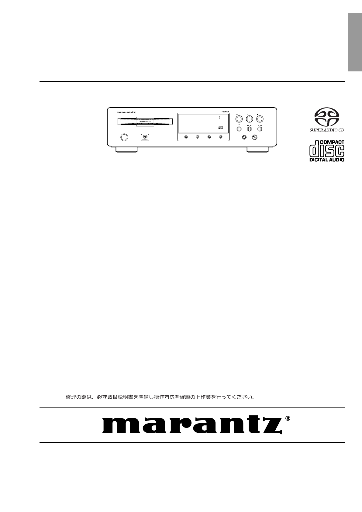
Super Audio CD Player
SUPER AUDIO CD PLAYER SA8400
DISPLAY
OFF
POWER
ON/OFF
SOUND MODE
TIME
DISPLAY
TEXT
TABLE OF CONTENTS
OPEN/CLOSE
PLAY
PAUSE
STOP
/
/
LEVEL
PHONES
+
-
MECHA LOADER AND MECHA TRAVERSE
2.1 EXPLODED VIEW AND PARTS LIST........................................................................................ 2-1
SUPER AUDIO CD PCB MODULE
3.1 IC DATA...................................................................................................................................... 3-1
3.2 BLOCK DIAGRAM ................................................................................................................... 3-22
3.3 SCHEMATIC DIAGRAM........................................................................................................... 3-34
3.4 PARTS LOCATION................................................................................................................... 3-36
3.5 ELECTRICAL PARTS LIST...................................................................................................... 3-38
Please use this service manual with referring to the user guide ( D.F.U. ) without fail.
SA8400
Part no. 13AK855012
2nd Issue 2003.12
ecm
Page 2
MARANTZ DESIGN AND SERVICE
Using superior design and selected high grade components,
Only original
MARANTZ
parts can insure that your
MARANTZ
MARANTZ
product will continue to perform to the specifi cations for which
company has created the ultimate in stereo sound.
it is famous.
Parts for your
MARANTZ
ORDERING PARTS :
equipment are generally available to our National Marantz Subsidiary or Agent.
Parts can be ordered either by mail or by Fax.. In both cases, the correct part number has to be specifi ed.
The following information must be supplied to eliminate delays in processing your order :
1. Complete address
2. Complete part numbers and quantities required
3. Description of parts
4. Model number for which part is required
5. Way of shipment
6. Signature : any order form or Fax. must be signed, otherwise such part order will be considered as null and void.
USA
MARANTZ AMERICA, INC
1100 MAPLEWOOD DRIVE
ITASCA, IL. 60143
USA
PHONE : 630 - 741 - 0300
FAX : 630 - 741 - 0301
AMERICAS
SUPERSCOPE TECHNOLOGIES, INC.
MARANTZ PROFESSIONAL PRODUCTS
2640 WHITE OAK CIRCLE, SUITE A
AURORA, ILLINOIS 60504 USA
PHONE : 630 - 820 - 4800
FAX : 630 - 820 - 8103
EUROPE / TRADING
MARANTZ EUROPE B.V.
P. O. BOX 8744, BUILDING SILVERPOINT
BEEMDSTRAAT 11, 5653 MA EINDHOVEN
THE NETHERLANDS
PHONE : +31 - 40 - 2507844
FAX : +31 - 40 - 2507860
AUSTRALIA
TECHNICAL AUDIO GROUP PTY, LTD
43-53 Bridge Rd.,
STANMORE NSW 2048
AUSTRALIA
PHONE : +61 - (0)2 - 9519 - 0900
FAX : +61 - (0)2 - 9519 - 0600
CANADA
LENBROOK INDUSTRIES LIMITED
633 GRANITE COURT,
PICKERING, ONTARIO L1W 3K1
CANADA
PHONE : 905 - 831 - 6333
FAX : 905 - 831 - 6936
HONG KONG
Jolly ProAudio Broadcast Engineering Ltd.
UNIT 2, 10F, WAH HUNG CENTRE,
41 HUNG TO ROAD, KWUN TONG, KLN.,
HONG KONG
PHONE : 852 - 21913660
FAX : 852 - 21913990
AUSTRALIA
QualiFi Pty Ltd,
24 LIONEL ROAD,
MT. WAVERLEY VIC 3149
AUSTRALIA
PHONE : +61 - (0)3 - 9543 - 1522
FAX : +61 - (0)3 - 9543 - 3677
NEW ZEALAND
WILDASH AUDIO SYSTEMS NZ
14 MALVERN ROAD MT ALBERT
AUCKLAND NEW ZEALAND
PHONE : +64 - 9 - 8451958
FAX : +64 - 9 - 8463554
JAPAN
MARANTZ JAPAN, INC.
35- 1, 7- CHOME, SAGAMIONO
SAGAMIHARA - SHI, KANAGAWA
JAPAN 228-8505
PHONE : +81 42 748 1013
FAX : +81 42 741 9190
Technical
THAILAND
MRZ STANDARD CO., LTD
746 - 754 MAHACHAI ROAD.,
WANGBURAPAPIROM, PHRANAKORN,
BANGKOK, 10200 THAILAND
PHONE : +66 - 2 - 222 9181
FAX : +66 - 2 - 224 6795
TAIWAN
PAI- YUING CO., LTD.
6 TH FL NO, 148 SUNG KIANG ROAD,
TAIPEI, 10429, TAIWAN R.O.C.
PHONE : +886 - 2 - 25221304
FAX : +886 - 2 - 25630415
SHOCK, FIRE HAZARD SERVICE TEST :
SINGAPORE
WO KEE HONG DISTRIBUTION PTE LTD
130 JOO SENG ROAD
#03-02 OLIVINE BUILDING
SINGAPORE 368357
PHONE : +65 6858 5535 / +65 6381 8621
FAX : +65 6858 6078
MALAYSIA
WO KEE HONG ELECTRONICS SDN. BHD.
2ND FLOOR BANGUNAN INFINITE CENTRE
LOT 1, JALAN 13/6, 46200 PETALING JAYA
SELANGOR DARUL EHSAN, MALAYSIA
PHONE : +60 - 3 - 7954 8088
FAX : +60 - 3 - 7954 7088
KOREA
MK ENTERPRISES LTD.
ROOM 604/605, ELECTRO-OFFICETEL, 16-58,
3GA, HANGANG-RO, YONGSAN-KU, SEOUL
KOREA
PHONE : +822 - 3232 - 155
FAX : +822 - 3232 - 154
CAUTION : After servicing this appliance and prior to returning to customer, measure the resistance between either primary AC
cord connector pins ( with unit NOT connected to AC mains and its Power switch ON ), and the face or Front Panel of product
and controls and chassis bottom.
Any resistance measurement less than 1 Megohms should cause unit to be repaired or corrected before AC power is applied,
and verifi ed before it is return to the user/customer.
Ref. UL Standard No. 1492.
In case of diffi culties, do not hesitate to contact the Technical
Department at above mentioned address.
030307MIT
Page 3

1. TECHNICAL SPECIFICATIONS AND UPDATE DISC
Super Audio CD CD
Audio Characteristics
Analog output
Channels 2channels 2channels
Frequency range 2Hz — 100kHz 2Hz — 20kHz
Frequency characteristics 2Hz — 50kHz (-3dB) 2Hz — 20kHz
Dynamic range 114dB More than 100dB
THD (1kHz) 0.0009% 0.0020%
Wow & Flutter Precision of quartz Precision of quartz
Output level 2.2V 2.2V
Digital output
Output level (Cinch JACK) — 0.5Vp-p (75Ω)
Output level (Optical) — -19dBm
Headphone output level 0.5W / 32Ω (max, Vol.) 0.5W / 32Ω (max, Vol.)
Optical Readout System
Laser AlGaAs AlGaAs
Wave length 650nm 780nm
Signal format 1-bit DSD 16-bit linear PCM
Sampling frequency 2.8224MHz 44.1kHz
Power Supply
Input Voltage, Frequency (/F).................................................................... AC 100V 50/60Hz
(/K/L)............................................................. AC 110/220V 50/60Hz
(/N)......................................................................... AC 230V 50Hz
(/S)......................................................................... AC 230V 50Hz
Power Consumption....................................................................................................... 20W
Cabinet, etc.
Dimensions ...............................................................................................
Net weight.....................................................................................................................7.5kg
Operating temperatures.................................................................................. +5°C ~ +35°C
Operating humidity............................................................................. 5 ~ 90% (without dew)
Accessories
• Remote control unit (RC8400SA) ......................................................................................1
Dimensions (Width × Height × Depth)..............................................
Net weight (without Batteries) .......................................................................................60g
• AAA (R03) Batteries ..........................................................................................................2
• AC Power cord...................................................................................................................1
• Audio cable...............................................................................................................1 pairs
• Remote connection Cable ................................................................................................1
• User’s Guide......................................................................................................................1
440 × 113 × 335mm
48.5 × 21.5 × 152.5mm
UPDATE DISC
Update of the CPU (IC731)..............................................................................*SA8400CDR
1
Page 4
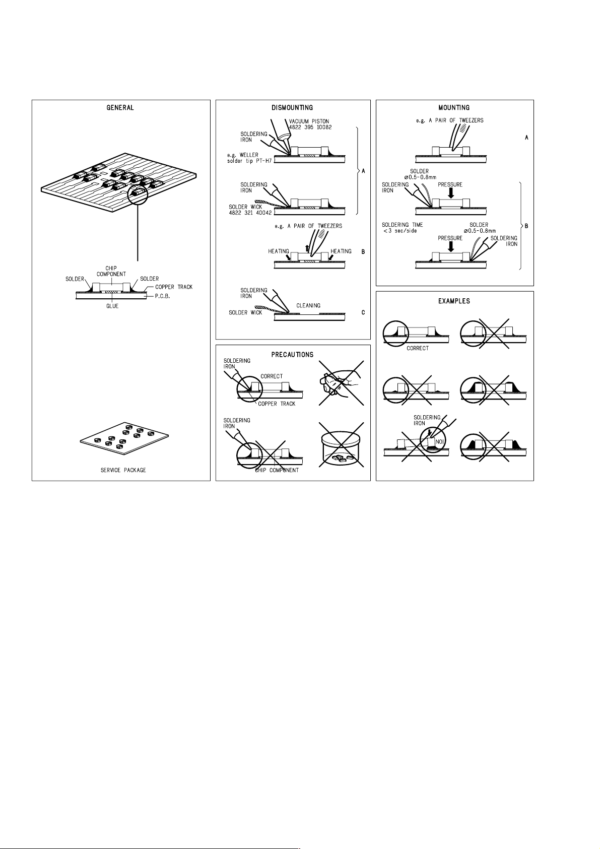
2. SERVICE HINTS AND TOOLS
SERVICE HINTS
SERVICE TOOLS
Audio signals disc 4822 397 30184
Disc without errors (SBC444)+
Disc with DO errors, black spots and fingerprints (SBC444A) 4822 397 30245
Disc (65 min 1kHz) without no pause 4822 397 30155
Max. diameter disc (58.0 mm) 4822 397 60141
Torx screwdrivers
Set (straight) 4822 395 50145
Set (square) 4822 395 50132
13th order filter 4822 395 30204
DVD test disc (PAL) 4822 397 10131
DVD test disc (NTSC) ALMEDIO TDV-540
2
Page 5
3. WARNING AND LASER SAFETY INSTRUCTIONS
GB
WARNING
All ICs and many other semi-conductors are
susceptible to electrostatic discharges (ESD).
Careless handling during repair can reduce
life drastically.
When repairing, make sure that you are
connected with the same potential as the
mass of the set via a wrist wrap with
resistance.
Keep components and tools also at this
potential.
F
ATTENTION
D
WARNUNG
I
WAARSCHUWING
AVVERTIMENTO
NL
Alle IC’s en vele andere halfgeleiders zijn
gevoelig voor elektrostatische ontladingen
(ESD).
Onzorgvuldig behandelen tijdens reparatie
kan de levensduur drastisch doen
verminderen.
Zorg ervoor dat u tijdens reparatie via een
polsband met weerstand verbonden bent met
hetzelfde potentiaal als de massa van het
apparaat.
Houd componenten en hulpmiddelen ook op
ditzelfde potentiaal.
Tous les IC et beaucoup d’autres semiconducteurs sont sensibles aux décharges
statiques (ESD).
Leur longévité pourrait être considérablement
écourtée par le fait qu’aucune précaution
n’est prise a leur manipulation.
Lors de réparations, s’assurer de bien être
relié au même potentiel que la masse de
l’appareil et enfiler le bracelet serti d’une
résistance de sécurité.
Veiller a ce que les composants ainsi que les
outils que l’on utilise soient également a ce
potentiel.
GB
Safety regulations require that the set be restored to its original condition
and that parts which are identical with those specified be used.
NL
Veiligheidsbepalingen vereisen, dat het apparaat in zijn oorspronkelijke
toestand wordt terug gebracht en dat onderdelen, identiek aan de
gespecifieerde worden toegepast.
Alle IC und viele andere Halbleiter sind
empfindlich gegen elektrostatische
Entladungen (ESD).
Unsorgfältige Behandlung bei der Reparatur
kann die Lebensdauer drastisch vermindern.
Sorgen sie dafür, das Sie im Reparaturfall
über ein Pulsarmband mit Widerstand mit
dem Massepotential des Gerätes verbunden
sind.
Halten Sie Bauteile und Hilfsmittel ebenfalls
auf diesem Potential.
D
Bei jeder Reparatur sind die geltenden Sicherheitsvorschriften zu beachten.
Der Originalzustand des Gerats darf nicht verandert werden.
Fur Reparaturen sind Original-Ersatzteile zu verwenden.
I
Le norme di sicurezza esigono che l’apparecchio venga rimesso nelle
condizioni originali e che siano utilizzati pezzi di ricambiago idetici a quelli
specificati.
Tutti IC e parecchi semi-conduttori sono
sensibili alle scariche statiche (ESD).
La loro longevita potrebbe essere fortemente
ridatta in caso di non osservazione della piu
grande cauzione alla loro manipolazione.
Durante le riparazioni occorre quindi essere
collegato allo stesso potenziale che quello
della massa dell’apparecchio tramite un
braccialetto a resistenza.
Assicurarsi che i componenti e anche gli
utensili con quali si lavora siano anche a
questo potenziale.
F
“Pour votre sécurité, ces documents
doivent être utilisés par des
spécialistes agrées, seuls habilités à
réparer votre appareil en panne.”
Les normes de sécurité exigent que l’appareil soit remis a l’état d’origine et
que soient utilisées les pièces de rechange identiques à celles spécifiées.
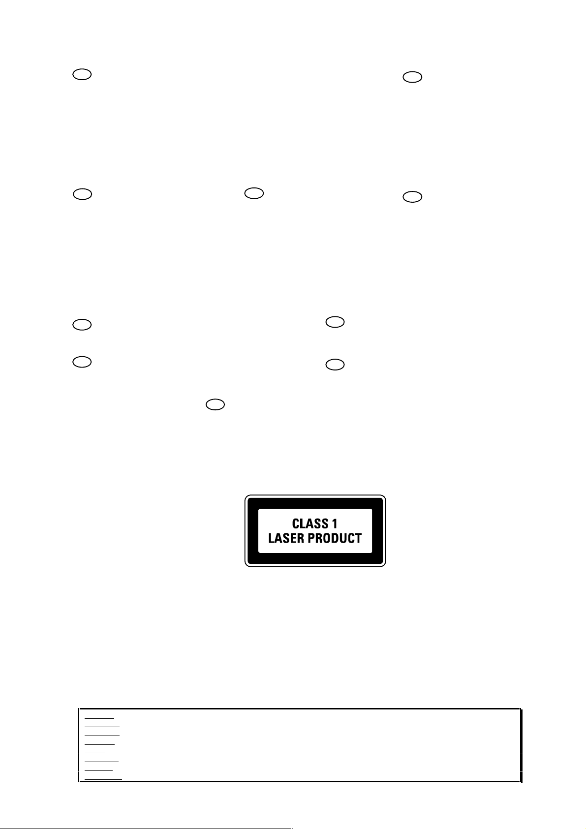
LASER SAFETY
This unit employs a laser. Only a qualified service person should remove the cover or attempt to service this
device, due to possible eye injury.
USE OF CONTROLS OR ADJUSTMENTS OR PERFORMANCE OF PROCEDURE OTHER THAN THOSE
SPECIFIED HEREIN MAY RESULT IN HAZARDOUS RADIATION EXPOSURE.
AVOID DIRECT EXPOSURE TO BEAM
WARNING
The use of optical instruments with this product will increase eye hazard.
Repair handling should take place as much as possible with a disc loaded inside the player
WARNING LOCATION: INSIDE ON LASER COVERSHIELD
CAUTION VISIBLE AND INVISIBLE LASER RADIATION WHEN OPEN AVOID EXPOSURE TO BEAM
ADVARSEL SYNLIG OG USYNLIG LASERSTRÅLING VED ÅBNING UNDGÅ UDS
ADVARSEL SYNLIG OG USYNLIG LASERSTRÅLING NÅR DEKSEL Å PNES UNNGÅ EKSPONERING FOR STRÅLEN
VARNING SYNLIG OCH OSYNLIG LASERSTRÅLNING NÄR DENNA DEL ÄR ÖPPNAD BETRAKTA EJ STRÅLEN
VARO! AVATT AESSA OLET ALTTIINA NÄKYVÄLLE JA NÄKYMÄTTÖMÄLLE LASER SÄTEILYLLE. ÄLÄ KATSO SÄTEESEEN
VORSICHT SICHTBARE UND UNSICHTBARE LASERSTRAHLUNG WENN ABDECKUNG GEÖFFNET NICHT DEM STRAHL AUSSETSEN
DANGER VISIBLE AND INVISIBLE LASER RADIATION WHEN OPEN AVOID DIRECT EXPOSURE TO BEAM
ATTENTION RAYONNEMENT LASER VISIBLE ET INVISIBLE EN CAS D'OUVERTURE EXPOSITION DANGEREUSE AU FAISCEAU
Æ
TTELSE FOR STRÅLING
030804ecm
3
Page 6

4. TAKING THE DISC OUT OF EMERGENCY
1. To open the stucked tray, insert a pin into the eject pinhole and push the eject lever.
2. Use a pin φ4mm or less.
This picture shows the unit upside down. The eject lever is pointed by the arrow.
The lever is thin so aim the narrow area carefully.
4
Page 7
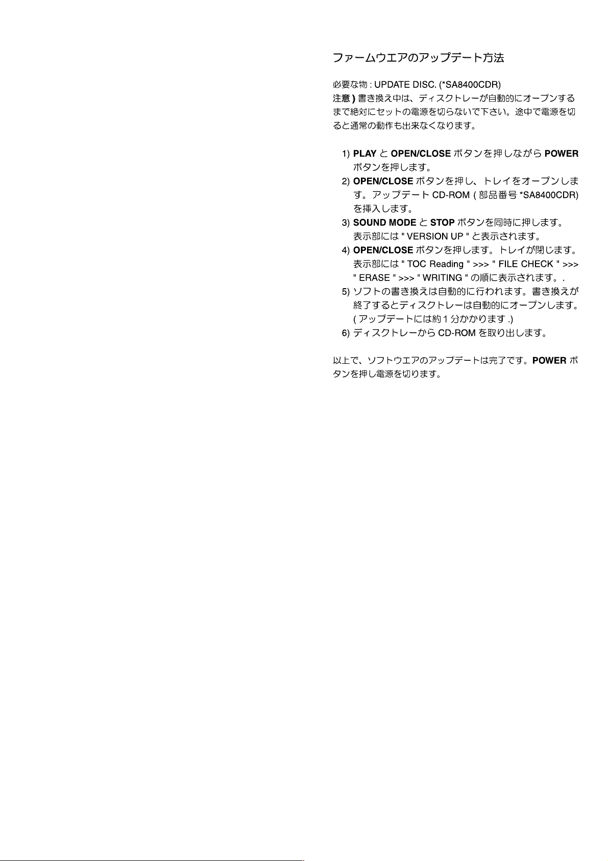
5. UPDATE FIRMWARE
Have UPDATE DISC. (*SA8400CDR)
Attention : Don't turn off the unit until disk tray opens
automatically during the updating. When the turn off the unit
halfway, The unit can't be operated any more.
1) Press the POWER button while pressing the PLAY and
OPEN/CLOSE buttons.
2) Press the OPEN/CLOSE button to open the tray, Insert
the update CD-ROM (part No.:*SA8400CDR).
3) Press the SOUND MODE and STOP buttons.
The Display indicates " VERSION UP ".
4) Press the OPEN/CLOSE button to close the tray.
The Display indicates " TOC Reading " >>> " FILE
CHECK " >>> " ERASE " >>> " WRITING ".
5) Software updating will be done automatically.
When the updating is fi nished, The disc tray opens
automatically.
(Updating takes about 1 minute.)
6) Remove the CD-ROM from the disc tray.
Update is completed, Press the POWER button to turn off the
unit.
5
Page 8
6. SERVICE MODE
The error code is indicated when a problem DISC is inserted fi rst.
Press the POWER button While pressing PLAY and OPEN/CLOSE Button
Press<
Press<
Press<
"SA8400" is displayed
>
Version of Backend(IC731) µ-COM is displayed
"B/E VXX.XX" is displayed
>
"DRV VXX.XX" is displayed
>
All area in the FLD light on
Press< >
All area in the FLD light off
Press< >
Press<
"H.R.SHORT" is displayed Appear Errer Code
"H.R.CHACKING" is displayed
> or Press PLAY< >
(Ex:E1 0000)
Press<
>
"H.R.NORMAL" is displayed
Remove Mains cord from plug
Errer Code
Error Code Error
E1 XXXX Operation time Error
E2 XXXX T.O.C Error
E2 XXXX Focus Error
E2 XXXX Read Error
E4 XXXX Tracking Error
E5 XXXX Tray Error
E6 XXXX Navigation Pack Read Error
E7 XXXX Check Sum Eroor and
NonAcknow I edgmen
NO DISC XXXX NO disc
(XXXX: The Operation number of times to the error
occurrence)
6
Page 9
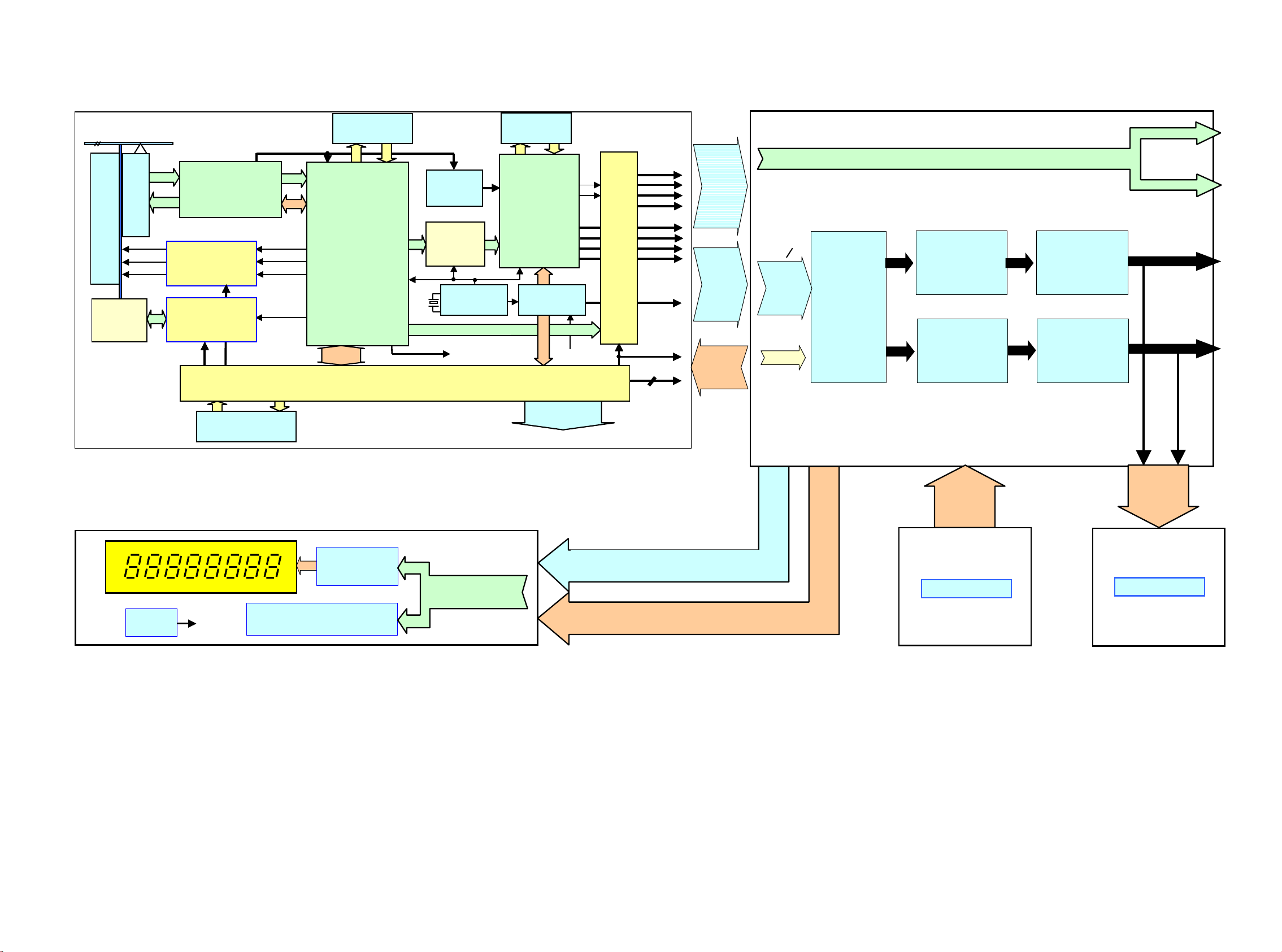
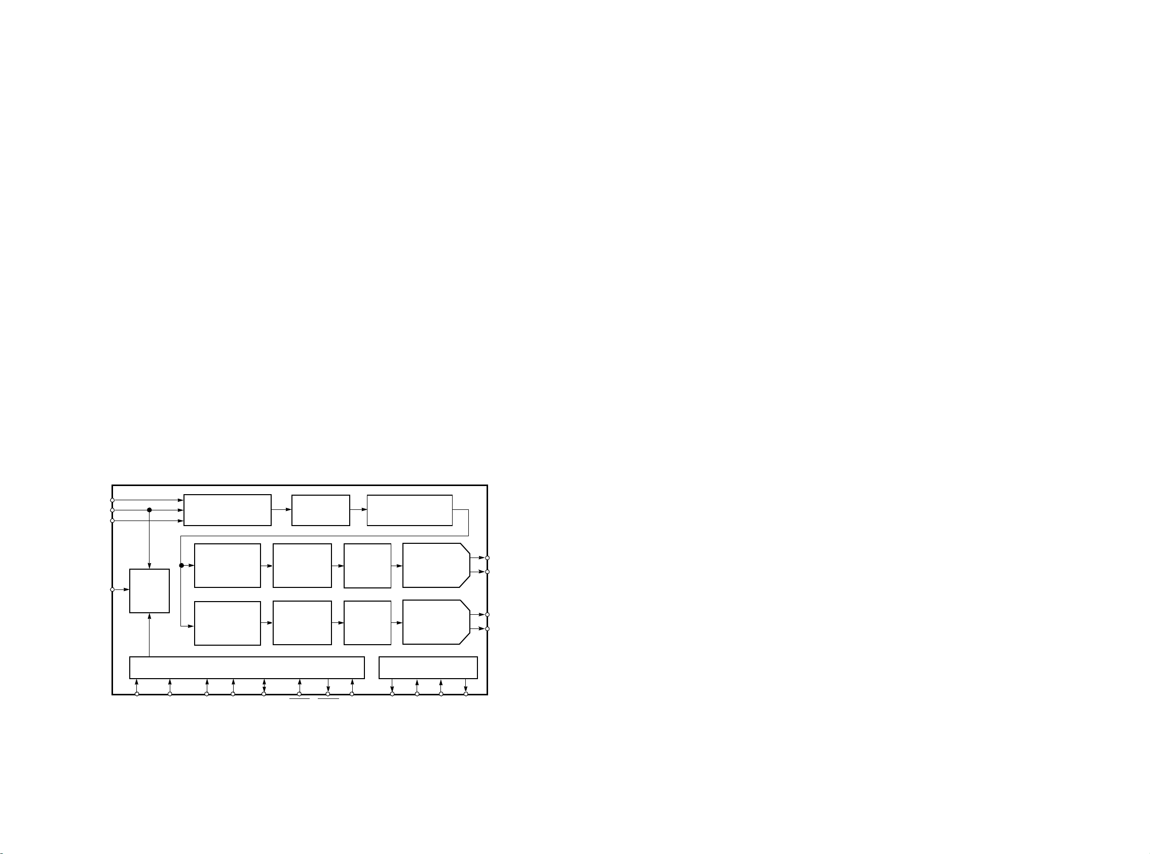
7. BLOCK DIAGRAM
SERVO BLOCK MAIN BLOCK
TURNTABLE
FOC,RAD,SLDG
3-AXICAL ACTUATOR
SPINDL
HOLL
MOTOR
photo
Laser
control
CD and DVD
LASER and MONITOR
LASER POWER CONT.
FAN8042
FOC,RAD,SLED
AN8471SA
SPINDLE DRIVER
CXD1881AR
IC501
RF-AMP, AGC, EQ
IC508
DRIVER
IC505
T14L1024N
IC732
SRAM(1M)
FOC
RAD
SLED
SPIN
M11L16161SA-45T
IC503
RFAC
D-RAM(16M)
AD6062
IC403
RF-AMP
CXD1885Q
IC502
DIGITAL SERVO
and PLL,
DEMODURATOR
EPM33128
IC404
FIFO
SYSTEM CLOCK
33.8688MHz
PCM DATA BUS LINE
M30624FGN
FEATUR and LOADING for SERVO-DSP
IC731
OSC IC734
DIGITAL I/O
EM636165TS-7
IC402
SDRAM(16M)
CXD2753R
IC401
PSP DECORD
and
DSD MULTI-
CHANNL
DECODER
CLK SELECTOR
IC735
384/192fs
DISPLAY and KEYS
DATA
SYCLSW
LRCK
DAPC
DARD
DACL
DSALF
DSAC
DSALS
DSARS
IC736
DSD/CD
DATA SWITCH
SYCL
DSCK
DSDO
DSCS1
DSRT1
ATT
MUTE1
384/192fs
MODE
and
DAC CONTROL
PCM/DSD DATA
KEYS DATA
DISPLAY and
POWER
SUPPLY
DIG. OUT PART
DIGITAL I/O
DAC PART
DAPC/DARD
DACL/LRCK
SYCL
CONTROL
CS4397
WOOFER/
CENTER
2CH DAC
HDAM
Diffrencial AMP
&
2th-LPF
HDAM
Diffrencial AMP
&
2th-LPF
HDAM
Current
Feedback AMP
&
2th-LPF
HDAM
Current
Feedback AMP
&
2th-LPF
COAX
OPT
L ch
R ch
POWER HEADPHONE
SUPPLY BLOCK
FRONT UNIT BLOCK BLOCK
IR sensor
RC-5
ML9207-01GP
FTD DRIVER
KEYS
PLAY/STOP/PAUSE/NEXT/PREVI/etc
DISPLAY and KEYS /RC-5 DATA
POWER SUPPLY
POWER
SUPPLLY
TRANSFORMER
HEADPHONE
L/R
HEADPHONE
7 8
Page 10
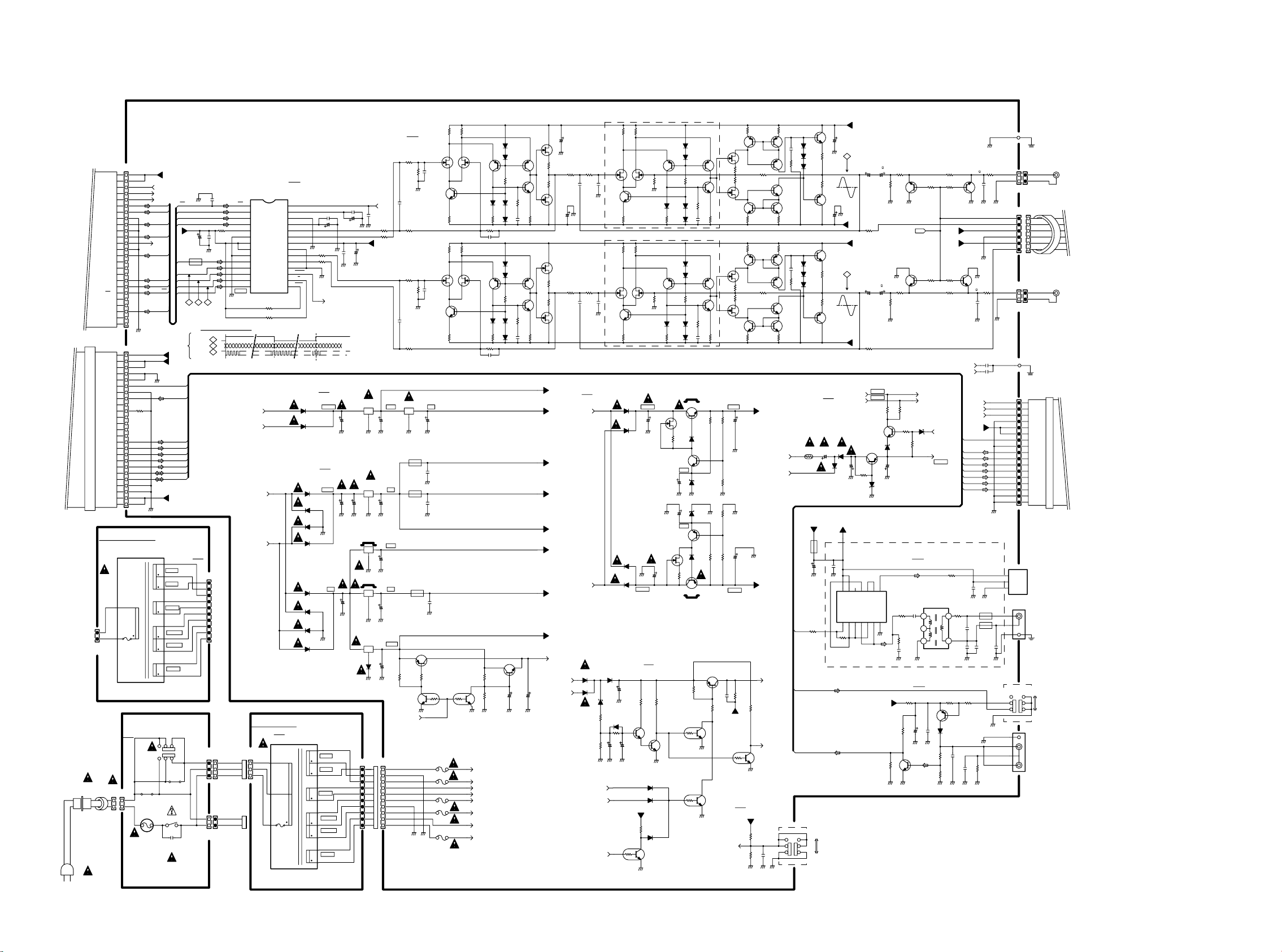
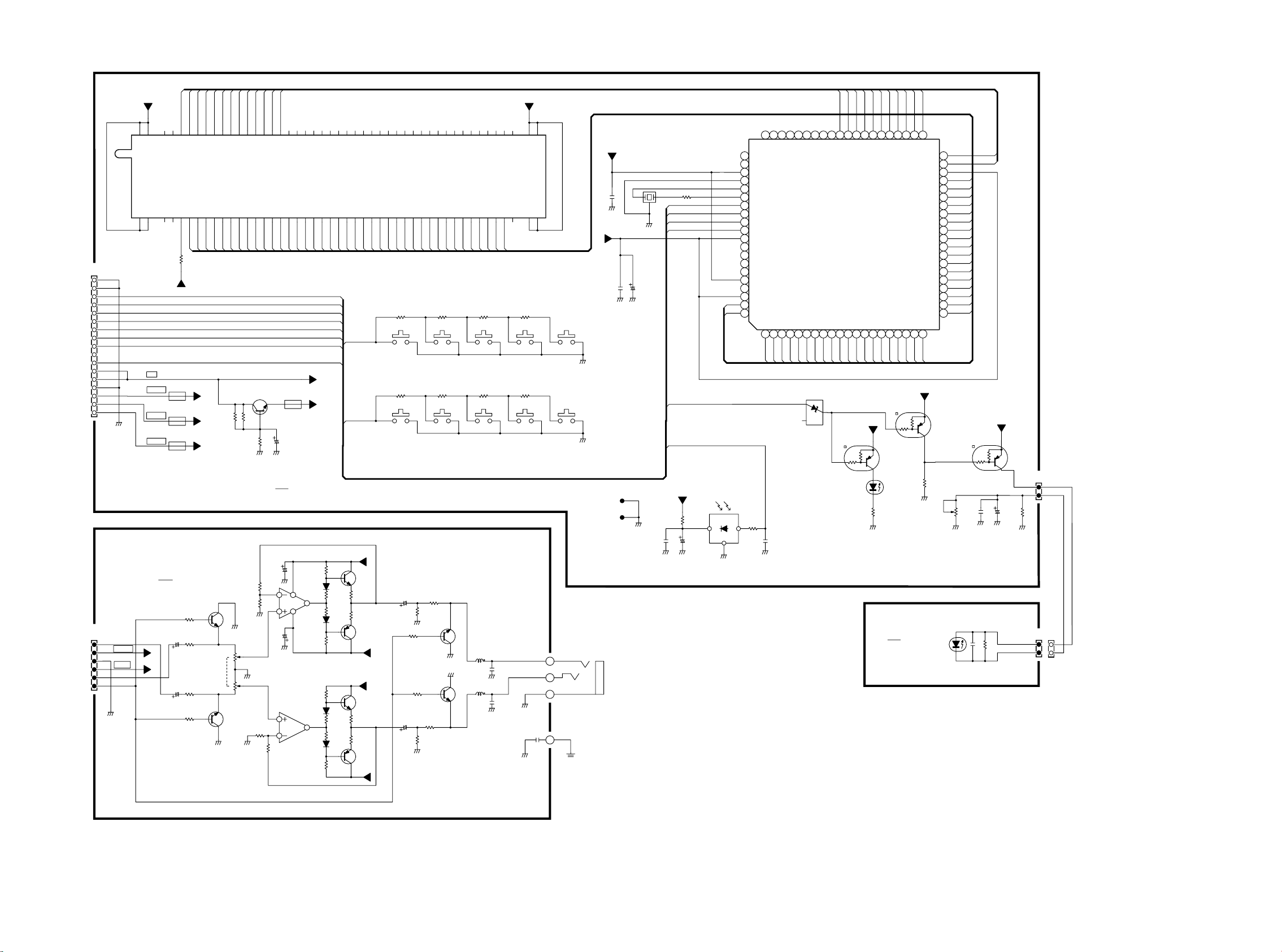
8. SCHEMATIC DIAGRAM
WF05
+5B
+5B
LPFSW
MODE1
MUT1
DAPC
DARD
GND
SYCL
GND
DACL
M0/ATT
GND
M41
M42
DSALS
TO SERVO PCB(PV16)
DSARS
DSD DATA IN AND POWER OUT
M3
M2
RST
M43
MUT2
DALR
DSALF
DSAC
WF04
+12M
P8M
P8M
MGN
MGN
DIGO
GND
RC5S
USER2
USER1
CDLED
SALED
MLTLED
LEY2
DISPLED
L012
HF70SH28X2X10
FRES
FCEN
FCLK
FDAT
KEY1
KEY0
GND
GND
+5A
+5A
TO SERVO PCB(PV16)
DSD DATA IN AND POWER OUT
FOR F,N,S
(PH26) TRANSF.PCB
L001
2
1
JH04
for F,S,N,U
J001
W003
HF-301
(F,N,S only)
(F,N,S only)
2
1
L003
TFCK-23-11-14
W001
(F,N,S only)
W002(K,L only)
(PP16)
MAIN PCB
JF02
25FMN-BTRK
1
2
3
4
5
6
7
8
9
10
11
12
13
14
15
16
17
18
19
20
21
22
23
24
25
10
11
12
13
14
15
16
17
18
19
20
21
22
23
24
25
4
2
JF01
25FMN-BTRK
1
2
3
4
5
6
7
8
9
LPFSW
MODE1
MUT1
ATT
GND
M-GND
RY51
100
GND
(PH16)
POWER SW PCB
LPT
SH02
for K,L
12
JH01
UH04
2
for F,S,N,U
1
FH01
L 250V
T1.25A
JUMPER (F only)
POWER & DAC
+5B
RST
DAPC
M41
DARD
M3
M2
SYCL
3VDA
DACL
M41
SYCL
DACL
DALR
M3
DAPC
M2
DARD
RST
14
DALR
+12M
P8M+5A
DIGO
RC5S
DISPLED
FRES
FCEN
FCLK
FDAT
KEY1
KEY0
11
AC13V
12
AC13V
13
14
AC4.3V
15
16
AC11.8V
17
AC11.8V
18
19
AC7.3V
20
321
654
12
UH05
NC
SH01
21
GH01
0.01
AC250V
GND
0.1
CD61
100 25V
CD62
GND
LD01
384/192fs
12
15
16
DAC DATA INPUT FIG
15
DACK
DAD1,3,5
16
SCLK
14
LPT
WH02
10
9
8
7
6
5
4
3
2
1
JH03
for K,L
3
2
1
2
1
JH02
for F,S,N.U
QD61
1000p
CD70
RD63
10k
GND
M
CS4397
128
RST VREF
2
M4/ADD
3
M3/AD1
4
M2/SC1
5
M0/SDA
6
DGND
7
VD
8
VD
9
DGND
10
MCLK
11
SCLK
12
CMOD
13
SDAT
14
M1
CD=H
RD64
18k
RD65
18k
L,CH
L
3AC11
5AC11
1AC8
2AC8
FOR K,L
L001
JH05
for K,L
WH03
3
2
1
for F,S,N.U
2
1
for K,L
WH01
5
3
220V
3
2
110V
2
1
1
0V
4
2
1
2
LDA
27
FILT+
26
FILT-
25
CMOUT
24
-LO
23
+LO
22
VA
21
GND
20
+RD
19
-RD
18
GND
17
MUTEC
16
C/H
15
MUTE
R,CH
M
LPT
CD68
0.1
CD66
CD67
100 10V
10 25V
CD65
GND
GND
1.2k
R652
R651
L
CD63
1.2k
GND
GND
MUTEC
M
LPS
D822
+15.1V
1D3
D821
1D3
M-GND
C821
4700 25V
LPS
D803
11EQS10
+7.9V
D802
11EQS10
D804
11EQS10
D801
11EQS10
D807
11EQS10
D806
11EQS10
D808
11EQS10
D805
11EQS10
GND
GND
GND GND
+8V
GND
C801
6800 16V
C805
NJM78M05F
(PH26)
TRANSF.PCB
11
AC13V
12
AC13V
13
14
AC4.3V
15
16
AC11.8V
17
AC11.8V
18
19
AC7.3V
20
6800 16V
0.1
GND
GND
BA033T
Q803
LFB
R603
560
R604
QD01
Q802
0.1
IN
BA05T
10
C804
9
8
7
6
5
4
3
2
1
VREF
GND
CD64
100 25V
Q821
NJM7812F
COM
3300 16V
035G
TR SHILED
035G
TR SHILED
WH02
GND
2
M-GND
2
2
GND
2
GND
2
GND
Q801
BA05T
5V
0.1
CD69
13
OUT
13
COM
13
COM
13
COM
13
COM
D809
DTGDTG
C601
VREF
1800p
R605
R601
3.9k
1.2k
R602
1.2k
5.6VA
R653
560
R654
C651
1800p
R655
3.9k
Q822
NJM7808F
+12V
2
COM
C822
2200 16V
M-GND M-GND
M-GND
L802
12
L803
+5V
OUTIN
12
C802
3300 6.3V
GND
3.3V TO DAC
OUTIN
CD26
220 25V
GND
L801
+5V
OUTIN
OUTIN
11EQS10
12
C806
3300 6.3V
GND
+5.6V
C809
1000 10V
4.7k
RD22
GND
MODE1
J801
10
9
8
7
6
5
4
3
2
1
M-GND
120
R606
R607
Q601
2SK369 BL
D
D
3
3
+
1
G
2
2
S
S
330p
C602
1.8k
GND
2SC2240
C652
1.8k
330p
GND
2SC2240
+8V
OUTIN
13
C823
C807
GND
C808
GND
GND
123
E
C
QD23
2SA970
B
Y,GR
1.2k
RD23
1
3
QD21
DTC114TS
GND GND GND GND GND
T800mA L 250V
T800mA L 250V
T1A L 250V
GND
T1.25A L 250V
Q603
GR,BL
Q651
2SK369 BL
+
DTG DTG
Q653
GR,BL
2200 16V
0.10.1
0.1
C803
F852
F851
F822
F821
T1A
L 250V
F801
2SK369 BL
C
1
2
B
E
3
68
R608
120
R657
R656
D
D
3
3
1
G
2
2
S
S
2SK369 BL
C
1
2
B
E
3
68
R658
2
2
QD22
DTC114TS
10AC12
8AC12
H1
H2
5AC11
3AC11
2AC8
1AC8
DIFFERENCIAL
120
Q604
2SA970
3
E
GR,BL
-
1
2
G
B
1
C
Q602
D601
D604
560
D605
R609
5.1k
R615
C604
DAMG
120p
120
Q654
2SA970
3
E
GR,BL
-
1
2
G
B
1
C
Q652
D651
D654
560
R659
D655
5.1k
R665
120p
C654
DAMG
123
1.5k3.9k
RD24RD25
1
3
10AC12
8AC12
H1
H2
5AC11
3AC11
2AC8
1AC8
C
D602
Q605
2SA970
GR,BL
D603
2
B
Q606
2SC2240
GR,BL
33k
R610
2
B
R611
100
47p
C603
D652
Q655
2SA970
GR,BL
D653
2
B
Q656
2SC2240
GR,BL
33k
R660
2
B
100
R661
47p
C653
TO SERVO
TO SERVO
TO DIG. OUT
TO DAC(5.5/3.5V)
E
QD24
B
2SC2878
CD21
10 63V
Q607
2SK170
3
D
C605
V
220 16V
1
G
GND 2SA970
2
S
E
3
33
R622
R613
2SJ74
2SK170
2SJ74
CD22
2.2k
S
2
G
1
ARA
Q608
D
3
V
GND
C606
220 16V
Q657
D
3
V
1
G
S
2
33 33
R672
R663 R614
2.2k
33
R664
S
2
G
1
D
Q658
3
V
+12M
P8M
+5B
+5F
+5VD
3VDA
+5A
5.6VA
VREF
5AC11
3AC11
100 10V
C
C
E
560
R612
E
C
C
E
560
R662
TO SERVO
TO FRONT
TO SERVO
TO DAC
1
1
3
3
1
1
3
()
ARA
DTG
C609
1200p
DTG
C659
1200p
H:MUTE ON
L:MUTE OFF
H:MUTE ON
L:MUTE OFF
H:MUTE OFF
L:MUTE ON
LPS
8AC12
10AC12
DN02
ID3
DN01
ID3
R623
3.3k
R673
3.3k
560p
C610
GND
560p
C660
GND
RN01
M-GND M-GND
)(
)(
031G HDAM SHILED (S,K only)
120
120
R625
R624
Q609
2SK369 BL
D
D
3
3
+
1
1
G
G
2
2
S
S
GR,BL
Q610
2SK369 BL
1
C
Q611
2
B
3
E
68
R626
DTGDTG
2SC2240
031G HDAM SHILED (S,K only)
120
120
R675
R674
Q659
2SK369 BL
D
D
3
3
+
Q661
2SC2240
GR,BL
1
1
G
G
2
2
S
S
Q660
C
1
2SK369 BL
2
B
E
3
68
R676
D854
11EQS10
+12.6V
D853
11EQS10
GND
D852
11EQS10
D851
GND
11EQS10
-12.6V
LMU
DN05
ID3
CN01
1000 25V
M-GND
DN06
4.7V
RN09
47k
RN06
1.2k
QN06
DN07
2SC2458
C
1
Y,GR
2
B
RN10
2.2M
3
15k
ATT
MUT1
MUTEC
E
CN03
CN02
4.7 50V
QN01
1 100V
2SC2458
Y,GR
M-GND
3VDA
RN65
QN65
N.C.
1
2
3
GND
Q612
E
3
GR,BL
1
-
C
270
R627
GND
D606
560
R628
Q662
2SA970
E
3
GR,BL
1
-
C
270
R677
GND
D656
560
R678
S
G
C851
3300 25V
1
D
2SC2240
Q855
2SK246
GR
G
1
C852
3300 25V
RN02
10k
H:MUTE ON
L:MUTE OFF
C
1
2
B
E
3
M-GND
DN12
DN11
N.C.
N.C.
DN61
2
2
2
3
GR,BL
C856
R852
D607
D608
B
33k
R629
D609
D610
D657
D658
B
33k
R679
D659
D660
035G
TR SHILED
Q852
231
CBE
Q851
2SK246
GR
100
R851
Q853
6.2V
ARA
C855
10 25V
ARA
10 25V
6.2V
GR,BL
Q857
2SA970
S
2
D
3
100
C
231
Q856
DTC114TS
)(
2
DTC114TS
2
CURRENT LPF
Q613
2SA970
E
3
GR,BL
2
B
1
C
Q614
C
1
2SC2240
GR,BL
2
B
E
3
47
R630
33p
560
C611
R631
Q663
2SA970
E
3
GR,BL
2
B
1
C
Q664
C
1
2SC2240
GR,BL
2
B
E
3
47
R680
33p
560
C661
R681
2SD1415A
R858
D858
1
C
2
B
3
E
D856
HZ6L-3
GNDGND GND
GNDGND GND
D857
HZ6L-3
3
E
2
B
1
C
D859
3.3k
R857
B
E
2SB1020A
035G
TR SHILED
QN04
2SA1048
Y.GR
E
B
RN03
47k
RN04
47k
QN02
1
3
M-GND
QN66
1
3
M-GND
Q623
Q618
270270
R634
E
3
Q617
2SA970
GR,BL
Q615
1
C
2SK170
D
3
V
1
G
2
S
100
R632
Q616
100
R633
2SJ74
S
2
V
G
1
3
D
C
1
Q620
2SC2240
GR,BL
3
E
R636
270
R684
E
3
Q667
2SA970
GR,BL
Q665
1
C
2SK170
D
3
V
1
G
2
S
100
R682
Q666
100
R683
2SJ74
S
2
V
G
1
3
D
C
1
Q670
2SC2240
GR,BL
3
E
270
R686
TO AUDIO
11.4V
R853
C857
3.3k
2.7k
470 16V
GND
3.3k2.7k
R854R855
3.3k
R856
2
B
2
B
2
B
2
B
2SA970
GR,BL
2SA970
GR,BL
270
R635
2SA970
E
3
GR,BL
2
B
1
C
Q619
E
3
2
B
R641
1
120
C
C
1
2
2SC2240
B
GR,BL
3
E
C
1
2
2SC2240
B
GR,BL
3
E
270
R637
Q668
270
R685
2SA970
E
3
GR,BL
2
B
1
C
Q669
3
E
2
B
R691
1
120
C
C
1
2
2SC2240
B
GR,BL
3
E
C
1
2
2SC2240
B
GR,BL
3
E
270
R687
+12V
5AC11
3AC11
C
2SC2240
GR,BL
2
B
DTG
E
D611
680p
C612
D612
47
R638
D613
Q622
Q624
2SA970
E
GR,BL
2
B
Q621
C
Q673
C
2SC2240
GR,BL
2
B
DTG
E
D661
C662
680p
D662
47
R688
D663
Q672
Q674
2SA970
E
GR,BL
2
B
Q671
C
CY51
RY55
220 50V
10 1/4w
3AC11
+5VD
+12V
1
ARA
C613
3
220 16V
GND
66
33
R639
0
33
R640
3
ARA
1
GND
C614
220 16V
1
3
33
R689
0
33
R690
3
1
LLM
DY52
ID3
ID3
DY51
+5VD2
C617
0
R644
(JUMPER)
75
C616
100 25V
ARS
R647
-12V
100
+12V
66
C666
100 25V
ARS
R697
-12V
100
3
E
1
C
GND
GND GND
TMUT1
1
C
GND
C667
0
R694
3
(JUMPER)
E
75
47k 47k
R693 R643
GND
FOR DAC(BUS LINE)
AC4.3V
AC4.3V
2SC2458
QY61
2SA1048
Y.GR.
123
C
B
M-GND
H1
H2
47
47
RY60
RY59
C
1
QY62
2
B
Y,GR
RY57
10k
E
3
DY11
ETC
4.7V
-VFT5AC11
E
CY63
100 50V
M-GND
27V
DY65
H1
H2
CY52
220 50V
RY56
M-GND
4.7k
QN61
2SC2878
B
2
QN63
2SC2878
2
B
DY61
RY58
R645
75
QN62
E
3
2SC2878
TMUT1
DSOF
-VFT
-26.8V
B
RN62
2
4.7k
C
1
GND
+12V
-12V
QN64
C
1
2SC2878
2
GND
B
RN64
4.7k
E
3
0 (Jumper)
R695
75
GND
H1
H2
RC5F
KEY0
KEY1
FDAT
FCLK
FCEN
FRES
DISPLED
RN61
4.7k
RN63
4.7k
H1
H2
27V
47k
0 (Jumper)
GND
R696
C668
CY60
CY61
0.1
H2
-VFT
H1
+5F
JL02
EARTHGND
FRONT
NC
GND
GND
JF03
17FMN-BTK
L.CH
J607
W601
1
121
6
5
4
3
2
1
2
WF07
H2
-VFT
H1
GND
+5F
+5F
RC5F
GND
KEY0
KEY1
FDAT
FCLK
FCEN
FRES
DISPLED
GND
GND
L011
USB-4
W602
L013
HF70SH28X2X10
121
2
J608
(WHT)
FRONT
L.CH
FRONT
R.CH
(RED)
TO PHONE PWB
COMMAND INTERFACE
TO FRONT PCB(PY16)
2
J605
W901
J901
PH6P
PH6P
6
5
4
3
2
1
FRONT
R.CH
1
2
J606
JL01
EARTH
17
16
15
14
13
12
11
10
9
8
7
6
5
4
3
2
1
R646
C618
NC
0.1
H2
-VFT
H1
GND
031G SHILED
LT02
DIGO
RC5F
RC5S
12
ARS
CT05
100 25V
GND
RT05
1.2k
RC-5 IN/OUT
ARA ARA
GND
C858
470 16V
TO AUDIO
2
-12V
RN05
QY63
DTC114TS
-12V
TMUT1
100k
4.7k
RY61
DSOF
1
3
M-GND
-11.4V
123
C
0.1
CN04
0.1
CT10
GND
14 8910111213
NC
1234567
RT06
100k
DIG OUT
GND
QT01
74HC04
RT02
33
GND
+5VD2
4.7k
RF56
1
RF58
8.2k
3
GND
LTD
LT01
3
CT01
0.1
2
33
RT04
CT07
47p
GND GND
LRA
RF57
3
100
1
0.1
DF51
CF53
CF54
10
GNDGND
QF52
2SC2458
C
E
47k
RF54
2
B
18k
RF55
JT03
12
12
GND
22
GNDGNDGNDGND GND
123
OPTICAL
GNDGND
JT02
LT03
1
COAX
2
LT04
3
0.1
0.1
CT11
CT04
GND
SF51
EXT
RC-5
654
321
INT/EXT SW
INT
GND
JF51
4
RC-5
2
IN OUT
3
1
RT01
100
0.1
CT06
RT03
75
4
47p
CT02
51
CT03
2200p
RF53RF52
E
4.7k4.7k
2
B
QF51
C
2SA1048
470p
CF52
0.1
CF51
RF51
LFB
+5VD2
S351
LPFSW
4.7k
R351
8.2k
0.1
R352
C351
GNDGND
GND
654
STANDARD
321
CUSTOM
109
Page 11
G[1]
G[2]
G[3]
G[4]
G[5]
G[6]
G[7]
G[8]
G[9]
G[10]
G[11]
G[12]
H1
G[13]
H2
G[13]
G[12]
G[11]
G[10]
G[8]
G[9]
G[3]
G[4]
G[5]
G[6]
G[7]
GND
GND
ISPLED
FRES
FCEN
FCLK
FDAT
KEY1
KEY0
RC5F
+5VF
+5VF
GND
-VFT
RCH
-12V
GND
+12V
LCH
TMUT
JY01
17FMN-BTK
17
16
15
14
13
12
11
10
9
8
NC
7
6
5
4
3
H1
2
1
H2
D-GND
(PR16)
HEAD PHONE PCB
J902
PH 6P
1
-11.4V
2
3
11.4V
4
5
6
A-GND
95 53
VX01
FL DISPLAY
CH2099C
1 56789101112131415161718192021222324252627282930313233343536373839404142434445 482 49
S[27]
S[29]
S[32]
S[33]
S[34]
S[35]
STOP
PLAY
2
2
B
E
C
A-GND
A-GND
C
E
S[36]
12
12
3
1
1
3
150K
RY25
-VFT
+5V
LY03
AC4.3V
12
LY02
-26.8V
12
LY01
AC4.3V
12
(PY16)
DISPLAY PCB
LHP
C901
25V
47
-12V
+12V
C902
47 25V
R925
R902
R926
4.7k
R901
4.7k
S[2]
S[3]
S[4]
H1
-VFT
H2
S[9]
S[10]
S[11]
S[13]
S[14]
S[15]
S[16]
S[17]
S[20]
S[21]
S[22]
S[23]
S[24]
S[25]
S[26]
S[28]
S[30]
S[5]
S[6]
S[7]
S[8]
1K
RY13
10K
RY14
RY15
3.3K
2
CBE
3
D-GND
S[12]
1
QY02
2SC2712 G
D-GND
12
CY01
47
LY04
S[18]
S[19]
DISPLED
FRES
FCEN
FCLK
FDAT
KEY1
KEY0
KEY0
RC-5
+5V
+3.3V
KEY1
25V
OPEN/CLOSE
S_MODE
S[31]
RY06 RY04 RY09RY01
150 180 390270
12
RY10
150 390180 270
12
LLM
+12V
1
C
Q903
2
2SC2120
B
3
E
R911
33
R913
33
3
E
Q905
2
2SA950
B
1
C
-12V
+12V
1
C
1.5K
2
Q904
B
2SC2120
3
E
R912
33
R914
33
E
3
Q906
2
2SA950
B
1
C
-12V
C905
47
C906
47
R916
100K
25V
R917
100
100K
R915
A-GND
B
R923
4.7K
Q907
2SC2878
R924
4.7K
Q908
2SC2878
R918
100
25V
A-GND
NJM2114D
25V
C904
220
NJM2114D
Q901
Q901
R907
1.5K
D901
1SS176
R903
8
33
1
R905
33
4
D903
1SS176
R909
1.5K
R908
D902
1SS176
R904
7
33
R906
33
D904
1SS176
R910
1.5K
C903
25V
220
R919
A-GND
8.2K
Q909
2SC2878
1
C
2
B
A-GND
3
E
1.2K
1.2K
Q910
B
2
2SC2878
E
C
A-GND
31
R930
H.P VOL 10KB
A-GND
46
3
1
A-GND
2
R921
4.7K
3
A-GND
A-GND
2
5
5
R922
4.7K
6
R920
8.2K
L901
L902
S[37]
NEXT
PREV
RY02
SY02
S[38]
A-GND
A-GND
12
12
S[39]
C907
1000P
C908
1000P
464
S[40]
TIME
RY03RY05
PAUSE
A-GND
A-GND
SY03
C909
N.C.
505154555657585960616263646566676869707172737475767778798081828384858687888990919293949798
12
12
J903
CY04
0.047
SY07SY09SY01SY04SY06
12
DIS_OFF
D-GND
SY08SY10 SY05
12
TEXT
D-GND
H.P JACK(BLACK)
2
3
1
EARTH
-VFT
D-GND
+3.3V
D-GND D-GND
WY11
WY13
4MHz(CERALOCK)
25V
47
0.1
CY03
CY02
11
D-GND
XY01
D-GND
RY24
FRES
FCEN
FCLK
FDAT
DISPLED
RC-5
+5V
RY22
100
CY06
0.1
D-GND D-GND
CY05
220
680
ZY01
IR SENSER
10V
60 59 58 57 56 55 54 53 52 51 50 49 48 47 46 45 44 43 42 41
S[38]
S[37]
S[36]
S[35]
S[34]
S[33]
S[32]
S[31]
S[30]
S[29]
S[28]
S[27]
S[26]
S[25]
S[24]
S[23]
S[22]
RY26
N.C.
13
3
G[2]
G[1]
QY04
DTA114EK
CY08
N.C.
D-GND D-GND
+5V
1
CY09
2
N.C.
D-GND
RY17
270
WY01
SAN 2P L=60MM
1
2
COM22
COM21
COM20
COM19
COM18
COM17
COM16
COM15
COM14
COM13
COM12
COM11
COM10
COM 9
COM8
COM7
COM6
COM5
COM4
COM3
SEG14
3
QY05
DY02
SEG15
S[18]
DTA114EK
SEG16
S[19]
QY03
RY16
33K
SEG17
S[20]
S[21]
+5V
D-GND
COM2
COM1
VDISP1
SEG35
SEG34
SEG33
SEG32
SEG31
SEG30
SEG29
SEG28
SEG27
SEG26
SEG25
SEG24
SEG23
SEG22
SEG21
SEG20
SEG19
SEG18
1
2
40
39
38
37
36
35
34
33
32
31
30
29
28
27
26
25
24
23
22
21
2
D-GND
61
COM23
COM24
62
VFL1
63
GND
64
OSC0
65
OSC1
66
XRESET
67
XCS
68
XCP
69
DA
70
VDD
71
P1
72
P2
73
P3
74
P4
75
VFL2
76
NC
77
VDISP2
78
S[39]
AD1
79
S[40]
AD2
80
AD3
AD4
SEG1
SEG2
330p
CY07
SEG3
S[3]
S[4]
S[5]
S[6]
S[7]
31
02CZ3.9-X
1 2 3 4 5 6 7 8 9 10 11 12 13 14 15 16 17 18 19 20
S[2]
D-GND
1
RY23
1K
2
D-GND
3
SEG4
DY07
S[8]
SEG5
S[9]
SEG6
FL DRIVER
ML9207-01
SEG7
S[10]
2
S[11]
QY01
SEG8
3
S[12]
SEG9
SEG10
S[13]
RY18
470
SEG11
S[14]
D-GND
S[15]
+5V
SEG12
1
2
SEG13
S[17]
S[16]
DTA114EK
DISPLAY OFF
(PY26)
ILMINATION PCB
JY02
LLM
DY01
ILMINATION
0.1
CY10
10k
RY27
PH 2P
1
1
2
2
11 12
Page 12
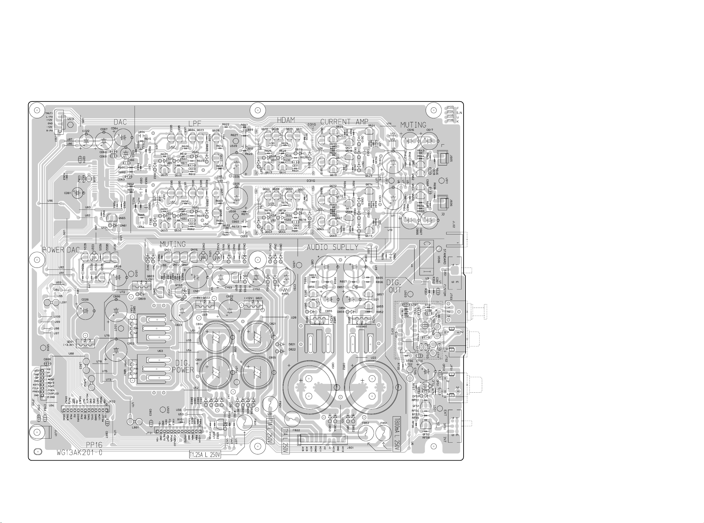
9. PARTS LOCATION
PP16
QD01
QD24- QD21
Q803 QN66 QY63
Q802 Q801
Q601 - Q608
Q651 - Q658QN65
QN04 QN02 QN01 QN06
Q822 Q821QY61 Q853 Q851 Q857 Q855
Q609 - Q614
Q659 - Q664 Q665 - Q672 Q673 Q674
Q615 - Q622 Q623 Q624 QN61 QN62
Q852
Q856
QN64 QN63
QT01
QF51 QF52QY62
1413
Page 13
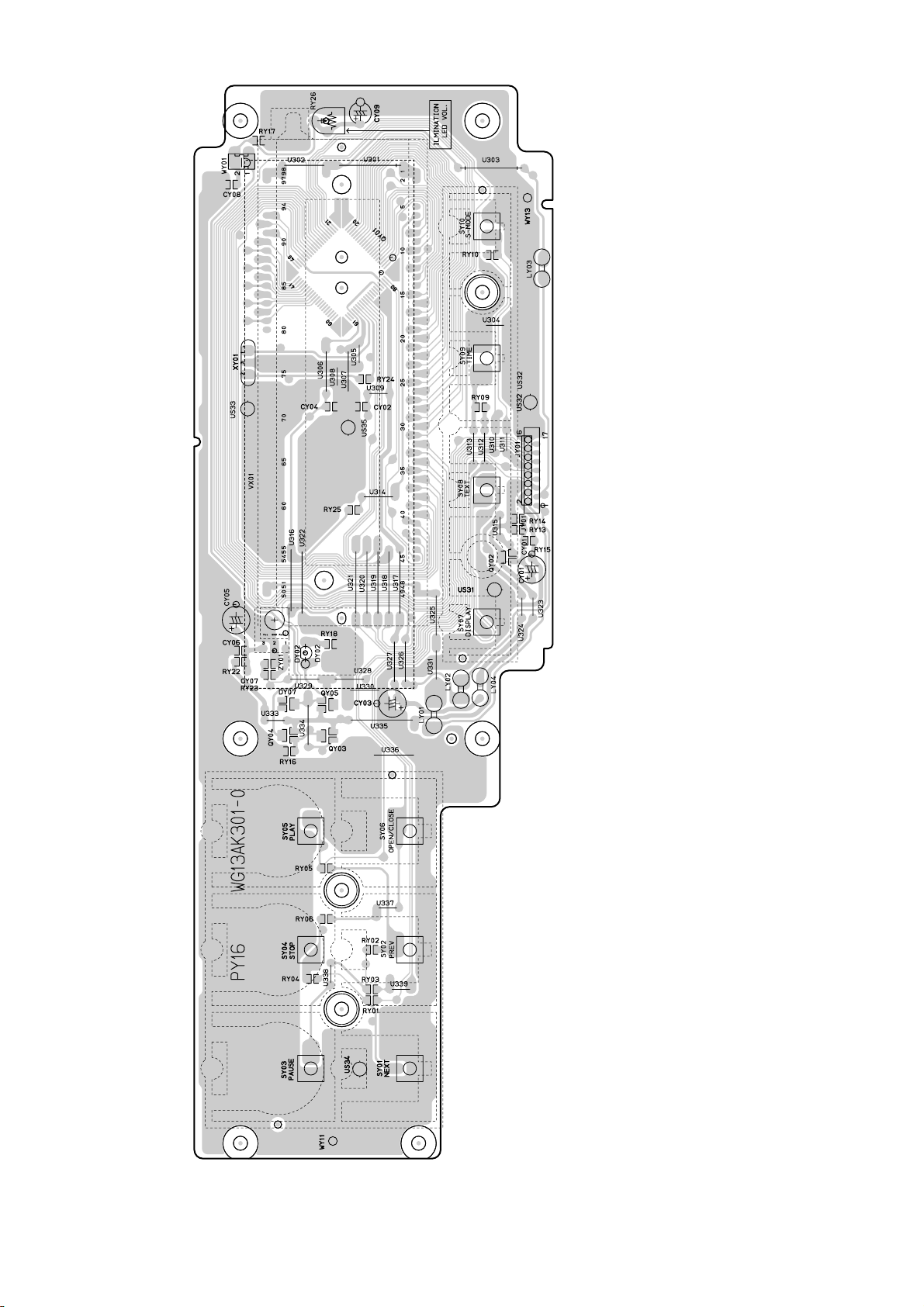
PY16
QY01
QY07
QY05
QY04 QY03
QY02
15
Page 14
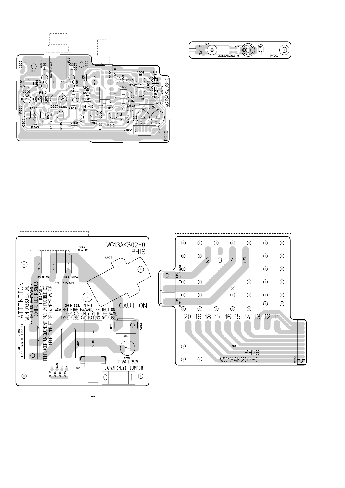
PR16
Q908
Q903
Q907
Q905
Q906
Q901
Q904
PY26
Q909
Q910
PH16
PH26
16
Page 15
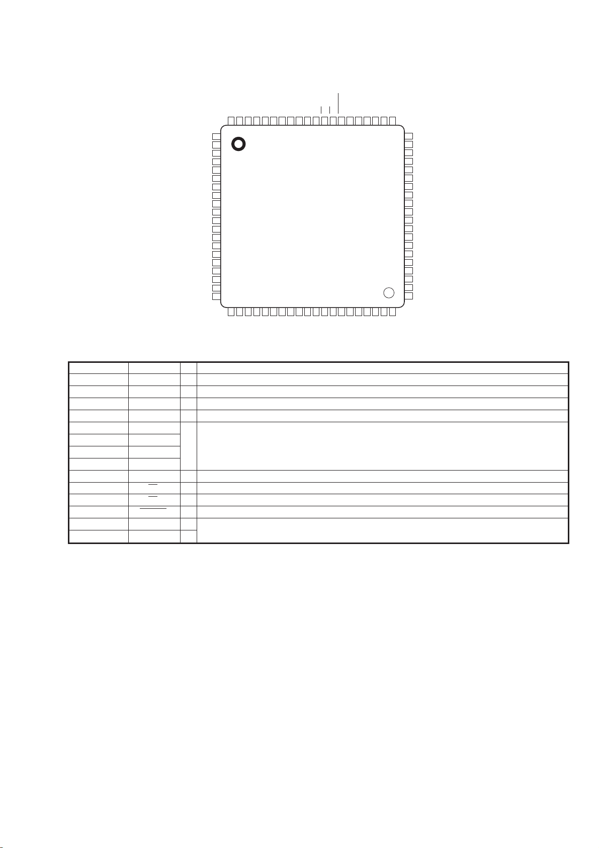
10. MICROPROCESSOR AND IC DATA
QY01 : ML9207-01
FL2
AD3
AD4
SEG1
SEG2
SEG3
SEG4
SEG5
SEG6
SEG7
SEG8
SEG9
SEG10
SEG11
SEG12
SEG13
SEG14
SEG15
SEG16
SEG17
SEG18
DISP2
NC
V
AD1
AD2
77
78
79
80
1
2
3
4
5
6
7
8
9
10
11
12
13
14
15
16
17
18
19
20
24
23
22
21
SEG22
SEG21
SEG20
SEG19
P4
V
75
76
26
25
SEG23
SEG24
P2
P3
73
74
28
27
SEG26
SEG25
72
29
SEG27
ML9207-01 Terminal Function
Pin Name FunctionPin No. I/O
3~37 SEG1~35 O FL display anode drive output pin
39~62 COM1~24 O FL display grid drive output pin
1,2, 79, 80 AD1~4 O FL display anode drive output pin
72~75 P1~4 O General port output pin
71 VDD
38, 78 VDISP1~2
64 GND
63, 76 VFL1~2
70 DA I Serial data input pin (positive logic)
69 CP I Shift clock input pin
68 CS I Chip select input pin
67 RESET I Reset input pin
65 OSC0 I
66 OSC1 O
VDD-GND: Power supply for logic block
VDISP-VFL: Power supply for FL display drive
For V
DD and VDISP, apply from same power source
Pin for self-oscillation
DA
VDDP1
70
71
31
30
SEG29
SEG28
CS
CP
68
69
33
32
SEG31
SEG30
OSC1
RESET
66
67
35
34
SEG33
SEG32
GND
OSC0
64
65
37
36
SEG35
SEG34
FL1
COM23
COM24
V
61
62
63
60
COM22
59
COM21
58
COM20
57
COM19
56
COM18
55
COM17
54
COM16
53
COM15
52
COM14
51
COM13
50
COM12
49
COM11
48
COM10
47
COM9
46
COM8
45
COM7
44
COM6
43
COM5
42
COM4
41
COM3
40
39
38
DISP1
V
COM2
COM1
17
Page 16
QD61 : CS4397
Reset - RST
Pin 1, Input
Function:
The device enters a low power mode and all internal state
machines registers are reset when low. When
high, the device will be in a normal operation mode .
clocked into SDATA via the serial clock
and the channel is determined by the Left/Right clock. The
required relationship between the Left/Right
clock, serial clock and serial data is defi ned by the Mode Control
Byte and the options are detailed inin
Figures 29-33
RST DESCRIPTION
0 Enabled
1 Normal operation mode
Digital Ground - DGND
Pins 6 and 9, Inputs
Function:
Digital ground reference.
Digital Power - VD
Pins 7 and 8, Input
Function:
Digital power supply. Typically 5.0 to 3.0 VDC.
Master Clock - MCLK
Pin 10, Input
Function:
The master clock frequency must be either 256x, 384x, 512x or
768x the input sample rate in Single
Speed Mode; either 128x, 192x 256x or 384x the input sample
rate in Double Speed Mode; or 64x, 96x
128x or 192x the input sample rate in Quad Speed Mode. Tables
4-6 illustrate the standard audio sample
rates and the required master clock frequencies.
Sample
Rate (kHz)
32 8.1920 12.2880 16.3840 24.5760
44.1 11.2896 16.9344 22.5792 33.8688
48 12.2880 18.4320 24.5760 36.8640
Table 4. Single Speed (16 to 50 kHz sample rates) Common Clock
Frequencies
Serial Clock - SCLK
Pin 11, Input
Function:
Clocks individual bits of serial data into the SDATA pin. The
required relationship between the Left/Right
clock, serial clock and serial data is defi ned by either the Mode
Control Byte in Control Port Mode or the
M0 - M4 pins in Hardware Mode. The options are detailed in
Figures 29-33
Left/Right Clock - LRCK
Pin 12, Input
Function:
The Left/Right clock determines which channel is currently being
input on the serial audio data input,
SDATA. The frequency of the Left/Right clock must be at the input
sample rate. Audio samples in
Left/Right sample pairs will be simultaneously output from the
digital-to-analog converter whereas
Right/Left pairs will exhibit a one sample period difference. The
required relationship between the
Left/Right clock, serial clock and serial data is defi ned by the
Mode Control Byte and the options are de-
tailed in Figures 29-33
256x 384x 512x 768x
MCLK (MHz)
Soft Mute - MUTE
Pin 15, Input
Function:
The analog outputs will ramp to a muted state when enabled. The
ramp requires 1152 left/right clock cy-
cles in Single Speed, 2304 cycles in Double Speed and 4608
cycles in Quad Speed mode. The bias volt-
age on the outputs will be retained and MUTEC will go active at
the completion of the ramp period.
The analog outputs will ramp to a normal state when this function
transitions from the enabled to disabled
state. The ramp requires 1152 left/right clock cycles in Single
Speed, 2304 cycles in Double Speed and
4608 cycles in Quad Speed mode. The MUTEC will release
immediately on setting MUTE = 1.
The converter analog outputs will mute when enabled. The bias
voltage on the outputs will be retained
and MUTEC will go active during the mute period.
Mute DESCRIPTION
0 Enabled
1 Normal operation mode
Control Port / Hardware Mode Select - C/H
Pin 16, Input
Function:
Determines if the device will operate in either the Hardware Mode
or Control Port Mode.
C/H DESCRIPTION
0 Hardware Mode Enabled
1 Control Port Mode Enabled
Mute Control - MUTEC
Pin 17, Output
Function:
The Mute Control pin goes low during power-up initialization,
reset, muting, master clock to left/right clock
frequency ratio is incorrect or power-down. This pin is intended to
be used as a control for an external mute
circuit to prevent the clicks and pops that can occur in any single
supply system. Use of Mute Control is not
mandatory but recommended for designs requiring the absolute
minimum in extraneous clicks and pops.
Analog Ground - AGND
Pins 18 and 21, Inputs
Function:
Analog ground reference.
Differential Analog Outpus - AOUTR- , AOUTR+ and AOUTL- ,
AOUTL+
Pins 19, 20, 23 and 24, Outputs
Function:
The full scale differential analog output level is specifi ed in the
Analog Characteristics specifi cations table.
Serial Audio Data - SDATA
Pin 13, Input
Function:
Serial audio data is input on this pin. The selection of the Digital
Interface Format is determined by set-
tings of the Mode select as detailed in Figures 29-33. The data is
Analog Power - VA
Pin 22, Input
Function:
Power for the analog and reference circuits. Typically 5VDC.
18
Page 17
QD61 : CS4397
Common Mode Voltage - CMOUT
Pin 25, Output Function:
Filter connection for internal bias voltage, typically 50% of VREF.
Capacitors must be connected from CMOUT to analog ground,
as shown in Figure 6. CMOUT has a typical source impedence
of 25 kΩ and any current drawn from this pin will alter device
performance
Reference Ground - FILT-
Pin 26, Input Function:
Ground reference for the internal sampling circuits. Must be
connected to analog ground.
Reference Filter - FILT+
Pin 27, Output Function:
Positive reference for internal sampling circuits. External
capacitors are required from FILT+ to analog ground, as shown in
Figure 6. FILT+ is not intended to supply external current.
Voltage Reference Input- VREF
Pin 28, Input Function:
Analog voltage reference. Typically 5VDC.
HARDWARE MODE
Mode Select - M0, M1, M2, M3, M4
Pins 2, 3, 4, 5 and 14, Inputs Function:
The Mode Select pins determine the operational mode of the
device as detailed in Tables 9-14. The op-tions include;
Selection of the Digital Interface Format which determines the
required relationship between the Left/Right clock, serial clock
and serial data as detailed in Figures 29-33 Selection of the
standard 15 µs/50 µs digital de-emphasis fi lter response, Figure
28, which requires re-confi guration of the digital fi lter to maintain
the proper fi lter response for 32, 44.1 or 48 kHz sample rates.
Selection of the appropriate clocking mode to match the input
sample rates. Access to the Direct Stream Digital Mode Access
to the 8x Interpolation Input Mode
CONTROL PORT MODE
Address Bit 0 / Chip Select - AD0 / CS
Pin 2, Input Function:
2
In I
C mode, AD0 is a chip address bit. CS is used to enable the
control port interface in SPI mode. The device will enter the SPI
mode at anytime a high to low transition is detected on this pin.
Once the device has entered the SPI mode, it will remain until
either the part is reset or undergoes a power-down cycle.
Address Bit 1 / Control Data Input - AD1/CDIN
Pin 3, Input Function:
In I2C mode, AD1 is a chip address bit. CDIN is the control data
input line for the control port interface in SPI mode.
Serial Control Interface Clock - SCL/CCLK
Pin 4, Input Function:
In I2C mode, SCL clocks the serial control data into or from
SDA/CDOUT.
In SPI mode, CCLK clocks the serial data into AD1/CDIN and out
of SDA/CDOUT.
Serial Control Data I/O - SDA/CDOUT
Pin 5, Input/Output Function:
In I2C mode, SDA is a data input/output. CDOUT is the control
data output for the control port interface in SPI mode.
M1 - Mode Select
Pin 14, Input Function:
This pin is not used in Control Port Mode and must be terminated
to ground.
SCLK
LRCK
SDATA
MCLK
CLOCK
DIVIDER
M4
(AD0/CS)
SERIAL INTERFACE
AND FORMAT SELECT
INTERPOLATION
INTERPOLATION
HARDWARE MODE CONTROL
M3 M2
(AD1/CDIN) (SCL/CCLK)
FILTER
FILTER
(CONTROL PORT)
M1
M0
(SDA/CDOUT)
SOFT MUTE
MULTI-BIT
∆Σ
MODULATOR
MULTI-BIT
∆Σ
MODULATOR
RESET MUTEC MUTE
DYNAMIC
ELEMENT
MATCHING
LOGIC
DYNAMIC
ELEMENT
MATCHING
LOGIC
DE-EMPHASIS
FILTER
SWITCHED
CAPACITOR-DAC
AND FILTER
SWITCHED
CAPACITOR-DAC
AND FILTER
VOLTAGE REFERENCE
VREF CMOUTFILT-
FILT+
AOUTL+
AOUTL-
AOUTR+
AOUTR-
19 20
Page 18
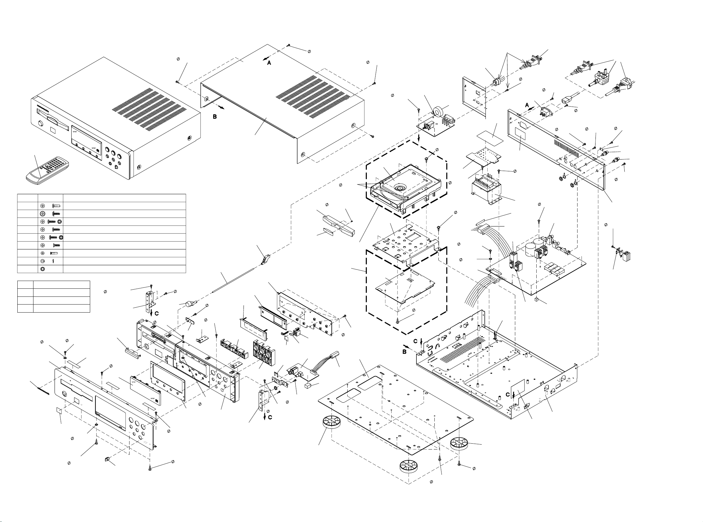
11. EXPLODED VIEW AND PARTS LIST
S
U
P
E
R
A
U
D
I
O
C
D
T100
SYMBOL ST YL E
5110
5126
5127
5128
5129
5150
5192
5404
5405
MARK
MATERIA L/ FINISH
(M)
STEEL /C OPPER
(U )
STEEL /BLACK
(A )
STEEL /CHROMATE
5405
3( M)
001B
017B
011B
PARTS NAME
+B .H .M .SCREW
+B .H .T APTITE SC REW W/ WASHER
+B .H .T APTITE SC REW (W /)
+B .H .T APTITE SC REW (B TYPE )
+B .H .T APTITE SC REW (W /T.L .WASHER )
+F .H .TAP TITE SCREW (B TY PE )
+P .H .M .SCR EW (M INUTE)
SPRING L OC K WASHER S
TOOT HED L OCK WASHER S
5129
3X8( M)
008B
5128
3X10( M)
003B
035Bx3
5128
3X8( M)
012B
5405
3( M)
5128
3X12( M)
x2
029B
5128
3X8( M)
020B
5128
3X10( M)
5126
3X10( M)
5128
3X8( M)
5126
3X8( M)
x4
x4
PY26
040B
x3
010B
x2
5405
3( M)
031B
5128
3X8( M)
5126
3X10( M)
002B
VX01
022B
009B
001D
030B
013B
021B
026B
PY16
016B
027B
5126
3X8( M)
007M
008M
015B
PR16
5128
3X8( M)
x2
5129
3X8( M)
1. 7X9( U)
S
U
P
E
R
A
U
D
I
O
Mecha Loader and
Mecha Traverse
Super Audio CD
PCB Module
014B
025G
032G
x2
5192
x2
C
D
L011
5405
2( M)
x2
5128
3X8( M)
x9
030G
5128
3X8( M)
x2
( 002M)
( 003M)
(006M)
5148
3X6( M)
x3
PH16
( 5110)
3X6( M)
x4
L003
( 5128)
2. 6X6( U)
x4
5129
3X8( M)
5128
3X8( M)
x9
PH26
5129
3X8( M)
x4
5110
3X6( M)
5405
3( M)
L013
/K/L ONLY
908G
024G
033G
x2
5128
3X10( M)
x4
L012
022L
002G
5128
3X8( M)
J001
925G
5126
3X8( M)
x3
L001
023G
x4
035Gx2
x2
027G
W002
5129
3X8( M)
5148
3X6( M)
x7
021L
x3
022G
001G
/F Only
5128
3X8( M) x2
5127
3X8( M)
PP16
031Gx2
/K/S ONLY
/S Only
5127
3X8( M)
x4
035G
W001
/N Only
5128
3X5( M)
920G
J608
5126
3X8( M)
901G
5110
3X8( M)
J607
2221
Page 19
POS.
NO
VERS.
COLOR
PART NO.
(FOR EUR)
DESCRIPTION
PART NO.
(MJI)
POS.
NO
VERS.
COLOR
PART NO.
(FOR EUR)
DESCRIPTION
PART NO.
(MJI)
001B GOLD 13AK248110 FRONT AL PANEL GOLD 13AK248110
001B BLACK 13AK248010 FRONT AL PANEL BLACK 13AK248010
002B GOLD 13AK105120 CHASSIS
13AK105120
FRONT MOLD PANEL GOLD
002B BLACK 13AK105020 CHASSIS
13AK105020
FRONT MOLD PANEL BLACK
003B 13AK355010 LENS ESCUTCHEON 13AK355010
011B 01AK251010 BADGE SUPER AUDIO CD LOGO 01AK251010
012B 01AK158020 WINDOW 01AK158020
015B 382K355010 LENS 382K355010
017B 24AW251010 BADGE NEW MARANTZ LOGO 24AW251010
020B GOLD 05AK270110 BUTTON POWER GOLD 05AK270110
020B BLACK 05AK270010 BUTTON POWER BLACK 05AK270010
021B GOLD 13AK270110 BUTTON 6 GOLD 13AK270110
021B BLACK 13AK270010 BUTTON 6 BLACK 13AK270010
022B GOLD 13AK270120 BUTTON 4 GOLD 13AK270120
022B BLACK 13AK270020 BUTTON 4 BLACK 13AK270020
029B GOLD 284T154250 KNOB PHONE VOLUME GOLD 284T154250
029B BLACK 284T154310 KNOB PHONE VOLUME BLACK 284T154310
030B 376K121010 LINK FOR POWER BUTTON 376K121010
040B GOLD 13AK063120 ESCUTCHEON GOLD 13AK063120
040B BLACK 13AK063020 ESCUTCHEON BLACK 13AK063020
032G 183J057010 LEG FRONT 183J057010
033G 183J057110 LEG REAR 183J057110
908G /K/L nsp BUSHING FOR MAINS CORD 450H259010
002M 13AK304010 MECHA LOADER AND
13AK304010
MECHA TRAVERSE
006M ZK13AK0020 SUPER AUDIO CD PCB MODULE ZK13AK0020
007M GOLD 13AK063110 ESCUTCHEON
13AK063110
FOR CD TRAY GOLD
007M BLACK 13AK063010 ESCUTCHEON
13AK063010
FOR CD TRAY BLACK
008M 392K063160 ESCUTCHEON
392K063160
SUPER AUDIO CD LOGO
J001 /F/N/S YJ04002550 JACK MAINS INLET TYPE HF-301 YJ04002550
J607 YT02011290 TERMINAL
YT02011290
EW-2560T-LH-W FOR L-CH
J608 YT02011280 TERMINAL
YT02011280
EW-2560T-LH-R FOR R-CH
L003 FC50230010 FERRITE CORE TFCK-23-11-14
FC50230010
FOR W002, W003
L011 FC50270040 FERRITE CORE USB-4 FOR W901 FC50270040
L012 FC90280010 FERRITE CORE
FC90280010
HF70SH28*2*10 FOR WF04
L013 FC90280010 FERRITE CORE
FC90280010
HF70SH28*2*10 FOR WF07
W002 /K nsp MAINS CORD
YC01800880
CCEE APP.AC250V 10A+ VAR2P
W002 /L nsp MAINS CORD
YC01800950
CCEE APP.AC250V 10A+ VAR2P
WF04 YU25110520 JUMPER LEAD JF01-CY251
YU25110520
FFC 1MM-PITCH 25P
WF05 YU25110520 JUMPER LEAD JF01-CY252
YU25110520
FFC 1MM-PITCH 25P
WF07 YU17120520 JUMPER LEAD JF03-JY01
YU17120520
FFC 1MM-PITCH 17P
PACKING
001T /F nsp USER GUIDE SA8400 /F 13AK851110
001T /K/L/S nsp USER GUIDE SA8400 /K/L/S 13AK851350
001T /N 13AK851310 USER GUIDE SA8400 /N 13AK851310
T100 ZK13AK0010 REMOTE CONTROLLER
ZK13AK0010
RC8400SA
W001 /F nsp MAINS CORD
ZC01802080
AC 125V 12A FOR F OFC
W001 /N ZC01803080 MAINS CORD
ZC01803080
AC 250V 10A CLASS2
W001 /S nsp MAINS CORD
ZC01804100
AC 250V 10A FOR UK
NOT STANDARD
SPARE PART
001S nsp PACKING CASE 13AK801010
002S nsp CUSHION L/R 02AJ809010
001D GOLD nsp LID TOP COVER GOLD 02AJ257120
001D BLACK nsp LID TOP COVER BLACK 02AJ257020
NOTE : "nsp" PART IS LISTED FOR REFERENCE ONLY, MARANTZ WILL NOT SUPPLY THESE PARTS.
23
Page 20
12. ELECTRICAL PARTS LIST
ASSIGNMENT OF COMMON PARTS CODES.
RESISTORS
R : 1) GD05 × × × 140, Carbon film fixed resistor, ±5% 1/4W
R : 2) GD05 × × × 160, Carbon film fixed resistor, ±5% 1/6W
Examples ;
Resistance value
➀
0.1 Ω.... 001 10 Ω .... 100 1 kΩ .... 102 100 kΩ.... 104
0.5 Ω.... 005 18 Ω .... 180 2.7 kΩ .... 272 680 kΩ .... 684
1 Ω .... 010 100 Ω .... 101 10 kΩ .... 103 1 MΩ.... 105
6.8 Ω.... 068 390 Ω .... 391 22 kΩ .... 223 4.7 MΩ.... 475
Note : Please distinguish 1/4W from 1/6W by the shape of parts
used actually.
CAPACITORS
C : CERAMIC CAP.
3) DD1 × × × × 370, Ceramic capacitor
Examples ;
Tolerance (Capacity deviation)
➁
±0.25 pF .... 0
Tolerance of COMMON PARTS handled here are as follows :
C : CERAMIC CAP.
Examples ;
C : 5) ELECTROLY CAP. ( ), 6) FILM CAP. ( )
Examples ;
0.5 pF 5 pF .... ±0.25 pF
Capacity value
➂
0.5 pF ....005 3 pF .... 030 100 pF .... 101
1.5 pF ....015 47 pF .... 470 560 pF .... 561
4) DK16 × × × 300, High dielectric constant ceramic
Capacity value
➃
100 pF .... 101 1000 pF ....102 10000 pF .... 103
470 pF .... 471 2200 pF ....222
5) EA × × × × × × 10, Electrolytic capacitor
Capacity value
➄
0.1 µF.... 104 4.7 µF .... 475 100 µF ....107
0.33 µF.... 334 10 µF .... 106 330 µF ....337
Working voltage
➅
{
➂
{
{
➅
Resistance value
Disc type
Temp.coeff.P350 N1000, 50V
Capacity value
Tolerance
capacitor
Disc type
Temp.chara. 2B4, 50V
Capacity value
One-way lead type, Tolerance ±20%
Working voltage
Capacity value
2200 µF ....228
➀
{
➁
±0.5 pF .... 1
±5% .... 5
6 pF 10 pF .... ±0.5 pF
12 pF 560 pF .... ±5%
1 pF .... 010 10 pF .... 100 220 pF .... 221
➃
{
➄
1 µF....105 22 µF .... 226 1100 µF ....118
6.3V.... 006 25V .... 025
10V .... 010 35V .... 035
16V .... 016 50V .... 050
NOTE ON SAFETY FOR FUSIBLE RESISTOR :
The suppliers and their type numbers of fusible resistors
are as follows;
1. KOA Corporation
Part No. (MJI) Type No. (KOA) Description
NH05 × × × 140 RF25S × × × × ΩJ(±5% 1/4W)
NH05 × × × 120 RF50S × × × × ΩJ(±5% 1/2W)
NH85 × × × 110 RF73B2A × × × × ΩJ(±5% 1/10W)
NH95 × × × 140 RF73B2E × × × × ΩJ(±5% 1/4W)
2. Matsushita Electronic Components Co., Ltd
Part No. (MJI) Type No. (MEC) Description
NF05 × × × 140 ERD-2FCJ × × × (±5% 1/4W)
RF05 × × × 140
NF02 × × × 140
RF02 × × × 140
Examples ;
{
Resistance value
ERD-2FCG
{
Resistance value
Resistance value
0.1 Ω.... 001 10 Ω .... 100 1 kΩ .... 102 100 kΩ.... 104
0.5 Ω.... 005 18 Ω .... 180 2.7 kΩ .... 272 680 kΩ .... 684
1 Ω .... 010 100 Ω .... 101 10 kΩ .... 103 1 MΩ.... 105
6.8 Ω.... 068 390 Ω .... 391 22 kΩ .... 223 4.7 MΩ.... 475
{
Resistance value
(0.1 Ω − 10 kΩ)
× × × (±2% 1/4W)
{
Resistance value
ABBREVIATION AND MARKS
ANT. : ANTENNA BATT. : BATTERY
CAP. : CAPACITOR CER. : CERAMIC
CONN. : CONNECTING DIG. : DIGITAL
HP : HEADPHONE MIC. : MICROPHONE
µ-PRO : MICROPROCESSOR REC. : RECORDING
RES. : RESISTOR SPK : SPEAKER
SW : SWITCH TRANSF. : TRANSFORMER
TRIM. : TRIMMING TRS. : TRANSISTOR
VAR. : VARIABLE X’TAL : CRYSTAL
NOTE ON FUSE :
Regarding to all parts of parts code FS20xxx2xx, replace
only with Wickmann-Werke GmbH, Type 372 non glass type
fuse.
6) DF15 × × × 350 Plastic film capacitor
DF15 × × × 310 One-way type, Mylar ±5% 50V
DF16 × × × 310 Plastic film capacitor
Examples ;
Capacity value
➆
0.001 µF (1000 pF) ....... 102 0.1 µF .... 104
0.0018 µF ........................ 182 0.56 µF .... 564
0.01 µF........................ 103 1 µF ....105
0.015 µF ........................ 153
: 1) The above CODES ( R , R , C , C and
NOTE
C ) are omitted on the schematic diagram in some
case.
2) On the occasion, be confirmed the common parts on
the parts list.
3) Refer to “Common Parts List” for the other common
parts (RI05, DD4, DK4).
➆
{
One-way type, Mylar ±10% 50V
Capacity value
NOTE ON SAFETY :
Symbol Fire or electrical shock hazard. Only original
parts should be used to replaced any part marked with
symbol . Any other component substitution (other
than original type), may increase risk of fire or electrical
shock hazard.
010728MIT
24
Page 21

POS.
NO
VERS.
COLOR
PART NO.
(FOR EUR)
DESCRIPTION
PART NO.
(MJI)
POS.
NO
VERS.
COLOR
PART NO.
(FOR EUR)
DESCRIPTION
PART NO.
(MJI)
PH16-POWER SWITCH
CIRCUIT BOARD
FH01 /K/L/N /SFS20125200 FUSE T1.25A 250V VDE SEMKO FS20125200
GH01 DF77103500 FILM 0.01µF M 250V AC DF77103500
JH01 YP04000760 PLUG CONNECTOR B2P3-VH YP04000760
JH02 /F/N/S YP04000760 PLUG CONNECTOR B2P3-VH YP04000760
JH03 /K/L nsp PLUG CONNECTOR B3P5-VH YP04000920
SH01 SP01012480 PUSH SWITCH
SP01012480
ESB92S94B TV-5 1.5MM
SH02 /K/L nsp VOLTAGE SELECTOR SDKGA4 SS02021510
PH26-TRANSFORMER
CIRCUIT BOARD
JH04 /F/N/S YP04000760 PLUG CONNECTOR B2P3-VH YP04000760
JH05 /K/L nsp PLUG CONNECTOR B3P5-VH YP04000920
L001 /F nsp TRANSF. EI66-30 AC100V F TS16679010
L001 /K/L nsp TRANSF. EI66-30 AC110V/220 K TS16679020
L001 /N/S TS16679030 TRANSF. EI66-30 AC230V S TS16679030
PP16-POWER/AUDIO (L R)
CIRCUIT BOARD
PP16-CAPACITORS
C601 OF55182570 FILM DTG 1800pF 100V OF55182570
C602 OF55331570 FILM DTG 330pF 100V OF55331570
C604 OF55121560 FILM DAMG 120pF 630V OF55121560
C605 nsp ELECT. 220µF 16V ARA
C606 nsp ELECT. 220µF 16V ARA
CERAFINE
CERAFINE
OA22701650
OA22701650
C609 OF55122570 FILM DTG 1200pF 100V OF55122570
C610 OF55561570 FILM DTG 560pF 100V OF55561570
C612 OF55681570 FILM DTG 680pF 100V OF55681570
C613 nsp ELECT. 220µF 16V ARA
C614 nsp ELECT. 220µF 16V ARA
CERAFINE
CERAFINE
OA22701650
OA22701650
C616 nsp ELECT. 100µF 25V ARS OA10702540
C651 OF55182570 FILM DTG 1800pF 100V OF55182570
C652 OF55331570 FILM DTG 330pF 100V OF55331570
C654 OF55121560 FILM DAMG 120pF 630V OF55121560
C659 OF55122570 FILM DTG 1200pF 100V OF55122570
C660 OF55561570 FILM DTG 560pF 100V OF55561570
C662 OF55681570 FILM DTG 680pF 100V OF55681570
C666 nsp ELECT. 100µF 25V ARS OA10702540
C801 OA68801620 ELECT. 6800µF 16V ± 20% RA-2 OA68801620
C802 nsp ELECT. 3300µF M 6.3V RA-2 OA33800620
C804 nsp ELECT. 3300µF 16V RA2 TYPE OA33801620
C805 nsp ELECT. 6800 µF 16V RA2 OA68801620
C806 nsp ELECT. 3300µF M 6.3V RA-2 OA33800620
C809 nsp ELECT. 1000µF 10V M RA-2 OA10801020
C821 OA47802520 ELECT. 4700µF 25V RA-2 OA47802520
C822 nsp ELECT. 2200µF 16V OA22801620
C823 nsp ELECT. 2200µF 16V OA22801620
C851 OB33802510 ELECT. 3300µF 25V ±20%
C852 OB33802510 ELECT. 3300µF 25V ±20%
FOR HIFI
FOR HIFI
OB33802510
OB33802510
C855 nsp ELECT. 10µF 25V ARA OA10602550
C856 nsp ELECT. 10µF 25V ARA OA10602550
C857 nsp ELECT. 470 µF M 16V ARA OA47701650
C858 nsp ELECT. 470 µF M 16V ARA OA47701650
CD21 nsp ELECT. 10 µF 63V RA-2 OA10606320
CD22 nsp ELECT. 100 µF M 10V RA-2 OA10701020
CD26 nsp ELECT. 220 µF M 25V RA-2 OA22702520
CD61 nsp ELECT. 100 µF M 25V RA-2 OA10702520
CD64 nsp ELECT. 100 µF M 25V RA-2 OA10702520
CD65 nsp ELECT. 10µF 25V ARA OA10602550
CD67 nsp ELECT. 100µF 10V ARA OA10701050
CF54 nsp ELECT. 10 µF 63V RA-2 OA10606320
CN01 nsp ELECT. 1000 µF M 25V RA-2 OA10802520
CN02 nsp ELECT. 1 µF M100V RA-2 OA10510020
CN03 nsp ELECT. 4.7 µF M 50V RA-2 OA47505020
CN04 DF15104350 FILM 0.1µF J N 50V DF15104350
CT05 nsp ELECT. 100µF 25V ARS OA10702540
CY51 OA22705020 ELECT. 220 µF M 50V RA-2 OA22705020
CY52 OA22705020 ELECT. 220 µF M 50V RA-2 OA22705020
CY63 nsp ELECT. 100 µF M 50V RA-2 OA10705020
PP16-RESISTORS
R615 nsp 5.1kΩ ±5% 1/6W GD05512160
R644 nsp 75Ω ±5% 1/6W GD05750160
R645 nsp 75Ω ±5% 1/6W GD05750160
R665 nsp 5.1kΩ ±5% 1/6W GD05512160
R694 nsp 75Ω ±5% 1/6W GD05750160
R695 nsp 75Ω ±5% 1/6W GD05750160
RT03 nsp 75Ω ±5% 1/6W GD05750160
RY55 NH05100140 FUSIBLE 10Ω J 1/4W NH05100140
PP16-RESISTORS (COMMON)
CARBON FILM FIXED RES.
±5% 1/6W : R351 R352 R601-R614
R622-R641 R643 R647 R651-R664
R672-R691 R693 R697 R851-R858
R901-R926 RD22-RD25
RD63-RD65 RF51-RF58
RN01-RN06 RN09 RN10
RN61-RN64 RT01 RT02
RT04-RT06 RY51 RY56-RY61
PP16-SEMICONDUCTORS
D601
nsp DIODE HD20002000
D613 1SS176 MA165 1SS254 30V 0.1A
D651
nsp DIODE HD20002000
D663 1SS176 MA165 1SS254 30V 0.1A
D801
HD20055100 DIODE SHOTTKY HD20055100
D809 11EQS10 1A 100V
D821 HD20002710 DIODE 1D3 1A 200V HD20002710
D822 HD20002710 DIODE 1D3 1A 200V HD20002710
D851
HD20055100 DIODE SHOTTKY HD20055100
D854 11EQS10 1A 100V
D856 HD30021010 ZENER DIODE HZ6L 3 6.2V HD30021010
D857 HD30021010 ZENER DIODE HZ6L 3 6.2V HD30021010
D858 nsp DIODE
HD20002000
1SS176 MA165 1SS254 30V 0.1A
D859 nsp DIODE
HD20002000
1SS176 MA165 1SS254 30V 0.1A
DF51 nsp DIODE
HD20002000
1SS176 MA165 1SS254 30V 0.1A
DN01 HD20002710 DIODE 1D3 1A 200V HD20002710
DN02 HD20002710 DIODE 1D3 1A 200V HD20002710
DN05 nsp DIODE 1D3 1A 200V HD20002710
DN06 HD30471000 ZENER DIODE 4.7V HD30471000
DN07 nsp DIODE
HD20002000
1SS176 MA165 1SS254 30V 0.1A
DN11 nsp DIODE
HD20002000
1SS176 MA165 1SS254 30V 0.1A
DN12 nsp DIODE
HD20002000
1SS176 MA165 1SS254 30V 0.1A
DY11 HD30471000 ZENER DIODE 4.7V HD30471000
DY51 HD20002710 DIODE 1D3 1A/200V HD20002710
DY52 HD20002710 DIODE 1D3 1A/200V HD20002710
DY61 HD32701000 ZENER DIODE 27V HD32701000
DY65 HD32701000 ZENER DIODE 27V HD32701000
Q601 HF203691B0 F.E.T.
HF203691B0
2SK369 BL VGDS-40V PD0.4W
Q602 HF203691B0 F.E.T.
HF203691B0
2SK369 BL VGDS-40V PD0.4W
Q603 HT322402A0 TRS. 2SC2240 GR OR BL HT322402A0
Q604 HT109702A0 TRS. 2SA970 GR OR BL HT109702A0
Q605 HT109702A0 TRS. 2SA970 GR OR BL HT109702A0
NOTE : "nsp" PART IS LISTED FOR REFERENCE ONLY, MARANTZ WILL NOT SUPPLY THESE PARTS.
25
Page 22

POS.
NO
VERS.
COLOR
PART NO.
(FOR EUR)
DESCRIPTION
PART NO.
(MJI)
POS.
NO
VERS.
COLOR
PART NO.
(FOR EUR)
DESCRIPTION
PART NO.
(MJI)
Q606 HT322402A0 TRS. 2SC2240 GR OR BL HT322402A0
Q607 HF201701H0 F.E.T. 2SK170 V RANK HF201701H0
Q608 HF100741H0 F.E.T. 2SJ74 V RANK HF100741H0
Q609 HF203691B0 F.E.T.
HF203691B0
2SK369 BL VGDS-40V PD0.4W
Q610 HF203691B0 F.E.T.
HF203691B0
2SK369 BL VGDS-40V PD0.4W
Q611 HT322402A0 TRS. 2SC2240 GR OR BL HT322402A0
Q612 HT109702A0 TRS. 2SA970 GR OR BL HT109702A0
Q613 HT109702A0 TRS. 2SA970 GR OR BL HT109702A0
Q614 HT322402A0 TRS. 2SC2240 GR OR BL HT322402A0
Q615 HF201701H0 F.E.T. 2SK170 V RANK HF201701H0
Q616 HF100741H0 F.E.T. 2SJ74 V RANK HF100741H0
Q617 HT109702A0 TRS. 2SA970 GR OR BL HT109702A0
Q618 HT109702A0 TRS. 2SA970 GR OR BL HT109702A0
Q619 HT109702A0 TRS. 2SA970 GR OR BL HT109702A0
Q620 HT322402A0 TRS. 2SC2240 GR OR BL HT322402A0
Q621 HT322402A0 TRS. 2SC2240 GR OR BL HT322402A0
Q622 HT322402A0 TRS. 2SC2240 GR OR BL HT322402A0
Q623 HT322402A0 TRS. 2SC2240 GR OR BL HT322402A0
Q624 HT109702A0 TRS. 2SA970 GR OR BL HT109702A0
Q651 HF203691B0 F.E.T.
HF203691B0
2SK369 BL VGDS-40V PD0.4W
Q652 HF203691B0 F.E.T.
HF203691B0
2SK369 BL VGDS-40V PD0.4W
Q653 HT322402A0 TRS. 2SC2240 GR OR BL HT322402A0
Q654 HT109702A0 TRS. 2SA970 GR OR BL HT109702A0
Q655 HT109702A0 TRS. 2SA970 GR OR BL HT109702A0
Q656 HT322402A0 TRS. 2SC2240 GR OR BL HT322402A0
Q657 HF201701H0 F.E.T. 2SK170 V RANK HF201701H0
Q658 HF100741H0 F.E.T. 2SJ74 V RANK HF100741H0
Q659 HF203691B0 F.E.T.
HF203691B0
2SK369 BL VGDS-40V PD0.4W
Q660 HF203691B0 F.E.T.
HF203691B0
2SK369 BL VGDS-40V PD0.4W
Q661 HT322402A0 TRS. 2SC2240 GR OR BL HT322402A0
Q662 HT109702A0 TRS. 2SA970 GR OR BL HT109702A0
Q663 HT109702A0 TRS. 2SA970 GR OR BL HT109702A0
Q664 HT322402A0 TRS. 2SC2240 GR OR BL HT322402A0
Q665 HF201701H0 F.E.T. 2SK170 V RANK HF201701H0
Q666 HF100741H0 F.E.T. 2SJ74 V RANK HF100741H0
Q667 HT109702A0 TRS. 2SA970 GR OR BL HT109702A0
Q668 HT109702A0 TRS. 2SA970 GR OR BL HT109702A0
Q669 HT109702A0 TRS. 2SA970 GR OR BL HT109702A0
Q670 HT322402A0 TRS. 2SC2240 GR OR BL HT322402A0
Q671 HT322402A0 TRS. 2SC2240 GR OR BL HT322402A0
Q672 HT322402A0 TRS. 2SC2240 GR OR BL HT322402A0
Q673 HT322402A0 TRS. 2SC2240 GR OR BL HT322402A0
Q674 HT109702A0 TRS. 2SA970 GR OR BL HT109702A0
Q801 HC3690521F IC REG. BA05T 5V/1A TO220 HC3690521F
Q802 HC3690521F IC REG. BA05T 5V/1A TO220 HC3690521F
Q803 HC3850509F IC REG. NJM78M05F HC3850509F
Q821 HC3891209F IC REG. NJM7812FA +12V HC3891209F
Q822 HC3890809F IC REG. NJM7808F HC3890809F
Q851 HF202461C0 F.E.T. 2SK246 GR HF202461C0
Q852 HT41415100 TRS. 2SD1415A HT41415100
Q853 HT322402A0 TRS. 2SC2240 GR OR BL HT322402A0
Q855 HF202461C0 F.E.T. 2SK246 GR HF202461C0
Q856 HT21020100 TRS. 2SB1020A HT21020100
Q857 HT109702A0 TRS. 2SA970 GR OR BL HT109702A0
QD01 HC36J3321F IC REG. BA033T 3.3V FOR
HC36J3321F
DMAINS POWER
QD21 BA20004000 DIG. TRS. DTC114TS/UN4215 10K BA20004000
QD22 BA20004000 DIG. TRS. DTC114TS/UN4215 10K BA20004000
QD23 HT109702A0 TRS. 2SA970 GR OR BL HT109702A0
QD24 HT328782A0 TRS. 2SC2878 A OR B HT328782A0
QD61 HC10008880 IC CS4397
HC10008880
DSD/PCD DAC 24BIT 192K
QF51 HT10001000 TRS.
HT10001000
2SA1048 2SA933S 2SA1267 ETC.
QF52 HT30001000 TRS.
HT30001000
2SC2458 2SC1740S 2SC3199
ETC.
QN01 HT30001000 TRS.
HT30001000
2SC2458 2SC1740S 2SC3199
ETC.
QN02 BA20004000 DIG. TRS. DTC114TS/UN4215 10K BA20004000
QN04 HT10001000 TRS.
HT10001000
2SA1048 2SA933S 2SA1267 ETC.
QN06 HT30001000 TRS.
HT30001000
2SC2458 2SC1740S 2SC3199
ETC.
QN61 HT328782A0 TRS. 2SC2878 A OR B HT328782A0
QN62 HT328782A0 TRS. 2SC2878 A OR B HT328782A0
QN63 HT328782A0 TRS. 2SC2878 A OR B HT328782A0
QN64 HT328782A0 TRS. 2SC2878 A OR B HT328782A0
QN66 BA20004000 DIG. TRS. DTC114TS/UN4215 10K BA20004000
QT01
QY61 HT10001000 TRS.
HC700400D0
IC 74HC04 HI-SPEED C-MOS
HC700400D0
HT10001000
2SA1048 2SA933S 2SA1267 ETC.
QY62 HT30001000 TRS.
HT30001000
2SC2458 2SC1740S 2SC3199
ETC.
QY63 BA20004000 DIG. TRS. DTC114TS/UN4215 10K BA20004000
PP16-MISCELLANEOUS
F801 FS20125200 FUSE T1.25A 250V VDE SEMKO FS20125200
F821 FS20100200 FUSE FUSE 1A 250V SEMKO VDE FS20100200
F822 FS20100200 FUSE FUSE 1A 250V SEMKO VDE FS20100200
F851 FS20080200 FUSE T800MA 250V VDE SEMCO FS20080200
F852 FS20080200 FUSE T800MA 250V VDE SEMCO FS20080200
JF51 YT02020890 TERMINAL 2P CINCH PIN JACK YT02020890
JT02 YT02010790 TERMINAL
YT02010790
14x14 RA 1L1P BLK AU FLM-GND
JT03 YJ15000210 OPT. CONNECTOR JFJ300
YJ15000210
OUTPUT
L801 FC90050130 FERRITE BEAD BL02RN2-R62T2 FC90050130
L802 FC90050130 FERRITE BEAD BL02RN2-R62T2 FC90050130
L803 FC90050130 FERRITE BEAD BL02RN2-R62T2 FC90050130
LD01 FC90050130 FERRITE BEAD BL02RN2-R62T2 FC90050130
LT01 TP41042030 PULSE TRNSF.
TP41042030
TPS247MN-0386AN
LT02 FC90050130 FERRITE BEAD BL02RN2-R62T2 FC90050130
LT03 FC90050130 FERRITE BEAD BL02RN2-R62T2 FC90050130
LT04 FC90050130 FERRITE BEAD BL02RN2-R62T2 FC90050130
S351 SS02021150 SLIDE SWITCH FILTER SWITCH
SS02021150
STANDARD/CUSTOM
SF51 SS02021150 SLIDE SWITCH RC-5 INT/EΩ T SS02021150
PR16-HEADPHONE
CIRCUIT BOARD
PR16-CAPACITORS
C901 OA47602520 ELECT. 47 µF M 25V RA-2 OA47602520
C902 OA47602520 ELECT. 47 µF M 25V RA-2 OA47602520
C903 OA22702520 ELECT. 220 µF M 25V RA-2 OA22702520
C904 OA22702520 ELECT. 220 µF M 25V RA-2 OA22702520
C905 OA47602520 ELECT. 47 µF M 25V RA-2 OA47602520
C906 OA47602520 ELECT. 47 µF M 25V RA-2 OA47602520
PR16-RESISTORS
R901 nsp 1.2kΩ ±5% 1/6W GD05122160
R902 nsp 1.2kΩ ±5% 1/6W GD05122160
R903 nsp 33Ω ±5% 1/6W GD05330160
R904 nsp 33Ω ±5% 1/6W GD05330160
R905 nsp 33Ω ±5% 1/6W GD05330160
R906 nsp 33Ω ±5% 1/6W GD05330160
R907 nsp 1.5kΩ ±5% 1/6W GD05152160
R908 nsp 1.5kΩ ±5% 1/6W GD05152160
R909 nsp 1.5kΩ ±5% 1/6W GD05152160
R910 nsp 1.5kΩ ±5% 1/6W GD05152160
NOTE : "nsp" PART IS LISTED FOR REFERENCE ONLY, MARANTZ WILL NOT SUPPLY THESE PARTS.
26
Page 23

POS.
NO
VERS.
COLOR
PART NO.
(FOR EUR)
DESCRIPTION
PART NO.
(MJI)
POS.
NO
VERS.
COLOR
PART NO.
(FOR EUR)
DESCRIPTION
PART NO.
(MJI)
R911 nsp 33Ω ±5% 1/6W GD05330160
R912 nsp 33Ω ±5% 1/6W GD05330160
R913 nsp 33Ω ±5% 1/6W GD05330160
R914 nsp 33Ω ±5% 1/6W GD05330160
R915 nsp 100kΩ ±5% 1/6W GD05104160
R916 nsp 100kΩ ±5% 1/6W GD05104160
R917 nsp 100Ω ±5% 1/6W GD05101160
R918 nsp 100Ω ±5% 1/6W GD05101160
R919 nsp 8.2kΩ ±5% 1/6W GD05822160
R920 nsp 8.2kΩ ±5% 1/6W GD05822160
R921 nsp 4.7kΩ ±5% 1/6W GD05472160
R922 nsp 4.7kΩ ±5% 1/6W GD05472160
R923 nsp 4.7kΩ ±5% 1/6W GD05472160
R924 nsp 4.7kΩ ±5% 1/6W GD05472160
R925 nsp 4.7kΩ ±5% 1/6W GD05472160
R926 nsp 4.7kΩ ±5% 1/6W GD05472160
R930 RM01031220 VARIABLE RK09L12B0 10K B
RM01031220
D-CUT NORMAL
PR16-SEMICONDUCTORS
D901
nsp DIODE HD20002000
D904 1SS176 MA165 1SS254 30V 0.1A
Q901 HC10111090 IC NJM2114D
HC10111090
DUAL LOW NOISE OP-AMP
Q903 HT321201B0 TRS. 2SC2120 Y HT321201B0
Q904 HT321201B0 TRS. 2SC2120 Y HT321201B0
Q905 HT109501A0 TRS. 2SA950 GR OR R HT109501A0
Q906 HT109501A0 TRS. 2SA950 GR OR R HT109501A0
Q907 HT328782A0 TRS. 2SC2878 A OR B HT328782A0
Q908 HT328782A0 TRS. 2SC2878 A OR B HT328782A0
Q909 HT328782A0 TRS. 2SC2878 A OR B HT328782A0
Q910 HT328782A0 TRS. 2SC2878 A OR B HT328782A0
PR16-MISCELLANEOUS
J903 YJ01003870 H.P JACK HLJ0540-01-410 BLK YJ01003870
L901 FC90050130 FERRITE BEAD BL02RN2-R62T2 FC90050130
L902 FC90050130 FERRITE BEAD BL02RN2-R62T2 FC90050130
PY16-DISPLAY SW
CIRCUIT BOARD
PY16-CAPACITORS
CY01 nsp ELECT. 47 µF M 25V RA-2 OA47602520
CY02 nsp CER. 0.1 µF Z 50V F DK98104200
CY03 nsp ELECT. 47 µF M 25V RA-2 OA47602520
CY04 nsp CER. 0.047µF Z 50V F DK98473300
CY05 nsp ELECT. 220 µF M 10V RA-2 OA22701020
CY06 nsp CER. 0.1 µF Z 25V F DK98104200
CY07 nsp CER. 330 pF K 50V B DK96331300
PY16-RESISTORS
RY01 NI05271110 CHIP 270Ω ±5% 1/10W NI05271110
RY02 NI05271110 CHIP 270Ω ±5% 1/10W NI05271110
RY03 NI05391110 CHIP 390Ω ±5% 1/10W NI05391110
RY04 NI05181110 CHIP 180Ω ±5% 1/10W NI05181110
RY05 NI05181110 CHIP 180Ω ±5% 1/10W NI05181110
RY06 NI05151110 CHIP 150Ω ±5% 1/10W NI05151110
RY09 NI05391110 CHIP 390Ω ±5% 1/10W NI05391110
RY10 NI05151110 CHIP 150Ω ±5% 1/10W NI05151110
RY13 NI05102110 CHIP 1kΩ ±5% 1/10W NI05102110
RY14 NI05103110 CHIP 10kΩ ±5% 1/10W NI05103110
RY15 NI05332110 CHIP 3.3kΩ ±5% 1/10W NI05332110
RY16 NI05333110 CHIP 33kΩ ±5% 1/10W NI05333110
RY17 NI05271110 CHIP 270Ω ±5% 1/10W NI05271110
RY18 NI05471110 CHIP 470Ω ±5% 1/10W NI05471110
RY22 NI05101110 CHIP 100Ω ±5% 1/10W NI05101110
RY23 NI05102110 CHIP 1kΩ ±5% 1/10W NI05102110
RY24 NI05681110 CHIP 680Ω ±5% 1/10W NI05681110
RY25 NI05154110 CHIP 150kΩ ±5% 1/10W NI05154110
PY16-SEMICONDUCTORS
DY02 HI10062320 L.E.D. LT3D8B RED 3O HI10062320
DY07 HZ30024050 CHIP DIODE ZENER 02CZ3.9Ω HZ30024050
QY01 HC10471260 IC FL DRIVER ML9207-01 HC10471260
QY02 HX327121A0 CHIP TR. 2SC2712 G PKG TE85L HX327121A0
QY03 BA10006050 DIG. TRS. RN2402 CHIP BA10006050
QY04 BA10006050 DIG. TRS. RN2402 CHIP BA10006050
QY05 BA10006050 DIG. TRS. RN2402 CHIP BA10006050
PY16-MISCELLANEOUS
LY01 FC90050130 FERRITE BEAD BL02RN2-R62T2 FC90050130
LY02 FC90050130 FERRITE BEAD BL02RN2-R62T2 FC90050130
LY03 FC90050130 FERRITE BEAD BL02RN2-R62T2 FC90050130
LY04 FC90050130 FERRITE BEAD BL02RN2-R62T2 FC90050130
SY01
SP01013310 PUSH SWITCH SP01013310
SY10 SKQNAE H/5MM 160GF
VX01 HQ31302920 DISPLAY UNIT VFD CH2099C
HQ31302920
NORITAKE
XY01 FQ04004030 CERAMIC VIB. CERALOCK
FQ04004030
CST4.00MGW
ZY01
HW10004210
PHOTO UNIT RPM6936-V4
HW10004210
IR SENSOR
PY26-ILMINATION
CIRCUIT BOARD
CY10 nsp CER. 0.1µF GRM39F104Z16 DK98104200
DY01 HI10162320 L.E.D. GL3BC802B0SC B-TAPING HI10162320
RY27 NI05103110 CHIP 10kΩ ±5% 1/10W NI05103110
NOTE : "nsp" PART IS LISTED FOR REFERENCE ONLY, MARANTZ WILL NOT SUPPLY THESE PARTS.
27
Page 24

Mecha Loader and Mecha Traverse
Super Audio CD Player : SA8400
TABLE OF CONTENTS
SECTION PAG E
MECHA LOADER AND MECHA TRAVERSE
2.1 EXPLODED VIEW AND PARTS LIST........................................................................................ 2-1
Page 25

2.1 EXPLODED VIEW AND PARTS LIST
POS. NO
1 nsp nsp CHASSIS MAIN CHASSIS ASSY 9KC 1A01 7
2 13AK160210 13AK160210 BRAKET CLAMPER BRACKET 9KA 7P08 5
3 nsp nsp BRAKET GUIDE CLAMP BRACKET 9KA 2P84 1
4 *MM001290R *MM001290R MOTOR LOADING MOTOR ASSY 9KC 2A00 3
5 13AK058230 13AK058230 GEAR LOADING GEAR 9KC 2G02 9
6 13AK058210 13AK058210 GEAR LOADING GEAR 2ND 9KB 9G03 0
7 13AK058220 13AK058220 GEAR LOADING GEAR 3RD 9KB 9G03 1
8 13AK105210 13AK105210 CHASSIS SUB CHASSIS-L 9KA 2G41 7
9 13AK105220 13AK105220 CHASSIS SUB CHASSIS-R 9KA 2G41 8
10 13AK163210 13AK163210 TRAY TRAY-D4 9KA 2G778
11 13AK054210 13AK054210 CAM SLIDE-CAM 9KC 1G00 3
12 13AK002210 13AK002210 ARM TRAVERSE ARM 9KC 1G00 4
14 13AK005210 13AK005210 CLAMPER CLAMPER H 9KA 7G20 2
15 13AK005220 13AK005220 CLAMPER CLAMPER L 9KA 7G20 3
16 13AK264210 13AK264210 BELT LOADING BELT 9KB 9G01 5
17 nsp nsp PCB ASSY SWITCH P.W.B. 9KC 1P01 4
18 nsp nsp CORD 5P PH WIRE 9KC 2G04 3
19 *SP001260R *SP001260R SWITCH SWITCH ESE22MH21 9KS 01W2 04
20 *SP001270R *SP001270R SWITCH SWITCH ESE22MH23 9KS 01W2 05
21 13AK012210 13AK012210 WASHER POLY.SLIT WASHER 2.6X6X0.25C 9KP 26C6 25
22 nsp nsp CLAMPER WIRE CLAMPER 445 8004 007
23 nsp nsp SCREW PRECISION SCREW 1.7X2.2 TYPE3 9KS 17N0 22
24 nsp nsp SCREW SCREW 2.6X6 CBTS(B)-Z 9KB 26BK 06
25 nsp nsp SCREW PRECISION SCREW 2X3(S) TYPE3 9KS 20TK 33
26 nsp nsp SCREW SCREW 2X6 CBTS(P)-Z 9KB 20PK 06
27A 13AK304210 13AK304210 MECHA TRAVERSE TRAVERSE MECHA (FEED) ASSY 9KC 2A06 3A
27 nsp nsp CHASSIS PU CHASSIS ASSY 28 nsp nsp HOLDER SHAFT HOLDER L 29 nsp nsp HOLDER SHAFT HOLDER R 30 nsp nsp BRAKET SHAFT TILT BASE 31 nsp nsp RETAINER SHAFT TILT PLATE 32 nsp nsp SPRING TILT SPRING 33 nsp nsp SHAFT MAIN SHAFT 34 nsp nsp SHAFT SUB SHAFT 35 nsp nsp GEAR PU RACK GEAR 36 nsp nsp GEAR FEED GEAR 2ND ASSY 37 nsp nsp MECHANISM PICK UP HOP-1200R 38 nsp nsp SPRING PU SPRING 39 nsp nsp SPRING SHAFT SPRING 40 nsp nsp SPRING RACK GEAR SPRING 41 nsp nsp MOTOR FEED MOTOR ASSY 42 nsp nsp MOTOR T/T MOTOR ASSY 43 nsp nsp SCREW SCREW 2.6X6 CBTS(S)-Z 44 nsp nsp SCREW SCREW 2.6X4 CBTS(S)-Z 46 nsp nsp SCREW SCREW 2.6X15 CFTS(S)-Z 47 nsp nsp SCREW SCREW 3X4 BSS 48 nsp nsp SCREW SCREW 3X8 BSS (A) 49 13AK130210 13AK130210 DAMPER DAMPER-SI25-LB 9KA 2G643
50 nsp nsp WASHER POLY.SLIT WASHER 2.1X4X0.25C 51 nsp nsp SCREW SPECIAL SCREW (FRONT) 52 nsp nsp SCREW SPECIAL SCREW (REAR) 54 13AK116210 13AK116210 LEAF SPRING TRAY-SPRING-VXF 9KB 7P02 4
53 nsp nsp GEAR FEED GEAR 3RD 60 13AK104210 13AK104210 RETAINER PLATE-RE-2HPC 9KC 2P03 1
61 13AK104220 13AK104220 RETAINER WF-PLATE-RE-2HPC 9KC 2P03 2
62 nsp nsp SCREW PRECISION SCREW 2X4(P) TYPE1 9KS 20P1 04
VERS.
COLOR
PART NO.
(FOR EUR)
PART NO.
(MJI)
DESCRIPTION
NOTE : "nsp" PART IS LISTED FOR REFERENCE ONLY, MARANTZ WILL NOT SUPPLY THESE PARTS.
2-1
Page 26

POS. NO
VERS.
COLOR
PART NO.
(FOR EUR)
PART NO.
(MJI)
DESCRIPTION
63 nsp nsp SCREW PRECISION SCREW 1.7X5 TYPE3 64 nsp nsp CUSHION RUBBER CUSHION 9KC 1G04 2
66 *YU001350R *YU001350R FFC FFC-0.5-24 L=80 9KA 2P70 6
68 nsp nsp TAPE TAPE W10X45 (NITTO NO.156) 70 nsp nsp CUSHION CUSHION L 6X3Xt4 9KC 2G07 6
71 nsp nsp CUSHION CUSHION R 6X3Xt2 9KC 2G07 7
NOTE : "nsp" PART IS LISTED FOR REFERENCE ONLY, MARANTZ WILL NOT SUPPLY THESE PARTS.
14
26
3
26
8
2
62
60
61
60
61
70
71
21
7
24
54
6
12
15
21
5
24
11
23
1
24
24
44
39
42
28
66
46
47
32
30
63
38
43
37
43
35
29
51
23
49
34
40
27
48
49
33
52
23
51
49
47
31
32
50
50
36
49
27A
53
52
44
62
64
10
18
52
16
63
64
61
17
25
20
65
19
24
4
68
64
9
2-2 2-3
41
Page 27

Super Audio CD PCB Module
Super Audio CD Player : SA8400
TABLE OF CONTENTS
SECTION PAG E
SUPER AUDIO CD PCB MODULE
3.1 IC DATA...................................................................................................................................... 3-1
3.2 BLOCK DIAGRAM ................................................................................................................... 3-22
3.3 SCHEMATIC DIAGRAM........................................................................................................... 3-34
3.4 PARTS LOCATION................................................................................................................... 3-36
3.5 ELECTRICAL PARTS LIST...................................................................................................... 3-38
Page 28

3.1 IC DATDA
IC502 : CXD1885Q
157
DD33
DV
158
RD8
159
TEST0
160
TEST1
161
TEST2
162
TEST3
163
TEST4
164
TEST5
165
TEST6
166
TEST7
167
TEST8
168
TEST9
169
TEST10
170
TEST11
171
TEST12
172
TEST13
173
TEST14
174
TEST15
175
MODSEL0
176
MODSEL1
177
DV
SS
178
MODSEL2
179
GIO0
180
GIO1
181
GIO2
182
GIO3
183
DD33
DV
184
GIO4
185
GIO5
186
GIO6
187
GIO7
188
DV
DD18
189
GIO8
190
GIO9
191
GIO10
General Port
JTAG Test/Monitor Pin
GIO11
GIO12
DV
GIO13
GIO14
GIO15
GIO16
GIO17
GIO18
GIO19
TRST
TMS
TCK
TDO
VMCHG
DVDD18
192
193
194
SS
195
196
197
198
199
200
201
202
203
204
TDI
205
206
207
208
1 2 3 4 5 6 7 8 9 10 11 12 13 14 15 16 17 18 19 20 21 22 23 24 25 26 27 28 29 30 31 32 33 34 35 36 37 38 39 40 41 42 43 44 45 46 47 48 49 50 51 52
DRAM I/F PWM.FG D/A
DD18
RD9
RD10
RD11
RD12
RD13
RD14
RD15
RD0
MA1
MA2
MA3
MA4
RD1
MA5
DV
MA0
ALCR
MSEL0
MSEL1
DVDD33
RD2
MA6
RD3
MA7
RD4
MA8
SS
RD5
DV
MD0
TESTSEL
RD6
MD1
RD7
MD2
XMWR
MD3
XRAS
MD4
RA0
MD5
DD18
DV
SS
DV
RA1
MD6
RA2
MD7
RA3
MALE
RA4
MCS
DD33
DV
MWR
RA5
SS
RA6
RA7
RA8
RA9
DV
RA10
RA11
XMOE
XUCAS
XLCAS
GPWM5
GPWM4
GPWM3
GPWM2
GPWM1
GPWM0
SPWM2
SPWM1FGAVSSDA3 (SLED2_TILT)
XI
SS
MINT
SYSCK
XO
DD18
DV
DD33
MRD
MRDY
DV
SS
DV
DV
VDT7
VDT6
VDT5
VDT4
VDT3
VDT2
VDT1
VDT0
VEFG
XHAC
HDRQ
DA2 (FSCON)
DCK
XSHD
DA1 (SLED)
DA0 (TSCON)
105106107108109110111112113114115116117118119120121122123124125126127128129130131132133134135136137138139140141142143144145146147148149150151152153154155156
DRVIRQ
DRVRST
DD33
AV
AV
DD18
104
VREFL
103
VREFH
102
AD9
101
AD8
100
AD7
99
AD6
98
AD5
97
AD4
96
AD3
95
AV
94
AD2
93
AD1
92
AD0
91
AVSS
90
AV
89
RC
88
LPF2
87
LPF1
86
VCOI
85
AV
84
VFBC
83
CHG
82
JMOUT
81
JMREF
80
AV
79
IREF
78
TLC1
77
TLC0
76
HF
75
ATC
74
AV
73
DTC
72
MIRRORH
71
HFD
70
RFOKGH
69
SCLKH
68
SO
67
SI
66
CSL
65
EXPLDT
64
EXVCO
63
BCK
62
LRCK
61
DOTK
60
DADT
59
C2PO
58
DRVRDY
57
DRVCLK
56
DRVRX
55
DRVTX
54
DV
53
DD18
DV
A/DData PLL/Data SlicerASP S-I/O, Defect etcAudio D/AVSTEM I/F
DD33
SS
DD18
DD33
SS
DD33
VSTEM I/FClockB/E MCU I/F
3-1
Page 29

IC502 : CXD1885Q
16/4M DRAM
HFD
HF
ASP
PWM
AT C
JTAG
Mecha
control
Servo
singnal
Data
Slicer
Data-PLL
ASP Serial I/F
TZC
GIO
A/D
TC
Direction
ROM/RAM
ICU Timer
BCA
DVD
Demodulation
CD-DSP (DDCD)
VSTEM
Serial I/F
Spindle
DSP
Data
RAM
D/A
PWM
CMD/
RSP
reg.
Memory
manager
CD-ROM
Header Dec.
Peri. CLK
Audio I/F
ECC Core
EDC
MPEG I/F
DSP CLK/Mode
MCU I/F
ICU
Video
Serial
Command
Audio
MCU
Servo
control
X'tal
VSTEM
(A/D : Analog/Digital, PU : Pull-up, PD : Pull-down, SMT=Schumitt )
No. Terminal Name I/O A/D Classifi cation Function PU PD SMT
1 DVDD33 P VDD & GND Digital 3.3V Power for I/O.
2 ALCR I D MCU I/F Chip select input. (L: Reset) * *
3 MSEL0 I D MCU I/F MCU I/F mode select 0. *
4 MSEL1 I D MCU I/F MCU I/F mode select 1. *
5 MA0 I/O D MCU I/F MCU Address input 0 / data I/O 0 <LSB>. *
6 MA1 I/O D MCU I/F MCU Address input 1 / data I/O 1. *
7 MA2 I/O D MCU I/F MCU Address input 2 / data I/O 2. *
8 MA3 I/O D MCU I/F MCU Address input 3 / data I/O 3. *
9 MA4 I/O D MCU I/F MCU Address input 4 / data I/O 4. *
10 MA5 I/O D MCU I/F MCU Address input 5 / data I/O 5. *
11 MA6 I/O D MCU I/F MCU Address input 6 / data I/O 6. *
12 MA7 I/O D MCU I/F MCU Address input 7 / data I/O 7. *
13 MA8 I D MCU I/F MCU Address input 8 <MSB>. *
14 TESTSEL I D MCU I/F TEST Select input. *
15 MD0 I/O D MCU I/F MCU data I/O 0 <LSB>. *
16 MD1 I/O D MCU I/F MCU data I/O 1. *
17 MD2 I/O D MCU I/F MCU data I/O 2. *
18 MD3 I/O D MCU I/F MCU data I/O 3. *
19 MD4 I/O D MCU I/F MCU data I/O 4. *
20 MD5 I/O D MCU I/F MCU data I/O 5. *
21 DVSS P VDD & GND Digital Ground.
22 MD6 I/O D MCU I/F MCU data I/O 6. *
23 MD7 I/O D MCU I/F MCU data I/O 7 <MSB>. *
24 MALE I D MCU I/F MCU Address latch signal input. *
25 MCS I D MCU I/F MCU Chip Select signal input. *
26 MWR I D MCU I/F MCU Write strobe signal. *
27 DVDD33 P VDD & GND digital 3.3V Power. (for I/O )
28 MRD I D MCU I/F MCU Read Strobe signal. *
29 MRDY O D MCU I/F MCU Ready signal. (L: Wait)
30 MINT O D MCU I/F MCU Interrupt signal. (L: Interrupt request)
31 SYSCK O D Clock Clock Monitor output.
32 DVDD18 P VDD & GND Digital 1.8V Power. (Internal logic system power)
33 XI I D Clock Crystal oscillation input.
34 XO O D Clock Crystal oscillation output.
35 DVSS P VDD & GND Digital Ground.
36 VDT7 O D VSTEM A/V MPEG data output 7.
37 VTD6 O D VSTEM A/V MPEG data output 6.
3-2
Page 30

IC502 : CXD1885Q
No. Terminal Name I/O A/D Classifi cation Function PU PD SMT
38 DVSS P VDD & GND Digital Ground.
39 VDT5 O D VSTEM A/V MPEG data output 5.
40 VDT4 O D VSTEM A/V MPEG data output 4.
41 VDT3 O D VSTEM A/V MPEG data output 3.
42 VDT2 O D VSTEM A/V MPEG data output 2.
43 VDT1 O D VSTEM A/V MPEG data output 1.
44 VDT0 O D VSTEM A/V MPEG data output 0.
45 HDRQ I D VSTEM A/V MPEG data Request input. *
46 XHAC O D VSTEM A/V Data Valid output.
47 VEFG O D VSTEM A/V ECC Error-sector Flag output. (L: error sector)
48 XSHD O D VSTEM A/V DVD Sector Head Flag output.
49 DCK O D VSTEM A/V Data Strobe output.
50 DRVIRQ O D VSTEM Command Interrupt Request output for Host. (L: interruption is demanded)
51 DRVRST I D VSTEM Command Drive H/W Reset input. (L: reset) * *
52 DVDD18 P VDD & GND Digital 1.8V power for Internal logic system.
53 DVDD33 P VDD & GND Digital 3.3V Power for I/O.
54 DRVTX O D VSTEM Command Transmitting serial data output to Host.
55 DRVRX I D VSTEM Command Reception serial data input from Host.
56 DRVCLK I D VSTEM Command Clock input from Host. *
57 DRVRDY O D VSTEM Command Drive Ready signal output. (L: ready)
58 C2PO O D Audio I/F CD-DSP C2 Pointer output.
59 DADT O D Audio I/F Audio serial data output.
60 DOTX O D Audio I/F Digital audio output.
61 LRCK O D Audio I/F L/R Clock output.
62 BCK O D Audio I/F Audio Bit Clock output.
63 EXVCO I D TEST/Monitor External Channel clock input.
64 EXPLDT I D TEST/Monitor External RF data input. (Logic level)
65 CSL O D ASP I/F SIO for RF signal processing LSI control. Latch signal output.
66 SI I D ASP I/F SIO for RF signal processing LSI control. Serial data input.
67 SO O D ASP I/F SIO for RF signal processing LSI control. Serial data output.
68 SCLKH O D ASP I/F SIO for RF signal processing LSI control. Serial clock output.
69 RFOKGH I D ASP I/F RF O.K. Signal input. *
70 HFD I D ASP I/F RF lack Signal input. *
71 MIRRORH I D ASP I/F Mirror detected signal input.(H: Mirror detected) *
72 DTC I D ASP I/F Track cross signal input. (Logic level input) *
73 AVSS P VDD & GND Analog Ground.
74 ATC I A Data PLL Track Cross signal input. (Analog level input)
75 HF I A Data PLL RF signal input.
76 TLC0 O A Data PLL Asymmetry Charge-pump output 0.
77 TLC1 O A Data PLL Asymmetry Charge-pump output 1
78 IREF I A Data PLL Reference current setting terminal for Asymmetry Circuit.
79 AVDD33 P VDD & GND Analog 3.3V Power.
80 JMREF I A Data PLL Reference current setting terminal for Jitter Monitor
81 JMOUT O A Data PLL Jitter Monitor output.
82 CHG I A Data PLL Reference current setting terminal for data PLL.
83 VFBC I A Data PLL VCO offset frequency setting terminal for data PLL.
84 AVDD18 P VDD & GND Analog 1.8V Power.
85 VCOI I A Data PLL VCO Control voltage input terminal for data PLL.
86 LPF1 O A Data PLL VCO Loop-fi lter connection terminal 1 for data PLL.
87 LPF2 O A Data PLL VCO Loop-fi lter connection terminal 2 for data PLL
88 RC I A Data PLL VCO gain setting terminal for data PLL.
89 AVSS P VDD & GND Analog Ground.
90 AVSS P VDD & GND Analog Ground.
91 AD0 I A ADC AD0 Input.
92 AD1 I A ADC AD1 Input.
93 AD2 I A ADC AD2 Input.
94 AVDD33 P VDD & GND Analog 3.3V Power.
95 AD3 I A ADC AD3 Input.
96 AD4 I A ADC AD4 Input.
97 AD5 I A ADC AD5 Input.
98 AD6 I A ADC AD6 Input.
99 AD7 I A ADC AD7 Input.
100 AD8 I A ADC AD8 Input.
101 AD9 I A ADC AD9 Input.
3-3
Page 31

IC502 : CXD1885Q
No. Terminal Name I/O A/D Classifi cation Function PU PD SMT
102 VREFH I/O A ADC Max Reference Voltage input for ADC.
(Internal Reference Voltage mode, it will be an output state)
103 VREFL I/O A ADC Min Reference Voltage input for ADC.
(Internal Reference Voltage mode, it will be an output state)
104 AVDD18 P VDD & GND Analog 1.8V Power.
105 AVDD33 P VDD & GND Analog 3.3V Power.
106 DA0 (TSCON) O A DAC DA0 output. (Track Servo output)
107 DA1 (SLED) O A DAC DA1 output. (Sled Servo output)
108 DA2 (FSCON) O A DAC DA2 output. (Focus Servo output)
109 DA3
(SLED2_TILT
110 AVSS P VDD & GND Analog Ground
111 FG I D SPM FG signal input. *
112 SPWM1 O D SPM Spindle motor PWM output 1.
113 SPWM2 O D SPM Spindle motor PWM output 2.
114 GPWM0 O D General PWM Multi-purpose PWM output 0.
115 GPWM1 O D General PWM Multi-purpose PWM output 1.
116 GPWM2 O D General PWM Multi-purpose PWM output 2.
117 GPWM3 O D General PWM Multi-purpose PWM output 3.
118 GPWM4 O D General PWM Multi-purpose PWM output 4.
119 GPWM5 O D General PWM Multi-purpose PWM output 5.
120 XLCAS O D DRAM I/F DRAM LCAS output. (Low-Byte row address strobe output)
121 XUCAS O D DRAM I/F DRAM UCAS output. (Upper-Byte row address strobe output)
122 XMOE O D DRAM I/F DRAM output enable.
123 RA11 O D DRAM I/F DRAM address output terminal 11.
124 RA10 O D DRAM I/F DRAM address output terminal 10.
125 DVSS P VDD & GND Digital Ground.
126 RA9 O D DRAM I/F DRAM address output terminal 9.
127 RA8 O D DRAM I/F DRAM address output terminal 8.
128 RA7 O D DRAM I/F DRAM address output terminal 7.
129 RA6 O D DRAM I/F DRAM address output terminal 6.
130 RA5 O D DRAM I/F DRAM address output terminal 5.
131 DVDD33 P VDD & GND Digital 3.3V Power. (for I/O)
132 RA4 O D DRAM I/F DRAM address output terminal 4.
133 RA3 O D DRAM I/F DRAM address output terminal 3.
134 RA2 O D DRAM I/F DRAM address output terminal 2.
135 RA1 O D DRAM I/F DRAM address output terminal 1.
136 DVDD18 P VDD & GND Digital 1.8V Power. (for Internal Logic power)
137 RA0 O D DRAM I/F DRAM address output terminal 0.
138 XRAS O D DRAM I/F DRAM RAS output. (Column address strobe output)
139 XMWR O D DRAM I/F DRAM Write enable.
140 RD7 I/O D DRAM I/F DRAM data input/output terminal 7. *
141 RD6 I/O D DRAM I/F DRAM data input/output terminal 6. *
142 DVSS P VDD & GND Digital Ground.
143 RD5 I/O D DRAM I/F DRAM data input/output terminal 5. *
144 RD4 I/O D DRAM I/F DRAM data input/output terminal 4. *
145 RD3 I/O D DRAM I/F DRAM data input/output terminal 3. *
146 RD2 I/O D DRAM I/F DRAM data input/output terminal 2. *
147 RD1 I/O D DRAM I/F DRAM data input/output terminal 1. *
148 RD0 I/O D DRAM I/F DRAM data input/output terminal 0. *
149 RD15 I/O D DRAM I/F DRAM data input/output terminal 15. *
150 RD14 I/O D DRAM I/F DRAM data input/output terminal 14. *
151 RD13 I/O D DRAM I/F DRAM data input/output terminal 13. *
152 RD12 I/O D DRAM I/F DRAM data input/output terminal 12. *
153 RD11 I/O D DRAM I/F DRAM data input/output terminal 11. *
154 RD10 I/O D DRAM I/F DRAM data input/output terminal 10. *
155 RD9 I/O D DRAM I/F DRAM data input/output terminal 9. *
156 DVDD18 P VDD & GND Digital 1.8V Power. (for internal Logic system)
157 DVDD33 P VDD & GND Digital 3.3V power for I/O.
158 RD8 I/O D DRAM I/F DRAM data input/output terminal 8. *
159 TEST0 O D TEST/Monitor TEST I/O 0.
160 TEST1 O D TEST/Monitor TEST I/O 1.
161 TEST2 O D TEST/Monitor TEST I/O 2.
162 TEST3 O D TEST/Monitor TEST I/O 3.
163 TEST4 O D TEST/Monitor TEST I/O 4.
O A DAC DA3 output. (Sled Servo / Tilt Servo output)
3-4
Page 32

IC502 : CXD1885Q
No. Terminal Name I/O A/D Classifi cation Function PU PD SMT
164 TEST5 O D TEST/Monitor TEST I/O 5.
165 TEST6 O D TEST/Monitor TEST I/O 6.
166 TEST7 O D TEST/Monitor TEST I/O 7.
167 TEST8 O D TEST/Monitor TEST I/O 8.
168 TEST9 O D TEST/Monitor TEST I/O 9.
169 TEST10 O D TEST/Monitor TEST I/O 10.
170 TEST11 O D TEST/Monitor TEST I/O 11.
171 TEST12 O D TEST/Monitor TEST I/O 12.
172 TEST13 O D TEST/Monitor TEST I/O 13.
173 TEST14 O D TEST/Monitor TEST I/O 14.
174 TEST15 O D TEST/Monitor TEST I/O 15.
175 MODSEL0 I D TEST/Monitor TEST mode select 0. (GND, under normal conditions)
176 MODSEL1 I D TEST/Monitor TEST mode select 1. (GND, under normal conditions)
177 DVSS P VDD & GND Digital Ground.
178 MODSEL2 I D TEST/Monitor TEST mode select 2. (GND, under normal conditions)
179 GIO0 I/O D Multi-purpose Multi-purpose port 0. * *
180 GIO1 I/O D Multi-purpose Multi-purpose port 1. * *
181 GIO2 I/O D Multi-purpose Multi-purpose port 2. * *
182 GIO3 I/O D Multi-purpose Multi-purpose port 3. * *
183 DVDD33 P VDD & GND Digital 3.3V Power for I/O.
184 GIO4 I/O D General Port Multi-purpose port 4. * *
185 GIO5 I/O D General Port Multi-purpose port 5. * *
186 GIO6 I/O D General Port Multi-purpose port 6. * *
187 GIO7 I/O D General Port Multi-purpose port 7. * *
188 DVDD18 P VDD & GND Digital 1.8V Power for I/O. (for internal Logic system)
189 GIO8 I/O D General Port Multi-purpose port 8. * *
190 GIO9 I/O D General Port Multi-purpose port 9. * * *
191 GIO10 I/O D General Port Multi-purpose port 10. * *
192 GIO11 I/O D General Port Multi-purpose port 11. * *
193 GIO12 I/O D General Port Multi-purpose port 12. * * *
194 DVSS P VDD & GND Digital Ground.
195 GIO13 I/O D Multi-purpose Multi-purpose port 13. * * *
196 GIO14 I/O D General Port Multi-purpose port 14. * * *
197 GIO15 I/O D General Port Multi-purpose port 15. * * *
198 GIO16 I/O D General Port Multi-purpose port 16. * *
199 GIO17 I/O D General Port Multi-purpose port 17. * *
200 GIO18 I/O D General Port Multi-purpose port 18. * *
201 GIO19 I/O D General Port Multi-purpose port 19. * *
202 TRST I D JTAG I/F JTAG Reset input. * *
203 TMS I D JTAG I/F JTAG Mode Select input. * *
204 TDI I D JTAG I/F JTAG Data Input. * *
205 TCK I D JTAG I/F JTAG Clock input. *
206 TDO O D JTAG I/F JTAG Data output.
207 VMCHG I D MCU I/F VSTEM / external MCU access selection terminal of system
setting register for DSP. (L: VSTEM, H: external MCU)
208 DVDD18 P VDD & GND Digital 1.8V power for internal Logic system.
3-5
Page 33

IC401 : CXD2753R
3-6
Page 34

IC401 : CXD2753R
No. Pin Name I/O Functions
1 VSC - It fi xed to ground.( for Core)
2 XMSLAT I Latch input for mCOM serial communication.
3 MSCK I Shift clock input for mCOM serial communication.
4 MSDATI I Data input for mCOM serial communication.
5 VDC - +2.5V Power for Core.
6 MSDATO O Data output for mCOM serial communication. "Hi-Z" potential except the output mode.
7 MSREADY O Completion fl ag of output preparation for mCOM serial communication. "L" is outputted at the time of completion.
8 XMSDOE O Output enable pin for mCOM serial communication. "L" is outputted at the time of MSDATO mode.
9 XRST I Reset pin. The whole IC is reset by at the time of "L" potential.
10 SMUTE Ipd Soft Mute. Soft mute of the audio output is carried out at the time of "H" potential.It releases at the time of "L"
potential.
11 MCKI I Master Clock input.
12 VSIO - It fi xed to Ground. Ground for I/O.
13 EXCKO1 O External output Clock 1.
14 EXCKO2 O External output Clock 2.
15 LRCK O 44.1kHz, 1Fs Clock output.
16 FRAME O Frame signal output.
17 VDIO - +3.3V Power for I/O.
18 MNT0 O Monitor output.
19 MNT1 O Monitor output.
20 MNT2 O Monitor output.
21 MNT3 O Monitor output.
22 TESTO O Output terminal for a Test. (open)
23 TESTO O Output terminal for a Test.(open)
24 TESTO O Output terminal for a Test.(open)
25 TESTO O Output terminal for a Test.(open)
26 TCK I Clock input for a Test. It fi xed to "L" potential.
27 TDI Ipu Input pin(pull-up) for a Test.(open)
28 VSC - It fi xed to Ground. Ground for CORE.
29 TDO O Output for a Test.(open).
30 TMS Ipu Input pin(pull-up) for a Test.(open)
31 TRST Ipu Reset pin(pull-up) for a Test. Input the Power-on reset signal or fi xed to "L" potential.
32 TEST1 I Test input pin. It fi xed to "L" potential.
33 TEST2 I Test input pin. It fi xed to "L" potential.
34 TEST3 I Test input pin. It fi xed to "L" potential.
35 VDC - +2.5V Power for CORE.
36 TESTO O Out put for TEST. It fi xed to open.
37 XBIT O DST monitor.
38 SUPDT0 O Supplementary data output. (LSB)
39 SUPDT1 O Supplementary data output.
40 SUPDT2 O Supplementary data output.
41 SUPDT3 O Supplementary data output.
42 VSIO - Ground for I/O.
43 SUPDT4 O Supplementary data output.
44 SUPDT5 O Supplementary data output.
45 VDIO - +3.3V Power for I/O.
46 SUPDT6 O Supplementary data output.
47 SUPDT7 O Supplementary data output. (MSB)
48 XSUPAK O Supplementary data Acknowledge output terminal.
49 VSC - Ground for CORE.
50 TESTO O Output for TEST. (open)
51 TESTI I Input for TEST. It fi xed to "L" potential.
52 TESTI I Input for TEST. It fi xed to "L" potential.
53 TESTO O Output for TEST. (open)
54 VDC - +2.5V Power for CORE.
55 DSADML O DSD Data output terminal for Lch Down Mix.
56 DSADMR O DSD Data output terminal for Rch Down Mix.
57 BCKASL I I/O selection terminal of the Bit clock for DSD data output. L=input (Slave), H=output (Master)
58 VSDSD - Ground terminal for DSD data output.
59 BCKAI I Bit clock input terminal for DSD data output. Input a Bit clock into this terminal at the time of BCKASL="L"
potential.
60 BCKAO O Bit clock output terminal for DSD data output. Bit clock output from this terminal at the time of BCKASL="H"
potential.
61 PHREFI I Reference phase signal input terminal for DSD output phase modulation.
62 PHREFO O Reference phase signal output terminal for DSD output phase modulation.
3-7
Page 35

IC401 : CXD2753R
No. Pin Name I/O Functions
63 ZDFL O Lch zero-data detection fl ag (at the time of mcom setup). It will be set to "H" if non-sound data continues 300
msecs.
64 DSAL O DSD data output terminal for Lch speaker.
65 ZDFR O Rch zero-data detection fl ag (at the time of mcom setup). It will be set to "H" if non-sound data continues 300
msecs.
66 DSAR O DSD data output terminal for Rch speaker.
67 VDDSD - +3.3V Power for DSD data output.
68 ZDFC O Cch zero-data detection fl ag (at the time of mcom setup). It will be set to "H" if non-sound data continues 300
msecs.
69 DSAC O DSD data output terminal for Cch speaker.
70 ZDFLFE O LFEch zero-data detection fl ag (at the time of mcom setup). It will be set to "H" if non-sound data continues 300
msecs.
71 DSASW O DSD data output terminal for SWch speaker.
72 VSDSD - Ground for DSD data output.
73 ZDFLS O LSch zero-data detection fl ag (at the time of mcom setup). It will be set to "H" if non-sound data continues 300
msecs.
74 DSALS O DSD data output terminal for LSch speaker.
75 ZDFRS O RSch zero-data detection fl ag (at the time of mcom setup). It will be set to "H" if non-sound data continues 300
msecs.
76 DSARS O DSD data output terminal for RSch speaker.
77 VDDSD O +3.3V Power for DSD data output.
78 IOUT0 O Data output terminal 0 for IEEE1394 link chip I/F.
79 IOUT1 O Data output terminal 1 for IEEE1394 link chip I/F.
80 VSC - Ground for CORE.
81 IOUT2 O Data output terminal 2 for IEEE1394 link chip I/F.
82 IOUT3 O Data output terminal 3 for IEEE1394 link chip I/F.
83 VDC - +2.5V Power for CORE.
84 IOUT4 O Data output terminal 4 for IEEE1394 link chip I/F.
85 IOUT5 O Data output terminal 5 for IEEE1394 link chip I/F.
86 VSIO - Ground for I/O.
87 IANCO O Transmission information data output terminal for IEEE1394 link chip I/F.
88 IFULL I Data transmission hold request signal input terminal for IEEE1394 link chip I/F.
89 IEMPTY I High speed transmission request signal input terminal for IEEE1394 link chip I/F.
90 VDIO - +3.3V Power for I/O.
91 IFRM O Frame reference signal output terminal for IEEE1394 link chip I/F.
92 IOUTE O Enable signal output terminal for IEEE1394 link chip I/F.
93 IBCK O Data transmission clock output terminal for IEEE1394 link chip I/F.
94 VSC - Ground for CORE.
95 TESTI I TEST input terminal. It fi xed to "H" potential.
96 TESTI I TEST input terminal. It fi xed to "L" potential.
97 TESTI Ipu TEST input terminal. It fi xed to "H" potential.
98 TESTO O TEST output terminal. (open)
99 VDC - +2.5V Power for CORE.
100 TESTI I TEST input terminal. It fi xed to "L" potential.
101 TESTI I TEST input terminal. It fi xed to "L" potential.
102 TESTI I TEST input terminal. It fi xed to "L" potential.
103 TESTI I TEST input terminal. It fi xed to "L" potential.
104 TESTI I TEST input terminal. It fi xed to "L" potential.
105 TESTI I TEST input terminal. It fi xed to "L" potential.
106 VSIO - Ground for I/O.
107 TESTI I TEST input terminal. It fi xed to "L" potential.
108 TESTI I TEST input terminal. It fi xed to "L" potential.
109 TESTI I TEST input terminal. It fi xed to "L" potential.
110 VDIO - +3.3V Power for I/O.
111 WAD0 I External A/D data input terminal(LSB) for PSP physical disc mark detection.
112 WAD1 I External A/D data input terminal for PSP physical disc mark detection.
113 WAD2 I External A/D data input terminal for PSP physical disc mark detection.
114 WAD3 I External A/D data input terminal for PSP physical disc mark detection.
115 VSIO - Ground for I/O.
116 VSC - Ground for CORE.
117 WAD4 I External A/D data input terminal for PSP physical disc mark detection.
118 WAD5 I External A/D data input terminal for PSP physical disc mark detection.
119 WAD6 I External A/D data input terminal for PSP physical disc mark detection.
120 WAD7 I External A/D data input terminal(MSB) for PSP physical disc mark detection.
121 VDC - +2.5V Power for CORE.
122 TESTI I TEST input terminal. It fi xed to "L" potential.
3-8
Page 36

IC401 : CXD2753R
No. Pin Name I/O Functions
123 WCK I Operation clock for PSP physical disc mark detection.
124 WAVDD - +2.5V Power. A/D Power supply for PSP physical disc mark detection.
125 WAVDD - +2.5V Power. A/D Power supply for PSP physical disc mark detection.
126 WARFI Ai Analog RF signal input terminal for PSP physical disc mark detection.
127 WAVRB Ai A/D bottom reference terminal for PSP physical disc mark detection.
128 WAVSS - A/D Ground terminal for PSP physical disc mark detection.
129 WAVSS - A/D Ground terminal for PSP physical disc mark detection.
130 VSIO - Ground for I/O.
131 DQ7 I/O SDRAM data input/output terminal. (MSB)
132 DQ6 I/O SDRAM data input/output terminal.
133 DQ5 I/O SDRAM data input/output terminal.
134 DQ4 I/O SDRAM data input/output terminal.
135 VDIO - +3.3V Power for I/O.
136 DQ3 I/O SDRAM data input/output terminal.
137 DQ2 I/O SDRAM data input/output terminal.
138 DQ1 I/O SDRAM data input/output terminal.
139 DQ0 I/O SDRAM data input/output terminal. (LSB)
140 VSIO - Ground for I/O.
141 DCLK O Clock output terminal for SDRAM.
142 DCKE O Clock enable output terminal for SDRAM.
143 XWE O Write enable output terminal for SDRAM.
144 XCAS O Column address strobe output terminal for SDRAM.
145 XRAS O Row address strobe output terminal for SDRAM.
146 VDIO - +3.3V Power for I/O.
147 TESTO O Output terminal for TEST. (open)
148 A11 O Address output terminal for SDRAM. (MSB)
149 A10 O Address output terminal for SDRAM.
150 VSC - Ground for CORE.
151 A9 O Address output terminal for SDRAM.
152 A8 O Address output terminal for SDRAM.
153 VDC - +2.5V Power for CORE.
154 A7 O Address output terminal for SDRAM.
155 A6 O Address output terminal for SDRAM.
156 A5 O Address output terminal for SDRAM.
157 A4 O Address output terminal for SDRAM.
158 VSIO - Ground for I/O.
159 A3 O Address output terminal for SDRAM.
160 A2 O Address output terminal for SDRAM.
161 A1 O Address output terminal for SDRAM.
162 A0 O Address output terminal for SDRAM. (LSB)
163 VDIO - +3.3V Power for I/O.
164 XSRQ O Output terminal of the Data Request signal inputted a front-end processor.
165 XSHD I Input terminal of the header Flag outputted from a front-end processor.
166 SDCK I Input terminal of the data conveyance Clock outputted from a front-end processor.
167 XASK I Input terminal of the data valid Flag outputted from a front-end processor.
168 SDEF I Input terminal of the error Flag outputted from a front-end processor.
169 SD0 I Input terminal of the stream Data outputted from a front-end processor.
170 SD1 I Input terminal of the stream Data outputted from a front-end processor.
171 SD2 I Input terminal of the stream Data outputted from a front-end processor.
172 SD3 I Input terminal of the stream Data outputted from a front-end processor.
173 SD4 I Input terminal of the stream Data outputted from a front-end processor.
174 SD5 I Input terminal of the stream Data outputted from a front-end processor.
175 SD6 I Input terminal of the stream Data outputted from a front-end processor.
176 SD7 I Input terminal of the stream Data outputted from a front-end processor.
Ipu: Pull-up input Ipd: Pull-down input Ai: Analog input
3-9
Page 37

IC731 : M30624FGNGP
No. Pin Port Function I/O Initial Mode Action Note Description
(USER1:H/USER2:H)
1 P94/DA1/TB4IN P94 O H MULT_LED MULTI SURROUND(LED L=ON)
2 P93/DA0/TB3IN P93 O H DSCS1 CHIP SELECT for FRONT DAC
3 P92/TB2IN/SOUT3 SOUT3 O H DSDO CONTOROL SERIAL DATA for ALL
DAC
4 P91/TB1IN/SIN3 P91 I USER1 MODEL SELECT 1 H
5 P90/TB0IN/CLK3 CLK3 O H DSCLK DATA CLOCK for ALL DAC CS4379 control data
6 BYTE BYTE I BYTE PULL UP(8bit)
7 CNVss CNVss I CNVSS PULL DOWN 5.6k ohm)
8 P87/XCIN P87 O H DSCS2 CHIP SELECT for SURROUND DAC CS4379 SURROUND
9 P86/XCOUT P86 O H DSCS3 CHIP SELECT for DXP7001 DAC or
DISPLAY OFF
10 RESET~ RESET~ I RESET RESET INPUT
11 XOUT XOUT O X.TAL OSC OUT
12 VSS VSS - VSS GND
13 XIN XIN I X.TAL OSC IN
14 VCC VCC - 3.3V POWER INPUT
15 P85/NMI~ P85 I P_UP1 10K PULL UP(NON CONECT) NOT USE
16 P84/INT2~ INT2~ I/O IR_IN IR INPUT SIGNAL(Ma:RC-5/
De:SHARP FORMAT)
17 P83/INT1~ INT1~ I MINT INT from CXD1885Q
18 P82/INT0~ INT0~ I DRVIRQ CXD1885Q DATA REQUEST
CS4379 control data
clock
ch chip select
DISPLAY OFF=LOW
IR remote control
input
3-10
Page 38

IC731 : M30624FGNGP
No. Pin Port Function I/O Initial Mode Action Note Description
(USER1:H/USER2:H)
19 P81/TA4IN/U~ P81 O L FS_SW DAC SYSTEM F78CLK SWITCH
SIGNAL(384fs/192fs)
20 P80/TA4OUT/U TA4OUT O L PWM TRAY CONTROL PWM SIGNAL
21 P77/TA3IN P77 O H SELDSD SELECT for DSD SIGNAL(PLD)
22 P76/TA3OUT P76 O H SMUTE MUTING for CXD2753R
23 P75/TA2IN/W~ P75 O H DSDRST RESET for CXD2753R
24 P74/TA2OUT/W P74 I MSREADY SERIAL DATA READY from
CXD2753R
25 P73/CTS2~/RTS2~/
TA1IN/V~
26 P72/CLK2/
TA1OUT/V
27 P71/RXD2/SCL/
TA0IN/TB5IN
28 P70/TXD2/SDA/
TA0OUT
29 P67/TXD1 P67 O H CD_LED FOR CD SELECT (LED L:ON) Flash(w:pull
30 P66/RXD1 P66 O H SA_LED FOR SACD SELECT (LED L:ON) Flash(w:pull
31 P65/CLK1 P65 O H PULL_DWN 5.1K PULL DOWN(NON CONECT) Flash(w:pull
32 P64/CTS1~/RTS1~/
CTS0~/CLKS1
33 P63/TXD0 TXD0 O H DRVRX SERIAL DATA for CXD1885Q
34 P62/RXD0 RXD0 I DRVTX SERIAL DATA from CXD1885Q
35 P61/CLK0 CLK0 O H DRVCLK DATA CLOCK for CXD1885Q
36 P60/CTS0~/RTS0~ CTS0~ I DRVRDY DATA READY SIGNAL from
37 P57/RDY~/CLKOUT RDY~ I MRDY READY from CXD1885Q
38 P56/ALE P56 I OPEN1 OPEN(anytime) Flash (w:pull
39 P55/HOLD~ P55 I P_UP2 10K PULL UP(NON CONECT) Flash
40 P54/HLDA~ P54 - OPEN2 OPEN
41 P53/BCLK P53 - OPEN3 OPEN
42 P52/RD~ RD~ O MRD READ STROBE for XD1885Q
43 P51/WRH~/BHE~ P51 - OPEN4 OPEN
44 P50/WRL~/WR~ WR~ O MWR WRITE STROBE for XD1885Q Flash(w:pull
45 P47/CS3~ CS3~ O H MCS CHIP SELECT for CXD1885Q
46 P46/CS2~ CS2~ O H MCS2 CHIP SELECT for 1M-SRAM
47 P45/CS1~ P45 O H OPN_DRV TRAY OPEN DRIVE CONTROL
48 P44/CS0~ P44 O H CLS_DRV TRAY CLOSE DRIVE CONTROL
49 P43/A19 P43 O OPEN4 OPEN
50 P42/A18 P42 O OPEN5 OPEN
51 P41/A17 P41 O OPEN5 OPEN
52 P40/A16 A16 O A16 ADRRES LINE
53 P37/A15 A15 O A15 ADRRES LINE
54 P36/A14 A14 O A14 ADRRES LINE
55 P35/A13 A13 O A13 ADRRES LINE
56 P34/A12 A12 O A12 ADRRES LINE
57 P33/A11 A11 O A11 ADRRES LINE
58 P32/A10 A10 O A10 ADRRES LINE
59 P31/A9 A9 O A9 ADRRES LINE
60 VCC VCC - --- 3.3V
61 P30/A8(/?/D7) A8 O A8 ADRRES LINE
62 VSS VSS - --- GND
63 P27/A7(/D7/D6) A7 O A7 ADRRES LINE
64 P26/A6(/D6/D5) A6 O A6 ADRRES LINE
65 P25/A5(/D5/D4) A5 O A5 ADRRES LINE
66 P24/A4(/D4/D3) A4 O A4 ADRRES LINE
67 P23/A3(/D3/D2) A3 O A3 ADRRES LINE
68 P22/A2(/D2/D1) A2 O A2 ADRRES LINE
69 P21/A1(/D1/D0) A1 O A1 ADRRES LINE
P73 O H XMSLAT SERIAL DATA LATCH for CXD2753R
CLK2 O H MSCK SERIAL DATA CLK for CXD2753R
RXD2 I MSDATAO SERIAL DATA INPUT from CXD2753R PULL UP
TXD2 O H MSDATI SERIAL DATA OUTPUT for
CXD2753R
P64 O H DRVRST RESET for CXD1885Q(RESET=L) Flash(w:pull
CXD1885Q
PULL UP
up)
up)
down)
up)
up)
(w:GND)
up)
CD:Fix to Low
SACD:Fix to High
OPEN (anytime)
3-11
Page 39

IC731 : M30624FGNGP
No. Pin Port Function I/O Initial Mode Action Note Description
(USER1:H/USER2:H)
70 P20/A0(/D0/?) A0 O A0 ADRRES LINE
71 P17/D15/INT5~ P17 O H ICLK IIC CLK FOR EE_ROM(AT24C04N)
72 P16/D14/INT4~ P16 I/O H IDAT IIC DATA FOR EE_ROM(AT24C04N)
73 P15/D13/INT3~ P15 I OPN_SW TRAY OPEN DETECT SW
74 P14/D12 P14 I CLS_SW TRAY CLOSE DETECT SW
75 P13/D11 P13 O H PCMRST DE:RESET for DXP7001 or
Ma:DISPLAY LED(L:ON)
76 P12/D10 P12 I FILTI SACD: DAC SYSTEM CLK
SWITCHING CONTOROL IN
77 P11/D9 P11 O H MUT2 MUTING for MULTI
CHANNEL(H:MUTE)
78 P10/D8 P10 O H MUT1 MUTING for STEREO
CHANNEL(H:MUTE)
79 P07/D7 D7 I/O D7 8bit DATA LINE
80 P06/D6 D6 I/O D6 8bit DATA LINE
81 P05/D5 D5 I/O D5 8bit DATA LINE
82 P04/D4 D4 I/O D4 8bit DATA LINE
83 P03/D3 D3 I/O D3 8bit DATA LINE
84 P02/D2 D2 I/O D2 8bit DATA LINE
85 P01/D1 D1 I/O D1 8bit DATA LINE
86 P00/D0 D0 I/O D0 8bit DATA LINE
87 P107/AN7/KI3~ P107 O H MODE CD/SACD SWITCHING
SIGNAL(L:CD,SACD:H)
88 P106/AN6/KI2~ P106 O L FCS DISPLAY CHIP SERECT for FL
DRIVER
89 P105/AN5/KI1~ P105 O H DSRST2 DSP RESET2 for SURROUND
CHANNEL or ATT
90 P104/AN4/KI0~ P104 O H DSRST1 DSP RESET1 for FRONT CHANNEL RESET for DAC
91 P103/AN3 P103 O L FRRST DISPLAY DRIVER RESET ML9207-01GP reset
92 P102/AN2 AN2 I KEY2 KEYS SENS
93 P101/AN1 AN1 I KEY1 KEYS SENS
94 AVSS AVSS - GND AD GND
95 P100/AN0 AN0 I KEY0 KEYS SENS
96 VRef Vref I 3.3V AD reference
97 AVcc AVcc - 3.3V AD Vcc
98 P97/ADTRG~/SIN4 P97 I USER2 MODEL SELECT 2 H
99 P96/ANEX1/SOUT4 SOUT4 O L FDAT DISPLAY DATA for FL DRIVER ML9207-01GP control
100 P95/ANEX0/CLK4 CLK4 O L FCLK DISPLAY CLOCK for FL DRIVER ML9207-01GP control
Flash(w:pull
up)
(Low:384fs/
Hi:192fs)
RELAY/TR
RELAY/TR
RESET for
DXP7001(reset=L)
for FILTER-SW
Switching of digital
audio data for SACD
and CD(L=CD,
H=SACD)
Data transwission
hold to recognition of
the next DISC
ML9207-01GP chip
select
Mute signal fo Search
(reset=L)
data
clock
3-12
Page 40

IC501 : CDX1881AR
SDEN
SDATASCLK
V33
LCP
LCN
MNTRCEFE
TE
PI
V25
V125
TPH
DFT
LINK
33343536373839404142434445464748
RX
MEV
VNA
FNN
FNP
DIP
DIN
BYP
RFAC
VPA
AIP
AIN
ATO N
ATO P
RFSIN
49
50
51
52
53
54
55
56
57
58
59
60
61
62
63
CXD1881AR
32
31
30
29
28
27
26
25
24
23
22
21
20
19
18
MEVO
MIN
MLPF
MB
MP
MIRR
LDON
VNB
CDPD
DVDPD
COLD
DVDLD
VC
VPB
CD_E
RFDC
64
1 2 3 4 5 6 7 8 9
A2
B2
C2
D2
CP
CN
DVDRFP
DVDRFN
CD_F
17
10
11 12 13 14 15 16
B
D
C
A
CD_B
CD_D
CD_C
CD_A
3-13
Page 41

IC501 : CDX1881AR
1
DVDRFP
DVDRFN
RFSIN
CD_A
CD_B
CD_C
CD_D
CD_E
CD_F
DVDPD
CDPD
MUX
2
63
SIGR b3
INPUT
SEL
A
12
16
B
11
15
MUX
C
10
14
D
9
13
PDCR b3
CD/DVD
18
17
RFCR b2-0
12dB is added
@ high gain mode
(CDR b5=1)
A2
3
B2
4
C2
5
D2
6
RFCR b2-0
CDR b4
LD H/L
23
24
2
RFCR b7-6
INPUT IMP
SEL
A
B
C
D
6dB is added
@ high gain mode
(CDR b5=1)
GCA
GCA
3
GCA
EQ
GCA
EQ
GCA
EQ
GCA
EQ
3
TRCR2 b6-4
DPD EQ
CCR b5
APC SEL
DVD/CD
26
LDON
ATT
SIGR b7-4
ATT
W/LPF
GCA
W/LPF
GCA
W/LPF
GCA
W/LPF
GCA
SIGR b2-0
12dB is added
@ high gain mode
(CDR b5=1)
GCA
GCA
GCA
GCA
4D
SUM
3
Dual APC
22
ATO P
ATO N
62 61 60 59
4
3
SIGR b2-0
12dB is added
@ high gain mode
(CDR b5=1)
+/-4dB
GCA
TRCR2 b3-0
Comp.
VC
TRCR b6
DPD COMP HYS ON
AGCO
21
CDLD
DVDLD
AIN
4
3B
Btm Env
50
MEV
AIP
INPUT
BIAS
RFCR b5-4
INPUT IMP SEL
SSOUT
CAR b1-0
Env/Clamp
B+D
SUM
Amp.
A+C
A+D
B+C
RESUM
PHASE
DETECTOR
PHASE
DETECTOR
BENV
Pll
AGC BTM ENV
MUX
32
MEVO
2
2
31
FCCR b7-0
FBCR b6-0
AGC
TENV
TOPHLD
TOPHLD
CDR b5
High Gain
CTCR b5-4
MEVO SEL
MUX
Btm clamp
& clip
MIN
Clamp
& Env
+3dB
2
CAR b3-2
SIGDET
GCA +/-4dB
FNP
53 52
PROGRAMMABLE
EQUALIZER
FILTER
DIFFERENTIATOR
AGCO
2
Level
DAC
4
FOCR b7-4
FS Gain
70kHz
LPF
CER b4-0
CE offset
CFR b2-0
CE-ATT
CFR b3
CEPOL
PDCR b3
CD/DVD
MRCR b6-4
MRCR b7-0
droop rate
control
Mirr Comp
ATT Level
TOP HLD
TOP ENV
BTM HLD
BTM ENV
28
DIN
FNN
DIP
55 54 57
FULL WAVE
RECTIFIER
CCR b4-0
FE offset
70kHz +/-6dB, 4bit
LPF GCA
PIOR b4-0
5
PI offset
Offset
cancel
CTCR b7
BCA DET
CBR b3-2
Buff
CGR b0
CO Gain
0-+8dB, 4bit
OUTPUT INHIBIT
4
GCA
Offset
cancel
CTCR b3-0
4
LPF
3
ATT
Pol sel.
buff (Ð12dB)
SUBMUX
LPF GCA
TRCR2 b7
CP/CN
Low lmp
CHR b7-6
Mirr Defect
Comp ATT
2
for PI output ref.
CONTROL
Signals
To each block
CEFDB
3
ATT
MUX
ATT
MUX
Offset
GCA
Vref
CGR b5-4
Gain
CDR b7
LINKEN
30
MB29MP
MLPF
RFAC
CGR b1
OUTPUT INHIBIT
AGC
CHARGE
PUMP
5
Offset
cancel
FOCR b3-0
TOPHLD
DAC
2
Offset
cancel
6
TRCR b5-0
TR offset
V25/3
VCI for servo input
SERIAL PORT
REGISTER
MUXMUX
LINK
AGC HOLD
RFCR b3
4
FO Gain
COMP
PI
FE
TE
CE
V25
V125
V25/3
PIOR b7-5
3
CFR b7-5
TR Gain
for TE, FE & CE output ref.
V25/2
VC
V33 for output buff
CCR b7
DISK DET
27
58
19
VPA
VPB
MIRR
HOLDEN
CDR b6
Pll
SEL
2
CBR b1-0
SEL
2
CAR b7-4
TE MASK SEL
MON
SEL
3
TE
RST
CDR b2
CDR b3
2533
VNA51VNB
56
BYP
49
RX
40
FE
38
PI
35
TPH
34
DFT
61
RFDC
41
CE
42
MNTR
44
LCP
43
LCN
7
CP
8
CN
39
TE
36
V125
37
V25
20
VC
48
SDEN
47
SD ATA
46
SCLK
45
V33
3-14
Page 42

IC501 : CDX1881AR
Power Supply Pins
Name I/O Function
VPA - Power for RF and serial port
VPB - Power for servo
VNA - GND for RF and serial port
VNB - GND for servo
V33 - Power for output buffer
V25 - Reference Power for servo output
Input Pins
Name I/O Function
DVDRFP, DVDRFN I RF signal input
RFSIN I RF signal input
AIP,AIN I AGC amp. input
DIP,DIN I Analog input for RF single buffer
A,B,C,D I Photo detector interface input
A2, B2, C2, D2 I Photo detector interface input
CD_A, B, C, D I CD photo detector interface input
CD_E, F I CD photo detector interface input
MIN I RF signal input for mirror
DVDPD I APC input
CDPD I APC input
LDON I APC input ON/OFF (L:Open)
I Link signal input (L:Open)
O Mirror monitor output
Output Pins
Name I/O Function
ATOP,ATON O Differential attenuator output
FNP,FNN O Differential normal output
RFAC O Single end normal output
RFDC O RF signal output
FE O Focus error signal output
TE O Tracking error signal output
CE O Center error signal output
MEVO O RFDDC bottom envelope output
DFT O Defect output
MIRR O Mirror detected output
PI O Pull-in signal output
DVDLD O APC output
CDLD O APC output
MNTR O Monitor output
Analog Pins
Name I/O Function
BYP - RF AGC integration capacitor connecting terminal
CP - Differential phase tracking LPF terminal
CN - Differential phase tracking LPF terminal
LCP - Lens shift offset cancel LPF terminal
LCN - Lens shift offset cancel LPF terminal
MP - MIRR top hold terminal
MB - MIRR bottom hold terminal
MEV - RFDC bottom envelope terminal
MLPF - Mirror LPF terminal
TPH - PI top hold terminal
VC - Reference voltage output
V125 - Reference voltage output
RX - Reference resistor input
Serial Port Pins
Name I/O Function
SDEN I Serial data enable
SDATA I/O Serial data
SCLK I Serial clock
3-15
Page 43

IC402 : 16M SDRAM (EM636165TS-7 etc)
15
SS
V
DQ14DQ
48
49
50
123456789
1
0
DD
DQ
V
DQ
SSQ
V
47
SSQ
V
12
DQ13DQ
45
46
2
3
DQ
DQ
10DQ11
DDQ
V
DQ
4241403938373635343332313029282726
43
44
4
5
DDQ
DQ
DQ
V
8
SSQ
V
1011121314151617181920
SSQ
V
DQ9DQ
6
DQ7DQ
DDQ
V
DDQ
V
UDQM
N.C/RFU
WE
LDQM
CLK
CAS
CKE
RAS
N.C
CS
9
A
BA
A8A7A6A5A
21
A0A
/AP
10
A
SS
4
V
23
25
24
22
1
2
3
A
A
DD
V
Terminal Function
Pin Name FunctionPin No. Symbol
1VDD Power Supply/Ground Power and ground for the input buffer and the core logic
2DQ0 Data Input/Output Data input/output are mutiplexed on the same pin
3DQ1 Data Input/Output Data input/output are mutiplexed on the same pin
4VSSQ Data Output Power/Ground Isolated power supply and ground for the output buffer
5DQ2 Data Input/Output Data input/output are mutiplexed on the same pin
6DQ3 Data Input/Output Data input/output are mutiplexed on the same pin
7VDDQ Data Output Power/Ground Isolated power supply and ground for the output buffer
8DQ4 Data Input/Output Data input/output are mutiplexed on the same pin
9DQ5 Data Input/Output Data input/output are mutiplexed on the same pin
10 VSSQ Data Output Power/Ground Isolated power supply and ground for the output buffer
11 DQ6 Data Input/Output Data input/output are multiplexed on the same pin
12 DQ7 Data Input/Output Data input/output are multiplexed on the same pin
13 VDDQ Data Output Power/Ground Isolated power supply and ground for the output buffer
14 L DQM Data Input/Output Mask Blocks data input when active
15 WE Write Enable Enables write operation and row precharge
16 CAS Column Address Strobe Latches column address on the positive going edge of the CLK at low
17 RAS Row Address Strobe Latches row address on the positive going edge of the CLK at low
18 CS Chip Select
19 BA Bank Select Address Selects bank to be activated during row address latch time
20 A10/AP Address Row/column addresses are multiplexed on the same pin
21 A0 Address Row/column addresses are multiplexed on the same pin
22 A1 Address Row/column addresses are multiplexed on the same pin
23 A2 Address Row/column addresses are multiplexed on the same pin
24 A3 Address Row/column addresses are multiplexed on the same pin
25 VDD Power Supply/Ground Power and ground for the input buffer and the core logic
26 VSS Power Supply/Ground Power and ground for the input buffer and the core logic
27 A4 Address Row/column addresses are multiplexed on the same pin
28 A5 Address Row/column addresses are multiplexed on the same pin
29 A6 Address Row/column addresses are multiplexed on the same pin
30 A7 Address Row/column addresses are multiplexed on the same pin
31 A8 Address Row/column addresses are multiplexed on the same pin
32 A9 Address Row/column addresses are multiplexed on the same pin
33 N. C No Connection No connect pin
34 CKE Clock Enable Masks system clock to freeze operation from the next clock cycle
35 CLK System Clock Active on the positive going edge to sample all inputs
36 U DQM Data Input/Output Mask Blocks data input when active
37 N. C/RFU NC/Reserved No connect pin
38 VDDQ Data Output Power/Ground Isolated power supply and ground for the output buffer
39 DQ8 Data Input/Output Data input/output are multiplexed on the same pin
40 DQ9 Data Input/Output Data input/output are multiplexed on the same pin
41 VSSQ Data Output Power/Ground Isolated power supply and ground for the output buffer
42 DQ10 Data Input/Output Data input/output are multiplexed on the same pin
43 DQ11 Data Input/Output Data input/output are multiplexed on the same pin
44 VDDQ Data Output Power/Ground Isolated power supply and ground for the output buffer
45 DQ12 Data Input/Output Data input/output are multiplexed on the same pin
46 DQ13 Data Input/Output Data input/output are multiplexed on the same pin
47 VSSQ Data Output Power/Ground Isolated power supply and ground for the output buffer
48 DQ14 Data Input/Output Data input/output are multiplexed on the same pin
49 DQ15 Data Input/Output Data input/output are multiplexed on the same pin
50 VSS Power Supply/Ground Power and ground for the input buffer and the core logic
Disables or enables device operation by masking or enabling all
inputs except CLK, CKE, and LDQM
3-16
Page 44

IC508 : FAN8042
IN1+
IN1-
OUT1
IN2+
IN2-
GND
GND
OUT2
IN3+
IN3-
10
VREF
OPIN1-
OPIN1+
48 47 46 45 44 43 42 41 40 39 38 37
1
2
3
4
5
6
7
8
9
SVCC
OPOUT1
GND
GND
FAN8042
OPIN2+
OPIN2-
PS
OPOUT2
PVCC1
36
35
34
33
32
31
30
29
28
27
DO1+
DO1-
DO2+
DO2-
DO3+
GND
GND
DO3-
DO4+
DO4-
OUT3
IN4+
11
12
13 14 15 16 17 18 19 20 21 22 23 24
IN4-
OUT4
CTL
FWD
REV
GND
GND
SGND
MUTE4
MUTE123
TSD-M
26
25
PVCC2
DO5+
DO5-
3-17
Page 45

IC508 : FAN8042
No. Pin Name I/O Pin Function Description
1 IN1+ I CH1 op-amp input (+)
2 IN1- I CH1 op-amp input (-)
3 OUT1 O CH1 op-amp output
4 IN2+ I CH2 op-amp input (+)
5 IN2- I CH2 op-amp input (-)
6 GND - Ground
7 GND - Ground
8 OUT2 O CH2 op-amp output
9 IN3+ I CH3 op-amp input (+)
10 IN3- I CH3 op-amp input (-)
11 OUT3 O CH3 op-amp output
12 IN4+ I CH4 op-amp input (+)
13 IN4- I CH4 op-amp input (-)
14 OUT4 O CH4 op-amp output
15 CTL I CH5 motor speed control
16 FWD I CH5 forward input
17 REV I CH5 reverse input
18 GND - Ground
19 GND - Ground
20 SGND - Signal Ground
21 MUTE123 I Mute for CH1,2,3
22 MUTE4 I Mute for CH4
23 TSD-M O TSD monitor
24 PVCC2 - Power supply voltage 2 (For CH4,CH5)
25 DO5- O CH5 drive output (-)
26 DO5+ O CH5 drive output (+)
27 DO4- O CH4 drive output (-)
28 DO4+ O CH4 drive output (+)
29 DO3- O CH3 drive output (-)
30 GND - Ground
31 GND - Ground
32 DO3+ O CH3 drive output (+)
33 DO2- O CH2 drive output (-)
34 DO2+ O CH2 drive output (+)
35 DO1- O CH1 drive output (-)
36 DO1+ O CH1 drive output (+)
37 PVCC1 - Power supply voltage 1 (FOR CH1 CH2,CH3)
38 PS I Power save
39 OPOUT2 O Normal op-amp2 output
40 OPIN2- I Normal op-amp2 input (-)
41 OPIN2+ I Normal op-amp2 input (+)
42 GND - Ground
43 GND - Ground
44 VREF I Bias voltage input
45 SVCC - Signal & OPAMPs supply voltage
46 OPOUT1 O Normal op-amp1 output
47 OPIN1- I Normal op-amp1 input (-)
48 OPIN1+ I Normal op-amp1 input (+)
3-18
Page 46

IC508 : FAN8042
Internal Block Diagram
IN1+
IN1-
OUT1
IN2+
IN2-
GND
GND
OUT2
IN3+
10K
10K
10K
10
K
OPOUT2
40K
40K
40K
40K
PS PVCC1
3738394041434445464748
POWER
SAVE
36
35
34
33
32
31
DO1+
DO1-
DO2+
DO2-
DO3+
GND
OPIN1+
OPIN1-
OPOUT1
SVCC
GND GND
VREF OPIN2-
OPIN2+
42
1
2
3
10K
10K
10K
4
10K
40K
40K
40K
40K
5
6
10K
10K
10K
40K
40K
40K
10K
40K
7
30
GND
40K
8
9
10K
10K
10K
40K
40K
29
28
DO3-
DO4+
IN3-
OUT3
IN4+
10
11
12
OUT4IN4-
Note.
Detailed circuit of the output power amp
CTL FWD REV GND TSD-M PVCC2
From input opamp
Vref
10K
40K
40K
10 K
+
10K
Pref
10K
40K
40K
+
10K
40K
Pref1 is almost PVCC1 / 2
Pref2 is almost PVCC2 / 2
M
W
C
+S
S
-
MUTE123
19
GND SGND MUTE4
MUTE123
DO+
DO-
D
D
MUTE4 TSD-M
27
DO4-
DO5+
26
25
DO5-
2423222120181716151413
3-19
Page 47

IC503 : M11L16161SA-45T
PIN DESCRIPTIONS
PIN NO.
(SOJ Package)
44
43
42
41
40
39
38
37
36
35
34
33
32
31
30
29
28
27
26
25
24
23
Vss
I/O15
I/O14
I/O13
I/O12
Vss
I/O11
I/O10
I/O9
I/O8
NC
NC
CASL
CASR
OE
A9
A8
A7
A6
A5
A4
Vss
I/O0
I/O1
I/O2
I/O3
Vcc
I/O4
I/O5
I/O6
I/O7
NC
NC
NC
WE
RAS
NC
NC
A0
A1
A2
A3
Vcc
1Vcc
2
3
4
5
6
7
8
9
10
11
12
13
14
15
16
17
18
19
20
21
22
PIN NAME TYPE DESCRIPTION
17~20,23~28 A0~A9
14
30
31
13
29
RAS
CASH
CASL
WE
OE
2~5,7~10,
33~36,38~41
1,6,21
22,37,42
11,12,15,16,32
I/O0~I/O15
Vcc
Vss
NC
Input
Input/Output
Address Input
Row Address:A0~A9
Column Address:A0~A9
Row Address StrobeInput
Column Address Strobe/Upper Byte ControlInput
Column Address Strobe/Lower Byte ControlInput
Write EnableInput
Output EnableInput
Data Input/Output
Power,(5V or 3.3V)Supply
GroundGround
No Connect-
3-20
Page 48

IC733 : S-80843C
4
1
3
2
IC734 : TC74VHC74FT
1
2
3
4
OUT
VDD
N.C.
VSS
IC736 : TC74VHC157FT
TRANSISTORS
DTA114EK
DTC114EK
B
TOP
VIEW
E
PNP
NPN
C
DTA Series
B
DTA114EK
IC737 : AT24C04
R1
R2
R1
10kohm
A0
1
A1
2
3
A2
GND
4
Pin Configurations
Pin Name
A0 - A2
SDA
SCL
WP
NC
C
E
R2
10kohm
8
7
6
5
Function
Address lnputs
Sedrial Data
Sedrial Clock lnput
Write Protect
No Connect
DTC Series
B
DTC114EK
VCC
WP
SCL
SDA
R1
R1
10kohm
C
R2
E
R2
10kohm
3-21
Page 49

3.2 BLOCK DIAGRAM
TURNTABLE
FOC,RAD,SLDG
3-AXICAL ACTUATOR
SPINDL
HOLL
MOTOR
photo
Laser
control
RF-AMP, AGC, EQ
LASER POWER CONT.
CD and DVD
LASER and MONITOR
FAN8042
FOC,RAD,SLED
DRIVER
AN8471SA
SPINDLE DRIVER
CXD1881AR
IC501
IC508
IC505
FOC
RAD
SLED
SPIN
RFAC
M11L16161SA-45T
IC503
D-RAM(16M)
CXD1885Q
IC502
DIGITAL SERVO
and PLL,
DEMODURATOR
AD6062
IC403
RF-AMP
EPM33128
IC404
FIFO
OSC IC734
SYSTEM CLOCK
33.8688MHz
PCM DATA BUS LINE
EM636165TS-7
IC402
SDRAM(16M)
CXD2753R
IC401
PSP DECORD
and
DSD MULTI-
CHANNL
DECODER
CLK SELECTOR
IC735
384/192fs
IC736
DSD/CD
LRCK
DAPC
DARD
DACL
DSALF
DSAC
DSALS
DSARS
DATA SWITCH
SYCL
384/192fs
T14L1024N
IC732
SRAM(1M)
DIGITAL I/O
M30624FGN
IC731
FEATUR and LOADING for SERVO-DSP
SYCLSW
DISPLAY and KEYS
DATA
MODE
DSCK
DSDO
DSCS1
DSRST1
ATT
MUTE1
3-22 3-23
Page 50

3.3 SCHEMATIC DIAGRAM
Super Audio CD MODULE UNIT - 1/6
TO 2/6
TO 3/6
TO 3/6
3-253-24
Page 51

FROM 1/6
Super Audio CD MODULE UNIT - 2/6
TO 3/6
TO 3/6
TO 4/6
TO 4/6
3-26 3-27
Page 52

FROM 1/6
FROM 1/6
FROM 2/6
Super Audio CD MODULE UNIT - 3/6
FROM 2/6
FROM 2/6
FROM 2/6
3-293-28
Page 53

SIGNAL LINE
Super Audio CD
MODULE UNIT - 4/6
3-30 3-31
Page 54

Super Audio CD MODULE UNIT - 5/6
TO 6/6
3-333-32
Page 55

Super Audio CD
MODULE UNIT - 6/6
FROM 5/6
3-34 3-35
Page 56

3.4 PARTS LOCATION
Super Audio CD MODULE UNIT
COMPONENT SIDE FOIL SIDE
3-373-36
Page 57

3.5 ELECTRICAL PARTS LIST
POS. NO
C403 nsp DK98104200 CK73F1E104ZT 2570512903
C404 EY47600620 EY47600620 CE67C0J470MT(MV) 2544464964
C405 nsp DK98104200 CK73F1E104ZT 2570512903
C406 nsp DK96103300 CK73B1H103KT (1608) 2570501901
C407 nsp DK98104200 CK73F1E104ZT 2570512903
C408 EY22600620 EY22600620 CE67C0J220MT(MV-B) 2544464951
C409 EY22600620 EY22600620 CE67C0J220MT(MV-B) 2544464951
C410 EY22600620 EY22600620 CE67C0J220MT(MV-B) 2544464951
C411 nsp DK98104200 CK73F1E104ZT 2570512903
C412 nsp DK98104200 CK73F1E104ZT 2570512903
C413 nsp DD90020300 CC73CH1H2R0CT 2570502942
C414 nsp DD90020300 CC73CH1H2R0CT 2570502942
C415 nsp DK98104200 CK73F1E104ZT 2570512903
C416 nsp DK98104200 CK73F1E104ZT 2570512903
C417 nsp DK98104200 CK73F1E104ZT 2570512903
C418 nsp DK98104200 CK73F1E104ZT 2570512903
C419 nsp DK98104200 CK73F1E104ZT 2570512903
C420 EY22600620 EY22600620 CE67C0J220MT(MV-B) 2544464951
C421 nsp DK98104200 CK73F1E104ZT 2570512903
C422 nsp DK98104200 CK73F1E104ZT 2570512903
C423 EY22600620 EY22600620 CE67C0J220MT(MV-B) 2544464951
C424 nsp DK98104200 CK73F1E104ZT 2570512903
C425 nsp DK98104200 CK73F1E104ZT 2570512903
C426 nsp DK98104200 CK73F1E104ZT 2570512903
C427 nsp DK98104200 CK73F1E104ZT 2570512903
C428 nsp DK98104200 CK73F1E104ZT 2570512903
C429 nsp DK98104200 CK73F1E104ZT 2570512903
C430 EY22600620 EY22600620 CE67C0J220MT(MV-B) 2544464951
C432 nsp DK98104200 CK73F1E104ZT 2570512903
C433 nsp DK98104200 CK73F1E104ZT 2570512903
C434 nsp DK98104200 CK73F1E104ZT 2570512903
C436 nsp DK98104200 CK73F1E104ZT 2570512903
C437 nsp DK98104200 CK73F1E104ZT 2570512903
C438 nsp DK98104200 CK73F1E104ZT 2570512903
C441 EY22600620 EY22600620 CE67C0J220MT(MV-B) 2544464951
C442 nsp DK98104200 CK73F1E104ZT 2570512903
C446 nsp DK96102300 CK73B1H102KT 2570509929
C460 nsp DK98104200 CK73F1E104ZT 2570512903
C461 EY22600620 EY22600620 CE67C0J220MT(MV-B) 2544464951
C463 nsp DD90060300 CC73CH1H6R0DT 2570502984
C464 nsp DD90060300 CC73CH1H6R0DT 2570502984
C465 nsp DK98104200 CK73F1E104ZT 2570512903
C467 nsp DK98104200 CK73F1E104ZT 2570512903
C469 nsp DK98104200 CK73F1E104ZT 2570512903
C471 EY22600620 EY22600620 CE67C0J220MT(MV-B) 2544464951
C472 nsp DK98104200 CK73F1E104ZT 2570512903
C501 EY47600620 EY47600620 CE67C0J470MT(MV) 2544464964
C502 nsp DK98104200 CK73F1E104ZT 2570512903
C503 nsp DK96103300 CK73B1H103KT (1608) 2570501901
C504 nsp DK98104200 CK73F1E104ZT 2570512903
C506 nsp DK98104200 CK73F1E104ZT 2570512903
C509 EY47501050 EY47501050 CS77B1A475MT 2572012906
C513 nsp DK96222300 CK73B1H222KT 2570509990
C514 nsp DK96222300 CK73B1H222KT 2570509990
C515 nsp DK96222300 CK73B1H222KT 2570509990
C516 nsp DK96222300 CK73B1H222KT 2570509990
C517 nsp DD95220300 CC73CH1H220JT 2570504908
C518 nsp DD95220300 CC73CH1H220JT 2570504908
C519 nsp DD95220300 CC73CH1H220JT 2570504908
C520 nsp DD95220300 CC73CH1H220JT 2570504908
VERS.
COLOR
PART NO.
(FOR EUR)
PART NO.
(MJI)
DESCRIPTION
NOTE : "nsp" PART IS LISTED FOR REFERENCE ONLY, MARANTZ WILL NOT SUPPLY THESE PARTS.
3-38
Page 58

POS. NO
VERS.
COLOR
PART NO.
(FOR EUR)
PART NO.
(MJI)
DESCRIPTION
C521 nsp DK96104300 CK73B1E104KT 2570516954
C522 nsp DK96472300 CK73B1H472KT 2570510934
C523 nsp DK96472300 CK73B1H472KT 2570510934
C524 nsp DK96331300 CC73CH1H331JT 2570507976
C525 nsp DK98103300 CK73F1H103ZT 2570511904
C526 nsp DK98103300 CK73F1H103ZT 2570511904
C527 EY22600620 EY22600620 CE67C0J220MT(MV-B) 2544464951
C528 EY47600620 EY47600620 CE67C0J470MT(MV) 2544464964
C529 nsp DK96102300 CK73B1H102KT 2570509929
C530 EY47600620 EY47600620 CE67C0J470MT(MV) 2544464964
C531 nsp DK96102300 CK73B1H102KT 2570509929
C532 nsp DK96104300 CK73B1E104KT 2570516954
C533 nsp DK96104300 CK73B1E104KT 2570516954
C534 nsp DK96104300 CK73B1E104KT 2570516954
C535 nsp DK96104300 CK73B1E104KT 2570516954
C536 nsp DK96103300 CK73B1H103KT (1608) 2570501901
C537 nsp DK96104300 CK73B1E104KT 2570516954
C538 nsp DK96103300 CK73B1H103KT (1608) 2570501901
C539 nsp DD95151300 CC73CH1H151JT 2570506993
C540 nsp DK96102300 CK73B1H102KT 2570509929
C541 nsp DK98104200 CK73F1E104ZT 2570512903
C545 EY10700620 EY10700620 CE67C0J101MT 2544464906
C546 nsp DK98104200 CK73F1E104ZT 2570512903
C547 nsp DK98104200 CK73F1E104ZT 2570512903
C548 nsp DK98103300 CK73F1H103ZT 2570511904
C549 EY47601620 EY47601620 CE67C1C470MT 2544465918
C550 nsp DK98104200 CK73F1E104ZT 2570512903
C551 nsp DK96105200 CK73B1A105KT 2570521907
C554 nsp DK96104300 CK73B1E104KT 2570516954
C555 nsp DK98104200 CK73F1E104ZT 2570512903
C558 EY22600620 EY22600620 CE67C0J220MT(MV-B) 2544464951
C559 nsp DK98104200 CK73F1E104ZT 2570512903
C560 EY22600620 EY22600620 CE67C0J220MT(MV-B) 2544464951
C561 nsp DK96104300 CK73B1E104KT 2570516954
C562 nsp DK96473200 CK73B1E473KT 2570516941
C563 nsp DK98103300 CK73F1H103ZT 2570511904
C564 nsp DK98103300 CK73F1H103ZT 2570511904
C565 EY22600620 EY22600620 CE67C0J220MT(MV-B) 2544464951
C566 nsp DK98103300 CK73F1H103ZT 2570511904
C567 EY22600620 EY22600620 CE67C0J220MT(MV-B) 2544464951
C568 nsp DK98104200 CK73F1E104ZT 2570512903
C569 EY22700690 EY22700690 CE67C0J221MT(MVA) 2544645903
C570 EY22700690 EY22700690 CE67C0J221MT(MVA) 2544645903
C571 EY22600620 EY22600620 CE67C0J220MT(MV-B) 2544464951
C572 nsp DK98103300 CK73F1H103ZT 2570511904
C573 nsp DK98103300 CK73F1H103ZT 2570511904
C575 nsp DK98103300 CK73F1H103ZT 2570511904
C576 nsp DK98103300 CK73F1H103ZT 2570511904
C578 nsp DK98103300 CK73F1H103ZT 2570511904
C580 nsp DK98103300 CK73F1H103ZT 2570511904
C581 nsp DK96473200 CK73B1E473KT 2570516941
C582 nsp DK98103300 CK73F1H103ZT 2570511904
C583 nsp DK98103300 CK73F1H103ZT 2570511904
C587 nsp DK98104200 CK73F1E104ZT 2570512903
C588 nsp DK96331300 CC73CH1H331JT 2570507976
C589 nsp DK96154200 CK73B1A154KT 2570520908
C590 EY22600620 EY22600620 CE67C0J220MT(MV-B) 2544464951
C591 nsp DK96331300 CC73CH1H331JT 2570507976
C592 nsp DK96471300 CC73CH1H471JT 2570508917
C593 nsp DK96154200 CK73B1A154KT 2570520908
NOTE : "nsp" PART IS LISTED FOR REFERENCE ONLY, MARANTZ WILL NOT SUPPLY THESE PARTS.
3-39
Page 59

POS. NO
VERS.
COLOR
PART NO.
(FOR EUR)
PART NO.
(MJI)
DESCRIPTION
C594 nsp DK96471300 CC73CH1H471JT 2570508917
C595 nsp DK96104300 CK73B1E104KT 2570516954
C596 nsp DK98103300 CK73F1H103ZT 2570511904
C597 nsp DD95101300 CC73CH1H101JT 2570506951
C598 nsp DK96223200 CK73B1E223KT 2570516909
C599 nsp DK96223200 CK73B1E223KT 2570516909
C600 nsp DK98103300 CK73F1H103ZT 2570511904
C601 nsp DK98103300 CK73F1H103ZT 2570511904
C602 nsp DK98103300 CK73F1H103ZT 2570511904
C604 nsp DK98103300 CK73F1H103ZT 2570511904
C605 nsp DK98103300 CK73F1H103ZT 2570511904
C606 nsp DK98103300 CK73F1H103ZT 2570511904
C607 nsp DK98104200 CK73F1E104ZT 2570512903
C608 EY22600620 EY22600620 CE67C0J220MT(MV-B) 2544464951
C609 EY22600620 EY22600620 CE67C0J220MT(MV-B) 2544464951
C612 nsp DK98104200 CK73F1E104ZT 2570512903
C615 nsp DK96102300 CK73B1H102KT 2570509929
C616 nsp DK98104200 CK73F1E104ZT 2570512903
C618 EY33601020 EY33601020 CE67C1A330MT 2544575905
C619 nsp DK98103300 CK73F1H103ZT 2570511904
C620 nsp DK98103300 CK73F1H103ZT 2570511904
C621 EY22600620 EY22600620 CE67C0J220MT(MV-B) 2544464951
C622 nsp DK98103300 CK73F1H103ZT 2570511904
C623 nsp DK98103300 CK73F1H103ZT 2570511904
C624 nsp DK98103300 CK73F1H103ZT 2570511904
C625 nsp DK98103300 CK73F1H103ZT 2570511904
C629 EY22600620 EY22600620 CE67C0J220MT(MV-B) 2544464951
C630 EY22600620 EY22600620 CE67C0J220MT(MV-B) 2544464951
C631 nsp DK96682300 CK73B1H682KT 2570510950
C632 nsp DK96682300 CK73B1H682KT 2570510950
C633 nsp DK96102300 CK73B1H102KT 2570509929
C634 nsp DD95101300 CC73CH1H101JT 2570506951
C635 nsp DD95101300 CC73CH1H101JT 2570506951
C636 nsp DK96104300 CK73B1E104KT 2570516954
C637 nsp DK98103300 CK73F1H103ZT 2570511904
C639 nsp DK96682300 CK73B1H682KT 2570510950
C701 nsp DK98104200 CK73F1E104ZT 2570512903
C702 nsp DK98104200 CK73F1E104ZT 2570512903
C703 nsp DK98104200 CK73F1E104ZT 2570512903
C704 nsp DK98104200 CK73F1E104ZT 2570512903
C705 EY10700620 EY10700620 CE67C0J101MT 2544464906
C706 nsp DK98104200 CK73F1E104ZT 2570512903
C707 EY10700620 EY10700620 CE67C0J101MT 2544464906
C708 nsp DK98104200 CK73F1E104ZT 2570512903
C709 FM12223030 FM12223030 NFM41CC223R2A3L 2590015901
C710 nsp DK98104200 CK73F1E104ZT 2570512903
C711 nsp DK98104200 CK73F1E104ZT 2570512903
C712 nsp DK98104200 CK73F1E104ZT 2570512903
C713 EY10700620 EY10700620 CE67C0J101MT 2544464906
C714 nsp DK98104200 CK73F1E104ZT 2570512903
C715 EY10700620 EY10700620 CE67C0J101MT 2544464906
C716 nsp DK98104200 CK73F1E104ZT 2570512903
C717 EY22600620 EY22600620 CE67C0J220MT(MV-B) 2544464951
C718 nsp DK98104200 CK73F1E104ZT 2570512903
C719 EY22600620 EY22600620 CE67C0J220MT(MV-B) 2544464951
C720 nsp DK98104200 CK73F1E104ZT 2570512903
C721 EY10700620 EY10700620 CE67C0J101MT 2544464906
C722 EY10700620 EY10700620 CE67C0J101MT 2544464906
C723 EY10700620 EY10700620 CE67C0J101MT 2544464906
C724 nsp DK98104200 CK73F1E104ZT 2570512903
NOTE : "nsp" PART IS LISTED FOR REFERENCE ONLY, MARANTZ WILL NOT SUPPLY THESE PARTS.
3-40
Page 60

POS. NO
VERS.
COLOR
PART NO.
(FOR EUR)
PART NO.
(MJI)
DESCRIPTION
C725 EY22600620 EY22600620 CE67C0J220MT(MV-B) 2544464951
C726 nsp DK98104200 CK73F1E104ZT 2570512903
C727 EY10700620 EY10700620 CE67C0J101MT 2544464906
C730 nsp DK98104200 CK73F1E104ZT 2570512903
C731 nsp DK96104300 CK73B1E104KT 2570516954
C732 EY22600620 EY22600620 CE67C0J220MT(MV-B) 2544464951
C733 nsp DK98104200 CK73F1E104ZT 2570512903
C734 nsp DK98104200 CK73F1E104ZT 2570512903
C735 nsp DK98104200 CK73F1E104ZT 2570512903
C736 EY22600620 EY22600620 CE67C0J220MT(MV-B) 2544464951
C737 nsp DK98104200 CK73F1E104ZT 2570512903
C738 EY22600620 EY22600620 CE67C0J220MT(MV-B) 2544464951
C739 nsp DK98104200 CK73F1E104ZT 2570512903
C740 EY22600620 EY22600620 CE67C0J220MT(MV-B) 2544464951
C741 nsp DK98104200 CK73F1E104ZT 2570512903
C742 FM12223030 FM12223030 NFM41CC223R2A3L 2590015901
C743 nsp DK98104200 CK73F1E104ZT 2570512903
C744 nsp DK98104200 CK73F1E104ZT 2570512903
C745 EY22600620 EY22600620 CE67C0J220MT(MV-B) 2544464951
C746 nsp DK98104200 CK73F1E104ZT 2570512903
C747 EY22600620 EY22600620 CE67C0J220MT(MV-B) 2544464951
C748 FM12223030 FM12223030 NFM41CC223R2A3L 2590015901
C749 FM12223030 FM12223030 NFM41CC223R2A3L 2590015901
C750 FM12223030 FM12223030 NFM41CC223R2A3L 2590015901
C751 nsp DK98104200 CK73F1E104ZT 2570512903
C752 nsp DK98104200 CK73F1E104ZT 2570512903
C753 nsp DK98104200 CK73F1E104ZT 2570512903
C764 nsp DK98104200 CK73F1E104ZT 2570512903
CX033 nsp nsp 3P PH CON.BASE(L) 2050863936
CX052 nsp nsp 5P PH CON.BASE(L) 2050863952
CX131 nsp nsp 13P FFC BASE(FMNSMT) 2051174954
CX151 nsp nsp 15P FFC BASE(P=1.0)L 2051224901
CX241 nsp nsp 24P FFC BASE(FLZ-SM1 2051152905
CY082 nsp nsp 8P PH CON.BASE(L) 2050863981
CY251 nsp nsp 25P FFC BASE(FMNSMT) 2051174983
CY252 nsp nsp 25P FFC BASE(FMNSMT) 2051174983
D501 HZ21006000 HZ21006000 1SS300-TE85L 2760778900
D701 HZ21303210 HZ21303210 1SS355 TE-17 2760717903
D702 HZ21303210 HZ21303210 1SS355 TE-17 2760717903
D703 HZ21303210 HZ21303210 1SS355 TE-17 2760717903
D704 HZ21303210 HZ21303210 1SS355 TE-17 2760717903
D731 HZ21303210 HZ21303210 1SS355 TE-17 2760717903
FB401 *FC900330R *FC900330R FBMJ1608HS280NT 2350136907
FB402 *FC900330R *FC900330R FBMJ1608HS280NT 2350136907
FB501 *FC900320R *FC900320R CHIP EMIFIL(11A121) 2350130903
FB502 FC90020100 FC90020100 FB M J2125HM330-T 2350160902
FB503 FC90020100 FC90020100 FB M J2125HM330-T 2350160902
FB504 FC90020100 FC90020100 FB M J2125HM330-T 2350160902
FB505 FC90020100 FC90020100 FB M J2125HM330-T 2350160902
FB506 *FC900320R *FC900320R CHIP EMIFIL(11A121) 2350130903
FB507 *FC900320R *FC900320R CHIP EMIFIL(11A121) 2350130903
FB703 *FC900330R *FC900330R FBMJ1608HS280NT 2350136907
FB704 FC90020100 FC90020100 FB M J2125HM330-T 2350160902
FB705 FC90020100 FC90020100 FB M J2125HM330-T 2350160902
FB706 *FC900330R *FC900330R FBMJ1608HS280NT 2350136907
FB707 FC90020100 FC90020100 FB M J2125HM330-T 2350160902
FB708 FC90020100 FC90020100 FB M J2125HM330-T 2350160902
IC401 HC10081250 HC10081250 CXD2753R 2623217003
IC402 HC10156990 HC10156990 16M SDRAM(TSOP)-7/8 2622875006
IC403 HC10209990 HC10209990 AD8062-SO8 2623195905
NOTE : "nsp" PART IS LISTED FOR REFERENCE ONLY, MARANTZ WILL NOT SUPPLY THESE PARTS.
3-41
Page 61

POS. NO
VERS.
COLOR
PART NO.
(FOR EUR)
PART NO.
(MJI)
DESCRIPTION
IC404 *HC108610R *HC108610R EPM3128ATC100-10 2623282009
IC405 HC007705K0 HC007705K0 TC7SHU04F-TE85L 2623203907
IC406 HC007705K0 HC007705K0 TC7SHU04F-TE85L 2623203907
IC501 *HC108630R *HC108630R CXD1881AR 2623219001
IC502 *HC108640R *HC108640R CXD1885Q 2623218002
IC503 HC10210990 HC10210990 M11L16161SA-45T 2623210000
IC505 *HC108650R *HC108650R AN8471SA 2631109909
IC507 HC700805S0 HC700805S0 TC7S08FTE85L 2621782909
IC508 *HC108660R *HC108660R FAN8042 2623221002
IC701 HC96J33210 HC96J33210 BA033FP 2631079903
IC702 HC96J33210 HC96J33210 BA033FP 2631079903
IC703 HC98J18210 HC98J18210 BA18BC0FP-E2 2622977904
IC704 HC98A26090 HC98A26090 NJM2391DL1-26-TE1 2631182900
IC731 *HS13AKM0R *HS13AKM0R M30624FGNGP-MZ0614 2623280111
IC732 *HC108620R *HC108620R T14L1024N-12J(TAPE) 2623310900
IC733 HC10098530 HC10098530 S-80843CLNB-B64-T2 2623206904
IC734 HC005605K0 HC005605K0 TC74VHC74FT-EL 2623197903
IC735 HC005105K0 HC005105K0 TC74VHC00FT-EL 2623200900
IC736 HC005805K0 HC005805K0 TC74VHC157FT-EL 2623198902
IC737 HC10033990 HC10033990 AT24C04-10SC-1.8 2623211902
R414 nsp NN05103610 RM73B--103JT 2472009983
R415 nsp NN05103610 RM73B--103JT 2472009983
R416 nsp NN05103610 RM73B--103JT 2472009983
R417 nsp NN05103610 RM73B--103JT 2472009983
R418 nsp NN05103610 RM73B--103JT 2472009983
R419 nsp NN05103610 RM73B--103JT 2472009983
R420 nsp NN05103610 RM73B--103JT 2472009983
R421 nsp NN05103610 RM73B--103JT 2472009983
R422 nsp NN05103610 RM73B--103JT 2472009983
R423 nsp NN05332610 RM73B--332JT 2472008968
R424 nsp NN05222610 RM73B--222JT 2472008926
R425 nsp NN05202610 RM73B--202JT 2472008913
R426 nsp NN05202610 RM73B--202JT 2472008913
R433 nsp NN05222610 RM73B--222JT 2472008926
R435 nsp NN05000610 RM73B--0R0KT 2472018903
R437 nsp NN05220610 RM73B--220JT 2472003947
R438 nsp NN05220610 RM73B--220JT 2472003947
R439 nsp NN05220610 RM73B--220JT 2472003947
R440 nsp NN05220610 RM73B--220JT 2472003947
R441 nsp NN05220610 RM73B--220JT 2472003947
R442 nsp NN05220610 RM73B--220JT 2472003947
R443 nsp NN05220610 RM73B--220JT 2472003947
R444 nsp NN05220610 RM73B--220JT 2472003947
R445 nsp NN05220610 RM73B--220JT 2472003947
R446 nsp NN05220610 RM73B--220JT 2472003947
R447 nsp NN05220610 RM73B--220JT 2472003947
R448 nsp NN05220610 RM73B--220JT 2472003947
R449 nsp NN05220610 RM73B--220JT 2472003947
R459 nsp NN05103610 RM73B--103JT 2472009983
R460 nsp NN05103610 RM73B--103JT 2472009983
R461 nsp NN05272610 RM73B--272JT 2472008942
R464 nsp NN05330610 RM73B--330JT 2472003989
R465 nsp NN05330610 RM73B--330JT 2472003989
R466 nsp NN05105610 RM73B--105JT 2472014965
R467 nsp NN05391610 RM73B--391JT 2472006944
R471 nsp NN05222610 RM73B--222JT 2472008926
R472 nsp NN05222610 RM73B--222JT 2472008926
R473 nsp NN05222610 RM73B--222JT 2472008926
R474 nsp NN05222610 RM73B--222JT 2472008926
R475 nsp NN05103610 RM73B--103JT 2472009983
NOTE : "nsp" PART IS LISTED FOR REFERENCE ONLY, MARANTZ WILL NOT SUPPLY THESE PARTS.
3-42
Page 62

POS. NO
VERS.
COLOR
PART NO.
(FOR EUR)
PART NO.
(MJI)
DESCRIPTION
R476 nsp NN05103610 RM73B--103JT 2472009983
R501 nsp NN05820610 RM73B--820JT 2472004988
R502 nsp NN05101610 RM73B--101JT 2472005903
R505 nsp NN05000610 RM73B--0R0KT 2472018903
R506 nsp NN05000610 RM73B--0R0KT 2472018903
R508 nsp NN05152610 RM73B--152JT 2472007985
R509 nsp NN05152610 RM73B--152JT 2472007985
R510 nsp NN05152610 RM73B--152JT 2472007985
R511 nsp NN05152610 RM73B--152JT 2472007985
R512 nsp NN05152610 RM73B--152JT 2472007985
R513 nsp NN05152610 RM73B--152JT 2472007985
R514 nsp NN05152610 RM73B--152JT 2472007985
R515 nsp NN05152610 RM73B--152JT 2472007985
R516 nsp NN05560610 RM73B--560JT 2472004946
R517 nsp NN05560610 RM73B--560JT 2472004946
R518 nsp NN05560610 RM73B--560JT 2472004946
R519 nsp NN05560610 RM73B--560JT 2472004946
R520 nsp NN05470610 RM73B--470JT 2472004920
R521 nsp NN05470610 RM73B--470JT 2472004920
R522 nsp NN05470610 RM73B--470JT 2472004920
R523 nsp NN05470610 RM73B--470JT 2472004920
R524 nsp NN05124610 RM73B--124JT 2472012941
R527 nsp NN05101610 RM73B--101JT 2472005903
R528 nsp NN05101610 RM73B--101JT 2472005903
R534 nsp NN05124610 RM73B--124JT 2472012941
R536 nsp NN05102610 RM73B--102JT 2472007943
R537 nsp NN05104610 RM73B--104JT 2472012925
R538 nsp NN05181610 RM73B--181JT 2472005961
R539 nsp NN05473610 RM73B--473JT 2472011942
R540 nsp NN05104610 RM73B--104JT 2472012925
R542 nsp NN05000610 RM73B--0R0KT 2472018903
R544 nsp NN05102610 RM73B--102JT 2472007943
R545 NM11202020 NM11202020 RM73B--123FT 2472019960
R549 nsp NN05000610 RM73B--0R0KT 2472018903
R550 nsp NN05000610 RM73B--0R0KT 2472018903
R551 nsp NN05000610 RM73B--0R0KT 2472018903
R552 nsp NN05000610 RM73B--0R0KT 2472018903
R553 nsp NN05333610 RM73B--333JT 2472011900
R554 nsp NN05103610 RM73B--103JT 2472009983
R555 nsp NN05103610 RM73B--103JT 2472009983
R556 nsp NN05102610 RM73B--102JT 2472007943
R557 nsp NN05223610 RM73B--223JT 2472010969
R558 nsp NN05182610 RM73B--182JT 2472008900
R559 nsp NN05104610 RM73B--104JT 2472012925
R560 nsp NN05473610 RM73B--473JT 2472011942
R561 nsp NN05683610 RM73B--683JT 2472011984
R562 nsp NN05471610 RM73B--471JT 2472006960
R563 nsp NN05154610 RM73B--154JT 2472012967
R564 nsp NN05473610 RM73B--473JT 2472011942
R565 nsp NN05563610 RM73B--563JT 2472011968
R566 nsp NN05103610 RM73B--103JT 2472009983
R567 nsp NN05330610 RM73B--330JT 2472003989
R568 nsp NN05103610 RM73B--103JT 2472009983
R570 nsp NN05000610 RM73B--0R0KT 2472018903
R571 nsp NN05000610 RM73B--0R0KT 2472018903
R574 nsp NN05000610 RM73B--0R0KT 2472018903
R577 nsp NN05000610 RM73B--0R0KT 2472018903
R583 nsp NN05000610 RM73B--0R0KT 2472018903
R584 nsp NN05000610 RM73B--0R0KT 2472018903
R585 nsp NN05000610 RM73B--0R0KT 2472018903
NOTE : "nsp" PART IS LISTED FOR REFERENCE ONLY, MARANTZ WILL NOT SUPPLY THESE PARTS.
3-43
Page 63

POS. NO
VERS.
COLOR
PART NO.
(FOR EUR)
PART NO.
(MJI)
DESCRIPTION
R586 nsp NN05000610 RM73B--0R0KT 2472018903
R587 nsp NN05000610 RM73B--0R0KT 2472018903
R588 nsp NN05000610 RM73B--0R0KT 2472018903
R589 nsp NN05000610 RM73B--0R0KT 2472018903
R590 nsp NN05000610 RM73B--0R0KT 2472018903
R591 nsp NN05000610 RM73B--0R0KT 2472018903
R592 nsp NN05000610 RM73B--0R0KT 2472018903
R593 nsp NN05000610 RM73B--0R0KT 2472018903
R594 nsp NN05000610 RM73B--0R0KT 2472018903
R595 nsp NN05000610 RM73B--0R0KT 2472018903
R596 nsp NN05000610 RM73B--0R0KT 2472018903
R597 nsp NN05000610 RM73B--0R0KT 2472018903
R598 nsp NN05000610 RM73B--0R0KT 2472018903
R599 nsp NN05103610 RM73B--103JT 2472009983
R601 nsp NN05223610 RM73B--223JT 2472010969
R603 nsp NN05103610 RM73B--103JT 2472009983
R604 nsp NN05103610 RM73B--103JT 2472009983
R605 nsp NN05010610 RM73B--010KT 2472018916
R606 nsp NN05010610 RM73B--010KT 2472018916
R607 nsp NN05010610 RM73B--010KT 2472018916
R608 nsp NN05010610 RM73B--010KT 2472018916
R609 nsp NN05103610 RM73B--103JT 2472009983
R611 nsp NN05101610 RM73B--101JT 2472005903
R612 nsp NN05101610 RM73B--101JT 2472005903
R613 nsp NN05101610 RM73B--101JT 2472005903
R614 nsp NN05101610 RM73B--101JT 2472005903
R615 nsp NN05101610 RM73B--101JT 2472005903
R616 nsp NN05101610 RM73B--101JT 2472005903
R617 nsp NN05101610 RM73B--101JT 2472005903
R618 nsp NN05101610 RM73B--101JT 2472005903
R620 nsp NN05000610 RM73B--0R0KT 2472018903
R621 nsp NN05220610 RM73B--220JT 2472003947
R622 nsp NN05220610 RM73B--220JT 2472003947
R623 nsp NN05220610 RM73B--220JT 2472003947
R624 nsp NN05220610 RM73B--220JT 2472003947
R625 nsp NN05220610 RM73B--220JT 2472003947
R626 nsp NN05220610 RM73B--220JT 2472003947
R627 nsp NN05220610 RM73B--220JT 2472003947
R628 nsp NN05220610 RM73B--220JT 2472003947
R629 nsp NN05220610 RM73B--220JT 2472003947
R630 nsp NN05220610 RM73B--220JT 2472003947
R631 nsp NN05220610 RM73B--220JT 2472003947
R632 nsp NN05220610 RM73B--220JT 2472003947
R633 nsp NN05220610 RM73B--220JT 2472003947
R634 nsp NN05101610 RM73B--101JT 2472005903
R635 nsp NN05330610 RM73B--330JT 2472003989
R636 nsp NN05101610 RM73B--101JT 2472005903
R637 nsp NN05330610 RM73B--330JT 2472003989
R638 nsp NN05330610 RM73B--330JT 2472003989
R639 nsp NN05101610 RM73B--101JT 2472005903
R640 nsp NN05101610 RM73B--101JT 2472005903
R641 nsp NN05101610 RM73B--101JT 2472005903
R642 nsp NN05330610 RM73B--330JT 2472003989
R643 nsp NN05330610 RM73B--330JT 2472003989
R644 nsp NN05330610 RM73B--330JT 2472003989
R645 nsp NN05103610 RM73B--103JT 2472009983
R646 nsp NN05103610 RM73B--103JT 2472009983
R647 nsp NN05103610 RM73B--103JT 2472009983
R649 nsp NN05101610 RM73B--101JT 2472005903
R650 nsp NN05101610 RM73B--101JT 2472005903
NOTE : "nsp" PART IS LISTED FOR REFERENCE ONLY, MARANTZ WILL NOT SUPPLY THESE PARTS.
3-44
Page 64

POS. NO
VERS.
COLOR
PART NO.
(FOR EUR)
PART NO.
(MJI)
DESCRIPTION
R651 nsp NN05101610 RM73B--101JT 2472005903
R652 nsp NN05101610 RM73B--101JT 2472005903
R653 nsp NN05101610 RM73B--101JT 2472005903
R654 nsp NN05101610 RM73B--101JT 2472005903
R655 nsp NN05101610 RM73B--101JT 2472005903
R656 nsp NN05103610 RM73B--103JT 2472009983
R657 nsp NN05103610 RM73B--103JT 2472009983
R658 nsp NN05103610 RM73B--103JT 2472009983
R659 nsp NN05103610 RM73B--103JT 2472009983
R666 nsp NN05223610 RM73B--223JT 2472010969
R667 nsp NN05223610 RM73B--223JT 2472010969
R668 nsp NN05223610 RM73B--223JT 2472010969
R669 nsp NN05223610 RM73B--223JT 2472010969
R670 nsp NN05512610 RM73B--512JT 2472009912
R671 nsp NN05563610 RM73B--563JT 2472011968
R672 nsp NN05563610 RM73B--563JT 2472011968
R673 nsp NN05563610 RM73B--563JT 2472011968
R674 nsp NN05333610 RM73B--333JT 2472011900
R675 nsp NN05333610 RM73B--333JT 2472011900
R676 nsp NN05333610 RM73B--333JT 2472011900
R677 nsp NN05103610 RM73B--103JT 2472009983
R678 nsp NN05103610 RM73B--103JT 2472009983
R678 nsp NN05103610 RM73B--103JT 2472009983
R679 nsp NN05103610 RM73B--103JT 2472009983
R679 nsp NN05103610 RM73B--103JT 2472009983
R680 nsp NN05000610 RM73B--0R0KT 2472018903
R681 nsp NN05000610 RM73B--0R0KT 2472018903
R682 nsp NN05000610 RM73B--0R0KT 2472018903
R683 nsp NN05000610 RM73B--0R0KT 2472018903
R684 nsp NN05000610 RM73B--0R0KT 2472018903
R685 nsp NN05000610 RM73B--0R0KT 2472018903
R686 nsp NN05103610 RM73B--103JT 2472009983
R686 nsp NN05103610 RM73B--103JT 2472009983
R690 nsp NN05103610 RM73B--103JT 2472009983
R691 nsp NN05101610 RM73B--101JT 2472005903
R692 nsp NN05101610 RM73B--101JT 2472005903
R693 nsp NN05101610 RM73B--101JT 2472005903
R694 nsp NN05101610 RM73B--101JT 2472005903
R699 nsp NN05223610 RM73B--223JT 2472010969
R732 nsp NN05103610 RM73B--103JT 2472009983
R733 nsp NN05682610 RM73B--682JT 2472009941
R734 nsp NN05822610 RM73B--822JT 2472009967
R735 nsp NN05392610 RM73B--392JT 2472008984
R736 nsp NN05221610 RM73B--221JT 2472005987
R737 nsp NN05223610 RM73B--223JT 2472010969
R739 nsp NN05103610 RM73B--103JT 2472009983
R740 nsp NN05100610 RM73B--100JT 2472002964
R743 nsp NN05562610 RM73B--562JT 2472009925
R744 nsp NN05223610 RM73B--223JT 2472010969
R745 nsp NN05223610 RM73B--223JT 2472010969
R746 nsp NN05223610 RM73B--223JT 2472010969
R747 nsp NN05223610 RM73B--223JT 2472010969
R748 nsp NN05103610 RM73B--103JT 2472009983
R749 nsp NN05103610 RM73B--103JT 2472009983
R750 nsp NN05103610 RM73B--103JT 2472009983
R751 nsp NN05103610 RM73B--103JT 2472009983
R752 nsp NN05102610 RM73B--102JT 2472007943
R753 nsp NN05102610 RM73B--102JT 2472007943
R754 nsp NN05102610 RM73B--102JT 2472007943
R762 nsp NN05103610 RM73B--103JT 2472009983
NOTE : "nsp" PART IS LISTED FOR REFERENCE ONLY, MARANTZ WILL NOT SUPPLY THESE PARTS.
3-45
Page 65

POS. NO
VERS.
COLOR
PART NO.
(FOR EUR)
PART NO.
(MJI)
DESCRIPTION
R763 nsp NN05223610 RM73B--223JT 2472010969
R766 nsp NN05223610 RM73B--223JT 2472010969
R767 nsp NN05330610 RM73B--330JT 2472003989
R768 nsp NN05330610 RM73B--330JT 2472003989
R769 nsp NN05330610 RM73B--330JT 2472003989
R770 nsp NN05330610 RM73B--330JT 2472003989
R771 nsp NN05330610 RM73B--330JT 2472003989
R772 nsp NN05330610 RM73B--330JT 2472003989
R773 nsp NN05330610 RM73B--330JT 2472003989
R774 nsp NN05330610 RM73B--330JT 2472003989
RA401 *BW000350R *BW000350R MNR14=220JE0AB 2479003908
RA402 *BW000350R *BW000350R MNR14=220JE0AB 2479003908
RA501 BW05103320 BW05103320 MNR14=103JE0 2479007917
RA502 BW05103320 BW05103320 MNR14=103JE0 2479007917
RA503 BW05103320 BW05103320 MNR14=103JE0 2479007917
RA504 BW05103320 BW05103320 MNR14=103JE0 2479007917
TR511 HX207982A0 HX207982A0 2SB798(DL/DK)-T1 2720166905
TR512 HX207982A0 HX207982A0 2SB798(DL/DK)-T1 2720166905
TR513 *HX300090R *HX300090R 2SC2412KT96(S) 2730384900
X401 JX33001470 JX33001470 XTAL(33.8688/HC-49) 3990901902
X731 FQ01605120 FQ01605120 CSTCE16MOV53-R0 3990887903
NOTE : "nsp" PART IS LISTED FOR REFERENCE ONLY, MARANTZ WILL NOT SUPPLY THESE PARTS.
3-46
 Loading...