

Page 1
Service
SA14/
F1N, /C1G, /S1G,/U1G, /U1B
SA-14
Manual
SECTION PAGE
1. MAIN UNIT
1.1 TECHNICAL SPECIFICATIONS ......................................................................................................... 1-1
1.2 TEST MODE ........................................................................................................................................ 1-2
1.3 BLOCK DIAGRAM ............................................................................................................................... 1-3
1.4 WIRING DIAGRAM ............................................................................................................................. 1-5
1.5 SCHEMATIC DIAGRAM ...................................................................................................................... 1-7
1.6 PARTS LOCATION ........................................................................................................................... 1-19
1.8 IC DATA
1.10 ELECTRICAL PARTS LIST .............................................................................................................. 1-29
............................................................................................................................................
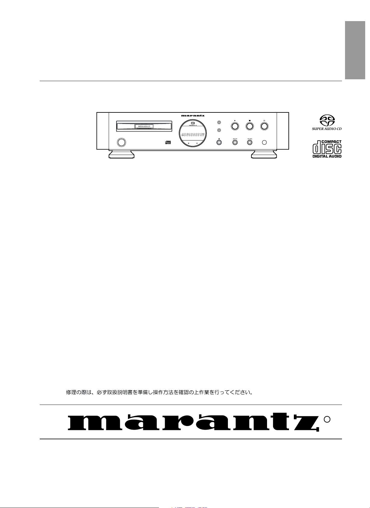
Super Audio CD Player
SUPER AUDIO CD PLAYER SA-14
REP 1
TRACK
RND
PROGRAM TOTAL
POWER
PLAY
SACD CD
OPEN/CLOSE
PLAY
SACD/CD
DISPLAY
TABLE OF CONTENTS
......................................................................................................... 1.7 ELECTRICAL ADJUSTMENTS
............................................................................................... 1.9 EXPLODED VIEW AND PARTS LIST
PAUSESTOP
1-23
1-24
1-26
2. CDM-15M ( SACD MODULE )
2.1 REMOVING AND REINSTALLING THE MAIN PARTS ...................................................................... 2-2
2.2 BLOCK DIAGRAM ............................................................................................................................... 2-5
2.3 SCHEMATIC DIAGRAM ...................................................................................................................... 2-9
2.4 PARTS LOCATION ........................................................................................................................... 2-13
2.5 IC DATA ............................................................................................................................................ 2-17
2.3 EXPLODED VIEW AND PARTS LIST ............................................................................................... 2-36
2.4 ELECTRICAL PARTS LIST ............................................................................................................... 2-37
Please use this service manual with referring to the user guide ( D.F.U. ) without fail.
SA-14
R
Printed in Japan
410K855010 KKI
First Issue
2001. 03
Page 2
MARANTZ DESIGN AND SERVICE
MARANTZ AMERICA, INC.
Using superior design and selected high grade components, MARANTZ company has created the ultimate in stereo sound.
Only original
MARANTZ parts can insure that your MARANTZ product will continue to perform to the specifications for which
it is famous.
Parts for your
MARANTZ equipment are generally available to our National Marantz Subsidiary or Agent.
ORDERING PARTS :
Parts can be ordered either by mail or by Fax.. In both cases, the correct part number has to be specified.
The following information must be supplied to eliminate delays in processing your order :
1. Complete address
2. Complete part numbers and quantities required
3. Description of parts
4. Model number for which part is required
5. Way of shipment
6. Signature : any order form or Fax. must be signed, otherwise such part order will be considered as null and void.
USA
MARANTZ AMERICA, INC
440 MEDINAH ROAD
ROSELLE, ILLINOIS 60172
USA
PHONE : 630 - 307 - 3100
FAX : 630 - 307 - 2687
AMERICAS
SUPERSCOPE TECHNOLOGIES, INC.
MARANTZ PROFESSIONAL PRODUCTS
2640 WHITE OAK CIRCLE, SUITE A
AURORA, ILLINOIS 60504 USA
PHONE : 630 - 820 - 4800
FAX : 630 - 820 - 8103
AUSTRALIA
QualiFi Pty Ltd,
24 LIONEL ROAD,
MT. WAVERLEY VIC 3149
AUSTRALIA
PHONE : +61 - (0)3 - 9543 - 1522
FAX : +61 - (0)3 - 9543 - 3677
NEW ZEALAND
WILDASH AUDIO SYSTEMS NZ
14 MALVERN ROAD MT ALBERT
AUCKLAND NEW ZEALAND
PHONE : +64 - 9 - 8451958
FAX : +64 - 9 - 8463554
EUROPE / TRADING
MARANTZ EUROPE B.V.
P.O.BOX 80002, BUILDING SFF2
5600 JB EINDHOVEN
THE NETHERLANDS
PHONE : +31 - 40 - 2732241
FAX : +31 - 40 - 2735578
AUSTRALIA
TECHNICAL AUDIO GROUP PTY, LTD
558 DARLING STREET,
BALMAIN, NSW 2041,
AUSTRALIA
PHONE : 61 - 2 - 9810 - 5300
FAX : 61 - 2 - 9810 - 5355
THAILAND
MRZ STANDARD CO.,LTD
746 - 754 MAHACHAI ROAD.,
WANGBURAPAPIROM, PHRANAKORN,
BANGKOK, 10200 THAILAND
PHONE : +66 - 2 - 222 9181
FAX : +66 - 2 - 224 6795
TAIWAN
PAI- YUING CO., LTD.
6 TH FL NO, 148 SUNG KIANG ROAD,
TAIPEI, 10429, TAIWAN R.O.C.
PHONE : +886 - 2 - 25221304
FAX : +886 - 2 - 25630415
BRAZIL
PHILIPS DA AMAZONIA IND. ELET. ITDA
CENTRO DE INFORMACOES AO
CEP 04698-970
SAO PAULO, SP, BRAZIL
PHONE : 0800 - 123123
FAX : +55 11 534. 8988
(Discagem Direta Gratuita)
CANADA
LENBROOK INDUSTRIES LIMITED
633 GRANITE COURT,
PICKERING, ONTARIO L1W 3K1
CANADA
PHONE : 905 - 831 - 6333
FAX : 905 - 831 - 6936
SINGAPORE
WO KEE HONG DISTRIBUTION PTE LTD
130 JOO SENG ROAD
#03-02 OLIVINE BUILDING
SINGAPORE 368357
PHONE : +65 858 5535 / +65 381 8621
FAX : +65 858 6078
MALAYSIA
WO KEE HONG ELECTRONICS SDN. BHD.
SUITE 8.1, LEVEL 8, MENARA GENESIS,
NO. 33, JALAN SULTAN ISMAIL,
50250 KUALA LUMPUR, MALAYSIA
PHONE : +60 3 - 2457677
FAX : +60 3 - 2458180
JAPAN
MARANTZ JAPAN, INC.
35- 1, 7- CHOME, SAGAMIONO
SAGAMIHARA - SHI, KANAGAWA
JAPAN 228-8505
PHONE : +81 42 748 1013
FAX : +81 42 741 9190
Technical
KOREA
MK ENTERPRISES LTD.
ROOM 604/605, ELECTRO-OFFICETEL, 16-58,
3GA, HANGANG-RO, YONGSAN-KU, SEOUL
KOREA
PHONE : +822 - 3232 - 155
FAX : +822 - 3232 - 154
SHOCK, FIRE HAZARD SERVICE TEST :
CAUTION : After servicing this appliance and prior to returning to customer, measure the resistance between either primary AC
cord connector pins ( with unit NOT connected to AC mains and its Power switch ON ), and the face or Front Panel of product and
controls and chassis bottom.
Any resistance measurement less than 1 Megohms should cause unit to be repaired or corrected before AC power is applied, and
verified before it is return to the user/customer.
Ref. UL Standard No. 1492.
In case of difficulties, do not hesitate to contact the Technical
Department at above mentioned address.
001120KKI
Page 3

1.1 TECHNICAL SPECIFICATIONS
Audio Characteristics
Channels 2channels 2channels
Frequency range 2 Hz - 100 kHz 2 Hz - 20 kHz
Frequency characteristics 2 Hz - 50 kHz (-3 dB) 2 Hz - 20 kHz
Dynamic range 113 dB 100 dB
THD (1 kHz) 0.0015 % 0.0020 %
wow & flutter Precision of quartz Precision of quartz
Analog output
output level (unbalanced) 2.2 V 2.2 V
output level (balanced) 4.3 V 4.3 V
Digital output
output level (cinch JACK) - 0 .5 Vp-p (75 ohm)
output level (optical) - -19 dBm
Optical Readout System
Laser AlGaAs AlGaAs
Wave length 650 nm 780 nm
Super Audio CD CD
Sampling frequency 2.8224 MHz 44.1 kHz
Power Supply
/F1N version ................................................................................................ AC 100 V 50Hz/60 Hz
/U1G, U1B version ................................................................................................ AC 120 V 60 Hz
/N1G, /S1G version ................................................................................................ AC 230 V 60 Hz
/C1G version ................................................................................................ AC 220 V 60 Hz
Power Consumption ...................................................................................................................... 21 W
Cabinet, etc.
Dimensions (Width x Height x Depth) ................................................................... 458 x110 x 392 mm
Net weight ................................................................................................................................. 11.8 kg
Operating temperatures ................................................................................................+5 ˚C ~ +35 ˚C
Operating humidity ....................................................................................... 5 % ~ 90 % (without dew)
Accessories
Remote control unit (RC-14SA) .......................................................................................................... 1
Dimensions (Width x Height x Depth) ............................................................... 44 x 17.5 x 239 mm
Net weight (without Batteries) .................................................................................................. 175 g
AAA (R03) Batteries ............................................................................................................................ 2
Stereo audio cable with cinch pins ...................................................................................................... 1
AC Power Cord ................................................................................................................................... 1
User’s Guide ....................................................................................................................................... 1
Specifications subject to change without prior notice.
1-1
Page 4

1.2. TEST MODE
1. How to enter the initial test mode
Turn the power on, press the SACD/CD button and the
track down button more than two seconds.
Display: F 0 TEST
2. Version check mode
1 Press the SACD/CD button to enter this mode.
Display: 1 0
2 Model number (Press the PLAY button in the step 1 .)
Display: 1 0 0 0 0 1 0
3 Version (Press the PLAY button in the step 2 .)
Display: 1 0 A 0 0 0 1
4 Then press the PLAY button to return to the initial test
mode.
Display: F 0 TEST
3. Laser test mode
1 Press the PAUSE button to enter this mode.
(In case of the no disc mode, eject the tray.)
Display: 3 0 0 0 0 0 0
2 Enter the laser test mode.
Display: 3 1 0 0 0 0 0
3 CD laser lit up (Press the STOP button in the step 2 or
4.)
Display: 3 1 0 0 0 0 0
4 SACD laser lit up (Press the PAUSE button in the step 2
or 3.)
Display: 3 1 0 0 0 0 0
5 Laser test mode completed (Press the PLAY button in
the step 2, 3 or 4.)
Display: F 0 TEST
9 0 9 2 8
Year/Month/Day
Model number
Version number
4. FIP test
1 Press the PLAY button to enter this mode
Display: All lamps lit up.
2 Press the PLAY button again to return to the initial test
mode
Display: F 0 TEST
5. How to exit the test mode
In case of finish the test mode, press the mains switch
(POWER button)
1-2
Page 5
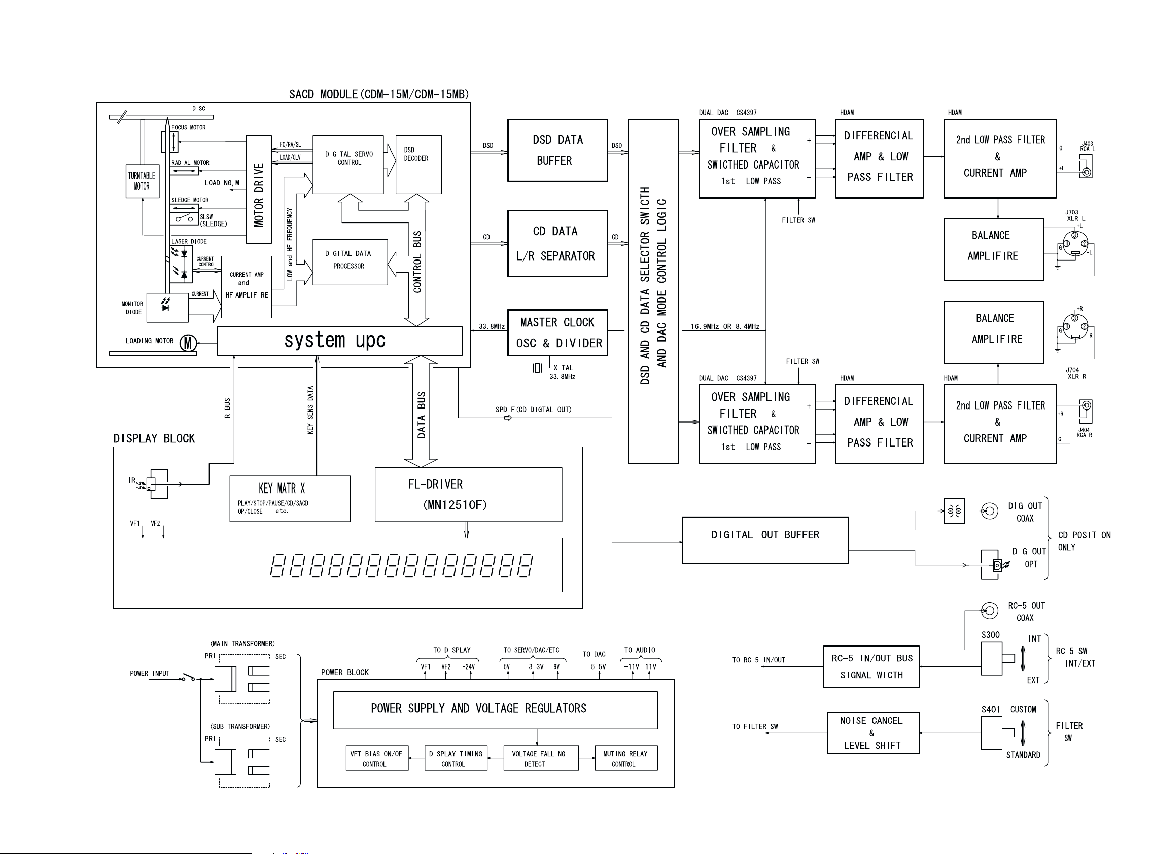
1.3 BLOCK DIAGRAM
1-3 1-4
Page 6
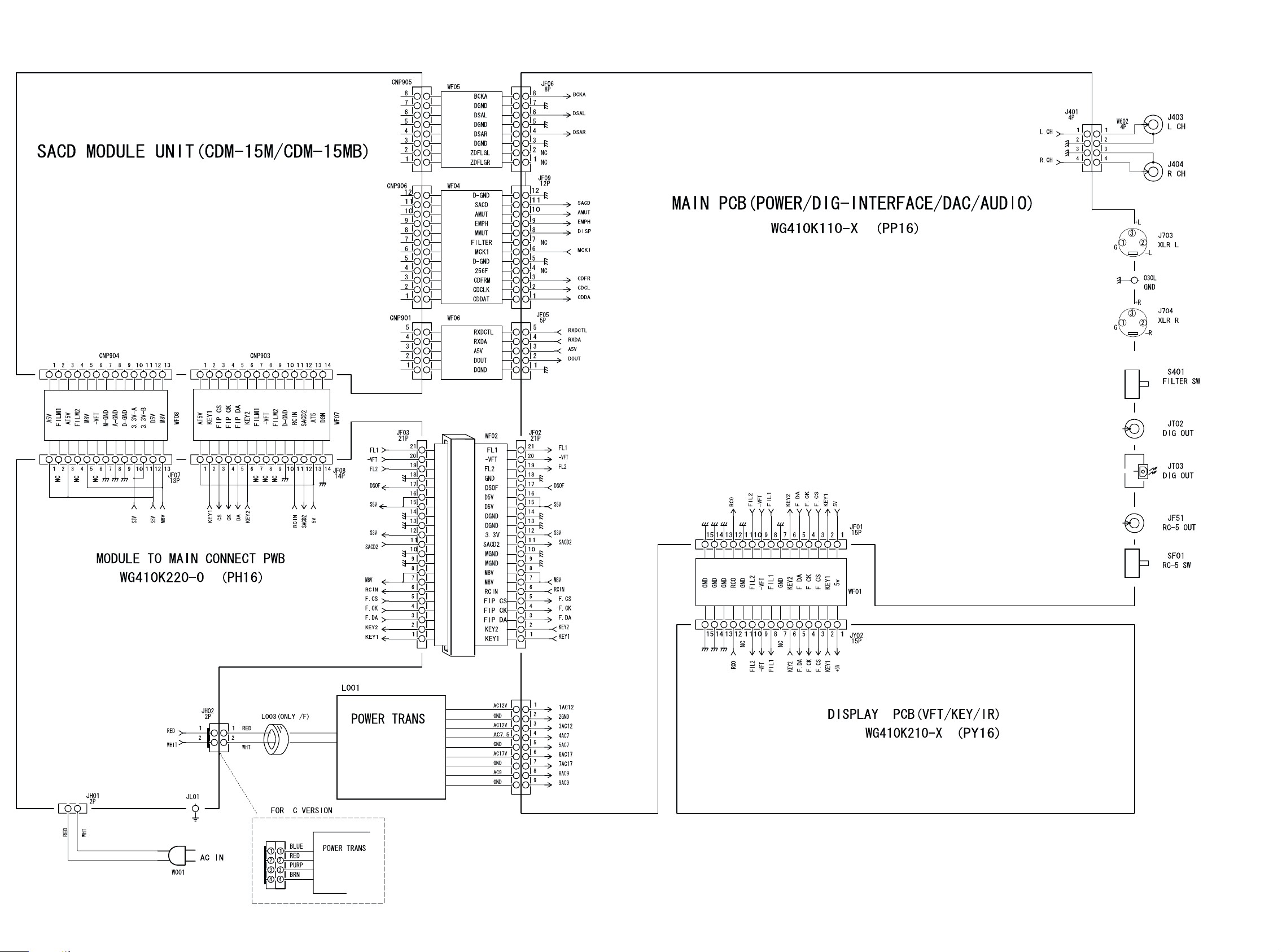
1.4 WIRING DIAGRAM
1-5 1-6
Page 7
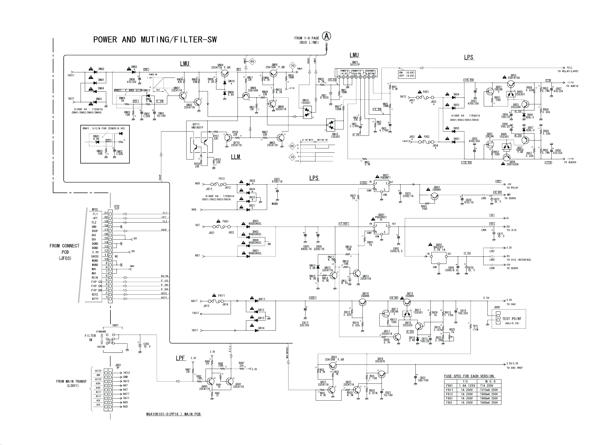
1.5 SCHEMATIC DIAGRAM
1-7 1-8
Page 8
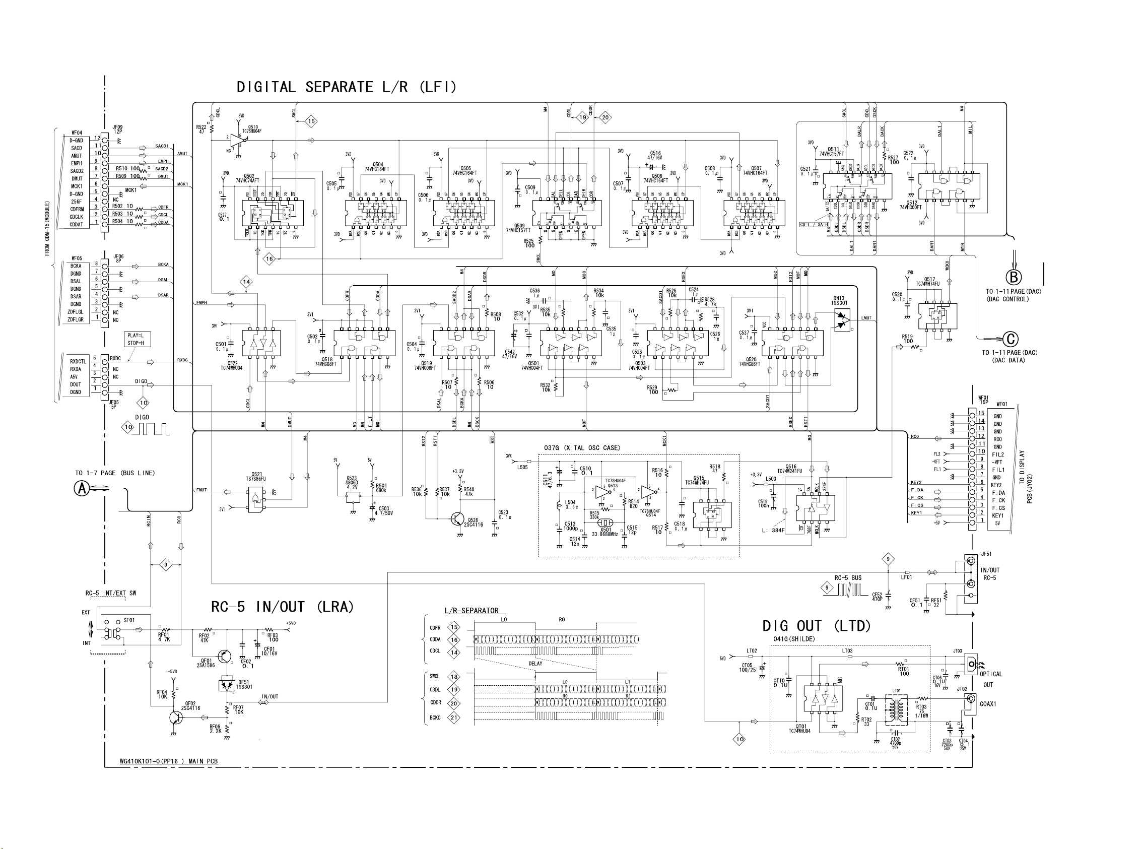
1-9 1-10
Page 9
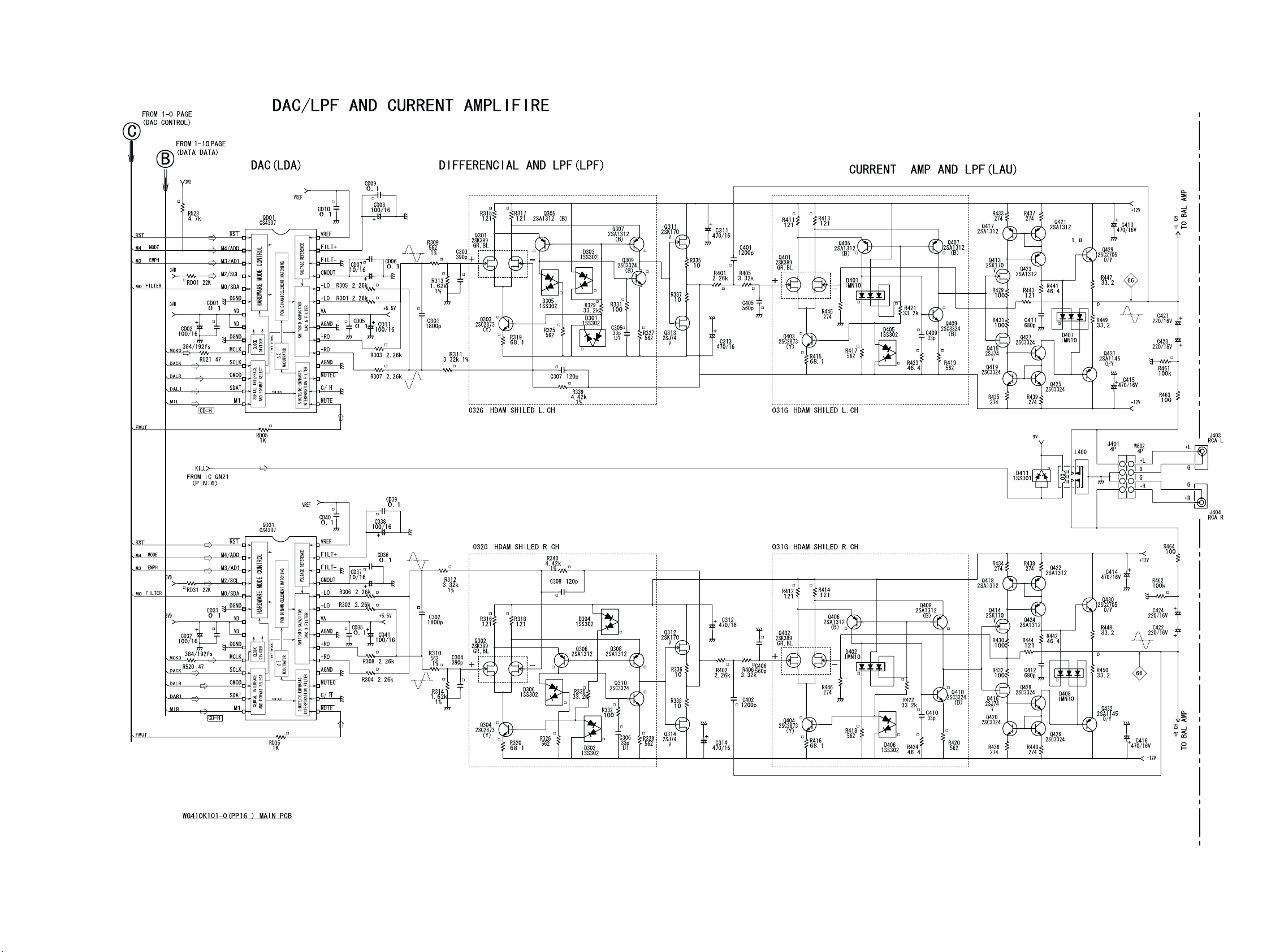
1-11 1-12
Page 10
REP 1
RND
TRACK
PROGRAM TOTAL
PLAY
1-13 1-14
SACD
CD
Page 11
1-15 1-16
Page 12
1-17 1-18
Page 13
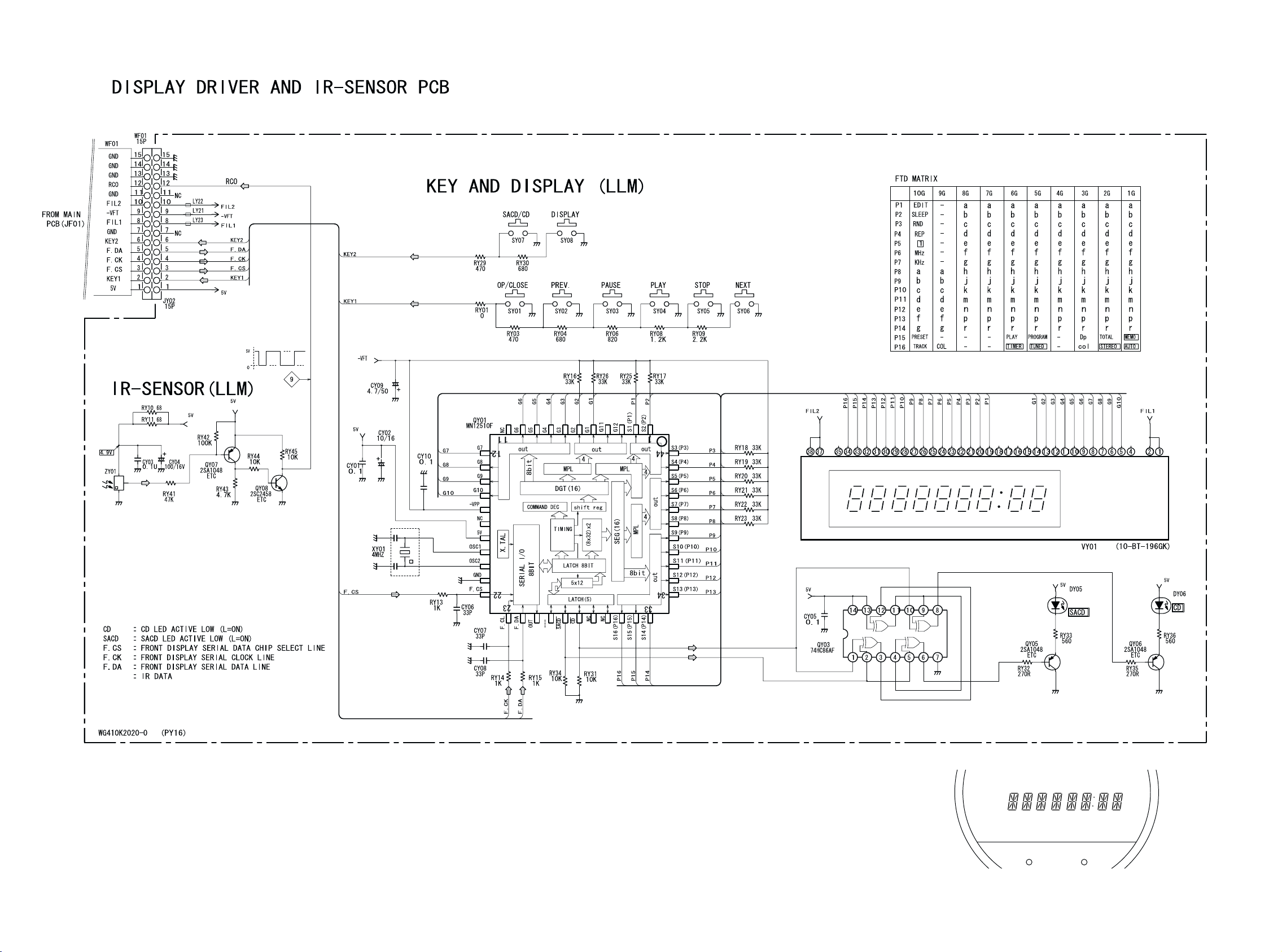
1.6 PARTS LOCATION
QN58
QN56
QN57
QN55
Q716 Q712
Q718 Q714
Q702
Q708 Q704
Q710 Q706
Q715 Q711
Q717 Q713
Q701
Q707 Q703
Q709 Q705
Q432 Q416
Q426 Q420
Q428 Q424
Q418 Q422
Q430 Q414
Q431 Q415
Q425 Q419
Q427 Q423
Q417 Q421
Q429 Q413
Q410 Q406
Q408 Q404
Q402
Q409 Q405
Q407 Q403
Q401
Q314
Q312
Q313
Q311
Q310 Q308 Q304
Q302
Q305 Q303
Q309 Q307 Q301
QD24 - QD21 Q507
QD31 Q506
Q509
Q512 Q505
Q504
Q511 Q502
QD01 Q517 Q510 Q526
QF01 QT01
QF02
Q856 Q857 Q853 Q852
Q855 Q851 QN21
QN12 QN13 Q810 Q811 Q817 Q815 Q813
Q821 Q801
QN04 QN05 Q492 Q491
QY10 QN06
QY11 QN03
QN09
QN01 QN02
1-19 1-20
Q516
Q515
Q514 Q513
Q501
Q520
Q503
Page 14
PH16
QY61 QY12
PY16
QY05 QY03
QY06
QY01 QY08
1-21 1-22
QY07
Page 15

1.7 ELECTRICAL ADJUSTMENTS
. Adjustment the Voltage of DAC (CS4397)
.Purpose
Set the Voltage of Audio part CS4397(QD01, QD31).
Adjustment point : R825(2.2Kohm)
Test point : J800
Equipment : Digital Multi Meter(DC voltage)
.Adjust the voltage at that status 5.4V to 5.5V by the trim
resister R825.
.If there incorrect adjust, the unit shouls be defective of
DISTORTION and AUDIO OUT PUT Voltage.
QD01/QD31(CS4397)
Fig-1 and Fig-2 chart are condition for DAC and pin of IC.
Select the CD/SACD mode by Fig-1 and Fig-2
Note
1. Set the CMOD of SACD(12pin=H)
2. When replay CD disc, A frequency of 44.1KHz input CMOD
3. The master CLK(192/384fs) for MCLK change by mode.
1-23
Page 16

1.8 IC DATA
QD01/QD31 CS4397
Block Diagram
SCLK
LRCK
SDATA
SERIAL INTERFACE
AND FORMAT SELECT
SOFT MUTE
DE-EMPHASIS
FILTER
Pin Configuration
MCLK
3.3 V
Digital
CLOCK
DIVIDER
M3 M2
M4
(AD0/CS)
(AD1/CDIN) (SCL/CCLK)
+
Mode
Select
(Control Po rt)
Audio
Data
Processor
External Clock
INTERPOLATION
FILTER
INTERPOLATION
FILTER
HARDWARE MODE CONTROL
(CONTROL POR T)
M0
M1
(SDA/CDOUT)
7
VD
5
M0 (SDA/CDOUT)
14
M1 (GND)
4
M2 (SCL/CCLK)
3
M3 (AD1/CDIN)
2
M4 (AD0/CS)
16
C/H
12
LRCK
11
SCLK
13
SDATA
15
MUTE
1
RST
10
MCLK
VD
CS4397
DGND
6
MULTI-BIT
DS
MODULATOR
MULTI-BIT
DS
MODULATOR
RESET MUTEC MUTE
8
22
VREF
FILT+
FILT-
CMOUT
AOUTL-
AOUTL+
MUTEC
AOUTR-
AOUTR+
AGND
21
VA
189
DYNAMIC
ELEMEN T
MATCHING
LOGIC
DYNAMIC
ELEMEN T
MATCHING
LOGIC
28
27
26
25
24
23
17
19
20
SWITCHED
CAPACITOR-DAC
AND FILTER
SWITCHED
CAPACITOR-DAC
AND FILTER
VOLTAGE REFERENCE
VREF CMOUTFILT-
FILT+
+
Analog
Conditioning
Analog
Conditioning
+5.5V
Analog
+
+
AOUTL+
AOUTL-
AOUTR+
AOUTR-
+5.5/3.5V
Analog
Q801
PQ05RD21
PQ15RW11
&
PQ09RF1
Q821
Pin Configuration
23
4
1
1 DC input(Vin)
2 DC output(Vo)
3 GND
4 Output voltage adjustment
terminal(Vadj)
1-24
1
Input
Block Diagram
Specific IC
3
GND
2
Output
4
Output voltage
adjustment terminal
Page 17

TA7317P(QN21)
CS4397
Pin Function
No. Pin Name I/O Description
1 RST I Reset input (Low active)
2 M4(AD0/CS) I See Fig-1
3 M3(AD1/CDIN) I See Fig-1
4 M2(SCL/CCLK)) I See Fig-1
5 M0(SDA/CDOUT) I/O See Fig-1
6 DGND Digital ground
7 VD Digital power supply +3.3V
8 VD Digital power supply +3.3V
9 DGND Digital ground
10 MCLK I Master clock
PCM mode:384Fs(16.9344MHz)
DSD mode:192Fs (8.4672MHz/16.9344MHz)
11 SCLK I Serial data clock
12 LRCK(PCM) I PCM mode:Left/Right channel clock(44.1KHz)
CLKMODE(DSD) I DSD mode:Select H(3.3V)
13 SDATA(PCM) I PCM mode:Serial audio data
DSD_L(DSD)
14 M1(PCM) I PCM mode:(Low)
DSD_R(DSD) DSD mode:Direct Stream Digital audio data (Right)
15 MUTE I Mute input (Low active)
16 C/H I Control port (H) /Hardware (L) mode select
17 MUTEC O Mute control (Low active)
18 AGND Analog ground
19 AOUTR- O Right channel negative Analog out
20 AOUTR+ O Right channel positive Analog out
21 AND Analog ground
22 VA Analog power supply +5.5V
23 AOUTL+ O Left channel positive Analog out
24 AOUTL- O Left channel negative Analog out
25 CMOUT O Common mode voltage
26 FILT- I Reference ground
27 FILT+ O Reference filter
28 VREF Voltage reference input
DSD mode:Direct Stream Digital audio data (Left)
1-25
Page 18

1.9 EXPLODED VIEW AND PARTS LIST
VERS.
POS.
COLOR
NO
001B /C1G
/S1G
/U1G
001B /F1N FRONT PANEL ASSY GOLD
001B /U1B FRONT PANEL ASSY BLACK
002B /C1G
/S1G
/U1G
002B /F1N FRONT PANEL GOLD
002B /U1B FRONT PANEL BLACK 410K248010
003B /C1G
/S1G
/U1G
003B /F1N 4822 426 10497 ESCUTCHEON GOLD 269J063110
003B /U1B 4822 426 10496 ESCUTCHEON BLACK 269J063010
005B GOLD 4822 381 12016 LENS IR GOLD 256J355030
005B BLACK 4822 381 12015 LENS IR BLACK 256J355040
006B GOLD RING GOLD NO.4 410K353120
006B BLACK RING BLACK NO.1 410K353010
007B SPRING FOR RING 410K115010
008B GOLD 9965 000 01554 BADGE MNTZ GOLD 313J251110
008B BLACK 9965 000 01553 BADGE MNTZ BLACK 313J251010
009B WINDOW 410K158010
010B GOLD BUSHING POWER/TRAY
010B BLACK BUSHING POWER/TRAY
012B GOLD BUSHING FL/PLAY BUTTON
012B BLACK BUSHING FL/PLAY BUTTON
014B INDICATOR SACD LOGO 410K265010
015B INDICATOR SACD/CD LENS 410K265020
016B LENS SACD/CD 392K355020
018B GOLD BUTTON POWER GOLD 410K270110
018B BLACK BUTTON POWER BLACK 410K270010
019B GOLD BUTTON PLAY/STOP GOLD 410K270120
019B BLACK BUTTON PLAY/STOP BLACK 410K270020
021B GOLD BUTTON OPEN/CLOSE GOLD 410K270130
021B BLACK BUTTON OPEN/CLOSE
028B BADGE SACD LOGO 410K251010
001D GOLD LID TOP GOLD 410K257110
001D BLACK LID TOP BLACK 410K257010
002D SHEET FOR TOP LID INSIDE 313J107010
005D GOLD 4822 502 14425 SCREW FOR TOP LID 323S010020
005D BLACK 4822 502 21693 SCREW FOR TOP LID 323S010030
006D GOLD 4822 426 10499 SIDE PANEL GOLD 269J249110
006D BLACK 4822 426 10498 SIDE PANEL BLACK 269J249010
009D GOLD 4822 502 14425 SCREW FOR SIDE PANEL 323S010020
009D BLACK 4822 502 21693 SCREW FOR SIDE PANEL 323S010030
PART NO.
(PCS)
4822 426 10497 ESCUTCHEON GOLD 269J063110
DESCRIPTION
ASSY GOLD BLAST 410K248520
AIR
LAST
FRONT PANEL GOLD BLAST 410K248110
HAIR LINE
GOLD
BLACK
GOLD
BLACK
BLACK
PART NO.
(MJI)
410K248530
410K248510
410K248120
410K259110
410K259010
410K259120
410K259020
410K270030
VERS.
POS.
COLOR
NO
A001 GOLD MECHANISM SACD CDM-15M 392K304510
A001 BLACK MECHANISM SACD
L001 /C1 MAINS TRANSF. 110/220V TS46010040
L001 /F1 MAINS TRANSF. 100V TS46010010
L001 /S1 MAINS TRANSF.MAIN 230V TS46010020
L001 /U1 MAINS TRANSF.MAIN 120V TS46010030
W001 /C1G MAINS CORD CORDSET
W001 /F1N 4822 321 11337 MAINS CORD MITY
W001 /S1G MAINS CORD S PORE
W001 /U1B MAINS CORD UL/CSA
W001 /U1G MAINS CORD UL/CSA
001T /C1,/S1 USER GUIDE SA-14 410K851350
001T /F1 USER GUIDE SA-14 410K851110
001T /U1 USER GUIDE SA-14 410K851250
T100 UNIT KIT REMOTE
001S PACKING CASE 410K801010
002S CUSHION LEFT 410K809010
003S CUSION RIGHT 410K809020
006S PROTECTOR TRAY
PART NO.
(PCS)
DESCRIPTION
CDM-15MB
7A 250V
3P 12A 125V F
2P 10A 250V
10A 125V
10A 125V
PACKING
CONTROLLER RC-14SA
NOT STANDARD SPARE
PARTS
ESCUTCHEON
PART NO.
(MJI)
392K304520
ZC02009010
ZC01802080
ZC01804100
ZC01803100
ZC01803100
ZK410K0010
392K269010
004G LEG GOLD 163J057410
011G 9965 000 00588 POWER BUTTON LINK 376K121010
012G INSULATOR SHAFT
POWER BUTTON
001M SCREW MECHANISM 410K010010
002M GOLD ESCUTCHEON GOLD 392K063150
002M BLACK ESCUTCHEON BLACK 392K063050
003M ESCUTCHEON SACD LOGO 392K063160
410K120010
1-26
Page 19

1-27
1-28
Page 20

1.10 ELECTRICAL PARTS LIST
ASSIGNMENT OF COMMON PARTS CODES.
RESISTORS
R : 1) GD05 140, Carbon film fixed resistor, 5% 1/4W
R : 2) GD05 160, Carbon film fixed resistor, 5% 1/6W
Examples ;
Resistance value
0.1 001 10 100 1 k 102 100 k 104
0.5 005 18 180 2.7 k 272 680 k 684
1 010 100 101 10 k 103 1 M 105
6.8 068 390 391 22 k 223 4.7 M 475
Note : Please distinguish 1/4W from 1/6W by the shape of par ts
used actually.
CAPACITORS
C : CERAMIC CAP.
3) DD1 370, Ceramic capacitor
Examples ;
Tolerance (Capacity deviation)
±
Tolerance of COMMON PARTS handled here are as follows :
C : CERAMIC CAP.
Examples ;
C : 5) ELECTROLY CAP. ( ), 6) FILM CAP. ( )
Examples ;
Examples ;
NOTE
0.5 pF 5 pF .... 0.25 pF
Capacity value
0.5 pF .... 005 3 pF .... 030 100 pF .... 101
1.5 pF .... 015 47 pF .... 470 560 pF .... 561
4) DK16 300, High dielectric constant ceramic
Capacity value
100 pF .... 101 1000 pF .... 102 10000 pF .... 103
470 pF .... 471 2200 pF .... 222
5) EA
Capacity value
0.1 µF ....104 4.7 µF ....475 100 µF ....107
0.33 µF ....334 10 µF ....106 330 µF ....337
Working voltage
6) DF15 350 Plastic film capacitor
DF15 310 One-way type, Mylar 5% 50V
DF16 310 Plastic film capacitor
Capacity value
0.001 µF (1000 pF) ....... 102 0.1 µF .... 104
0.0018 µF ........................ 182 0.56 µF....564
0.01 µF ........................ 103 1 µF .... 105
0.015 µF ........................ 153
: 1) The above CODES ( R , R , C , C and
C ) are omitted on the schematic diagram in some
2) On the occasion, be confirmed the common parts on
3) Refer to “Common Parts List” for the other common
{
Resistance value
{
0.25 pF .... 0
±
0.5 pF .... 1
±5% .... 5
6 pF 10 pF .... 0.5 pF
12 pF 560 pF .... 5%
1 pF .... 010 10 pF .... 100 220 pF .... 221
{
{
1 µF....105 22 µF .... 226 1100 µF ....118
6.3V ....006 25V ....025
10V ....010 35V .... 035
16V ....016 50V .... 050
{
case.
the parts list.
parts (RI05, DD4, DK4).
Disc type
Temp.coeff.P350 N1000, 50V
Capacity value
Tolerance
±
±
±
capacitor
Disc type
Temp.chara. 2B4, 50V
Capacity value
10, Electrolytic capacitor
{
One-way lead type, Tolerance 20%
Working voltage
Capacity value
2200 µF ....228
One-way type, Mylar 10% 50V
Capacity value
±
±
NOTE ON SAFETY FOR FUSIBLE RESISTOR :
The suppliers and their type numbers of fusible resistors
are as follows;
1. KOA Corporation
Part No. (MJI) Type No. (KOA) Description
NH05 140 RF25S J ( 5% 1/4W)
NH05 120 RF50S J ( 5% 1/2W)
NH85 110 RF73B2A J ( 5% 1/10W)
NH95 140 RF73B2E J ( 5% 1/4W)
2. Matsushita Electronic Components Co., Ltd
Part No. (MJI) Type No. (MEC) Description
NF05 140 ERD-2FCJ ( 5% 1/4W)
RF05 140
NF02 140
RF02 140
Examples ;
{
Resistance value
ERD-2FCG
{
Resistance value
Resistance value
0.1 001 10 100 1 k 102 100 k 104
0.5 005 18 180 2.7 k 272 680 k 684
1 010 100 101 10 k 103 1 M 105
6.8 068 390 391 22 k 223 4.7 M 475
{
( 2% 1/4W)
±
±
±
±
Resistance value
(0.1 10 k )
±
±
{
Resistance value
ABBREVIATION AND MARKS
ANT. : ANTENNA BATT. : BATTERY
CAP. : CAPACITOR CER. : CERAMIC
CONN. : CONNECTING DIG. : DIGITAL
HP : HEADPHONE MIC. : MICROPHONE
µ-PRO : MICROPROCESSOR REC. : RECORDING
RES. : RESISTOR SPK : SPEAKER
SW : SWITCH TRANSF. : TRANSFORMER
TRIM. : TRIMMING TRS. : TRAMSISTOR
VAR. : VARIABLE X’TAL : CRYSTAL
±
NOTE ON SAFETY :
Symbol Fire or electrical shock hazard. Only original
parts should be used to replaced any part marked with
symbol
than original type), may increase risk of fire or electrical
shock hazard.
. Any other component substitution (other
VERS.
POS.
COLOR
NO
CF24 4822 124 90364 ELECT 220
CF26 4822 124 90364 ELECT 220
CY60 4822 122 40588 CER. 0.022
CY61 4822 122 40588 CER. 0.022
CY62 4822 124 90355 ELECT 100
CY63 4822 124 41536 ELECT 100
R
DF01
DF10
DY01 4822 130 82421 DIODE 1D3 1A/200V HD20002710
DY02 4822 130 82421 DIODE 1D3 1A/200V HD20002710
DY61
DY64
DY65 4822 130 80116 ZENER DIODE 24V HD32401000
DY66 4822 130 32362 DIODE 1SS176 MA165 1SS254
QY12 4822 130 60839 TRS. 2SC2458 (Y GR) HT324582B0
QY61 4822 130 42715 TRS. 2SA1048 2SA933S
FH01 /C1,/S1,
/U1
GH01 4822 121 43732 FILM 0.01 F M 250V AC DF77103500
JF03 JACK 21FE-ST-VK-N YJ07020170
JH01 JACK MAINS INLET M1818-A YJ04002510
L002 /C1,/S1 4822 146 10891 MAINS TRANSF. SUB 115/230V TS13517060
L002 /F1 MAINS TRANSF.SUB 100V TS13517050
L002 /U1 MAINS TRANSF.SUB 120V TS13517070
SH01 4822 276 13364 PUSH SWITCH SDDLD1
CD01 4822 126 11687 CER. 0.1
CD02 4822 124 90354 ELECT 100
CD05 4822 126 11687 CER. 0.1
CD06 4822 126 11687 CER. 0.1
CD07 4822 124 22237 ELECT 10
CD08 4822 124 23514 ELECT 100
CD09 4822 126 11687 CER. 0.1
CD10 4822 126 11687 CER. 0.1
CD11 4822 124 23514 ELECT 100
CD21 4822 124 90352 ELECT 10
CD22 4822 124 90353 ELECT 100
CD31 4822 126 11687 CER. 0.1
CD32 4822 124 90354 ELECT 100
CD35 4822 126 11687 CER. 0.1
CD36 4822 126 11687 CER. 0.1
CD37 4822 124 22237 ELECT 10
CD38 4822 124 23514 ELECT 100
CD39 4822 126 11687 CER. 0.1
CD40 4822 126 11687 CER. 0.1
CD41 4822 124 23514 ELECT 100
PART NO.
(PCS)
4822 130 32362 DIODE 1SS176 MA165 1SS254
4822 130 82421 DIODE 1D3 1A/200V HD20002710
4822 252 11189 FUSE T2.5A/250V TR5 N
DESCRIPTION
PH16-POWER SW/SUB TRANS
CIRCUIT BOARD
PH16-CAPACITORS
F M 16V OA22701620
F M 16V OA22701620
F 20% DA17223110
F 20% DA17223110
F M 50V OA10705020
F M 35V OA10703520
PH16-RESISTORS(COMMON)
CARBON FILM FIXED RES.
5% 1/6W : RY55-RY58 RY61
PH16-SEMICONDUCTORS
30V 0.1A
30V 0.1A
2SA1267
PH16-MISCELLANEOUS
O.19372
POWER TV-3
PP16-MAIN/DAC/AUDIO
CIRCUIT BOARD
PP16-CAPACITORS
F +80% -20% 25V DK98104200
F M 16V OA10701620
F +80% -20% 25V DK98104200
F +80% -20% 25V DK98104200
F 16V OA10601650
F 16V OA10701650
F +80% -20% 25V DK98104200
F +80% -20% 25V DK98104200
F 16V OA10701650
F M 16V OA10601620
F M 10V OA10701020
F +80% -20% 25V DK98104200
F M 16V OA10701620
F +80% -20% 25V DK98104200
F +80% -20% 25V DK98104200
F 16V OA10601650
F 16V OA10701650
F +80% -20% 25V DK98104200
F +80% -20% 25V DK98104200
F 16V OA10701650
PART NO.
(MJI)
HD20002000
HD20002000
HT10001000
FS20250200
SP01011990
VERS.
POS.
COLOR
NO
CF01 4822 124 90352 ELECT 10 F M 16V OA10601620
CF02 4822 126 11687 CER. 0.1
CF51 4822 126 11687 CER. 0.1
CF52 4822 126 11568 CER. 470pF
CN02 4822 124 41543 ELECT 1
CN03 4822 124 90352 ELECT 10
CN06 4822 124 41541 ELECT 470
CN13 4822 126 11687 CER. 0.1
CN21 4822 126 11567 CER. 0.022
CN22 4822 124 90357 ELECT 2.2
CN23 4822 124 22274 ELECT 4.7
CT01 4822 126 11687 CER. 0.1
CT02 4822 126 11685 CER. 4700 pF
CT03 4822 126 12339 CER. 2200pF
CT04 4822 126 11687 CER. 0.1
CT05 4822 124 80119 ELECT 100
CT06 4822 126 11687 CER. 0.1
CT10 4822 126 11687 CER. 0.1
C301 FILM 1800pF
C302 FILM 1800pF
C303 MICA CHIP 390pF
C304 MICA CHIP 390pF
C305 4822 123 30422 MICA CHIP 33pF 500WV DF95330500
C306 4822 123 30422 MICA CHIP 33pF 500WV DF95330500
C307 MICA CHIP 120pF 500WV DF95121500
C308 MICA CHIP 120pF 500WV DF95121500
C311 /C1,/S1 4822 124 80958 ELECT 470
C311 /F1,/U1 4822 124 11953 ELECT 470
C312 /C1,/S1 4822 124 80958 ELECT 470
C312 /F1,/U1 4822 124 11953 ELECT 470
C313 /C1,/S1 4822 124 80958 ELECT 470
C313 /F1,/U1 4822 124 11953 ELECT 470
C314 /C1,/S1 4822 124 80958 ELECT 470
C314 /F1,/U1 4822 124 11953 ELECT 470
C355 4822 126 11687 CER. 0.1
C401 MICA CHIP 1200pF 100WV DF95122510
C402 MICA CHIP 1200pF 100WV DF95122510
C405 4822 123 30362 MICA CHIP 560pF 100WV DF95561510
C406 4822 123 30362 MICA CHIP 560pF 100WV DF95561510
C409 4822 123 30422 MICA CHIP 33pF 500WV DF95330500
C410 4822 123 30422 MICA CHIP 33pF 500WV DF95330500
C411 9965 000 01564 FILM 680pF
C412 9965 000 01564 FILM 680pF
C413 /C1,/S1 4822 124 80958 ELECT 470
C413 /F1,/U1 4822 124 11953 ELECT 470
C414 /C1,/S1 4822 124 80958 ELECT 470
C414 /F1,/U1 4822 124 11953 ELECT 470
C415 /C1,/S1 4822 124 80958 ELECT 470
C415 /F1,/U1 4822 124 11953 ELECT 470
C416 /C1,/S1 4822 124 80958 ELECT 470
C416 /F1,/U1 4822 124 11953 ELECT 470
C421
C424
C501 4822 126 11687 CER. 0.1
C502 4822 126 11687 CER. 0.1
C503 4822 124 22274 ELECT 4.7
C504
C510
C511 4822 124 11131 TANTAL CHIP 47
C513 5322 126 11578 CER. 1000pF
C514 4822 126 11663 CER. 12pF
C515 4822 126 11663 CER. 12pF
PART NO.
(PCS)
4822 124 80123 ELECT 220 F 16V OA22701640
4822 126 11687 CER. 0.1 F +80% -20% 25V DK98104200
DESCRIPTION
F +80% -20% 25V DK98104200
F +80% -20% 25V DK98104200
10% 50V DK96471300
F 50V OA10505020
F M 16V OA10601620
F M 35V OA47703520
F +80% -20% 25V DK98104200
F 10% 25V DK96223200
F M 50V OA22505020
F M 50V OA47505020
F +80% -20% 25V DK98104200
10 % 50V DK96472300
10% 50V DK96222300
F +80% -20% 25V DK98104200
F 25V OA10702540
F +80% -20% 25V DK98104200
F +80% -20% 25V DK98104200
5% 160V OF55182550
5% 160V OF55182550
5% DF95391500
5% DF95391500
F 16V OA47701640
F M 16V OA47701650
F 16V OA47701640
F M 16V OA47701650
F 16V OA47701640
F M 16V OA47701650
F 16V OA47701640
F M 16V OA47701650
F +80% -20% 25V DK98104200
5% 100V OF55681540
5% 100V OF55681540
F 16V OA47701640
F M 16V OA47701650
F 16V OA47701640
F M 16V OA47701650
F 16V OA47701640
F M 16V OA47701650
F 16V OA47701640
F M 16V OA47701650
F +80% -20% 25V DK98104200
F +80% -20% 25V DK98104200
F M 50V OA47505020
F 6.3V EY47600620
10% B 50V DK96102300
5 % 50V DD95120300
5 % 50V DD95120300
PART NO.
(MJI)
1-29 1-30
Page 21

POS.
NO
VERS.
COLOR
PART NO.
(PCS)
DESCRIPTION
PART NO.
(MJI)
POS.
NO
VERS.
COLOR
PART NO.
(PCS)
DESCRIPTION
PART NO.
(MJI)
C516 4822 124 41539 ELECT 47 F M 16V OA47601620
C518
4822 126 11687 CER. 0.1 F +80% -20% 25V DK98104200
C523
C524 4822 126 13303 CER. 1
C526 4822 126 13303 CER. 1
C527 4822 126 11687 CER. 0.1
C528 4822 126 11687 CER. 0.1
C532 4822 126 11687 CER. 0.1
C535 4822 126 13303 CER. 1
C536 4822 126 13303 CER. 1
C537 4822 126 11687 CER. 0.1
C542 4822 124 41539 ELECT 47
C709 /C1,/S1 4822 124 80958 ELECT 470
C709 /F1,/U1 4822 124 11953 ELECT 470
C710 /C1,/S1 4822 124 80958 ELECT 470
C710 /F1,/U1 4822 124 11953 ELECT 470
C711 /C1,/S1 4822 124 80958 ELECT 470
C711 /F1,/U1 4822 124 11953 ELECT 470
C712 /C1,/S1 4822 124 80958 ELECT 470
C712 /F1,/U1 4822 124 11953 ELECT 470
C713
4822 124 90365 ELECT 220 F M 25V OA22702520
C720
C721
/C1,/S1/U14822 126 11759 CER. 100pF
C724
C801 4822 124 22243 ELECT 6800
C802 4822 124 80773 ELECT 3300
C804 4822 124 80773 ELECT 3300µF
C805 4822 124 40723 ELECT 2200
C811 4822 124 90051 ELECT 220
C813 /F1N 4822 124 22238 ELECT 100
C815 4822 124 22238 ELECT 100
C822 4822 124 80582 ELECT 4700
C823 4822 124 40723 ELECT 2200
C824 4822 124 90371 ELECT 470
C851 ELECT 4700
C852 ELECT 4700
C855 /C1,/S1 4822 124 80119 ELECT 100
C855 /F1,/U1 4822 124 22238 ELECT 100
C856 /C1,/S1 4822 124 80119 ELECT 100
C856 /F1,/U1 4822 124 22238 ELECT 100
C857 4822 124 22242 ELECT 470
C858 4822 124 22242 ELECT 470
C870 4822 126 11687 CER. 0.1
C871 4822 126 11687 CER. 0.1
C872 4822 126 11687 CER. 0.1
PP16-RESISTORS
RD01 4822 051 30223 CHIP 22k
RD05 4822 051 30102 CHIP 1k
!RD19 4822 117 10145 FUSIBLE 3.3
RD20 4822 051 30472 CHIP 4.7k
RD21 4822 051 30472 CHIP 4.7k Ω
RD22 4822 051 30472 CHIP 4.7k
RD23 4822 051 30102 CHIP 1k
RD24 1.15k
RD25 3.01k
RD31 4822 051 30223 CHIP 22k
RD35 4822 051 30102 CHIP 1k
RF01 4822 051 30472 CHIP 4.7k
RF02 4822 051 30473 CHIP 47k
RF04 4822 051 30103 CHIP 10k
RF06 4822 051 30222 CHIP 2.2k
RF07 4822 051 30103 CHIP 10k
F +80% -20% 10V DK98105200
F +80% -20% 10V DK98105200
F +80% -20% 25V DK98104200
F +80% -20% 25V DK98104200
F +80% -20% 25V DK98104200
F +80% -20% 10V DK98105200
F +80% -20% 10V DK98105200
F +80% -20% 25V DK98104200
F M 16V OA47601620
F 16V OA47701640
F M 16V OA47701650
F 16V OA47701640
F M 16V OA47701650
F 16V OA47701640
F M 16V OA47701650
F 16V OA47701640
F M 16V OA47701650
5% 50V DD95101300
F 20% 16V OA68801620
F 20% 6.3V OA33800620
20% 6.3V OA33800620
F 16V OA22801620
F M 25V OA22702550
F 20% 25V OA10702550
F 20% 25V OA10702550
F 20% 16V OA47801620
F 16V OA22801620
F 20% 10V OA47701020
F M 35V OB47803520
F M 35V OB47803520
F 25V OA10702540
F 20% 25V OA10702550
F 25V OA10702540
F 20% 25V OA10702550
F M 25V OA47702550
F M 25V OA47702550
F +80% -20% 25V DK98104200
F +80% -20% 25V DK98104200
F +80% -20% 25V DK98104200
5% 1/16W NN05223610
5% 1/16W NN05102610
5% 1/10W NH85033110
5% 1/16W NN05472610
5% 1/16W NN05472610
5% 1/16W NN05472610
5% 1/16W NN05102610
1% 1/4W GM11411510
1% 1/4W GM11430110
5% 1/16W NN05223610
5% 1/16W NN05102610
5% 1/16W NN05472610
5% 1/16W NN05473610
5% 1/16W NN05103610
5% 1/16W NN05222610
5% 1/16W NN05103610
RF51 4822 117 12139 CHIP 22
RN01 /C1,/S1 4822 130 80132 ZENER DIODE 3.9V HD30391000
RN02 4822 117 11977 CHIP 3.9M
RN03 /C1,/S1 4822 116 83819 CHIP 18k
RN03 /F1,/U1 4822 051 30103 CHIP 10k
RN04 4822 051 30473 CHIP 47k
RN05 4822 051 30103 CHIP 10k
RN07 4822 051 30223 CHIP 22k
RN08 4822 051 30472 CHIP 4.7k
RN09 4822 051 30223 CHIP 22k
RN10 4822 051 30472 CHIP 4.7k
RN11 4822 051 30223 CHIP 22k
RN12 4822 051 30223 CHIP 22k
RN14 4822 051 30103 CHIP 10k
RN15 4822 051 30472 CHIP 4.7k
RN16 4822 051 30472 CHIP 4.7k
RN17 4822 051 30472 CHIP 4.7k
RN18 4822 051 30103 CHIP 10k
RN19 4822 051 30104 CHIP 100k
RN20 4822 051 30472 CHIP 4.7k
RN21 4822 051 30104 CHIP 100k
RN22 4822 051 30104 CHIP 100k
RN23 4822 051 30332 CHIP 3.3k
RN24 4822 051 30473 CHIP 47k
RN25 4822 051 30333 CHIP 33k
RN26 4822 051 30104 CHIP 100k
RN27 4822 051 30332 CHIP 3.3k
RN55
4822 111 90906 CHIP 2.2k 5% 1/10W NI05222110
RN62
RY50
4822 051 30223 CHIP 22k 5% 1/ 16W NN05223610
RY54
RT01 4822 051 30101 CHIP 100 5% 1/16W NN05101610
RT02 4822 051 30339 CHIP 33
RT03 4822 051 30759 CHIP 75
R301
2.26k 1% 1/4W GM11422610
R308
R309 562
R310 562
R311 3.32k
R312 3.32k
R313 1.62k
R314 1.62k
R315
R318
R319 68.1
R320 68.1
R325
R328
R329 33.2k
R330 33.2k
R331 100
R332 100
R335
R338
R339 4.42k
R340 4.42k
R401 2.26k
R402 2.26k
5% 1/16W NN05220610
5% 1/16W NN05395610
5% 1/16W NN05183610
5% 1/16W NN05103610
5% 1/16W NN05473610
5% 1/16W NN05103610
5% 1/16W NN05223610
5% 1/16W NN05472610
5% 1/16W NN05223610
5% 1/16W NN05472610
5% 1/16W NN05223610
5% 1/16W NN05223610
5% 1/16W NN05103610
5% 1/16W NN05472610
5% 1/16W NN05472610
5% 1/16W NN05472610
5% 1/16W NN05103610
5% 1/6W NN05104610
5% 1/16W NN05472610
5% 1/16W NN05104610
5% 1/16W NN05104610
5% 1/16W NN05332610
5% 1/16W NN05473610
5% 1/16W NN05333610
5% 1/16W NN05104610
5% 1/16W NN05332610
5% 1/16W NN05330610
5% 1/16W NN05750610
1% 1/4W GM11456200
1% 1/4W GM11456200
1% 1/4W GM11433210
1% 1/4W GM11433210
1% 1/4W GM11416210
1% 1/4W GM11416210
121 1% 1/4W GM11412100
1% 1/4W GM114681G0
1% 1/4W GM114681G0
562 1% 1/4W GM11456200
1% 1/4W GM11433220
1% 1/4W GM11433220
1% 1/4W GM11410000
1% 1/4W GM11410000
10 1% 1/4W GM114100G0
1% 1/4W GM11444210
1% 1/4W GM11444210
1% 1/4W GM11422610
1% 1/4W GM11422610
1-31
Page 22

POS.
NO
VERS.
COLOR
PART NO.
(PCS)
DESCRIPTION
PART NO.
(MJI)
POS.
NO
VERS.
COLOR
PART NO.
(PCS)
DESCRIPTION
PART NO.
(MJI)
R405 3.32k 1% 1/4W GM11433210
R406 3.32k
R411
R414
R415 68.1
R416 68.1
R417
R420
R421 33.2k
R422 33.2k
R423 46.4
R424 46.4
R429
R432
R433
R440
R441 46.4
R442 46.4
R443 121
R444 121
R445 274
R446 274
R447
R450
R461 100k
R462 100k
R463 100
R464 100
R491 4822 051 30223 CHIP 22k
R492 4822 051 30101 CHIP 100
R493 4822 117 12139 CHIP 22
R494 4822 051 30223 CHIP 22k
R495 4822 051 30224 CHIP 220k
R496 4822 051 30102 CHIP 1k
R497 4822 051 30223 CHIP 22k
R501 4822 051 30684 CHIP 680k
R502 4822 051 30109 CHIP 10
R503 4822 051 30109 CHIP 10
R504 4822 051 30109 CHIP 10
R506 4822 051 30109 CHIP 10
R507 4822 051 30109 CHIP 10
R508 4822 051 30109 CHIP 10
R509 4822 051 30101 CHIP 100
R510 4822 051 30101 CHIP 100
R514 4822 117 12968 CHIP 820
R515 4822 051 30334 CHIP 330k
R516 4822 051 30109 CHIP 10
R517 4822 051 30109 CHIP 10
R518 4822 051 30479 CHIP 47
R519 4822 051 30101 CHIP 100
R520 4822 051 30479 CHIP 47
R521 4822 051 30479 CHIP 47
R522 4822 051 30479 CHIP 47
R523 4822 051 30472 CHIP 4.7k
R525 4822 051 30101 CHIP 100
R526 4822 051 30103 CHIP 10k
R527 4822 051 30101 CHIP 100
R528 4822 051 30103 CHIP 10k
R529 4822 051 30101 CHIP 100
R532 4822 051 30101 CHIP 100
R534 4822 051 30472 CHIP 4.7k
R535 4822 051 30103 CHIP 10k
R536 4822 051 30103 CHIP 10k
1% 1/4W GM11433210
121 1% 1/4W GM11412100
1% 1/4W GM114681G0
1% 1/4W GM114681G0
562 1% 1/4W GM11456200
1% 1/4W GM11433220
1% 1/4W GM11433220
1% 1/4W GM114464G0
1% 1/4W GM114464G0
100 1% 1/4W GM11410000
274 1% 1/4W GM11427400
1% 1/4W GM114464G0
1% 1/4W GM114464G0
1% 1/4W GM11412100
1% 1/4W GM11412100
1% 1/4W GM11427400
1% 1/4W GM11427400
33.2 1% 1/4W GM114332G0
1% 1/4W GM11410030
1% 1/4W GM11410030
1% 1/4W GM11410000
1% 1/4W GM11410000
5% 1/16W NN05223610
5% 1/16W NN05101610
5% 1/16W NN05220610
5% 1/16W NN05223610
5% 1/16W NN05224610
5% 1/16W NN05102610
5% 1/16W NN05223610
5% 1/16W NN05684610
5% 1/16W NN05100610
5% 1/16W NN05100610
5% 1/16W NN05100610
5% 1/16W NN05100610
5% 1/16W NN05100610
5% 1/16W NN05100610
5% 1/16W NN05101610
5% 1/16W NN05101610
5% 1/16W NN05821610
5% 1/16W NN05334610
5% 1/16W NN05100610
5% 1/16W NN05100610
5% 1/16W NN05470610
5% 1/16W NN05101610
5% 1/16W NN05470610
5% 1/16W NN05470610
5% 1/16W NN05470610
5% 1/16W NN05472610
5% 1/16W NN05101610
5% 1/16W NN05103610
5% 1/16W NN05101610
5% 1/16W NN05103610
5% 1/16W NN05101610
5% 1/16W NN05101610
5% 1/16W NN05472610
5% 1/16W NN05103610
5% 1/16W NN05103610
R537 4822 051 30103 CHIP 10k
R540 4822 051 30473 CHIP 47k
R701
R704
R705 100
R706 100
R707
6.81k 1% 1/4W GM11468110
R710
R711
R714
R717
R720
R721 100
R722 100
R723
6.81k 1% 1/4W GM11468110
R726
R727
R730
R737 100k
R738 100k
R739
R742
R743 100k
R744 100k
R745
R748
R801 4822 051 30102 CHIP 1k
R811 100
R812 3.32k
R813 1.15k
R814 3.32k
R815 1.47k
R820 4822 051 30272 CHIP 2.7k
R821 4822 051 30102 CHIP 1k
R823 2.26k
R825 4822 100 11758 TRIMMING RH068 1KB 0.3
R828 1k
R851 100
R852 100
R853 2.74k
R854 3.32k
R855 2.74k
R856 3.32k
R857 3.32k
R858 3.32k
PP16-RESISTORS(COMMON)
R
DF51 4822 130 83715 CHIP DIODE 1SS301 DAN202U HZ21005000
DN01
DN05
DN09 4822 130 33948 ZENER DIODE 5.6V HD30561000
DN10 4822 130 32362 DIODE 1SS176 MA165 1SS254
CARBON FILM FIXED RES.
5% 1/6W : RF03
[RN01(/F1,/U1)] RN06 R841
PP16-SEMICONDUCTORS
DIODE 11EQS10 1A 100V HD20055100
30V 0.1A
5% 1/16W NN05103610
5% 1/16W NN05473610
10k 1% 1/4W GM11410020
1% 1/4W GM11410000
1% 1/4W GM11410000
33.2 1% 1/4W GM114332G0
10k 1% 1/4W GM11410020
1% 1/4W GM11410000
1% 1/4W GM11410000
33.2 1% 1/4W GM114332G0
1% 1/4W GM11410030
1% 1/4W GM11410030
100 1% 1/4W GM11410000
1% 1/4W GM11410030
1% 1/4W GM11410030
100 1% 1/4W GM11410000
5% 1/16W NN05102610
1% 1/4W GM11410000
1% 1/4W GM11433210
1% 1/4W GM11411510
1% 1/4W GM11433210
1% 1/4W GM11414710
5% 1/16W NN05272610
5% 1/16W NN05102610
1% 1/4W GM11422610
RA01021100
1% 1/6W GM11410010
1% 1/4W GM11410000
1% 1/4W GM11410000
1% 1/4W GM11427410
1% 1/4W GM11433210
1% 1/4W GM11427410
1% 1/4W GM11433210
1% 1/4W GM11433210
1% 1/4W GM11433210
HD20002000
1-32
Page 23

POS.
NO
VERS.
COLOR
PART NO.
(PCS)
DESCRIPTION
PART NO.
(MJI)
POS.
NO
VERS.
COLOR
PART NO.
(PCS)
DESCRIPTION
PART NO.
(MJI)
DN11 4822 130 32362 DIODE 1SS176 MA165 1SS254
30V 0.1A
DN12 4822 130 80132 ZENER DIODE 3.9V HD30391000
DN13 4822 130 83715 CHIP DIODE 1SS301 DAN202U HZ21005000
DN14 4822 130 83715 CHIP DIODE 1SS301 DAN202U HZ21005000
DN15 4822 130 83715 CHIP DIODE 1SS301 DAN202U HZ21005000
D301
4822 130 81324 CHIP DIODE 1SS302 HZ20018050
D306
D401 4822 130 81148 CHIP DIODE IMN10 ARRAY HZ20007210
D402 4822 130 81148 CHIP DIODE IMN10 ARRAY HZ20007210
D405 4822 130 81324 CHIP DIODE 1SS302 HZ20018050
D406 4822 130 81324 CHIP DIODE 1SS302 HZ20018050
D407 4822 130 81148 CHIP DIODE IMN10 ARRAY HZ20007210
D408 4822 130 81148 CHIP DIODE IMN10 ARRAY HZ20007210
D411 4822 130 83715 CHIP DIODE 1SS301 DAN202U HZ21005000
D801
CHIP DIODE NSQ03A02L HZ20009100
D804
D811
DIODE 11EQS10 1A 100V HD20055100
D814
D815 4822 130 31253 ZENER DIODE
HZ2CLL 2.4V
D817 4822 130 83715 CHIP DIODE 1SS301 DAN202U HZ21005000
D821
D824
D851
D854
D856 4822 130 33664 ZENER DIODE HZ6L 6.2V HD30021010
D857 4822 130 33664 ZENER DIODE HZ6L 6.2V HD30021010
D859 4822 130 83715 CHIP DIODE 1SS301 DAN202U HZ21005000
D869 4822 130 83715 CHIP DIODE 1SS301 DAN202U HZ21005000
QD01 IC CS4397 24BIT 192KHZ DAC HC10008880
QD21 4822 130 61541 CHIP TRS. 2SC4116 HX341162B0
QD22 4822 130 61541 CHIP TRS. 2SC4116 HX341162B0
QD23 4822 130 63598 CHIP TRS. 2SA1586 (O Y) HX115862A0
QD24 4822 130 43818 TRS. 2SC2878 (A B) HT328782A0
QD31 IC CS4397 24BIT 192KHZ DAC HC10008880
QF01 4822 130 63598 CHIP TRS. 2SA1586 (O Y) HX115862A0
QF02 4822 130 61541 CHIP TRS. 2SC4116 HX341162B0
QN01
QN04
QN05 4822 130 63598 CHIP TRS. 2SA1586 (O Y) HX115862A0
QN06 4822 130 63598 CHIP TRS. 2SA1586 (O Y) HX115862A0
QN09 4822 130 61541 CHIP TRS. 2SC4116 HX341162B0
QN12 4822 130 61541 CHIP TRS. 2SC4116 HX341162B0
QN13 4822 130 61541 CHIP TRS. 2SC4116 HX341162B0
QN21 4822 209 83312 IC TA7317P RELEY DRIVER IC HC10042050
QN55
QN58
QT01 IC TC7WHU04FU HC008005K0
QY10 4822 130 61541 CHIP TRS. 2SC4116 HX341162B0
QY11 4822 111 92195 SEMICON.COMP
Q301 4822 130 42843 F.E.T. 2SK389 (GR BL) HF203892A0
Q302 4822 130 42843 F.E.T. 2SK389 (GR BL) HF203892A0
Q303 4822 130 61425 CHIP TRS. 2SC2873 (Y) HX328731B0
4822 130 11513 CHIP DIODE RB161L-40
1A 40V
DIODE 11EQS10 1A 100V HD20055100
4822 130 61541 CHIP TRS. 2SC4116 HX341162B0
4822 130 63844 SEMICON.COMP HN1C03F(B) BA20016050
HN1A01F(Y GR)
HD20002000
HD30067010
HZ20057210
BA10011050
Q304 4822 130 61425 CHIP TRS. 2SC2873 (Y) HX328731B0
Q305
4822 130 63928 CHIP TRS. 2SA1312 (B) HX113121B0
Q308
Q309 4822 130 63929 CHIP TRS. 2SC3324 (B) HX333241B0
Q310 4822 130 63929 CHIP TRS. 2SC3324 (B) HX333241B0
Q311 5322 130 41844 F.E.T. 2SK170 V HF201701H0
Q312 5322 130 41844 F.E.T. 2SK170 V HF201701H0
Q313 4822 130 62649 F.E.T. 2SJ74 V HF100741H0
Q314 4822 130 62649 F.E.T. 2SJ74 V HF100741H0
Q401 4822 130 42843 F.E.T. 2SK389 (GR BL) HF203892A0
Q402 4822 130 42843 F.E.T. 2SK389 (GR BL) HF203892A0
Q403 4822 130 61425 CHIP TRS. 2SC2873 (Y) HX328731B0
Q404 4822 130 61425 CHIP TRS. 2SC2873 (Y) HX328731B0
Q405
4822 130 63928 CHIP TRS. 2SA1312 (B) HX113121B0
Q408
Q409 4822 130 63929 CHIP TRS. 2SC3324 (B) HX333241B0
Q410 4822 130 63929 CHIP TRS. 2SC3324 (B) HX333241B0
Q413 5322 130 41844 F.E.T. 2SK170 V HF201701H0
Q414 5322 130 41844 F.E.T. 2SK170 V HF201701H0
Q415 4822 130 62649 F.E.T. 2SJ74 V HF100741H0
Q416 4822 130 62649 F.E.T. 2SJ74 V HF100741H0
Q417 4822 130 63928 CHIP TRS. 2SA1312 (B) HX113121B0
Q418 4822 130 63928 CHIP TRS. 2SA1312 (B) HX113121B0
Q419 4822 130 63929 CHIP TRS. 2SC3324 (B) HX333241B0
Q420 4822 130 63929 CHIP TRS. 2SC3324 (B) HX333241B0
Q421
4822 130 63928 CHIP TRS. 2SA1312 (B) HX113121B0
Q424
Q425
4822 130 63929 CHIP TRS. 2SC3324 (B) HX333241B0
Q428
Q429 4822 130 43283 TRS. 2SC2705 (O Y) HT327052A0
Q430 4822 130 43283 TRS. 2SC2705 (O Y) HT327052A0
Q431 4822 130 42999 TRS. 2SA1145 (O Y) HT111452A0
Q432 4822 130 42999 TRS. 2SA1145 (O Y) HT111452A0
Q491 4822 130 61541 CHIP TRS. 2SC4116 HX341162B0
Q492 4822 130 61541 CHIP TRS. 2SC4116 HX341162B0
Q501 IC TC74VHC04FT HC008105K0
Q502 IC TC74VHC74FT HC005605K0
Q503 IC TC74VHC04FT HC008105K0
Q504
IC TC74VHC164FT HC006005K0
Q507
Q509 9965 000 04633 IC TC74VHC157FT HC005805K0
Q510 4822 209 32984 IC TC7SHU04F HC10427050
Q511 9965 000 04633 IC TC74VHC157FT HC005805K0
Q512 9965 000 04632 IC TC74VHC00FT HC005105K0
Q513 4822 209 32984 IC TC7SHU04F HC10427050
Q514 4822 209 32984 IC TC7SHU04F HC10427050
Q515 IC TC7WH74FU HC007905K0
Q516 IC TCWH241FU HC008305K0
Q517 IC TC7WH74FU HC007905K0
Q518 IC TC74VHC08FT HC008205K0
Q519 IC TC74VHC08FT HC008205K0
Q520 IC TC74VHC86FT HC008405K0
Q521 IC TS7S86FU HC10414050
Q522 IC TC7WHU04FU HC008005K0
Q523 4822 209 15921 IC RESET IC S-806D-Z HC10077530
Q526 4822 130 61541 CHIP TRS. 2SC4116 HX341162B0
Q701 4822 209 91175 IC NJM2114M HC10175090
Q702 4822 209 91175 IC NJM2114M HC10175090
Q703 4822 130 63928 CHIP TRS. 2SA1312 (B) HX113121B0
Q704 4822 130 63928 CHIP TRS. 2SA1312 (B) HX113121B0
1-33
Page 24

POS.
NO
VERS.
COLOR
PART NO.
(PCS)
DESCRIPTION
PART NO.
(MJI)
POS.
NO
VERS.
COLOR
PART NO.
(PCS)
DESCRIPTION
PART NO.
(MJI)
Q705
4822 130 63929 CHIP TRS. 2SC3324 (B) HX333241B0
Q708
Q709
4822 130 63928 CHIP TRS. 2SA1312 (B) HX113121B0
Q712
Q713
4822 130 63929 CHIP TRS. 2SC3324 (B) HX333241B0
Q716
Q717 4822 130 63928 CHIP TRS. 2SA1312 (B) HX113121B0
Q718 4822 130 63928 CHIP TRS. 2SA1312 (B) HX113121B0
Q801 IC PQ05RD21 5V 2A HC31905320
Q803 9965 000 03397 IC BA033FP HC96J33210
Q810 4822 130 43954 CHIP TRS. 2SD999 HX409992A0
Q811 4822 130 42836 F.E.T. 2SK246 (GR) HF202461C0
Q813 4822 130 43954 CHIP TRS. 2SD999 HX409992A0
Q815 4822 130 63929 CHIP TRS. 2SC3324 (B) HX333241B0
Q817 4822 130 61541 CHIP TRS. 2SC4116 HX341162B0
Q821 IC PQ09RF1 HC31909320
Q841 4822 130 43954 CHIP TRS. 2SD999 HX409992A0
Q851 4822 130 42836 F.E.T. 2SK246 (GR) HF202461C0
Q852 TRS. 2SD1415A HT41415100
Q853 4822 130 43233 TRS. 2SC2240 (GR BL) HT322402A0
Q855 4822 130 42836 F.E.T. 2SK246 (GR) HF202461C0
Q856 TRS. 2SB1020A HT21020100
Q857 4822 130 42949 TRS. 2SA970 (GR BL) HT109702A0
PP16-MISCELLANEOUS
FZ01 SERAMIC VIB. 432KHz
CSB432EB
F801 /C1,/S1 4822 070 31002 FUSE 1 A 250V BS LISTED FS10100850
F801 /F1,/U1 FUSE 1.6A 250V UL CSA FS10160350
F811 /C1,/S1 4822 253 30394 FUSE T315MA 250V
BS LISTED
F811 /F1,/U1 FUSE 1A 250V UL CSA FS10100350
F812 /C1,/S1 4822 070 38001 FUSE 800 MA 250V BS LISTED FS10080850
F812 /F1,/U1 FUSE 1A 250V UL CSA FS10100350
F851 /C1,/S1 4822 070 38001 FUSE 800 MA 250V BS LISTED FS10080850
F851 /F1,/U1 FUSE 1A 250V UL CSA FS10100350
F852 /C1,/S1 4822 070 38001 FUSE 800 MA 250V BS LISTED FS10080850
F852 /F1,/U1 FUSE 1A 250V UL CSA FS10100350
JF51 4822 267 41009 TERMINAL RCA PIN JACK 2P YT02020890
JT02 4822 290 81638 TERMINAL RCA PIN JACK 1P YT02010790
JT03 4822 267 31369 OPT. CONNECTOR GP1F32T YJ15000090
J403 4822 290 61214 TERMINAL RCA PIN JACK 1P
GOLD
J404 4822 290 61214 TERMINAL RCA PIN JACK 1P
GOLD
J703 4822 265 20653 JACK XLR CANON PLUG YJ01003810
J704 4822 265 20653 JACK XLR CANON PLUG YJ01003810
LF01 4822 158 60654 FERRITE CORE BLM31A02 FC90030070
LT01 4822 142 60422 PULSE TRANSF. TP41042030
LT02 4822 158 60654 FERRITE CORE BLM31A02 FC90030070
LT03 4822 158 60654 FERRITE CORE BLM31A02 FC90030070
L400 4822 280 10353 RELAY NA-9-WK DC9V LY20090090
L503 4822 158 60654 FERRITE CORE BLM31A02 FC90030070
L504 CHIP INDUCTANCE
3.3
H NL322522
L505
4822 158 60654 FERRITE CORE BLM31A02 FC90030070
L508
L803 4822 158 60654 FERRITE CORE BLM31A02 FC90030070
L804 4822 158 60654 FERRITE CORE BLM31A02 FC90030070
FQ04323030
FS10031850
YT02010820
YT02010820
LU12332010
L805 4822 158 60654 FERRITE CORE BLM31A02 FC90030070
SF01 4822 277 21559 SLIDE SWITCH SS02021150
S401 4822 277 21559 SLIDE SWITCH SS02021150
X501 4822 242 10818 CRYSTAL 33.8688MHz JX33001380
ZY01 PHOTO UNIT RPM6936-H4 HW10008210
PY16-FRONT CIRCUIT BOARD
PY16-CAPACITORS
CF21 4822 126 11558 CER. 0.1
CF22 4822 126 11558 CER. 0.1
CF23 4822 126 11558 CER. 0.1
CY01 4822 126 11558 CER. 0.1
CY02 4822 124 90352 ELECT 10
CY03 4822 126 11558 CER. 0.1
CY04 4822 124 90354 ELECT 100
CY05 4822 126 11558 CER. 0.1
CY06 4822 126 13089 CER. 33pF
CY07 4822 126 13089 CER. 33pF
CY08 4822 126 13089 CER. 33pF
CY09 4822 124 22274 ELECT 4.7
CY10 4822 126 11558 CER. 0.1
PY16-RESISTORS(COMMON)
R
DY05 4822 130 80326 L.E.D. LT3D8B RED HI10062320
DY06 4822 130 80326 L.E.D. LT3D8B RED HI10062320
DY11 4822 130 10667 ZENER DIODE 4.7V HD30471000
QY01 IC MN12510F FTD DRIVER HC10171020
QY03 4822 209 63184 IC LC74HC86 HC708600B0
QY05 4822 130 42715 TRS. 2SA1048 2SA933S
QY06 4822 130 42715 TRS. 2SA1048 2SA933S
QY07 4822 130 42715 TRS. 2SA1048 2SA933S
QY08 4822 130 41947 TRS. 2SC2458 2SC1740S
JY02 JACK 15FE-ST-VK-N YJ07020110
LY21 FERRITE CORE
LY22 FERRITE CORE
LY23 FERRITE CORE
SY01
4822 276 13537 PUSH SWITCH SKHVBF
SY08
VY01 4822 135 00194 DISPLAY UNIT 10-BT-196GK HQ31004410
XY01 4822 242 72527 SERAMIC VIB. CST4.00MGW FQ04004030
CARBON FILM FIXED RES.
5% 1/6W : RY03 RY04 RY06
RY08-RY11 RY13-RY23 RY25
RY26 RY29-RY36 RY41-RY45
PY16-SEMICONDUCTORS
2SA1267
2SA1267
2SA1267
2SC3199
PY16-MISCELLANEOUS
BL02RN2-R62T2 BEAD
BL02RN2-R62T2 BEAD
BL02RN2-R62T2 BEAD
260GF RED
F Z 50V DA17104110
F Z 50V DA17104110
F Z 50V DA17104110
F Z 50V DA17104110
F M 16V OA10601620
F Z 50V DA17104110
F M 16V OA10701620
F Z 50V DA17104110
5% DA15330110
5% DA15330110
5% DA15330110
F M 50V OA47505020
F Z 50V DA17104110
HT10001000
HT10001000
HT10001000
HT30001000
FC90050130
FC90050130
FC90050130
SP01012030
1-34
Page 25

Service
CDM-15M
CDM-15MB
Manual
SACD Module
TABLE OF CONTENTS
SECTION PAGE
2. CDM-15M( SACD MODULE )
2.1 REMOVING AND REINSTALLING THE MAIN PARTS ...................................................................... 2-2
2.2 BLOCK DIAGRAM............................................................................................................................... 2-5
2.3 SCHEMATIC DIAGRAM...................................................................................................................... 2-9
2.4 PARTS LOCATION ........................................................................................................................... 2-13
2.5 IC DATA ............................................................................................................................................ 2-17
2.6 EXPLODED VIEW AND PARTS LIST............................................................................................... 2-36
2.7 ELECTRICAL PARTS LIST ............................................................................................................... 2-37
Please use this service manual with referring to the user guide ( D.F.U. ) without fail.
R
CDM-15M / CDM-15MB
Page 26

2.1 REMOVING AND REINSTALLING THE MAIN
PART S
SACD MECHANISM SECTION
Perform steps of the disassembly method to remove the
SACD mechanism.
(H1)x4
ø
2.6x6mm
(G1)x1
ø1.7x3mm
(G1)x4
ø3x6mm
CD Servo PWB
Top Plate
Tray Ass'y
(H1)x1
ø
2.6x6mm
(H1)x2
ø
2.6x6mm
Tray Sensor
PWB
(H1)x2
ø
2x5mm
701x2
Pickup
Sensor PWB
(G1)x2
ø2x5mm
Mode Switch
PWB
308
(G2)x2
705x2
313
(G3)x1
714
(G3)x1
(G2)x1
701x2
312x2
326
327
716
711
317
719x2
343
M703 710
328
715
329
711x2
711x4
324
309x2
2-2
318
301
303
325
PWB-D2
PWB-D3
712
SW52
SW51
711x2
713x2
325
711x2
PWB-D1
Page 27

How to remove the loading motor (See Fig. 2-1.)
1. Remove the lift lever.
2. Remove the screws (A1) x 4 pcs., to remove the gear cover.
3. Remove the screws (A2) x 2 pcs., to remove the loading motor.
(Adjusting the SACD mechanism completed products)
It is necessary to position the spindle motor, the sub-shaft
(mechanism), and the pickup to play a nonstandardized SACD
disc. If the pickup or motor is replaced at the service division,
these adjustments cannot be performed because of the facility
and measuring equipment matters.
The SACD mechanism completed products are adjusted for
the above reasons.
After installing:
After installing the SACD mechanism completed product,
remove the two solders shown below.(See Fig. 2-2.)
[REMARK]
• The two solders are used to eliminate static electricity before
installing the SACD mechanism completed product.
Loading
Motor
Lift Cover
(A2) x2
ø1.7x2mm
Gear Cover
Remove these two solders after installing
the SACD mechanism completed product.
(A1) x4
ø2x5mm
Figure 2-2Figure 2-1
2-3
Page 28

Adjusting the tension of the timing belt
Remove the gear unit and connect the ammeter to the DC
power as shown in Fig. 2-3.
If measurement of the loading motor current is possible,
move the motor in the direction of the arrow so as to obtain
40 - 50 mA, and fix the motor with screws (A1) x 2 pcs.
(See Fig. 2-4.)
Connector
3.5V
Figure 2-3
Loading
Motor
M
DC Power
Gear
Unit
(A1) x1
Shaft
Timing Belt
12
Ampere
ø1.7x2mm
Motor
Pully Ass'y
Meter
Drive
Pulley
(A1) x1
ø1.7x2mm
Figure 2-4
2-4
Page 29

10
17
15
IC507
HC4053FS
ANALOG SWITCH
1/3
3/3
IC507
HC4053FS
ANALOG SWITCH
IC507
HC4053FS
ANALOG SWITCH
2/3
IC601
AD8052AR
DUAL
OPE AMP.
IC505
NJM324V
4-CIRCUIT
OPE AMP.
2
4
11
10
1
2
3
4
5
6
7
8
9
4
3
2
12
13
15
16
17
1
29
27
23
26
19
9
11
25
8
22
IC604
TC7W74FU
1/2 DIVIDING
X602
54MHz
IC605
TC7WU04FU
3-CIRCUIT
INVERTER
SW52
STOP
SW51
PLAY
CNP502
CNP501
IC603
SC514870SJ
4Mbit DRAM
IC504
IX2842AF
SPINDLE
MOTOR
DRIVER
IC606
IX1473GE
DIGITAL SERVO
IC506
BA6796FP
LOADING/FOCUS/TRACKING/
SPIN/SLED DRIVER
IC503
TB6504F
STEPPING
MOTOR
DRIVER
IC602
IX1474GE
SACD DATA
PROCESSOR
IC502
IX1517GE
RF SIGNAL
PROCESSOR
DOUT
BCK
IPF
LRCK
AOUT
RF_LT
BUCK
EMPH
BUS3
SBSY
CCE
0
DATA
PLCK
DATA
PLCK
D15
8
D
18
H1,0
HDRD
HCEN
D8
SDCK
RSTN
SREQ
SVAL
HINT
HDWT
SD7
SOSO
SD0
SERR
15
10
,
2724
2 ~ 5
A9R A0~A3 A4~A8
16
10
33MHz
MCK1
XO
74
59
68
88
50
53
24MHz
54MHz
9
3
4
5
12
13
14
INV
Buff
Vref
TO IC901
WARF
TP506
4
LDO2
SACD
APC
CD APC
A5V
A5V
IN-SW
EJ-SW
SPEED-SW
M
MDI2
45
5
44
6
LDO1
VrA
MDI1
4
DOUT
DMO
52
51
48
23
RAS 8
WE227
OE
RVDD
RASN
5347
55
MWEN
56
ED7
CK54M
3
CK27M
32
24
1
PLCK
RF
Vref
TE
AGND
TP510
FE
TP507
TP509
TP508
TP513
PLCK
DATA
DGNDTP511
TP512
52
SEL
Vref
STCK
STDA
97
98
D
9
10
11
23
22
HCEN
HDRD
H1,0
HINT
SD0
90
89
85
79
21
SERR
8
SOSO
SD7
HDWT
SDCK
RSTN
SVAL
SREQ
91
92
94
95
24
32
60
63
3
35
2
61
64
59
58
P2FN
PSC
P2FP
P2FP
P2TP
P2CI
P2BI
P2AI
P2DI
100
3
6
IPF
BCK
AOUT
LRCK
CCE
SBSY
BUS0~BUS3
BUCK
EMPH
92
91
85
13
99
SCD
SCL
SCB
VRCK
13
14
15
16
28RFO
EQB
EQF 4243
15
2
10
1
VRef
TEB
DPD1
DPD2
DFTN
FEO
TEO
RPO
RPZ
LVL
11
12
1933 21242520
22
M
MECSW
EJ-SW
LD-SW
MECSW2
LD-FWD
LD-RVS
IN-SW
DFCT
SEEK
CHOP
OFTRK
TE
LVL
FE
RFRP
SLING
SLIN
25
OPIN+
OPOUT
OPIN-
1
27
28
VREF
Vref
59
DFCT
SHC
JOO
56
67
61
19
TESIO1
62
TESIO0
JO2
JO3
4748TEBC
50
FMO
DMO
TEIN
FEIN
TEZI
SBAD39
42
38
41
RFRP
RFIN
RFZI
RFCT35
36
33
37
FOO
TRO 44
43
23
19
22
20
FO-IN
TR-ING
FO-ING
TR-IN
SS
ECR
5
7
4
LD-CTL
6
LD-RVS
MUTE
LD-FWD
LD-
SL-
LD+
SL+
14
10
13
11
VDD
3
12
54
49
47
50
46
P1TP
VREF_IN
18
16
17
TR-
FO+
TR+
FG 12
GAIN2
GAIN0
SPIN-FG
GAIN1
DVD_L
27
25
28
24
21
22
A11
A21
A12
A31
A22
6
9
3
2
5
8
7
H2-
H3-
H1-
H1+
H2+
H3+
VH
VS
VS
PD
PD
LD
LD
U
V
W
H-
H1+
H1-
H2+
H2-
H3+
H3-
H-
VC
VA
VB
VD
VOSC
TR+
FO+
TRFO-
9
15
16
17
18
19
S/DUAL
GAIN1
GAIN2
f_OUT
c_OUT
a_OUT
d_OUT
e_OUT
b_OUT
TO MECHA
4
6
7
f_IN
c_IN
1
a_IN
d_IN
e_IN
55
P1FN
P1CI
53
P1AI
P1DI
52
P1FP
P1BI
VF
VE
VC
VA
8
IC501
TA1244FN
I/V CONVERTER
AMP.
TO PICK UP
P1TN
RFIN
DVR
A32
FO-
54
9
CAS
2
13
~~
~
~
~
~
~
~
~
20
MOEN
MA9~MA0
M703
LOADING MOTOR
SLED MOTOR
24
I/O1~ I/O4 I/O5~ I/O8
DMO
FOON
Q503
Q504
Q501
Q502
Q506
Q505
Q507
Q601
Q602
2.2 BLOCK DIAGRAM
2-5 2-6
Page 30

SRV_AD
EMPH
SBSY
RFLT
SBCS
BUCK
BUS3
BUS0
TE
FE
RFRP
FL801
20MHz
XTAL
7877EXTAL
UART_RXD
56
UART_CTL
58
99
TE
FE
100
RFRP
101
SRV_AD
102
EMPH64
SBSY
28
106
RFLT
SBCS
107
108
BUCK
BUS3
109
~
~
112
BUS0
DFCT
LD_RVS
LD_FWD
CHOP
OFTRK
105
DFCT
CHOP
OFTRK
LD_RVS
LD_FWD
IC801
SYSTEM
MICROCOMPUTER
IX1478GE
AV_INT30EXP_CS
RST
RESET
120
73
65
60
EJ_SW
LD_SW
66636829697071
EJ_SW
LD_SW
XMSREDY
HWR
FROM_CS
SRAM_CS
118
8384
IN_SW
IN_SW
MSDATO
ECC_CS
ECCINT
SMUTE
A4~A11
A12~A23
D12~D15
RD
KEY1
KEY2
S/E_CS
S/E_CK
S/E_DA
JOG1
JOG2
XMSLA
MSDATI
MSCK
A0~A3
D0~D3
D4~D11
R/C
32
95
96
87
57
86
67
26
88
89
90
92
91
117
31
66
16
34
39
48
IC903
16Mbit SDRAM
IX2840AF
XMSLAT
7
MSCK
8
MSDATI
9
MSDATO
10
XMSREDY
11
9
13 , 16~~
A1
~
A2~A10
51 , 52 , 55 63
A0
21
2
~
5 , 24
~
70 ~ 77
D7~D0
IC901
CXD2751Q
27
6 , 7 , 22 , 23
69
68
66
67
XWE
XCAS
XRAS
XOE
WCK
80
81WRFD
PCLK
DATA
WARF
SACD PLAYBACK
SIGNAL
SMUTE
~
2
5
~
7
14
~
23
~
37
~
46
~
51
136 XRST
MCKI14
PROCESSOR
WAD08982
~
WAD7
12
3
~
D0
~
~
D7
12
CLK
VIN
17
IC902
A/D CONVERTER
ADC08351
WR
A1,A0
D15 8
RST0_1
SEEK
GAIN0
GAIN1
GAIN2
DVD_L
4
RD
~
59
27
54
57
5856SBUFAI
IC803
RESET
PST9129N
MRST
EXPPAU3
BUFD1
SBUFB1
SBUFAO
~
HDAT0
~
8 15
24
HCS
HDATA7
5
6
47
HADR
EXPD2
HRD
HWR
7
45EXPD0
EXPC5
21
EXPC0
EXPPAL3
464438
EXPD1
IC802
IX1535GE
INPUT/OUTPUT
EXPANDER
28
29
22
EXPBL1
EXPBL0
EXPPAU0
30
EXPBL3
EXPBL2
344331
EXPC4
EXPBU0
39
EXPC1
EXPPAU2
SBUFB0
BUFC0
EXCK01
ZDFLGR
ZDFLGL
17
50
49
356
4
2
KEY1
AT5V
FIP_CS
XSRQ
XSHD
2
1
SBGN
SREQ
FIP_DA
FIP_CK
5
SDCK
7
KEY2
99
SERR
8
FIL
SD7
~
91
100
SENB
9
10
FIL
AT-30V
SD0
98
~
SD7 0
12
11
R/C
D_GND
ECC_CS
ECCINT
13
14
AT5V
DISPLAY
D_GND
1
2
A_5V
FIL(+)
356
4
7
FIL(-)
AT5V
AT8V
AT-30V
CNP902
1
2
3
4
5
6
7
8
9
10
11
8
9
A_GND
M_GND
DACCK
DACDT
DSDCTL
VOLCS
EXTCK
EXTDO
EXTST
EXTDI
D_GND
DACRST
RXDA
10
11
D_GND
D3.3V(L)
D3.3V(H)
TO MAIN
12
13
VM
D5V
DSAR
DSAL
BCKA
48
47
46
~
2
12 , 23 , 25
A16 ~ A0
CE1
22
24
OE
29
R/W
53BUFD0
26
55
61
643
5
8
7
DSAL
BCKA
D_GND
D_GND
DSAR
D_GND
2
ZFLGL
11
2628/CE
1
ZFLGR
WR
/OE
1Mbit SRAM
13 15 , 17 21
~~
8 , 16 24 , 25 , 28
1
FLASH ROM (4M)
D0 ~ D16
~~
29 36 , 38 45
1
2
CDDAT
CDCLK
, 26, 27 , 28
A11,A9,A8,A13
A10
IC804
IX2839AF
I/O1
~ I/O3
~~
A18 ~ A0
IC805
IX1539GE
35
4
MCKI
256FS
D_GND
CDFRM
I/O4
8
7
MMUTE
~ I/O8
/RP
12
9
10
EMPH
DISPLAY
12
11
SA/CD
AMUTE
D_GND
1
2
DOUT
D_GND
356
4
D5V
RXDA
RXDCTL
1
~
XSAK
SDEF
SDCK
CDDAT
CDCLK
CDFRM
CDERR
EMPH
CLK1 33MHz
CNP905
TO MAIN TO MAIN TO MAIN
CNP906
CNP901
CNP903
TO DISPLAY
2-7 2-8
CNP904
TO POWER
Page 31

2.3 SCHEMATIC DIAGRAM
PICKUP UNIT
ACTUATOR
HOLOGRAM
LASER UNIT
(DVD)
Gnd
OSC
HOLOGRAM
LASER UNIT (CD)
SLED MOTOR
Fo+
TrTr+
Fo-
LD
PD
VA
VB
VC
VD
V/2
VDD
Gnd
VDS
VDD
VA
VB
VC
VE
VF
V/2
Gnd
LD
PD
M
SPINDLE MOTOR
R606
A_5V_R605
TP506
TP507
TP513
R608 220K
C610
330P
(CH)
C605
0.1
C606
100/6.3
L601
47µH
C603
100/6.3
+B
(SEL)
+B
4 .9V
680
1 2 3 4
2 .2V
R610
33
RF
A_GND
FE
TE
VREF
D_GND
PLCK
DATA
R609
10K
C604
0.0033
C613
0.01
(LD_CTL)
(/MUTE)
C611
0.01
+B
C609
100P
(CH)
C672
10P(CH)
C626
0.01
33MHZ
3.8
0.4
C631
47/6.3
5678
2.1V
0V
0 V
26
1K
27
0 V
0 V
28
0 V
29
0 V
30
31
5.0 V
4.3 V
32
0V
33
1.7V
34
1.7V
35
R619
36
270K
37
3.4V
38
C616
39
0.01
40
0V
41
1.7V
42
1.7V
43
1.7V
44
3.4V
45
0.85V
46
3.4V
47
1.7V
48
0V
49
3.4V
50
(D3.3V_L601)
C627
100/6.3
10K
R622
150
(LVL)
(FOO)
(TRO)
R620
10K
C625
0.01
0V
DMO
2VREF
SEL
/FOON
/DFCT
/SRCH
/SHC
VDD
VSS
IO0
IO1
IO2
IO3
DMOUT
CKSE
DACT
TESIN
TESIO1
VSS
PXI
PXO
VDD
XVSS
XI
XO
XVDD
DVDDRODVSS
767778 798081 828384 8586 87888990 919293 949596 979899
5.0V
C628
0
+B
IC601
(A1)
(A0)
(ECCINT)
1K
R626
AD8052AR
1.8V
5.0V0V5.0V
0.2V
0V
(MDX)
(MDY)
(MDY)
(MDXD)
ED_I/F
DATA_SLICE
1.5V
PLL
RLL_DETECTER
SLCO
AVSS
AVR
(PVK)
VRC
PVR
AFC_CONTROL
AVDD
AFC_CONTER
RVR2
AFC_CONTROL
RVDD
AFC_CONTER
RFIN
BRAKE
RVSS
RVR1
MEMORY_MANAGEMENT_UNIT/ADDRESS_GEN
PWM
5152 53545556 575859 606162 636465 666768 697071 727374 75
1.8V
1.8V
5.0V
5.0V
5.0V
5.0V
R623
(CASN)
(MOEN)
(MWEN)
(RASN)
5.6K
C629
0.1
0.1
C637
IC603
SC514870SJ
4M Bit DRAM
R630
(TE)
12K
C633
C634
0.0047
0.0047
12K
R629
330
0.01
R624
C635
330
C638
R625
2.1V
2.1V
2.1V
2.5V
2.1V
2.1V
2.1V
2.1V
2.1V
TRO
FVO
2.6V
0.01
FMO
PWM
SERVO
CTL
0V
TEBC
RFGC
CK
GEN.
1bit
DAC
LPF
2.5V
2.6V
DVRLODVDD
C630
0.047
VREF
5.0V
C632
R627
TEZI
FOO
TEIN
D/A
5.0V
TEST1
TEST2
TEST3
BUS0
5.0V
5.0V
5.0V
0.01
10K
R628
10K
(BUS0)
C619
0.01
C612
0.01
R611
2.0V
2.2V
R615
470
C615
0.033
C617
22P(CH)
C621
0.01
C623
470P
C622
0.01
10K
5.0V
R613
4.2V
5.0V
5.0V
5.0V
5.0V
5.0V
5.0V
5.0V
5.0V
5.0V
5.0V
1.9V
2.1V
5.0V
10K
C614
0.047
0V
0V
0V
0V
0V
0V
0V
R616
C618
C620
0V
0V
0V
R612
680
2.1V
2.2V
R614
33
R618
470
1.65V
0.93V
1.3V
1
1
R621
51
52
53
54
55
56
57
58
59
60
61
62
63
64
65
66
67
68
69
70
71
72
73
74
75
(D13)
(D14)
(D12)
(4.2MHz)
(370KHz)
(370KHz)
0.3V
2.4V
0.5V
HOST_INTERFACE
(SVCK)
(PPCK)
(SVCK)
0V0V0V0V0V
(MA9)
(MA8)
(MA7)
C640
0.01
(MD6)
(MD7)
I/O8
I/O7
VSS
0.1V
2.4V
VCC
I/O2
I/O1
0.5V
5.0V
(MD0)
(MD1)
(RFRP)
(FE)
R631
C642
0.01
470P
C641
C639
2.1V
1.1V
1.1V
2.1V
RFZI
FEIN
RFRP
SBAD
A/D
ROM
RAM
ADRESS
ERROR
COLE
BUS2
BUS3
VDD
VSS
0V
5.0V
5.0V
5.0V
10K
R632
R633
10K
(BUS3)
(BUS2)
+B
5.0
0
(D10)
(D11)
(D9)
(D8)
(ECCCS)
(480KHz)
(4.2MHz)
(520KHz)
(530KHz)
0.4V
0.4V
0.5V
5.0V
2.2V
DSI_REGISTER(64B)
INTERRUPT_REGISTER
STATUS_REGISTER
COMMAND_REGISTER
ID_CHECK
RF-FIFO
EDC-RAM(192B)
DISPERSIONuEDC
ERASURE-RAM(400B)
SYNDROME
EUGLID
CHIEN_SEARCH
PATTERN
LOCATION
0V0V0V
0V
(MA2)
(MA4)
(MA3)
(MA6)
(MA5)
IC602
IX1474GE
(MD4)
(MD5)
(CASN)
I/O6
I/O5
CAS
0.5V
0.3V
N.C.
I/O4
I/O3
0.5V
2.3V
(MD2)
(MD3)
(RFCT)
(RFCD)
C646
12K
0.01
C644
220P(CH)
0.01
C645
0V
1.4V
2.1V
1.1V
RFIN
SLCO
AVDD
RFCT
SLICE
CLV
16kRAM
BUCK
CCE
TEST4
TEMOD
4.9V
5.0V
5.0V
4.9V
0.01
C643
R634
(SBCS)
(BUCK)
(RD)
1.2V
ROM
(256W)
(MA1)
(MOEN)
OE
WE
(MWEN)
0.0027
0V
AVSS
PWM
AUDIO
OUT
RST
4.3V
4.7K
(WR)
C648
0.01
4.9V
0V
(MA0)
N.C.
RAS
(RASN)
C647
1.2V
VCOF
D_OUT
TEST0
5.0V
C650
0.01
C649
38µs
0.01
1.3V
VCOREF
HSO
5.0 V
C652
100P(CH)
0V
3.5V
(27M)
STATUS_OUT
UNIVERSAL_PWM
(RNDCCMPEG)
PIFO_CONTROL
MPEG-FIFO(64W)
DISPERSION
(MDY)
(MDX)
(MDXD)
MEMORY_DATA_JUNCTION
0V
5.0V
(MD7)
(MD6)
0.01
(MA8)
(MA7)
(MA6)
A8A7A6A5A4
A9R
(MA9)
(MA0)
(MA1)
5v
0v
(26kHz)
+B
C651
0.015
1.4V
4.3V
1.3V
26272829303132333435363738394041424344454647484950
LPFN
LPFO
PVREF
TMAX
XMAXS
PDOS
SPDO
VCO
TMAX
PLL
P2VREF
TESIO0
STATUS
MONIT
COFS
SPDA
SPCK
SBSY
SFSY
DATA
CLCK
SBOK
MBOB
DOUT
AOUT
UHSO
EMPH
LRCK
100
0V
5.0 V
(D15)
(300KHz)
0.01
C636
0.1V
VCO
TEMP
SYNC_DET
SYNC PROTECT
N16-8ODEM
EDPE_COUNTER
SEI
(SVCK)
(PPCK)
TUMCR
0V
5.0V
SACD DATA PROCESSOR
28 27 26 25 24 23 22 21 20 19 18 17 16 15
0V
1 2 3 4 5 6 7 8 9 10 11 12 13 14
220P(CH)
2.1V
TSIN
BUS1
5.0V
(BUS1)
(MD5)
PDO
VDD
VSS
VDD
IPF
BCK
VSS
2.5V
(54M)
(MA5)
(MA2)
R636
33K
R637
120K
3.5V
(MD4)
25
24
23
22
21
20
19
18
17
16
15
14
13
12
11
10
9
8
7
6
5
4
3
2
1
(MA3)
C673
100P(CH)
1.5V
C656
123456789101111213141516171819202122232425
100/6.3
5.0V
2.2V
3. 5V
4.3V
(MD3)
VSS
VCCA3A2A1A0
(MA4)
R635
3.3M
0V
R641
0V
2.1V
2.1V
2.1V
4.1V
0V
5.0V
5.0V
1.7V
1.7V
2.4V
2.5V
0V
0V
0V
5.0V
0V
0V
5.0V
0.3V
5.0V
(CDDAT)
(CDCLK)
0V
R639
1K
(CDFRM)
(EMPH)
27MHz
100
99
98
97
96
95
94
93
92
91
90
89
88
87
86
85
84
83
82
81
80
79
78
77
76
C655
R640
10K
3.2
0
+B
0V
2.8V
R643
10K
1.8V
0V
2.4V
5.0V
5.0V
5.0V
5.0V
5.0V
5.0V
5.0V
3.5V
0V
5.0V
5.0V
5.0V
5.0V
(MD0)
(MD1)
(MD2)
0.1
47K
(B_P2VREF)
C654
0.01
(CDERR)
0V
0V
(SBSY)
47/6.3
C658
0.01
C659
+B
+B
+B
18µs
9
+B
R642
C662
0.01
C660
0.01
(SDCK)
(SVAL)
(SOSO)
+B
C657
+B
10K
(SERR)
(SD0)
(SD1)
(SD2)
(SD3)
C661
0.01
(SD4)
(SD5)
(SD6)
(SD7)
47P(CH)
R644
220K
5v
0v
C663
0.01
C664
TP601
(RSTO_1)
18µs
8
R645
220K
R646
1K
R647
1K
0.01
(1.67MHz)
0.56µs
(3.375MHz)
0.3µs
5
0
+B
5v
0v
C666
0.1
0.1
C665
3.5
0
5v
0v
+B
MCLK1_33MHZ
+B
+B
+B
+B
+B
+B
C667
+B
+B
+B
+B
(CK27M)
3.5V
3.5V
3.5V
VCC
CLRPR
C668
0.01
D
1.7V
CK
1 2 3 4
1.9V
+B
0V
1.9V
0.01
1 2 3 4
1.8V
2.0V
IC605
TC7WU04FU
3-CIRCUIT
INVERTER
CD_DOUT
D3.3V
+B
A_5V
+B
D_5V
+B
AT_8V
+B
D_GND
M_GND
A_GND
RFRP
CDERR
CDFRM
CDDAT
CDCLK
EMPH
SLDCK1
SLDCK2
CW/CCW
MECSW1
MECSW2
BUS0
BUS1
BUS2
BUS3
BUCK
SBCS
SBSY
RF_LT
GAIN0
GAIN1
R648
GAIN2
1K
DVD_L
SPIN_FG
FMOIN
EJ_SW
IN_SW
LD_SW
LD_RVS
LD_FWD
SEEK
CHOP
OFTRK
DFCT
1.7V
0V
1.8V
TE
FE
LVL
RSTO_1
ECCCS
ECCINT
3. 5V
5678
Q
0V
GNDQ
R649
5678
0V
0V
WARF
WADT
WACK
WR
D10
D11
D12
D13
D14
D15
REQ
SDCK
SOSO
SVAL
SERR
SD0
SD1
SD2
SD3
SD4
SD5
SD6
SD7
1.8V
10
L602
C669
0.001
33
34
35
36
37
38
39
40
41
42
43
44
45
46
47
48
49
50
51
52
53
54
55
56
57
58
59
60
61
62
1
63
64
65
66
67
68
69
70
71
72
73
74
75
76
77
78
A0
A1
RD
D8
D9
R650
1µH
1
2
3
4
5
6
7
8
9
10
11
12
13
14
15
16
17
18
19
20
21
22
23
24
25
26
27
28
29
30
31
32
IC604
1M
C670
P28 1 - A~C
1/2 DIVIDING
TC7WH74API
X602
54.000MHz
C671
10P(CH)
10P(CH)
P28 1 - D~H
2
2
+B
+B
+B
1
DTC144 EK
1
+B
IC606
Q601
DTA144 EK
3
Q602
3
R605
10
0.01
C602
DUAL
OPE AMP.
TP508
TP509
TP510
TP511
0.6ms
TP512
1.7
0
R607 15K
R604 10K
R601 10K
C607
5.6K
R602
330P(CH)
C601
470P
0.6ms
1.7
1.5
0
R603
10K
IX1473GE
DIGITAL SERVO
SACD PWB-C(2/2)
Q501
CD SIGNAL
SEL_1
GAINSEL_2
-2dB
L
H
+2dB
H
FLEXIBLE
CNS501
PWB
1
2
3
4
5
6
7
8
9
10
11
12
13
14
15
16
17
18
19
20
21
22
23
24
25
26
27
28
29
30
CNP501
1
2
3
4
PWB
M
1
2
3
4
5
6
7
8
9
10
11
12
13
14
15
16
17
18
19
20
21
22
23
24
25
26
27
28
29
30
1
2
3
4
1
2
3
4
5
6
7
8
9
10
11
(M_A0)
(M_B0)
(M_A1)
(M_B1)
CNS502
5.8V
5.8V
5.8V
5.8V
5.8V
5.8V
5.8V
6.0V
0.6V
0.4V
0.8V
VR
PD
VC
VA
GND
VB
VD
VOSC
GND(NC)
VS
VCC
3.5V
TR+
FO+
3.5V
3.5V
TRFO-
3.5V
4.9V
VCC
G_SW
4.9V
0V
GND
LD
1.0V
VS
2.0V
0V
0V
2.0V
2.0V
0V
2.0V
2.0V
0.3V
2.0V
4.9V
0V
GND
LD
1.5V
VC
2.0V
0V
VR
PD
0V
0V
VA
2.0V
VE
0V
GND
2.0V
VF
2.0V
VB
C501
0.0047
D501
RB521S30
(M_H-)
(M_H3-)
(M_H3+)
(M_H2-)
(M_H2+)
(M_H1-)
(M_H1+)
(D_5V_R502)
(M_U)
(M_V)
(M_W)
0V
D502
RB521S30
C502
0.0047
R501
1K
C507
1
C503
1
C504
1
C505
1
C506
1
D504
RB521S30
C508
0.0047
STEPPING MOTOR DRIVER
C509
0.0047
5.0V
D503
+B
RB521S30
+B
R502
150
L
+6dB
H
H
R50A
TP504
TP514
R503
2.7
0V
0.2V
3.6V
PG-B
B
NFB
NFA
PGA
A
131415 16 17 18 19 20 21 22 23 24
2V
0V
C510
2.7
R504
47/10
+B
+B
8.1V
0.4 V
VMB
B
VCC
IC503
TB6504F
VMA
A
0V
4.3V
TP505
1
TP515
R528
1
C511
0.1
TP501
0V
0V
5.0V
0V
4.8V
REF
MO
IN
OSC
RESET
ENABLE
S-GND
0V
0V
0V
8.1V
0.4V
R507
1K
(RSTO_1)
M_H-_R520
R520
150
C513
0.01
C514
0.01
C515
+B
0.01
+B
M703
LOADING MOTOR
(+)
M
(-)
1
2
0V
0V
123456789101112
CK1M1M2
CW/
CCW
CK2
0V
C512
0.0033
(SLDCK2)
(CW/CCW)
0.1V
1
2
CNP502
(SLDCK1)
3.5V
3.5V
(M_LD+)
(M_LD-)
DTC144 EK
R521
2SA1037 KR
R518
2.2K
Q502
47
R519
4.7K
C516
0.01
3
2
Q503
1
SACD APC
IC501
TA1244FN
R522
5.6K
(GAIN0)
R531
39K
R536
39K
R532
39K
(GAIN1)
R523
5.6K
(GAIN2)
R524
5.6K
R527
47
R529
470
2SA1955 A
2.0V
R533
39K
C519
0.1
C520
0.1
C525
R534
0.1
C526
39K
IC501 :I/V CONVERTER AMP.
+B
SPINDLE MOTOR DRIVER
C570
C571
0.1
0.1
0.1
C572
0V
0V
0V
0V
A1
A2
A3
H1+
H1-
PG
1 2 3 4 5 6 7 8 9 10 11 12 13 14
0V
0V
0V
5.0 V
PICKUP IN SENSOR PWB-D3
PH51
PUCKUP IN
SENSOR
CNP51
1
2
3
CNS51A
1
2
3
CNS51B
CNP503
VCC
+B
5.0V
1
1
3.8V
GND
2
2
IN_SW
5.0V
3
3
R511
R510
+B
330
47K
TRAY SENSOR PWB-D1
PH52
SPEED
SENSOR
PH53
OPEN
SENSOR
SW51
PLAY
SW52
STOP
CNP53
CNP52
1
2
3
4
5
1
2
3
CNS52A
CNS53B
3
4
1
2
5
1
2
3
CNS52B
CNS53B
VCC
GND_SP
4.8V
1
1
0V
2
2
5.0V
3
3
GND _EJ
3.8V
4
4
EJ _SW
4.3V
5
5
CNP504
5.0V
1
1
M_GND
0V
2
2
MECSW2
4.2V
3
3
CNP505
SP_SW
R506
330
LD_SW
(MECSW1)
R505
330
R512
47K
R513
47K
MODE SWITCH PWB-D2
C523
47/10
C527
0.01
D505
DAP202K
R530
2.0V
39K
1
0V
2
0V
3
0.1
4
2.0V
5
2.0 V
6
2.0V
7
2.0V
8
1.0 V
9
1.0 V
C524
10
0.1
4.8 V
11
3.8 V
12
IC504
IX2842AF
R550
1.5
R551
1.5
R537
1.5
0V
0V
H2+
H2-
5.0 V
5.0 V
TP502
+B
e_IN
GND
S/DUAL
(+10dB)
a_IN
b_IN
C_IN
d_IN
VREF
IN
f_IN
GAIN
SEL_1
VCC1
GAIN
SEL_2
1.8V
R542
47
R541
APC
SACD
C528
47/6.3
C536
30
CS1
VH
29
5.0 V
TP503
0V
3.8V
SL-
SL+
TR-
TR+
16
15
3.5V
3.5V
(TR-)
(TR+)
+B
+B
+B
47
+B
Q504
MIX_OUT
MIX
MIX_IN
a_OUT
b_OUT
c_OUT
d_OUT
e_OUT
f_OUT
C529
47/10
R545
470
2SA1955 A
GND
24
23
22
RF_N
21
20
RF_P
VCC2
19
18
17
16
15
14
13
2.0V
(SEL)
L501
10µH
R563
10K
0V
0.01
C531
3.3V
0.1
C532
2.1 V
(A_5V_L501)
2.1 V
48 V
2.0 V
2.0 V
2.0 V
2.0 V
2.0 V
2.0 V
+B
C533
0V
PCI
H3-
5.0V
3.8V
11121314
SPIN-/LD+
FO+
3.5V
3.8V
2.1V
0.1
0V
0V
LD-
FO-IN
C537
SS
2.1V
47/16
2.1V
EC
5.0V
4.4V
DZ501
0V
8910
GND
FO-ING
8.3V
C535
2.1V
ECR
FG
5.0V
C530
0.0022
UDZS5.1B
30
0 V
LD-V
VCC
0V
0.1
0V
15
16171819202122232425262728
VCC
BRQ
0V
0V
0V
(LD_FWD)
(LD_RVS)
LD-RVS
LD-FWD
TR-IN
TR-ING
2.1V
2.1V
0V
SG
0V
(/MUTE)
0 V
(LD_CTL)
LD-CTL
SL-IN
2.1V
0 V
2.1V
R540
4.7K
34567
MUTE
SL-ING
2.1V
0 V
SPIN-ING
VREF
C517
0.1
47/16
1.8V
VM
H3+
5.0V
3.8V
SPIN+
FO-
17 18 19 20 21 29 22 23 24 25 26 27 28
3.5V
R599
0.01
(FO+)
R525
C522
C518
10/16
R535
100
R598
C521
10K
10K
R526
0.01
100
+B
(TRO)
(FOO)
+B
(FO-)
C538
0.1
+B
(D_5V_R569)
0.01
C539
R544
10K
1.1 V
1
7.7 V
2
OPOUT
SPIN-IN
LOADING/FOCUS/TRACKING/
OPIN+
OPIN-
SPIN/SLED DRIVER
0V
0.6 V
1.0 V
12K
2 3
1
8.1V
7.0V
C534
0.0033
C569
10/16
4-CIRCUIT
OPE AMP.
IC506
BA6796FP
2.1 V
2.1 V
2.1 V
5678
NJM2904M
OPE AMP.
4
0.3V
27K
R547
0.1
C573
0.3V
IC505
NJM324V
IC508
(EQ_F)
(EQ_G)
C548
R580
0.01
3.3M
2.0V
2.0V
2.0V
2.7V
0V
4.7V
0V
NC
2.0V
49
2.0V
P1FP
50
4.8V
LDP1
51
2.0V
P1DI
52
2.0V
P1CI
53
2.0V
P1BI
54
2.0V
P1AI
55
0V
GNDR
56
4.8V
LDP2
57
2.0V
P2AI
58
2.0V
P2BI
59
2.0V
P2CI
60
2.0V
P2DI
61
0V
GNDS
62
2.0V
P2FP
63
2.0V
64
GND
3.0V
1 2 3 4 5 6 7 8 9 10 11 12 13 14 15 16
0V
C540
R574
2.0V
10K
R570
1.8V
R575
47K
C542
0.01
EQF
MDI1
LDO1
P1TP
P1TN
49
P1FN
IC502
IX1517GE
RF SIGNAL
PROCESSOR
64
P2FN
P2TP
P2TN
LDO2
MDI2
VrA
2.0V
0V
2.0V
4.7V
C544
R581
47/6.3
3.3M
C541
2.2/50
0.1
C546
22/6.3
C543
0.001
R584 10K
R585 10K
C574
0.1
5.6K
0V
2.0V
12
2.0V
11
14 13
IC505
1
4
2
3
1.8V
1.8V
1.8V
+B
R577
5.6K
EQB
VrD
4.2V
C547
4.2V
1098
5
1.8V
C550
4.2V
(B_VREF)
R546
100
IC507
(DVD__L)
+B
(FMOIN)
R539
2.2K
+B
R590
8.2K
L502
10µH
R589
12K
390
R593
1
C553
(A_5V_L502)
0V
0V
2.0V
2.0V
4.9V
4.9V
NC
RFA
EQD
Vcc2
GND2
RFDC
DPDB
VCKF
Vdd
DPAC
DPBD
DPD1
DPD2
SCB
4.8V
4.8V
2.0V
2.0V
4.9V0V5.0V
C552
C549
0.001
0.001
C554
0.001
0.1
C551
0.001
C555
0.0022
2
Q506
DTC144 EK
2
C556
0.0022
R591
R594
10K
22K
4.2V
4.2V
56K
R592
C557
6
7
1.8V 4.2V
1.8 V
100
0.0022
R588
R587
4.7K
R571 2.2K
0V
0V
0V
INH
GND
0X
C
1X
AB
9 10 11 12 13 14 15 16
HC4053FS
0V
0V
2.2V
ANALOG SWITCH
(SEEK)
0V
32
1
1
0.01
2.1V
2.1V
C558
PSC
17
SCL
3
3
X Y
0.1
C559
47/6.3
2.1V
FEB
SCD
+B
2.1V
2.1V
C561
47/6.3
2.4V
33343536373839404142434445464748
TEB
4.8V
VccR
0V
NC
NC
2.1V
RFO
2.2V
RPP
RPB
1.1V
RPO
RPZ
4.8V
VccS
DFTN
FEO
TEO
LVL
4.8V
VccP
VRCK
2.3V
2.3V
C560
1
Q505
DTC144 EK
R595
10K
Q507
DTC144 EK
2
0V
2.1V
345678
5.0V
2.1V
R582
47K
2.1V
C562
32
31
30
29
28
0.0047
27
1.6V
26
25
0.0047
24
23
22
21
20
19
18
17
1.6V
C567
3
1
2.1V
12
1Y0Y1ZZ0ZGND
C545
1.2V
0.01
R583
4.7K
(CHOP)
C563
C564
1.1V
2.1V
2.1V
1.1V
0.1
+B
0.1
0V
C565
0.1
C566
0.1
L503
10µH
(A_5V_L503)
(RFRP)
(RFCT)
0V
C568
(RFCD)
(FE)
(DFCT)
100/6.3
(OFTRK)
2-9 2-10
Page 32

1
WARF
2
WADT
3
WACK
4
RSTO_1
5
A0
6
A1
7
ECCCS
8
RD
9
WR
10
ECCINT
11
D8
12
D9
13
D10
14
D11
15
D12
16
D13
17
P32 6 - A, B
D14
18
D15
19
REQ
20
SDCK
21
SOSO
22
SVAL
23
SERR
24
SD0
25
SD1
26
SD2
27
SD3
28
SD4
29
SD5
30
SD6
31
SD7
32
MCLK1_33MHZ
33
CD_DOUT
34
D3.3V
35
A_5V
36
D_5V
37
AT_8V
38
D_GND
39
M_GND
40
A_GND
41
RFRP
42
TE
43
FE
44
LVL
45
CDERR
46
CDFRM
47
CDDAT
48
CDCLK
49
EMPH
50
SLDCK1
51
SLDCK2
52
P32 6 - E~H
CW/CCW
53
MECSW1
54
MECSW2
55
BUS0
56
BUS1
57
BUS2
58
BUS3
59
BUCK
60
SBCS
61
SBSY
62
RF_LT
63
GAIN0
64
GAIN1
65
GAIN2
66
DVD_L
67
SPIN_FG
68
FMOIN
69
EJ_SW
70
IN_SW
71
LD_SW
72
LD_RVS
73
LD_FWD
74
SEEK
75
CHOP
76
OFTRK
77
DFCT
78
+B
FL801
20MHz
(CHOP)
(LD_SW)
10K
R841
5V
NMI
6µs
A13
(A13)
10K
5V
(A14)
32
31
30
29
28
27
26
25
24
23
22
21
20
19
18
17
R842
10K
10K
5V
/RESET
2µs
A14
(A15)
DTC144 EK
0V
3.5V
3.5V
0V
0V
3.5V
3.5V
3.5V
0V
3.5V
3.5V
3.5V
0V
0V
0V
3.5V
(LD_RVS)
(LD_FWD)
4.7K
R863
0V
0V
5V
2.5V
CHOP
LD_SW
LD-RVS
LD-FWD
/WDGOVF
5V
A15
A16
A17
A18
A19
22 23 24 2521 27 28 2920 26 30
(A16)
(A18)
(A19)
(A17)
Q801
3
2
2.8V0V
0V
1
R865
10K
+B
+B
TP802
R844
1K
+B
R843
TP801
+B
(MSCK)
(MSDATI)
(MSDAT0)
(XMSREDY)
L801
47µH
0.01
C805
C802
0.01
(KEY1)
(KEY2)
R822
3.3K
R864 10
(FMOIN)
R808 10
(TE)
(FE)
R809 10
(RFRP)
(LVL)
(OFTRK)
(RF_LT)
R810 150
(SBCS)
R811 150
(BUCK)
R812 150
(BUS3)
R813 150
(BUS2)
R814 150
(BUS1)
R815 150
(BUS0)
R816 150
(ECCCS)
(SRCS)
(FRCS)
+B
+B
+B
+B
+B
47/6.3
C806
0.1
AT5V_L801
R821
3.3K
R823
R818
10K
R819
10K
R820
10K
3.3K
R824
R825
10K
10K
C808
0V
5V
5V
5V
5V
5V
2.1V
2.1V
1.1V
1.1V
0V
0V
0V
5V
5V
5V
5V
5V
5V
5V
5V
0V
0V
5V
5V
5V
2.8V
5V
0.7V
(GAIN2)
3.5V
(XMSLAT)
4.7K
R827
4.7K
R826
0V
5V
5V
MSCK
91
MSDATI
XMSLAT
92
AVCC
93
VREF
94
91
KEY1
95
92
KEY2
96
KEY3
97
FMOIN
98
TE
99
FE
100
RFRP
101
SRV-AD
102
AVSS
103
VSS
104
OFTRK
105
RF-LT
106
SBCS
107
BUCK
108
BUS3
109
BUS2
100
BUS1
111
BUS0
112
MD_0
113
MD_1
114
MD_2
115
PCON
116
ECC-CS
117
SRAM-CS
118
AV-CS
119
FROM-CS
120
VCC A0A1A2A3A4A5A6A7A8A9
1
2.4V
5.0V
0.3V
C809
0.01
(A0)
(A1)
(SEEK)
(GAIN0)
(GAIN1)
(DSDCTL)
R829 4.7K
(S/E_CS)
R832
10K
R830
5V
0.4V
/LWR
/WAIT
S/E_CS
XMSREDY
MSDAT0
VSS
5432
0V
2.4V
2.4V
(A3)
(A2)
4.7K
R828
R831 4.7K
(A-MUTE)
1K
R833
1K
(RD)
(WR)
5V
5V
2.5V
1.2V
/AS
/RD
/HWR
MICROCOMPUTER
7 8 96
0.7V
0.6V
0.7V
0.7V
(A7)
(A5)
(A4)
(A6)
R866
100K
(DVD_L)
R834
4.7K
+B
0V0V0V
C803
0.01
R806
47K
R807
820K
3.5V
1
IC803
RESET
+B
(MMUTE)
(DISPLAY)
C804
1
R817
10K
10K
R804
(EMPH1)
D801
DAN202K
R802
4.7K
R803
4.7K
+B
R805
820K
D802
DAP202K
3.2V
0.1
C801
0V
PST9129N
R801
820K
+B
+B
+B
3.5V
3.5V
3.5V
4.3V
3.5V
5.0V
4.0V
4.9V
3.2V
4.5V
5.0V
VSS
VDD
49
EXPD3
50
EXPD4
51
0V
EXPD5
52
BUFDO
53
BUFDI
54
SBUFBO
55
SBUFBI
56
SBUFAO
57
SBUFAI
58
MRST
59
6V
MODE
60
BUFCO
61
0V
TEST
62
3.5V
BUFCI
63
0V
VSS
64
VDD
3.5V
+B
C807
0.01
0V
EXPD1
2.3V
4445464748 42 41 4043
EXPD0
EXPC5
EXPC4
0V0V0V0V0V0V0V
3.5V
EXPD2
IC802
IX1535GE
INPUT/OUTPUT
EXPANDER
HADR0
HADR1
HADR2
HCS
HWR
554433221
7 8 96
5.0V
5.0V
2.4V
2.4V
2.4V
1.2V
(RD)
(WR)
(A2)
(EXCS)
(A3)
(A1)
EXPC3
HRD
0V
(D0)
VSS
HDAT0
1.6V
(D1)
EXPC2
HDAT1
1.6V
(D2)
EXPC1
HDAT2
1.6V
(D3)
R872
EXPC0
HDAT3
+B
10K
37
12
1.6V
(D4)
0.01
C810
10K
R835
2.2V
5V
VSS
VCC
IX1478GE
12 13 141110
2.0V
2.0V
2.0V
(A9)
(A8)
(A10)
SHORT:
OPEN:
CK144
(MECSW2)
R867 10K
1K
R859
3.5V
36 353839 34 33
EXPBU3
EXPBU2
EXPBU1
HDAT4
HDAT5
HDAT6
13 141110 15 16
1.6V
1.6V
(D5)
(D6)
10K
R871
+B
R839
10
0.01
C811
R840
5V
2.2V
1.6V
VCC
XTAL
/STBY
EXTAL
IC801
SYSTEM
A10
A11
A12
VSS
15 17 18 1916
0V
2.0V
(A12)
(A11)
CK143
(EXTDI)
(MECSW1)
1K
R838
R836
10K
C812
0.01
1K
R860
0V
3.5V
VDD
VSS
EXPBU0
EXPBL3
EXPBL2
EXPBL1
EXPBL0
EXPPAU3
EXPPAU2
VDD
VSS
EXPPAU1
EXPPAU0
EXPPAL3
EXPPAL2
EXPPAL1
EXPPAL0
VDD
HDAT7
VSS
0V
1.6V
(D7)
R870
10K
R869
(EJ_SW)
(EMPH)
(IN_SW)
(SPIN_FG)
1K
1K
R858
R857
1K
R856
TP803
R852
TP804
0V
5V
3.5V
0V
4.8V
4.8V
SPIN_FG
VSS
0V0V0V
R846
RST
INSW
SUB/EEP CLK
SUB/EEP Din
SUB/EEP Dout
JOG2
A20
4V
0.6V
10K
EMPH
EJ_SW
UART-CTL
UART-RXD
UART-TXD
H/P CTL
SBSY
5.0V
(SBSY)
(DFCT)
5V
616263646566676869707172737475767778798081828384858687888990
EXP-CS
VSS
ECC-
AV-INT
/DFCT
5.0V
VCC
D15
D14
D13
D12
VSS
D11
D10
VSS
VCC
R/C
INT
D9
D8
D7
D6
D5
D4
D3
D2
D1
D0
R848
4.7K
60
59
58
57
56
55
54
53
52
51
50
49
48
47
46
45
44
43
42
41
40
39
38
37
36
35
34
33
32
31
5V
R849
10K
5V
5V
4.7V
5V
0V
0V
4.5V
0.3V
0V
0V
0V
0V
2.3V
0V
0V
0V
0.6V
2.1V
0.5V
0.5V
4.0V
2.5V
2.5V
2.5V
0V
2.0V
0V
4.7K
2V
2V
(EXCS)
(ECCINT)
C815
0.01
(D15)
(D14)
(D13)
(D12)
(D11)
(D10)
(D9)
(D8)
(D7)
(D6)
(D5)
(D4)
(D3)
(D2)
(D1)
(D0)
C816
0.01
C814
0.01
(U-CT)
(S/E_CK)
(U-RX)
(S/E_DO)
(R/C)
(SMUTE)
R945
R937
33K
22K
C904
R909 470
R902 1K
R903 1K
R904 1K
R905 1K
R901
1K
C902
100P(CH)
TP916
TP911
TP912
C903
0.01
R936
47K
R908
0.01
1K
TP913
TP914
TP915
C901
0.01
R906
68
TP917
TP918
TP919
TP910
TP920
SA/CD
(VOLCS)
(EXTST)
(EXTDO)
R845
1K
1K
C813
0.01
(EXTCK)
(DACDT)
(DACCK)
(CW/CCW)
(SLDCK2)
(SLDCK1)
+B
IC804
IX2839AF
1M SRAM
C817
0.01
IC805
IX1539GE
FLASH ROM(4M)
VDDNC
(A16) (A17)
+B +B
+B
+B
R861
390
R862
180
IC902
ADC08351
A/D CONVERTER
1.7V
1
4.1V
2
3.5V
Vdd
3
0V
Vss
4
2.3V
SDCK
5
0V
SMUTE
6
4.1V
XMSLAT
7
4.1V
MSCK
8
0V
MSDATI
9
0V
MSDAT0
10
3.5V
XMSREDY
11
3.5V
XMSDOE
12
4.0V
XRST
13
0.5V
MCK1
14
0V
Vss
15
3.5V
CK75S
16
1.8V
EXCK01
17
1.1V
EXCK02
18
0V
LRCK
19
0V
NC
20
0V
MNT2
21
0V
MNT1
22
0V
MNT0
23
0V
CK64FS
24
0V
XSUPHD
25
0V
XSUPAK
26
0V
SUP0
27
3.5V
Vdd
28
0V
Vss
29
0V
30
R854
10K
(WR)
(A13)
(A15)
29
30
28
31
32
A13
A15
R/W
CE2
A16
A14
A12 A7A6A5A4
32211
4
5
(A7)
(A12)
(A14)
(A16)
R853
(D15)
(D7)
(D6)
(D14)
10K
46
47
43
454844
NC
A16
D15D7D14D6D13D5D12
GND
A11
A12
A13
A14
A15
4
3
6
5
(A15)
(A12)
(A14)
(A10)
(A11)
(A13)
C822
0.001
820
R935
R915
R918
3.3K
3.3K
C905
0V0V
(SERR)
(SVAL)
R910 1K
R912 1K
4.1V
4.1V
100
SDEF
100XSAK
L901
10/16
0.1
C906
0V0V0V0V0V
3.5V
1.7V
VA
PD
VIN
VREF
AGND
AGND
DGND
OE
DGNDD0D1D2D3D4D5D6D7
211
544
6
7
3
0V
(D0B)
(D4B)
(D3B)
(D2B)
(D1B)
(SD1)
(SD0)
(SD3)
(SD2)
(SD6)
(SD4)
(SD5)
R914 1K
R913 1K
R919 1K
R921 1K
R917 1K
R920 1K
R916 1K
4.1V
4.1V
4.1V
4.1V
4.1V
4.1V
4.1V
SD1
SD6
SD5
SD4
SD3
SD2
SD0
XSRQ
1
XSHD
2
IC901
CXD2751Q
SACD PLAYBACK
SIGNAL
PROCESSOR
SUP2
SUP3
SUP4
SUP5
SUP6
SUP7
TEST1
Vss
TP924
(RD)
25
A11
8
(A3)
(D4)
39
WRNCNC
10
(WR)
3.5V
TP925
24
OE
A3
9
37
38
D4
/RP
12
11
TP926
(A10)
(SRCS)
23
A10
A2A1A0
10
(A1)
(A2)
(D3)
(D11)
36
Vcc
D11D3D10
VPP
13
10K
R855
TEST2
(D15)
222120
CE1
I/O8
12
11
(A0)
(D10)
(D2)
35
34
/WP
RY/BY
14
15
(A19)
+B
32 33 34 35 36 37 38 39 40 41 42 43 44 45 46 47 48 49 5031
0V0V0V0V0V0V0V0V0V
1.7V
TP923
TP922
TP921
(A8)
(A9)
(A11)
26
27
A8
A9
7
6
(A4)
(A5)
(A6)
C818 0.01
(D5)
(D12)
(D13)
424140
A8A9A10
7
9
8
(A9)
R923
33
D3.3V(2) R911
10µH
D3.3V(2)L901
3.5V
3.5V
11121314151617181920
VD
VD
CLK
8
10
9
(D6B)
(D5B)
(D7B)
(SD7)
(D7B)
(D6B)
R922 1K
0V
0V
3.5V
4.1V
VSS
SD7
WAD7
Vss
Vss
0V
(D14)
(D13)
(D12)
I/O5
I/O6
I/O7
I/O1
I/O2
I/O3
13
14
(D10)
(D9)
(D8)
(D9)
(D1)
(D8)
31
32
30
33
D2D9D1D8D0
A18
A17
171819
16
(A18)
(A7)
(A8)
C907
(D5B)
0V
WAD6
3.5V
3.5V
TP927
(D11)
GND I/O4
15
(D0)
(RD)
29
20
(A5)
(A6)
0.1
(D4B)
3.5V
WAD5
171819
16
28
/OE
21
(D3B)
3.5V
WAD4
1.7V
3.5V
(BCKA)
27
GND
A3A4A5A6A7
22
(A4)
(D2B)
0V
WAD2
WAD3
WRFD
52
A1
A0
51
BCKA
DSAL
1.7V
(DSAL)
+B
+B
(A1)
(FRCS)
25
26
A0
/CE
A1
A2
24
23
(A2)
(A3)
R924
(D0B)
(D1B)
1.8V
0.5V
WAD0
WAD1
XRAS
XCAS
DSAR
ZDFLGL
1.7V
3.5V
(DSAR)
0.01
C819
C820
180
R925
4.1V
8181828384858687888990919293949596979899
WCK
VSS
VDD
DO7
DO6
DO5
DO4
DO3
DO2
DO1
DO0
X0E
XWE
VSS
A10
A9
A8
A7
A6
A5
A4
A3
A2
VSS
VDD
ZDFLGR
3.5V
0.01
SACD PWB-C(1/2)
+B
390
33
R926
1.5V
80
0V
79
3.5V
78
0V
77
0V
76
0V
75
0V
74
0V
73
0V
72
0V
71
0V
70
3.5V
69
3.5V
68
3.5V
67
3.5V
66
0V
65
0V
64
0V
63
0V
62
0V
61
0V
60
0V
59
0V
58
0V
57
0V
56
0V
55
0V
54
3.5V
53
0V
52
0V
51
+B
C821
22/6.3
+B
+B
+B
C908
0.01
C909
0.01
C910
0.01
CD SIGNAL
16Mbit SDRAM
IC903
IX2840 AF
C911
47/6.3
3.5V
0V
2
0V
3
0V
0V
5
3.5V
6
3.5V 3.5V
7
0V
8
0V
9
0V
10
0V
11
0V
12
0V
13
0V
14 15
3.5V
Vcc
D1
D2
D3
D4
WE
RAS
NC
A10
A0
A1
A2
A3
Vcc
C919
0.1
C920
C912
0.1
0.1
Vss
CAS
Vss
0V
28
0V
D8
27
0V
D7
26
0V
D6
25
0V
D5
24
0V
23
OE
22
0V
A9
21
0V
A8
20
0V
A7
19
0V
A6
18
0V
A5
17
0V
A4
16
0V
0V
C918
0.1
+B
+B
+B
R933
+B
+B
+B
+B
+B
(D3.3V(2))
C913
C914
0.01
(ZDFLGL)
100
R934
100
R939
1K
R938
100
C916
0.01
C915
0.01
0.01
(ZDFLGR)
C917
+B
-B
0.01
FILAMENT(-)
-B
+B
(U-RX)
(U-CT)
+B
(DACCK)
(DACDT)
(DSDCTL)
(VOLCS)
(EXTCK)
(EXTDO)
(EXTST)
(EXTDI)
+B
(KEY1)
(S/E_CS)
(S/E_CK)
(S/E_DO)
(KEY2)
+B
+B
+B
+B
(DSAR)
(DSAL)
(BCKA)
(CDDAT)
(CDCLK) (CDCLK)
(CDFRM)
(CDERR)
(CD_DOUT)
+B
+B
+B
+B
TP928
(MMUTE)
(DISPLAY)
(EMPH1)
(A-MUTE)
(SA/CD)
D_GND
D_OUT
D_5V
RXDA
RXDCTL
DACCK
DACDT
DSDCTL
VOLCS
EXTCK
EXTDO
EXTST
EXTDI
D_GND
DACRST
RXDA
CNP903
AT5V
KEY1
FIP_CS
FIP_CK
FIP_DA
KEY2
(FIL+)
AT-30V
(FIL-)
D_GND
R/C
DISPLAY
AT5V
D_GND
CNP904
A_5V
FILAMENT(+)
AT_5V
AT_8V
AT-30V
M_GND
A_GND
D_GND
D_3.3V(H)
D_3.3V(L)
D_5V
CNP905
ZDFLGR
ZDFLGL
D_GND
DSAR
D_GND
DSAL
D_GND
BCKA
CNP906
CDDAT
CDCLK
CDFRM
256FS
D_GND
MCK1
MMUTE
DISPLAY
EMPH
A-MUTE
SA/CD
D_GND
CNP901
0V
1
5.0V
5.0V
0V
0V
CNP902
3.6V
3.6V
0V
3.6V
3.6V
3.6V
3.6V
3.6V
0V
4.3V
0V
5.0V
5.0V
4.0V
4.5V
0.2V
5.0V
-25.1V
-31.5V
-25.3V
0V
0V
5.0V
0V
5.0V
-25.0V
5.0V
-25.0V
7.7V
-31.4V
0V
0V
0V
3.6V
3.6V
5.0V
VM
3.5V
3.5V
0V
1.8V
0V
1.8V
0V
1.8V
0V
0V
2.5V
1.9V
0V
1.4V
0V
3.5V
0.4V
0V
2.8V
0V
2
3
4
TO MAIN PWB
5
1
2
3
4
5
6
7
TO MAIN PWB
8
9
10
11
1
2
3
4
5
6
7
8
TO DISPLAY PWB
9
10
11
12
13
14
1
2
3
4
5
P24 1 - D, P26 1 - D
6
7
8
TO POWER PWB
9
10
11
12
13
1
2
3
4
5
TO MAIN PWB
6
7
8
1
2
3
4
5
6
7
TO MAIN PWB
8
9
10
11
12
P21 11 - G
CNS307B
P20 1 - G
CNS309B
P22 1 - D
CNS201A
CNP102
P20 1 - E
CNS302B
P20 1 - D
CNS301B
2-11 2-12
Page 33

2.4 PARTS LOCATION
PICKUP (314)
P33 3 - G
TO PICKUP IN
SENSOR PWB
CNS51B
TO SPINDLE MOTOR
P33 5 - D
CNS501
P38 2 - C
TO SACD PWB
FLEXIBLE
PWB
SPINDLE MOTOR
CNS502
P38 6 - A
TO SACD PWB
SLED MOTOR
M
CNP501
P39 10 - H
TO SACD PWB
M703
LOADING MOTOR
M
-
+
SENSOR PWB
TO MODE SWITCH
P34 3 - H
CNS307B
TO MAIN PWB
P35 10 - G
CNS302B
TO MAIN PWB
P33 3 - C
CNS52B
TO TRAY
P33 5 - B
TO PICKUP
P33 3 - A
CNS53B
PWB
CK92
CNP901
CK97
CK110
R523
R522
CNP505
CK91
CK94
CK103
CK107
14
1
L501
C524
C528
CK10
3
CK24
1
CK93
CK95
5
CK126
1
8
CNP905
1
10
5
C523
5
CK127
13
CNP504
1
CK131
12
C519
C520
R524
CK21
C504
CK9
CK7
CK3
CK89
30
TP514
CK138
CK99
CK98
CK90
TP928
CK88
CK111
IC903
TP505
15
IC501
10
R534
CK137
C503
CK1
CK22
CK96
C651
R636
TP601
CK100
R638
CK101
TP926
CK128
20
C526
R533
C507
CK16
CK15
CK8
CNS501
R641
C659
C658
R639
CK104
CK142
15
20
25
28
TP924
TP925
1
5
R532
R640
R635
R637
C654
CK102
CK28
TP927
TP923
R536
R501
TP504
25
1
CK115
CK29
CK32
CK30
CK31
TP920
TP922
TP921
3
CK125
24
1
R530
R531
CK4
CK136
C657
26
20
15
10
5
100
R634
C650
50
31
CK124
C525
C646
C647
30
51
30
R944
CNP503
CK123
TP515
CK26
1
TP509
C644
95
90
C643
55
45
40
35
TP912
R943
R941
R511
C529
CK25
C645
35
IC606
R628
R632
R633
25
R942
TP911
R510
CK23
C642
40
85
60
TP919
CK116
R631
45
C632
R627
IC901
20
TP910
C541
64
49
48
C538
80
C630
CK108
65
TP918
1
60
55
50
45
50
55
60
65
70
76
C628
70
15
TP915
TP917
TP916
C546
5
IC502
40
51
Q601
75
CK105
CK106
CK109
10
TP914
TP913
10
C559
Q507
R603
C611
CK141
75
5
R937
C544
15
30
35
C613
C904
20
25
33
80
85
90
95
16
X602
Q602
R925
1
R911
CK76
32
C562
100
17
C565
C563
C671
R595
L602
R862
81
L502
R935
C567
C566
TP508
TP507
TP506
C564
R614
C568
R649
R650
C669
R926
R924
C906
C911
C561
TP511
1
R610
IC604
CK117
IC605
C670
C656
R923
4
CK119
C822
R861
CK120
CK38
C602
R606
C631
CK118
C648
C652
C673
C653
R918
R915
CK129
C905
5
IC601
R605
TP513
R622
C668
R626
C636
C666
C664
R645
C665
R866
CK121
CK86
CK34
L503
C626
8
C606
R604
C610
TP512
R618
C667
1
R644
C663
R646
CK143
C515
C514
C513
C672
26
5
100
R642
R643
R829
R867
R938
CK87
CNS502
TP510
R612
R607
C607
25
20
15
10
C660
R647
C803
48
CK144
TP802
CK85
CK42
CK39
CK36
CK44
CK43
C571
R608
R619
R616
R615
30
35 40
95
C662
D801
49
33
32
CK84
CNP902
1
28
C572
R601
R602
C616
C615
IC602
90
55
50
45
IC802
40
35
30
CK83
R939
CK40
R502
CK41
R520
78
IC504
25
22
R551
C570
R550
CK45
C618
C601
C619
C617
C621
50
C622
45
55
60
65
70
80
85
76
C661
C804
D802
64
60
5
10
15
20
25
17
TP801
C813
CK80
CK79
111
R537
C620
C623
51
75
TP803
C801
1
CK81
C605
C655
C649
IC803
C807
CK75
21
C517
R623
CK35
10
20
C627
C629
C640
C637
17
16
C530
C533
15
14
TP804
C815
15
14
15
C535
R807
20
R546
R621
L601
CK114
IC804
C612
20
IC603
10
C536
C537
R611
R839
IC801
10
C557
R591
R592
C539
R594
C603
FL801
25
R585
8
7
R587
R588
25
5
CK113
CK112
C821
5
10
5
30
R577
C550
CK65
14
1
C542
1
CK77
32
R584
IC505
R575
CK140
30
L801
C805
R825
R818
R820
CK49
CK51
C501
D501
1
R574
R570
DZ501
R540
R525
R526
R539
CK71
R864
R824
R507
R819
C512
C509
R504
R940
C574
C522
CK139
R535
R544
CK67
C569
R549
C573
CK69
CK74
CK73
CK72
C915
CK70
24
15
13
D502
CNP501
CK47
C518
CK52
CK54
CK55
CK56
C521
R547
R598
1
8
CK68
C917
CK58
CK60
CK133
C913
20
D503
C502
14
C918
CK46
1
2
TP503
1
CK57
CK62
14
IC508
1
CK59
C914
13
5
10
IC503
C510
CNP502
TP502
CNP903
4
CK66
5
1
TP501
D504
CK50
12
CK63
R599
CK64
CNP904
C511
R503
CK53
P44 5 - B, P45 11 - B
CK78
CK134
C508
CK48
P33 5 - H
TO LOADING
MOTOR
P43 8 - D
CNS201A
TO DISPLAY/
HEADPHONES
PWB
CNS102B
TO POWER PWB
BL
RD
12
CNP502
P39 11 - B
TO SACD PWB
SACD PWB-C (TOP VIEW)
CNS309B
P34 4 - A
TO MAIN PWB
2-13 2-14
P33 5 - F
TO SLED MOTOR
Page 34

R929
R930
R932
14
8
7
R931
1
R571
8
1
C916
IC507
C920
R928
R648
R809
R927
IC506
9
16
C806
21
22
28
R583
C545
R823
R808
15
R582
R821
C808
C802
R822
R810
R812
R813
R814
R826
C809
R827
R816
C810
R830
R832
R811
R815
C818
R853
48
R835
R833
R840
C817
1
C811
R854
5
45
R863
R841
R846
10
R856
R858
R842
R852
C814
R849
15
IC805
R857
C816
R855
C819
R848
20
303540
P38 2 - C
TO SACD PWB
CNP505
CNS53B
321
321
Q501
Q502
C543
Q505
Q506
C556
C555
C560
C554
C549
C552
C551
R581
C547
C540
R545
R542
R541
Q504
R519
D505
R529
R518
C516
Q503
C527
C531
C532
R521
R527
R50A
R512
R505
C919
R513
R506
MODE SWITCH
PWB-D2
(TOP VIEW)
PH53
PH52
C558
C614
C553
R613
C548
R589
R580
R609
C604
R620
C633
C625
R563
R590
R593
R624
R629
C634
C639
R625
C635
C638
R630
C641
R933
R934
R528
C506
C505
1
P35 11 - G
CNP906
12
CNS301B
TO MAIN PWB
TRAY SENSOR
PWB-D1
R869
24
R870
C820
25
R801
R817
R871
R872
R805
R802
R804
R806
R803
R843
Q801
R845
R828
R844
C812
R836
R834
R831
R865
R859
R860
R838
R910
L901
R912
R914
R916
R913
C907
R917
R920
R922
R919
R921
R905
1
5
IC902
R945
R936
C908
15
R907
C910
10
11
R909
R908
R902
R903
R904
R901
C902
R906
C901
C909
C912
C903
(TOP VIEW)
PH51
CNS53A
321
CNP53
SW52
STOP
SW51
PLAY
MODE SWITCH
PWB-D2
(BOTTOM VIEW)
P38 2 - B
TO SACD PWB
CNP504
CNS52B
CNS52A
CNP52
12345
12345
12345
TRAY SENSOR
PWB-D1
(BOTTOM VIEW)
CNP51
123
CNS51A
123
123
CNS51B
CNP503
P38 3 - A
TO SACD PWB
SACD PWB-C(BOTTOM VIEW)
2-15 2-16
PICKUP IN
SENSOR PWB-D3
(TOP VIEW)
PICKUP IN
SENSOR PWB-D3
(BOTTOM VIEW)
Page 35

2.5 IC DATA
IC502 RH-iX1517GEZZ: RF Signal Processor (IX1517GE) (2/2)
50 P1FP Input FE+ input VrA
51 LDP1 Input APC polarity 1 - Positive polarity when connecting to Vcc
52 P1DI Input D input (DVD) VrA
53 P1CI Input C input (DVD) VrA
54 P1BI Input B input (DVD) VrA
55 P1AI Input A input (DVD) VrA
56 GNDR - GND terminal (RF) 57 LDP2 Input APC polarity 2 - Positive polarity when connecting to Vcc
58 P2AI Input A input (CD) VrA
59 P2BI Input B input (CD) VrA
60 P2CI Input C input (CD) VrA
61 P2DI Input D input (CD) VrA
62 GNDS - GND terminal (Servo) 63 P2FP Input FE+ input VrA
64 P2FN Input FE- input VrA
Pin No. Terminal Name
Input/Output
Function
Terminal DC
Voltage (TYP.)
Remarks
P1FN
P1FP
LDP1
P1DI
P1CI
P1BI
P1AI
GNDR
LDP2
P2AI
P2BI
P2CI
P2DI
GNDS
P2FP
P2FN
DPDB
VccR
NC
NC
RFO
RPP
RPB
RPO
RPZ
VccS
DFTN
FEO
TEO
LVL
LccP
VCKF
NC
P1TP
P1TN
LDO1
MDI1
EQF
EQB
RFA
RFDC
GND2
EQDNCVcc2
PSC
FEB
TEB
GND
P2TP
P2TN
LDO2
MDI2
VrA
VrD
Vdd
DPAC
DPBD
DPD1
DPD2
SCB
SCL
SCD
SRCK
12345678910111213141516
17
18
19
20
21
22
23
24
25
26
27
28
29
30
31
32
48 47 46 45 44 43 42 41 40 39 38 37 36 35 34 33
64
63
62
61
60
59
58
57
56
55
54
53
52
51
50
49
APC1
sel-RF
R-gain
ADJUSTMENT
EQ
F-gain
ADJUSTMENT
F-gain
ADJUSTMENT
RF RIPPLE
GENERATION
FE
GENERATION
DPDTE
GENERATION
FE-gain
ADJUSTMENT
TE-gain
ADJUSTMENT
Level
DETECTION
T-gain
ADJUSTMENT
3BTE
GENERATION
APC2
BUS
sel-PD
sel-PD
sel-PD
mode-TE
sel-FE
sel-IC
sel-TE
sel-DPD
sel-LVL
Time
constant
adjustment
IC502 RH-iX1517GEZZ: RF Signal Processor (IX1517GE) (1/2)
Pin No. Terminal Name
1 GND Ñ GND terminal 2 P2TP Input TE+ input (CD) VrA
3 P2TN Input TE- input (CD) VrA
4 LDO2 Output Drive output 5 MDI2 Input Monitor output 6 VrA Output Analog VREF 2.1 [V]
7 VrD Output Digital VREF - 1/2 of Vdd (2.1V)
8 VDD Input Power terminal Approx. 4.2V
9 DPAC - DPD AC coupling capacity 1 10 DPBD - DPD AC coupling capacity 2 -11 DPD1 - DPD integration capacity 1 -12 DPD2 - DPD integration capacity 2 13 SCB Input Control line (Bit clock) 2.2 [V]
14 SCL Input Control line (Latch signal) 2.2 [V]
15 SCD Input Control line (Serial data) 2.2 [V]
16 VRCK Input Reference clock input 2.3 [V] Frequency increase results in shift to
17 VCKF - Time constant adjustment capacity 18 VCCP - Power terminal 19 LVL Output Servo addition output VrD x (1/2)
20 TEO Output TE output VrD
21 FEO Output FE output VrD
22 DFTN Input DPD defect - DPD output at Low: Mute
23 VCCS - Power terminal (Servo) 24 RPZ Output RF ripple center voltage VrD
25 RPO Output RF ripple output VrD
26 RPB Output RF ripple bottom 27 RPP Output RF ripple peak 28 RFO Output Equalizing RF output 2.3 [V]
29,30 NC - NC terminal - Used by connecting to GND.
31 VCCR - Power terminal (RF) 32 DPDB Input Pit depth adjustment VrD DPDB increase brings delay capacity
33 TEB Input TE balance VrD TEB increase brings increase in gain on TP
34 FEB Input FE balance VrD FEB increase brings increase in gain on
35 PSC Input VRCK frequency division ON/OFF - Frequency division OFF at High
36 VCC2 - Power terminal 37 NC - NC terminal VrD Connected to GND via C.
38 EQD Input Group delay correction VrD Group delay by raising EQD: rise rightward
39 GND2 - GND terminal 40 RFDC - DC feedback capacity 41* RFA Output RF total adding output 2.2 [V]
42 EQB Input Boost adjustment VrD Boost quantity up by raising EQB.
43 EQF Input Frequency adjustment VrD Shift to higher frequency by raising EQF.
44 MDI1 Input Monitor input 45 LDO1 Output Drive output 46 P1TN Input TE- input (DVD) VrA
47 P1TP Input TE+ input (DVD) VrA
48 NC - NC terminal - Used by connecting to GND.
49
In this unit, the terminal with asterisk mark (*) is (open) terminal which is not connected to the outside.
P1FN
Input/Output
Function
Input FE- input (DVD) VrA
2-18 2-18
Voltage (TYP.)
Terminal DC
higher filter frequency except for servo LPF.
increase on sides A and B.
side and in delay capacity on sides A and C.
sides A and C (FP).
Remarks
Page 36

IC503 VHiTB6504F+-1: Stepping Motor Driver (TB6504F)
IC504 RH-iX2842AFZZ: Spindle Motor Driver (IX2842AF)
In this unit, the terminal with asterisk mark (*) is (open) terminal which is not connected to the outside.
Pin No.
Terminal
Name
Function Pin No.
Terminal
Name
Function
1 PG Power GND terminal 15 SG Signal GND terminal
2 H1+ Hall element 1 positive input terminal 16 VCC Power terminal
3 H1- Hall element 1 negative input terminal 17 ECR Torque instruction reference input terminal
4* NC Not used 18 EC Torque instruction input terminal
5 H2+ Hall element 2 positive input terminal 19* NC Not used
6 H2- Hall element 2 negative input terminal 20 PCI
Current feedback phase compensating terminal
7 VH Hall bias terminal 21 VM Motor power terminal
8 H3+ Hall element 3 positive input terminal 22 CS1 Current detection terminal 1
9 H3- Hall element 3 negative input terminal 23* NC Not used
10 SS Start/Stop switching terminal 24* NC Not used
11* TFLG Thermal protection monitor terminal 25* NC Not used
12 FG FG signal output terminal 26 A3 Drive output 3
13 BRK Break mode set terminal 27 A2 Drive output 2
14* NC Not used 28 A1 Drive output 1
2
H1+
3
H1-
5
H2+
8
H3+
6
H2-
9
H3-
7
VH
18
EC
17
10
ECR
S/S
16
Vcc
20
PCI
13
BRK
11
TSDF
12
FG
1
PG
26
A3
27
A2
28
A1
22
CS1
21
VM
15
SG
ER
EA
VTL
EP=ER x EA
FG
COMPARATOR
+ -
MATRIX HALL AMPLIFIER
DETE-
CTION
DIRECTION
DETECTION
DIRECTION SWITCHING
UPPER-SIDE
DISTRIBUTION
AMPLIFICATION
AMPLIFICATION
LOWER-SIDE
DISTRIBUTION
HALL BIAS
LOGIC
ABSOLUTE
VALUE
START/
STOP
THERMAL
PROTECTION
CIRCUIT
BREAK
CIRCUIT
Pin No. Terminal Name
1 CK1 Clock signal input
2, 3 M1, M2 Excitation mode set terminal
4 REF IN Output reference value (VNF) set terminal H: VNF=0.5V, L: VNF=0.25V
5* MO Monitor output L: Initial condition
6* NC Not used
7 VCC Logic side power terminal
8 VMB Output side power terminal
9 øB B output
10 PG-B Power ground
11 NFB B channel current detection terminal
12 øB B output
13 øA A output
14* NFA A channel current detection terminal
15 PG-A Power ground
16 øA A output
17 VMA Output side power terminal
18* NC Not used
19 S-GND Signal ground
20 RESET Reset signal input
21 ENABLE Enable signal input
22 OSC Internal oscillation frequency set terminal. Capacitor is externally mounted.
23 CW/CCW Clockwise/counterclockwise input
24 CK2 Clock signal input
In this unit, the terminal with asterisk mark (*) is (open) terminal which is not connected to the outside.
M1
M2
CW/CCW
CK1
CK2
RESET
ENABLE
OSC
REF IN
VCC
7
2
3
O S C
MAXIMUM
CURRENT
SELECTOR
CIRCUIT
DECODER
SET CURRENT
VALUE SELECTOR
CIRCUIT
DECODER
SET CURRENT
VALUE SELECTOR
CIRCUIT
23
1
24
20
21
22
4
MO
5
DECODER
ENABLE
RESET
+
+
YMA
17
BRIDGE
DRIVER
+
DECODER
+
BRIDGE
ENABLE
RESET
DRIVER
19
SG
(SIGNAL GROUND)
15
PG-A
(POWER
GROUND A)
10
PG-B
(POWER
GROUND B)
2-19 2-20
¯A
16
13
¯A IA
NFA
14
VMB
8
¯B
12
¯B IB
9
NFB
11
Function
CK1
REF IN
VCC
VMB
PG-B
NFB
M1
M2
MO
NC
¯B
¯B
1
2
3
4
5
6
7
8
9
10
11
12
24
23
22
21
20
19
18
17
16
15
14
13
CK2
CW/CCW
OSC
ENABLE
RESET
S-GND
NC
VMA
¯A
PG-A
NFA
¯A
Page 37

IC506 VHiBA6796FP-1: Loading/Focus/Tracking/Spin/Sled Driver (BA6796FP)
IC602 RH-iX1474GEZZ: SACD Data Processor (IX1474GE) (1/2)
1 DPCKI Input Signal processing reference clock input 0.5 - 3.3Vpp, feedback resistor built in.
2 DVDD3 - Digital power supply (3.3V) For logic cell
3 SVCKI Input Servo reference clock input (Oscillation circuit input terminal) 3.3V-I/F feedback resistor built in
4* SVCKO Output Servo reference clock input (Oscillation circuit input terminal)
5 DVSS - Digital power supply (0V) For logic cell
6 DVDD3 - Digital power supply (3.3V) For logic cell
7* NC - The use forbidden Open
8 HDWT Input MPU write signal Level TTL
9 HDRD Input MPU read signal Level TTL
10 HCEN Input MPU chip select Level TTL
11-18 HD0-HD7 Input/Output MPU data bus Level TTL
19 DVSS - Digital power supply (0V) For I/O cell
20 DVDD5 - Digital power supply (5V) For I/O cell
21 HINT Output MPU interrupt signal (Occurrence of interruption = "L") OPEN DRAIN
22,23 HA0, HA1 Input MPU address bus Level TTL
24 PLCK Output Read channel clock output terminal
25*-31* ED0-ED6 - For default adjustment; use by user is forbidden. (NC) Open
32 ED7 Output SACD 2 binary data
33 TEST Input For default adjustment Set to "L".
34 PDON Output PLL phase error signal output (Polarity: -)
35 PDOP Output PLL phase error signal output (Polarity: +)
36 RLLD Output PLL detection result output
37 LPFN Input Inversion input of amplifier for PLL loop filter
38 LPFO Output Output of amplifier for PLL loop filter
39 VCOF Output VCO filter terminal
40 SCLO Output Reference voltage output terminal of built-in comparator
41 AVSS - Analog power supply (0V)
42 AVR Output Non-PLL analog reference potential (1.65V)
43 VRC - Resistance dividing point potential
(For generating analog reference potential: 1.65)
44 PVR Output PLL analog reference potential (1.65V)
45 AVDD - Analog power supply (3.3V)
46 RVR2 - Secondary reference voltage (For connecting capacitor)
47 RVDD - Dedicated power terminal (3.3V)
48 RFIN Input RF signal input
49 RVSS - Dedicated power terminal (0V)
50 RVR1 - The first reference voltage (For connecting capacitor)
51 DVR Input DMO reference potential (1.65V recommended)
52 DMO Output DVD disc equalizer output (Ternary PWM + Hiz)
53 RASN Output External RAM column address select (Negative logic)
54 CASN Output External RAM row address select (Negative logic)
55 MOEN Output External RAM output enable signal
56 MWEN Output External RAM read/ write select
57 DVSS - Digital power supply (0V) For logic cell
58 DVDD3 -- Digital power supply (3.3V) For logic cell
59-68 MA9-MA0 Output External RAM address bus
69 DVSS - Digital power supply (0V) For I/O cell
70 DVDD5 - Digital power supply (5V) For I/O cell
71-78 MD7-MD0 Input/Output External RAM data bus Level TTL
79-82 SD7-SD4 Output MPEG data output
83
DVSS
- Digital power supply (0V) For logic cell
Pin No.
Terminal
Name
Input/Output Function
Remarks
In this unit, the terminal with asterisk mark (*) is (open) terminal which is not connected to the outside.
Terminal
Pin
No.
Name
Function
1* OPOUT Operational amplifier output terminal 15 CH2-OUT- CH2 negative output terminal
2 CH4-IN CH4 input terminal 16 CH2-OUT+ CH2 positive output terminal
3* CH4-IN' CH4 gain adjustment input terminal 17 CH1-OUT- CH1 negative output terminal
4 CTL1 Control 1 input terminal 18 CH1-OUT+ CH1 positive output terminal
5 CTL2 Control 2 input terminal 19 CH1-IN CH1 input terminal
6 FWD Tray forward input terminal 20 CH1-IN'
7 REV Tray reverse input terminal 21 VCC VCC
8 TRAY-IN Tray input terminal 22 CH2-IN CH2 input terminal
9 GND Substrate GND 23* CH2-IN'
10 CH5-OUT- Tray negative output terminal 24* CH3-IN CH3 input terminal
11 COM-OUT
Tray positive terminal/CH4 negative output terminal
12* CH4-OUT+ CH4 positive output terminal 26 VREF-IN Bias amplifier input terminal
13* CH3-OUT+ CH3 positive output terminal 27* OPIN+
14* CH3-OUT- CH3 negative output terminal 28* OPIN- Operational amplifier inversion input terminal
Note 1: Positive output/negative output means polarity toward input. (Ex. 18 pin output 'H' in case of 19 pin input 'H')
Note 2: Tray positive output/tray negative output means polarity toward mode. (Ex. 11 pin output 'H' in case of the forward mode)
In this unit, the terminal with asterisk mark (*) is (open) terminal which is not connected to the outside.
28 27 26
+-
24 23 22 21 20 19 18 17 16 15
25
10K
13.3K
-
+
LEVEL SHIFT
10K
13.3K
+
LEVEL SHIFT
T.S.D
1234567 891011121314
+
-
26.6K
10K
CTL1 CTL2 PWD REV
LOGIC
CH4-IN CH5-IN CH5-OUT CH4-OUT CH3-OUT
Mode Switching Table
For CTL1 and CTL2
CTL1 CTL2 CH1 CH2 CH3 CH4 CH5
LL
LH
H L ON OFF
H H OFF ON OFF ON
Note: Output: high impedance in case of OFF.
OFF ON
2-21 2-22
Terminal
Pin
No.
Name
Function
CH1 gain adjustment input terminal
CH2 gain adjustment input terminal
25* CH3-IN'
CH3 gain adjustment input terminal
Operational amplifier non-inversion input terminal
CH2-OUTCH1-OUTCH1-INCH2-INCH3-IN
VCC
10K
13.3K
-
DDDD
+
LEVEL SHIFT
LEVEL SHIFT
V/I
DDDDD
For F and R (CH5 control is effective only in case of ON)
F R Output Mode
L L High impedance
L H Reverse
H L Forward
H H Break
Page 38

IC602 RH-iX1474GEZZ: SACD Data Processor (IX1474GE) (2/2)
IC606 RH-iX1473GEZZ: Digital Servo (IX1473GE) (1/3)
1 VSS - Digital ground terminal
2 BCK Output Bit clock (1.4122 MHz) output terminal
3 AOUT Output Audio data output terminal
4 DOUT Output Digital-out output terminal
5* MBOV Output When buffer memory over signal output terminal is over: "H"
6 IPF Output When AOUT output of correction flag output terminal shows the correction impossible
symbol: "H"
7* SBOK Output When CRCC judgment result output terminal of sub-code Q data shows OK: "H"
8* CLCK Input/Output Can be selected by using the clock output/input terminal command bit for reading
sub-code P-W data.
9 VDD - Digital + power terminal
10 VSS - Digital ground terminal
11* DATA Output Sub-code P-W data output terminal
12* SFSY Output Reproductive frame sync signal output terminal
13 SBSY Output When sub-code sync of sub-code block sync output terminal is detected: "H" at the
position of SI
14* SPCK Output Output terminal of the clock (176.4 kHz) for reading processor status signals
15* SPDA Output Processor status signal output terminal
16* COFS Output Correction frame clock (7.35 kHz) output terminal
17* MDNIT Output Can monitor DSP internal flag and PLL clock by using microcomputer commands of
LSI internal signal monitor terminal
18 VDD - Digital + power terminal
19 TESIO0 Input Test input/output terminal. Normally fixed at "L".
20 P2VREF - PLL special 2VREF terminal
21* SPDO Output VCO center frequency shift terminal
22* PDOS Output Phase error (between EFM and PLCK) signal output terminal
(to be used in case of 8-time speed operation)
23 PDO Output Output terminal for phase error signal between EFM signal and PLCK signal
24* TMAXS Output TMAX detection result output terminal. Selected by command bit TMPS.
25 TMAX Output
26 LPFN Input Inversion input terminal of amplifier for low-pass filter
27 LPFO Output Output terminal of amplifier for low-pass filter
28 PVREF - VREF terminal for PLL system
29 VCOREF Input VCO center frequency reference level terminal. Normally fixed at "PVREF".
30 VCOF Output Filter terminal for VCO
31 AVSS - Analog system ground terminal
32 SLCO Output Output terminal of DAC for generating data slice level
33 RFI Input RF signal input terminal
34 AVDD - Analog power terminal
35 RFCT Input RFRP signal center level input terminal
36 REZI Input Input terminal for RFRP zero-cross
37 RFRP Input RF ripple signal input terminal
38 FEI Input Focus error signal input terminal
39 SBAD Input Sub-beam adding signal input terminal
40 TSIN Input Test input terminal. Normally fixed at "Vref".
41 TEI Input Tracking error signal input terminal (Input when tracking servo is ON.)
42 TEZI Input Input terminal for tracking error zero cross
43 FOO Output Focus equalizer output terminal
Pin No.
Terminal
Name
Input/Output Function
Remarks
In this unit, the terminal with asterisk mark (*) is (open) terminal which is not connected to the outside.
TMAX Detection result TMAX Output
Longer than the specified frequency "P2VEFF"
Shorter than the specified frequency "VSS"
Within the specified frequency "HiZ"
Pin No.
84 DVDD3 - Digital power supply (3.3V) For logic cell
85-88 SD3-SD0 Output MPEG data output
89 SERR Output MEPG data reliability flag (Data error = "L")
90 SBGN Output MEPG output sector synchronous signal (Sector head = "L")
91 SENB Output MEPG data effective flag (Effective = "L")
92 SDCK Output MEPG data transfer clock
93 DVSS - Digital power supply (0V) For logic cell
94 SREQ Input MEPG data request flag (In case of request = "L") Level TTL
95 RSTN Input Hard reset input (In case of reset = "L")
96 DVDD3 - Digital power supply (3.3V) For logic cell
97 STDA Output Status data output
98 STCK Output Status clock output
99 UPWM Output Universal PWM output
100 DVSS - Digital power supply (0V) For logic cell
IC603 VHiSC514870SJ: 4Mbit DRAM (SC514870SJ)
10-13, 16-20, 9 A0-A8, A9R Address input
8 RAS Row address strobe
23 CAS Column address strobe
2-5, 24-27 DQ1-DQ8 Data input/Data output
22 OE Output enable
7 WE Write enable
1 VCC Power supply (5V)
15, 28 VSS Ground (0V)
6*, 21* NC Not used
In this unit, the terminal with asterisk mark (*) is (open)
terminal which is not connected to the outside.
Terminal
Name
Pin No. Terminal Name
Input/Output Function
RAS
CAS
9
A0 ~ A8
9
1
A9R
Vcc Vcc
Vss Vss
Function
Timing
Generator
Column
Address
Buffers
Internal
Address
Counter
Refresh
Control Clock
Column
9
Decoders
Sense
Ampliliers
Row
Address
Buffers
10
Row
De-
coders
Word
Drivers
Memory
Cells
On Chip
Vcc Generator
2-23 2-24
Timing
Generator
Write
Clock
Generator
I/O
8
Selector
WE
OE
Output
8
Buffers
8
Input
8
Buffers
8
8
Remarks
8
DO1 ~ DO8
Page 39

IC606 RH-iX1473GEZZ: Digital Servo (IX1473GE) (2/3)
IC606 RH-iX1473GEZZ: Digital Servo (IX1473GE) (3/3)
89 VDD - Digital + power terminal
90 VSS - Digital ground terminal
91 BUCK Input Clock input terminal for microcomputer interface Schmitt input
92 /CCE Input Chip enable signal input terminal for microcomputer interface Schmitt input
"L": BUS0 to 3 are active.
93 TEST4 Input Test terminal
Pull-up
Normally open
resistor built in
94 /TSMOD Input Local test mode select terminal
Pull-up
resistor built in
95 /RST Input Reset signal input terminal
Pull-up
"L" in case of reset
resistor built in
Pull-up resistor
96 TEST0 Input Test terminal
Pull-up
Normally open
resistor built in
Pull-up resistor
97* /HSO Output Playback speed mode flag output terminal
98* /UHSO Output
99 EMPH Output Emphasis flag output terminal for sub-code Q data
H: emphasis ON, L: emphasis OFF
Output polarity can be inverted according to commands
100 LRCK Output Channel clock (44.1 kHz) output terminal
L channel: L, R channel: H
Output polarity can be inverted according to commands
Pin No.
Terminal
Name
Input/Output Function
Remarks
In this unit, the terminal with asterisk mark (*) is (open) terminal which is not connected to the outside.
/UHSO
H H Normal speed playback
H L Double speed playback
L H 4-time speed playback
L L 8-time speed playback
/HSO
Playback speed
76DVDD
77RO
78DVSS
79DVR
80LO
81DVDD
82TEST1
83TEST2
84TEST3
85BUS0
86BUS1
87BUS2
88BUS3
89VDD
90VSS
91BUCK
92/CCE
93TEST4
94/TSMOD
95/RST
96TEST0
97/HSO
98/UHSO
99EMPH
100LRCX
50
DMO
49 FVO
48 FMO
47
TEBC
46
RFGC
45
VREF
44
TRO
43 FOO
42
TEZI
41 TEI
40 TSIN
39 SBAD
38 FEI
37 RFRP
36 RFZI
35
RFCT
34 AVDD
33
RFI
32
SLCO
31 AVSS
30 VCOF
29 VCOREF
28 PVREF
27 LPFO
26 LPFN
1234
VSS
BCK
AOUT
5678
MBOV
IPF
SBOK
CLCK
91011
12
VDD
VSS
DATA
13
SBSY
14
SPCK15SPDA
16
COFS
17
MDNIT
18
VDD
19
TESIOO
20
P2VREF
21
SPDO
22
PDOS
23
PDO
24
TMAXS
25
TMAX
SFSY
DOUT
75 74 73 72
XVDDXOXI
71
70
69
68
VDD
PXO
PXI
VSS
67
66
65
64
TESIO1
TESIN
/DACT63/DMOUT62IO361IO260IO159IO058VSS57VDD56FLGD55FLGC54FLGB53FLGA52SEL512VREF
/CKSE
XVSS
LPF
1BIT
DAC
CLOCK
GENERATOR
1 Gk RAM
CLV SERVO
RAM
ROM
DIGITAL
EQUALIZER
SERVO
CONTROL
PWM
D/A
A/D
+
-
+
-
+
-
+
-
PWM
VCO
PLL TMAX
MICROCONPUTER
INTERFACE
ADDRESS
CIRCUIT AUTOMATIC
CONTROL
CIRCUIT
CORRECTION
CIRCUIT
EFM DEMODULATION
TO PROTECT
SYNCHRONIZING
SIGNAL
DATA
SLICER
AUDIO
OUTPUT
CIRCUIT
DIGITAL OUT
SUB-CODE
DEMODULATION
CIRCUIT
STATUS
Pin No.
44 TRO Output Tracking equalizer output terminal
45 VREF - Analog reference power terminal
46* RFGC Output Outputs 3-pole PWM signal of RF amplitude adjusting signal output terminal.
47 TEBC Output Outputs 3-pole PWM signal of tracking balance control signal output terminal.
48 FMO Output Outputs 3-pole PWM signal of feed equalizer output terminal.
49* FVO Output Outputs speed error signal or 3-pole PWM signal of feed search EQ output terminal.
50 DMO Output To output PWM signals of 3 poles of disc equalizer output terminal.
51 2VREF - Reference power terminal
52 SEL Output Laser diode control signal
53 FLGA Output FLG-A output terminal
54 FLGB Output FLG-B output terminal
55* FLGC Output FLG-C output terminal
56 FLGD Output FLG-D output terminal
57 VDD - Power terminal
58 VSS - Connected to GND.
59-62 IO0-IO3 Input/Output General-purpose I/O port
(60*) Can be switched to input/output port possible according to commands.
63 /DMOUT Input Terminal for setting the mode outputting feed equalizer binary PWM from IO0 and 1
64 /CKSE - X'tal select terminal. In case of 16.9344MHz: "H"; in case of 33.8688 MHz: "L"
65* /DACT - Test terminal
66 TESIN Input Test input terminal
67 TESIO1 Input/Output Test input/output terminal
68 VSS - Digital ground terminal
69 PXI Input DSP system clock oscillation circuit input terminal
70 PXO Output DSP system clock oscillation circuit output terminal
71 VDD - Digital + power terminal
72 XVSS - Ground terminal for system clock oscillation circuit
73 XI Input System clock oscillation circuit input terminal
74* XO Output System clock oscillation circuit output terminal
75 XVDD - + power terminal for system clock oscillation circuit
76 DVDD - D/A conversion section power terminal
77* RO Output Channel R data normal rotation output terminal
78 DVSS - D/A conversion section analog ground terminal
79 DVR - D/A conversion section reference voltage terminal
80* LO Output Channel L data normal rotation output terminal
81 DVDD - D/A conversion section power terminal
82 TEST1 Input Test terminal
83 TEST2 Input Test terminal
84 TEST3 Input Test terminal
85 BUS0 Input/Output Data input/output terminal for microcomputer interface Schmitt input
86 BUS1 Input/Output CMOS port
87 BUS2 Input/Output
88 BUS3 Input/Output
In this unit, the terminal with asterisk mark (*) is (open) terminal which is not connected to the outside.
Terminal
Name
Input/Output Function
(PWM carrier = 88.2 kHz)
(PWM carrier = 88.2 kHz)
(PWM carrier = 88.2 kHz)
(PWM carrier = 88.2 kHz)
(PWM carrier = DPS 88.2 kHz, synchronizing with PXO)
In case of input port: can read terminal condition (H/L) by read commands possible.
In case of output port: can control terminal condition (H/L/HiZ) by commands possible.
terminals and disc equalizer binary PWM from IO2 and 3 terminals. "L": active.
Normally open
Normally open
Normally open
Remarks
Pull-up
resistor built in
Pull-up
resistor built in
Pull-up
resistor built in
2-25 2-26
Page 40

IC801 RH-iX1478GEZZ: System Microcomputer (IX1478GE)
IC802 RH-iX1535GEZZ: Input/Output Expander (IX1535GE) (1/2)
1 VDD - Power supply +3.3V
2-4 HADR0-HADR2 Input CPU address bus
5 HCS Input CPU chip select
6 HWR Input CPU write signal
7 HRD Input CPU read signal
8-15 HDAT0-HDAT7 Input/Output CPU data bus
16 VSS - Digital GND
17 VDD - Power supply +3.3V
18 EXPPAL0, SLDCK 1 Output Driving clock output for stepping motor driver
19 EXPPAL1, SLDCK 2 Output Mode control output for stepping motor driver
20 EXPPAL2, CW/CCW Output Rotating direction control output for stepping motor driver
21 EXPPAL3, DACCK Output Clock signal for electronic capacity IC
22 EXPPAU0, DACDT Output Data signal for electronic capacity IC
23* EXPPAU1 Input/Output General input/output terminal Gr.A
24 VSS - Digital GND
25 VDD - Power supply +3.3V
26 EXPPAU2 Input General input/output terminal Gr.A
27 EXPPAU3 Output General input/output terminal Gr.A
28 EXPBL0, EXTCK Output Control clock output to 1-bit amplifier
29 EXPBL1, EXTDO Output Control data output to 1-bit amplifier
30 EXPBL2, EXTST Output Control strobe output to 1-bit amplifier
31 EXPBL3, VOLCS Output Chip select signal for electronic capacity IC
32 VSS - Digital GND
33 VDD - Power supply +3.3V
34 EXPBU0, EXTDI Input Control data input from 1-bit amplifier
35 EXPBU1, MECSW1 Input Tray position detection input
36 EXPBU2, MECSW2 Input Mechanism stop mode detection input
37 EXPBU3, SMODE Input Operating mode set input. Opened (S-MODE)
38 EXPC0, DVD_L Output SACD disc inserted/CD stopped: L
39 EXPC1, SMUTE Output Soft mute signal for SACD decoder
40 EXPC2, AMUTE Output Audio mute. In case of playback/manual search
41 VSS - Digital GND
42 EXPC3 Input/Output General input/output terminal Gr.C
43 EXPC4, DSDCTL Output Output control signal for DSD 1-bit signal
44 EXPC5, SEEK Output General input/output terminal Gr.C
45 EXPD0, GAIN0 Output Gain control signal for RF pre-amplifier
46 EXPD1, GAIN1 Output Gain control signal for RF pre-amplifier
47 EXPD2, GAIN2 Output Gain control signal for RF pre-amplifier
48 VSS - Digital GND
49 VDD - Power supply +3.3V
50 EXPD3, MMUTE Output Main relay control signal. After reading disc TOC: "H"
51 EXPD4 Input/Output General input/output terminal Gr.D
52 EXPD5, EMPH Output De-emphasis signal output
53 BUFDO, RST_01 Output Buffer output D/Reset signal output for peripheral IC
54 BUFDI Input Buffer input D
55 SBUFBO Output Schmitt buffer output B
56 SBUFBI Input Schmitt buffer input B
57 SBUFAO Output Schmitt buffer output A
58 SBUFAI Input Schmitt buffer input A
59 MRST Input Reset terminal
Pin No.
Terminal Name Input/Output
Function
In this unit, the terminal with asterisk mark (*) is (open) terminal which is not connected to the outside.
15
14
13
12
/D
5
PD
/D
4
PD
11
/D
3
PD
/D
7
VccVccVccVccVccVssVssVssVssVssVssVssVssPD
/D
6
PD
10
/D
2
PD
9
/D
1
PD
8
/D
0
PD
7
/D
7
PE
6
/D
6
PE
5
/D
5
PE
4
/D
4
PE
3
/D
3
PE
2
/D
2
PE
1
/D
1
PE
0
/D
0
PE
PORT EPORT D
MD
2
MD
1
MD
0
EXTAL
XTAL
STBY
RES
WDTOVF
NMI
H8S/2000 CPU
CLOCK
OSCILLATOR
PF7/
ø
/AS
PF
6
PF
/RD
5
PF
/HWR
4
PF3/LWR
PF2/
LCAS/WAIT/BFEQO
PF1/BACK
PF0/BREQ
PG4/CS0
PG3/CS1
PG2/CS2
PG1/CS3
PG0/CAS
P67/CS7/IRQ3
P66/CS6/IRQ2
P65/IRQ1
P64/IRQ0
P63/TEND1
P62/DREQ1
P61/TEND0/CS5
P60/DREQ0/CS4
PORT 6 PORT G PORT F
INTERRUPT
CONTROLLER
ROM *
RAM
TPU
PPG
DTC
INTERNAL DATA BUS
DMAC
WDT
SCI
D/A CONVERTER
A/D CONVERTER
INTERNAL ADDRESS BUS
BUS CONTROLLER
PORT 1 PORT 2 PORT 4
ref
V
ss
AVccAV
/AN7/DA1
/AN6/DA0
/AN5
/AN4
7
6
5
P4
P4
P4
P4
4
/PO0/TIOCA3
/PO1/TIOCB3
/PO2/TIOCC3
/PO3/TIOCD3
/PO4/TIOCA4
/PO5/TIOCB4
/PO6/TIOCA5
/PO8/TIOCA0/DACK0
/PO9/TIOCB0/DACK1
/PO10/TIOCC0/TCLKA
/PO11/TIOCD0/TCLKB
/PO12/TIOCA1
0
P1
1
P1
P1
/PO13/TIOCB1/TCLKC
2
3
4
5
P1
P1
P1
0
1
2
/PO14/TIOCA2
/PO15/TIOCB2/TCLKD
6
7
P2
P1
P1
P2
P2
3
P2
P2
4
5
P2
P2
/PO7/TIOCB5
6
7
P2
2-27 2-28
PERIPHERAL DATA BUS
PERIPHERAL ADDRESS BUS
/AN3
/AN2
/AN1
/AN0
3
2
1
0
P4
P4
P4
P4
PA7/A23/IRQ7
PA
PA5/A21/IRQ5
PA4/A20/IRQ4
PA
PORT APORT BPORT CPORT 3PORT 5
PA2/A
PA1/A
PA0/A
PB7/A
PB6/A
PB5/A
PB4/A
PB3/A
PB2/A
PB1/A
PB0/A
PC7/A
PC6/A
PC5/A
PC4/A
PC3/A
PC2/A
PC1/A
PC0/A
P35/SCK1
P3
P3
P3
P3
P3
P5
P5
P5
P53/ADTRG
6/A22
3/A19
18
17
16
15
14
13
12
11
10
9
8
7
6
5
4
3
2
1
0
/SCK0
4
/RxD1
3
/RxD0
2
/TxD1
1
/TxD0
0
0
1
2
/IRQ6
Page 41

IC802 RH-iX1535GEZZ: Input/Output Expander (IX1535GE) (2/2)
IC804 RH-iX2839AFZZ: 1Mbit SRAM (IX2839AF)
1* NC Not used
2 A16 Address input
3 A14 Address input
4 A12 Address input
5-12 A7-A0 Address input
13-15 I/O1-I/O3 Data input/output
16 GND Ground
17-21 I/O4-I/O8 Data input/output
22 CE1 Chip enable input
23 A10 Address input
24 OE Output enable input
25 A11 Address input
26, 27 A9, A8 Address input
28 A13 Address input
29 R/W Read/Write input
30 CE2 Chip enable input
31 A15 Address input
32 VDD Power terminal (+5V)
Pin No. Terminal Name
In this unit, the terminal with asterisk mark (*) is (open) terminal which is not connected to the outside.
Function
A4
CE
A5
A6
A7
A8
A12
A13
A14
A15
A16
I/O1
I/O8
OE
R/W
CE1
CE2
MEMORY CELL
ARRAY
1024 x 28 x 8
(1048576)
VDD
GND
~
CE
A0
A1
A2
A3
A9
A10
A11
CE
ROW ADDRESS
BUFFER
ROW ADDRESS
REGISTER
ROW ADDRESS
DECODER
DATA CONTROL
CLOCK
GENERATOR
SENSE AMPLIFIER
COLUMN ADDRESS
DECODER
COLUMN ADDRESS
REGISTER
COLUMN ADDRESS
BUFFER
(TOP VIEW)
N.C.
A16
A14
A12
A7
A6
A5
A4
A3
A2
A1
A0
I/O1
I/O2
I/O3
GND
VDD
A15
CE2
R/W
A13
A8
A9
A11
OE
A10
CE1
I/O8
I/O7
I/O6
I/O5
I/O4
1
2
3
4
5
6
7
8
9
10
11
12
13
14
15
16
32
31
30
29
28
27
26
25
24
23
22
21
20
19
18
17
Pin No.
60 MODE Input Mode switching terminal. Fix at "L".
61 BUFCO Input/Output Buffer output C
62 TEST Input Test terminal. Fixed at "L".
63 BUFCI Input Buffer input C. Not used.
64 VSS - Digital GND
Terminal Name Input/Output
Function
Pins 1 to 15: Simultaneous changes possible. Operating frequency: approx. 10MHz
Pins 18 to 47: Simultaneous changes possible. (Static signal) Operating frequency: approx. 1kHz
Pins 50 to 57: Simultaneous changes almost impossible. Operating frequency: approx. 1kHz
49
VDD
EXPD(3)
EXPD(4)
EXPD(5)
BUFDO
SBUFBO
SBUFBI
SBUFAO
SBUFAI
BUFCO
50
51
52
53
BUFDI
54
55
56
57
58
59
MRST
MODE
60
61
62
TEST
63
BUFCI
64
VSS
SOUT(3)
SOUT(4)
PINS
SOUT(5)
VDD
INPUT/OUTPUT
MRST
PINS
MODE
DEDICATED
SEL
TEST
CK
VSS
INPUT/
OUTPUT
PINS
VSS
SOUT(2)
SOUT(1)
SOUT(0)
VSS
EXPD(2)
EXPD(1)
EXPD(0)
48 47 46 45 44 43 42 41 40 39 38 37 36 35 34 33
Data Buffer
Latch D
R/W CTL
1 2 3 4 5 6 7 8 9 10 11 12 13 14 15 16
VDD
HADR0
HADR1
HADR2
VDD
D(0)
INPUT/OUTPUT
D(1)
PINS
D(2)
S2(5)
S2(4)
EXPC(5)
EXPC(4)
HCS
HWR
D(3)
D(4)
S2(3)
VSS
S2(2)
S2(1)
S2(0)
EXPC(3)
VSS
EXPC(2)
EXPC(1)
EXPC(0)
Data Buffer
Latch C
Data Buffer
HRD
HDAT0
HDAT1
HDAT2
HDAT3
D(5)
D(6)
D(7)
S1(0)
S1(1)
INPUT/OUTPUT PINS
OPEN DRAIN WHEN
OUTPUTTING
INPUT/
OUTPUT
PINS
Q2(7)
Q2(6)
Q2(5)
EXPBU(3)
EXPBU(2)
EXPBU(1)
Data Buffer
Data Buffer
HDAT4
HDAT5
HDAT6
S1(2)
S1(3)
S1(4)
Latch B
Latch A
Q2(4)
VDD
EXPBU(0)
VDD
32
31
30
29
28
27
26
25
24
23
22
21
20
19
18
17
VSS
HDAT7
S1(5)
VSS
VSS
EXPBL(3)
EXPBL(2)
EXPBL(1)
EXPBL(0)
EXPAU(3)
EAPAU(2)
VDD
VSS
EXPAU(1)
EXPAU(0)
EXPAL(3)
EAPAL(2)
EXPAL(1)
EAPAL(0)
VDD
VSS
Q2(3)
Q2(2)
Q2(1)
Q2(0)
Q1(7)
Q1(6)
VDD
VSS
Q1(5)
A1(4)
Q1(3)
Q1(2)
Q1(1)
Q1(0)
VDD
PINS
INPUT/OUTPUT
2-29 2-30
Page 42

IC805 RH-iX1539GEZZ: Flash ROM (IX1539GE) (1/2)
IC901 VHiCXD2751Q-1: SACD Playback Signal Processor (CXD2751Q) (1/2)
1 XSRQ Output Output terminal for data request to be input in the front end processor.
2 XSHD Input Input terminal for header flag to be output from the front end processor.
3 VDD - Power supply terminal, +3.3V
4 VSS - Ground terminal
5 SDCK Input Input terminal for data transmitting clock to be output from the front end processor
6 SMUTE Input Soft mute terminal
H: Soft mute of audio output, L: Released
7 XMSLAT Input Latch input terminal for microcomputer serial communication
Latches addresses and data when this terminal rises.
8 MSCK Input Shift clock input terminal for microcomputer serial communication
Inputs and shifts the serial input data when the clock to be input in this terminal rises.
Read-out data change when the clock to be input in this terminal falls.
9 MSDATI Input Data input terminal for microcomputer serial communication (Microcomputer -> CXD2751Q)
Inputs serial data and addresses for communication.
10 MSDATO Output Data input terminal for microcomputer serial communication (CXD2751Q -> Microcomputer)
High impedance except during output
11 MSREDY Output Ready-to-output flag for microcomputer serial communication. Outputs "L", if complete.
Open drain.
12* XMSDOE Output Data enable terminal for microcomputer serial communication
Makes this terminal active when using the try state buffer outside.
13 XRST Input Resets entire IC when reset terminal is "L".
Clock which is output from output terminals EXCKO1, EXCKO2, and LRCK does not stop during reset.
14 MCKI Input Master clock input terminal
Inputs clock of 512Fs (22.579 MHz) or 768Fs (33.869 MHz).
15 VSS - Ground terminal
16 CK75S Input Master clock select terminal. Selects "H" in case of 768Fs and "L" in case of 512Fs.
17 EXCKO1 Output External output clock terminal 1. Outputs 768Fs/512Fs/256Fs/128Fs according to setting.
18* EXCKO2 Output External output clock terminal 2. Outputs 768Fs/512Fs/256Fs/128Fs according to setting.
19* LRCK Input/Output IFs (44.1kHz) clock input/output terminal. Selects master/slave according to setting.
20* NC - Not used
21* MNT2 Output Monitor output terminal. Outputs partial internal operation according to setting.
22 TRST Input Reset terminal for test. Inputs power-on reset signal or fixed at "L".
23 TCK Input Test clock input terminal. Fixed at "L".
24* TDI Input Test input terminal. Open
25* TENA1 Input Test input terminal. Open
26* TDO Output Test input terminal. Open
27 VST - Test ground terminal. Connected to ground
28 VDD - Power supply terminal, +3.3V
29 VSS - Ground terminal
30*, 31* MNT1, MNT0 Output Monitor output terminal. Outputs partial internal operation according to setting.
32* XBIT Output DST related monitor terminal. Not connected.
33* F75HZ Output 75Hz clock output terminal
34* SUPDAT Output Supplementary data serial output terminal
35* XSUPAK Output Supplementary data effective flag terminal
Outputs "L" when supplementary data are effective.
36* SUPEN Output Supplementary data byte-unit enable output terminal
Changes to "H" at the break of 1 byte (8 bits) of serial data.
37 TEST1 Input Test input terminal. Fixed at "L".
38 VSS - Ground terminal
39 TEST2 Input Test input terminal. Fixed at "L".
40, 41 VSS - Ground terminal
42* BCKD Input/Output Phase reference signal input/output terminal for DSD data phase modulation output
Input/output according to setting
43*-45* NC - Not used
Pin No.
Terminal Name
Input/Output
Function
In this unit, the terminal with asterisk mark (*) is (open) terminal which is not connected to the outside.
Pin No.
1-3 A15-A13 Input Block select addresses: Select 1/32 erase block. These addresses are latched during data entry,
4-8 A12-A8 Input Word select addresses: Select one word in 1.6k byte block.
9*, 10* NC - Not used
11 WR Input Write enable: Controls access to command user interface, to data cue register and to address
12 /RP Input Reset/power-down: By setting /RP at Low, control circuit is initialized when supplying power.
13 VPP - Device power supply: 5.0 V
14 /WP - Write/Erase power supply: 5.0±0.5V is applied during the writing/erasing operation.
15 RY/BY Output Ready/Busy: Outputs the condition of the internal write state machine. "Low" shows the write
16,17 A18, A17 Input Block select addresses: Select 1/32 erase block. These addresses are latched during data entry,
18-25 A7-A0 Input Word select addresses: Select one word in 1.6k byte block.
26 /CE Input Chip enable: Makes control logic, input buffer, decoder, and sense amplifier of the device active.
27 GND - Ground
28 /OE Input Output enable: By setting /OE at Low, data are output from pin DQ.
29 DQ0 Input/Output Lower byte data input/output: Data and command input during cycle of writing command user
30 DQ8 Input/Output Upper byte data input/output: The function is the same as shown in case of the lower byte data
31 DQ1 Input/Output Lower byte data input/output: Data and command input during cycle of writing command user
32 DQ9 Input/Output Upper byte data input/output: The function is the same as shown in case of the lower byte data
33 DQ2 Input/Output Lower byte data input/output: Data and command input during cycle of writing command user
34 DQ10 Input/Output Upper byte data input/output: The function is the same as shown in case of the lower byte data
35 DQ3 Input/Output Lower byte data input/output: Data and command input during cycle of writing command user
36 DQ11 Input/Output Upper byte data input/output: The function is the same as shown in case of the lower byte data
37 VCC - Device power supply: 5.0±0.5V
38 DQ4 Input/Output Lower byte data input/output: Data and command input during cycle of writing command user
39 DQ12 Input/Output Upper byte data input/output: The function is the same as shown in case of the lower byte data
40 DQ5 Input/Output Lower byte data input/output: Data and command input during cycle of writing command user
41 DQ13 Input/Output Upper byte data input/output: The function is the same as shown in case of the lower byte data
In this unit, the terminal with asterisk mark (*) is (open) terminal which is not connected to the outside.
Terminal Name Input/Output
erase and lock block.
These addresses are latched during data entry.
cue latch. At Low, WR is active to input address and data at leading edge.
When supplying/breaking power, /RP pin is maintained at Low to protect data.
If /RP is at Low, device is in condition of deep power down.
To return from the deep power down, 480ns is required.
When pin /RP is at Low, all chip operation is interrupted and reset.
After return, device reads array.
state machine is in operation. When the machine is waiting for the next instruction to operate,
interrupting erasing, or in deep power-down condition, RY/BY pin is in the float condition.
erase and lock block.
These addresses are latched during data entry.
Only when /CE is Low, chip becomes active.
If /OE is set at High, pin DP becomes in the float condition.
interface. Memory array, identifier, and status data output when reading various data.
Float condition in case of chip non-select or output disable.
input/output above. Operating only in x16 mode. Floating in x 8 mode. DQ15/A-1: address
interface. Memory array, identifier, and status data output when reading various data.
Float condition in case of chip non-select or output disable.
input/output above. Operating only in x16 mode. Floating in x 8 mode. DQ15/A-1: address
interface. Memory array, identifier, and status data output when reading various data.
Float condition in case of chip non-select or output disable.
input/output above. Operating only in x16 mode. Floating in x 8 mode. DQ15/A-1: address
interface. Memory array, identifier, and status data output when reading various data.
Float condition in case of chip non-select or output disable.
input/output above. Operating only in x16 mode. Floating in x 8 mode. DQ15/A-1: address
interface. Memory array, identifier, and status data output when reading various data.
Float condition in case of chip non-select or output disable.
input/output above. Operating only in x16 mode. Floating in x 8 mode. DQ15/A-1: address
interface. Memory array, identifier, and status data output when reading various data.
Float condition in case of chip non-select or output disable.
input/output above. Operating only in x16 mode. Floating in x 8 mode. DQ15/A-1: address
2-31 2-32
Function
Page 43

IC901 VHiCXD2751Q-1: SACD Playback Signal Processor (CXD2751Q) (2/2)
IC902 VHiADC08351-1: A/D Converter (ADC08351)
1 OE CMOS/TTL compatible digital input terminal.
When this terminal is set to Low, digital output of ADC08351 becomes enable.
When this terminal is set to High, digital output changes to the high-impedance condition.
2 DGND Ground return circuit terminal for digital power supply.
3-10 D0-D7 Conversion data output terminal. C0 shows LSB, and D7 shows MBS.
Effective data are output on data bus immediately after CLK input rising edge.
When OE terminal is set to Low, these terminals become enable.
11 VD Positive digital power voltage terminal. Connected to +3V power supply.
VA and VD are supplied from the common power supply.
12 CLK CMOS/TTL compatible clock input terminal. VIN is sampled at CLK input trailing edge.
13 VD Positive digital power voltage terminal. Connected to +3V voltage power.
14 VREF Positive reference voltage input terminal. Voltage of this terminal ranges from 0.75V to VA.
15 PD CMOS/TTL compatible digital input terminal.
When this terminal is set to High, ADC08351 enters the power down mode, minimizing power consumption.
When this is set to Low, the device enters the normal operation mode.
16 VA Positive analog power voltage terminal: To connect +3V voltage power.
17 VIN Analog signal input. Convertible input ranges from 0.5Vp-p to 0.68Va.
18, 19 AGND Ground return circuit terminal for analog power supply.
20 DGND Ground return circuit terminal for digital power supply.
Pin No. Terminal Name Function
Pin No.
Terminal Name
Input/Output
Function
46 BCKA Input/Output Shift clock input/output terminal for DSD data output. Input/output according to setting.
47 DSAL Output Lch-DSD data output terminal. Phase modulation output according to setting.
48 DSAR Output Rch-DSD data output terminal. Phase modulation output according to setting.
49 ZDFLGL Output Lch zero data detection flag. "H": when silent data continue for 300msec.
50 ZDFLGR Output Rch zero data detection flag. "H": when silent data continue for 300msec.
51 A0 Output DRAM address output terminal (LSB)
52 A1 Output DRAM address output terminal
53 VDD - Power supply terminal, +3.3V
54 VSS - Ground terminal
55-62 A2-A9 Output DRAM address output terminal
63 A10 Output DRAM address output terminal (MSB)
64* NC - Not used
65 VSS - Ground terminal
66 XWE Output DRAM write enable output terminal. Connected to WE terminal of DRAM.
67 XCAS Output DRAM column address strobe output terminal. Connected to CAS terminal of DRAM.
68 XRAS Output DRAM row address strobe output terminal. Connected RAS terminal of DRAM.
69 XOE Output DRAM read enable output terminal. Connected OE terminal of DRAM.
70-77 DQ0-DQ7 Input/Output DRAM data input/output terminal
78 VDD - Power supply terminal, +3.3V
79 VSS - Ground terminal
80 WCK Input Operation clock for detecting PSP physical disc mark. Inputs 27.00MHz.
81 WRFD Input RF data input terminal for detecting PSP physical disc mark
Inputs RF data made binary by slicer.
82 WAD0 Input A/D data input/output terminal for detecting PSP physical disc mark (LSB)
83-88 WAD1-WAD6 Input A/D data input/output terminal for detecting PSP physical disc mark
89 WAD7 Input A/D data input/output terminal for detecting PSP physical disc mark (MSB)
90 VSS - Ground terminal
91 SD7 Input Input terminal for stream data to be output from the front end processor (MSB)
92-97 SD6-SD1 Input Input terminal for stream data to be output from the front end processor
98 SD0 Input Input terminal for stream data to be output from the front end processor (LSB)
99 SDEF Input Input terminal for error flag to be output from the front end processor
100 XSAK Input Input terminal for data effective flag to be output from the front end processor
In this unit, the terminal with asterisk mark (*) is (open) terminal which is not connected to the outside.
A[10:0]
XRAS
XCAS
XWE
XOE
63~55,
52, 51
DQ[7:0]
77 ~ 70
69666768
1
XSRQ
SDEF
99
91 ~ 98
SD[7:0]
WAD[7:0]
SDCK
XSAK
XSHD
WRFD
WCK
89 ~ 82
100
81
80
5
2
DECRYPTION
PSP
STREAM MANAGER
DIRECT STREAM
TRANSFER DECODER
CPU-I/F
TIMING
SUP-I/F
FADE-
INPUT/OUTPUT
DSD
I/F
34
35
36
33
49
50
46
47
48
42
SUPDAT
XSUPAK
SUPEN
F75HZ
BCKA
DSAL
DSAR
BCKD
V
REF
V
AGND
A
+
V
16
14
Encoder and error correction
ROUGH/FINE
COMPARATOR
18k
266
99
1
17
IN
17
12k
26
18
SWITCH
256
CLOCK
GENERATOR
ROUGH/FINE
COMPARATOR
12 15
CLK
V
13,11
17
ENCODER
ERROR
CORRECTION
17
ENCODER
ERROR
CORRECTION
AGND DGND
PD
D
+
AND
AND
19 2,20
8
8
3
~
10
(D0~D7)
DATA
OUT
MUX
8
OUTPUT
DRIVER
8
1
OE
11 7 8 9 10 13 14 16 17 18
MCKI
XRST
XMSLAT
MSREDY
MSCK
MSDATI
MSDATO
CK75S
EXCKO1
2-33 2-34
19 6
LRCK
EXCKO2
SMUTE
Page 44

IC903 RH-iX2840AFZZ: 16Mbit SDRAM (IX2840AF)
321
342
711
344
718x2
315
711
344
340
711x4
316
320
341
718x2
712
324
711
M703 710
329
711x2
317
719x2
328
715
711x4
716
327
326
318
711x2
SW52
SW51
711x2
325
325
303
301
309x2
701x2
312x2
701x2
714
319
322
345
323
346
709
713x2
PWB-D2
PWB-D1
717x2
717
717
717x3
343
705x2
313
308
PWB-D3
Pin No. Terminal Name Function
1 VCC Power supply (3.3V)
2-5 DQ1-DQ4 Data input/output
6 WE Write enable
7 RAS Row address strobe
8* NC Not used
9 A10R Address input
10-13 A0-A3 Address input
14 VCC Power supply (3.3V)
15 VSS Ground (0V)
16-21 A4-A9 Address input
22 OE Output enable
23 CAS Column address strobe
24-27 DQ5-Q8 Data input/output
28 VSS Ground (0V)
In this unit, the terminal with asterisk mark (*) is (open)
terminal which is not connected to the outside.
RAS
TIMING
GENERATOR
CAS
COLUMN /
10
A0~A9
ADDRESS
BUFFER
INTERNAL
ADDRESS
COUNTER
REFRESH
MASTER CLOCK
10
INPUT/OUTPUT
CONTROL UNIT
COLUMN ¥
DECODER
SENSE AMPLIFIER
28 pin plastic SOJ
1
V
CC
2
DQ1
DQ2
3
DQ3
4
DQ4
5
WE
6
RAS
7
NC
8
A10R
9
A0
10
A1
11
A2
12
A3
13
V
CC
14
OEWE
8
INPUT/
OUTPUT
SELECTOR
28
27
26
25
24
23
22
21
20
19
18
17
16
15
2.6 EXPLODED VIEW AND PARTS LIST
28 pin plastic TSOP
(Type K)
V
SS
DQ8
DQ7
DQ6
DQ5
CAS
OE
A9
A8
A7
A6
A5
A4
V
SS
8
V
CC
DQ1
DQ2
DQ3
DQ4
WE
RAS
NC
A10R
A0
10
A1
11
A2
12
A3
13
V
CC
14
OUTPUT
BUFFER
1
2
3
4
5
6
7
8
9
8
28
27
26
25
24
23
22
21
20
19
18
17
16
15
V
SS
DQ8
DQ7
DQ6
DQ5
CAS
OE
A9
A8
A7
A6
A5
A4
V
SS
DQ1~DQ8
INPUT
8
BUFFER
8
8
A10R
V
VSS
CC
10
ROW
ADDRESS
BUFFER
1
11
VCC
VCC GENERATOR
VSS
ROW
DECODER
ON CHIP
WORD
DRIVER
MEMORY
CELL
2-35 2-36
Page 45

2.7 ELECTRICAL PARTS LIST
VERS.
POS.
COLOR
NO
301 9965 000 06889 SACD MECHAMISM ASSY
303 9965 000 06890 HOLDER, STEEL MECHANISM 392K271200
309 9965 000 06891 SHOCK ABSORBER
312 9965 000 06892 SHOCK ABSORBER
315
9965 000 06893
GOLD
315 9965 000 06893 STEEL TRAY BLACK 392K163210BLACK
319 9965 000 06894 DISC, STEEL STABILIZER 392K104200
320 9965 000 06895 HOLDER, STEEL SHAFT A 392K106200
321 9965 000 06896 HOLDER, STEEL SHAFT B 392K106210
323 9965 000 06897 PLATE, STEEL YOKE 392K104210
324 9965 000 06898 LEVER, STEEL LIFT 392K354200
325 9965 000 06899 SPRING HOLD 392K116200
326 9965 000 06900 BELT, DRIVING TIMING 392K264200
327 9965 000 06901 PULLEY, STEEL 392K262200
328 9965 000 06902 TOOTHED WHEEL GEAR 392K058200
329 9965 000 06903 TOOTHED
340 9965 000 06904 GEAR TRAY RACK GEAR 392K058220
345 9965 000 06905 MAGNET 392K305200
346 9965 000 06906 DISC, PLASTIC
709 9965 000 06907 SCREW, STEEL 392K010200
M703 9965 000 06908 LOADING MOTOR ASSY
PWB-
9965 000 06909 PR.CIRCUIT, COMPACT DISC
D1-D3
PART NO.
(FOR PCS)
DESCRIPTION
MOTOR DC <=37.5W
FLOAT RUBBER
FLOAT RUBBER
STEEL TRAY GOLD
WHEEL TRAY GEAR
HIMELON SHEET
MOTOR DC <=37.5W
TRAY SENSOR/SWITCH/
PICKUP IN S
PART NO.
(MJI)
*ZZ001620R
392K130200
392K130210
392K163200
392K058210
392K107200
*ZZ001630R
*ZZ001650R
VERS.
POS.
COLOR
NO
CNP
CNS
CNS
D0501 9965 000 06882 DIODE, RB521S30
D0503 9965 000 06882 DIODE, RB521S30
D0504 9965 000 06882 DIODE, RB521S30
D0505 9965 000 06882 DIODE, DAP202U
D0801 9965 000 06882 DIODE, DAN202K
D0802 9965 000 06882 DIODE, DAP202U
DZ501 9340 548 52115 DIODE, PDZ5.1B REFERENCE *HZ300050R
FL801 9965 000 06884 FILTER, CERAMIC 20MHz *FQ000510R
IC501 9965 000 06864 IC TA1244FN I/V CONVERTER *HC106400R
IC502 9965 000 06865 PROCESSOR IX1517GE
IC503 9965 000 06866 IC IX2842AF
IC504 9965 000 06867 IC NJM234V
IC506 9965 000 06868 IC BA6796FP
IC507 9965 000 06869 IC NJM2904M ANA SWITCH *HC106470R
IC601 9965 000 06870 IC AD8052AR ANA AMPLIFIER *HC106480R
IC602 9965 000 06871 PROCESSOR IX1474GE
IC603 9965 000 06872 IC SC514870SJ 4M DRAM *HC106500R
IC606 9965 000 06873 IC IX1473GE
IC801 9965 000 06874 NON PROGRAMMED
IC802 9965 000 06875 IC IX1535GE
IC803 4822 209 13204 IC PST9129N RESET *HC106540R
IC804 9965 000 06876 IC IX2839AF 1M SRAM *HC106550R
IC805 9965 000 06877 IC IX1539GE FLASH ROM *HC106560R
IC901 9965 000 06878 PROCESSOR CXD2751Q
IC902 9965 000 06879 IC ADC08351
IC903 9965 000 06880 IC IX2840AF
PH051 9965 000 06883 COUPLER, OPTO/PHOTO
PH052 9965 000 06883 COUPLER, OPTO/PHOTO
PH053 9965 000 06883 COUPLER, OPTO/PHOTO
Q0501 4822 130 60729 DIG.TRS, <1W DTC124EK *BA001040R
Q0502 4822 130 60729 DIG.TRS, <1W DTC124EK *BA001040R
Q0503 4822 130 60729 DIG.TRS, <1W DTC124EK *BA001040R
Q0504 9965 000 06881 DIG.TRS, <1W 2SA1955A *HX100080R
Q0505 9965 000 06881 DIG.TRS, <1W 2SA1955A *HX100080R
Q0601 4822 130 60729 DIG.TRS, <1W DTC124EK *BA001040R
Q0602 4822 130 60326 DIG.TRS, <1W DTA144EK *BA001050R
Q0801 4822 130 60729 DIG.TRS, <1W DTC124EK *BA001040R
X0601 9965 000 06885 CRYSTAL 54000MHz *JX000710R
9965 000 06886 CONNECTOR, PLUG 4P *YP200040R
501
9965 000 06887 CONNECTOR, SOCKET 30P *YJ002240R
501
9965 000 06888 CONNECTOR, SOCKET 11P *YJ002250R
502
D0502
9965 000 06882 DIODE, RB521S30
PART NO.
(FOR PCS)
DESCRIPTION
POWER RECTIFIER
POWER RECTIFIER
POWER RECTIFIER
POWER RECTIFIER
POWER RECTIFIER
POWER RECTIFIER
POWER RECTIFIER
RF SIGNAL
STEPPING MOTOR DRIVER
SPINDLE MOTOR DRIVER
LOADING/FOCUS/TRACKING/
SPIN/SLED DRIVER
SACD DATA
DIGITAL SERVO
MICROPROCESSOR
INPUT/OUTPUT EXPANDER
SACD PLAYBACK SIGNAL
A/D CONVERTER
SDRAM
RP1222
RP1222
RP1222
PART NO.
(MJI)
*HZ200150R
*HZ200150R
*HZ200150R
*HZ200150R
HZ20001210
HZ20002210
HZ20001210
*HC106410R
*HC106430R
*HC106440R
*HC106450R
*HC106490R
*HC106510R
*HC106520R
*HC106530R
*HC106570R
*HC106580R
*HC106590R
*HC200100R
*HC200100R
*HC200100R
2-37
 Loading...