

Page 1
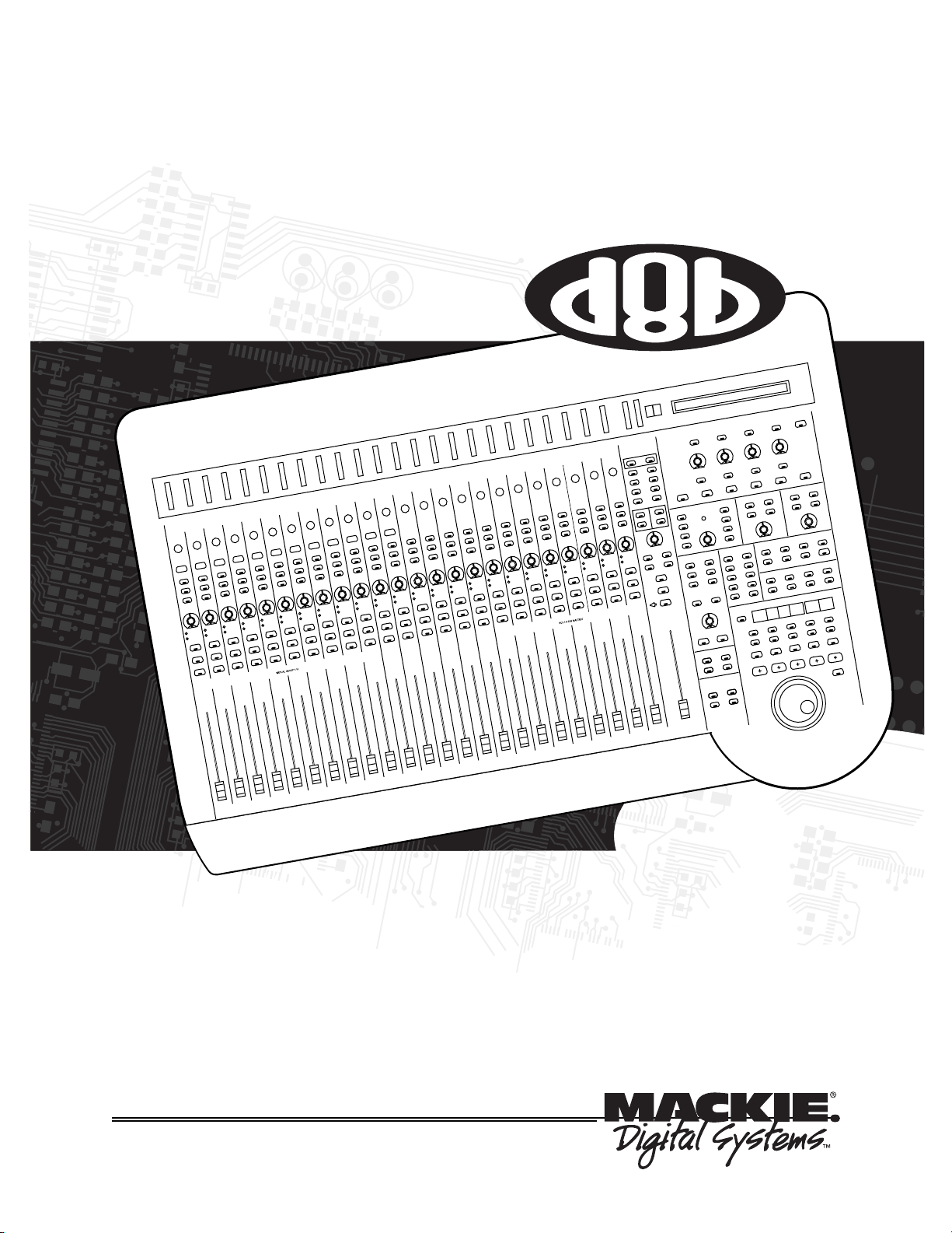
56 input, fully-automated digital mixing console.
This file contains all 110 pages of 8.5" x 11" (to make it easier to print out)
D8B
HOME
DIGITAL 8•BUS
™
SERVICE MANUAL
©1999 Mackie Designs Inc.
#820-182-00
Page 2
C AU TIO N
g
g
g
g
g
g
AVIS
RISK OF ELECTRIC SHOCK
DO NOT OPEN
RISQUE DE CHOC ELECTRIQUE
NE PAS OUVRIR
CAUTION: TO REDU CE THE RISK O F
ELECTRIC SHOCK DO NOT REMOVE
THE COVER (OR BACK)
NO US ER SERVICEAB LE PAR TS INS IDE
R EF E R S ER V IC IN G T O Q U AL IFIE D
PERSONNEL
W ARNING: TO RE DUCE THE RISK OF
FIRE OR E LEC TRIC SH OC K, DO NO T
EXPOSE THIS PROD UCT TO RAIN OR
MOISTURE
TO PREVENT ELECTRIC SHOCK, DO
NOT USE THIS POLARIZED PLUG W ITH
AN EXTENSION CORD, RECEPTACLE OR
OTHER OUTLET UNLESS THE BLADES
CAN BE FULLY INSERTED TO PREVENT
BLADE EXPOSURE.
ATTENTION: POUR EVITER LES
RISQUES DE C HOC ELECTRIQUE, NE
PAS ENLEVER LE COUVERCLE. AUCUN
ENTRETIEN DE PIECES INTERIEURES
PAR L'USAGER. CONFIER L'ENTRETIEN
A U P E R S O N N E L QU A L IF IE .
A VIS :P O U R EV IT ER L ES R IS Q UE S
D'INCENDIE OU D'ELECTROCUTION,
N'EXPOSEZ PAS CET ARTICLE A LA
PLUIE O U A L'HUM IDITE.
POUR PREVENIR LES CHOCS
ELE CTRIQ UES N E PA S UTILISER C ETTE
FICHE POLARISEE AVEC UN
PROLONG ATEUR , UN PR ISE DE
COUR ANT OU UNE AUTRE SORTIE DE
COURANT, SAUF SI LES LAMES
PEUVENT ETRE INSEREES A FOND
SANS LAISSER A UCUNE PARTIE A
DECOUVERT.
This apparatus does not exceed the Class A/Class B (whichever is applicable) lim its for radio
noise emissions from di
ital apparatus as set out in the radio interference regulations o f th e
Cana dia n De partment of Com m unica tions.
ATTENTION :Le présent appareil numérique n'ém et p as de bruits radioélectriques dépassant
las lim ites applicables aux appareils num ériques de c lass A /de class B (selon le cas) prescrites
dans le ré
le m e n t s ur le b ro u illage radioélectrique édicté par les ministere des com m unications
du Ca nada.
This equipm ent has been tested and found to com ply with the lim its for a Class A di
device, pursuant to part 15 of the FCC rules. These lim its are desi
protection a
environm ent. This equipm ent
ainst harm ful interference when the equipm ent is operated in a com mercial
enerates, uses, and can radiate radio energy a nd, if no t
ned to provide reasonable
ital
installed properly and used in acco rdance w ith the ins truction m anual, m ay ca use harm ful
int e rfe re n ce to r ad io c om m u nic a tio ns . O p e ra tio n of th is e q uip m e n t in a r es id e ntia l a r ea is lik ely
to c au s e h a rm f ul in te rf er e nc e i n w hic h c a se th e us e r w ill be r e qu ire d to co r re c t th e inte rf e re nc e
at his own expense.
The lightning flash with arrowhead symbol within an equilateral
triangle is intended to alert the user to the presence of uninsulated
"dangerous voltage" within the product's enclosure, that may be
of sufficient magnitude to constitute a risk of electric shock to persons.
Le symbole éclair avec point de flèche à l'intérieur d'un triangle
équilatéral est utilisé pour alerter l'utilisateur de la présence à
l'intérieur du coffret de "voltage dangereux" non isolé d'ampleur
suffisante pour constituer un risque d'éléctrocution.
2
The exclamation point within an equilateral triangle is intended to
alert the user of the presence of important operating and maintenance
(servicing) instructions in the literature accompanying the appliance.
Le point d'exclamation à l'intérieur d'un triangle équilatéral est
employé pour alerter les utilisateurs de la présence d'instructions
importantes pour le fonctionnement et l'entretien (service) dans le
livret d'instruction accompagnant l'appareil.
Page 3
WARNING
Service on the d8b must only be
undertaken by experienced service
technicians.
! SMD !
The d8b makes extensive use of
surface mount components.
Servicing technicians should have the
tools, experience and patience to perform
surface mount rework.
The d8b contains components that
may be damaged by elecrostatic
discharge. All standard ESD
precautions must be taken when
! ESD !
servicing.
Additional Safety Information
Mackie Designs’ Digital 8•Bus has been tested and conforms to the following standards
and directives of the European Council:
73/23/EEC Low Voltage Directive with amendments
91/263/EEC, 89/392/EEC, and 89/336/EEC
89/336/EEC EMC Directive
IEC 950(1991)/EN60950:1992 Electrical Safety Requirements
EN55103-1 and EN55103-2 Residential (E1) and Commercial (E2) Environments
Note: The following notice concerns the lithium battery located on the motherboard
inside the Remote CPU.
CAUTION: DANGER OF EXPLOSION IF BATTERY IS INCORRECTLY REPLACED. REPLACE ONLY
WITH THE SAME OR EQUIVALENT TYPE RECOMMENDED BY THE MANUFACTURER. DISPOSE OF
USED BATTERIES ACCORDING TO THE MANUFACTURER’S INSTRUCTIONS.
ATTENTION: IL Y A DANGER D’EXPLOSION S’IL Y A REMPLACEMENT INCORRECT DE LA
BATTERIE, REMPLACER UNIQUEMENT AVEC UNE BATTERIE DU MEME TYPE OU D’UN TYPE
ÉQUIVALENT RECOMMANDÉ PAR LE CONSTRUCTEUR. METTRE AU REBUT LES BATTERIES USAGÉES
CONFORMÉMENT AUX INSTRUCTIONS DU FABRICANT.
3
Page 4

CONTENTS
INTRODUCTION ......................................................................................... 5
TECHNICAL SUPPORT ................................................................................ 5
DISCLAIMER................................................................................................ 5
OVERVIEW ................................................................................................... 6
COMPUTER SYSTEM ................................................................................... 7
DSP SYSTEM ................................................................................................. 9
USER INTERFACE SYSTEM ........................................................................ 11
ANALOG SYSTEMS ................................................................................... 13
POWER....................................................................................................... 13
DSP SIGNAL FLOW, CLOCKS, MUTE ....................................................... 14
PARTS....................................................................................................... A- 1
INTEGRATED CIRCUITS AND DATA SHEETS LINKS .............................. B-1
CONNECTORS ........................................................................................ C-1
FOLD-OUT SECTIONS:
BLOCK DIAGRAMS ................................................................................. D1
EXPLODED DRAWINGS............................................................................ E1
ASSEMBLY DRAWINGS: CONSOLE ........................................................ F1
ASSEMBLY DRAWINGS: REMOTE CPU ..................................................G1
BOARD CHAPTERS (Schematics and PCB for each board)
108A Mic/line meter ........................................................... 108
109A Line/master meter .................................................... 1 09
110B Analog I/O .................................................................110
111B Power distribution ..................................................... 111
112C DCA ............................................................................ 112
113B Codec ........................................................................ 1 13
114C DSP ..............................................................................114
115E Digital I/O .................................................................. 115
119B Tape I/O ..................................................................... 119
120A Mic/control surface.................................................. 120
121A Line/control surface.................................................. 121
122A Output control surface ............................................12 2
123A Remote CPU linear power supply...........................123
124A 8-Way fader ............................................................... 124
125A 9-Way fader ............................................................... 125
136A B rain ............................................................................ 136
163C Back plane................................................................. 163
164C Clock card ................................................................. 164
201A Remote CPU power distribution.............................20 1
4
Page 5
INTRODUCTION
This manual contains service information for the d8b digital audio mixer. To service the
d8b, technicians should be familiar with op-amp based and discrete analog circuitry,
digital troubleshooting, microprocessors, digital audio, DSP, ESD, ESP, and the operation/
application of mixing consoles. Presentation of this manual does not constitute
endorsement of qualifications by Mackie Designs.
This manual is available in Adobe© Portable Document Format (PDF), as part of
Mackie Designs’ Digital Service CD-ROM (part# 820-163-00). This is available to all Service
centers authorized to repair the d8b. Also included on the CD-ROM are the schematics,
PCB layouts, parts lists, assembly drawings, some IC data sheets and the owner’s
manual.
It is essential that you become familiar with the owner’s manual as it contains all of
the operational details, hookup diagrams, specifications and just about everything
d8bwegian. It will be a great help for you to verify customers complaints, and to check
for correct operation.
This service manual does not include an in-depth circuit analysis, rather it provides an
overall guide to details not immediately obvious from the schematics alone. It is
intended to help you troubleshoot down to board level and identify and swap out any
bad circuit boards. Component level troubleshooting down to resistor or IC level, may
be undertaken if time permits, or if there appears to be something obvious.
SERVICE TECHNICAL ASSISTANCE
Mackie Designs, Service Technical Assistance, is available 8AM - 5PM PST, Monday through
Friday for Authorized Mackie Service Centers, at 1-800-258-6883. Feel free to call with any
questions and speak with a carefully-calibrated technician. If one is not available, leave
a detailed message and a qualified Mackoid will return your call asap.
DISCLAIMER
The information contained in this manual is proprietary to Mackie Designs, Inc. The entire
manual is protected under copyright and may not be reproduced by any means without
express written permission from Mackie Designs Inc.
GETTING STARTED
Upon receiving a d8b for repair, your first impression may be to run screaming into the
night. After reading this overview, checking the schematics, pcb layouts, assembly
drawings, parts lists, having a good look at the owner’s manual and inspecting the unit,
you will probably realize that your first impression was correct.
Think of the remote CPU as a standard PC with extra power supplies for the console.
Standard PC troubleshooting techniques and commercially available diagnostic DOS
software can be applied to repair the remote CPU.
In its simplest form, the mixer and the remote CPU are two boxes full of circuit boards,
all joined together with lots of connectors and ribbon cables. A preliminary inspection
will often reveal a simple problem, such as a bad connection somewhere, a loose cable,
a bad switch or control, or the CPU’s CMOS settings may need to be reset.
Our technical support team are available to discuss any d8b problems and offer
solutions. If you ever suspect that a customer’s complaint is related to the version of
Mackie software they are using, you should consult with your customer and Mackie
Designs before downloading the latest software from our website: www.mackie.com
5
Page 6
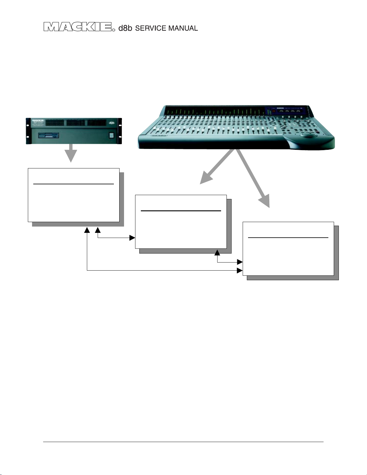
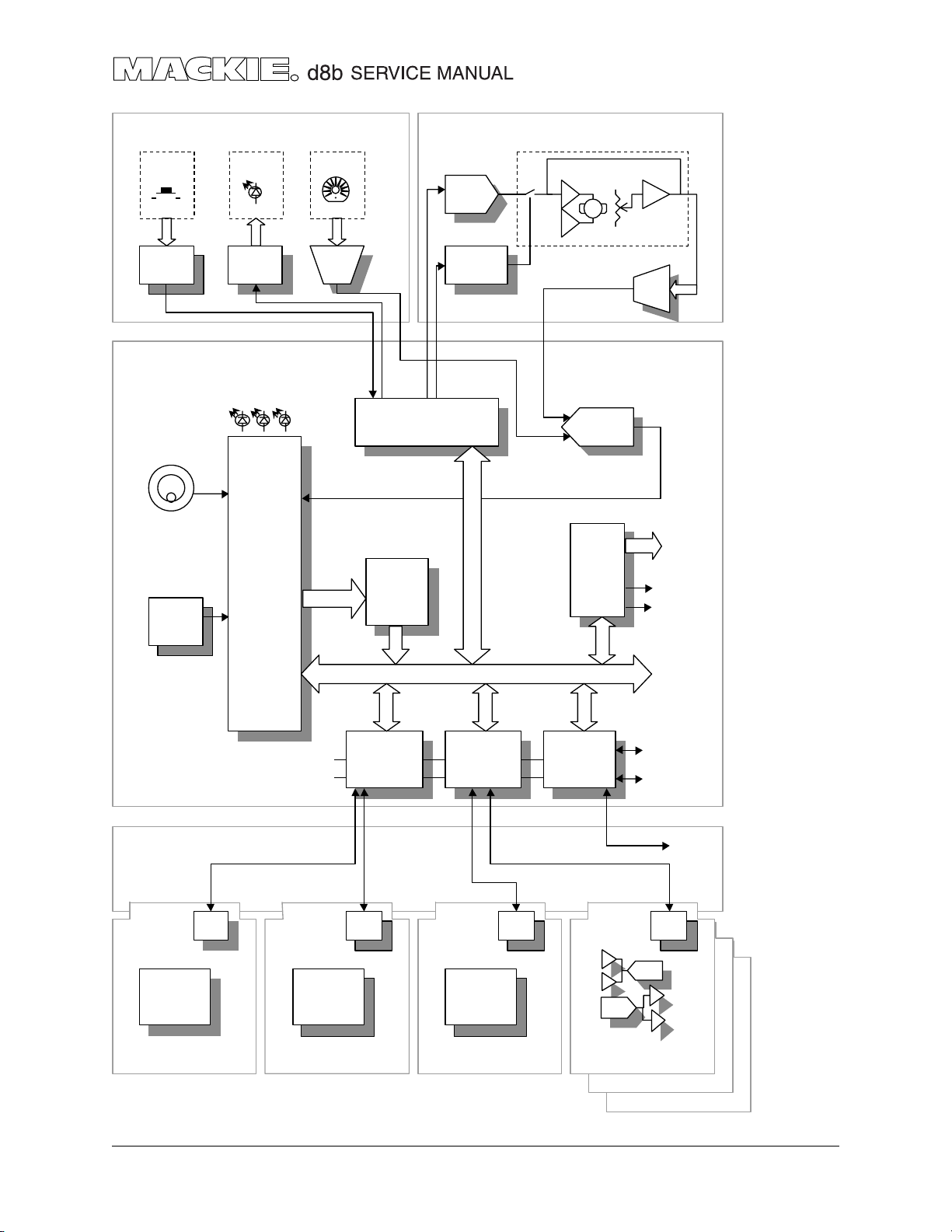
OVERVIEW
The ‘Digital’ functions of the d8b can be broken down into 3 main systems; Computer,
DSP, and User Interface. The computer is a Pentium system which is contained in the
Remote CPU with the Power Supply . It communicates via standard com ports (RS-232)
to the DSP and UI systems in the console.
Remote CPU
Pentium PC
HDD, Floppy, Video
DSP
A/D – D/A converters,
24 on board DSP chips,
FX cards, I/O Cards
meters
U
ser Interface
(control surface)
Switches, V-pots, LEDs,
Flying Faders, Displays
The computer runs Mackie’s real time operating system and handles functions normally
associated with a PC such as keyboard, mouse, disk drives, video, etc. The DSP system
controls all Digital Signal Processing functions in the console. The User Interface system
reads and updates the control surface.
Commands from the UI are looped through the computer. For example, if the Mute
button on channel 1 is pressed, the UI system detects it and communicates the event to
the computer. The computer then tells the DSP system to mute CH-1, and tells the UI
system to light CH-1’s mute LED. Note that the LED is not lit by the UI system directly.
Commands can also be issued by clicking on the monitor screen (GUI). Note: the DSP
communicates the meter information directly to the UI, not looped through the
computer.
6
Page 7

COMPUTER SYSTEM
HARDWARE
The computer system within the Remote CPU chassis consists of the following hardware;
• Computer motherboard
• Computer microprocessor
• RAM
• HDD, FDD
• Ethernet® Card
• SVGA Video Card
• MIDI Card, SMPTE
These are all standard PC compatible parts. However, because the drivers are written
into the Mackie OS, other similar devices may not be compatible. Also, it should be
noted that ‘upgrading’ the processor, RAM, or HDD is of little value as the Mackie OS will
not take advantage of it.
EXTRA CIRCUITRY
Circuit boards inside the Remote CPU, which are not normally found inside a standard
PC are: extra power supplies, AC line and fusing circuits, chicken soup machine etc.
• Mackie board 201 is the remote CPU’s power distribution
• Mackie board 123 is a Linear power supply for the consoles analog functions
• An OEM 5V supply for the consoles digital functions
SOFTWARE
The d8b’s computer runs Mackie’s real time operating system.
THERE IS NO MS-DOS OR WINDOWS IN THE SYSTEM!
You will not find COMMAND.COM, CONFIG.SYS, or AUTOEXEC.BAT anywhere on the hard
drive. After the BIOS starts, the system boots directly into the Mackie Operating System.
CMOS setup can be accessed as in a regular PC.
The Mackie OS also contains the operating software for the DSP and UI systems. Most
future upgrades can be done without swapping EPROMS.
Please talk to our technical support team to discuss the d8b problems you are
experiencing. There is a good chance that a customer’s complaint may be cured by
upgrading to the latest sotware version. You will first need the customer’s permission
before downloading any upgrades from our website (www.mackie.com).
TROUBLESHOOTING THE COMPUTER
A common error message you might see is “System Error 43 - Host did not boot.”
The possible reason for this may be:
• The computer did not get through BIOS correctly.
• A static charge may have reset your BIOS CMOS settings.
• The data cable between the computer and the console is not connected, or is
not a straight through 25 pin din connecter.
Possible Solution:
• Connect a keyboard and monitor and press F1 to enter the computer’s BIOS
during a boot.
• Once inside the BIOS, use the AUTODETECT hard drive menu and this will likely fix
the errors you are having, once the detected drive information is saved.
(See also the notes on the following page).
7
Page 8

CMOS SETUP
If you encounter “System Error 43,” Check the following CMOS setup which you can reach
during bootup by pressing Del (or F1 depending on the age of the console).
• Enter the standard CMOS setup screen, change the Primary Master to AUTO
• Next go to the Advanced CMOS setup and check the following:
(highlight and use PgUp/PgDn to modify).
Ist Boot Device ..................... Floppy
2nd Boot Device .................. IDE-0
3rd Boot Device ................... Disabled (CD-ROM)
4th Boot Device ................... Disabled
Try other Boot Devices......... Yes
S.M.A.R.T for Hard Disks........ Disabled
Quick Boot ............................ Enabled
When you have finished checking and/or making any corrections, press F10 to save the
settings and exit. Then Reboot and see if this has done the trick, and the “System Error 43”
has gone away.
NOTE: from November 1999 (serial numbers with prefix “BS11954” or higher), the
motherboard changed to 480-039-00, and there are different CMOS settings:
Press and Hold <Delete> key to go to BIOS Setup program
Using the arrow keys, select STANDARD CMOS SETUP, Press <Enter> (“Page Up” and
“Page Down” keys, and number pad can be used to change BIOS values).
Change the Date to current day, month, year. Press <Enter>
Change Time to current time (24-hour clock), Press <Enter>
Make sure all HARD DRIVES on table are set to “AUTO” MODE
Change “Halt On:” to “All, But Keyboard”, Press <Enter>
Back out to root menu by pressing <Esc>
Select “BIOS FEATURE SETUP” and make sure “Boot Sequence” is “A,C,SCSI”. <ESC>
Select CHIPSET FEATURES SETUP, Press <Enter>
Change “PCI 2.1 Compliance” to “Enabled”.
Change “Spread Spectrum” to “Enabled” and then <ESC> to main BIOS menu.
Select INTEGRATED PERIPHERALS, <Enter>
Change “Init Display First” to “PCI Slot”, <Enter>
Make sure “Onboard Serial Port 1” is set to “3F8/IRQ4” and “Onboard Serial Port 2”
is set to “2F8/IRQ3”, then press <ESC> to return to the main BIOS menu.
Select SAVE & EXIT SETUP. Type “Y” for yes, <Enter>
Bootup Num Lock................ On
Floppy Drive Swap............... Disabled
Floppy Drive Seek................. Enabled
PS/2 Mouse support ............. Auto
System Keyboard.................. Absent
Primary Display ..................... VG A/ EG A
Password Check .................. Setup
FURTHER TROUBLESHOOTING
If the CMOS setup is correct and a problem still remains, you will have to delve into the
Remote CPU and troubleshoot the computer system.
The computer can be booted with a DOS system floppy for running all of your favorite
DOS diagnostic programs. To do this:
• Find or make a bootable floppy, i.e. one which has the DOS system installed.
• Place the disc in the drive before turning on the Remote CPU.
• The computer should start up into DOS from this disc, rather than from the Mackie
OS.
• Insert any standard DOS diagnostic software and run tests, for example on the
hard drive, video card, mother board etc.
Check the extra Mackie power supply voltages are correct, as shown on the
schematic chapters 201 (power distribution) and 123 (Linear power supply). Also check
the voltages on the console end: see the console power distribution board chapter 111.
8
Page 9
DSP SYSTEM
A simplified block diagram of the DSP system is shown on the next page. At the heart of
the system is an Analog Devices ADSP-2181. It acts as the console CPU, and controls all
functions and communications within the DSP system. There are 24 proprietary DSP chips
to handle the actual audio processing. Parallel processing with the 24 DSPs allows the
d8b to complete all processing within one sample.
Operating instructions are loaded from the Remote CPU as the system boots. The
EPROM does not contain operating firmware. Think of the EPROM as BIOS, it provides the
system with basic instructions to make sure it powers up correctly and sets up to receive
the operating software from the Remote CPU.
CLOCKS
All audio clocks for the DSP system originate at the clock (sync) card. The master clock is
512 x sample rate. See page 24 for some more details.
CODEC BOARD
The CODEC board contains 24 channels of A/D and D/A. Each ADC converts two
analog audio signals into a two channel serial format which is sent to the DSP chips. All
digital audio signals within the d8b are in this two channel format. The DACs convert this
stream back to 2 channels of lovely analog audio.
DSP BOARD
Each of the 24 DSP chips has two serial inputs, DR_0 and DR_1, and two serial outputs,
DT_0 and DT_1, a total of 48 inputs and 48 outputs (remember that each serial input is 2
channels of audio, so that’s 96 channels!, but they’re not all used). Digital audio data
comes from and is sent to the CODEC board, I/O cards, and FX cards.
Y2 is the processor clock from which is derived CLK_1, CLK_2, CLK_3, CLK_4 and CLKIN.
Y1 is a UART clock.
The processing algorithm works in such a way that each serial output consists of one
mix and one direct output. In order to route mixes to the same DACs the serial data is
juxtaposed in sync with the L/R clock.
There are three status indicators on the board: D2 (green),D3 (yellow), D1 (red).
DSP INPUTS DSP OUTPUTS
12 Mic/Line Inputs 8 Subgroups
12 Line Inputs 2 L/R Mix
24 Tape Input Cards 24 Tape Returns Cards
16 FX Card Returns 16 FX Card Sends
2 Meter (monitor) 12 Aux sends
8 Alt Input Card 8 Alt Output Card
2 Solo
•If all three are on, a fault has been detected.
•If the red LED is on solidly, then this is operating OK.
9
Page 10
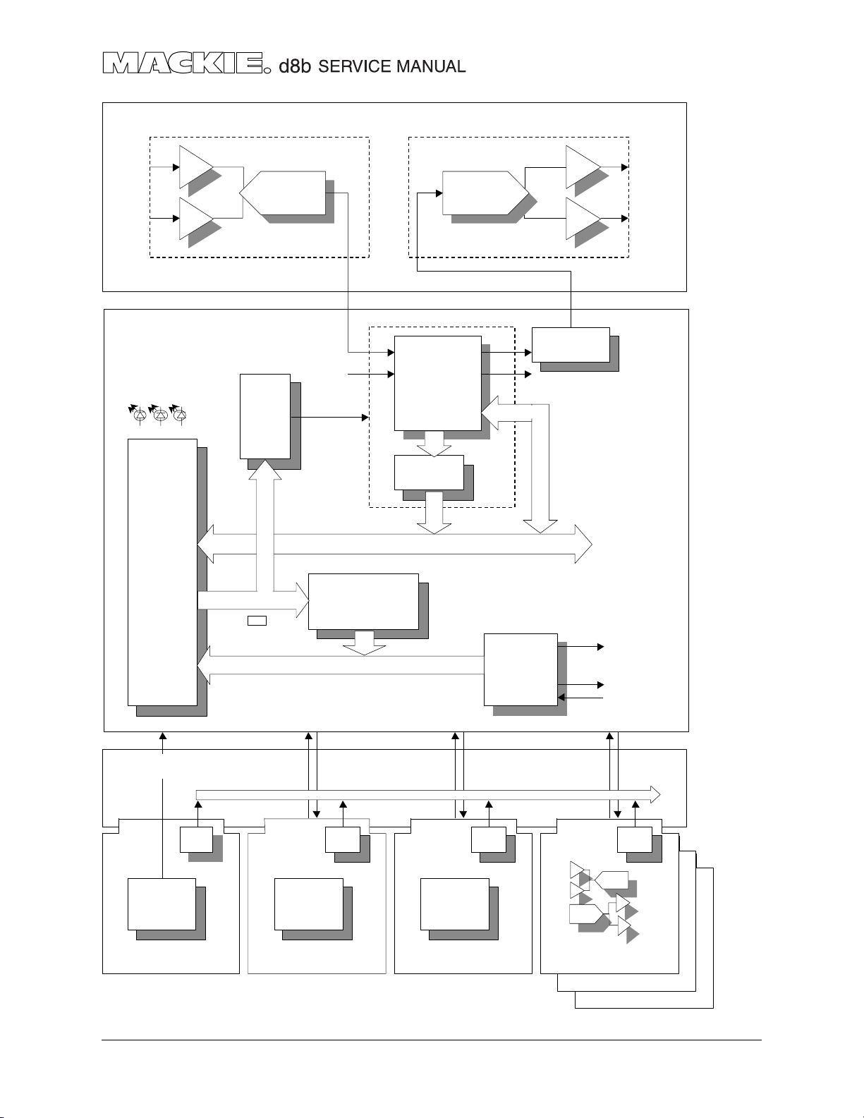
CODEC BOARD -113
ANALOG
AUDIO
INPUTS
DSP BOARD -114
STATUS LEDS
ADSP-2181
CPU-DSP
ADC
x13 x12
DSP
CHIP
SELECT
IAD0-IAD15
A0-A13
EPROM
DAC
DR0 DT0
DR1
LATCH
DSP
DT1
x24
WOOP-DEE
ANALOG
AUDIO
OUTPUTS
x6
BACKPLANE BOARD -163
PIC PICPICPIC
DSP
CLOCK
D8-D23
FX
DSP
EFFECTS CARD
AES/EBU
AES/EBU CARD -115 TAPE I/O CARD -119CLOCK CARD -164
UART
TO PC COM-2
DSP_TX
DSP_RX
TO BRAIN
ADC
DAC
APOGEE I/O CARD
AES/EBU 8-CH I/O CARD
BOARD
x4
10
Page 11
UI SYSTEM
A simplified block diagram of the User Interface system is shown on the next page. Like
the DSP system, an Analog Devices ADSP-2181, is used as the CPU. It controls all functions
and communications within the UI system. Also, like the DSP system, operating
instructions are loaded from the Remote CPU as the system boots. If the UI system does
not ‘find’ the Remote CPU, it will display ‘ERROR 43 HOST COMPUTER NOT FOUND’ in the
VFD.
CLOCKS
Unlike the DSP system, the UI system runs on its own clock. The Clock (Sync) card is for the
DSP system only. Keep the clock’s main spring wound up.
BRAIN BOARD
The Brain Board reads in two types of information from the control surface. Switches are
scanned in through PISO shift registers and transferred to the Brain as serial data. Analog
voltages from faders and V-pots are multiplexed, then sent to an ADC on the Brain
board.
The Brain Board also communicates via UART to all expansion cards. Every card used
in the d8b has a PIC chip. The PIC chip outputs a copyrighted text string so that the d8b
can verify the card is original and Mackie-authorized. Cards in which operating
parameters can be varied are controlled via the Brain (UI System). The Brain Board also
controls all functions on the DCA board.
X1 is the brain processor clock, X2 and X3 are UART clocks.
The Brain board has three status indicators: D3 (green),D2 (yellow), D1 (red).
CONTROL SURFACE
Control surface LEDs, including V-pot indicators, are updated via SIPO shift registers. To
control the fader motors, serial data is sent from the Brain board to a DAC on the fader
board.
VU METERS
The VU meter LEDs are updated via shift registers but function differently than the control
surface. Remember that the control surface commands are looped through the
Remote CPU; VU meter information is not. The information for the VU meters comes
directly from the DSP Board, and is communicated to the Brain Board via UART.
• If they are all on, it did not read the
EPROM.
• If only the green is on, then it read
the EPROM but did not download
the software.
• When it is running correctly, only the
red LED should be on (and blinking).
11
Page 12
CONTROL SURFACE -120 -121 -122
SWITCHES LEDS V-POTS
SHIFT
REGISTERS
SHIFT
REGISTERS
MUX
BRAIN BOARD -136
FADER BOARDS -125 -125
DAC
SHIFT
REGISTERS
FLYING
FADERS
x 25
MUX
STATUS LEDS
JOG
WHEEL
ADSP-2181
CPU-DSP
SYSTEM
CLOCK
BACKPLANE BOARD -163
A0-A13
CLK1
CLK2
LATCHS
I/O BUFFERS
EPROM
D8-D23
UARTUART
ADC
LATCHES
I/O BUFFERS
UART
TO VFD
DRIVER
VU METERS
DCA BOARD
PC COM-1
RS232
DSP
12
PIC PICPICPIC
DSP
CLOCK
FX
DSP
EFFECTS CARD
AES/EBU
AES/EBU CARD -115 TAPE I/O CARD -119CLOCK CARD -164
ADC
DAC
APOGEE I/O CARD
AES/EBU 8-CH I/O CARD
x4
Page 13

ANALOG SYSTEMS
NOTE: The Bus numbers as written on the schematics for the CODEC and DCA
board are reverse numbered by the software. So Bus 1 on the schematic is
really Bus 8, Bus 2 is really Bus 7, Bus 3 = 6, Bus 4 = 5, Bus 5 = 4, Bus 6 = 3,
Bus 7 = 2 and Bus 8 = 1.
The analog circuits used in the d8b should be familiar to anyone with experience
servicing Mackie products. The 12 Mic Pre’s are the same circuit which is used in the
SR40•8. The line amps use Mackie’s ‘unity plus’ architecture.
DCA BOARD
As the name suggests, the DCA board contains Digital Controlled Amplifiers to control
the level of analog signals in the console’s monitor section. The DCA board also
contains an analog switching matrix to select and route monitor signals. The Brain Board
controls switching and level functions on the DCA Board. DCAs are controlled by a serial
data line. Analog switches are controlled by SIPO shift registers, except for TALK and
PUNCH which are controlled directly by the Brain board’s CPU.
POWER
POWER SUPPLIES
There are three power supplies within the Remote CPU chassis. A standard PC power
supply for the Pentium Motherboard, a +5V, 100W OEM switching supply for the console’s
digital functions, and an analog supply for the console’s analog functions.
The PC supply and the OEM supply should be treated as ‘black boxes’ and swapped
if bad. The analog supply is nearly identical to the design used in the SR24•4,
troubleshooting should be fairly straightforward.
POWER DISTRIBUTION
In the console, power is sent from the Power Distribution Board (111) to the Brain, DSP,
Backplane, and Analog I/O boards. These boards then distribute power to the remaining
boards.
Note: there are many bypass capacitors used throughout the console. If one of the
power supply rails is low or intermittent, one of these may have shorted, but it not an
easy thing to find which one. It will be a great help if you have a low impedance ohm
meter. You should then be able to narrow in on the offending cap or ferrite.
NOTE:
The d8b keeps the same jumper designations for all PCBs, Hurrah! So J35 on the output
board is also J35 on the Brain board. See the connectors chapter for complete details of
every connector and pinout used in the console.
If the d8b has optional I/O cards installed, use a slotted screwdriver to make sure the
installation screws are tightly secured, and not just finger-tight.
13
Page 14
DSP SIGNAL FLOW
The DSP board is the central hub of the signal flow system, the digital signals must find their way to the
DSP board, get DSP’d and make their way out again to the big audio ocean.
Please take a look at the Block diagrams chapter, especially the diagram on page D3, and the DSP
map on the next page. Also see the connectors chapter for details of every connector and pinout.
Signal names (golden rule)
Throughout the console, you will see digital signal names beginning with DR and DT. Anything which
starts with DR is a digital signal on its way to the DSP board, any signal which starts with DT has come from
the DSP board. Do not be surprised to see a few of the signals change name or number as they go from
one board to the next, (but the DT or DR start part will not change).
Analog input signals
Analog audio signals coming from the Line inputs or Mic inputs are converted to digital by the CODEC
board. Each pair of analog signals is combined to form one digital serial stream (DR) sent to the DSP. There
are a total of 12 digital signals (from 12 analog pairs)
Analog audio signals from the Tape cards are converted to digital by the Tape card’s own D/A
converters, and also paired to form digital data (DR) sent to the DSP board. Each Tape card has 8 audio
inputs and this yeilds 4 digital signals per card, or a total of 12 digital signals from the three tape cards.
Digital input signals
Digital input signals coming in from the standard Digital I/O card and the PDI•8 digital I/O card are
passed to the DSP board (DR). The incoming signals are already in the 2 channel digital serial form. The
standard Digital I/O card has 1 digital input, the PDI•8 card has 4.
Digital input and output signals from the effects cards
There are slots for up to four effects cards. Each card can send and receive two digital signals to and
from the DSP board.
DR (data received by DSP)
Digital data received by the DSP board for processing is labelled starting with DR. Each of the 24 DSP
ICs can receive two digital data streams, so you will see DR0_ and DR1_, followed by which DSP IC is used,
such as U1 , U3 or U24.
DT (data transmitted by DSP)
Digital data which is transmitted by the DSP board is labeled starting with DT. Each of the 24 DSP ICs
can transmit two outputs DT0_ and DT1_.
12 digital signals go to the CODEC board to become these analog signals: 8 Buses, Mix L, Mix R, Solo L,
Solo R and 12 Auxes.
12 digital signals go to the 3 Tape Cards (which have their own A/D convertors) to become 24 analog
tape outputs.
8 digital signals go to the 4 Effects cards, 1 goes to the Digital I/O and 4 to the PDI•8 I/O card. The
signals to the I/O cards are not converted to analog, but pass out of the digital output connectors on the
rear panel of each card for digital recording. Note that each signal is still really a pair such as L/R.
14
DSP SIGNAL FLOW
Page 15
DSP map
This table shows the data received (DR) and data transmitted (DT) by the DSP board. On a scale of 1
to 10, you will find this table fairly useful.
INPUT ADC SIG CABLE DSP JUXT SIG NAME(DSP) CABLE SIG NAME DAC OUTPUT
LINE 13+14 CODEC U3 DR1 J13-3 DR0_U1 DT0_U1 U46 (DT0_U2) DT_1 J13-1 DT1 CODEC U52 BUS 1+2
FX-1 J24-23 DR1_U1 DT1_U1 J24-1 DT1_U1 FX-1
LINE 15+16 CODEC U103 DR2 J13-7 DR0_U2 DT0_U2 U46 (DT0_U1) DT_2 J47-2 DT_2 TAPE I/O TAPE 17+18
FX-1 J24-25 DR1_U2 DT1_U2 J21-13 DT1_U2 FX-1
LINE 17+18 CODEC U203 DR3 J13-11 DR0_U3 DT0_U3 U46 (DT0_U4) DT_3 J13-5 D T2 CODEC U152 BUS 3+4
FX-2 J24-7 DR1_U3 DT1_U3 J24-5 DT_3 FX-2
LINE 19+20 CODEC U303 DR4 J13-15 DR0_U4 DT0_U4 U46 (DT0_U3) DT_4 J47-6 DT_4 TAPE I/O TAPE 19+20
FX-2 J24-9 DR1_U4 DT1_U4 J21-15 DT1_U4 FX-2
LINE 21+22 CODEC U403 DR5 J13-19 DR0_U5 DT0_U5 U86 (DT0_U6) DT_5 J13-9 D T3 CODEC U252 BUS 5+6
FX-3 J24-13 DR1_U5 DT1_U5 J24-11 DT_5 FX-3
LINE 23+24 CODEC U503 DR6 J13-23 DR0_U6 DT0_U6 U86 (DT0_U5) DT_6 J47-10 DT_6 TAPE I/O TAPE 21+22
FX-3 J24-15 DR1_U6 DT1_U6 J21-17 DT1_U6 FX-3
RET 1+2 CODEC U603 DR7 J13-27 DR0_U7 DT0_U7 U86 (DT0_U8) DT_7 J13-13 DT4 CODEC U352 BUS 7+8
FX-4 J24-19 DR1_U7 DT1_U7 J24-17 DT_7 FX-4
RET 3+4 CODEC U703 DR8 J13-31 DR0_U8 DT0_U8 U86 (DT0_U7) DT_8 J47-14 DT_8 TAPE I/O TAPE 23+24
FX-4 J24-21 DR1_U8 DT1_U8 J21-19 DT1_U8 FX-4
RET 5+6 CODEC U803 DR9 J12-3 DR0_U9 DT0_U9 U89 (DT0_U10) DT_9 J13-17 DT5 CODEC U452 L/R MIX
ALT I/O J48-21 DR1_U9 DT1_U9 J48-19 DT1_U9 ALT I/O
RET 7+8 CODEC U903 DR10 J12-7 DR0_U10 DT0_U10 U89 (DT0_U9) DT_10 J47-19 DT_10 TAPE I/O TAPE 9+10
ALT I/O J48-25 DR1_U10 DT1_U10 J48-23 DT1_U10 ALT I/O
RET 9+10 CODEC U1003 DR11 J12-11 DR0_U11 DT0_U11 U89 (DT0_U12) DT_11 J13-21 DT6 CODEC U552 L/R SOLO
ALT I/O J48-29 DR1_U11 DT1_U11 J48-27 DT1_U11 ALT I/O
RET 11+12 CODEC U1103 DR12 J12-15 DR0_U12 DT0_U12 U89 (DT0_U11) DT_12 J47-23 DT_12 TAPE I/O TAPE 11+12
ALT I/O J48-33 DR1_U12 DT1_U12 J48-31 DT1_U12 ALT I/O
TAPE IN 17+18 I/O CARD J47-4 DR0_U13 DT0_U13 U92 (DT0_U14) DT_13 J13-25 DT7 CODEC U652 AUX 1+2
DR1_U13 DT1_U13
TAPE IN 19+20 I/O CARD J47-8 DR0_U14 DT0_U14 U92 (DT0_U13) DT_14 J47-27 DT_14 TAPE I/O TAPE 13+14
DR1_U14 DT1_U14
TAPE IN 21+22 I/O CARD J47-12 DR0_U15 DT0_U15 U92 (DT0_U16) DT_15 J13-29 DT8 CODEC U752 AUX 3+4
DR1_U15 DT1_U15
TAPE IN 23+24 I/O CARD J47-16 DR0_U16 DT0_U16 U92 (DT0_U15) DT_16 J47-31 DT_16 TAPE I/O TAPE 15+16
DR1_U16 DT1_U16
TAPE IN 9+10 I/O CARD J47-21 DR0_U17 DT0_U17 U95 (DT0_U18) DT_17 J12-1 DT9 CODEC U852 AUX 5+6
DR1_U17 DT1_U17
TAPE IN 11+12 I/O CARD J47-25 DR0_U18 DT0_U18 U95 (DT0_U17) DT_18 J48-2 DT_18 TAPE I/O TAPE 1+2
DR1_U18 DT1_U18
TAPE IN 13+14 I/O CARD J47-29 DR0_U19 DT0_U19 U95 (DT0_U20) DT_19 J12-5 DT10 CODEC U952 AUX 7+8
DR1_U19 DT1_U19
TAPE IN 15+16 I/O CARD J47-33 DR0_U20 DT0_U20 U95 (DT0_U19) DT_20 J48-6 DT_20 TAPE I/O TAPE 3+4
DR1_U20 DT1_U20
TAPE IN 1+2 I/O CARD J48-4 DR0_U21 DT0_U21 U98 (DT0_U22) DT_21 J12-9 DT11 CODEC U1052 AUX 9+10
DR1_U21 DT1_U21
TAPE IN 3+4 I/O CARD J48-8 DR0_U22 DT0_U22 U98 (DT0_U21) DT_22 J48-10 DT_22 TAPE I/O TAPE 5+6
DR1_U22 DT1_U22
TAPE IN 5+6 I/O CARD J48-12 DR0_U23 DT0_U23 U98 (DT0_U24) DT_23 J12-13 DT12 CODEC U1152 AUX 11+12
DR1_U23 DT1_U23
TAPE IN 7+8 I/O CARD J48-16 DR0_U24 DT0_U24 U98 (DT0_U23) DT_24 J48-14 DT_24 TAPE I/O TAPE 7+8
DR1_U24 DT1_U24
This is data going into the
DSP board.
This is Data on the DSP board,
showing which DSP does what.
This is Data transmitted by the DSP
NOTE: some of the signal names
completely change name at the
connectors, especially J12 and J13.
See the CODEC map
15
DSP SIGNAL FLOW
Page 16
J12
Digital data to
and from CODEC
Digital data to
and from CODEC
To and from
BACKPLANE
(Clock, Effects
and Digital I/O data)
To and from
BACKPLANE
(Effects data)
NOTE: UNMUTE is
a very important
line
To and from
BACKPLANE
(Tape I/O data)
To and from
BACKPLANE
(Tape I/O and
Alt I/O Data)
REMOTE CPU
(serial port)
J21
J48
J25
J47
J13
J24
J47
J48
J21
J24
J42
J25
J13
J12
J1
DSP 114
DSP CONNECTORS
This is a compilation of all the DSP board’s
connectors, mainly showing the data received and
transmitted, and clocks. The power and ground pins
are not shown here, to make things a little clearer.
These can be found in the connectors chapter, or on
the schematics.
16
DSP SIGNAL FLOW
Page 17
CODEC BOARD
IC Connector/pin
Analog
OUT
U52
U152
U252
U352
U452
U552
U652
U752
U852
U952
U1052
U1152
MIX-L MIX-R DT5
SOLO-L SOLO-R DT6
AUX-1 AUX-2 DT7
AUX-3 AUX-4 DT8
AUX-5 AUX-6 DT9
AUX-7 AUX-8 DT10
AUX-9 AUX-10 DT11
AUX-11 AUX-12 DT12
Analog
OUT
BUS-2 DT1BUS-1
BUS-4 DT2BUS-3
BUS-6 DT3BUS-5
BUS-8 DT4BUS-7
DT
from DSP
How it is labeled
out of DSP board
DT_1
DT_3
DT_5
DT_7
DT_9
DT_11
DT_13
DT_15
DT_17
DT_19
DT_21
DT_23
J13-1
J13-5
J13-9
J13-13
J13-17
J13-21
J13-25
J13-29
J12-1
J12-5
J12-9
J12-13
The Data transmitted
(DT) from the DSP board
is converted to Analog
and split out into its two
component signals. For
example, DT_1 comes
off the DSP board to the
CODEC (using J13 pin 1),
where it is renamed DT1.
U52 converts DT1 into
analog signals BUS-1
and BUS-2.
The analog signals, such
as Bus, Aux, Mix and Solo
then go off to the DCA
board via J11
IC DR to DSP
Analog
IN
U3
U103
U203
U303
U403
U503
U603
U703
U803
U903
U1003
U1103
U4
METER-L METER-R METER_DR
Analog
IN
LINE-14 DR1LINE-13
LINE-16LINE-15
LINE-18LINE-17
LINE-20LINE-19
LINE-22 DR5LINE-21
LINE-24LINE-23
RET-2RET-1
RET-4RET-3
RET-6 DR9RET-5
RET-8RET-7
RET-10RET-9
RET-12RET-11
DR2
DR3
DR4
DR6
DR7
DR8
DR10
DR11
DR12
How it is labeled
into DSP board
DRO_U1
DRO_U2
DRO_U3
DRO_U4
DRO_U5
DRO_U6
DRO_U7
DRO_U8
DRO_U9
DRO_U10
DRO_U11
DRO_U12
METER_DR
Connector
/pin
J13-3
J13-7
J13-11
J13-15
J13-19
J13-23
J13-27
J13-31
J12-3
J12-7
J12-11
J12-15
J13-33
Analog signals are
converted to digital
and combined in pairs.
This gives the Data
Received (DR) which
goes off to the DSP
board.
For example, analog
signals Line 13 and Line
14 are converted by U3
on the CODEC board to
become digital signal
DR1. This passes to the
DSP board via J13 pin 3,
where it is renamed
DRO_U1.
17
DSP SIGNAL FLOW
Page 18
CODEC connectors
This is a compilation of all the CODEC
board’s connectors, mainly showing
the analog inputs, data received and
transmitted. The power,ground and
clocks are not shown, but they can be
found in the connectors chapter, or on
the schematics.
J1
Analog signals
coming in from
Analog I/O
J3
Analog signals
coming in from
control surface
J11 J3
J15
J2
Analog signals
going out
to Analog I/O
CODEC 113
J13
J12
J2 J1
J13
Digital signals
DT=from DSP
DR=to DSP
J12
18
DSP SIGNAL FLOW
J11
Analog signals
going out
to DCA
Page 19
DCA connectors
J11
Analog signals
coming in from
CODEC board
J10
Analog signals
going out to
Analog I/O
This is a compilation of all the DCA
board’s connectors, mainly showing
the analog inputs, data received and
transmitted.
The DCA board receives the analog
Buses, Auxes, Mixes and Solos from the
DSP board, then outputs (under
control by the Brain board) to the
Analog I/O board and Bus out.
J8
Analog signals,
going to rear panel
8 BUS OUT
J9
Analog signals
going out to
Analog I/O
J8
J10J11 J9
J60
DCA 112
J31
J31
To Brain
19
DSP SIGNAL FLOW
Page 20
TAPE CARDS
This shows the analog inputs and outputs on the Tape cards. The analog signals go in and out of the
rear panel DB25 connectors J101 and J102 respectively.
The Tape cards have their own D/A and A/D converters, therefore, only digital signals are passed to
and from the DSP board.
Pairs of analog inputs are converted to digital form, for example, input 8 and 7 are combined to form
digital signal DR4 which goes off to the DSP board. DT4 comes back from the DSP board, and is converted
to analog outputs 7 and 8.
NOTE: the digital signals shown below are named as they appear on the Tape card only. The names
are changed at the backplane board before going to the DSP baord. See the next page for details.
This shows the
digital signals
from the DSP
board, and the
analog output
signals they
become after
D/A conversion.
For example,
digital signal DT4
on the Tape card
comes from the
DSP board. This is
converted, and
becomes analog
signal 8 and
analog signal 7.
These appear on
the DB25 output
connector J102
for recording.
ANALOG
OUTPUT
8 GND
6 GND
5_OUT_COLD DT3
4_OUT_COLD DT2
4 GND
3_OUT_COLD DT2
2_OUT_HOT DT1
2 GND
1_OUT_COLD DT1
7 GND
6_OUT_COLD DT3
5_OUT_HOT DT3
DIGITAL
NAME
DB25
Connector/pin
DT48_OUT_HOT
DT47_OUT_COLD
DT36_OUT_HOT
J102-1
J102-2
J102-3
J102-4
J102-5
J102-6
J102-7
J102-8
J102-9
ANALOG
INPUT
8 GND
6 GND
5_IN_COLD DR3
4_IN_COLD DR2
4 GND
3_IN_COLD DR2
DIGIT AL
NAME
DR48_IN_HOT
DR47_IN_COLD
DR36_IN_HOT
DB25
Connector/pin
J101-1
J101-2
J101-3
J101-4
J101-5
J101-6
J101-7
J101-8
J101-9
This shows the
analog signals
coming in from a
tape deck, and
the digital signals
they become
after A/D
conversion.
For example,
analog signals 8
and 7 come in on
the tape card’s
DB25 input
connector J101
J102-10
J102-11
2_IN_HOT DR1
2 GND
J101-10
J101-11
and are
converted to
become digital
J102-12
J102-13
DT48_OUT_COLD
DT47_OUT_HOT
J102-14
J102-15
J102-16
J102-17
J102-18
1_IN_COLD DR1
DR48_IN_COLD
DR47_IN_HOT
7 GND
6_IN_COLD DR3
5_IN_HOT DR3
J101-12
J101-13
J101-14
J101-15
J101-16
J101-17
J101-18
signal DR4. This
then goes to the
DSP board for
processing.
5 GND
4_OUT_COLD DT2
3_OUT_HOT DT2
3 GND
2_OUT_COLD DT1
1_OUT_HOT DT1
1 GND J102-25
20
DSP SIGNAL FLOW
J102-19
J102-20
J102-21
J102-22
J102-23
J102-24
5 GND
4_IN_COLD DR2
3_IN_HOT DR2
3 GND
2_IN_COLD DR1
1_IN_HOT DR1
1 GND J101-25
J101-19
J101-20
J101-21
J101-22
J101-23
J101-24
Page 21
TAPE CARDS continued
ANALOG
TAPE OUTPUT
PAIRS
23 AND 24
21 AND 22
19 AND 20
17 AND 18
15 AND 16
13 AND 14
11 AND 12
9 AND 10
7 AND 8
5 AND 6
3 AND 4
1 AND 2
DIGITAL SIG
NAME ON
TAPE BOARD
DT4
DT3
DT2
DT1
DT4
DT3
DT2
DT1
DT4
DT3
DT2
DT1
CARD TO
BACKPLANE
CONNECTOR
AND PIN NO.
J20-7,56
J20-5,58
J20-3,60
J20-1,62
J19-7,56
J19-5,58
J19-3,60
J19-1,62
J18-7,56
J18-5,58
J18-3,60
J18-1,62
WHA T THE SIGNAL
IS CALLED ON
THE BACKPLANE
AND DSP BOARD
DT_8
DT_6
DT_4
DT_2
DT_16
DT_14
DT_12
DT_10
DT_24
DT_22
DT_20
DT_18
BACKPLANE
TO DSP
CONNECTOR
AND PIN NO.
J47-14
J47-10
J47-6
J47-2
J47-31
J47-27
J47-23
J47-19
J48-14
J48-10
J48-6
J48-2
NOTE: All three tape cards
are identical, and the
difference in signal name
comes from where each
card is fitted in the
backplane slots. If a card is
fitted into slot 1-8, it
connects to the
backplane’s J18 and so for
example, the card’s DT2
becomes DT_20 on the
backplane and DSP board.
If the card is in the 9-17
slot, it uses J19 and so the
card’s DT2 becomes
DT_12.
ANALOG
TAPE INPUT
PAIRS
23 AND 24
21 AND 22
19 AND 20
17 AND 18
15 AND 16
13 AND 14
11 AND 12
9 AND 10
7 AND 8
5 AND 6
3 AND 4
1 AND 2
DIGITAL SIG
NAME ON
TAPE BOARD
DR4 DR0_U16
DR3 DR0_U15
DR2 DR0_U14
DR1 DR0_U13
DR4
DR3
DR2
DR1
DR4
DR3
DR2
DR1
CARD TO
BACKPLANE
CONNECTOR
AND PIN NO.
J20-8,55
J20-6,57
J20-4,59
J20-2,61
J19-8,55
J19-6,57
J19-4,59
J19-2,61
J18-8,55
J18-6,57
J18-4,59
J18-2,61
WHA T THE SIGNAL
IS CALLED ON
THE BACKPLANE
AND DSP BOARD
DR0_U20
DR0_U19
DR0_U18
DR0_U17
DR0_U24
DR0_U23
DR0_U22
DR0_U21
BACKPLANE
TO DSP
CONNECTOR
AND PIN NO.
J47-16
J47-12
J47-8
J47-4
J47-33
J47-29
J47-25
J47-21
J48-16
J48-12
J48-8
J48-4
These are the signals
transmitted to the DSP
board from the Tape
inputs.
What happens is this:
Two analog signals are
converted into digital and
combined into one digital
signal.
For example, analog
signals 23 and 24 (from the
DB25 pin connector on the
rear panel) are converted
and combined to create a
digital signal DR4 on the
tape card. This is then
given a new name of
DRO_U16 and sent to the
DSP board using connector J47, pin 16.
21
DSP SIGNAL FLOW
Page 22
EFFECTS CARDS
There are four slots available on the backplane board for Effects cards. They can plug into the
backplane connectors J51, J16, J14 and J17. The backplane connectors J21 and J24 transmit and receive
data to and from the DSP board.In most cases, the digital signals have the same name on the backplane
as appear on the DSP board, but there are a few exceptions, shown in the right hand column of the tables
below.
EFFECTS
CARD
FX1
FX1
FX2
FX2
FX3
FX3
FX4
FX4
EFFECTS
CARD
FX1
FX1
FX2
CARD TO
BACKPLANE
CONNECTOR
AND PIN #
J51-5,58
J51-10,53
J16-5,58
J16-10,53
J14-5,58
J14-10,53
J17-5,58
J17-10,53
CARD TO
BACKPLANE
CONNECTOR
AND PIN #
J51-11,52
J51-12,51
J16-11,52
WHA T THE SIGNAL
IS CALLED ON
THE BACKPLANE
DT1_U2
DT1_U1
DT1_U4
DT_3
DT1_U6
DT_5
DT1_U8
DT_7
WHA T THE SIGNAL
IS CALLED ON
THE BACKPLANE
DR1_U1
DR1_U2
DR1_U3
BACKPLANE
TO DSP BOARD
CONNECTOR
AND PIN NO.
J21-13
J24-1
J21-15
J24-5
J21-17
J24-11
J21-19
J24-17
BACKPLANE
TO DSP BOARD
CONNECTOR
AND PIN NO.
J24-23
J24-25
J24-7
WHA T THE SIGNAL
IS CALLED ON
THE DSP BOARD
SAME
SAME
SAME
DT1_3
SAME
DT1_5
SAME
DT1_7
WHA T THE SIGNAL
IS CALLED ON
THE DSP BOARD
SAME
SAME
SAME
These are the signals
transmitted from the DSP
board to the effects cards.
These are the signals
transmitted from the
effects cards to the DSP
board.
FX2
FX3
FX3
FX4
FX4
J16-12,51
J14-11,52
J14-12,51
J17-11,52
J17-12,51
22
DSP SIGNAL FLOW
DR1_U4
DR1_U5
DR1_U6
DR1_U7
DR1_U8
J24-9
J24-13
J24-15
J24-19
J24-21
SAME
SAME
SAME
SAME
SAME
Page 23
EXTRA CARD
One slot on the backplane is available for an extra digital I/O card, such as the PDI•8. It connects to
backplane connector J22 (in the ALT I/O slot). The signals to and from the DSP board pass through
backplane connector J48. There are 4 digital inputs and outputs, each carrying two data signals.
CARD TO
BACKPLANE
CONNECTOR
AND PIN #
J22-1,62
J22-3,60
J22-5,58
J22-7,56
CARD TO
BACKPLANE
CONNECTOR
AND PIN #
J22-2,61
J22-4,59
J22-6,57
J22-8,55
WHA T THE SIGNAL
IS CALLED ON
THE BACKPLANE
AND DSP BOARD
DT1_U9
DT1_U10
DT1_U11
DT1_U12
WHA T THE SIGNAL
IS CALLED ON
THE BACKPLANE
AND DSP BOARD
DR1_U9
DR1_U10
DR1_U11
DR1_U12
BACKPLANE
TO DSP BOARD
CONNECTOR
AND PIN NO.
J48-19
J48-23
J48-27
J48-31
BACKPLANE
TO DSP BOARD
CONNECTOR
AND PIN NO.
J48-21
J48-25
J48-29
J48-33
These are the signals
transmitted from the DSP
board to the extra card.
These are the signals
transmitted from the extra
card to the DSP board
DIGITAL I/O CARD
One slot on the backplane is available for the standard digital I/O card. It connects to backplane
connector J30. The signals to and from the DSP board pass through backplane connector J21. Note that
once the digital signals reach the DSP board, they change name.
CARD TO
BACKPLANE
CONNECTOR
AND PIN #
J30-1,62
J30-2,61
WHA T THE SIGNAL
IS CALLED ON
THE BACKPLANE
DR J21-11
DT
BACKPLANE
TO DSP BOARD
CONNECTOR
AND PIN NO.
J21-9
WHA T THE SIGNAL
IS CALLED ON
THE DSP BOARD
DT1_U13
DR1_U13
DSP SIGNAL FLOW
23
Page 24
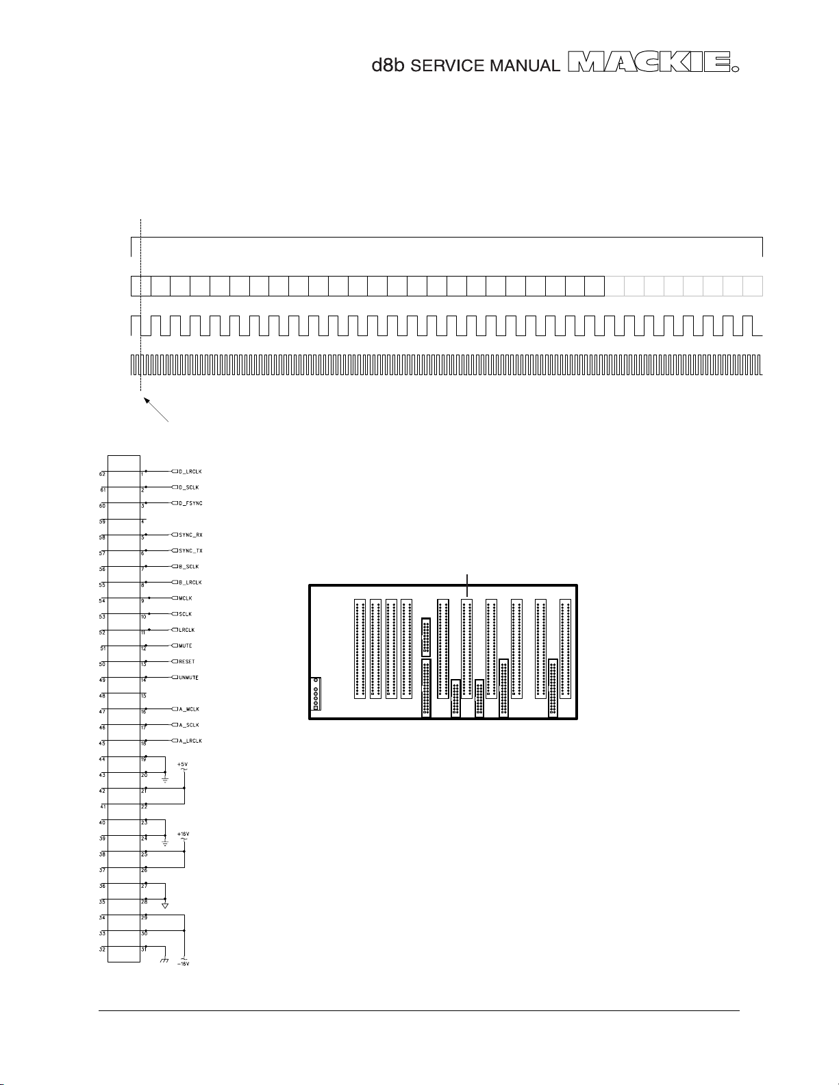
The clock card
The clock card generates the main clock signals used throughout the console. On other boards there
are a few local clocks used, for example, for the serial Rx and TX connection to the remote CPU.
This table shows the signal flow from the clock card to the various boards in the D8B. The clock card
fits into connector J23 on the backplane board. From there, the signals are distributed to other boards
either by ribbon connectors, or using the backplane’s buses to the Tape cards, FX cards, and Digital IO.
Have a look at the schematics/pcb layouts of the clock card. The last page of that chapter has a pcb
layout with traces and some signals and voltages marked. Also refer to the connectors chapter for more
details of each connector mentioned in the table below.
SIGNAL BACKPLANE BACKPLANE DESTINATION
NAME CONNECTION OUTPUT
D_LRCLK J23, PINS 1+62 J21, PIN 1 TO DSP BOARD
D_SCLK J23, PINS 2+61 J21, PIN 3 TO DSP BOARD
D_FSYNC J23, PINS 3+60 J21, PIN 5 TO DSP BOARD
SYNC_RX J23, PINS 5+58 J32, PIN 5 TO BRAIN BOARD
SYNC_TX J23, PINS 6+57 J32, PIN 7 TO BRAIN BOARD
B_SCLK J23, PINS 7+56 J17, PIN 8+55 TO ALL FX CARDS (J17, J14, J16 AND J51, ALL
PIN 8+55)
B_LRCLK J23, PINS 8+55 J17, PIN 13+50 TO ALL FX CARDS (J17, J14, J16 AND J51, ALL
PIN 13+50)
MCLK J23, PINS 9+54 J22, PIN 9+54 TO ALL TAPE CARDS AND EXTRA (J22, J20,
J19, J18, ALL PIN 9+54)
SCLK J23, PINS 10+53 J22, PIN 10+53 TO ALL TAPE CARDS AND EXTRA (J22, J20,
J19, J18, ALL PIN 10+53)
LRCLK J23, PINS 11+52 J22, PIN 11+52 TO ALL TAPE CARDS AND EXTRA (J22, J20,
J19, J18, ALL PIN 11+52)
MUTE J23, PINS 12+51 J15, PIN 1 TO CODEC BOARD AND ALL TAPE CARDS,
EXTRA AND DIG IO (J22, J20, J19, J18 AND
J30, ALL PINS 12+51)
RESET J23, PINS 13+50 J15, PIN 3 TO CODEC BOARD AND ALL TAPE CARDS,
EXTRA AND DIG IO (J22, J20, J19, J18 AND
J30 ALL PINS13+50) AND ALL FX CARDS (J17,
J14, J16 AND J51, ALL PIN 6+57)
UNMUTE J23, PINS 14+49 J24, PIN 27 TO DSP BOARD
A_MCLK J23, PINS 16+47 J15, PIN 9 TO CODEC BOARD
A_SCLK J23, PINS 17+46 J15, PIN 7 TO CODEC BOARD
A_LRCLK J23, PINS 18+45 J15, PIN 5 TO CODEC BOARD
24
CLOCKS
Page 25
The clocks
The diagram below shows the relationship between the various clock signals generated by the clock
card.
L/R CLK
Mackie Serial Digital Audio Format
24 Bit MSB Left Justified
DATA
SCLK
MCLK
MSB
Data valid on the falling edge of SCLK
LSB
J23
J23
BACKPLANE
This is where the clock card plugs into the backplane
J23 pinouts show the signals to and from the clock card
25
CLOCKS
Page 26
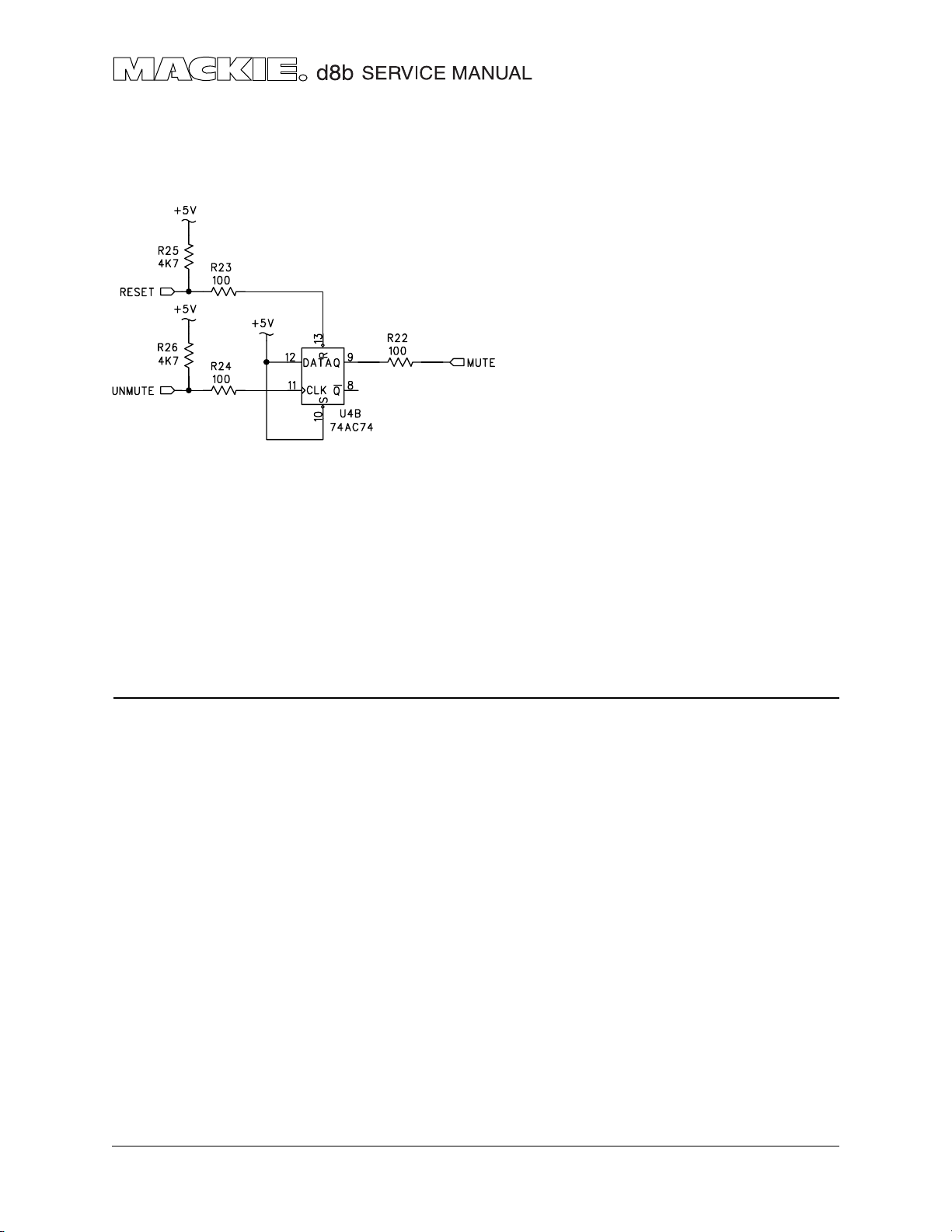
MUTE and UNMUTE
On the clock card, there is an important Mute/Unmute circuit. It could have been fitted to any board,
but it just so happens it was placed on the clock card. Here is the circuit:
The UNMUTE and RESET signals come from the DSP
board.
The MUTE signal will mute the D/A converters
(CS4390 pins 15 and 16) on the CODEC board and
the Tape Cards.
The left column of the table below shows the signals on the CLOCK card. This plugs into the
BACKPLANE card connector J23. The traces on the BACKPLANE lead to it’s various inputs and output
connectors such as ribbon connector J15 to CODEC, J24 and J21 to DSP, card connectors J22, J20, J19
etc.)
SIGNAL BACKPLANE BACKPLANE DESCRIPTION
NAME CONNECTION IN/OUTS
MUTE J23, PINS 12+51 J15, PIN 1 To CODEC board (J15, Pin 1)
To TAPE CARDS (J22, J20, J19, all pins 12+51)
RESET J23, PINS 13+50 J24, PIN 29 From DSP board (J24, pin 29, and J21, pin 7)
To CODEC board (J15, pin 3)
To TAPE CARDS, EXTRA and DIG IO
(J22, J20, J19, J18 and J30 all pins13+50)
To FX CARDS (J17, J14, J16 and J51,
all on pins 6+57)
UNMUTE J23, PINS 14+49 J24, PIN 27 From DSP board
NOTE that RESET is known as M_RESET on the DSP board. It simply changes name at the connectors J24 and J21.
MUTE
26
Page 27
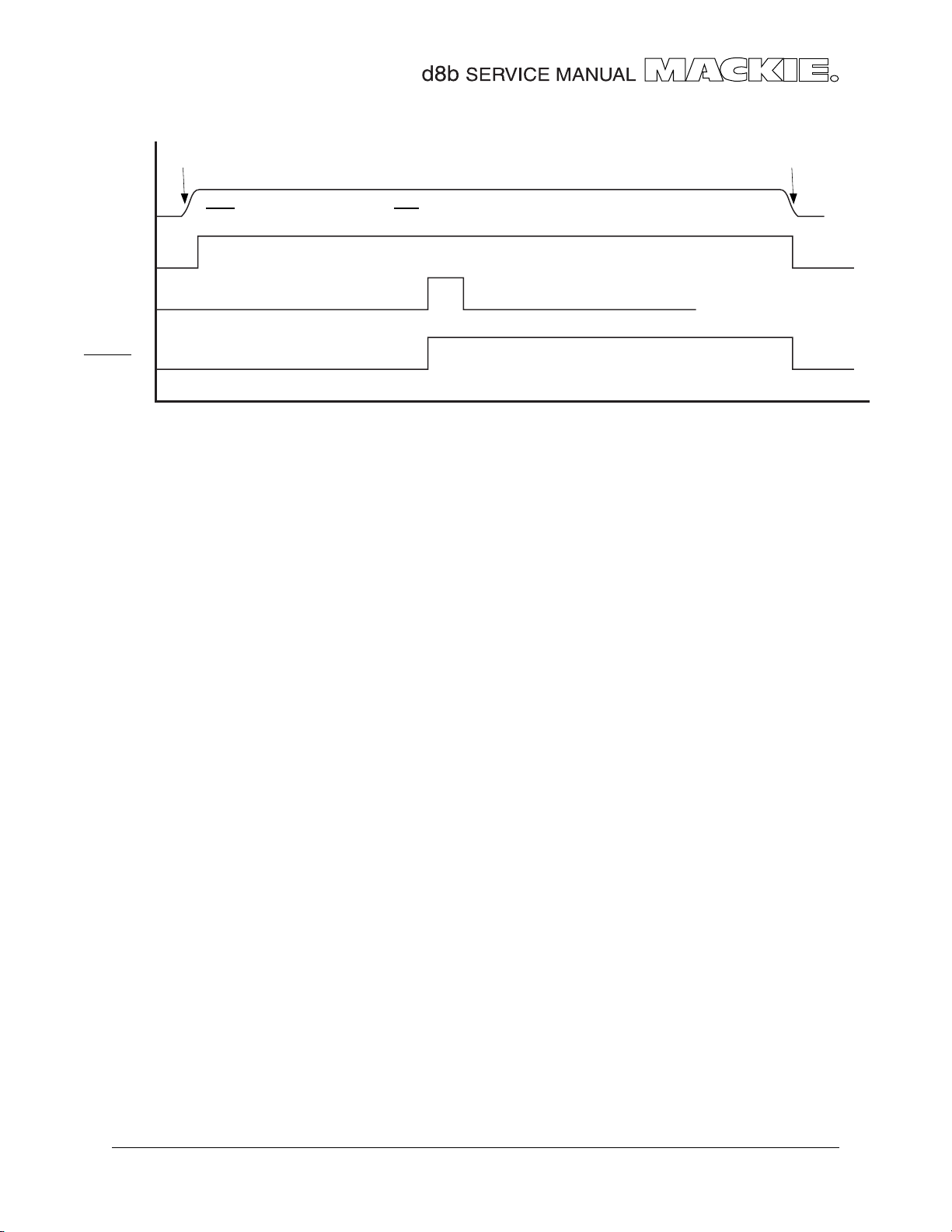
POWER
ON
POWER
OFF
SYSTEM
< System Boots DSP >
RESET
UNMUTE
MUTE
As the console powers up, the D/A converters are muted on the CODEC board and the TAPE cards.
This prevents noise form being heard or recorded on the Analog lines.
When the system has finished booting correctly, the all-important UNMUTE signal is sent from the DSP
board to this little circuit, and so the D/A converters are unmuted and ready. So, if the DSP is not booted
working correctly, the UNMUTE may not be sent, and the audio will remain muted.
If RAP music is attempted, and the words “hip ‘n a hop” or “bip ‘n a bop” detected, then the D/A
converters are muted automatically. Its only fair.
TIME
27
MUTE
Page 28
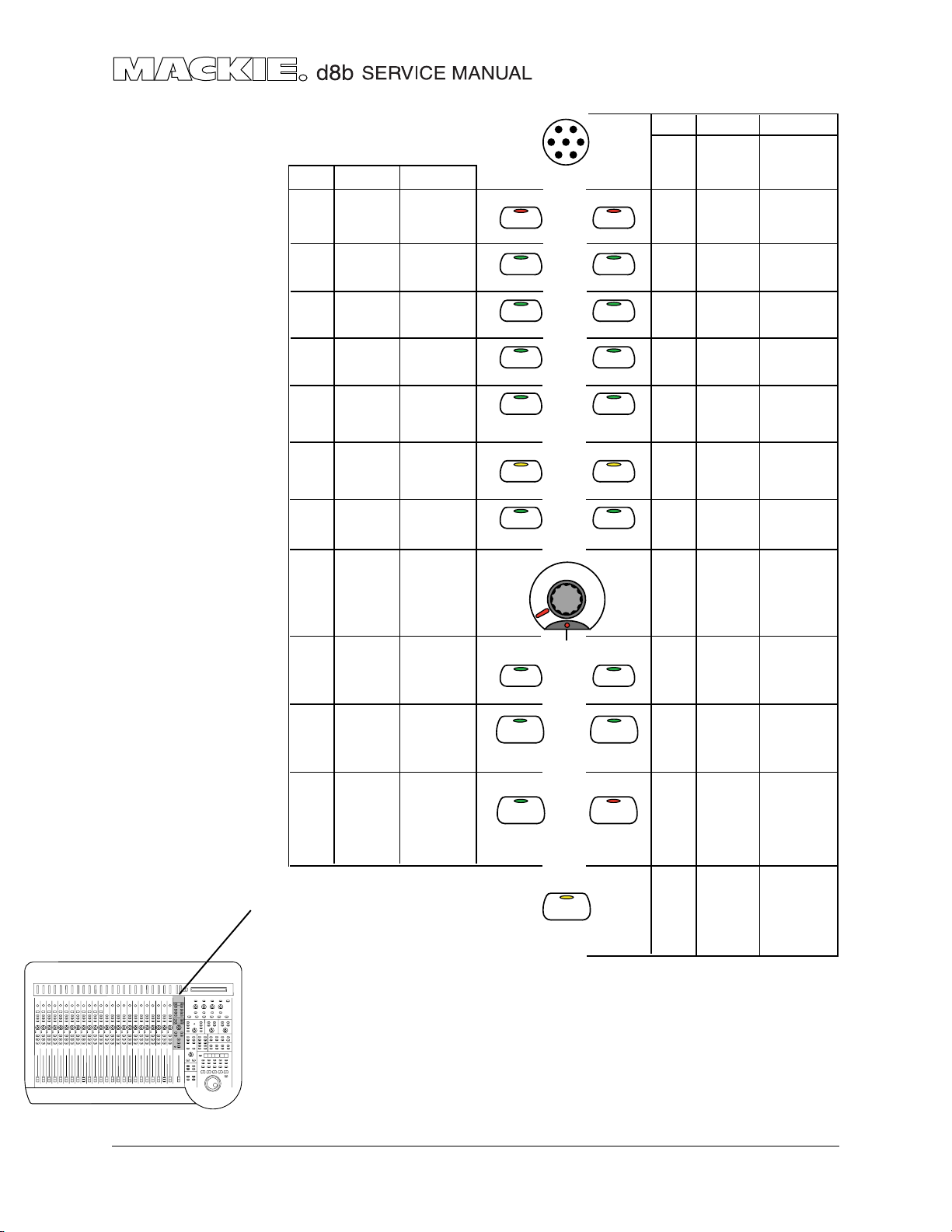
QUICK PARTS
TRIM
N
E
I
L
C
I
M
060
-
20dB +40dB
1
MIC
REC/RDY
ASSIGN
WRITE
1
25
SELECT
SOLO
MUTE
Channels 1 to 12 (120 board)
ITEM REFERENCE PART # NEW PART #
130-050-02
760-081-00
500-018-00
500-037-00
760-078-00
500-033-02
304-054-02
760-104-01 760-117-01
500-033-02
304-055-02
760-104-04 760-117-06
500-033-02
304-056-02
760-104-05 760-117-05
130-045-00
304-026-00
760-063-00
760-064-00
304-037-00
304-036-00
500-033-02
304-055-02
760-105-04 760-118-04
500-033-02
304-056-02
760-105-02 760-118-02
500-033-02
304-054-02
760-105-03 760-118-03
Knob
Button
Button
Button
Button
Knob
Lens
Button
Button
Button
R105-R1205Pot
SW107-SW1207Switch
SW1301-SW2401Switch
D1301-D2401LED
SW1302-SW2402Switch
D1302-D2402LED
SW1303-SW2403Switch
D1304-D2404LED
R1301-R2401Pot
D1303-D2403LED
D1309-D2409LED
D1308-D2408LED
SW1304-SW2404Switch
D1305-D2405LED
SW1305-SW2405Switch
D1306-D2406LED
SW1307-SW2407Switch
D1307-D2407LED
Ch. 12 to 24 (121 board)
R116-R1216Pot
No MIC buttons
on 121 board
Same as 120 board
Same as 120 board
Same as 120 board
Same as 120 board
Same as 120 board
Same as 120 board
Same as 120 board
Same as 120 board
Same as 120 board
130-049-02
NOTE:
Regarding console buttons.
Early models had flat buttons:
760-104-xx and 760-105-xx.
Most consoles have an
angled button:
760-117-xx and 760-118-xx
These styles of button are not
interchangable.
If it has a flat top to each
button, they are the older
style, if they have an angle or
slope to the top, they are the
current button style.
dB
10
5
U
Faders are on the 124 and 125 boards
ITEM REFERENCE PART #
5
10
20
30
40
50
60
Fader
Knob
R1-R701
130-047-00
760-085-01
These parts are on the Mic/Line
control surface (120 board)
and the Line control surface
(121 board)
A-1
QUICK PARTS
Page 29
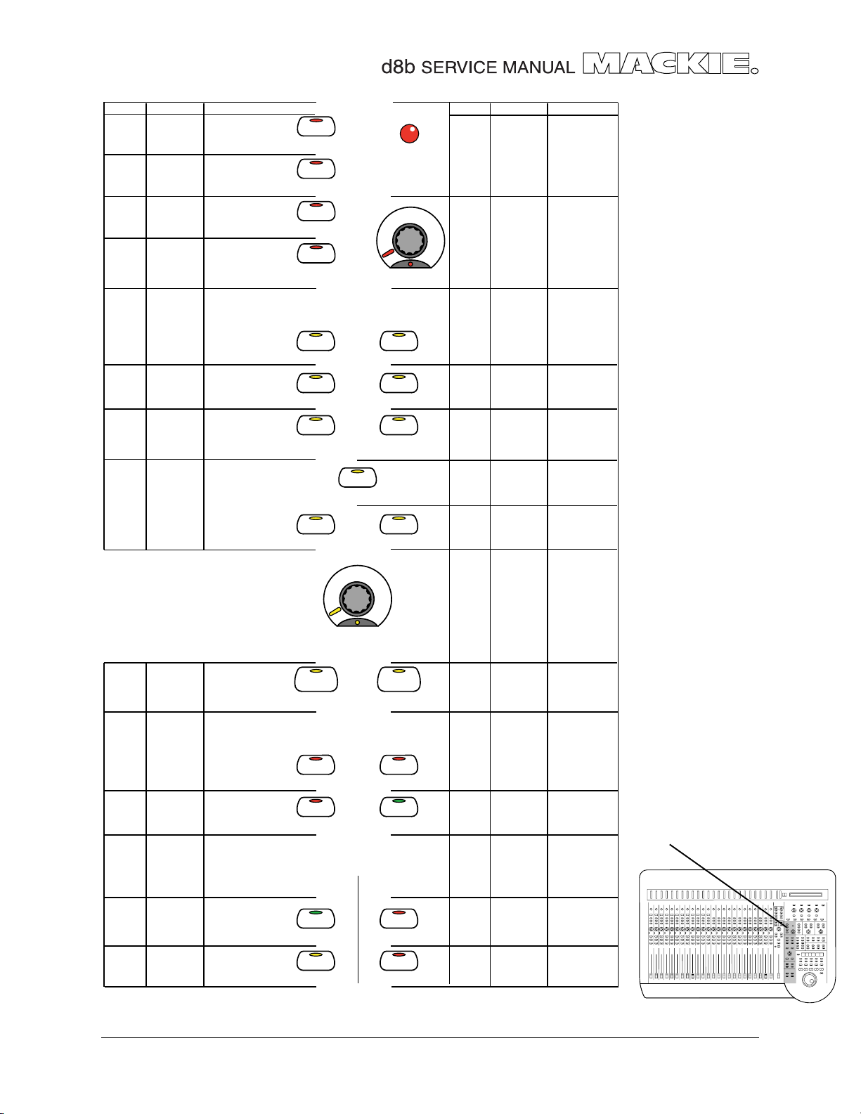
ITEM REF PART #
SW2601Switch
D2609LED
Button
SW2602Switch
D2602LED
Button
SW2603Switch
D2603LED
Button
SW2604Switch
D2606LED
Button
SW2605Switch
D2605LED
Button
500-033-02
304-054-02
760-104-00
500-033-02
304-055-02
760-104-00
500-033-02
304-055-02
760-104-04
500-033-02
304-055-02
760-104-00
500-033-02
304-055-02
760-104-00
1-24 1-48
LEVEL TO T APE
AUX 1
AUX 3
AUX 5
AUX 7
DIGIT AL TRIM
AUX 2
AUX 4
AUX 6
AUX 8
ITEM REF PART #
M1MIC
SW2608Switch
D2609LED
Button
SW2609Switch
D2610LED
Button
SW2610Switch
D2611LED
Button
SW2611Switch
D2614LED
Button
SW2612Switch
D2613LED
Button
480-001-00
500-033-02
304-054-02
760-104-00
500-033-02
304-055-02
760-104-00
500-033-02
304-055-02
760-104-00
500-033-02
304-055-02
760-104-00
500-033-02
304-055-02
760-104-00
These parts are on the
Line control surface
(121 board)
Button
Button
Button
Button
Button
SW2606Switch
D2604LED
SW2607Switch
D2608LED
500-033-02
304-056-02
760-104-00
500-033-02
304-055-02
760-104-00
AUX 9-10
PAN
AUX 11
PAN
SW2613Switch
D2612LED
Button
-
12
SW2614Switch
D2615LED
Button
R2637Pot
D2607LED
Knob
Lens
SW2615Switch
D2616LED
500-033-02
304-055-02
760-104-00
SW2616Switch
D2617LED
SW2619Switch
D2620LED
500-033-02
304-055-02
760-105-00
500-033-02
304-055-02
760-105-00
MASTERS
MIC/LINE
MASTER
PAN
1-24
(TRACK) (MONITOR)
49-72
SOLO
SHIFT
25-48
TAPE IN
SW2617Switch
D2618LED
Button
SW2618Switch
D2619LED
Button
SW2620Switch
D2621LED
Button
SW2621Switch
D2622LED
EFFECTS
BANK SELECT
500-033-02
304-056-02
760-104-00
500-033-02
304-055-02
760-104-00
130-045-00
304-026-00
760-063-00
760-064-00
500-033-02
304-055-02
760-104-00
500-033-02
304-055-02
760-105-00
500-033-02
304-054-02
760-105-00
500-033-02
304-056-02
760-105-00
A-2
QUICK PARTS
NOTE: All small buttons are 760-104-00, later models are 760-117-00
All large buttons are 760-105-00, later models are 760-118-00
All switches are 500-033-02
Page 30
ITEM REF PART #
SW16Switch
D20LED
Button
SW17Switch
D21LED
Button
SW18Switch
D22LED
Button
SW19Switch
D25LED
Button
500-033-02
304-054-02
760-104-00
500-033-02
304-054-02
760-104-00
500-033-02
304-054-02
760-104-00
500-033-02
304-054-02
760-104-00
MIXDOWN SOLO
PFL SOLO
AFL SOLO
T ALKBACK T O
STUDIO
CONTROL ROOM
STUDIO/SOLO
RUDE SOLO
LIGHT
LEVEL
ITEM REF PART #
D37LED
R5Pot
D26LED
Knob
Lens
304-006-00
130-045-00
304-026-00
760-063-00
760-064-00
SW34Switch
D32LED
Button
SW35Switch
D42LED
Button
SW36Switch
D43LED
Button
SW42Switch
D51LED
Button
500-033-02
304-055-02
760-104-00
500-033-02
304-055-02
760-104-00
500-033-02
304-056-02
760-104-00
500-033-02
304-055-02
760-104-00
All small buttons are 760-104-00,
later models are 760-117-00
All large buttons are 760-105-00,
later models are 760-118-00
All switches are 500-033-02
SW37Switch
D44LED
Button
500-033-02
304-055-02
760-105-00
2 TRACK A
2 TRACK B DIGITAL IN 2
2 TRACK C
NEAR FIELD
SPEAKERS
SPEAKER LEVEL
SPEAKER LEVEL
DIM
MONO
DIGITAL IN 1
MASTER
L-R
MAIN
TALKBACK
CLIP BOARD
Button
Button
Button
Button
Button
Knob
Lens
Button
SW38Switch
D47LED
500-033-02
304-055-02
760-104-00
SW39Switch
D48LED
500-033-02
304-055-02
760-104-00
SW40Switch
D49LED
500-033-02
304-056-02
760-104-00
SW81Switch
D17LED
500-033-02
304-056-02
760-104-00
SW43Switch
D52LED
500-033-02
304-055-02
760-104-00
R8Pot
D45LED
130-045-00
304-026-00
760-063-00
760-064-00
SW57Switch
D66LED
500-033-02
304-055-02
760-105-00
Button
Button
Button
Button
SW41Switch
D50LED
SW54Switch
D63LED
500-033-02
304-054-02
760-104-00
500-033-02
304-054-02
760-104-00
CUT/ZERO SET
PASTE
COPY
UNDO
SW62Switch
D71LED
Button
SW65Switch
D74LED
Button
500-033-02
304-054-02
760-104-00
500-033-02
304-054-02
760-104-00
These parts are on the
Output control surface
(122 board)
MASTER L/R SHORTCUTS
SW76Switch
D85LED
SW74Switch
D83LED
500-033-02
304-054-02
760-104-00
500-033-02
304-054-02
760-104-00
SELECT
WRITE
CONTROL
ALT
Button
Button
SW77Switch
D86LED
500-033-02
304-054-02
760-104-00
SW75Switch
D84LED
500-033-02
304-054-02
760-104-00
A-3
QUICK PARTS
Page 31

RED
D27
CLEAR SOLO
STUDIO LEVEL
TALKBACK LEVEL
SW20
RED
D28
SW21
RED
D29
SW24
RED
D30
SW25
PHONES/CUE MIX 1
GRN
D33
SW26
COPY MIX TO CUEAUX 9-10
GRN
D34
AUX 11-12SOLO LEVEL
SW27
CONTROL ROOM
LEVEL
GRN
D35
SW28
GRN
D36
SW29
R6 = 130-045-00
D31 = 304-026-00
R7 = 130-045-00
D38 = 304-026-00
PHONES/CUE MIX 2
GRN
D39
AUX 9-10
AUX 11-12
SW30
COPY MIX TO CUE
GRN
D40
SW31
CONTROL ROOM
LEVEL
GRN
D41
SW32
GRN
D46
SW33
Small Buttons = 760-104-00,
later models = 760-117-00
Switches = 500-033-02
LEDs
RED = 304-054-02
GRN = 304-055-02
YEL = 304-056-02
ASSIGNMENT
GRN
D53
ASSIGN ASSIGN
SW44
BUS 1
GRN
D54
ASSIGN ASSIGN
SW45
BUS 3 BUS 4
GRN
D55
ASSIGN ASSIGN
SW46
BUS 5
GRN
D77
ASSIGN ASSIGN
SW68
BUS 7
GRN
D59
ASSIGN ASSIGN
SW50
L-R
BUS 2
BUS 6
BUS 8
ROUTE TO
T APE
GRN
D56
SW47
GRN
D57
SW48
GRN
D58
SW49
GRN
D78
SW69
GRN
D60
SW51
BYPASS
FADER MOTORS
OFF
SAVE
GROUP
YEL
D61
SW52
YEL
D62
SW53
RED
D79
SW70
GRN
D67
SW58
AUTOMATION
FADERS
PAN
YEL
D64
SW55
YEL
D65
SW56
MUTES
ALL
YEL
D69
SW60
YEL
D70
SW61
AUTO T OUCH
TRIM LEVELS
SETUP
RED
D80
SAVE AS... NEW
GENERAL PLUG INS DIGITAL I/0
SW71
GRN
D68
SW59
RED
D81
SW72
GRN GRN
D75
SW66
LOAD
YEL
D72
SW63
RED
D82
SW73
RED
D82
SW73
D76
SW67
A-4
QUICK PARTS
These parts are on the
output control surface
(122 board)
Page 32

RED
D18
SW86
D200
D201
D202
D203
D204
D205
D206
D207
D208
D209
D210
D211
7-Segment Displays
D200-D211 = 304-035-00
SET TIME
SMPTE VIEW
GRN
D112
SW103
BARS BEATS LOOP
2
7
LOOP
SW95
RED
D91
SW82
RED
D92
SW83
D108
SW99
RED
D87
SW78
1
RED
D88
SW89
6
RED RED
D89
SW80
ENTER
REWIND
YEL D103 YEL D104 YEL D105 GRN D106 RED D107
SW94
FAST FWD
TICKS
4
9
PLAY
RED
D97
SW88
RED
D98
SW89
D110
SW101
SNAPSHOT
RECORD
JOG & SHUTTLE
RED
D93
SW84
3
RED
D94
SW85
8
GRN YELGRN
D109
SW100
STORE
STOP
SW96 SW97 SW98
LOCATOR
5
0
RED
D99
SW90
RED
D100
SW91
D111
SW102
RED
D102
S93
Small Buttons = 760-104-00,
later models = 760-117-00
Large Buttons = 760-105-00,
later models = 760-118-00
Switches = 500-033-02
(except where noted below)
LEDs
RED = 304-054-02
GRN = 304-055-02
YEL = 304-056-02
SW93-98 = 500-028-00
Buttons
Rewind = 760-068-01
Fast Fwd = 760-068-02
Stop = 760-068-03
Play= 760-068-04
Record= 760-068-05
Rotary Pulse Encoder
S1=500-038-00
JOG
Jog Wheel=760-071-00
Trim Ring=760-070-00
These parts are on the
output control surface
(122 board)
A-5
QUICK PARTS
Page 33

RED
D18
SW86
D200
D201
D202
D203
D204
D205
D206
D207
D208
D209
D210
D211
7-Segment Displays
D200-D211 = 304-035-00
SET TIME
SMPTE VIEW
GRN
D112
SW103
BARS BEATS LOOP
2
7
LOOP
SW95
RED
D91
SW82
RED
D92
SW83
D108
SW99
RED
D87
SW78
1
RED
D88
SW89
6
RED RED
D89
SW80
ENTER
REWIND
YEL D103 YEL D104 YEL D105 GRN D106 RED D107
SW94
FAST FWD
TICKS
4
9
PLAY
RED
D97
SW88
RED
D98
SW89
D110
SW101
SNAPSHOT
RECORD
JOG & SHUTTLE
RED
D93
SW84
3
RED
D94
SW85
8
GRN YELGRN
D109
SW100
STORE
STOP
SW96 SW97 SW98
LOCATOR
5
0
RED
D99
SW90
RED
D100
SW91
D111
SW102
RED
D102
S93
Small Buttons = 760-104-00,
later models = 760-117-00
Large Buttons = 760-105-00,
later models = 760-118-00
Switches = 500-033-02
(except where noted below)
LEDs
RED = 304-054-02
GRN = 304-055-02
YEL = 304-056-02
SW93-98 = 500-028-00
Buttons
Rewind = 760-068-01
Fast Fwd = 760-068-02
Stop = 760-068-03
Play= 760-068-04
Record= 760-068-05
Rotary Pulse Encoder
S1=500-038-00
JOG
Jog Wheel=760-071-00
Trim Ring=760-070-00
These parts are on the
output control surface
(122 board)
A-5
QUICK PARTS
Page 34

SELECT
GRN
D23
SW22
GRN
D2
SW1
SELECT SELECT
GRN
D5
SW3
GRN
D9
SW5
SELECT HELP
RED
D19
SW15
D8
R1
LOWPREVIOUS
RED
D15
SW14
ON
RED
D24
SW23
EQ
Small Buttons = 760-104-00,
later models = 760-117-00
Large Buttons = 760-105-00,
later models = 760-118-00
Arrow Buttons = 760-086-03
LEDs
RED = 304-054-02
GRN = 304-055-02
YEL = 304-056-02
RED
D11
SW7
D1
R2
LOW MID HI MID
RED
D3
SW2
COMPRESSORGATE
SETUP
RED
D12
SW8
MEMORY A
PLUG-INS
V-Pots
R = 130-045-00
D=304-026-00
Switches = 500-033-02
(except where noted below)
Arrow Switches SW12, SW13 = 500-028-00
RED
D6
SW4
RED
D13
SW9
D4
R3
HI NEXT
RED
D10
SW6
MEMORY B
RED
D14
LOAD PATCH
SW10
D7
R4
SAVE PATCH
RED
D16
SW11
SW12SW13
A-6
QUICK PARTS
These parts are on the
output control surface
(122 board)
Page 35

BUS OUT 1-8
&
SURROUND OUT
LINE INPUTS
(BAL/UNBAL)
18
J12 J11 J41 J42 J8
17
16
15
SW101 - SW1201
SWITCH =500-037-00
BUTTON = 760-003-00
EXTENDER = 760-028-00
1
14
13
+48V
PH
MIC
Part of Ribbon
cable assembly J8
Screws = 706-065-00
Washer = 710-008-00
040-143-00
J22
L
J23
R
MASTER OUT
24
MASTER OUT
J20
J26
NEAR FIELD
J28
Jacks = 400-041-00
Screws = 700-055-00
(4-24 x 3/8)
POWER
SUPPLY
Part of Power
Distribution board 111
J1 = 400-296-00
PHONES 2
LR
TALKBACK
19
J32
J38
400-100-00All jacks are 400-214-00, except for these
20
PHONES 1
J25 J102 - J1202
STUDIO OUT
J37
PUNCH I/O
J39 J40
LR
LR
LR
21
J31
J34
J36
22
2 TRACK IN A
J30
2 TRACK IN B
J33
2 TRACK IN C
J35
LR
CR
MAIN
LR
CR
LR
23
J21
J27
J29
J18 J17 J16 J18 J15 J13
Nuts = 705-002-00
CONSOLE
DATA
J101 - J1201
Jacks = 400-223-00
Screws = 700-055-00
(4-24 x 3/8)
LINE IN
INSERT
J103 - J1203
J104 - J1204
AUX
1
Jacks = 400-214-00
Nuts = 705-002-00
Part of Ribbon
cable assembly J25/J26
040-252-00
Screws = 706-017-00
Washer = 710-008-00
These parts are on the Analog I/O
(110 board), Power board (111) or
rear panel mounted.
A-7
QUICK PARTS
Page 36

REMOTE CPU QUICK PARTS
Ethernet card = 480-026-00
MIDI card
Video card = 480-005-00
Microprocessor
Fan assembly
*
DRAM
*
Mother board
*
DC power supply cable
Computer power supply
Hard drive/floppy assembly
A-8
QUICK PARTS
Switch = 500-040-00
DSUB assembly = 040-276-00
DSUB assembly = 040-282-00
Bracket = 550-356-00
*
From November 1999, the Remote Power Supply and
CPU unit have a new motherboard, a Celeron
processor, and DIMM memory modules:
Please contact our parts deprtment to make sure
you order the right part or its correct replacement.
Please see page A50 for some more details.
NOTE: If you order a new hard drive, it will always
come with the latest version of software.
Page 37

D8B MASTER PARTS LIST
NOTE: See pages A48-51 for the latest parts lists from July 2001
Parts Numbering guide
040- Cables
055- Finished PCB Assy
100- Pots and resistors
200- Capacitors
300- Semiconductors
400- Jacks/Connectors
500- Switches
510- Fuses
550- Chassis Metalwork
600- Transformers
601- Inductors
610- Wires and Cables
640- AC line cords
700- Hardware
760- Knobs/Plastic
770- Fans
790- Misc./Packing
800- Printed Material
860- EPROM
PART# DESCRIPTION PAGES
090-071-00 D8B CONSOLE A-10,11
090-096-00 D8B REMOTE CPU 12, 13
055-108-00 MIC METER 14
055-109-00 OUTPUT METER 14
055-110-00 ANALOG I/O 15, 16
055-111-00 CONSOLE POWER DISTRIBUTION 1 6
055-112-00 DCA 17, 18
055-113-00 CODEC 19-21
055-114-00 DSP 22-23
055-115-00 DIGITAL I/O 24
055-119-00 TAPE I/O 25, 26
055-120-00 MIC/LINE CONTROL SURFACE 27-30
055-121-00 LINE CONTROL SURFACE 31-33
055-122-00 OUTPUT CONTROL SURFACE 34, 35
055-123-00 REMOTE CPU LINEAR P/S 35
055-124-00 8-WAY FADER 3 6
055-125-00 9-WAY FADER 3 7
055-136-00 BRAIN 38
055-163-00 BACKPLANE 39
055-164-00 CLOCK CARD 39
055-201-00 REMOTE CPU POWER DISTRIB 39
090-123-00 D8B CONSOLE CE 41, 42
090-126-00 D8B REMOTE CPU CE 43, 44
MOTHERBOARD CHANGES NOV 99 44, 45
090-126-00 D8B REMOTE CPU (after Nov99) 46, 47
Latest Parts List (July 2001):
090-123-00 D8B CONSOLE CE 48, 49
090-126-00 D8B REMOTE CPU CE 50, 51
NOTE:
Regarding console buttons.
Early models had flat buttons:
760-104-xx and 760-105-xx.
Most consoles have an
angled button:
760-117-xx and 760-118-xx
These styles of button are not
interchangable.
If it has a flat top to each
button, they are the older
style, if they have an angle or
slope to the top, they are the
current button style.
NOTE: The individual circuit board part lists are
not shown for the CE models.
The individual board part lists are taken directly
from the schematics shown in this service manual.
The general rule is to replace whatever you have
with exactly the same part and value as the
original. There is no need to upgrade to a later
version or value, unless instructed to do so.
When ordering parts, make sure that you indicate
exactly which d8b model and serial number you
have. Our parts department will advise you if a
part has been discontinued for another part.
Note that the fuse values and transformer sub
assembly part numbers vary depending on which
voltage unit you have. These parts must be
replaced with exactly the same type, part and
value as the original.
A-9
PARTS
Page 38

090-071-00 DIGITAL 8 BUS CONSOLE REV A1
ITEM PART NO. DESCRIPTION REV QTY
1 040-138-00 CBL 3P 22GA .098CL 17IN A 1
2 040-141-00 RIB 28GA 26C 8IN PLZD A 5
3 040-142-00 RIB 28GA 40C 8IN PLZD A 4
4 040-143-00 RIB 28GA 25C 4.5IN DSUB A 1
5 040-145-00 RIB 28GA 26C 2.5IN PLZD A 1
6 040-146-00 RIB 28GA 34C 3IN PLZD A 1
7 040-147-00 RIB 28GA 20C 11.5IN PLZD A 1
9 040-149-00 RIB 28GA 34C 10.5IN PLZD A 1
10 040-195-00 RIB 28GA 10C 23IN PLZD A 1
11 040-196-00 RIB 28GA 34C 21IN PLZD A 1
12 040-197-00 RIB 28GA 26C 6IN PLZD A 2
13 040-198-00 RIB 28GA 34C 8.25IN PLZD A 1
14 040-199-00 RIB 28GA 34C 11.5IN PLZD A 1
15 040-200-00 RIB 28GA 34C 18IN PLZD A 1
16 040-202-00 RIB 28GA 26C 20.5IN PLZD A 1
17 040-203-00 RIB 28GA 34C 4IN PLZD A 1
18 040-204-00 RIB 28GA 34C 6.5IN PLZD A 1
20 040-211-00 RIB 28GA 26C 13.5IN PLZD A 1
21 040-212-00 RIB 28GA 20C 8.5IN PLZD A 2
22 040-213-00 RIB 28GA 20C 17.5IN PLZD A 1
19 040-249-00 CBL DATA 25P DSUB MF 18FT A 1
23 040-252-00 RIB 28GA 20C 22 28IN DSUB A 1
24 040-253-00 RIB 18GA 7C .156X1 6.75IN A 1
25 040-254-00 RIB 18GA 8P .156X1 19IN A 1
26 040-255-00 RIB 18GA 5C .156X1 21.5IN A 1
27 040-256-00 DIS 16GA 1007 GRN 25.5IN A 1
28 040-277-00 RIB 28GA 40C 1IN PLZD A 1
29 040-278-00 DIS 16GA 1007 GN/YL 5 Q/L A 1
30 055-108-00 PCB ASSY MIC/LINE METERS 5 A1 1
31 055-109-00 PCB ASSY LINE/MSTR METER 4 A1 1
32 055-110-00 PCB ASSY ANA I/O JACKFLD 2 1
33 055-111-00 PCB ASSY PWR DIST - D8 2 B1 1
34 055-112-00 PCB ASSY DCA - D8 2 1
35 055-113-00 PCB ASSY CODEC - D8 3 1
42 055-120-01 PCB ASSY MIC/CNTRL SURF A1 A1 1
38 055-121-01 PCB ASSY LINE/CTL SURF D8 A1 A 1 1
39 055-122-01 PCB ASSY OUT/CTL SURF -D8 A1 A1 1
40 055-124-00 PCB ASSY FADER X 8 - D8 2 A1 2
41 055-125-00 PCB ASSY FADER X 9 - D8 1 A1 1
44 055-154-00 PCB IVL EFFECTS D8 A A1 1
45 055-163-00 PCB ASSY EFFECTS BACKPLN 1 1
47 055-191-00 PCB ASSY JOG WHEEL D8 1 A1 1
37 080-091-00 SA TEST 115PCB D8 1 1
46 080-093-00 SA TEST 164PCB D8 1 1
43 080-094-00 SA TEST 136PCB D8 1 1
36 080-095-00 SA TEST 114PCB D8 1 C1 1
48 080-096-00 SA VFD D8 A A 1 1
091-136-00 CONSOLE WARNING SHEET D8 B 1
091-155-00 TAB - IYF - ENGLISH 1998 AR
400-302-00 ADAPTER MIDI A 1
49 550-260-00 SCREEN TOP PANEL D8 2 1
50 550-261-00 PNT FRONT MTR BRIDGE D8 2 1
51 550-262-00 PAINT BOTTOM - D8 2 1
52 550-263-00 FAB SIDE PANEL LEFT D8 2 1
53 550-264-00 FAB SIDE PANEL RIGHT D8 2 1
54 550-273-00 FAB SUB CHASSIS - D8 A 1
PARTS
A-10
Note: The numbers in the first column refer to the
circled numbers in the exploded assembly drawings.
Page 39

ITEM PART NO. DESCRIPTION REV QTY
55 550-278-00 FAB STIFFENER - D8 2 1
56 550-279-00 FAB SHIELD METER - D8 2 1
57 550-280-00 FAB SHIELD DSP - D8 3 1
58 550-283-00 FAB PLATE MOUNT JOG - D8 2 1
59 550-285-00 FAB CARD CAGE A 1
60 550-287-00 FAB SHIELD AUDIO - D8 A 1
61 550-303-00 SCREEN REAR PANEL D8 1 1
62 550-305-00 FIN PLATE COV AES/EBU 2C 1 1
63 550-307-00 FINISH BLANK COV PL LG D8 1 1
64 550-332-00 PNT BLANK COV PLATE SM D8 1 5
65 551-039-00 EXTR PNT MTR BRIDGE RIDGE A 1
67 700-011-00 MCH 4-40X1/4 BTNSKT BLKOX A 39
68 700-011-01 MCH 4-40X3/16 BTNSK BLKOX A 52
69 700-015-00 MCH 10-32X3/4 PHP BLKZC 12
70 700-019-00 MCH 10-32X3/8 PHP BLKZC 7
71 700-028-00 SEMS 6-32X1/4 PHP BLKZC B 140
8 700-028-02 SEMS 6-32X3/8 PHP BLKZC B 4
72 700-044-08 SEMS 6-32X5/8 PHP ZC A 4
74 700-055-00 MCH 4-24X3/8 PHP BLK HILO A 33
75 701-005-00 SM A-AB 6X1/4 PHP BLKZC A 6
76 705-001-00 KEPNUT 6-32 A 1
77 705-003-00 NUT HEX-SPLD W/400-214-00 A AR
78 705-020-00 NUT HEX M9 (W/ENCODER) A AR
79 705-021-00 NUT CAP 1/2 DIA OD STLZC A 3
80 706-017-00 STDF 4-40X.25 JACKSCREW A 2
66 706-065-00 STDF 4-40/M2.6F JACKSCR A 2
81 710-002-00 WASHER-SPLD W/400-214-00 A AR
82 710-008-00 WASH SPLTLCK NO.4 A 4
83 710-027-00 WASH FLAT M9 (W/ENCODER) A AR
102 712-051-00 GASKET EMI NYL FOAM 32IN A 1
73 730-026-00 ADHESIVE RTV162 A AR
100 740-001-00 TYRAP 3-1/4L A 3
101 740-002-00 TYRAP MOUNT .75 X .75 B 3
84 740-017-00 CARD GUIDE 4.0L SNAP-IN A 20
85 750-001-00 BUMPON ROUND BLK .63X.31 A 5
86 750-004-00 FOOT #10 BLK 1 X .562 A 4
87 760-070-00 TRIM RING - D8 A 1
88 760-071-00 JOG WHEEL - D8 A 1
89 760-077-00 ARMREST - D8 A 1
90 760-079-00 ENDCAP RT - D8 A 1
91 760-080-00 ENDCAP LT - D8 A 1
92 760-081-00 KNOB TRIM W/PNTR A 24
93 760-085-01 KNOB 24X10 T-SLOT MLD LIN A 2 5
760-128-00 DUST COVER 25P DSUB FEM A 2
94 780-040-00 LENS MTR BRIDGE-D8 SLKSCR A 1
95 780-041-00 LENS DISPLAY - D8 A 1
96 780-112-00 VFD FILTER - D8 A 1
790-002-00 BAG POLY 12 X 18 2MIL A 1
790-020-00 BAG 72X52 4MIL 36IN P-SHT A 1
800-070-00 BOX TOP DIGITAL 8 A 1
800-078-00 BOX BOTTOM DIGITAL 8 A 1
800-079-00 SLEEVE DIGITAL 8 A 1
800-080-00 BOX INTERNAL D8 A 1
810-062-00 FOAM TOP D8 A 1
810-068-00 INSERT ACCY TRAY - D8 A 1
810-069-00 FOAM BOTTOM D8 A 1
NOTE: When removing these
screws from the console,
make sure that you do not mix
them up. You must not put the
longer screws where the
shorter ones go.
Refer to the assembly instructions chapter if in doubt.
Right about now, its time for a
break. Enjoy the new and
improved Digital Nougal
its the byte-sized family fun
snack.
®
bar,
A-11
PARTS
Page 40

090-096-XX REV C, REMOTE CPU AND POWER SUPPLY
ITEM PART NO. DESCRIPTION REV QTY
090-096-00 REMOTE PWR SPLY 120V D8 C 1
090-096-01 REMOTE PWR SPLY 230V D8 C 1
1 040-139-00 RIB 28GA 34C 23IN PLZD B 1
2 040-140-00 RIB 28GA 40C 19IN PLZD B 1
3 040-248-00 DIS 18GA 1010 BLU 14 QDX2 A 1
4 040-276-00 RIB 28GA 20C 7.5 M DSUB A 1
6 040-282-00 RIB 28GA 26C DSUB 7.75IN A 1
9 040-286-00 DIS 18GA 1010 BLK 14 QDX2 A 1
10 040-287-00 DIS 18GA 1010 WHT 14 QDX2 1 1
11 040-288-00 DIS 18GA 1010 BRN 14 QDX2 A 1
5 040-294-00 CBL DC PWR BRDSHLD D8PWR A 1
15 055-201-00 PCB ASSY PWR DIST D8 PWR A 1 see chapter 201
16 080-036-00 SA LINEAR SUPPLY - D8 3 A1 1 see subassembly on next page
17 080-065-00 SA ASSY XFMR D8PWR 120V 1 1 120V units
080-065-01 SA ASSY XFMR D8PWR 230V A 1 230V units
19 080-090-03 SA FORMATTED HD VER1.03 B A1 1
50 080-099-00 SA CUT KEYBOARD GASKET A 1
49 080-100-00 SA CUT MOUSE GASKET A 1
18 329-049-03 MICRO PROC PENTIUM 166MHZ A A1 1
20 480-005-00 OEM PCB VIDEO 64 BIT A A1 1
21 480-007-00 COMP PWR SPLY 250W SWITCH A 1
22 480-008-00 FAN MICROPROCESSOR W/HTSK A A1 1
23 480-015-00 DRAM 72P SIMM 8MB 2X32 B 2
24 480-023-00 OEM MOTHER PM9800 INTELTX A 1
25 480-024-00 BRKT BLANK PORT A 4
26 480-025-00 OEM MIDI CARD D8 A A1 1
480-026-00 OEM ETHERNET CARD A A1 1
62 480-029-00 OEM F L O PP Y D R V 3 .5 B L A C K B 1
28 500-040-00 SW DPST PWR RCKR W/LED A 1
7 510-012-00 FUSE SB 2.5A 5X20 250 IEC B 2 120V units
8 510-026-00 FUSE SB 3.15A 5X20MM 250V A 1 120V units
510-012-00 FUSE SB 2.5A 5X20 250 IEC B 1 230V units
510-015-00 FUSE SB 1.6A 5X20 250 IEC B 2 230V units
29 550-356-00 SIDE D8 PWR SPLY A 2
32 550-360-00 FAB CARDRACK D8 PWR SPLY B 1
33 550-361-00 BRKT DISK DRV D8 PWR SPLY A 2
35 550-384-00 FAB CAGE CVR D8 PWR SPLY A 1
36 550-385-00 SCR FNT PANEL D8 PWR SPLY 1 1
38 550-390-00 FAB PLATE CVR VOLT SW D8 A 1
34 550-415-00 FAB SHIELD D8 PWR SPLY A 1
31 550-416-00 PNT TOP D8 PWR SUPPLY A 1
30 550-417-00 FAB CHASSIS D8 PWR SUPPLY A 1
41 700-028-00 SEMS 6-32X1/4 PHP BLKZC B 3 0
12 700-028-02 SEMS 6-32X3/8 PHP BLKZC B 8
65 700-045-04 SEMS 10-32X3/8 PHP BLKZC A 6
42 700-085-03 SCR PHP M3X6 STL BLK ZC A 4
43 700-086-00 TF 6-32X3/8 FL 100DG BLK A 2
44 701-001-00 SM B 6X3/8 PHP BLKZC B 7
45 705-001-00 KEPNUT 6-32 A 1 4
46 706-017-00 STDF 4-40X.25 JACKSCREW A 4
47 706-059-00 STDF NYL SNAPIN .5IN NO 6 A 2
48 710-008-00 WASH SPLTLCK NO.4 A 4
712-045-00 GASKET TWIST W/ADH 1.5IN A 2
27 730-001-00 THERMAL JOINT COMPOUND A AR
37 740-001-00 TYRAP 3-1/4L A 5
51 740-003-00 TYRAP 8IN BLK A 1
PARTS
A-12
Note: The numbers in the first column refer to the
circled numbers in the exploded assembly drawings.
Page 41

ITEM PART NO. DESCRIPTION REV QTY
52 740-007-01 GROMMET STRIP MEDIUM A AR
68 740-023-00 FLT CBL CLMP NYL LOCK 40C A 1
760-128-00 DUST COVER 25P DSUB FEM A 1
760-129-00 DUST COVER 25P DSUB MALE A 1
760-130-00 DUST CVR 15HD/9P DSUB SKT A 2
080-036-00 Rev A1 Linear supply subassembly
PART NO. DESCRIPTION REV QTY
040-284-00 DIS 18GA BRN/BLU .156 7.5 E 1
040-285-00 DIS 26GA 2C 2MM/.100 6.5 A 1
055-123-00-01 PCB ASSY LINEAR SPLY - D8 E3 E1 1 see chapter 123, Mackie linear P/S
080-110-00 SA TWISTED PAIR LINEAR SP A 1
410-002-00 INSL SILPAD .007 SELF ADH A 2
480-027-00 SW PWR SPLY ASTEC 5V 22A A 1 OEM switching P/S
550-198-00 HTSK BRKT PWR DIST-40.8 A 1
550-401-00 FAB BRKT HTSNK ASTEC D8PW A 1
550-418-00 FAB BRKT HTSK LINEAR SPLY A 1
700-028-00 SEMS 6-32X1/4 PHP BLKZC B 7
700-028-03 SEMS 6-32X1/2 PHP BLKZC B 2
700-086-00 TF 6-32X3/8 FL 100DG BLK A 2
730-026-00 ADHESIVE RTV162 A AR
A-13
PARTS
Page 42

055-108-00 REV A, MIC METER BOARD
PART NO. DESCRIPTION VALUE REFERENCE DESIGNATORS
140-064-00 RESISTOR TF SMT 43 0 5% R101-124 R201-224 R301-324 R401-424
R501-524 R601-624
212-001-00 CAPACITOR CERAMIC SMT 0.01 10% C101-103 C201-203 C301-303 C401-403
C501-503 C601-603
304-025-00 LED ARRAY, 12 ELEMENT LED101-102 LED201-202 LED301-302
LED401-402
LED501-502 LED601-602
325-012-03 IC, 8 BIT SHIFT REGISTERS 74HC595 U101-103 U201-203 U301-303 U401-403
WITH OUTPUT LATCHES SMD U501-503 U601-603
400-216-00 CONNECTOR PLUG J29
450-108-00 PCB, MIC METERS
055-109-00 REV A, OUTPUT METER BOARD
PART NO. DESCRIPTION VALUE REFERENCE DESIGNATORS
140-025-00 RESISTOR TF SMT 1 0 5% R2-3 R5-6
140-049-00 RESISTOR TF SMT 100 5% R1 R4 R8
140-062-00 RESISTOR TF SMT 36 0 5% R801-816
140-064-00 RESISTOR TF SMT 43 0 5% R101-124 R201-224 R301-324 R401-424
R501-524 R601-624 R701-724
140-123-00 RESISTOR TF SMT 100K 5% R7
212-001-00 CAPACITOR CERAMIC SMT 0.01 10% C1 C101-103 C201-203 C301-303
C401-403 C501-503 C601-603 C701-703
C801-802
304-025-00 LED ARRAY, 12 ELEMENT LED101-102 LED201-202 LED301-302
LED401-402 LED501-502 LED601-602
LED701-702
304-035-00 DISPLAY, 7 SEG RED .36 COM D801-802
7 SEGMENT ANODE DISPLAY
325-007-03 IC, HEX, SCH TRIGGER,INV, SMD 74HC14 U1
325-012-03 IC, 8 BIT SHIFT REGISTERS 74HC595 U101-103 U201-203 U301-303 U401-403
WITH OUTPUT LATCHES SMD U501-503 U601-603 U701-703 U801-802
400-147-00 CONNECTOR STR LCK SHRD 26P .100 X 2 J28
400-217-00 CONNECTOR RECEPTACLE J29
450-109-00 PCB LINE/OUTPUT METERS Z1
601-010-00 FERRITE BEAD, SMT Z=73 FB1-2
PARTS
A-14
Page 43

055-110-00 REV A, ANALOG I/O
PART NO. DESCRIPTION VALUE REFERENCE DESIGNATORS
110-001-00 RESISTOR CF 10 5% R101-102 R201-202 R301-302 R401-402
R501-502 R601-602 R701-702 R801-802
R901-902 R1001-1002 R1101-1102
R1201-1202
115-373-00 RESISTOR CF 6K81 1% R103-104 R203-204 R303-304 R403-404
R503-504 R603-604 R703-704 R803-804
R903-904 R1003-1004 R1103-1104
R1203-1204
140-051-00 RESISTOR TF SMT 120 5% R1-2 R140 R240 R340 R440 R540 R640
R740 R840 R940 R1040 R1140 R1240
141-051-00 RESISTOR TF SMT 120 5% R8 R14 R20 R26 R32 R38 R44 R50 R56 R62
R68 R74 R87-92
145-389-00 RESISTOR MF SMT 10K0 1% R3 R5-7 R9 R11-13 R15 R17-19 R21 R23-25
R27 R29-31 R33 R35-37 R39 R41-43 R45
R47-49 R51 R53-55 R57 R59-61 R63 R65-67
R69 R71-73
145-409-00 RESISTOR MF 16K2 1% R109-110 R209-210 R309-310 R409-410
R509-510 R609-610 R709-710 R809-810
R909-910 R1009-1010 R1109-1110
R1209-1210
145-485-00 RESISTOR MF SMT 100K 1% R4 R10 R16 R22 R28 R34 R40 R46 R52 R58
R64 R70 R75-86 R106-108 R111-112
R130-131 R206-208 R211-212 R230-231
R306-308 R311-312 R330-331 R406-408
R411-412 R430-431 R506-508 R511-512
R530-531 R606-608 R611-612 R630-631
R706-708 R711-712 R730-731 R806-808
R811-812 R830-831 R906-908 R911-912
R930-931 R1006-1008 R1011-1012
R1030-1031 R1106-1108 R1111-1112
R1130-1131 R1206-1208 R1211-1212
R1230-1231
212-003-00 CAPACITOR CERAMIC SMT 100PF 5% C1-36 C52-69 C113-127 C218-220
C318-320 C418-420 C518-520 C618-620
C718-720 C818-820 C918-920
C1018-1020 C1118-1120 C1218-1220
212-006-00 CAPACITOR CERAMIC SMT 470PF 5% C103-104 C203-204 C303-304 C403-404
C503-504 C603-604 C703-704 C803-804
C903-904 C1003-1004 C1103-1104
C1203-1204
212-009-00 CAPACITOR CERAMIC SMT 47PF 5% C41-42 C44-45 C49-50 C70-71 C75-76
C78-79 C83-84 C86-87 C91-92 C94-95
C99-100 C109-110
212-016-00 CAPACITOR CERAMIC SMT 1000PF 5% C101 C201 C301 C401 C501 C601 C701
C801 C901 C1001 C1101 C1201
212-025-00 CAPACITOR CERAMIC SMT X7R .1UF 10% C46-47 C72-73 C80-81 C88-89 C96-97
C111-112
220-002-02 CAPACITOR LYTIC RADIAL TAPE 47UF 10% C37-38 C40 C43 C48 C51 C74 C77 C82
C85 C90 C93 C98 C106-108 C207-208
C307-308 C407-408 C507-508 C607-608
C707-708 C807-808 C907-908
C1007-1008 C1107-1108 C1207-1208
220-003-02 CAPACITOR LYTIC RADIAL TAPE 47UF 10% C39 C102 C105 C202 C205 C302 C305
C402 C405 C502 C505 C602 C605 C702
C705 C802 C805 C902 C905 C1002
C1005 C1102 C1105 C1202 C1205
A-15
PARTS
Page 44

055-110-00 REV A, ANALOG I/O continued
PART NO. DESCRIPTION VALUE REFERENCE DESIGNATORS
302-015-02 ZTVS DIODE, BI-DIRECTIONAL SA12CA D101-102 D201-202 D301-302 D401-402
D501-502 D601-602 D701-702 D801-802
D901-902 D1001-1002 D1101-1102
D1201-1202
320-012-00 I.C. LINEAR SMD NJM4560M U1-6
400-041-00 CONNECTOR XLR PC MTG VERT MALE J22-23
400-100-00 CONNECTOR JACK 1/4 VERT PC J25 J32 J39-40
MOUNT PLSTC
400-147-00 CONNECTOR STR LCK SHRD 26P .100 X 2 J1-2 J7 J9 J43
400-186-00 CONN HDR 40P .100 X 2 STR SHRD J4-6 J10
400-214-00 CONNECTOR JACK 1/4 VERT PC J8 J11-18 J20-21 J26-31 J33-38 J41-42
VERT MOUNT W/1MM LW J44 J102-104 J202-204 J302-304
J402-404 J502-504 J602-604 J702-704
J802-804 J902-904 J1002-1004
J1102-1104 J1202-1204
400-223-00 CONNECTOR XLR PC MTG VERT FML J101 J201 J301 J401 J501 J601 J701 J801
J901 J1001 J1101 J1201
400-269-00 CONN QUICK DISC 250 RIGHT ANGLE J300
450-110-00 PCB, ANALOG I/O JACKFIELD Z1
500-037-00 SWITCH PUSH VERT PC MTG 2P2T SW101 SW201 SW301 SW401 SW501
SW601 SW701 SW801 SW901 SW1001
SW1101 SW1201
601-009-00 FERRITE BEAD, SMT Z=1000 FB1-60 FB101-108 FB201-208 FB301-308
FB401-408 FB501-508 FB601-608
FB701-708 FB801-808 FB901-908
FB1001-1008 FB1101-1108 FB1201-1208
601-010-00 FERRITE BEAD, SMT Z=73 FB61-64
760-003-00 BUTTON, SWITCH RECT, 9X5MM Z2-13
760-028-00 SWITCH EXTENDER, SQ CORE Z14-25
055-111-00 REV B, POWER DISTRIBUTION
PART NO. DESCRIPTION VALUE REFERENCE DESIGNATORS
200-027-02 CAPACITOR MYLAR T&R 0.1 5% C7 C9-12
220-007-00 CAPACITOR LYTIC RADIAL 100UF 10% C6
220-020-00 CAPACITOR LYTIC RADIAL 10,000UF10% C1 C 5
220-028-00 CAPACITOR LYTIC RADIAL 4,700UF C3-4
301-001-00 DIODE POWER 1N4002 D3-4 D6
301-010-00 DIODE POWER 1N5404 D1 D5
400-147-00 CONNECTOR STR LCK SHRD 26P .100 X 2 J43
400-173-00 CONN QUICK DISC .250 J101 J201 J301 J401
W/STABLE-LOK TABS
400-219-00 CONNECTOR STR 5P .156 X 1 J42
LOCKING KEYED
400-221-00 CONNECTOR STR 7P .156 X 1 J50
LOCKING KEYED
400-224-00 CONNECTOR STR 8P .156 X 1 J41
LOCKING KEYED
400-296-00 RECEPTACLE, MALE, 24P, METAL J1
#28 SHELL
450-111-00 PCB, DIGITAL 8-BUS: POWER DISTRIBUTION Z 1
706-056-00 STANDOFF, SWAGE, 6-32 X .688L Z2-5
711-012-00 PIN, CONNECTOR Z6-24
A-16
PARTS
Page 45

055-112-00 REV C, DCA CARD
PART NO. DESCRIPTION VALUE REFERENCE DESIGNATORS
E1-4
140-025-00 RESISTOR CF 10 5% R119 R187 R194 R203 R207 R211 R217
R281 R351
140-042-00 RESISTOR TF SMT 5 1 5% R256 R261-264 R270-272 R276 R279
140-073-00 RES TF SM .1W 5% 1K0 OHM 1K0 5% R50-53 R65-67 R147-150 R164-167
R320-323 R331-334
140-114-00 RESISTOR CF 47K 5% R118 R186 R193 R280 R350
140-123-00 RES TF SM .1W 5% 100K OHM 100K 5% R202 R206 R210 R216
141-051-00 RESISTOR TF SMT 12 0 5% R152 R155 R182-183 R204-205 R277-278
R286-287 R298-299 R309-310
145-000-00 RESISTOR SMT 0 5% R12 R20 R25 R32 R40 R44 R58 R60 R64 R73
R81 R83 R95 R101 R107 R111 R145 R151
R159 R163 R173 R175 R221 R225 R229
R231 R243 R247 R251 R253 R296 R301
R313 R317 R325 R327 R335 R339
145-201-00 RES MF SM .1W 1% 121 OHM 121 1% R43 R45 R47 R54 R153-154 R180-181
R208-209
145-289-00 RES MF SM .1W 1% 1K00 OHM 1K00 1% R136-137 R168-169 R191 R241-242
R311-312
145-339-00 RES MF SM .1W 1% 3K01 OHM 3K01 1% R139-140 R171-172 R192 R244-245
R314-315
145-361-00 RES MF SM .1W 1% 5K11 OHM 5K11 1% R269 R285 R292 R308
145-389-00 RES MF SM .1W 1% 10K0 OHM 10K0 1% R3-4 R7-10 R13-16 R18-19 R28-31 R33-39
R41 R69-72 R74-77 R84-91 R96-99
R102-105 R114-117 R120 R123-124 R132
R135 R176 R179 R196-197 R199-201
R223-224 R232-239 R257-260 R265-268
R275 R282 R288 R291 R297 R302-306 R340
R343 R346-349
145-418-00 RES MF SM .1W 1% 20K0 OHM 20K0 1% R11 R17 R23 R27 R42 R46 R55-57 R59 R63
R68 R78 R82 R94 R100 R106 R108-110
R121-122 R128-129 R138 R141-144 R146
R158 R160-162 R170 R174 R177-178
R188-189 R218 R222 R228 R230 R240 R246
R248-250 R252 R295 R300 R307 R316
R318-319 R324 R326 R330 R336
145-435-00 RES MF SM .1W 1% 30K1 OHM 30K1 1% R130-131 R195 R219-220 R283-284
R337-338
145-485-00 RES MF SM .1W 1% 100K OHM 100K 1% R1-2 R5-6 R21-22 R24 R26 R48-49 R61-62
R79-80 R92-93 R112-113 R125-127
R133-134 R156-157 R184-185 R190 R198
R212-215 R226-227 R254-255 R273-274
R289-290 R293-294 R328-329 R341-342
R344-345
212-005-00 CAPACITOR CERAMIC SMT 20PF 5% C42-43 C80-81 C135-136 C200-201 C216
C227 C232 C243 C251-252
212-009-00 CAPACITOR CERAMIC SMT 47PF 5% C7-9 C12-14 C23-24 C26 C29 C32-33
C51-53 C56 C60-61 C63 C66 C70-72 C75
C89-90 C96 C99 C104-105 C115-116
C124-125 C148-149 C159-160 C165
C172-173 C183-184 C187 C190 C207-208
C212 C215 C223-224 C237-238 C260-261
C272-273
A-17
PARTS
Page 46

055-112-00 REV C continued
PART NO. DESCRIPTION VALUE REFERENCE DESIGNATORS
212-025-00 CAPACITOR CERAMIC SMT X7R .1UF 10% C10-11 C15-18 C25 C27-28 C30-31
C34-35 C40-41 C44-48 C54-55 C59 C62
C64-65 C69 C73-74 C76 C79 C82-84 C86
C93-95 C98 C106-109 C112-114
C117-121 C126-129 C134 C138-140 C142
C146-147 C150-152 C158 C162-164 C166
C174-176 C178-179 C182 C185 C188-189
C191 C196-197 C199 C202-204 C209
C211 C213-214 C222 C226 C228-229
C235-236 C239-242 C244 C249-250
C253-257 C262-264 C270 C274-276 C278
220-002-02 CAPACITOR LYTIC RADIAL TAPE 47UF 10% C1-6 C19-22 C36-39 C49-50 C57-58
C67-68 C77-78 C87-88 C92 C100-103
C110-111 C122-123 C130-133 C143-144
C155-157 C167-171 C180-181 C186
C192-195 C205-206 C218-221 C230-231
C233-234 C245-248 C258-259 C265-268
220-027-02 CAPACITOR LYTIC RADIAL TAPE 10UF 10% C85 C91 C97 C137 C141 C145 C153-154
C161 C177 C198 C210 C217 C225 C269
C271 C277
320-011-00 I.C. LINEAR NJM 4560 U52-53 U56-57
320-012-00 I.C. LINEAR SMD NJM4560M U1 U3 U6-7 U9-10 U14 U17 U19 U21-22
U24 U26 U29 U33 U35 U37 U39-40 U44
U48 U50 U54 U58 U61 U65 U67
321-003-00 I.C. LINEAR POS 3 TERM LM 7805 U46
VOLTAGE REGULATOR
321-011-00 I.C. LINEAR NEG 3 TERM VOLTAGE LM 7905 U42
VOLTAGE REGULATOR
325-004-03 IC, QUAD, NOR, SMD 74HC02 U5 U16 U28 U47 U60
325-012-03 IC, SMD, 8 BIT SHIFT REGISTER 74HC595 U12 U31 U63
W/ OUTPUT LATCHES
325-024-03 IC, CMOS SWITCH, SMD 74HC4316 U2 U4 U8 U11 U13 U15 U18 U20 U25 U27
U30 U32 U34 U41 U43 U45 U49 U55 U59
U62 U64
329-019-03 IC, DGTL ATTENUATOR CS3310 U23 U36 U38 U51 U66
400-147-00 CONNECTOR STR LCK SHRD 26P .100 X 2 J8
400-183-00 CONN HDR 26P .100 X 2 RTA SHRD J9
400-184-00 CONN HDR 40P .100 X 2 RTA SHRD J10-11
400-192-00 CONN HDR 20P .100 X 2 RTA SHRD J31
400-207-00 CONNECTOR HDR RTA SHROUD 3P .098x1 J60
450-112-00 PCB, DIGITAL 8-BUS: DCA CARD Z9
601-009-00 FERRITE BEAD, SMT Z=1000 FB1-72
601-010-00 FERRITE BEAD, SMT Z=73 FB73-76
706-056-00 STANDOFF, SWAGE, 6-32 X .688L Z1-8
PARTS
A-18
Page 47

055-113-00 REV B, CODEC CARD
PART NO. DESCRIPTION VALUE REFERENCE DESIGNATORS
040-315-00 DIS ASSY 18GA UL1010 BLK 3 J100
TM/LUG
140-009-00 RESISTOR TF SMT 2.2 5% R10 R56 R110 R156 R200 R210 R256 R310
R356 R410 R456 R510 R556 R610 R656
R710 R756 R810 R856 R910 R956 R1010
R1056 R1110 R1156
140-049-00 RESISTOR TF SMT 1 00 5% R11-13 R15-16 R30-31 R37-50 R52 R54-55
R58 R111-113 R115 R152 R154-155 R158
R203-205 R207 R211-213 R215 R222 R252
R254-255 R258 R311-313 R315 R352
R354-355 R358 R411-413 R415 R452
R454-455 R458 R511-513 R515 R552
R554-555 R558 R611-613 R615 R652
R654-655 R658 R711-713 R715 R752
R754-755 R758 R811-813 R815 R852
R854-855 R858 R911-913 R915 R952
R954-955 R958 R1011-1013 R1015 R1052
R1054-1055 R1058 R1111-1113 R1115
R1152 R1154-1155 R1158
140-051-00 RESISTOR TF SMT 120 5% R70 R73 R170 R173 R270 R273 R370 R373
R470-473 R570-573
140-097-00 RESISTOR TF SMT 10 K 5% R14 R36 R114 R206 R214 R314 R414 R514
R614 R714 R814 R914 R1014 R1114
140-123-00 RESISTOR TF SMT 100K 5% R32-35
141-051-00 RESISTOR TF SMT 1 20 5% R71-72 R171-172 R271-272 R371-372
R671-672 R771-772 R871-872 R971-972
R1071-1072 R1171-1172
145-000-00 RESISTOR SMT 0 5% R27-29
145-210-00 RESISTOR MF SMT 1 50 1% R8-9 R24-25 R108-109 R124-125 R198-199
R208-209 R220-221 R224-225 R308-309
R324-325 R408-409 R424-425 R508-509
R524-525 R608-609 R624-625 R708-709
R724-725 R808-809 R824-825 R908-909
R924-925 R1008-1009 R1024-1025
R1108-1109 R1124-1125
145-318-00 RESISTOR MF SMT 2K00 1% R3 R6-7 R21-22 R53 R63 R78-79 R82-83
R86-87 R90-91 R94-95 R98-99 R104-105
R116 R119 R122-123 R128-129 R132-133
R136-137 R140-141 R144-145 R148-149
R163 R174 R179-180 R183-184 R187-188
R191-192 R195 R223 R228-229 R232
145-338-00 RESISTOR MF SMT 2K94 1% R51 R59 R64 R66 R151 R159 R164 R166
R251 R259 R264 R266 R351 R359 R364
R366 R451 R459 R464 R466 R551 R559
R564 R566 R651 R659 R664 R666 R751
R759 R764 R766 R851 R859 R864 R866
R951 R959 R964 R966 R1051 R1059 R1064
R1066 R1151 R1159 R1164 R1166
145-388-00 RESISTOR MF SMT 9K76 1% R57 R60 R65 R67 R157 R160 R165 R167
R257 R260 R265 R267 R357 R360 R365
R367 R457 R460 R465 R467 R557 R560
R565 R567 R657 R660 R665 R667 R757
R760 R765 R767 R857 R860 R865 R867
R957 R960 R965 R967 R1057
R1060 R1065 R1067 R1157 R1160 R1165
R1167
A-19
PARTS
Page 48

055-113-00 REV B continued
PART NO. DESCRIPTION VALUE REFERENCE DESIGNATORS
145-389-00 RESISTOR MF SMT 10K0 1% R1-2 R4-5 R17-20 R23 R26 R74 R76 R80-81
R84-85 R88-89 R92-93 R96-97 R100-103
R106-107 R117-118 R120-121 R126-127
R130-131 R134-135 R138-139 R142-143
R146-147 R150 R153 R176 R178 R181-182
R185-186 R189-190 R193-194 R196-197
R201-202 R216-219 R226-227 R230-231
R301-302 R317-318 R401-402 R417-418
R501-502 R517-518 R601-602 R617-618
R701-702 R717-718 R801-802 R817-818
R901-902 R917-918 R1001-1002
R1017-1018 R1101-1102 R1117-1118
145-454-00 RESISTOR MF SMT 47K5 1% R61-62 R68-69 R161-162 R168-169
R261-262 R268-269 R361-362 R368-369
R461-462 R468-469 R561-562 R568-569
R661-662 R668-669 R761-762 R768-769
R861-862 R868-869 R961-962 R968-969
R1061-1062 R1068-1069 R1161-1162
R1168-1169
145-485-00 RESISTOR MF SMT 100K 1% R75 R77 R175 R177 R275 R277 R375 R377
R475 R477 R575 R577 R675 R677 R775
R777 R875 R877 R975 R977 R1075 R1077
R1175 R1177
212-003-00 CAPACITOR CERAMIC SMT 100PF 5% C3-8 C13 C17-21 C28-50 C65-66 C68
C70-80 C87 C92-95 C113 C213 C313
C413 C513 C613 C713 C813 C913 C1013
C1113
212-006-00 CER 470PF 5% 50V NPO SM 470PF 5% C108 C117-121 C125-126
212-012-00 CAP, CER, SMD, NPO/COG 2200PF 5% C14 C22 C88 C91 C114 C122 C214 C222
C314 C322 C414 C422 C514 C522 C614
C622 C714 C722 C814 C822 C914 C922
C1014 C1022 C1114 C1122
212-016-00 CAPACITOR CERAMIC SMT 1000PF 5% C59-60 C63-64 C98-100 C103-107
C159-160 C163-164 C259-260 C263-264
C359-360 C363-364 C459-460 C463-464
C559-560 C563-564 C659-660 C663-664
C759-760 C763-764 C859-860 C863-864
C959-960 C963-964 C1059-1060
C1063-1064 C1159-1160 C1163-1164
212-025-00 CAPACITOR CERAMIC SMT X7R .1UF 10% C11-12 C23-24 C27 C51-52 C55-56
C85-86 C96-97 C111-112 C123-124
C151-152 C155-156 C211-212 C223-224
C251-252 C255-256 C311-312 C323-324
C351-352 C355-356 C411-412 C423-424
C451-452 C455-456 C511-512 C523-524
C551-552 C555-556 C611-612 C623-624
C651-652 C655-656 C711-712 C723-724
C751-752 C755-756 C811-812 C823-824
C851-852 C855-856 C911-912 C923-924
C951-952 C955-956 C1011-1012
C1023-1024 C1051-1052 C1055-1056
C1111-1112 C1123-1124 C1151-1152
C1155-1156
PARTS
A-20
Page 49

055-113-00 REV B continued
PART NO. DESCRIPTION VALUE REFERENCE DESIGNATORS
212-031-00 CAPACITOR CERAMIC SMT 68pF 5% C57-58 C61-62 C157-158 C161-162
C257-258 C261-262 C357-358 C361-362
C457-458 C461-462 C557-558 C561-562
C657-658 C661-662 C757-758 C761-762
C857-858 C861-862 C957-958 C961-962
C1057-1058 C1061-1062 C1157-1158
C1161-1162
220-002-02 CAPACITOR LYTIC RADIAL TAPE 47UF 10% C25-26 C67 C69 C167 C169 C267 C269
C367 C369 C467 C469 C567 C569 C667
C669 C767 C769 C867 C869 C967 C969
C1067 C1069 C1167 C1169
220-008-02 CAPACITOR LYTIC RADIAL TAPE 1UF 1 0% C9-10 C53-54 C83-84 C109-110 C153-154
C209-210 C253-254 C309-310 C353-354
C409-410 C453-454 C509-510 C553-554
C609-610 C653-654 C709-710 C753-754
C809-810 C853-854 C909-910 C953-954
C1009-1010 C1053-1054 C1109-1110
C1153-1154
220-027-02 CAPACITOR LYTIC RADIAL TAPE 10UF 10% C1-2 C15-16 C81-82 C89-90 C101-102
C115-116 C201-202 C215-216 C301-302
C315-316 C401-402 C415-416 C501-502
C515-516 C601-602 C615-616 C701-702
C715-716 C801-802 C815-816 C901-902
C915-916 C1001-1002 C1015-1016
C1101-1102 C1115-1116
320-012-00 IC LINEAR SMD NJM4560M U1-2 U6-7 U51 U101-102 U151 U201-202
U251 U301-302 U351 U401-402 U451
U501-502 U551 U601-602 U651 U701-702
U751 U801-802 U851 U901-902 U951
U1001-1002 U1051 U1101-1102 U1151
325-053-03 IC, SMD, SCH TRIGGER HEX INV. 74AC14 U5
329-045-03 D/A CONV SM CS4390 U52 U152 U252 U352 U452 U552 U652
U752 U852 U952 U1052 U1152
329-046-03 A/D CONV SM CS5360 U3-4 U103 U203 U303 U403 U503 U603
U703 U803 U903 U1003 U1103
400-147-00 CONNECTOR STR LCK SHRD 26P .100 X 2 J12
400-152-00 CONNECTOR STR LCK SHRD 34P .100 X 2 J13
400-183-00 CONN HDR 26P .100 X 2 RTA SHRD J1-3
400-184-00 CONN HDR 40P .100 X 2 RTA SHRD J11
400-192-00 CONN HDR 20P .100 X 2 RTA SHRD J15
450-113-00 PCB, CODEC CARD Z9
601-009-00 FERRITE BEAD, SMT Z=1000 FB1-4 FB12-15 FB18-27 FB101-104
FB201-204 FB301-304 FB401-408
FB501-508 FB601-608 FB701-708
FB801-808 FB901-908 FB1001-1008
FB1101-1108
601-010-00 FERRITE BEAD, SMT Z=73 FB9-11 FB16-17
601-014-00 INDUCTOR 4.7UH 1206 SMT 4.7uH L1-16
706-055-00 STANDOFF, SWAGE, 6-32 X .500L Z1-8
A-21
PARTS
Page 50

055-114-00 REV C, DSP CARD
PART NO. DESCRIPTION VALUE REFERENCE DESIGNATORS
E1-2
140-025-00 RESISTOR TF SMT 10 5% R3 R5 R9 R12 R27-32 R34 R43-58 R67
R95-96 R101-102 R137 R172 R213 R248
R255-274 R334-337 R368 R403 R438 R473
R508 R543 R613 R648 R683 R718 R753
R788 R823 R858 R893 R896-903 R906-913
R916-923 R926-933 R936-943
140-042-00 RESISTOR TF SMT 5 1 5% R59 R64-65 R68-69 R78-93 R99-100
R103-104 R113-128 R134-135 R138-139
R148-159
140-049-00 RESISTOR TF SMT 10 0 5% R61-63 R94 R97-98 R129-130 R132-133
R167-168 R208-209 R243-244 R254
R303-304 R327-328 R363-364 R398-399
R433-434 R468-469 R503-504 R538-539
R573-574 R608-609 R643-644 R678-679
R713-714 R748-749 R783-784 R818-819
R853-854 R888-889
140-065-00 RESISTOR TF SMT 47 0 5% R13-14 R20
140-073-00 RESISTOR TF SMT 1K 0 5% R21 R33
140-097-00 RESISTOR TF SMT 10 K 5% R1-2 R4 R6-8 R10-11 R15-19 R22-26 R35-39
R70-74 R105-109 R140-144 R160 R175-179
R216-220 R251-252 R338-340 R371-375
R406-410 R441-445 R476-480 R511-515
R546-550 R581-585 R616-620 R651-655
R686-690 R721-725 R756-760 R791-795
R826-830 R861-865
140-123-00 RESISTOR TF SMT 100K 5% R40-42 R60 R66 R75-77 R110-112 R131
R136 R145-147 R180-188 R221-223
R341-343 R376-378 R411-413 R446-448
R481-483 R516-518 R551-553 R586-588
R621-623 R656-658 R691-693 R726-728
R761-763 R796-798 R831-833 R866-868
145-000-00 RESISTOR SMT 0 5% R253
212-016-00 CAPACITOR CERAMIC SMT 1000PF 5% C251
212-027-00 CAPACITOR CERAMIC SMT .1UF 10% C1-250 C252
223-003-00 CAPACITOR LYTIC SMT 22UF 20% C257-270
301-001-00 DIODE POWER 1N4002 D4
304-064-03 LED, SMT, 0805 RED D1
304-065-03 LED, SMT, 0805 GRN D2
304-066-03 LED, SMT, 0805 YEL D3
315-004-00 OSCILLATOR 7.3728 MHZ Y1
315-012-00 OSC SMT 22.5792MHZ 22.5792 MHZ Y2
324-004-03 HIGH SPEED CMOS RS-232 ADM232A U48
DRIVERS/RECEIVERS
325-035-03 IC, SMD, HEX INVERTER 74AC04 U110
325-037-03 IC, SMD, DCDR/DEMUX 74AC138 U28-29 U40-42
325-038-03 IC, QUAD, OR, SMD 74AC32 U49 U53 U55 U59 U62 U65 U68 U71 U74
U77 U80 U83
325-039-03 IC, SMD, DUAL D F/F 74AC74 U107
325-042-03 IC, SMD, OCTAL D-TYPE FF 74AC574 U26 U30-35 U39 U44 U47 U50-51 U54
U56-58 U60-61 U63-64 U66-67 U69-70
U72-73 U75-76 U78-79 U81-82 U84-85
U87-88 U90-91 U93-94 U96-97 U99-100
U102-103 U105-106 U108-109 U111-112
U114-115 U117
PARTS
A-22
Page 51

055-114-00 REV C continued
PART NO. DESCRIPTION VALUE REFERENCE DESIGNATORS
325-043-03 OCTAL 3-STATE NONINVERTING 74AC241A U46 U86 U89 U92 U95 U98
BUFFER
325-053-03 IC, SMD, SCH TRIGGER HEX INV. 74AC14 U27 U43 U52 U101 U104
325-054-03 IC, SMD, OCTAL, D-TYP, TRANS 74AC573 U36
LATCH
335-001-00 IC, SMD, DIGITAL SIGNAL U1-24
PROPRIETARY PROCESSOR
335-002-00 IC, SMD, DIGITAL SIGNAL ADSP-2181 U25
PROCESSOR
335-003-00 IC, SMD, U/P SUPERVISORY ADM705 U37
CIRCUIT
335-004-00 IC, SMD, ASYNCHRONOUS TL16C452 U45
COMMUNICATIONS
400-057-00 CONN EC TO R ST R 14P .100 X 1 J1
400-077-00 HEADER STR LCK SHRD 20P .100 X 2 J21
400-078-00 CONNECTOR STR LCK SHRD 10P .100 X 2 J25
400-147-00 CONNECTOR STR LCK SHRD 26P .100 X 2 J12
400-152-00 CONNECTOR STR LCK SHRD 34P .100 X 2 J13 J24 J47-48
400-219-00 CONNECTOR STR 5P .156 X 1 J42
LOCKING KEYED
401-001-32 IC SOCKET, 32 PIN, DIP U38
450-114-00 PCB, DIGITAL 8-BUS: DSP CARD Z1
601-010-00 FERRITE BEAD, SMT Z=73 FB1-4
A-23
PARTS
Page 52

055-115-00 REV E, DIGITAL I/O
PART NO. DESCRIPTION VALUE REFERENCE DESIGNATORS
080-066-00 PIC PRGMD 115PCB D8 U3
140-025-00 RESISTOR TF SMT 1 0 5% R34
140-049-00 RESISTOR TF SMT 100 5% R15 R24 R33 R35-37
140-073-00 RESISTOR TF SMT 1 K 0 5% R1 R3 R5-9 R11-14 R18 R21-22
140-097-00 RESISTOR TF SMT 10 K 5% R2 R4 R27-29
140-110-00 RESISTOR TF SMT 33 K 5% R10
145-162-00 RES MF SM .1W 1% 47R5 OHM 47R5 1% R16-17
145-193-00 RES MF SM .1W 1% 100 OHM 100 1% R19-20 R23 R30-32 R40-43 R50
145-289-00 RES MF SM .1W 1% 1K00 OHM 1K00 1% R38-39
200-011-02 PLY .0022UF 10% 100V TR 0.0022 2.50% C23
200-019-02 CAPACITOR MYLAR TAPE 0.1 10% C7-8 C10-11
212-001-00 CAPACITOR CERAMIC SMT 0.01 10% C20 C24 C27
212-004-00 CER 220PF 5% 50V NPO SM 220PF 5% C22 C25-26 C28-30 C32-40
212-007-00 CAPACITOR CERAMIC SMT 0.047 5% C14
212-015-00 CAPACITOR CERAMIC SMT 33PF 5% C3-4
212-025-00 CAP CER .1UF 50V 10% X7R .1UF 10% C1-2 C5-6 C9 C12-13 C15-19 C21 C31
C44 C50
212-032-00 CER 2200PF 10% 50V X7R 2200PF 10% C41
311-005-00 X-SISTOR NPN SMD IMBTA06 Q1
315-010-00 OSCILLATOR 16 MHZ X3
315-015-00 CRYSTAL, SMD 20MHZ X1
325-012-03 IC, SMD, 8 BIT SHIFT REGISTER 74HC595 U1-2
W/ OUTPUT LATCHES
325-027-03 CMOS 74HC74A DUAL D FLPFL 74HC74A U 7
325-033-03 IC, SMD, EIA RS-485 ADM1485 U4-6 U15
TRANSCEIVER
329-021-03 TRANSMITTER CS8402A CS8402A U13
329-022-03 RECEIVER CS8412 CS8412 U19
329-023-03 IC, CONVERTER, SMT AD1890 U12
400-131-00 CON XLR PC MTG HORIZ FML SML NC3FAH1O J2
400-175-00 CONN XLR 3PIN MALE RTA, A-SERIES J3
400-213-00 CON, RCA DUAL PCMT J6
450-115-00 PCB,D8 BUS, DIGITAL I/O Z1
601-009-00 FERRITE SMT SIG 1K OHM Z=1000 5% FB3-8
601-010-00 FERRITE BEAD, SMT Z=73 FB1-2
601-016-02 EMI T FILTER 1000PF 1000PF L3-8
712-020-00 BRKT ANG 6-32X.037THK STL Z 8
PARTS
A-24
Page 53

055-119-00 REV B, TAPE I/O
PART NO. DESCRIPTION VALUE REFERENCE DESIGNATORS
J1 J2
080-067-00 PIC PRGMD 119PCB D8 PIC16C54S U4
140-009-00 RESISTOR TF SMT 2.2 5% R10 R56 R110 R156 R210 R256 R310 R356
140-049-00 RESISTOR TF SMT 10 0 5% R11-13 R15-16 R35-42 R52 R54-55 R58
R111-113 R115 R152 R154-155 R158
R211-213 R215 R252 R254-255 R258
R311-313 R315 R352 R354-355 R358
140-051-00 RESISTOR TF SMT 120 5% R70 R73 R170 R173 R270 R273 R370 R373
140-073-00 RESISTOR TF SMT 1K 0 5% R99 R103-104 R106-109
140-097-00 RESISTOR TF SMT 10K 5% R14 R31 R100 R114 R116 R119-123 R214
R314
140-110-00 RESISTOR TF SMT 33 K 5% R105
140-123-00 RESISTOR TF SMT 100K 5% R27-30
141-051-00 RESISTOR TF SMT 1 20 5% R71-72 R171-172 R271-272 R371-372
145-000-00 RESISTOR SMT 0 5% R32-34
145-210-00 RESISTOR MF SMT 1 5 0 1% R83-98
145-318-00 RESISTOR MF SMT 2K00 1% R3 R6-7 R19-20 R23-24 R43-44 R47-48 R53
R63 R78-79 R82
145-338-00 RESISTOR MF SMT 2K94 1% R51 R59 R64 R66 R151 R159 R164 R166
R251 R259 R264 R266 R351 R359 R364
R366
145-388-00 RESISTOR MF SMT 9K76 1% R57 R60 R65 R67 R157 R160 R165 R167
R257 R260 R265 R267 R357 R360 R365
R367
145-389-00 RESISTOR MF SMT 10K0 1% R1-2 R4-5 R8-9 R17-18 R21-22 R25-26
R45-46 R49-50 R74 R76 R80-81 R101-102
R117-118 R201-202 R217-218 R301-302
R317-318
145-389-00 RES MF SM .1W 1% 10K0 1% R132-139 R124-131
145-454-00 RESISTOR MF SMT 47K5 1% R61-62 R68-69 R161-162 R168-169
R261-262 R268-269 R361-362 R368-369
145-485-00 RESISTOR MF SMT 100K 1% R75 R77 R175 R177 R275 R277 R375 R377
212-003-00 CAPACITOR CERAMIC SMT 100PF 5% C3-4 C13 C17-21 C26-38 C103-104 C113
C117-118 C203-204 C213 C217-218
C303-304 C313 C317-318
212-012-00 CAP, CER, SMD, NPO/COG 2200PF 5% C14 C22 C114 C122 C214 C222 C314
C322
212-015-00 CAPACITOR CERAMIC SMT 33PF 5% C5-6
212-016-00 CAPACITOR CERAMIC SMT 1000PF 5% C59-60 C63-64 C159-160 C163-164
C259-260 C263-264 C359-360 C363-364
212-025-00 CAP CERAMIC SMT X7R .1UF 10% C7-8 C11-12 C23-25 C51-52 C55-56
C111-112 C123-124 C151-152 C155-156
C211-212 C223-224 C251-252 C255-256
C311-312 C323-324 C351-352
212-031-00 CAP CERAMIC SMT 68pF 5% C57-58 C61-62 C157-158 C161-162
C257-258 C261-262 C357-358 C361-362
220-002-02 CAP LYTIC RADIAL TAPE 47UF 10% C67 C69 C167 C169 C267 C269 C367
C369 C373-374
220-008-02 CAP LYTIC RADIAL TAPE 1UF 10% C9-10 C53-54 C109-110 C153-154
C209-210 C253-254 C309-310 C353-354
220-027-02 CAP LYTIC RADIAL TAPE 10UF 10% C1-2 C15-16 C101-102 C115-116
C201-202 C215-216 C301-302 C315-316
311-005-00 X-SISTOR NPN SMD IMBTA06 Q1
315-015-00 CRYSTAL, SMD 20MHZ Y1
320-012-00 I.C. LINEAR SMD NJM4560M U1-2 U51 U101-102 U151 U201-202 U251
U301-302 U351
A-25
PARTS
Page 54

055-119-00 REV B, TAPE I/O continued
PART NO. DESCRIPTION VALUE REFERENCE DESIGNATORS
325-053-03 IC,SMD,SCH TRIG HEX INV. 74AC14 U5
329-045-03 D/A CONV SM CS4390 U52 U152 U252 U352
329-046-03 A/D CONV SM CS5360 U3 U103 U203 U303
400-140-00 CONN, DSUB, FEMALE 25P J101-102
450-119-00 PCB, DIGITAL 8-BUS: TAPE I/O Z1
601-009-00 FERRITE BEAD, SMT Z=1000 FB1-32
601-010-00 FERRITE BEAD, SMT Z=73 FB33-36 FB38
PARTS
A-26
Page 55

055-120-00 REV A, MIC/LINE CONTROL SURFACE
PART NO. DESCRIPTION VALUE REFERENCE DESIGNATORS
130-045-00 POT 12MM ENDLESS ROT 50K R1301 R1401 R1501 R1601 R1701 R1801
R1901 R2001 R2101 R2201 R2301 R2401
130-050-02 POT 12MM HORIZ, 25MM 10 K R105 R205 R305 R405 R505 R605 R705
R805 R905 R1005 R1105 R1205
140-025-00 RESISTOR TF SMT 1 0 5% R2 R9-11
140-049-00 RESISTOR TF SMT 10 0 5% R3-4 R12 R14 R19
140-051-00 RESISTOR TF SMT 12 0 5% R139 R239 R339 R439 R539 R639 R739
R839 R939 R1039 R1139 R1239
140-059-00 RESISTOR TF SMT 27 0 5% R1303-1304 R1317-1318 R1403-1404
R1417-1418 R1503-1504 R1517-1518
R1603-1604 R1617-1618 R1703-1704
R1717-1718 R1803-1804 R1817-1818
R1903-1904 R1917-1918 R2003-2004
R2017-2018 R2103-2104 R2117-2118
R2203-2204 R2217-2218 R2303-2304
R2317-2318 R2403-2404 R2417-2418
140-064-00 RESISTOR TF SMT 4 30 5% R1302 R1305-1316 R1319 R1402
R1405-1416 R1419 R1502 R1505-1516
R1519 R1602 R1605-1616 R1619 R1702
R1705-1716 R1719 R1802 R1805-1816
R1819 R1902 R1905-1916 R1919 R2002
R2005-2016 R2019 R2102 R2105-2116
R2119 R2202 R2205-2216 R2219 R2302
R2305-2316 R2319 R2402 R2405-2416
R2419
140-068-00 RESISTOR TF SMT 62 0 5% R1320-1321 R1420-1421 R1520-1521
R1620-1621 R1720-1721 R1820-1821
R1920-1921 R2020-2021 R2120-2121
R2220-2221 R2320-2321 R2420-2421
140-097-00 RESISTOR TF SMT 1 0K 5% R1 R13 R1322-1329 R1422-1429
R1522-1529 R1622-1629 R1722-1729
R1822-1829 R1922-1929 R2022-2029
R2122-2129 R2222-2229 R2322-2329
R2422-2429
140-114-00 RESISTOR TF SMT 47 K 5% R21
140-123-00 RESISTOR TF SMT 100K 5% R5-8
145-000-00 RESISTOR SMT 0 5% R15 R18
145-051-00 RESISTOR MF 3.32 1% R113 R213 R313 R413 R513 R613 R713
R813 R913 R1013 R1113 R1213
145-258-00 RESISTOR SMT 47 5 1% R114-115 R214-215 R314-315 R414-415
R514-515 R614-615 R714-715 R814-815
R914-915 R1014-1015 R1114-1115
R1214-1215
145-314-00 RESISTOR CF 1K82 1% R130-131 R230-231 R330-331 R430-431
R530-531 R630-631 R730-731 R830-831
R930-931 R1030-1031 R1130-1131
R1230-1231
145-331-00 RESISTOR CF 2K49 1% R116-117 R124-128 R216-217 R224-228
R316-317 R324-328 R416-417 R424-428
R516-517 R524-528 R616-617 R624-628
R716-717 R724-728 R816-817 R824-828
R916-917 R924-928 R1016-1017
R1024-1028 R1116-1117 R1124-1128
R1216-1217 R1224-1228
A-27
PARTS
Page 56

055-120-00 REV A continued
PART NO. DESCRIPTION VALUE REFERENCE DESIGNATORS
145-361-00 RESISTOR MF SMT 5K11 1% R118 R121-123 R218 R221-223 R318
R321-323 R418 R421-423 R518 R521-523
R618 R621-623 R718 R721-723 R818
R821-823 R918 R921-923 R1018
R1021-1023 R1118 R1121-1123 R1218
R1221-1223
145-389-00 RESISTOR MF SMT 10K0 1% R119-120 R219-220 R319-320 R419-420
R519-520 R619-620 R719-720 R819-820
R919-920 R1019-1020 R1119-1120
R1219-1220
145-418-00 RESISTOR MF 20K0 1% R129 R229 R329 R429 R529 R629 R729
R829 R929 R1029 R1129 R1229
145-485-00 RESISTOR MF SMT 100K 1% R104 R204 R304 R404 R504 R604 R704
R804 R904 R1004 R1104 R1204
212-003-00 CAPACITOR CERAMIC SMT 100PF 5% C108-109 C208-209 C308-309 C408-409
C508-509 C608-609 C708-709 C808-809
C908-909 C1008-1009 C1108-1109
C1208-1209
212-006-00 CAPACITOR CERAMIC SMT 470PF 5% C102 C202 C302 C402 C502 C602 C702
C802 C902 C1002 C1102 C1202
212-009-00 CAPACITOR CERAMIC SMT 47PF 5% C104-105 C204-205 C304-305 C404-405
C504-505 C604-605 C704-705 C804-805
C904-905 C1004-1005 C1104-1105
C1204-1205
212-018-00 CAPACITOR CERAMIC SMT 10PF 5% C106-107 C206-207 C306-307 C406-407
C506-507 C606-607 C706-707 C806-807
C906-907 C1006-1007 C1106-1107
C1206-1207
212-025-00 CAPACITOR CERAMIC SMT X7R .1UF 10% C1-2 C5-10 C110-111 C115-116 C210-211
C215-216 C310-311 C315-316 C410-411
C415-416 C510-511 C515-516 C610-611
C615-616 C710-711 C715-716 C810-811
C815-816 C910-911 C915-916
C1010-1011 C1015-1016 C1110-1111
C1115-1116 C1210-1211 C1215-1216
C1305-1308 C1405-1408 C1505-1508
C1605-1608 C1705-1708 C1805-1808
C1905-1908 C2005-2008 C2105-2108
C2205-2208 C2305-2308 C2405-2408
C2506-2507
220-002-02 CAP LYTIC RADIAL TAPE 47UF 10% C3-4 C2514 C2517-2518
220-019-02 CAP LYTIC RADIAL KS TAPE 47UF 10% C101 C201 C301 C401 C501 C601 C701
C801 C901 C1001 C1101 C1201
220-030-00 CAPACITOR LYTIC RADIAL 1000UF 10% C103 C203 C303 C403 C503 C603 C703
C803 C903 C1003 C1103 C1203
300-003-00 DIODE SIGNAL SMD DL4148 D107 D207 D307 D407 D507 D607 D707
D807 D907 D1007 D1107 D1207
304-026-00 LED DISPLAY, REFLECTOR D1303 D1403 D1503 D1603 D1703 D1803
D1903 D2003 D2103 D2203 D2303 D2403
304-036-00 LED , TOWER 2MM RED D1308 D1408 D1508 D1608 D1708 D1808
D1908 D2008 D2108 D2208 D2308 D2408
304-037-00 LED, TOWER 2MM GRN D1309 D1409 D1509 D1609 D1709 D1809
D1909 D2009 D2109 D2209 D2309 D2409
PARTS
A-28
Page 57

055-120-00 REV A continued
PART NO. DESCRIPTION VALUE REFERENCE DESIGNATORS
304-054-02 LED, T1, W/TIEBAR T&R SUPER RED D1301 D1307 D1401 D1407 D1501 D1507
D1601 D1607 D1701 D1707 D1801 D1807
D1901 D1907 D2001 D2007 D2101 D2107
D2201 D2207 D2301 D2307 D2401 D2407
304-055-02 LED, T1, W/TIEBAR T&R HI EFF GRN D1302 D1305 D1402 D1405 D1502 D1505
D1602 D1605 D1702 D1705 D1802 D1805
D1902 D1905 D2002 D2005 D2102 D2105
D2202 D2205 D2302 D2305 D2402 D2405
304-056-02 LED, T1, W/TIEBAR T&R SUPER YEL D1304 D1306 D1404 D1406 D1504 D1506
D1604 D1606 D1704 D1706 D1804 D1806
D1904 D1906 D2004 D2006 D2104 D2106
D2204 D2206 D2304 D2306 D2404 D2406
310-003-02 TRANSISTOR PNP, T&R 2SA1084 Q101-102 Q201-202 Q301-302 Q401-402
Q501-502 Q601-602 Q701-702 Q801-802
Q901-902 Q1001-1002 Q1101-1102
Q1201-1202
311-002-00 X-SISTOR PNP SMD IMBT4403 Q103-105 Q203-205 Q303-305 Q403-405
Q503-505 Q603-605 Q703-705 Q803-805
Q903-905 Q1003-1005 Q1103-1105
Q1203-1205
320-006-00 I.C. LINEAR SMD NJM 2068 U101-102 U201 U301-302 U401 U501-502
U601 U701-702 U801 U901-902 U1001
U1101-1102 U1201
320-012-00 I.C. LINEAR SMD NJM4560M U 8
321-003-00 I.C. LINEAR POS 3 TERM LM 7805 U1
VOLTAGE REGULATOR
325-003-03 IC, ANALOG MUX, 8 CH SMD 4051B U4-6
325-006-03 IC, DCDR/DEMUX SMD 74HC138 U3
325-012-03 IC, 8 BIT SHIFT REGISTERS 74HC595 U1301-1303 U1401-1403 U1501-1503
WITH OUTPUT LATCHES SMD U1601-1603 U1701-1703 U1801-1803
U1901-1903 U2001-2003 U2101-2103
U2201-2203 U2301-2303 U2401-2403
325-025-03 IC, 8 BIT SHIFT REGISTER 74HC597 U1304 U1404 U1504 U1604 U1704 U1804
WITH INPUT LATCHES SMD U1904 U2004 U2104 U2204 U2304 U2404
325-048-03 IC, SMD, 12-STAGE BINARY 74HC4040 U7
RIPPLE COUNTER
325-053-03 IC, SMD, SCH TRIGGER HEX INV. 74AC14 U2
400-147-00 CONNECTOR STR LCK SHRD 26P .100 X 2 J37
400-183-00 CONN HDR 26P .100 X 2 RTA SHRD J7
400-184-00 CONN HDR 40P .100 X 2 RTA SHRD J4-5
450-120-00 PCB, MIC/LINE CONTROL SURFACE Z37
500-018-00 SWITCH PUSH VERT PC MTG 2P2T SW107 SW207 SW307 SW407 SW507
SW607 SW707 SW807 SW907 SW1007
SW1107 SW1207
500-033-02 SWITCH, TACT 6MM SQR 260GF SPST SW1301-1306 SW1401-1406
SW1501-1506 SW1601-1606
SW1701-1706 SW1801-1806
SW1901-1906 SW2001-2006
SW2101-2106 SW2201-2206
SW2301-2306 SW2401-2406
601-002-00 INDUCTOR, AXIAL 4.7UH L101 L201 L301 L401 L501 L601 L701 L801
L901 L1001 L1101 L1201
A-29
PARTS
Page 58

055-120-00 REV A continued
PART NO. DESCRIPTION VALUE REFERENCE DESIGNATORS
601-004-00 FERRITE BEAD SMB MLB40-5 FB102-103 FB202-203 FB302-303
FB402-403 FB502-503 FB602-603
FB702-703 FB802-803 FB902-903
FB1002-1003 FB1102-1103 FB1202-1203
601-009-00 FERRITE BEAD, SMT Z=1000 FB1-70 FB73 FB75
601-010-00 FERRITE BEAD, SMT Z=73 FB71-72 FB74 FB76-78
706-032-00 LED SPACER, NYLON .300 Z32-36 Z39-57
706-033-01 STANDOFF, SWAGE, 4-40 X .542L Z1-12
760-063-00 KNOB, V-POT Z58-69
760-064-00 LENS, V-POT DISPLAY Z70-81
760-078-00 BUTTON, .58 X .32 MIC/LINE Z13-24
760-104-01 SM TACTILE BUTTON REC/RDY B1301 B1401 B1501 B1601 B1701 B1801
B1901 B2001 B2101 B2201 B2301 B2401
760-104-04 SM TACTILE BUTTON ASSIGN B1302 B1402 B1502 B1602 B1702 B1802
B1902 B2002 B2102 B2202 B2302 B2402
760-104-05 SM TACTILE BUTTON WRITE B1303 B1403 B1503 B1603 B1703 B1803
B1903 B2003 B2103 B2203 B2303 B2403
760-105-02 LG TACTILE BUTTON SOLO B1305 B1405 B1505 B1605 B1705 B1805
B1905 B2005 B2105 B2205 B2305 B2405
760-105-03 LG TACTILE BUTTON MUTE B1306 B1406 B1506 B1606 B1706 B1806
B1906 B2006 B2106 B2206 B2306 B2406
760-105-04 LG TACTILE BUTTON SELECT B1304 B1404 B1504 B1604 B1704 B1804
B1904 B2004 B2104 B2204 B2304 B2404
PARTS
A-30
Page 59

055-121-00 REV A, LINE CONTROL SURFACE
PART NO. DESCRIPTION VALUE REFERENCE DESIGNATORS
130-045-00 POT 12MM ENDLESS ROT 50KG R1301 R1401 R1501 R1601 R1701 R1801
R1901 R2001 R2101 R2201 R2301 R2401
R2637
130-049-02 POT 9MM HORIZ, 25MM SHAFT 50KG R116 R216 R316 R416 R516 R616 R716
R816 R916 R1016 R1116 R1216
140-025-00 RESISTOR TF SMT 1 0 5% R13-14 R21-22
140-049-00 RESISTOR TF SMT 100 5% R15-16 R24 R26 R30
140-051-00 RESISTOR TF SMT 1 20 5% R6 R9 R121 R221 R321 R421 R521 R621
R721 R821 R921 R1021 R1121 R1221
140-059-00 RESISTOR TF SMT 27 0 5% R1303-1304 R1317-1318 R1403-1404
R1417-1418 R1503-1504 R1517-1518
R1603-1604 R1617-1618 R1703-1704
R1717-1718 R1803-1804 R1817-1818
R1903-1904 R1917-1918 R2003-2004
R2017-2018 R2103-2104 R2117-2118
R2203-2204 R2217-2218 R2303-2304
R2317-2318 R2403-2404 R2417-2418
R2638-2645 R2648-2650 R2652
R2654-2659
140-064-00 RESISTOR TF SMT 4 30 5% R1302 R1305-1316 R1319 R1402
R1405-1416 R1419 R1502 R1505-1516
R1519 R1602 R1605-1616 R1619 R1702
R1705-1716 R1719 R1802 R1805-1816
R1819 R1902 R1905-1916 R1919 R2002
R2005-2016 R2019 R2102 R2105-2116
R2119 R2202 R2205-2216 R2219 R2302
R2305-2316 R2319 R2402 R2405-2416
R2419 R2646-2647 R2651 R2653
R2660-2661 R2669-2677
140-068-00 RESISTOR TF SMT 62 0 5% R1320-1321 R1420-1421 R1520-1521
R1620-1621 R1720-1721 R1820-1821
R1920-1921 R2020-2021 R2120-2121
R2220-2221 R2320-2321 R2420-2421
140-097-00 RESISTOR TF SMT 1 0K 5% R23 R25 R1322-1329 R1422-1429
R1522-1529 R1622-1629 R1722-1729
R1822-1829 R1922-1929 R2022-2029
R2122-2129 R2222-2229 R2322-2329
R2422-2429 R2678-2701
140-114-00 RESISTOR TF SMT 47 K 5% R31
140-117-00 RESISTOR TF SMT 62 K 5% R7
140-123-00 RESISTOR TF SMT 100K 5% R17-20
145-000-00 RESISTOR SMT 0 5% R12 R28
145-293-00 RESISTOR MF SMT 1K10 1% R8
145-318-00 RESISTOR MF SMT 2K00 1% R2 R10
145-346-00 RESISTOR MF SMT 3K57 1% R118 R218 R318 R418 R518 R618 R718
R818 R918 R1018 R1118 R1218
145-361-00 RESISTOR MF SMT 5K11 1% R4-5
145-389-00 RESISTOR MF SMT 10K0 1% R1 R3 R104-105 R113-114 R204-205
R213-214 R304-305 R313-314 R404-405
R413-414 R504-505 R513-514 R604-605
R613-614 R704-705 R713-714 R804-805
R813-814 R904-905 R913-914 R1004-1005
R1013-1014 R1104-1105 R1113-1114
R1204-1205 R1213-1214
A-31
PARTS
Page 60

055-121-00 REV A continued
PART NO. DESCRIPTION VALUE REFERENCE DESIGNATORS
145-435-00 RESISTOR MF SMT 30K1 1% R115 R117 R215 R217 R315 R317 R415
R417 R515 R517 R615 R617 R715 R717
R815 R817 R915 R917 R1015 R1017 R1115
R1117 R1215 R1217
145-485-00 RESISTOR MF SMT 100K 1% R11 R119-120 R219-220 R319-320
R419-420 R519-520 R619-620 R719-720
R819-820 R919-920 R1019-1020
R1119-1120 R1219-1220
200-004-02 CAPACITOR MYLAR TAPE 0.047 10% C1
212-003-00 CAPACITOR CERAMIC SMT 100PF 5% C3-4
212-005-00 CAPACITOR CERAMIC SMT 20PF 5% C102-103 C105 C202-203 C205 C302-303
C305 C402-403 C405 C502-503 C505
C602-603 C605 C702-703 C705 C802-803
C805 C902-903 C905 C1002-1003 C1005
C1102-1103 C1105 C1202-1203 C1205
212-025-00 CAPACITOR CERAMIC SMT X7R .1UF 10% C6-7 C9 C12-21 C107-108 C207-208
C307-308 C407-408 C507-508 C607-608
C707-708 C807-808 C907-908
C1007-1008 C1107-1108 C1207-1208
C1305-1308 C1405-1408 C1505-1508
C1605-1608 C1705-1708 C1805-1808
C1905-1908 C2005-2008 C2105-2108
C2205-2208 C2305-2308 C2405-2408
C2620-2626 C2651
220-002-02 CAPACITOR LYTIC RADIAL TAPE 47UF 10% C2 C5 C 8 C10-11 C101 C104 C106 C201
C204 C206 C301 C304 C306 C401 C404
C406 C501 C504 C506 C601 C604 C606
C701 C704 C706 C801 C804 C806 C901
C904 C906 C1001 C1004 C1006 C1101
C1104 C1106 C1201 C1204 C1206 C2506
C2518-2519
304-026-00 LED DISPLAY, REFLECTOR D1303 D1403 D1503 D1603 D1703 D1803
D1903 D2003 D2103 D2203 D2303 D2403
D2607
304-036-00 LED , TOWER 2MM RED D1308 D1408 D1508 D1608 D1708 D1808
D1908 D2008 D2108 D2208 D2308 D2408
304-037-00 LED, TOWER 2MM GRN D1309 D1409 D1509 D1609 D1709 D1809
D1909 D2009 D2109 D2209 D2309 D2409
304-054-02 LED, T1, W/TIEBAR T&R SUPER RED D1301 D1307 D1401 D1407 D1501 D1507
D1601 D1607 D1701 D1707 D1801 D1807
D1901 D1907 D2001 D2007 D2101 D2107
D2201 D2207 D2301 D2307 D2401 D2407
D2601 D2609 D2621
304-055-02 LED, T1, W/TIEBAR T&R HI EFF GRN D1302 D1305 D1402 D1405 D1502 D1505
D1602 D1605 D1702 D1705 D1802 D1805
D1902 D1905 D2002 D2005 D2102 D2105
D2202 D2205 D2302 D2305 D2402 D2405
D2602-2603 D2605-2606 D2608
D2610-2611 D2613-2615 D2617
D2619-2620
304-056-02 LED, T1, W/TIEBAR T&R SUPER YEL D1304 D1306 D1404 D1406 D1504 D1506
D1604 D1606 D1704 D1706 D1804 D1806
D1904 D1906 D2004 D2006 D2104 D2106
D2204 D2206 D2304 D2306 D2404 D2406
D2604 D2612 D2616 D2618 D2622
PARTS
A-32
Page 61

055-121-00 REV A continued
PART NO. DESCRIPTION VALUE REFERENCE DESIGNATORS
320-012-00 IC LINEAR SMD NJM4560M U1 U9 U101 U201 U301 U401 U501 U601
U701 U801 U901 U1001 U1101 U1201
321-003-00 IC LINEAR POS 3 TERM LM 7805 U3
VOLTAGE REGULATOR
325-003-03 IC, ANALOG MUX, 8 CH SMD 4051B U5-7 U10
325-006-03 IC, DCDR/DEMUX SMD 74HC138 U4
325-012-03 IC, 8 BIT SHIFT REGISTERS 74HC595 U1301-1303 U1401-1403 U1501-1503
WITH OUTPUT LATCHES, SMD U1601-1603 U1701-1703 U1801-1803
U1901-1903 U2001-2003 U2101-2103
U2201-2203 U2301-2303 U2401-2403
U2613-2617
325-025-03 IC, 8 BIT SHIFT REGISTER 74HC597 U1304 U1404 U1504 U1604 U1704 U1804
WITH INPUT LATCHES, SMD U1904 U2004 U2104 U2204 U2304 U2404
U2618-2620
325-048-03 IC, SMD, 12-STAGE BINARY 74HC4040 U8
RIPPLE COUNTER
325-053-03 IC, SMD, SCH TRIGGER HEX INV. 74AC14 U2
400-147-00 CONNECTOR STR LCK SHRD 26P .100 X 2 J36
400-183-00 CONN HDR 26P .100 X 2 RTA SHRD J3
400-184-00 CONN HDR 40P .100 X 2 RTA SHRD J6
400-207-00 CONNECTOR HDR RTA SHROUD 3P .098x1 J60
450-121-00 PCB, LINE CONTROL SURFACE Z37
480-001-00 MICROPHONE ELEMENT M1
500-033-02 SWITCH, TACT 6MM SQR 260GF SPST SW1301-1306 SW1401-1406
SW1501-1506 SW1601-1606
SW1701-1706 SW1801-1806
SW1901-1906 SW2001-2006
SW2101-2106 SW2201-2206
SW2301-2306 SW2401-2406
SW2601-2621
601-009-00 FERRITE BEAD, SMT Z=1000 FB1-26
601-010-00 FERRITE BEAD, SMT Z=73 FB27-33
706-032-00 LED SPACER, NYLON .300 Z13-36
706-033-01 STANDOFF, SWAGE, 4-40 X .542L Z1-12
760-063-00 KNOB, V-POT Z38-49
760-064-00 LENS, V-POT DISPLAY” Z50-61
760-104-00 SM TACTILE BUTTON B2601-2615 B2617
760-104-01 SM TACTILE BUTTON REC/RDY B1301 B1401 B1501 B1601 B1701 B1801
B1901 B2001 B2101 B2201 B2301 B2401
760-104-04 SM TACTILE BUTTON ASSIGN B1302 B1402 B1502 B1602 B1702 B1802
B1902 B2002 B2102 B2202 B2302 B2402
760-104-05 SM TACTILE BUTTON WRITE B1303 B1403 B1503 B1603 B1703 B1803
B1903 B2003 B2103 B2203 B2303 B2403
760-105-00 LG TACTILE BUTTON B2619-2623
760-105-02 LG TACTILE BUTTON SOLO B1305 B1405 B1505 B1605 B1705 B1805
B1905 B2005 B2105 B2205 B2305 B2405
760-105-03 LG TACTILE BUTTON MUTE B1306 B1406 B1506 B1606 B1706 B1806
B1906 B2006 B2106 B2206 B2306 B2406
760-105-04 LG TACTILE BUTTON SELECT B1304 B1404 B1504 B1604 B1704 B1804
B1904 B2004 B2104 B2204 B2304 B2404
A-33
PARTS
Page 62

055-122-00 REV A, OUTPUT CONTROL SURFACE
PART NO. DESCRIPTION VALUE REFERENCE DESIGNATORS
E1 E3-5
130-045-00 POT 12MM ENDLESS ROT 50KG R1-8
140-025-00 RESISTOR TF SMT 1 0 5% R413-416
140-049-00 RESISTOR TF SMT 10 0 5% R421 R437-438 R440 R442
140-059-00 RESISTOR TF SMT 270 5% R11 R23 R27-28 R35-36 R38 R50-54 R57
R60 R62 R64-80 R121 R136-139 R152
R154-155 R186 R195-199 R202-209
140-064-00 RESISTOR TF SMT 4 30 5% R9-10 R13-15 R17-19 R21-22 R25-26
R29-31 R33-34 R37 R39-49 R55-56 R58-59
R61 R63 R81-120 R122-135 R140-151 R153
R156-164 R166-185 R187-194 R200
140-064-00 RES TF SM .1W 5% 430 OHM 430 5% R12 R20 R32 R24
140-068-00 RES TF SM .1W 5% 620 OHM 620 5% R16
140-068-00 RESISTOR TF SMT 62 0 5% R165 R313-408
140-097-00 RESISTOR TF SMT 10K 5% R201 R210-312 R439 R441
140-114-00 RESISTOR TF SMT 47 K 5% R422
140-123-00 RESISTOR TF SMT 100K 5% R409-412
145-000-00 RESISTOR SMT 0 5% R417-420
212-010-00 CAPACITOR CERAMIC SMT .1UF -400 C1-51 C65-68 C70-73
220-002-02 CAPACITOR LYTIC RADIAL TAPE 47UF 10% C54 C61-64
304-006-00 DIODE LED T1-3/4 RED D37
304-026-00 LED DISPLAY, REFLECTOR D1 D4 D7-8 D26 D31 D38 D45
304-035-00 DISPLAY, 7 SEG RED .36 COM D200-211
7 SEGMENT ANODE DISPLAY
304-054-02 LED SUPRED T1 TRANS W/TIE SUPER RED D3 D6 D10-16 D18-22 D24-25 D27-30 D50
D63 D71 D73 D79-82 D84 D86-89 D91-94
D97-100 D102 D107 D111
304-055-02 LED, T1, W/TIEBAR T&R HI EFF GRN D2 D5 D9 D23 D33-36 D39-41 D46 D53-60
D67-68 D74-78 D85 D108-109 D112
304-055-02 LED HI/GRN T1 TRANS W/TIE HI EFF GRN D106
304-056-02 LED SUPYEL T1 TRANS W/TIE SUPER YEL D17 D32 D42-44 D47-49 D51-52 D61-62
D64-66 D69-70 D72 D83 D103-105 D110
320-004-00 IC LINEAR SMD NJM4560 U65
321-003-00 IC LINEAR POS 3 TERM LM 7805 U59
VOLTAGE REGULATOR
325-003-03 IC, ANALOG MUX, 8 CH SMD 4051B U61-62
325-006-03 IC, DCDR/DEMUX SMD 74HC138 U60
325-007-03 IC, HEX, SCH TRIGGER,INV, SMD 74HC14 U51
325-012-03 IC, 8 BIT SHIFT REGISTERS 74HC595 U1-25 U39-50
WITH OUTPUT LATCHES, SMD
325-025-03 IC, 8 BIT SHIFT REGISTER 74HC597 U26-38
WITH INPUT LATCHES, SMD
325-048-03 IC, SMD, 12-STAGE BINARY 74HC4040 U64
RIPPLE COUNTER
400-152-00 CONNECTOR STR LCK SHRD 34P .100 X 2 J35
400-182-00 CONN HDR 10P .100 X 2 RTA SHRD J1
450-122-00 PCB, OUTPUT CTL SURFACE Z14
500-028-00 SWITCH MOM SPST TACTILE PCMTSPST SW12-13 SW94-98
500-033-02 SWITCH, TACT 6MM SQR 260GF SPST SW1-11 SW14-86 SW88-91 SW93
SW99-103
500-038-00 ROTARY PULSE ENCODER, 16MM S1
601-009-00 FERRITE BEAD, SMT Z=1000 FB1 FB3
601-010-00 FERRITE BEAD, SMT Z=73 FB2 FB4-6
706-009-00 LED SPACER, .385 (FOR D37) Z13
706-033-01 STANDOFF, SWAGE, 4-40 X .542L Z1-12
PARTS
A-34
Page 63

055-122-00 REV A continued
PART NO. DESCRIPTION VALUE REFERENCE DESIGNATORS
706-052-00 Z19 Z24-27
760-063-00 Z21 Z36-42
760-064-00 Z22 Z29-35
760-068-01 BUTTON, TRANSPORT REWIND TB20
760-068-02 BUTTON, TRANSPORT F FWD TB15
760-068-03 BUTTON, TRANSPORT STOP TB16
760-068-04 BUTTON, TRANSPORT PLAY TB17
760-068-05 BUTTON, TRANSPORT RECORD TB18
760-086-00 Z23
760-086-03 GREY ARROW BUTTONS Z28
760-104-00 BTN HINGE SMALL REAN B1-37 B39-77 B93-96
760-105-00 BTN HINGE LARGE REAN B78-91
055-123-00 REV E, LINEAR POWER SUPPLY
(THIS BOARD IS INSIDE THE REMOTE CPU)
PART NO. DESCRIPTION VALUE REFERENCE DESIGNATORS
100-104-00 RESISTOR CF 200K 5% R2
105-201-00 RESISTOR MF 12 1 1% R9-10
105-335-00 RESISTOR MF 2K74 1% R7-8
105-339-00 RESISTOR MF 3K01 1% R11-12
110-001-00 RESISTOR CF 10 5% R4
110-056-00 RESISTOR CF 2K 5% R15
110-065-00 RESISTOR CF 4K7 5% R3
110-069-00 RESISTOR CF 6K8 5% R17
110-080-00 RESISTOR CF 20K 5% R1
200-028-02 CAPACITOR MYLAR T&R 0.01 5% C10-11 C15
220-002-02 CAPACITOR LYTIC RADIAL TAPE 47UF 10% C1-2
220-003-02 CAPACITOR LYTIC RADIAL TAPE 47UF 10% C4-5 C13
220-007-00 CAPACITOR LYTIC RADIAL 100UF 10% C3
220-023-00 CAPACITOR LYTIC RADIAL 6,800UF10% C6-7
220-027-02 CAPACITOR LYTIC RADIAL TAPE 10UF 10% C8-9
301-001-00 DIODE POWER 1N4002 D5-8 D10-13
301-003-00 DIODE POWER 1N5401 D1-4
302-014-00 DIODE ZENER 1N4756 D20
302-020-00 DIODE ZENER 1N4758A D 9
310-006-00 TRANSISTOR POWER NPN TIP29C Q1-2
321-008-00 I.C. ADJ POS 3 TERM LM317T U2
VOLTAGE REGULATOR
321-009-00 I.C. ADJ NEG 3 TERM LM337T U1
VOLTAGE REGULATOR
400-060-00 FUSE CLIP PCMT 5MM DIA Z1-2 Z4-7
400-061-00 CONNECTOR HDR STR 2P .100 X 1 LOCK J4
400-093-00 CONNECTOR STR 7P .156 X 1 LOCK J1
400-163-00 HDR, VERT, 4P, .165X2, M, W/PEGS J2
400-165-00 HDR ,VERT, 5P, .165X1, M ,W/PEGS J3
400-173-00 CONN QUICK DISC .250 W/STABLE-LOK TABS J5-6
400-206-00 HDR, STR, 4P .200 X 1 J200
400-231-00 HEADER, 2X5, MATE-N-LOCK J20
400-290-00 HEADER, 12P .156X1 LOCK J8
450-123-00 PCB, LINEAR POWER SUPPLY Z3
510-015-00 FUSE 5X20mm T1.6A F1
510-026-00 FUSE 5X20 T-3.15A F2-3
A-35
PARTS
Page 64

055-124-00 REV A, 8-WAY FADER
PART NO. DESCRIPTION VALUE REFERENCE DESIGNATORS
E1
130-047-00 FADER, 100MM MOTORIZED 10KB R1 R101 R201 R301 R401 R501 R601 R701
140-025-00 RESISTOR TF SMT 1 0 5% R30 R37-39
140-049-00 RESISTOR TF SMT 1 0 0 5% R12 R31-32 R45 R47 R56 R112 R212 R312
R412 R512 R612 R712
140-071-00 RESISTOR CF 820 5% R11 R14-15 R18 R20 R22-23 R26-27 R43
R48-53
140-073-00 RESISTOR TF SMT 1K 0 5% R54
140-097-00 RESISTOR TF SMT 10 K 5% R2-5 R8-10 R13 R16-17 R19 R21 R24-25
R28 R44 R46 R55 R102-105 R108-110
R202-205 R208-210 R302-305 R308-310
R402-405 R408-410 R502-505 R508-510
R602-605 R608-610 R702-705 R708-710
R933-934
140-123-00 RESISTOR TF SMT 100K 5% R33-36
140-139-00 RESISTOR TF SMT 470K 5% R6-7 R106-107 R206-207 R306-307
R406-407 R506-507 R606-607 R706-707
145-000-00 RESISTOR SMT 0 5% R29 R40-42
212-025-00 CAPACITOR CERAMIC SMT X7R .1UF 10% C1-2 C4-5 C8 C25-26 C32 C35 C37-38
C101-102 C201-202 C301-302 C401-402
C501-502 C601-602 C701-702 C904 C907
C914
220-002-02 CAPACITOR LYTIC RADIAL TAPE 47UF 10% C6-7 C915-918
220-027-02 CAPACITOR LYTIC RADIAL TAPE 10UF 10% C3 C103 C203 C303 C403 C503 C603
C703
300-003-00 DIODE SIGNAL SMD DL4148 D1 D6-13 D101 D201 D301 D401 D501
D601 D701
301-004-00 DIODE POWER SMD DL4002 D26-41
302-018-03 DIODE ZENER SMD DL4736A D2-5 D14-25
310-044-00 TRANSISTOR NPN POWER 2N6039 Q2 Q4 Q102 Q104 Q202 Q204 Q302
Q304 Q402 Q404 Q502 Q504 Q602 Q604
Q702 Q704
310-045-00 TRANSISTOR PNP POWER 2N6036 Q3 Q5 Q103 Q105 Q203 Q205 Q303
Q305 Q403 Q405 Q503 Q505 Q603 Q605
Q703 Q705
311-005-00 X-SISTOR NPN SMD IMBTA06 Q1 Q6-13 Q101 Q201 Q301 Q401 Q501
Q601 Q701
320-004-00 I.C. LINEAR SMD NJM4560 U1-2 U10 U101-102 U201-202 U301-302
U401-402 U501-502 U601-602 U701-702
U904
321-003-00 I.C. LINEAR POS 3 TERM LM 7805 U3
VOLTAGE REGULATOR
325-003-03 IC, ANALOG MUX, 8 CH SMD 4051B U12
325-012-03 IC, 8 BIT SHIFT REGISTERS 74HC595 U903
WITH OUTPUT LATCHES, SMD
325-048-03 IC, SMD, 12-STAGE BINARY 74HC4040 U15
RIPPLE COUNTER
325-053-03 IC, SMD, SCH TRIGGER HEX INV. 74AC14 U4
329-015-03 IC, 8 CHANNEL DAC, SMD AD8803 U908
400-187-00 CONN HDR 34P .100 X 2 RTA SHRD J39
450-124-00 PCB, DIGITAL 8-BUS: 8-WAY FADER Z1
601-010-00 FERRITE BEAD, SMT Z=73 FB1-7
PARTS
A-36
Page 65

055-125-00 REV A, 9-WAY FADER
PART NO. DESCRIPTION VALUE REFERENCE DESIGNATORS
E1
130-047-00 FADER, 100MM MOTORIZED 10KB R1 R101 R201 R301 R401 R501 R601 R701
R801
140-025-00 RESISTOR TF SMT 1 0 5% R38-41
140-049-00 RESISTOR TF SMT 1 0 0 5% R12 R36-37 R42 R44 R57 R112 R212 R312
R412 R512 R612 R712 R812
140-071-00 RESISTOR CF 820 5% R11 R13 R15 R17 R19 R21 R23 R25 R27 R29
R49-56
140-073-00 RESISTOR TF SMT 1K 0 5% R59-60
140-097-00 RESISTOR TF SMT 10K 5% R2-5 R8-10 R14 R16 R18 R20 R22 R24 R26
R28 R30-31 R43 R58 R102-105 R108-110
R202-205 R208-210 R302-305 R308-310
R402-405 R408-410 R502-505 R508-510
R602-605 R608-610 R702-705 R708-710
R802-805 R808-810 R933-934
140-123-00 RESISTOR TF SMT 100K 5% R32-35
140-139-00 RESISTOR TF SMT 470K 5% R6-7 R106-107 R206-207 R306-307
R406-407 R506-507 R606-607 R706-707
R806-807
145-000-00 RESISTOR SMT 0 5% R45-48
212-025-00 CAPACITOR CERAMIC SMT X7R .1UF 10% C1-2 C4-5 C8 C27-32 C101-102 C201-202
C301-302 C401-402 C501-502 C601-602
C701-702 C801-802 C904 C907 C909
C913-914 C922
220-002-02 CAPACITOR LYTIC RADIAL TAPE 47UF 10% C6-7 C915-918
220-027-02 CAPACITOR LYTIC RADIAL TAPE 10UF 10% C3 C103 C203 C303 C403 C503 C603
C703 C803
300-003-00 DIODE SIGNAL SMD DL4148 D1 D6-14 D101 D201 D301 D401 D501
D601 D701 D801
301-004-00 DIODE POWER SMD DL4002 D2-5 D15-28
302-018-03 DIODE ZENER SMD DL4736A D29-46
310-044-00 TRANSISTOR NPN POWER 2N6039 Q2 Q4 Q102 Q104 Q202 Q204 Q302
Q304 Q402 Q404 Q502 Q504 Q602 Q604
Q702 Q704 Q802 Q804
310-045-00 TRANSISTOR PNP POWER 2N6036 Q3 Q5 Q103 Q105 Q203 Q205 Q303
Q305 Q403 Q405 Q503 Q505 Q603 Q605
Q703 Q705 Q803 Q805
311-005-00 X-SISTOR NPN SMD IMBTA06 Q1 Q6-14 Q101 Q201 Q301 Q401 Q501
Q601 Q701 Q801
320-004-00 I.C. LINEAR SMD NJM4560 U1-2 U10 U101-102 U201-202 U301-302
U401-402 U501-502 U601-602 U701-702
U801-802 U904
321-003-00 I.C. LINEAR POS 3 TERM LM 7805 U3
VOLTAGE REGULATOR
325-003-03 IC, ANALOG MUX, 8 CHL SMD 4051B U7-8
325-006-03 IC, DCDR/DEMUX SMD 74HC138 U6
325-012-03 IC, 8 BIT SHIFT REGISTERS 74HC595 U903 U915
WITH OUTPUT LATCHES, SMD
325-048-03 IC, SMD, 12-STAGE BINARY 74HC4040 U9
RIPPLE COUNTER
325-053-03 IC, S MD , S CH TR IGGER HEX INV 74AC14 U4
329-016-03 IC, 12 CHANNEL DAC, SMD AD8804 U914
400-187-00 CONN HDR 34P .100 X 2 RTA SHRD J40
450-125-00 PCB, DIGITAL 8-BUS: 9-WAY FADER Z1
601-010-00 FERRITE BEAD, SMT Z=73 FB1-7
A-37
PARTS
Page 66

055-136-00 REV A, BRAIN BOARD
PART NO. DESCRIPTION VALUE REFERENCE DESIGNATORS
080-057-00 Programed Eprom U38 ZU38
140-042-00 RESISTOR TF SMT 5 1 5% R97-98 R101 R103 R111-112 R142
R144-166 R168-170
140-049-00 RESISTOR TF SMT 10 0 5% R18-19 R26-27 R39-43 R45 R47 R49-60 R62
R66-69 R71-73 R75-82 R84-90 R96 R99-100
R102 R108-110 R121-130 R171
140-060-00 RESISTOR TF SMT 30 0 5% R174
140-065-00 RESISTOR TF SMT 47 0 5% R113 R172-173
140-073-00 RESISTOR TF SMT 1 K 0 5% R3 R6 R9 R12-13 R20-21 R28-29 R35 R44
R48 R74 R83 R91-94 R104-107 R131-132
140-080-00 RESISTOR TF SMT 2K 5% R14-17 R22-25 R30-31 R64-65
140-089-00 RESISTOR TF SMT 4K 7 5% R70
140-097-00 RESISTOR TF 10K 5% R1-2 R4-5 R7-8 R10-11 R32-34 R36-38 R46
R61 R63 R95 R119-120 R133 R143
R175-188
140-123-00 RESISTOR TF SMT 100K 5% R134-141
212-001-00 CAPACITOR CERAMIC SMT 0.01 10% C20-21 C40
212-010-00 CAPACITOR CERAMIC SMT .1UF -400 C1-19 C22-35 C38-39 C42 C44-45 C47-49
C59 C79
212-025-00 CAPACITOR CERAMIC SMT X7R .1UF 10% C36 C41
223-004-00 CAPACITOR LYTIC SMT 10UF 20% C37 C43 C46
304-064-03 LED, SMT, 0805 RED D1
304-065-03 LED, SMT, 0805 GRN D3
304-066-03 LED, SMT, 0805 YEL D2
311-005-00 X-SISTOR NPN SMD IMBTA06 Q1
315-004-00 OSCILLATOR 7.3728 MHZ X3
315-006-00 OSCILLATOR 20 MHZ X1
315-010-00 OSCILLATOR 16 MHZ X2
320-004-00 I.C. LINEAR SMD NJM4560 U3 U7-8
321-003-00 I.C. LINEAR POS 3 TERM LM 7805 U17
VOLTAGE REGULATOR
324-004-03 HIGH SPEED CMOS RS-232 ADM232A U12
DRIVERS/RECEIVERS
325-010-03 IC, OCTAL, D-TYP, TRANS LATCH, 74HC574 U2 U4-6 U13 U15 U33 U35
325-020-03 IC, HEX, INV, SMD 74HC04 U52
325-037-03 IC, SMD, DCDR/DEMUX 74AC138 U28-29
325-052-03 IC, OCTAL BUFFER/LINE DRIVER, 74HC541 U1 U18
3 STATE OUTPUTS, SMD
329-040-03 IC, SERIAL NUMBER DS2401 U16
329-041-03 IC, 10 BIT ADC AD7812 U11
335-002-00 IC, SMD, DIGITAL SIGNAL ADSP-2181 U25
PROCESSOR
335-003-00 IC, SMD, U/P SUPERVISORY ADM705 U10
CIRCUIT
335-004-00 IC, SMD, ASYNCHRONOUS TL16C452 U9 U14 U34
COMMUNICATIONS
400-077-00 CONNECTOR STR LCK SHRD 20P .100 X 2 J31-32
400-078-00 CONNECTOR STR LCK SHRD 10P .100 X 2 J26 J34
400-079-00 CONNECTOR STR LCK SHRD 14P .100 X 2 J27
400-147-00 CONNECTOR STR LCK SHRD 26P .100 X 2 J28 J36-37
400-152-00 CONNECTOR STR LCK SHRD 34P .100 X 2 J35 J38-40
400-224-00 CONNECTOR STR 8P .156 X 1 J41
LOCKING KEYED
401-001-32 IC SOCKET, 32 PIN, DIP U38
450-136-00 PCB, BRAIN BOARD Z1
601-010-00 FERRITE BEAD, SMT Z=73 FB1-11
PARTS
A-38
Page 67

055-163-00 REV C, BACKPLANE
PART NO. DESCRIPTION VALUE REFERENCE DESIGNATORS
400-077-00 HEADER STR LCK SHRD 20P .100 X 2 J15 J21 J32
400-152-00 CONNECTOR STR LCK SHRD 34P .100 X 2 J24 J47-48
400-200-00 I.S.A. EDGE CONNECTOR 2.54MM J14 J16-20 J22-23 J30 J51
400-221-00 CONNECTOR STR 7P .156 X 1 J50
LOCKING KEYED
450-163-00 PCB, EFX BACKPLANE
055-164-00 REV C, CLOCK CARD
PART NO. DESCRIPTION VALUE REFERENCE DESIGNATORS
140-009-00 RES TF SM .1W 5% 2.2 OHM 2.2 5% R51-56
140-025-00 RESISTOR TF SMT 1 0 5% R20-21 R36-39
140-049-00 RES TF SM .1W 5% 100 OHM 100 5% R13 R35 R40-43 R45-49
140-049-00 RESISTOR TF SMT 1 00 5% R30-31 R33-34 R14-18 R44 R22-24 R28-29
R50
140-073-00 RESISTOR TF SMT 1K0 5% R3 R5 R10 R12
140-089-00 RES TF SM .1W 5% 4K7 OHM 4K 7 5 % R25-26
140-097-00 RESISTOR TF SMT 10 K 5% R1-2 R4 R9
140-110-00 RESISTOR TF SMT 33 K 5% R11
212-003-00 CER 100PF 5% 50V NPO SM 100PF 5% C15-16
212-015-00 CAPACITOR CERAMIC SMT 33PF 5% C7-8
212-025-00 CAPACITOR CERAMIC SMT X7R .1UF 10% C1-6 C9-13
311-005-00 X-SISTOR NPN SMD IMBTA06 Q1
315-012-00 OSCILLATOR 22.5792 MHZ Y1
315-014-00 OSCILLATOR 24.576 MHZ Y2
315-015-00 CRYSTAL, SMD 20MHZ Y3
325-035-03 IC, SMD, HEX INVERTER 74AC04 U3
325-036-03 IC, SMD, 12-STAGE BINARY 74AC4040 U1
RIPPLE COUNTER
325-039-03 IC, SMD, DUAL D F/F 74AC74 U4
325-041-03 IC, SMD, OCTAL BUFFER/LINE 74AC541 U6-8
DRIVER, 3 STATE OUTPUTS
325-042-03 IC, SMD, OCTAL D-TYPE FF 74AC574 U2
450-164-00 PCB, CLOCK CARD Z1
601-009-00 FERRITE SMT SIG 1K OHM Z=1000 FB3-5
601-010-00 FERRITE BEAD, SMT Z=73 FB1-2
055-201-00 REV A, POWER DISTRIBUTION
(THIS BOARD IS INSIDE THE REMOTE CPU)
PART NO. DESCRIPTION VALUE REFERENCE DESIGNATORS
FUSES SEE FINAL ASSEMBLY F1-3
040-135-00 DIS 18ga. GRNYL 4" LGTH N7
200-023-00 CAPACITOR, POLY BOX 1000pF 20% C1-2
200-024-00 CAPACITOR, POLY BOX .01uF 20% C3
400-060-00 FUSE CLIP 5X20 N1-6
400-172-00 TERM SOLDER-IN 18AWG E1
400-173-00 CONN QUICK DISC .250 1-12
W/STABLE-LOK TABS
450-201-00 FUSE BOARD REV.A Z1
A-39
PARTS
Page 68

FINAL ASSEMBLY PARTS LIST
FOR CE MODELS
Parts Numbering guide
040- Cables
055- Finished PCB Assy
100- Pots and resistors
200- Capacitors
300- Semiconductors
400- Jacks/Connectors
500- Switches
510- Fuses
550- Chassis Metalwork
600- Transformers
601- Inductors
610- Wires and Cables
640- AC line cords
700- Hardware
760- Knobs/Plastic
770- Fans
PART# DESCRIPTION PAGES
090-123-00 D8B CONSOLE CE 41-42
090-126-00 D8B REMOTE CPU 43-45
LATEST PARTS LISTS (JULY 2001)
PART# DESCRIPTION PAGES
090-123-00 D8B CONSOLE CE 48-49
090-126-00 D8B REMOTE CPU 50-51
790- Misc./Packing
800- Printed Material
860- EPROM
A-40
PARTS
Page 69

090-123-00 DIGITAL 8 BUS CONSOLE CE REV A9
PART NO. DESCRIPTION REV QTY
090-123-00 DIGITAL 8 CONSOLE CE A9 A3 1
040-138-00 CBL 3P 22GA .098CL 17IN A 1
040-141-00 RIB 28GA 26C 8IN PLZD A 5
040-142-00 RIB 28GA 40C 8IN PLZD A 4
040-143-00 RIB 28GA 25C 4.5IN DSUB B 1
040-145-00 RIB 28GA 26C 2.5IN PLZD A 1
040-146-00 RIB 28GA 34C 3IN PLZD A 1
040-147-00 RIB 28GA 20C 11.5IN PLZD A 1
040-149-00 RIB 28GA 34C 10.5IN PLZD A 1
040-195-00 RIB 28GA 10C 23IN PLZD A 1
040-196-00 RIB 28GA 34C 21IN PLZD A 1
040-197-00 RIB 28GA 26C 6IN PLZD A 2
040-198-00 RIB 28GA 34C 8.25IN PLZD A 1
040-199-00 RIB 28GA 34C 11.5IN PLZD A 1
040-200-00 RIB 28GA 34C 18IN PLZD A 1
040-202-00 RIB 28GA 26C 20.5IN PLZD B 1
040-203-00 RIB 28GA 34C 4IN PLZD A 1
040-204-00 RIB 28GA 34C 6.5IN PLZD A 1
040-211-00 RIB 28GA 26C 13.5IN PLZD A 1
040-212-00 RIB 28GA 20C 8.5IN PLZD A 2
040-213-00 RIB 28GA 20C 17.5IN PLZD A 1
040-252-00 RIB 28GA 20C 22 28IN DSUB A 1
040-253-00 RIB 18GA 7C .156X1 6.75IN A 1
040-254-00 RIB 18GA 8P .156X1 19IN A 1
040-255-00 RIB 18GA 5C .156X1 21.5IN A 1
040-277-00 RIB 28GA 40C 1IN PLZD A 1
040-278-00 DIS 16GA 1007 GN/YL 5 Q/L B 1
040-300-00 CBL DATA 25P EMI FRT D8 A 1
040-340-00 DIS 14GA BLK 6.5 LUG/LUG A 1
055-108-00 PCB ASSY MIC/LINE METERS 52 A1 1
055-109-00 PCB ASSY LINE/MSTR METER 55 A1 1
055-110-00-01 PCB ASSY ANA I/O JACKFLD B5 B1 1
055-111-00 PCB ASSY PWR DIST - D8 B1 B1 1
055-112-00-01 PCB ASSY DCA - D8 C C1 1
055-113-00-01 PCB ASSY CODEC - D8 B B1 1
055-114-00-01 PCB ASSY DSP - D8 C2 C1 1
055-115-00-03 PCB ASSY DIGITAL I/O - D8 E E3 1
055-120-01 PCB ASSY MIC/CNTRL SURF A1 A1 1
055-121-01 PCB ASSY LINE/CTL SURF D8 A1 A 1 1
055-122-01 PCB ASSY OUT/CTL SURF -D8 A1 A1 1
055-124-00 PCB ASSY FADER X 8 - D8 31 A1 2
055-125-00 PCB ASSY FADER X 9 - D8 31 A1 1
055-136-00-01 PCB ASSY CNTRL BRAIN - D8 A7 A1 1
055-154-00 PCB IVL EFFECTS D8 A A1 1
055-163-00-01 PCB ASSY EFFECTS BACKPLN C1 C1 1
055-164-00-01 PCB ASSY CLOCK - D8 C C1 1
055-191-00 PCB ASSY JOG WHEEL D8 1 A1 1
080-096-00 SA VFD D8 A A1 1
091-136-00 CONSOLE WARNING SHEET D8 B 1
400-302-00 ADAPTER MIDI A 1
550-260-00 SCREEN TOP PANEL D8 B 1
550-261-00 PNT FRONT MTR BRIDGE D8 A 1
550-262-00 PAINT BOTTOM - D8 A 1
550-263-00 FAB SIDE PANEL LEFT D8 A 1
550-264-00 FAB SIDE PANEL RIGHT D8 A 1
A-41
PARTS
Page 70

090-123-00 CE console, continued
PART NO. DESCRIPTION REV QTY
550-273-00 FAB SUB CHASSIS - D8 A 1
550-278-00 FAB STIFFENER - D8 A 1
550-279-00 FAB SHIELD METER - D8 B 1
550-280-00 FAB SHIELD DSP - D8 B1 1
550-283-00 FAB PLATE MOUNT JOG - D8 A 1
550-285-00 FAB CARD CAGE A1 1
550-287-00 FAB SHIELD AUDIO - D8 B 1
550-303-00 SCREEN REAR PANEL D8 C 1
550-307-00 FINISH BLANK COV PL LG D8 B 1
550-332-00 PNT BLANK COV PLATE SM D8 A1 5
551-039-00 EXTR PNT MTR BRIDGE RIDGE A 1
700-011-00 MCH 4-40X1/4 BTNSKT BLKOX A 39
700-011-01 MCH 4-40X3/16 BTNSK BLKOX A 52
700-015-00 MCH 10-32X3/4 PHP BLKZC 12
700-019-00 MCH 10-32X3/8 PHP BLKZC 7
700-028-00 SEMS 6-32X1/4 PHP BLKZC B 140
700-028-02 SEMS 6-32X3/8 PHP BLKZC B 4
700-044-08 SEMS 6-32X5/8 PHP ZC A 4
700-055-00 MCH 4-24X3/8 PHP BLK HILO A 28
701-005-00 SM A-AB 6X1/4 PHP BLKZC A 6
705-001-00 KEPNUT 6-32 A 2
705-003-00 NUT HEX-SPLD W/400-214-00 A AR
705-020-00 NUT HEX M9 (W/ENCODER) A AR
705-021-00 NUT CAP 1/2 DIA OD STLZC A 3
706-017-00 STDF 4-40X.25 JACKSCREW A 2
706-065-00 STDF 4-40/M2.6F JACKSCR A 2
710-002-00 WASHER-SPLD W/400-214-00 A AR
710-008-00 WASH SPLTLCK NO.4 A 4
710-027-00 WASH FLAT M9 (W/ENCODER) A AR
712-051-00 GASKET EMI NYL FOAM 32IN A 1
730-026-00 ADHESIVE RTV162 A AR
740-001-00 TYRAP 3-1/4L A 3
740-002-00 TYRAP MOUNT .75 X .75 B 3
740-017-00 CARD GUIDE 4.0L SNAP-IN A 20
750-001-00 BUMPON ROUND BLK .63X.31 A 5
750-004-00 FOOT #10 BLK 1 X .562 A 4
760-070-00 TRIM RING - D8 A 1
760-071-00 JOG WHEEL - D8 A 1
760-077-00 ARMREST - D8 A 1
760-079-00 ENDCAP RT - D8 A 1
760-080-00 ENDCAP LT - D8 A 1
760-081-00 KNOB TRIM W/PNTR A 24
760-085-01 KNOB 24X10 T-SLOT MLD LIN A 25
760-128-00 DUST COVER 25P DSUB FEM A 2
780-040-00 LENS MTR BRIDGE-D8 SLKSCR A 1
780-041-00 LENS DISPLAY - D8 A 1
780-046-00 VFD SHLD FILTER - D8 A 1
790-002-00 BAG POLY 12 X 18 2MIL A 1
790-020-00 BAG 72X52 4MIL 36IN P-SHT A 1
800-070-00 BOX TOP DIGITAL 8 A 1
800-078-00 BOX BOTTOM DIGITAL 8 A 1
800-080-00 BOX INTERNAL D8 A 1
810-062-00 FOAM TOP D8 A 1
810-068-00 INSERT ACCY TRAY - D8 A 1
810-069-00 FOAM BOTTOM D8 A 1
NOTE: When removing these
screws from the console,
make sure that you do not mix
them up. You must not put the
longer screws where the
shorter ones go.
Refer to the assembly instructions chapter if in doubt.
PARTS
A-42
Page 71

090-126-xx REV 12, REMOTE CPU & POWER SUPPLY-CE
PART NO. DESCRIPTION REV QTY
090-126-00 D8 PWR SPLY 120V CE 12 A 2 1 Pre- Nov 99 models
090-126-01 D8 PWR SPLY 230V CE 12 A 2 1
090-126-02 D8 PWR SPLY 100V CE 12 A 2 1
040-139-00 RIB 28GA 34C 23IN PLZD B 1
040-140-00 RIB 28GA 40C 19IN PLZD B 1
040-276-00 RIB 28GA 20C 7.5 M DSUB A 1
040-282-00 RIB 28GA 26C DSUB 7.75IN A 1
040-294-00 CBL DC PWR BRDSHLD D8PWR A 1
055-201-00-01 PCB ASSY PWR DIST D8 PWR A2 A1 1 see chapter 201
080-036-00 SA LINEAR SUPPLY - D8 A1 A1 1 see subassemby on page A-47
080-099-00 SA CUT KEYBOARD GASKET A 1
080-100-00 SA CUT MOUSE GASKET A 1
080-107-00 SA XFMR 120V CE D8 A A1 1 120V units-see page A-47
080-107-01 SA XFMR 230V CE D8 A A1 1 230V units
080-107-02 SA XFMR 100V CE D8 A 1 100V units
080-108-00 SA PWR SW W/CBLS D8 A A1 1 see subassemby on page A-47
080-109-00 SA HARD DR/FLOPPY DR D8 B1 B2 1 see subassemby on page A-47
080-113-00 SA MOTHER BOARD MOD D8 1 A1 1
080-124-00 SA DC PWR SPLY D8 A 1
091-161-00 COMPUTER WARNING SHT D8 B 1
091-200-00 REAL TIME OS 2.0 LABEL A A1 1
329-049-03 MICRO PROC PENTIUM 166MHZ A A1 1
480-005-00 OEM PCB VIDEO 64 BIT A A1 1
480-008-00 FAN MICROPROCESSOR W/HTSK A A1 1
480-015-00 DRAM 72P SIMM 8MB 2X32 A 2
480-024-00 BRKT BLANK PORT A 4
480-025-00 OEM MIDI CARD D8 A A1 1
480-026-00 OEM ETHERNET CARD A A1 1
510-001-00 FUSE SB 1A 5X20MM 250V UL B 1 120V units
510-026-00 FUSE SB 3.15A 5X20MM 250V A 1 120V units
510-029-00 FUSE SB 2.5A 5X20 250V UL A 1 120V units
510-002-00 FUSE SB .5A 5X20 250V IEC C 1 230V units
510-012-00 FUSE SB 2.5A 5X20 250 IEC B 1 230V units
510-015-00 FUSE SB 1.6A 5X20 250 IEC B 1 230V units
510-011-00 FUSE SB 4A 5X20 250V IEC B 1 100V units
510-025-00 FUSE SB 1.25A 5X20MM 250V B 1 100V units
510-026-00 FUSE SB 3.15A 5X20MM 250V A 1 100V units
550-356-00 SIDE D8 PWR SPLY A 2
550-384-00 FAB CAGE CVR D8 PWR SPLY A 1
550-385-00 SCR FNT PANEL D8 PWR SPLY A 1
550-390-00 FAB PLATE CVR VOLT SW D8 A 1
550-415-00 FAB SHIELD D8 PWR SPLY A 1
550-451-00 FAB CHASSIS D8 PWR SUPPLY B 1
550-452-00 PNT TOP D8 PWR SUPPLY A 1
550-453-00 FAB CARDRACK D8 PWR SPLY B 1
700-028-00 SEMS 6-32X1/4 PHP BLKZC B 39
700-028-02 SEMS 6-32X3/8 PHP BLKZC B 8
700-045-04 SEMS 10-32X3/8 PHP BLKZC A 6
700-086-00 TF 6-32X3/8 FL 100DG BLK A 2
701-001-00 SM B 6X3/8 PHP BLKZC B 7
705-001-00 KEPNUT 6-32 A 14
706-017-00 STDF 4-40X.25 JACKSCREW A 4
706-059-00 STDF NYL SNAPIN .5IN NO 6 A 2
710-008-00 WASH SPLTLCK NO.4 A 4
730-001-00 THERMAL JOINT COMPOUND A AR
A-43
PARTS
Page 72

090-126-xx REV 12 continued
PART NO. DESCRIPTION REV QTY
740-001-00 TYRAP 3-1/4L A 10
740-003-00 TYRAP 8IN BLK A 1
740-007-01 GROMMET STRIP MEDIUM A AR
740-023-00 FLT CBL CLMP NYL LOCK 40C A 1
760-128-00 DUST COVER 25P DSUB FEM A 1
760-129-00 DUST COVER 25P DSUB MALE A 1
760-130-00 DUST CVR 15HD/9P DSUB SKT A 2
Motherboard Changes (see parts list on page A-46)
From November 1999, the Remote Power Supply and CPU unit have a new motherboard, Celeron processor, and DIMM memory modules. Changes in the motherboard format require changes to the CPU metal,
labels, and small hardware. The CMOS settings also change, see page 8 in the main part of the manual.
Models 090-126-xx, serial number prefix “BS11954” or higher (that is, all models after Nov 1999), use the
new 480-039-00 motherboard, and DC power cable, so you can replace with the same.
Models 090-096-xx, with serial number prefix “AW”, and models 090-126-xx, serial number prefix “BS11953”
or lower (i.e. before Nov ‘99), use the original 480-023-00 (CE-modded version is 080-113-00) motherboard.
If you have to replace the motherboard and no originals are available, then follow these instructions:
Parts required:
1. qty. 1 329-087-03 “MICRO PROC CELERON 300MHZ”
2. qty. 1 480-016-00 “SDRAM DIMM 2MX64 4K 3.3V”
3. qty. 1 480-039-00 “OEM PCB MOTHER CB50-BX”
4. qty. 1 480-043-00 “OEM FAN MICROPROC”
5. qty. 1 550-391-00 “FAB PLATE CVR MOUSE D8PWR” cover plate for old PS/2 mouse hole
6. qty. 1 550-534-00 “PLATE CVR DB25” cover plate for old parallel port hole
7. qty. 3 700-011-00 “MCH 4-40X1/4 BTNSKT BLKOX” for attaching cover plates
7. qty. 3 706-059-00 “STDF NYL SNAPIN .5IN NO 6”
8. qty. 3 740-003-00 “TYRAP 8IN BLK”
9. qty. 1 840-375-00 “LBL KEYBOARD/CDATA D8” label with obsoleted port locations removed
Note: The new motherboard uses a different BIOS with different CMOS settings. New position of
headers on motherboard ends up leaving excess on ribbon cables, which can be bundled out of the
way using tie-wraps. There were originally holes cut in the chassis for the mouse and parallel port on
the old motherboard. The new motherboard uses a card-slot assembly with these ports on it. To
reduce EMI radiation, the unused port holes must be covered up. Some metal pieces have been
created for this purpose, and attach with screws.
NOTE: For models 090-096-xx, serial number prefix “AW”:
If the 040-281-00 DC power cable (the “umbilical cord” between the CPU and the console) needs
replacing on these old units, it will require major rework because the new cable (040-294-00) will not
fit these old chassis. If you want to try:
1. qty. 1 040-294-00 “CBL DC PWR BRDSHLD D8PWR” New
2. qty. 1 329-087-03 “MICRO PROC CELERON 300MHZ” (can’t use old one in new motherboard)
3. qty. 1 480-064-00 “SDRAM 32MB 4MX64 DIMM 3V” (can’t use old memory in new mo’board)
4. qty. 1 480-039-00 “OEM PCB MOTHER CB50-BX”
5. qty. 1 480-043-00 “OEM FAN MICROPROC” use new fan
6. qty. 1 550-535-00 “FAB CRDRCK D8 CPU NO-PS2” card
7. qty. 1 550-542-00 “PNT TOP D8 CPSU”
8. qty. 1 550-543-00 “FAB CHASSIS D8 CPSU”
9. qty. 10 700-028-00 “SEMS 6-32X1/4 PHP BLKZC”
10. qty. 3 706-059-00 “STDF NYL SNAPIN .5IN NO 6”
11. qty. 3 740-003-00 “TYRAP 8IN BLK”
12. qty. 1 840-375-00 “LBL KEYBOARD/CDATA D8”
A-44
PARTS
Page 73

The rear panel looks like this, for those units with the new motherboard
A-45
PARTS
Page 74

090-126-00 REV 16, REMOTE CPU & POWER SUPPLY-CE
PART NO. DESCRIPTION REV QTY
090-126-00 D8 PWR SPLY 120V CE 16 A 3 1 After Nov ‘99
040-139-00 RIB 28GA 34C 23IN PLZD B 1
040-140-00 RIB 28GA 40C 19IN PLZD B 1
040-276-00 RIB 28GA 20C 7.5 M DSUB A 1
040-294-00 CBL DC PWR BRDSHLD D8PWR A 1
055-201-00-01 PCB ASSY PWR DIST D8 PWR A2 A1 1 See chapter 201
080-036-00 SA LINEAR SUPPLY - D8 B A1 1 See subassembly on next page
080-107-00 SA XFMR 120V CE D8 A A1 1 See subassembly on next page
080-108-00 SA PWR SW W/CBLS D8 A A1 1 See subassembly on next page
080-109-00 SA HARD DR/FLOPPY DR D8 B1 B2 1 See subassembly on next page
091-161-00 COMPUTER WARNING SHT D8 B 1
091-200-00 REAL TIME OS 2.0 LABEL A A1 1
329-087-03 MICRO PROC CELERON 300MHZ A 1
480-005-00 OEM PCB VIDEO 64 BIT A A1 1
480-016-00 SDRAM DIMM 2MX64 4K 3.3V A 1
480-024-00 BRKT BLANK PORT A 4
480-025-00 OEM MIDI CARD D8 A A1 1
480-026-00 OEM ETHERNET CARD A A1 1
480-030-00 PC PWR SPLY 250W 90-240V B A1 1
480-039-00 OEM PCB MOTHER CB50-BX A 1
480-043-00 OEM FAN MICROPROC A 1
510-001-00 FUSE SB 1A 5X20MM 250V UL B 1
510-026-00 FUSE SB 3.15A 5X20MM 250V A 1
510-029-00 FUSE SB 2.5A 5X20 250V UL A 1
550-356-00 SIDE D8 PWR SPLY A 2
550-384-00 FAB CAGE CVR D8 PWR SPLY A 1
550-385-00 SCR FNT PANEL D8 PWR SPLY A 1
550-390-00 FAB PLATE CVR VOLT SW D8 A 1
550-415-00 FAB SHIELD D8 PWR SPLY A 1
550-535-00 FAB CARDRACK D8 PWR SPLY A 1
550-542-00 PNT TOP D8 CPSU A 1
550-543-00 FAB CHASSIS D8 CPSU B 1
700-028-00 SEMS 6-32X1/4 PHP BLKZC B 39
700-028-02 SEMS 6-32X3/8 PHP BLKZC B 8
700-045-04 SEMS 10-32X3/8 PHP BLKZC A 6
700-086-00 TF 6-32X3/8 FL 100DG BLK A 2
701-001-00 SM B 6X3/8 PHP BLKZC B 7
705-001-00 KEPNUT 6-32 A 14
706-017-00 STDF 4-40X.25 JACKSCREW A 4
706-059-00 STDF NYL SNAPIN .5IN NO 6 A 5
710-008-00 WASH SPLTLCK NO.4 A 4
730-001-00 THERMAL JOINT COMPOUND A AR
740-001-00 TYRAP 3-1/4L A 10
740-003-00 TYRAP 8IN BLK A 4
740-007-01 GROMMET STRIP MEDIUM A AR
740-023-00 FLT CBL CLMP NYL LOCK 40C A 1
760-128-00 DUST COVER 25P DSUB FEM A 1
760-129-00 DUST COVER 25P DSUB MALE A 1
760-130-00 DUST CVR 9S/15HD DSUB F B A 2
790-001-00 BAG POLY 20 X 30 4MIL A 1
790-011-00 BAG POLY 20 X 7 X 30 4MIL A 1
800-085-00 BOX D8 PWR SUPPLY A 1
810-074-00 FOAM ENDS D8 PWR SUPPLY A 2
810-081-00 INSERT PWR CBL TRAY D8PS A 1
820-212-00 ERRATA SH D8 CPU PORT CHG 1
PARTS
A-46
Page 75

080-036-00 Rev A1 Linear supply subassembly
PART NO. DESCRIPTION REV QTY
040-284-00 DIS 18GA BRN/BLU .156 7.5 E 1
040-285-00 DIS 26GA 2C 2MM/.100 6.5 A 1
055-123-00-01 PCB ASSY LINEAR SPLY - D8 E3 E1 1 see chapter 123, Mackie linear P/S
080-110-00 SA TWISTED PAIR LINEAR SP A 1
410-002-00 INSL SILPAD .007 SELF ADH A 2
480-027-00 SW PWR SPLY ASTEC 5V 22A A 1 OEM switching P/S
550-198-00 HTSK BRKT PWR DIST-40.8 A 1
550-401-00 FAB BRKT HTSNK ASTEC D8PW A 1
550-418-00 FAB BRKT HTSK LINEAR SPLY A 1
700-028-00 SEMS 6-32X1/4 PHP BLKZC B 7
700-028-03 SEMS 6-32X1/2 PHP BLKZC B 2
700-086-00 TF 6-32X3/8 FL 100DG BLK A 2
730-026-00 ADHESIVE RTV162 A AR
080-107-00 Rev A1 Power transformer subassembly
PART NO. DESCRIPTION REV QTY
400-084-00 7P .156X1 22GA END C 1
400-210-00 TERM QDISC .250 F 18-22GA A 2
600-036-00 XFMR POWER D8 120V B 1
080-108-00 Rev A1 Power Switch subassembly
PART NO. DESCRIPTION REV QTY
040-248-00 DIS 18GA 1010 BLU 14 QDX2 B 1
040-286-00 DIS 18GA 1010 BLK 14 QDX2 A 1
040-287-00 DIS 18GA 1010 WHT 14 QDX2 A 1
040-288-00 DIS 18GA 1010 BRN 14 QDX2 A 1
500-040-00 SW DPST PWR RCKR W/LED A 1
740-001-00 TYRAP 3-1/4L A 2
740-011-00 HEATSHRINK TUBE 2:1 .50ID B 10
080-109-00 Rev B2 Hard/Floppy drive subassembly
PART NO. DESCRIPTION REV QTY
080-090-10 SA FORMATTED HD VER2.01 A1 A2 1
480-029-00 OEM F L O PPY DRV 3.5 BLACK B 1
550-361-00 BRKT DISK DRV D8 PWR SPLY A 2
700-028-00 SEMS 6-32X1/4 PHP BLKZC B 4
700-085-03 SCR PHP M3X6 STL BLK ZC A 4
A-47
PARTS
Page 76

Latest Parts List July 2001
090-123-00 DIGITAL 8 BUS CONSOLE CE REV A3
PART NO. DESCRIPTION REV QTY
090-123-00 DIGITAL 8 CONSOLE CE A A3 1
040-138-00 CBL 3P 22GA .098CL 17IN A 1
040-141-00 RIB 28GA 26C 8IN PLZD A 5
040-142-00 RIB 28GA 40C 8IN PLZD A 4
040-143-00 RIB 28GA 25C 4.5IN DSUB B 1
040-145-00 RIB 28GA 26C 2.5IN PLZD A 1
040-146-00 RIB 28GA 34C 3IN PLZD A 1
040-147-00 RIB 28GA 20C 11.5IN PLZD A 1
040-149-00 RIB 28GA 34C 10.5IN PLZD A 1
040-195-00 RIB 28GA 10C 23IN PLZD A 1
040-196-00 RIB 28GA 34C 21IN PLZD A 1
040-197-00 RIB 28GA 26C 6IN PLZD A 2
040-198-00 RIB 28GA 34C 8.25IN PLZD A 1
040-199-00 RIB 28GA 34C 11.5IN PLZD A 1
040-200-00 RIB 28GA 34C 18IN PLZD A 1
040-202-00 RIB 28GA 26C 20.5IN PLZD B 1
040-203-00 RIB 28GA 34C 4IN PLZD A 1
040-204-00 RIB 28GA 34C 6.5IN PLZD A 1
040-211-00 RIB 28GA 26C 13.5IN PLZD A 1
040-212-00 RIB 28GA 20C 8.5IN PLZD A 2
040-213-00 RIB 28GA 20C 17.5IN PLZD A 1
040-252-00 RIB 28GA 20C 22 28IN DSUB A 1
040-253-00 RIB 18GA 7C .156X1 6.75IN A 1
040-254-00 RIB 18GA 8P .156X1 19IN A 1
040-255-00 RIB 18GA 5C .156X1 21.5IN A 1
040-277-00 RIB 28GA 40C 1IN PLZD A 1
040-278-00 DIS 16GA 1007 GN/YL 5 Q/L B 1
040-300-00 CBL DATA 25P EMI FRT D8 A 1
040-340-00 DIS 14GA BLK 6.5 LUG/LUG A 1
055-108-00 PCB ASSY MIC/LINE METERS 52 A1 1
055-109-00 PCB ASSY LINE/MSTR METER 55 A1 1
055-110-00-01 PCB ASSY ANA I/O JACKFLD B6 B1 1
055-111-00 PCB ASSY PWR DIST - D8 B1 B1 1
055-112-00-01 PCB ASSY DCA - D8 C C1 1
055-113-00-01 PCB ASSY CODEC - D8 B B1 1
055-114-00-01 PCB ASSY DSP - D8 C2 C1 1
055-115-00-03 PCB ASSY DIGITAL I/O - D8 E E3 1
055-120-01 PCB ASSY MIC/CNTRL SURF A1 A1 1
055-121-01 PCB ASSY LINE/CTL SURF D8 A1 A 1 1
055-122-01 PCB ASSY OUT/CTL SURF -D8 A1 A1 1
055-124-00 PCB ASSY FADER X 8 - D8 31 A1 2
055-125-00 PCB ASSY FADER X 9 - D8 31 A1 1
055-136-00-01 PCB ASSY CNTRL BRAIN - D8 A7 A1 1
055-154-00 PCB IVL EFFECTS D8 A A1 1
055-163-00-01 PCB ASSY EFFECTS BACKPLN C1 C1 1
055-164-00-01 PCB ASSY CLOCK - D8 C C1 1
055-191-00 PCB ASSY JOG WHEEL D8 1 A1 1
080-096-00 SA VFD D8 A A1 1
091-136-00 CONSOLE WARNING SHEET D8 B 1
400-406-00 ADAPTER MIDI BRKOUT CABLE A 1
550-260-00 SCREEN TOP PANEL D8 B 1
550-261-00 PNT FRONT MTR BRIDGE D8 A 1
550-262-00 PAINT BOTTOM - D8 A 1
550-263-00 FAB SIDE PANEL LEFT D8 A 1
550-264-00 FAB SIDE PANEL RIGHT D8 A 1
PARTS
A-48
Page 77

PART NO. DESCRIPTION REV QTY
550-273-00 FAB SUB CHASSIS - D8 A 1
550-278-00 FAB STIFFENER - D8 A 1
550-279-00 FAB SHIELD METER - D8 B 1
550-280-00 FAB SHIELD DSP - D8 B1 1
550-283-00 FAB PLATE MOUNT JOG - D8 A 1
550-285-00 FAB CARD CAGE A1 1
550-287-00 FAB SHIELD AUDIO - D8 B 1
550-303-00 SCREEN REAR PANEL D8 C 1
550-307-00 FINISH BLANK COV PL LG D8 B 1
550-332-00 PNT BLANK COV PLATE SM D8 A1 5
551-039-00 EXTR PNT MTR BRIDGE RIDGE A 1
700-011-00 MCH 4-40X1/4 BTNSKT BLKOX A 39
700-011-01 MCH 4-40X3/16 BTNSK BLKOX A 52
700-015-00 MCH 10-32X3/4 PHP BLKZC 12
700-019-00 MCH 10-32X3/8 PHP BLKZC 7
700-028-00 SEMS 6-32X1/4 PHP BLKZC B 140
700-028-02 SEMS 6-32X3/8 PHP BLKZC B 4
700-044-08 SEMS 6-32X5/8 PHP ZC A 4
701-005-00 SM A-AB 6X1/4 PHP BLKZC A 6
701-016-00 5-20X5/16 PHPII TYP B BLK A 28
705-001-00 KEPNUT 6-32 A 2
705-003-00 NUT HEX-SPLD W/400-214-00 A AR
705-020-00 NUT HEX M9 (W/ENCODER) A AR
705-021-00 NUT CAP 1/2 DIA OD STLZC A 3
706-017-00 STDF 4-40X.25 JACKSCREW A 2
706-065-00 STDF 4-40/M2.6F JACKSCR A 2
710-002-00 WASHER-SPLD W/400-214-00 A AR
710-008-00 WASH SPLTLCK NO.4 A 4
710-027-00 WASH FLAT M9 (W/ENCODER) A AR
712-051-00 GASKET EMI NYL FOAM 32IN A 1
730-026-00 ADHESIVE RTV162 A AR
740-001-00 TYRAP 3-1/4L A 3
740-002-00 TYRAP MOUNT .75 X .75 B 3
740-017-00 CARD GUIDE 4.0L SNAP-IN A 20
750-001-00 BUMPON ROUND BLK .63X.31 A 5
750-004-00 FOOT #10 BLK 1 X .562 A 4
760-070-00 TRIM RING - D8 A 1
760-071-00 JOG WHEEL - D8 A 1
760-077-00 ARMREST - D8 A 1
760-079-00 ENDCAP RT - D8 A 1
760-080-00 ENDCAP LT - D8 A 1
760-081-00 KNOB TRIM W/PNTR A 24
760-085-01 KNOB 24X10 T-SLOT MLD LIN A 25
760-128-00 DUST COVER 25P DSUB FEM A 2
780-040-00 LENS MTR BRIDGE-D8 SLKSCR A 1
780-041-00 LENS DISPLAY - D8 A 1
780-046-00 VFD SHLD FILTER - D8 A 1
790-002-00 BAG POLY 12 X 18 2MIL A 1
790-020-00 BAG 72X52 4MIL 36IN P-SHT A 1
800-070-00 BOX TOP DIGITAL 8 A 1
800-078-00 BOX BOTTOM DIGITAL 8 A 1
800-080-00 BOX INTERNAL D8 A 1
810-062-00 FOAM TOP D8 A 1
810-068-00 INSERT ACCY TRAY - D8 A 1
810-069-00 FOAM BOTTOM D8 A 1
840-100-00 LOGO NAMEPLATE - MOLDED A 1
A-49
PARTS
Page 78

Latest Parts List July 2001
090-126-00 REV 21, Remote CPU and Power supply
PART NO. DESCRIPTION REV QTY
090-126-00 D8 PWR SPLY 120V CE 21 A 4 1
040-139-00 RIB 28GA 34C 23IN PLZD B 1
040-140-00 RIB 28GA 40C 19IN PLZD B 1
040-276-00 RIB 28GA 20C 7.5 M DSUB A 1
040-339-00 CBL DC PWR BRDSHLD D8PWR B 1 NOTE: New Part Number
055-201-00-01 PCB ASSY PWR DIST D8 PWR A2 A1 1
080-036-00 SA LINEAR SUPPLY - D8 B A1 1
080-107-00 SA XFMR 120V CE D8 A A1 1
080-108-00 SA PWR SW W/CBLS D8 B A1 1
080-109-00 SA HARD DR/FLOPPY DR D8 B3 B3 1
091-161-00 COMPUTER WARNING SHT D8 B 1
091-200-00 REAL TIME OS 2.0 LABEL A A1 1
329-087-03 MICRO PROC CELERON 300MHZ A 1
480-005-00 OEM PCB VIDEO 64 BIT A A1 1
480-024-00 BRKT BLANK PORT A 3
480-026-00 OEM ETHERNET CARD A A1 1
480-030-00 PC PWR SPLY 250W 90-240V B A1 1
480-039-00 OEM PCB MOTHER CB50-BX A A1 1
480-043-00 OEM FAN MICROPROC A A1 1
480-053-00 OEM MIDI CARD WINMAN1X1 A A1 1
480-064-00 SDRAM 32MB 4MX64 DIMM 3V A 1 NOTE: This is one 32MB SDRAM
510-001-00 FUSE SB 1A 5X20MM 250V UL B 1
510-026-00 FUSE SB 3.15A 5X20MM 250V A 1
510-029-00 FUSE SB 2.5A 5X20 250V UL A 1
550-356-00 SIDE D8 PWR SPLY A 2
550-384-00 FAB CAGE CVR D8 PWR SPLY A 1
550-385-00 SCR FNT PANEL D8 PWR SPLY A 1
550-390-00 FAB PLATE CVR VOLT SW D8 A 1
550-415-00 FAB SHIELD D8 PWR SPLY A 1
550-535-00 FAB CARDRACK D8 PWR SPLY A 1
550-542-00 PNT TOP D8 CPSU A 1
550-543-00 FAB CHASSIS D8 CPSU B 1
700-028-00 SEMS 6-32X1/4 PHP BLKZC B 39
700-028-02 SEMS 6-32X3/8 PHP BLKZC B 8
700-045-04 SEMS 10-32X3/8 PHP BLKZC A 6
700-086-00 TF 6-32X3/8 FL 100DG BLK A 2
701-001-00 SM B 6X3/8 PHP BLKZC B 7
705-001-00 KEPNUT 6-32 A 14
706-017-00 STDF 4-40X.25 JACKSCREW A 4
706-059-00 STDF SNAPIN .5IN NO 6 SVC A 2
710-008-00 WASH SPLTLCK NO.4 A 4
730-001-00 THERMAL JOINT COMPOUND A AR
740-001-00 TYRAP 3-1/4L A 10
740-003-00 TYRAP 8IN BLK A 4
740-007-01 GROMMET STRIP MEDIUM A AR
740-023-00 FLT CBL CLMP NYL LOCK 40C A 1
760-128-00 DUST COVER 25P DSUB FEM A 1
760-129-00 DUST COVER 25P DSUB MALE A 1
760-130-00 DUST CVR 9S/15HD DSUB F B A 2
790-001-00 BAG POLY 20 X 30 4MIL A 1
790-011-00 BAG POLY 20 X 7 X 30 4MIL A 1
800-085-00 BOX D8 PWR SUPPLY A 1
810-074-00 FOAM ENDS D8 PWR SUPPLY A 2
810-081-00 INSERT PWR CBL TRAY D8PS A 1
820-212-00 ERRATA SH D8 CPU PORT CHG 1
840-171-00 LBL FUSE 1.0 AMP A 1
PARTS
A-50
Page 79

Integrated Circuits
The following list shows details of the integrated circuits used on each circuit board.
CHIPS
If you are viewing this on-screen, click on in the list below, to open up the data sheet for that
particular IC. These data sheets are included by kind permission of their respective manufacturers.
Many manufacturers offer free data sheets from their websites, so please make sure that you contact
them if you need further information. They will also make sure that their data sheets are regularly updated,
whereas these presented here are offered as a guide only and may be out of date by the time I’ve had a
cup of tea and caught the bus home.
DATA
055-108-00 REV A, MIC METER BOARD
325-012-03 IC, 8 BIT SHIFT REGISTERS 74HC595 U101-103 U201-203 U301-303 U401-403
WITH OUTPUT LATCHES SMD U501-503 U601-603
055-109-00 REV A, OUTPUT METER BOARD
325-007-03 IC, HEX, SCH TRIGGER,INV, SMD 74HC14 U1
325-012-03 IC, 8 BIT SHIFT REGISTERS 74HC595 U101-103 U201-203 U301-303 U401-403
WITH OUTPUT LATCHES SMD U501-503 U601-603 U701-703 U801-802
055-110-00 REV A, ANALOG I/O
320-012-00 I.C. LINEAR SMD NJM4560M U1-6
DATA
DATA
DATA
055-112-00 REV C, DCA CARD
320-011-00 I.C. LINEAR NJM 4560 U52-53 U56-57
320-012-00 I.C. LINEAR SMD NJM4560M U1 U3 U6-7 U9-10 U14 U17 U19 U21-22
U24 U26 U29 U33 U35 U37 U39-40 U44
U48 U50 U54 U58 U61 U65 U67
325-004-03 IC, QUAD, NOR, SMD 74HC02 U5 U16 U28 U47 U60
325-012-03 IC, SMD, 8 BIT SHIFT REGISTER 74HC595 U12 U31 U63
W/ OUTPUT LATCHES
325-024-03 IC, CMOS SWITCH, SMD 74HC4316 U2 U4 U8 U11 U13 U15 U18 U20 U25 U27
U30 U32 U34 U41 U43 U45 U49 U55 U59
U62 U64
329-019-03 IC, DGTL ATTENUATOR CS3310 U23 U36 U38 U51 U66
055-113-00 REV B, CODEC CARD
320-012-00 IC LINEAR SMD NJM4560M U1-2 U6-7 U51 U101-102 U151 U201-202
U251 U301-302 U351 U401-402 U451
U501-502 U551 U601-602 U651 U701-702
U751 U801-802 U851 U901-902 U951
U1001-1002 U1051 U1101-1102 U1151
325-053-03 IC, SMD, SCH TRIGGER HEX INV. 74AC14 U5
329-045-03 D/A CONV SM CS4390 U52 U152 U252 U352 U452 U552 U652
U752 U852 U952 U1052 U1152
329-046-03 A/D CONV SM CS5360 U3-4 U103 U203 U303 U403 U503 U603
U703 U803 U903 U1003 U1103
B-1
CHIPS
Page 80

CHIPS
DATA
DATA
DATA
055-114-00 REV C, DSP CARD
080-058-00 Programmed EPROM
315-004-00 OSCILLATOR 7.3728 MHZ Y1
315-012-00 OSC SMT 22.5792MHZ 22.5792 MHZ Y2
324-004-03 HIGH SPEED CMOS RS-232 ADM232A U48
DRIVERS/RECEIVERS
325-035-03 IC, SMD, HEX INVERTER 74AC04 U110
325-037-03 IC, SMD, DCDR/DEMUX 74AC138 U28-29 U40-42
325-038-03 IC, QUAD, OR, SMD 74AC32 U49 U53 U55 U59 U62 U65 U68 U71 U74
U77 U80 U83
325-039-03 IC, SMD, DUAL D F/F 74AC74 U107
325-042-03 IC, SMD, OCTAL D-TYPE FF 74AC574 U26 U30-35 U39 U44 U47 U50-51 U54
U56-58 U60-61 U63-64 U66-67 U69-70
U72-73 U75-76 U78-79 U81-82 U84-85
U87-88 U90-91 U93-94 U96-97 U99-100
U102-103 U105-106 U108-109 U111-112
U114-115 U117
325-043-03 OCTAL 3-STATE NONINVERTING 74AC241A U46 U86 U89 U92 U95 U98
BUFFER
325-053-03 IC, SMD, SCH TRIGGER HEX INV. 74AC14 U27 U43 U52 U101 U104
325-054-03 IC, SMD, OCTAL, D-TYP, TRANS 74AC573 U36
LATCH
335-001-00 IC, SMD, DIGITAL SIGNAL U1-24 NOTE: THIS IS NOW 335-011-00
PROPRIETARY PROCESSOR
335-002-00 IC, SMD, DIGITAL SIGNAL ADSP-2181 U25
PROCESSOR
335-003-00 IC, SMD, U/P SUPERVISORY ADM705 U37
CIRCUIT
335-004-00 IC, SMD, ASYNCHRONOUS TL16C452 U45
COMMUNICATIONS
DATA
DATA
DATA
DATA
DATA
DATA
055-115-00 REV E, DIGITAL I/O
080-066-00 PIC PRGMD 115PCB D8 U3
315-010-00 OSCILLATOR 16 MHZ X3
315-015-00 CRYSTAL, SMD 20MHZ X1
325-012-03 IC, SMD, 8 BIT SHIFT REGISTER 74HC595 U1-2
W/ OUTPUT LATCHES
325-027-03 CMOS 74HC74A DUAL D FLPFL 74HC74A U7
325-033-03 IC, SMD, EIA RS-485 ADM1485 U4-6 U15
TRANSCEIVER
329-021-03 TRANSMITTER CS8402A CS8402A U13
329-022-03 RECEIVER CS8412 CS8412 U19
329-023-03 IC, CONVERTER, SMT AD1890 U12
055-119-00 REV B, TAPE I/O
080-067-00 PIC PRGMD 119PCB D8 PIC16C54S U4
311-005-00 X-SISTOR NPN SMD IMBTA06 Q1
315-015-00 CRYSTAL, SMD 20MHZ Y1
320-012-00 I.C. LINEAR SMD NJM4560M U1-2 U51 U101-102 U151 U201-202 U251
U301-302 U351
325-053-03 IC,SMD,SCH TRIG HEX INV. 74AC14 U5
329-045-03 D/A CONV SM CS4390 U52 U152 U252 U352
329-046-03 A/D CONV SM CS5360 U3 U103 U203 U303
CHIPS
B-2
Page 81

055-120-00 REV A, MIC/LINE CONTROL SURFACE
304-036-00 LED , TOWER 2MM RED D1308 D1408 D1508 D1608 D1708 D1808
320-006-00 I.C. LINEAR SMD NJM 2068 U101-102 U201 U301-302 U401 U501-502
U601 U701-702 U801 U901-902 U1001
U1101-1102 U1201
320-012-00 I.C. LINEAR SMD NJM4560M U8
321-003-00 I.C. LINEAR POS 3 TERM LM 7805 U1
VOLTAGE REGULATOR
325-003-03 IC, ANALOG MUX, 8 CH SMD 4051B U4-6
325-006-03 IC, DCDR/DEMUX SMD 74HC138 U3
325-012-03 IC, 8 BIT SHIFT REGISTERS 74HC595 U1301-1303 U1401-1403 U1501-1503
WITH OUTPUT LATCHES SMD U1601-1603 U1701-1703 U1801-1803
U1901-1903 U2001-2003 U2101-2103
U2201-2203 U2301-2303 U2401-2403
325-025-03 IC, 8 BIT SHIFT REGISTER 74HC597 U1304 U1404 U1504 U1604 U1704 U1804
WITH INPUT LATCHES SMD U1904 U2004 U2104 U2204 U2304 U2404
325-048-03 IC, SMD, 12-STAGE BINARY 74HC4040 U7
RIPPLE COUNTER
325-053-03 IC, SMD, SCH TRIGGER HEX INV. 74AC14 U2
055-121-00 REV A, LINE CONTROL SURFACE
320-012-00 IC LINEAR SMD NJM4560M U1 U9 U101 U201 U301 U401 U501 U601
U701 U801 U901 U1001 U1101 U1201
321-003-00 IC LINEAR POS 3 TERM LM 7805 U3
VOLTAGE REGULATOR
325-003-03 IC, ANALOG MUX, 8 CH SMD 4051B U5-7 U10
325-006-03 IC, DCDR/DEMUX SMD 74HC138 U4
325-012-03 IC, 8 BIT SHIFT REGISTERS 74HC595 U1301-1303 U1401-1403 U1501-1503
WITH OUTPUT LATCHES, SMD U1601-1603 U1701-1703 U1801-1803
U1901-1903 U2001-2003 U2101-2103
U2201-2203 U2301-2303 U2401-2403
U2613-2617
325-025-03 IC, 8 BIT SHIFT REGISTER 74HC597 U1304 U1404 U1504 U1604 U1704 U1804
WITH INPUT LATCHES, SMD U1904 U2004 U2104 U2204 U2304 U2404
U2618-2620
325-048-03 IC, SMD, 12-STAGE BINARY 74HC4040 U8
RIPPLE COUNTER
325-053-03 IC, SMD, SCH TRIGGER HEX INV. 74AC14 U2
CHIPS
055-122-00 REV A, OUTPUT CONTROL SURFACE
320-004-00 IC LINEAR SMD NJM4560 U 65
321-003-00 IC LINEAR POS 3 TERM LM 7805 U59
VOLTAGE REGULATOR
325-003-03 IC, ANALOG MUX, 8 CH SMD 4051B U61-62
325-006-03 IC, DCDR/DEMUX SMD 74HC138 U60
325-007-03 IC, HEX, SCH TRIGGER,INV, SMD 74HC14 U51
325-012-03 IC, 8 BIT SHIFT REGISTERS 74HC595 U1-25 U39-50
WITH OUTPUT LATCHES, SMD
325-025-03 IC, 8 BIT SHIFT REGISTER 74HC597 U26-38
WITH INPUT LATCHES, SMD
325-048-03 IC, SMD, 12-STAGE BINARY 74HC4040 U6 4
RIPPLE COUNTER
B-3
CHIPS
Page 82

CHIPS
DATA
DATA
055-123-00 REV E, LINEAR POWER SUPPLY
321-008-00 I.C. ADJ POS 3 TERM LM317T U2
VOLTAGE REGULATOR
321-009-00 I.C. ADJ NEG 3 TERM LM337T U1
VOLTAGE REGULATOR
055-124-00 REV A, 8-WAY FADER
320-004-00 I.C. LINEAR SMD NJM4560 U1-2 U10 U101-102 U201-202 U301-302
U401-402 U501-502 U601-602 U701-702
U904
321-003-00 I.C. LINEAR POS 3 TERM LM 7805 U3
VOLTAGE REGULATOR
325-003-03 IC, ANALOG MUX, 8 CH SMD 4051B U12
325-012-03 IC, 8 BIT SHIFT REGISTERS 74HC595 U903
WITH OUTPUT LATCHES, SMD
325-048-03 IC, SMD, 12-STAGE BINARY 74HC4040 U1 5
RIPPLE COUNTER
325-053-03 IC, SMD, SCH TRIGGER HEX INV. 74AC14 U4
329-015-03 IC, 8 CHANNEL DAC, SMD AD8803 U908
055-125-00 REV A, 9-WAY FADER
320-004-00 I.C. LINEAR SMD NJM4560 U1-2 U10 U101-102 U201-202 U301-302
U401-402 U501-502 U601-602 U701-702
U801-802 U904
321-003-00 I.C. LINEAR POS 3 TERM LM 7805 U3
VOLTAGE REGULATOR
325-003-03 IC, ANALOG MUX, 8 CHL SMD 4051B U7-8
325-006-03 IC, DCDR/DEMUX SMD 74HC138 U6
325-012-03 IC, 8 BIT SHIFT REGISTERS 74HC595 U903 U915
WITH OUTPUT LATCHES, SMD
325-048-03 IC, SMD, 12-STAGE BINARY 74HC4040 U9
RIPPLE COUNTER
325-053-03 IC, SMD, SCH TRIGGER HEX INV 74AC14 U4
329-016-03 IC, 12 CHANNEL DAC, SMD AD8804 U914
CHIPS
B-4
Page 83

DATA
DATA
CHIPS
055-136-00 REV A, BRAIN BOARD
080-057-00 Programed Eprom U38
311-005-00 X-SISTOR NPN SMD IMBTA06 Q1
315-004-00 OSCILLATOR 7.3728 MHZ X3
315-006-00 OSCILLATOR 20 MHZ X1
315-010-00 OSCILLATOR 16 MHZ X2
320-004-00 I.C. LINEAR SMD NJM4560 U3 U7-8
321-003-00 I.C. LINEAR POS 3 TERM LM 7805 U17
VOLTAGE REGULATOR
324-004-03 HIGH SPEED CMOS RS-232 ADM232A U12
DRIVERS/RECEIVERS
325-010-03 IC, OCTAL, D-TYP, TRANS LATCH, 74HC574 U2 U4-6 U13 U15 U33 U35
325-020-03 IC, HEX, INV, SMD 74HC04 U52
325-037-03 IC, SMD, DCDR/DEMUX 74AC138 U28-29
325-052-03 IC, OCTAL BUFFER/LINE DRIVER, 74HC541 U1 U18
3 STATE OUTPUTS, SMD
329-040-03 IC, SERIAL NUMBER DS2401 U16
329-041-03 IC, 10 BIT ADC AD7812 U11
DATA
DATA
335-002-00 IC, SMD, DIGITAL SIGNAL ADSP-2181 U25
PROCESSOR
335-003-00 IC, SMD, U/P SUPERVISORY ADM705 U10
CIRCUIT
335-004-00 IC, SMD, ASYNCHRONOUS TL16C452 U9 U14 U34
COMMUNICATIONS
055-164-00 REV C, CLOCK CARD
080-068-00 Programmed EPROM PIC U5
315-012-00 OSCILLATOR 22.5792 MHZ Y1
315-014-00 OSCILLATOR 24.576 MHZ Y2
315-015-00 CRYSTAL, SMD 20MHZ Y3
325-035-03 IC, SMD, HEX INVERTER 74AC04 U3
325-036-03 IC, SMD, 12-STAGE BINARY 74AC4040 U1
RIPPLE COUNTER
325-039-03 IC, SMD, DUAL D F/F 74AC74 U4
325-041-03 IC, SMD, OCTAL BUFFER/LINE 74AC541 U6-9
DRIVER, 3 STATE OUTPUTS
325-042-03 IC, SMD, OCTAL D-TYPE FF 74AC574 U2
B-5
CHIPS
Page 84

CONNECTORS
Connectors
This table shows each connector and the boards they connect to. Note that the connectors on each
board are joined to the same numbered connector on other boards. For example, J4 on the Analog I/O
board connects to J4 on the Mic/Line control surface.
The following pages show each connector in detail, including the labeling and designation on each
pin on either end of the connecting cable.
J # Pins From To Description Page
J1 24 ... 1 11 Power distribution ..... Remote CPU p/s .....................Incoming power ........................................ 2
J1 26... 110 Analog I/O .................. 113 Codec .............................. Returns ........................................................ 3
J2 26... 110 Analog I/O .................. 113 Codec .............................. Auxs ............................................................. 3
J3 2 6 ... 1 21 Line ctrl surface ......... 1 13 Codec .............................. Line13-24 .................................................... 4
J4 4 0 ... 11 0 Analog I/O .................. 12 0 Mic/Line ctrl surface ...... INPUT Mic/Line1-6 ...................................... 5
J5 4 0 ... 11 0 Analog I/O .................. 12 0 Mic/Line ctrl surface ...... INPUT Mic/Line7-12 .................................... 5
J6 4 0 ... 1 10 Analog I/O .................. 1 21 Line ctrl surface .............. INPUT Line13-24 .......................................... 6
J7 2 6 ... 11 0 Analog I/O .................. 12 0 Mic/Line ctrl surface ...... Send1-12 ..................................................... 5
J8 26... 112 DCA ............................. 8 BUS OUT (D Connector) .....Buses Out .................................................... 7
J9 26... 110 Analog I/O .................. 112 DCA ..................................Phones/Studio............................................ 7
J10 40... 110 Analog I/O .................. 112 DCA .................................. Main Mix L/R and more............................. 8
J11 40... 112 DCA ............................. 113 Codec ..............................Bus1-8, MixL/R,MeterL/R,SoloL/R ............. 9
J1 2 2 6... 1 14 DS P .............................. 1 13 Codec ..............................DT9-DT12, DR9-DR12 ................................10
J1 3 34... 1 14 D SP .............................. 113 Codec ..............................DT1-DT8, DR1-DR8 .................................... 1 0
J1 4 6 2... 16 3 Backplane .................. Effects card 3 .........................Effects card slot 3 ................................... 1 2
J1 5 2 0... 16 3 Backplane .................. 11 3 Codec .............................. Clocks to Codec ..................................... 11
J1 6 6 2... 16 3 Backplane .................. Effects card 2 .........................Effects card slot 2 ................................... 1 2
J1 7 6 2... 16 3 Backplane .................. Effects card 4 .........................Effects card slot 4 ................................... 1 2
J1 8 6 2 ... 1 63 Backplane .................. 11 9 Tape I/O card ..................Tape I/O card slot 17-24......................... 13
J1 9 62... 16 3 Backplane .................. 1 19 Tape I/O card ..................Tape I/O card slot 9-16...........................13
J2 0 6 2 ... 1 63 Backplane .................. 11 9 Tape I/O card ..................Tape I/O card slot 17-24......................... 13
J2 1 2 0 ... 163 Backplane .................. 1 14 DSP....................................Clock, Effects and Digital I/O data ...... 14
J2 2 62 ... 1 6 3 Backplane .................. Alternate I/O card .................Extra slot for I/O ....................................... 1 5
J2 3 62 ... 1 6 3 Backplane .................. 16 4 Clock Card ......................Clock Card Slot .......................................16
J2 4 34 ... 1 63 Backplane .................. 11 4 DS P .................................... Effects data ............................................. 1 4
J2 5 10... 11 4 DS P .............................. Data In.....................................From remote CPU (D Connector) ......... 17
J26 10 ... 136 Brain............................. Data In .....................................From remote CPU (D Connector) ......... 18
J27 14 ... 136 Brain............................. VF Display................................ Connection to VFD ................................. 1 8
J28 26 ... 136 Brain............................. 1 0 9 Meter ................................Connection to Meter ............................. 19
J29 14 ... 109 Meter .......................... 1 08 Meter ................................ Meter join ................................................. 20
J3 0 6 2... 16 3 Backplane .................. 11 5 Digital I/O card............... Digital I/O card slot ................................ 2 1
J31 20 ... 136 Brain............................. 1 12 DCA .................................. Computer control ................................... 2 2
J32 20 ... 1 36 Brain ............................. 163 Backplane .......................RX, TX to cards and DSP ..........................22
J34 10 ... 136 Brain............................. Jog Wheel .............................. Connections to Jog wheel .................... 2 3
J35 34 ... 136 Brain............................. 1 22 Output cntrl surface ......Clock, data, ramp (control) ..................24
J36 26 ... 136 Brain............................. 1 21 Line ctrl surface .............. Clock, data, ramp ................................... 25
J37 26 ... 1 36 Brain ............................. 1 20 Mic/Line ctrl surface ...... Clock, data, ramp ................................... 2 6
J38 34 ... 1 36 Brain ............................. 124 8-way Fader..................... Clock, data, ramp ................................... 27
J39 34 ... 136 Brain............................. 124 8-way Fader.....................Clock, data, ramp ...................................27
J40 34 ... 136 Brain............................. 125 9-way Fader.....................Clock, data, ramp ...................................28
J41 7 ..... 136 Brain............................. 111 Power distribution .......... Power supply for Brain board ................ 29
J42 4 ..... 111 Power distribution ..... 114 DS P....................................Power supply for DSP board .................. 30
J43 26 ... 111 Power distribution ..... 110 Analog I/O .......................Power supply for Analog I/O.................. 30
J47 34... 163 Backplane .................. 114 DSP....................................Tape I/O data .......................................... 31
J48 34... 163 Backplane .................. 114 DSP....................................Tape I/O and Alt I/O data......................31
J50 6 ..... 163 Backplane .................. 111 Power distribution .......... Power supply for Backplane .................. 3 2
J5 1 6 2... 16 3 Backplane .................. Effects card 1 .........................Effects card slot 1 ................................... 3 3
J6 0 3 ..... 1 21 Line ctrl surface ......... 1 12 DCA .................................. Talkback circuit ....................................... 3 4
C-1
CONNECTORS
Page 85

CONNECTORS
J1
This is J1 on the power distribution board, not to be confused with the other J1 shown opposite, or J1 on
the DSP board.
J1
2421
2016
1510
95
4
C-2
CONNECTORS
Page 86

J1 and J2
CONNECTORS
J2J1
J4J7J5J43J6
ANALOG I/O 110
J10 J9 J2 J1
J11 J3
J15
The labels for each pin are the same on the Codec board as on the Analog I/O board. In the following
pages, where there are slight differences in labeling, both ends of a connector are shown.
CODEC 113
J13
J2 J1
J12
J1 on DSP (unused)
C129
J47
J48
J21
J24
J25
J42
J13
J1
DSP 114
J12
C-3
CONNECTORS
Page 87

CONNECTORS
J3
J11 J3
J15
CODEC 113
J13
J12
J2 J1
J3
LINE CONTROL SURFACE
121
J36
J60J6
C-4
CONNECTORS
Page 88

J4, J5 and J7
MIC1 PIN2
MIC1 PIN3
LINE1 TIP
LINE1 RING
MIC2 PIN2
MIC2 PIN3
LINE2 TIP
LINE2 RING
MIC3 PIN2
MIC3 PIN3
LINE3 TIP
LINE3 RING
MIC4 PIN2
MIC4 PIN3
J4-1
J4-2
J4-3
J4-4
J4-5
J4-6
J4-7
J4-8
J4-9
J4-10
J4-11
J4-12
J4-13
J4-14
J4-15
J4-16
J4-17
J4-18
J4-19
J4-20
LINE4 TIP
LINE4 RING
MIC5 PIN2
MIC5 PIN3
LINE5 TIP
LINE5 RING
MIC6 PIN2
MIC6 PIN3
LINE6 TIP
LINE6 RING
J4-21
J4-22
J4-23
J4-24
J4-25
J4-26
J4-27
J4-28
J4-29
J4-30
J4-31
J4-32
J4-33
J4-34
J4-35
J4-36
J4-37
J4-38
J4-39
J4-40
MIC7 PIN2
MIC7 PIN3
LINE7 TIP
LINE7 RING
MIC8 PIN2
MIC8 PIN3
LINE8 TIP
LINE8 RING
MIC9 PIN2
MIC9 PIN3
LINE9 TIP
LINE9 RING
MIC10 PIN2
MIC10 PIN3
J5-1
J5-2
J5-3
J5-4
J5-5
J5-6
J5-7
J5-8
J5-9
J5-10
J5-11
J5-12
J5-13
J5-14
J5-15
J5-16
J5-17
J5-18
J5-19
J5-20
LINE10 TIP
LINE10 RING
MIC11 PIN2
MIC11 PIN3
LINE11 TIP
LINE11 RING
MIC12 PIN2
MIC12 PIN3
LINE12 TIP
LINE12 RING
J4-1
J4-1
J4-1
J4-1
J4-1
CONNECTORS
J5-21
J5-22
J5-23
J5-24
J5-25
J5-26
J5-27
J5-28
J5-29
J5-30
J5-31
J5-32
J5-33
J5-34
J5-35
J5-36
J5-37
J5-38
J5-39
J5-40
+16V
ANALOG I/O 110
J10 J9 J2 J1
SEND1
SEND2
SEND3
SEND4
SEND5
SEND6
SEND7
SEND8
SEND9
J7-1
J7-2
J7-3
J7-4
J7-5
J7-6
J7-7
J7-8
J7-9
J7-10
J7-11
J7-12
J7-13
J7-14
J7-15
J7-16
J7-17
J7-18
J7-19
J7-20
J7-21
J7-22
J7-23
J7-24
J7-25
J7-26
SEND1 GND
SEND2 GND
SEND3 GND
SEND4 GND
SEND5 GND
SEND6 GND
SEND7 GND
SEND8 GND
SEND9 GND
SEND10
SEND10 GND
SEND11
SEND11 GND
SEND12
SEND12 GND
-16V
AGNDAGNDAGNDAGND
J4J7J5J43J6
J5J7J4
MIC CONTROL SURFACE
120
J37
C-5
CONNECTORS
Page 89

CONNECTORS
J6-1
+16V
-16V
J6-2
J6-3
J6-4
J6-5
J6-6
J6-7
J6-8
J6-9
J6-10
J6-11
J6-12
J6-13
J6-14
J6-15
J6-16
J6-17
J6-18
J6-19
J6-20
LINE13 TIP
LINE14 TIP
LINE15 TIP
LINE16 TIP
LINE17 TIP
LINE13 RING
LINE14 RING
LINE15 RING
LINE16 RING
LINE17 RING
J6-21
J6-22
J6-23
J6-24
LINE18 RING
LINE19 RING
LINE18 TIP
LINE19 TIP
J6-25
J6-26
J6-27
J6-28
J6-29
J6-30
LINE20 RING
LINE21 RING
NC
NC
NC
NC
LINE20 TIP
LINE21 TIP
J6-31
J6-32
J6-33
J6-34
J6-35
J6-36
LINE22 RING
LINE23 RING
LINE24 RING
LINE22 TIP
LINE23 TIP
LINE24 TIP
J6-37
J6-38
J6-39
J6-40
J4J7J5J43J6
J10 J9 J2 J1
ANALOG I/O 110
J60J6
J36
J3
LINE CONTROL SURFACE
121
J6
C-6
CONNECTORS
Page 90

J8
CONNECTORS
NOTE although the busses are labeled like this on
all schematics, they are swapped in software,
so Bus1 on schematic = Bus 8 really
Bus 2 = Bus 7 really
Bus 3 = Bus 6
Bus 4 = Bus 5
Bus 5 = Bus 4
Bus 6 = Bus 3
Bus 7 = Bus 2
Bus 8 = Bus 1
J9
J10J11 J9
J60
J8
DCA 112
J31
DB25 connector
to outside world
NOTE this is the correct
buss pinout.
ANALOG I/O 110
J10 J9 J2 J1
J4J7J5J43J6
J10J11 J9
J8
J60
DCA 112
J31
C-7
CONNECTORS
Page 91

CONNECTORS
J10
C-8
CONNECTORS
ANALOG I/O 110
J10 J9 J2 J1
J4J7J5J43J6
J10J11 J9
J8
J60
DCA 112
J31
Page 92

J11
CONNECTORS
NOTE although the busses are labeled like this on
all schematics, they are swapped in software,
so Bus1 on schematic = Bus 8 really
Bus 2 = Bus 7 really
Bus 3 = Bus 6
Bus 4 = Bus 5
Bus 5 = Bus 4
Bus 6 = Bus 3
Bus 7 = Bus 2
Bus 8 = Bus 1
J11 J3
J15
CODEC 113
J13
J12
J2 J1
J10J11 J9
J8
J60
DCA 112
J31
C-9
CONNECTORS
Page 93

CONNECTORS
J12 and J13
J13
J11 J3
J15
Codec side
CODEC 113
J13
J12
J2 J1
J47
J48
J21
J24
J25
J42
J12
dsp side
J13
DSP 114
J12
J1
C-10
CONNECTORS
Page 94

J15
CONNECTORS
J11 J3
J15
CODEC 113
J13
J12
J2 J1
BACKPLANE 163
J51 J14 J30
J16 J17
J50
J23 J22 J20J19J18
J15
J47J48J21J32J24
C-11
CONNECTORS
Page 95

CONNECTORS
J14, J16 and J17 (on Backplane)
C-12
CONNECTORS
Page 96

J18, J19, J20
CONNECTORS
TAPE I/O CARD 119
BACKPLANE 163
J51 J14 J30
J16 J17
J50
J23 J22 J20 J19J18
J15
J47J48J21J32J24
C-13
CONNECTORS
Page 97

CONNECTORS
J21 and J24
J24
BACKPLANE
J51 J14 J30
J16 J17
J50
163
J23 J22 J20J19J18
J15
J21
J47
J48
J21
J24
J25
J42
J13
J1
J12
DSP 114
J47J48J21J32J24
C-14
CONNECTORS
Page 98

J22
CONNECTORS
BACKPLANE
J51 J14 J30
J16 J17
J50
163
J23 J22 J20J19J18
J15
J47J48J21J32J24
C-15
CONNECTORS
Page 99

CONNECTORS
J23
C-16
CONNECTORS
BACKPLANE
J51 J14 J30
J16 J17
J50
163
J23 J22 J20 J19J18
J15
CLOCK CARD
164
J47J48J21J32J24
Page 100

J25
CONNECTORS
C108
J47
J48
J21
J24
J25
J42
J13
J1
DSP 114
J12
C-17
CONNECTORS
 Loading...