

Linear Technology LTC1266-5, LTC1266-3.3, LTC1266 Datasheet
LTC1266
LOAD CURRENT (A)
0.01
80
EFFICIENCY (%)
85
90
95
100
0.1 51
LTC1266 • TA02
VIN = 5V
LTC1266-3.3/LTC1266-5
Synchronous Regulator
Controller for
N- or P-Channel MOSFETs
EATU
F
■
Ultra-High Efficiency: Over 95% Possible
■
Drives N-Channel MOSFET for High Current or
RE
S
P-Channel MOSFET for Low Dropout
■
Pin Selectable Burst Mode Operation
■
1% Output Accuracy (LTC1266A)
■
Pin Selectable Phase of Topside Driver for Boost
or Step-Down Operation
■
Wide VIN Range: 3.5V to 20V
■
On-Chip Low-Battery Detector
■
High Efficiency Maintained over Large Current Range
■
Low 170µA Standby Current at Light Loads
■
Current Mode Operation for Excellent Line and Load
Transient Response
■
Logic Controlled Micropower Shutdown: IQ < 40µA
■
Short Circuit Protection
■
Synchronous Switching with Nonoverlaping Gate Drives
■
Available in 16-Pin Narrow SO Package
U
O
PPLICATI
A
■
Notebook and Palmtop Computers
■
Portable Instruments
■
Cellular Telephones
■
DC Power Distribution Systems
■
GPS Systems
S
DUESCRIPTIO
The LTC®1266 series is a family of synchronous switching
regulator controllers featuring automatic Burst Mode
operation to maintain high efficiencies at low output
currents. These devices drive external power MOSFETs at
switching frequencies up to 400kHz using a constant offtime current mode architecture providing constant ripple
current in the inductor. They can drive either an N-channel
or a P-channel topside MOSFET.
The operating current level is user-programmable via an
external current sense resistor. Wide input supply range
allows operation from 3.5V to 18V (20V maximum).
Constant off-time architecture provides low dropout regulation limited only by the R
of the topside MOSFET
DS(ON)
(when using the P-channel) and the resistance of the
inductor and current sense resistor.
The LTC1266 series combines synchronous switching for
maximum efficiency at high currents with an automatic
low current operating mode, called Burst Mode operation,
which reduces switching losses. Standby power is reduced to only 1mW at VIN = 5V (at I
= 0). Load currents
OUT
in Burst Mode operation are typically 0mA to 500mA.
, LTC and LT are registered trademarks of Linear Technology Corporation.
Burst Mode is a trademark of Linear Technology Corporation.
TM
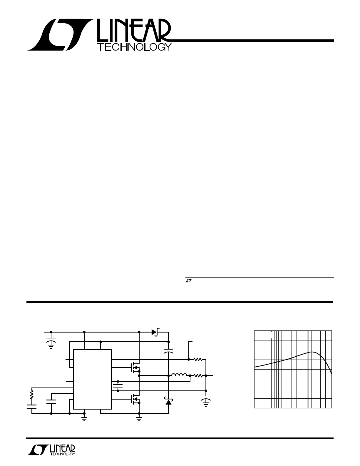
*COILTRONICS CTXO212801
V
IN
4V TO 9V
+
LOW BAT IN
0V = NORMAL
>1.5V = SHUTDOWN
RC
470Ω
CC
3300pF
U
O
A
PPLICATITYPICAL
MBR0530T1
CIN
100µF
×2
CT
180pF
VIN PWR V
LB
IN
PINV
LTC1266-3.3
SHDN
I
TH
C
T
SGND
LB
OUT
TDRIVE
SENSE
SENSE
BDRIVEBINH
PGND
IN
N-CHANNEL
Si9410
+
1000pF
–
N-CHANNEL
Si9410
Figure 1. High Efficiency Step-Down Converter
D2
LOW BAT OUT
CB
0.1µF
L*
5µH
D1
MBRS130LT3
LTC1266 • TA01
100k
R
SENSE
0.02Ω
V
OUT
3.3V
5A
+
C
OUT
330µF
× 2
LTC1266-3.3 Efficiency
1
LTC1266
LTC1266 - 3. 3/LTC1266 -5
W
O
A
LUTEXI T
S
Input Supply Voltage (Pins 2, 5)............... 20V to – 0.3V
Continuous Output Current (Pins 1, 16) .............. 50mA
Sense Voltages (Pins 8, 9)........................ 13V to – 0.3V
PINV, BINH, SHDN, LB
(Pins 3, 4, 11, 13) .................................20V to – 0.3V
LB
Output Current ........................................... 12mA
OUT
Operating Ambient Temperature Range ...... 0°C to 70°C
Extended Commercial
Temperature Range ........................... –40°C to 85°C
Junction Temperature (Note 1)............................ 125°C
Storage Temperature Range ................ –65°C to 150°C
Lead Temperature (Soldering, 10 sec)................. 300°C
LECTRICAL C CHARA TERIST
E
SYMBOL PARAMETER CONDITIONS MIN TYP MAX UNITS
V
FB
I
FB
V
OUT
∆V
I
Q1
I
Q2
V
SENSE 1
OUT
Feedback Voltage VIN = 9V, I
LTC1266ACS Topside Switch = N-Ch
LTC1266CS
Feedback Current (LTC1266 Only) ● 0.2 1 µA
Regulated Output Voltage VIN = 9V, I
LTC1266CS-3.3 Topside Switch = N-Ch, V
LTC1266CS-5
Output Ripple (Burst Mode Operation) I
Output Voltage Line Regulation I
Output Voltage Load Regulation 5mA < I
LTC1266-3.3 Burst Mode Operation Enabled, V
LTC1266-3.3 Burst Mode Operation Inhibited, V
LTC1266-5 Burst Mode Operation Enabled, V
LTC1266-5 Burst Mode Operation Inhibited, V
VIN Pin DC Supply Current (Note 2)
Normal Mode 3.5V < V
Sleep Mode 3.5V < V
Shutdown V
PWR VIN DC Supply Current (Note 2)
Normal Mode 3.5V < PWR V
Sleep Mode 3.5V < PWR V
Shutdown V
Current Sense Threshold V
(Burst Mode Operation Enabled)
LTC1266 V
LTC1266-3.3 V
LTC1266-5 V
A
IN
WUW
U
/
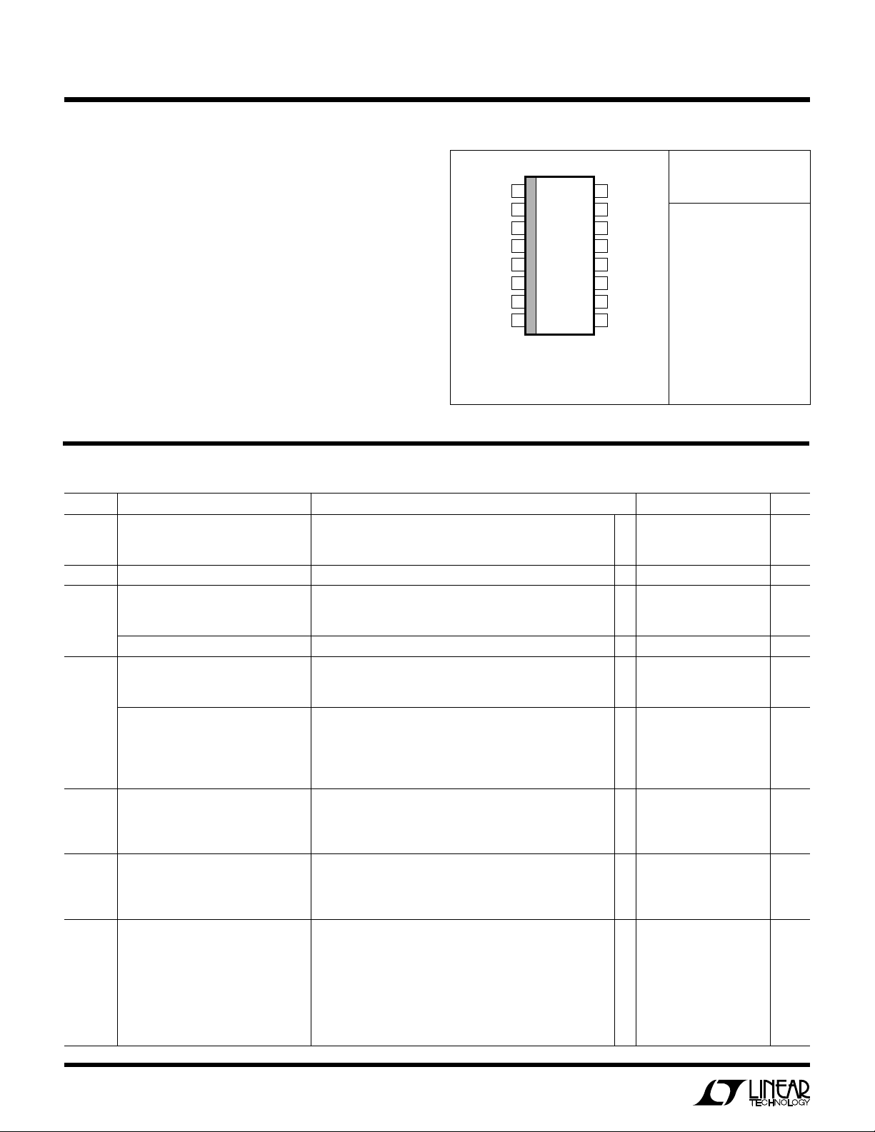
TOP VIEW
S PACKAGE
= 125°C, θ
SHDN
O
RDER I FOR ATIO
BDRIVE
16
PGND
15
LB
14
OUT
LB
13
IN
SGND
12
SHDN
11
V
(NC*)
10
FB
+
SENSE
9
= 110°C/W
JA
= V
= 0V unless otherwise noted.
BINH
● 1.275 V
● 1.210 1.25 1.290 V
● 4.90 5.05 5.20 V
LTC1266CS
LTC1266CS-3.3
LTC1266CS-5
LTC1266ACS
ARB
LOAD
LOAD
SHDN
SHDN
BINH
G
S
I
ICS
= 150mA 50 mV
= 50mA
V
PINV
V
PINV
= 2.1V, 3.5V < VIN < 18V 25 50 µA
= 2.1V, 3.5V < PWR VIN < 18V 1 5 µA
= 0V
SENSE
V
SENSE
SENSE
V
SENSE
SENSE
V
SENSE
TA = 25°C, VIN = 10V, V
= 700mA, V
LOAD
= 700mA, V
LOAD
= 0V, Topside Switch = P-Ch, VIN = 7V to 12V –40 0 40 mV
= V
, Topside Switch = N-Ch, VIN = 7V to 12V –40 0 40 mV
PWR
< 2A, R
LOAD
< 18V 2.1 3.0 mA
IN
< 18V 170 250 µA
IN
< 18V 20 40 µA
IN
< 18V 1 5 µA
IN
–
= 3.3V, VFB = V
–
= 3.3V, VFB = V
–
= V
+ 100mV (Forced) 25 mV
OUT
–
= V
– 100mV (Forced) ● 135 155 175 mV
OUT
–
= V
+ 100mV (Forced) 25 mV
OUT
–
= V
– 100mV (Forced) ● 135 155 175 mV
OUT
PACKAGE
TDRIVE
1
PWR V
Consult factory for Industrial and Military grade parts.
= V
PINV
= V
PINV
= 14V ● 3.23 3.33 3.43 V
PWR
= 0.05Ω
SENSE
/2.64 + 25mV (Forced) 25 mV
OUT
/2.64 – 25mV (Forced) ● 135 155 175 mV
OUT
2
IN
PINV
3
BINH
4
V
5
IN
C
6
T
I
7
TH
–
SENSE
8
16-LEAD PLASTIC SO
*FIXED OUTPUT VERSIONS
T
JMAX
,
PWR
,
PWR
= 0V ● 40 65 mV
BINH
= 2V ● 15 25 mV
BINH
= 0V ● 60 100 mV
BINH
= 2V ● 25 40 mV
BINH
WU
ORDER PART
NUMBER
P-P
U
2
LTC1266
LTC1266-3.3/LTC1266 -5
LECTRICAL C CHARA TERIST
E
SYMBOL PARAMETER CONDITIONS MIN TYP MAX UNITS
V
SENSE 2
V
SHDN
I
SHDN
I
PINV
V
BINH
I
BINH
I
CT
t
OFF
t
MAX
tr, t
V
CLAMP
V
LBTRIP
I
LBLEAK
I
LBSINK
I
LBIN
Current Sense Threshold V
(Burst Mode Operation Disabled)
LTC1266 V
LTC1266-3.3 V
LTC1266-5 V
Shutdown Pin Threshold 0.6 0.8 2 V
Shutdown Pin Input Current 0V < V
Phase Invert Pin Input Current 0V < V
Burst Mode Operation 0.8 1.2 2 V
Inhibit Pin Threshold
Burst Mode Operation 0V < V
Inhibit Pin Input Current
CT Pin Discharge Current V
Off-Time (Note 3) CT = 390pF, I
Max On-Time V
Driver Output Transition Times CL = 3000pF (Pins 1, 16), VIN = 6V 100 200 ns
f
Output Voltage Clamp in V
Burst Mode Operation Inhibit
LTC1266 Measured at V
LTC1266-3.3 Measured at V
LTC1266-5 Measured at V
Low-Battery Trip Point VIN = 5V 1.14 1.25 1.35 V
Max Leakage Current into Pin 14 V
Max Sink Current into Pin 14 V
Max Leakage Current into Pin 13 V
ICS
= 2.1V
BINH
SENSE
V
SENSE
SENSE
V
SENSE
SENSE
V
SENSE
SENSE
V
= 0V 2 10 µA
OUT
= 0V, VIN = 18V 60 µs
OUT
= 2.1V
BINH
= 12V 1.17 1.30 1.42 V
V
IN
LBOUT
LBOUT
= 18V 0.2 1 µA
LBIN
TA = 25°C, VIN = 10V, V
–
= 3.3V, VFB = V
–
= 3.3V, VFB = V
–
= V
+ 100mV (Forced) –20 mV
OUT
–
= V
– 100mV (Forced) ● 135 155 175 mV
OUT
–
= V
+ 100mV (Forced) –20 mV
OUT
–
= V
– 100mV (Forced) ● 135 155 175 mV
OUT
< 8V, VIN = 16V 1.2 5 µA
SHDN
< 18V, VIN = 18V 0.2 1 µA
PINV
< 18V, VIN = 18V 0.2 1 µA
BINH
+
= V
– 100mV, V
OUT
= 700mA 4 5 6 µs
LOAD
FB
SENSE
SENSE
= 18V, V
= 1V, V
= 2V 25 200 nA
LBIN
= 0V, 2.5V < VIN < 18V 1 8 mA
LBIN
/2.64 + 25mV (Forced) – 20 mV
OUT
/2.64 – 25mV (Forced) ● 135 155 175 mV
OUT
–
= V
SENSE
–
–
OUT
= V
SHDN
= 0V unless otherwise noted.
BINH
– 300mV 50 70 90 µA
1.30 V
3.43
5.20 V
V
–40°C < TA < 85°C (Note 4), VIN = 10V, unless otherwise noted.
SYMBOL PARAMETER CONDITIONS MIN TYP MAX UNITS
V
FB
V
OUT
Feedback Voltage (LTC1266 only) VIN = 9V, I
Regulated Output Voltage VIN = 9V, I
= 700mA 1.21 1.25 1.29 V
LOAD
= 700mA
LOAD
LTC1266-3.3 3.23 3.33 3.43 V
LTC1266-5 4.90 5.05 5.20 V
I
Q1
I
Q2
VIN Pin DC Supply Current (Note 2)
Normal Mode 3.5V < V
Sleep Mode 3.5V < V
Shutdown V
IN
IN
SHUTDOWN
PWR VIN DC Supply Current (Note 2)
Normal Mode 3.5V < PWR V
Sleep Mode 3.5V < PWR V
Shutdown V
SHUTDOWN
< 18V 2.1 3.3 mA
< 18V 170 260 µA
= 2.1V, 3.5V < VIN < 18V 25 60 µA
< 18V 20 50 µA
IN
< 18V 1 7 µA
IN
= 2.1V, 3.5V < PWR VIN < 18V 1 7 µA
3
LTC1266
LTC1266 - 3. 3/LTC1266 -5
LECTRICAL C CHARA TERIST
E
SYMBOL PARAMETER CONDITIONS MIN TYP MAX UNITS
V
SENSE1
Sense 2 Current Sense Threshold V
V
SHDN
t
OFF
Current Sense Threshold V
(Burst Mode Operation Enabled)
LTC1266 V
LTC1266-3.3, LTC1266-5 V
(Burst Mode Operation Disabled)
LTC1266 V
LTC1266-3.3, LTC1266-5 V
Shutdown Pin Threshold 0.55 0.8 2 V
Off-Time (Note 3) CT = 390pF, I
BINH
SENSE
V
SENSE
SENSE
V
SENSE
BINH
SENSE
V
SENSE
SENSE
V
SENSE
= 0V
= 2.1V
ICS
–
= 3.3V, VFB = V
–
= 3.3V, VFB = V
–
= V
+ 100mV (Forced) 25 mV
OUT
–
= V
– 100mV (Forced) 135 155 180 mV
OUT
–
3.3V, VFB = V
–
3.3V, VFB = V
–
= V
+ 100mV (Forced) –20 mV
OUT
–
= V
– 100mV (Forced) 130 155 185 mV
OUT
= 700mA 3.8 5 6.5 µs
LOAD
/2.64 + 25mV (Forced) 25 mV
OUT
/2.64 – 25mV (Forced) 135 155 180 mV
OUT
/2.64 + 25mV (Forced) –20 mV
OUT
/2.64 – 25mV (Forced) 130 155 185 mV
OUT
The ● denotes specifications which apply over the full operating
temperature range.
Note 1: T
dissipation P
is calculated from the ambient temperature TA and power
J
according to the following formula:
D
TJ = TA + (PD × 110°C/W)
Note 2: Dynamic supply current is higher due to the gate charge being
delivered at the switching frequency. See Applications Information.
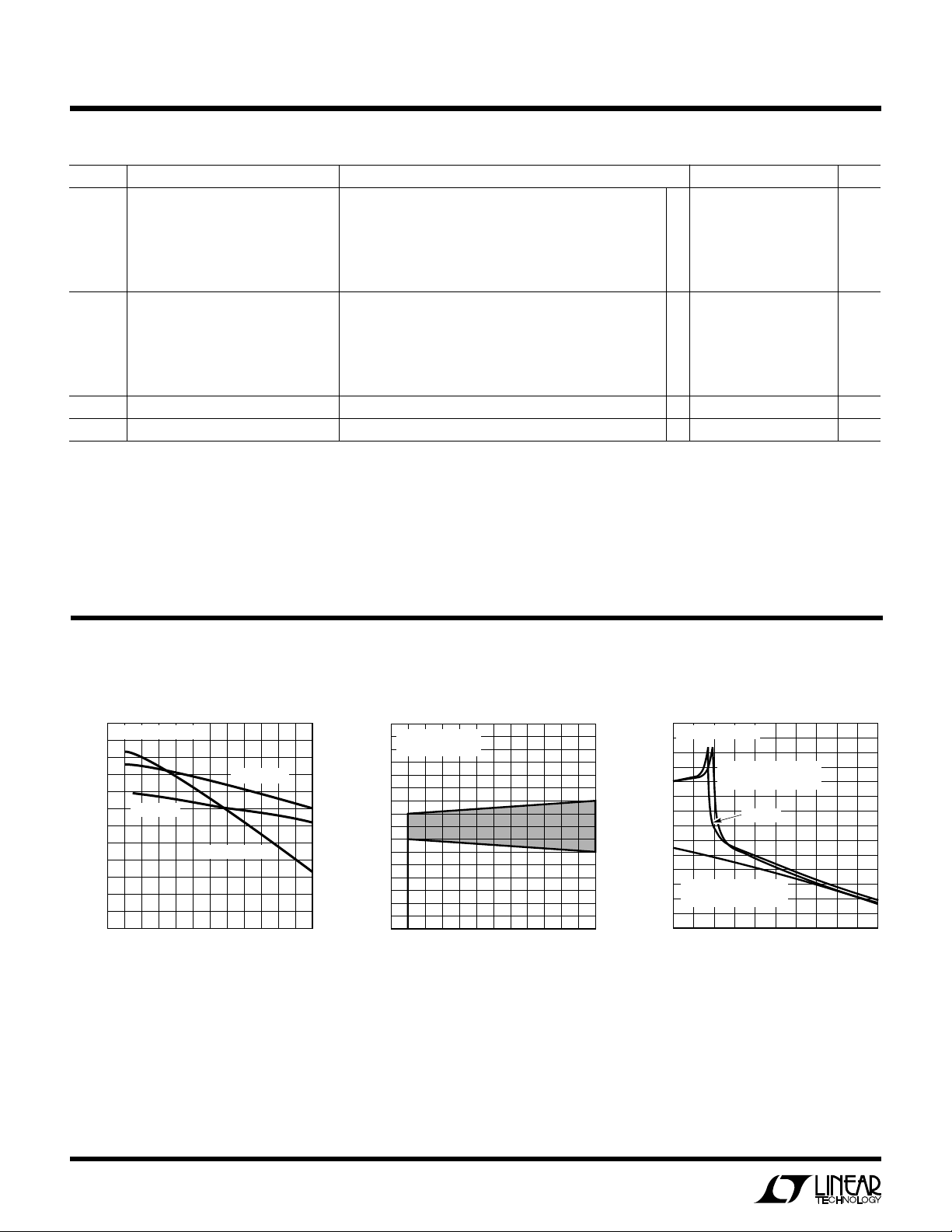
UW
LPER
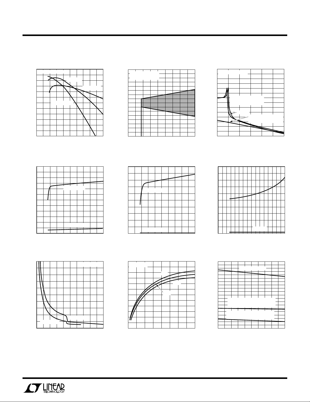
Efficiency vs Input Voltage
100
FIGURE 1 CIRCUIT
95
90
I
= 5A
LOAD
85
EFFICIENCY (%)
80
75
70
3
567
4
INPUT VOLTAGE (V)
F
I
LOAD
R
O
I
LOAD
= 100mA
ATYPICA
= 2.5A
89
LTC1266 • TPC01
CCHARA TERIST
E
C
Line Regulation Load Regulation
40
FIGURE 1 CIRCUIT
= 1A
I
LOAD
30
20
10
(mV)
0
OUT
∆V
–10
–20
–30
–40
45678
3
Note 3: In applications where R
is placed at ground potential, the off-
SENSE
time increases approximately 40%.
Note 4: The LTC1266, LTC1266-3.3, and LTC1266-5 are not tested and
not quality assurance sampled at –40°C and 85°C. These specifications
are guaranteed by design and/or correlation.
Note 5: Unless otherwise noted the specifications for the LTC1266A are
the same as those for the LTC1266.
ICS
20
FIGURE 1 CIRCUIT
INPUT VOLTAGE (V)
LTC1266 • TPC02
10
0
–10
(mV)
OUT
–20
∆V
–30
–40
–50
9
0
VIN = 9V (Burst Mode
OPERATION ENABLED)
VIN = 5V
VIN = 5V (Burst Mode
OPERATION INHIBITED)
1
2
LOAD CURRENT (A)
3
4
LTC1266 • TPC03
5
4
LPER
LOAD CURRENT (A)
0
–40
∆V
OUT
(mV)
–30
–20
–10
30
10
0.5
1.0
20
0
1.5
2.0 2.5
3.0
LTC1266 • TPC06
FIGURE 11 CIRCUIT
V
IN
= 12V (Burst Mode
OPERATION ENABLED)
VIN = 5V
VIN = 5V (Burst Mode
OPERATION INHIBITED)
INPUT VOLTAGE (V)
0
SUPPLY CURRENT (µA)
30
40
50
LTC1266 • TPC09
20
10
0
5
10
15
20
V
IN
PWR V
IN
TEMPERATURE (°C)
0
SENSE VOLTAGE (mV)
100
150
200
80
LTC1266 • TPC12
50
0
–50
20
40
60
100
MAX THRESHOLD
MIN THRESHOLD (Burst Mode
OPERATION INHIBIT)
MIN THRESHOLD (Burst Mode
OPERATION ENABLED)
F
O
R
ATYPICA
UW
CCHARA TERIST
E
C
LTC1266
LTC1266-3.3/LTC1266 -5
ICS
100
95
90
85
EFFICIENCY (%)
80
75
70
3.0
2.5
2.0
1.5
1.0
SUPPLY CURRENT (mA)
0.5
100
80
60
40
OFF-TIME (µs)
20
Efficiency vs Input Voltage
FIGURE 11 CIRCUIT
I
= 1A
LOAD
I
= 100mA
LOAD
4
0
INPUT VOLTAGE (V)
12
8
VIN DC Supply Current
ACTIVE MODE
SLEEP MODE
0
4
0
INPUT VOLTAGE (V)
12
8
Off-Time vs Output Voltage
V
LTC1266-3.3
0
01
OUTPUT VOLTAGE (V)
LTC1266-5
2
34
I
LOAD
SENSE
LTC1266 • TPC10
= 2.5A
16
LTC1266 • TPC04
16
LTC1266 • TPC07
–
= V
OUT
Line Regulation
40
FIGURE 11 CIRCUIT
= 1A
I
LOAD
30
20
10
(mV)
0
OUT
∆V
–10
–20
–30
20
–40
0
812
4
INPUT VOLTAGE (V)
16
LTC1266 • TPC05
Power VIN DC Supply Current
25
20
V
OUT
ACTIVE MODE
SLEEP MODE
4
INPUT VOLTAGE (V)
OUT
= 3.3V
2
4
(VIN – V
8
) Voltage
0°C
25°C
6
) VOLTAGE (V)
OUT
12
16
20
LTC1266 • TPC08
70°C
12108
14
LTC1266 • TPC11
16
15
10
SUPPLY CURRENT (µA)
5
20
0
0
Operating Frequency
vs (VIN – V
3.0
2.5
2.0
1.5
1.0
NORMALIZED FREQUENCY
0.5
5
0
0
Load Regulation
Supply Current in Shutdown
Current Sense Threshold Voltage
5

LTC1266
LTC1266 - 3. 3/LTC1266 -5
U
UU
PI FU CTIO S
TDrive (Pin 1): High Current Drive for Topside MOSFET.
This MOSFET can be either P-channel or N-channel, user
selectable by Pin 3. Voltage swing at this pin is from PWR
VIN to ground.
PWR VIN (Pin 2): Power Suppy for Drive Signals. Must be
closely decoupled to power ground (Pin 15).
PINV (Pin 3): Phase Invert. Sets the phase of the topside
driver to drive either a P-channel or an N-channel MOSFET
as follows:
P-channel: Pin 3 = 0V
N-channel: Pin 3 = PWR V
BINH (Pin 4): Burst Mode Operation Inhibit. A CMOS logic
high on this pin will disable the Burst Mode operation
feature forcing continuous operation down to zero load.
VIN (Pin 5): Main Supply Pin.
CT (Pin 6): External Capacitor. CT from Pin 4 to ground sets
the operating frequency. The actual frequency is also
dependent on the input voltage.
ITH (Pin 7): Gain Amplifier Decoupling Point. The current
comparator threshold increases with the Pin 7 voltage.
Sense– (Pin 8): Connects to internal resistive divider
which sets the output voltage in LTC1266-3.3 and
LTC1266-5 versions. Pin 8 is also the (–) input for the
current comparator.
IN
Sense+ (Pin 9): The (+) Input to the Current Comparator.
A built-in offset between Pins 8 and 9 in conjunction with
R
VFB (Pin 10): For the LTC1266 adjustable version, Pin 10
serves as the feedback pin from an external resistive
divider used to set the output voltage. On LTC1266-3.3
and LTC1266-5 versions this pin is not used.
SHDN (Pin 11): When grounded, the LTC1266 series
operates normally. Pulling Pin 11 high holds both MOSFETs
off and puts the LTC1266 in micropower shutdown mode.
Requires CMOS logic signal with tr, tf < 1µ s. Should not be
left floating.
SGND (Pin 12): Small-Signal Ground. Must be routed
separately from other grounds to the (–) terminal of C
LBIN (Pin 13): Input to the Low-Battery Comparator. This
input is compared to an internal 1.25V reference.
LB
Comparator. This pin will sink current when Pin 13 is
below 1.25V.
PGND (Pin 15): Driver Power Ground. Connects to source
of N-channel MOSFET and the (–) terminal of CIN.
BDrive (Pin 16): High Current Drive for Bottom N-Channel MOSFET. Voltage swing at Pin 16 is from ground to
PWR VIN.
sets the current trip threshold.
SENSE
(Pin 14): Open Drain Output of the Low-Battery
OUT
OUT
.
6
 Loading...