

Linear Technology LTC1265, LTC1265IS, LTC1265CS, LTC1265-5, LTC1265CS-5 Datasheet
...
FEATURES
LTC1265/LTC1265-3.3/LTC1265-5
1.2A, High Efficiency
Step-Down DC/DC Converter
U
DESCRIPTIO
■
High Efficiency: Up to 95%
■
Current Mode Operation for Excellent Line and Load
Transient Response
■
Internal 0.3Ω Power Switch (VIN = 10V)
■
Short-Circuit Protection
■
Low Dropout Operation: 100% Duty Cycle
■
Low-Battery Detector
■
Low 160µA Standby Current at Light Loads
■
Active-High Micropower Shutdown: IQ < 15µA
■
Peak Inductor Current Independent of Inductor Value
■
Available in 14-pin SO Package
U
APPLICATIO S
■
5V to 3.3V Conversion
■
Distributed Power Systems
■
Step-Down Converters
■
Inverting Converters
■
Memory Backup Supply
■
Portable Instruments
■
Battery-Powered Equipment
■
Cellular Telephones
The LTC®1265 is a monolithic step-down current mode
DC/DC converter featuring Burst Mode TM operation at low
output current. The LTC1265 incorporates a 0.3Ω switch
(VIN =10V) allowing up to 1.2A of output current.
Under no load condition, the converter draws only 160µA.
In shutdown it typically draws a mere 5µA making this
converter ideal for current sensitive applications. In dropout the internal P-channel MOSFET switch is turned on
continuously maximizing the life of the battery source. The
LTC1265 incorporates automatic power saving Burst Mode
operation to reduce gate charge losses when the load
currents drop below the level required for continuous
operation.
The inductor current is user-programmable via an external
current sense resistor. Operation up to 700kHz permits
the use of small surface mount inductors and capacitors.
, LTC and LT are registered trademarks of Linear Technology Corporation.
Burst Mode is a trademark of Linear Technology Corporation.
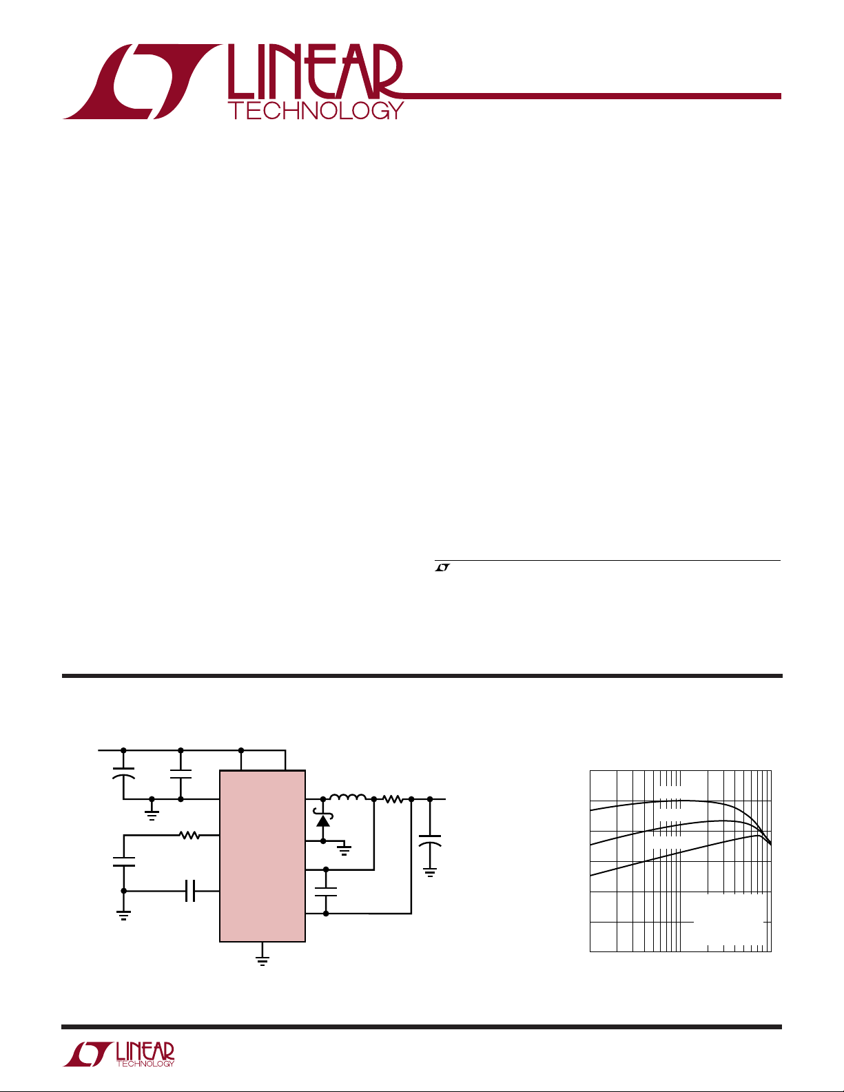
TYPICAL APPLICATIO
V
IN
5.4V TO
12V
†††
+
C
IN
68µF
20V
3900pF
1k
130pF
0.1µF
PWR V
SHDN
I
TH
C
T
IN
LTC1265-5
SGND
Figure 1. High Efficiency Step-Down Converter
U
V
PGND
SENSE
SENSE
IN
SW
LTC1265-5 Efficiency
L1*
33µH
†
D1
+
1000pF
–
COILTRONICS CTX33-4
*
IRC LRC2010-01-R100-J
**
†
MBRS130LT3
††
AVX TPSE227K010
†††
AVX TPSE686K020
R
SENSE
0.1Ω
**
V
OUT
5V
1A
††
C
+
OUT
220µF
10V
LTC1265-FO1
100
95
90
85
EFFICIENCY (%)
80
75
70
0.01
VIN = 6V
VIN = 9V
VIN = 12V
L = 33µH
V
OUT
R
SENSE
C
T
0.10 1.00
LOAD CURRENT (A)
= 5V
= 0.1Ω
= 130pF
LTC1265 TA01
1
LTC1265/LTC1265-3.3/LTC1265-5
WW
W
ABSOLUTE MAXIMUM RATINGS
U
U
W
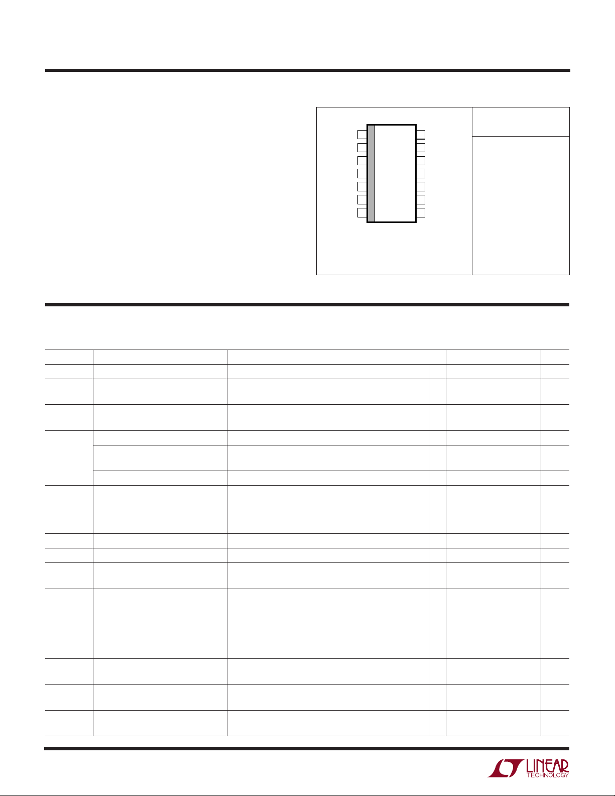
PACKAGE/ORDER INFORMATION
U
(Voltages Refer to GND Pin) (Note 1)
Input Supply Voltage (Pins 1, 2, 13)..........–0.3V to 13V
DC Switch Current (Pin 14) .................................... 1.2A
Peak Switch Current (Pin 14) ................................. 1.6A
Switch Voltage (Pin 14) ..................................V
– 13.0
IN
Operating Temperature Range
LTC1265C ............................................... 0° to 70°C
LTC1265I ........................................ – 40°C to 85°C
Junction Temperature (Note 2)............................. 125°C
Storage Temperature Range ....................– 65° to 150°C
Lead Temperature (Soldering, 10 sec)..................300°C
PWR V
LB
SENSE
OUT
LB
TOP VIEW
1
IN
2
V
IN
3
4
IN
5
C
T
6
I
TH
–
7
S PACKAGE
14-LEAD PLASTIC SO
*ADJUSTABLE OUTPUT VERSION
T
= 125°C, θJA = 110°C/W
JMAX
14
SW
13
PWR V
12
PGND
11
SGND
10
SHDN
9
N/C (V
8
SENSE
IN
*)
FB
+
Consult factory for Military grade parts.
ELECTRICAL CHARACTERISTICS
temperature range, otherwise specifications are at TA = 25°C. VIN = 10V, V
The ● denotes the specifications which apply over the full operating
= 0V, unless otherwise specified.
SHDN
SYMBOL PARAMETER CONDITIONS MIN TYP MAX UNITS
I
FB
V
FB
V
OUT
∆V
OUT
I
Q
V
LBTRIP
I
LBIN
I
LBOUT
V8 – V
R
ON
7
Feedback Current into Pin 9 LTC1265 0.2 1 µA
Feedback Voltage LTC1265C ● 1.22 1.25 1.28 V
= 9V, LTC1265I ● 1.20 1.25 1.30 V
V
IN
Regulator Output Voltage LTC1265-3.3: I
LTC1265-5: I
Output Voltage Line Regulation VIN = 6.5V to 10V, I
Output Voltage Load Regulation LTC1265-3.3: 10mA < I
LTC1265-5: 10mA < I
Burst Mode Operation Output Ripple I
= 0mA 50 mV
LOAD
= 800mA ● 3.22 3.3 3.40 V
LOAD
= 800mA ● 4.9 5 5.2 V
LOAD
= 800mA –40 0 40 mV
LOAD
< 800mA 40 65 mV
LOAD
< 800mA 60 100 mV
LOAD
Input DC Supply Current (Note 3) Active Mode: 3.5V < VIN < 10V 1.8 2.4 mA
Sleep Mode: 3.5V < V
Sleep Mode: 5V < V
Shutdown: V
SHDN
< 10V 160 230 µA
IN
< 10V (LTC1265-5) 160 230 µA
IN
= VIN, 3.5V < VIN < 10V 5 15 µA
Low-Battery Trip Point 1.15 1.25 1.35 V
Current into Pin 4 0.5 µA
Current Sunk by Pin 3 V
Current Sense Threshold Voltage LTC1265: V
= 0.4V, V
LBOUT
= 5V, V
V
LBOUT
V
SENSE
SENSE
LTC1265-3.3: V
V
LTC1265-5: V
V
SENSE
SENSE
= 0V 0.5 1.0 1.5 mA
LBIN
= 10V 1.0 µA
LBIN
–
= 5V, V9 = V
–
= 5V, V9 = V
–
= V
SENSE
–
= V
SENSE
–
= V
–
= V
OUT
OUT
/4 + 25mV (Forced) 25 mV
OUT
/4 – 25mV (Forced) 130 150 180 mV
OUT
+ 100mV (Forced) 25 mV
OUT
– 100mV (Forced) 130 150 180 mV
OUT
+ 100mV (Forced) 25 mV
– 100mV (Forced) 130 150 180 mV
ON Resistance of Switch LTC1265C ● 0.3 0.60 Ω
LTC1265I 0.3 0.70 Ω
I
t
5
OFF
CT Pin Discharge Current V
in Regulation, V
OUT
= 0V 2 10 µA
V
OUT
Switch Off Time (Note 4) CT = 390pF, I
C
= 390pF, I
T
= 800mA (LTC1265C) ● 456 µs
LOAD
= 800mA (LTC1265I) ● 3.5 5 7 µs
LOAD
SENSE
–
= V
OUT
40 60 100 µA
ORDER
PART NUMBER
LTC1265CS
LTC1265CS-5
LTC1265CS-3.3
LTC1265IS
P-P
2
LTC1265/LTC1265-3.3/LTC1265-5
INPUT VOLTAGE (V)
4
80
EFFICIENCY (%)
82
86
88
90
100
94
6
8
913
LTC1265 G03
84
96
98
92
57
10
11
12
I
LOAD
= 250mA
I
LOAD
= 800mA
LTC1265-3.3
R
SENSE
= 0.1Ω
C
T
= 130pF
COIL = CTX33-4
ELECTRICAL CHARACTERISTICS
temperature range, otherwise specifications are at TA = 25°C. VIN = 10V, V
The ● denotes the specifications which apply over the full operating
= 0V, unless otherwise specified.
SHDN
SYMBOL PARAMETER CONDITIONS MIN TYP MAX UNITS
V
IH
V
IL
I
10
Note 1: Absolute Maximum Ratings are those values beyond which the life
of the device may be impaired.
Note 2: T
dissipation P
Shutdown Pin High Min Voltage at Pin 10 for Device to be in Shutdown 1.2 V
Shutdown Pin Low Max Voltage at Pin 10 for Device to be Active 0.6 V
Shutdown Pin Input Current V
= 8V 0.5 µA
SHDN
Note 3: Dynamic supply current is higher due to the gate charge being
delivered at the switching frequency.
is calculated from the ambient temperature TA and power
J
according to the following formulas:
D
Note 4: In applications where R
off time increases by approximately 40%.
is placed at ground potential, the
SENSE
LTC1265CS, LTC1265CS-3.3, LTC1265CS-5:
TJ = TA + (PD • 110°C/W)
W
U
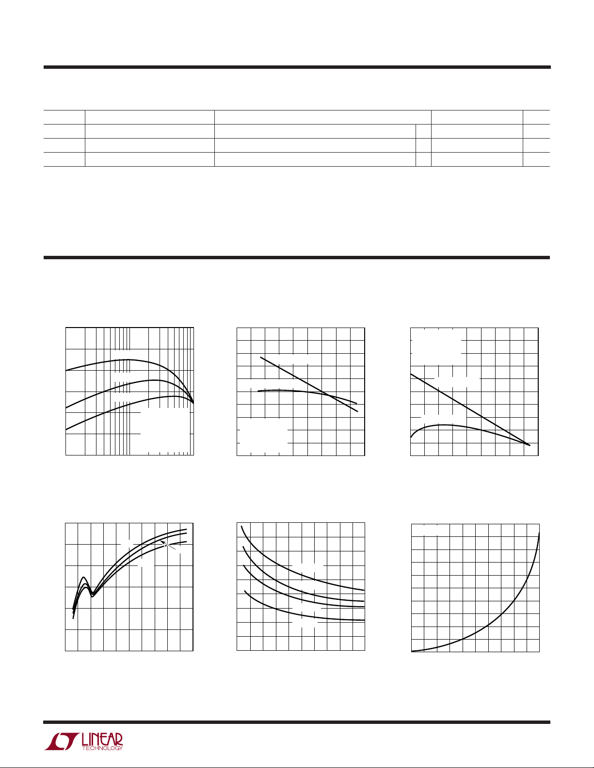
TYPICAL PERFORMANCE CHARACTERISTICS
Efficiency vs Load Current
100
95
90
85
EFFICIENCY (%)
80
75
70
0.01
VIN = 5V
VIN = 9V
VIN = 12V
0.10 1.00
LOAD CURRENT (A)
LTC1265-3.3
= 3.3V
V
OUT
= 0.1Ω
R
SENSE
= 130pF
C
T
COIL = CTX33-4
1265 G01
Efficiency vs Input Voltage
(V
= 5V)
OUT
100
98
96
94
92
90
88
EFFICIENCY (%)
86
LTC1265-5
84
R
SENSE
C
T
82
COIL = CTX33-4
80
4
I
= 250mA
LOAD
I
= 800mA
LOAD
= 0.1Ω
= 130pF
57
6
8
INPUT VOLTAGE (V)
11
913
12
10
1265 G02
Efficiency vs Input Voltage
(V
= 3.3V)
OUT
Operating Frequency
vs (V
– V
IN
1.2
1.0
0.8
0.6
0.4
NORMALIZED FREQUENCY
0.2
0
OUT
21468
(V
IN – VOUT
)
0°C
70°C
) VOLTAGE (V)
25°C
1265 G04
1003579
Switch Resistance
0.9
0.8
0.7
0.6
(Ω)
0.5
(ON)
0.4
RDS
0.3
0.2
0.1
0
3
48
59
= 125°C
T
J
T
= 70°C
J
T
= 25°C
J
T
= 0°C
J
6
7
INPUT VOLTAGE (V)
Switch Leakage Current
300
VIN = 12V
270
240
210
180
150
120
90
LEAKAGE CURRENT (nA)
60
30
12
10
13
11
1265 G05
0
20
0
TEMPERATURE (°C)
60
80
40
100
1265 G06
3
LTC1265/LTC1265-3.3/LTC1265-5
W
U
TYPICAL PERFORMANCE CHARACTERISTICS
DC Supply Current
2.1
DOES NOT INCLUDE
GATE CHARGE
1.8
1.5
1.2
0.9
0.6
SUPPLY CURRENT (mA)
0.3
0
0
4
2
INPUT VOLTAGE (V)
ACTIVE MODE
SLEEP MODE
10
814
6
12
1265 G07
Supply Current in Shutdown Gate Charge Losses
8
SHUTDOWN = 3V
T
= 25C
A
7
6
5
4
3
SUPPLY CURRENT (µA)
2
1
0
4
5
3
6
7
INPUT VOLTAGE (V)
UUU
PIN FUNCTIONS
PWR V
its Driver. Must decouple this pin properly to ground. Must
always tie Pins 1 and 13 together.
V
IN
LTC1265.
LB
Comparator. This pin will sink current when Pin 4 (LBIN)
goes below 1.25V. During shutdown, this pin is high
impedance.
LB
The (+) input is connected to a reference voltage of 1.25V.
CT (Pin 5): External capacitor CT from Pin 5 to ground sets
the switch off time. The operating frequency is dependent
on the input voltage and CT.
I
TH
current comparator threshold is proportional to Pin 6
voltage.
SENSE– (Pin 7): Connect to the (–) input of the current
comparator. For LTC1265-3.3 and LTC1265-5, it also
connects to an internal resistive divider which sets the
output voltage.
(Pins 1, 13): Supply for the Power MOSFET and
IN
(Pin 2): Main Supply for All the Control Circuitry in the
(Pin 3): Open-Drain Output of the Low-Battery
OUT
(Pin 4): The (–) Input of the Low-Battery Comparator.
IN
(Pin 6): Feedback Amplifier Decoupling Point. The
5.5
5.0
4.5
4.0
3.5
3.0
2.5
2.0
1.5
SWITCHING CURRENT (mA)
1.0
0.5
0
200 400
8
9
11
10
12
13
1265 G08
0
FREQUENCY (kHz)
600
VIN = 12V
VIN = 9V
VIN = 6V
800 1000
1265 G09
SENSE+ (Pin 8): The (+) Pin to the Current Comparator. A
built-in offset between Pins 7 and 8 in conjunction with
R
N/C,V
sets the current trip threshold.
SENSE
(Pin 9): For the LTC1265 adjustable version, this
FB
pin serves as the feedback pin from an external resistive
divider used to set the output voltage. On the LTC1265-3.3
and LTC1265-5 versions, this pin is not used.
SHDN (Pin 10): Pulling this pin HIGH keeps the internal
switch off and puts the LTC1265 in micropower shutdown. Do not float this pin.
SGND (Pin 11): Small-Signal Ground. Must be routed
separately from other grounds to the (–) terminal of C
OUT
.
PGND (Pin 12): Switch Driver Ground. Connects to the
(–) terminal of CIN. Anode of the Schottky diode must be
connected close to this pin.
SW (Pin 14): Drain of the P-Channel MOSFET Switch.
Cathode of the Schottky diode must be connected close to
this pin.
4
LTC1265/LTC1265-3.3/LTC1265-5
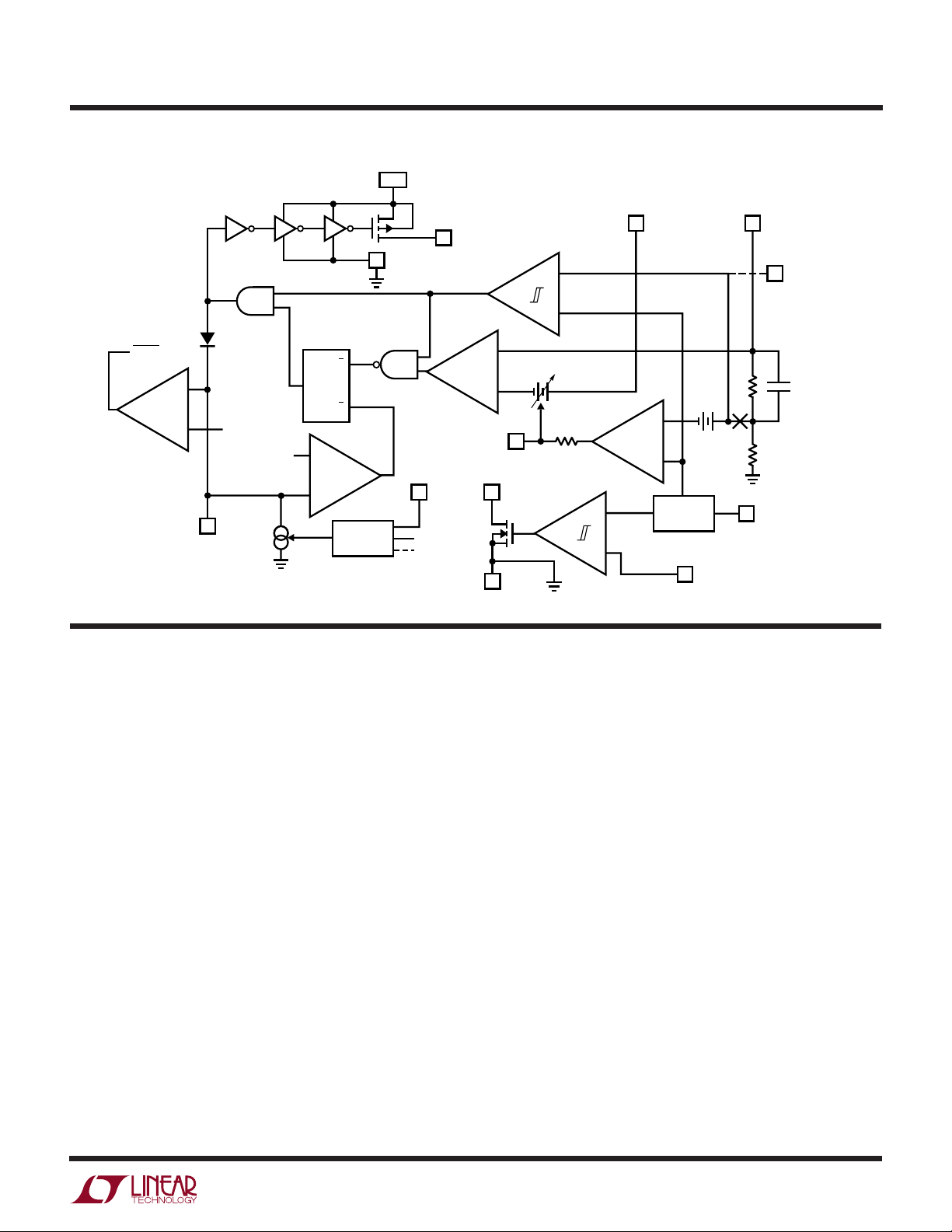
UU
W
FUNCTIONAL DIAGRA
SLEEP
+
S
–
V
TH2
5
C
T
Q
V
–
TH1
+
(Pin 9 connection shown for LTC1265-3.3 and LTC1265-5; change create LTC1265)
PWR V
1, 13
PGND
12
IN
+
SENSE
SW
14
–
V
+
SENSE
78
–
9
V
FB
ADJUSTABLE
VERSION
–
R
S
T
OFF-TIME
CONTROL
V
2 3
IN
–
SENSE
V
FB
C
+
I
TH
LB
11
SGND
25mV TO 150mV
13k
6
0UT
A3
V
OS
–
G
+
+
–
REFERENCE
4
10
SHDN
LB
IN
5pF
100k
1265 FD
U
OPERATION
The LTC1265 uses a constant off-time architecture to
switch its internal P-channel power MOSFET. The off time
is set by an external timing capacitor at CT (Pin 5). The
operating frequency is then determined by the off time and
the difference between VIN and V
The output voltage is set by an internal resistive divider
(LTC1265-3.3 and LTC1265-5) connected to SENSE
(Pin 7) or an external divider returned to VFB (Pin 9 for
LTC1265). A voltage comparator V, and a gain block G,
compare the divided output voltage with a reference
voltage of 1.25V.
To optimize efficiency, the LTC1265 automatically switches
between continuous and Burst Mode operation. The voltage comparator is the primary control element when the
device is in Burst Mode operation, while the gain block
controls the output voltage in continuous mode.
When the load is heavy, the LTC1265 is in continuous
operation. During the switch ON time, current comparator
C monitors the voltage between Pins 7 and 8 connected
across an external shunt in series with the inductor. When
(Refer to Functional Diagram)
.
OUT
–
the voltage across the shunt reaches the comparator’s
threshold value, its output signal will change state, setting
the flip flop and turning the internal P-channel MOSFET off.
The timing capacitor connected to Pin 5 is now allowed to
discharge at a rate determined by the off-time controller.
When the voltage on the timing capacitor has discharged
past V
, comparator T trips, sets the flip flop and causes
TH1
the switch to turn on. Also, the timing capacitor is recharged. The inductor current will again ramp up until the
current comparator C trips. The cycle then repeats.
When the load current increases, the output voltage decreases slightly. This causes the output of the gain stage
(Pin 6) to increase the current comparator threshold, thus
tracking the load current.
When the load is relatively light, the LTC1265 automatically goes into Burst Mode operation. The current loop is
interrupted when the output voltage exceeds the desired
regulated value. The hysteretic voltage comparator V trips
when V
is above the desired output voltage, shutting
OUT
off the switch and causing the capacitor to discharge. This
5
 Loading...