

Linear Technology LTC1261L Datasheet
FEATURES
■
Regulated Negative Voltage from a
Single Positive Supply
■
REG Pin Indicates Output is in Regulation
■
Adjustable or Fixed Output Voltages
■
Output Regulation: ±3.5%
■
Supply Current: 650µA Typ
■
Shutdown Mode Drops Supply Current to 5µA
■
Up to 20mA Output Current
■
Requires Only Three or Four External Capacitors
■
Available in MS8 and SO-8 Packages
U
APPLICATIO S
■
GaAs FET Bias Generators
■
Negative Supply Generators
■
Battery-Powered Systems
■
Single Supply Applications
LTC1261L
Switched Capacitor
Regulated Voltage Inverter
U
DESCRIPTIO
The LTC®1261L is a switched-capacitor voltage inverter
designed to provide a regulated negative voltage from a
single positive supply. The LTC1261L operates from a
single 2.7V to 5.25V supply and provides an adjustable
output voltage from –1.23V to –5V. The LTC1261L-4/
LTC1261L-4.5 needs a single 4.5V to 5.25V supply and
provides a fixed output voltage of –4V to – 4.5V respectively. Three external capacitors are required: a 0.1µF
flying capacitor and an input and output bypass capacitors. An optional compensation capacitor at ADJ (COMP)
can be used to reduce the output voltage ripple.
Each version of the LTC1261L will supply up to 20mA
output current with guaranteed output regulation of ±3.5%.
The LTC1261L includes an open-drain REG output that
pulls low when the output is within 5% of the set value.
Quiescent current is typically 650µA when operating and
5µA in shutdown.
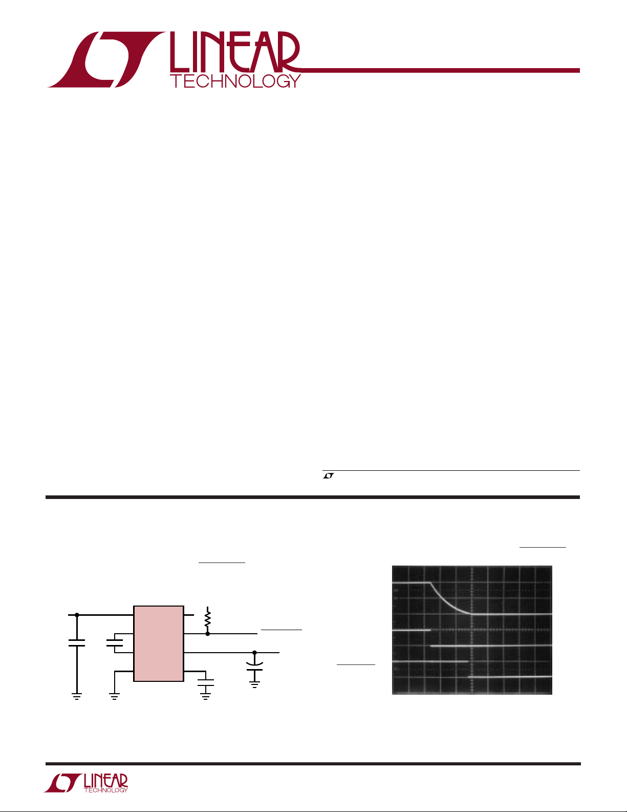
TYPICAL APPLICATION
–4V Generator with Power Valid
5V
C1
1µF
0.1µF
1
V
CC
2
+
C2
C1
3
C1
4
GND
LTC1261L-4
–
SHDN
REG
OUT
COMP
8
7
6
5
The LTC1261L is available in 8-pin MSOP and SO packages.
, LTC and LT are registered trademarks of Linear Technology Corporation.
U
Waveforms for –4V Generator with Power Valid
0V
5V
10k
POWER VALID
V
= –4V
OUT
AT 10mA
C4
3.3µF
C3*
100pF
+
*OPTIONAL
1261L TA01
OUT
SHDN
POWER VALID
–4V
5V
0V
5V
0V
0.1ms/DIV
1261L TAO2
1
LTC1261L
A
W
O
LUTEXI TIS
S
A
WUW
U
ARB
G
(Note 1)
Supply Voltage (Note 2) ........................................ 5.5V
Output Voltage (Note 3)........................... 0.3V to –5.3V
Total Voltage, VCC to V
(Note 2) ..................... 10.8V
OUT
SHDN Pin .................................. –0.3V to (VCC + 0.3V)
REG Pin ..................................................... –0.3V to 6V
ADJ Pin........................... (V
– 0.3V) to (VCC + 0.3V)
OUT
WU
/
PACKAGE
V
1
CC
+
2
C1
–
3
C1
4
GND
8-LEAD PLASTIC MSOP
T
JMAX
O
TOP VIEW
MS8 PACKAGE
= 150°C, θ
JA
RDER I FOR ATIO
ORDER PART
NUMBER
8
SHDN
7
REG
6
OUT
5
ADJ (COMP)
= 200°C/W
LTC1261LCMS8
LTC1261LCMS8-4
LTC1261LCMS8-4.5
MS8 PART MARKING
LTFM
LTFN
LTFP
Output Short-Circuit Duration......................... Indefinite
Commercial Temperature Range ................ 0°C to 70°C
Extended Commercial Operating
Temperature Range (Note 4) ................. – 40°C to 85°C
Storage Temperature Range ................ –65°C to 150°C
Lead Temperature (Soldering, 10 sec)................. 300°C
U
ORDER PART
NUMBER
LTC1261LCS8
LTC1261LCS8-4
LTC1261LCS8-4.5
S8 PART MARKING
1261L
1261L4
261L45
V
1
CC
+
C1
2
–
C1
3
GND
4
8-LEAD PLASTIC SO
T
= 150°C, θ
JMAX
TOP VIEW
S8 PACKAGE
JA
8
7
6
5
= 135°C/W
SHDN
REG
OUT
ADJ (COMP)
Consult factory for Industrial or Military grade parts or additional fixed voltage parts.
LECTRICAL C CHARA TERIST
E
temperature range, otherwise specifications are at TA = 25°C, C1 = 0.1µF, C
SYMBOL PARAMETER CONDITIONS MIN TYP MAX UNITS
V
V
I
f
V
I
I
V
V
I
t
CC
REF
CC
OSC
OL
REG
ADJ
IH
IL
IN
ON
Supply Voltage
(LTC1261LCMS8/LTC1261LCS8)
(LTC1261LCMS8-4/LTC1261LCS8-4) (Note 5)
(LTC1261LCMS8-4.5/LTC1261LCS8-4.5) (Note 5)
Reference Voltage 1.23 V
Supply Current VCC = 5.25V, No Load, SHDN Floating ● 650 1500 µA
V
CC
Internal Oscillator Frequency VCC = 5V, V
REG Output Low Voltage I
REG Sink Current V
Adjust Pin Current V
SHDN Input High Voltage VCC = 5V ● 2V
SHDN Input Low Voltage VCC = 5V ● 0.8 V
SHDN Input Current V
Turn-On Time VCC = 5V, I
REG
REG
V
REG
ADJ
SHDN
V
CC
V
CC
VCC = 5V, I
The ● denotes the specifications which apply over the full operating
ICS
= 3.3µF unless otherwise noted. (Notes 2, 4)
OUT
● 2.7 5.25 V
● 4.35 5.25 V
● 4.75 5.25 V
= 5.25V, No Load, V
= –4V 650 kHz
OUT
= 1mA, VCC = 5V, V
= 0.8V, VCC = 3.3V ● 48 mA
= 0.8V, VCC = 5V ● 512 mA
= 1.23V ● ±0.01 ±1 µA
= V
CC
= 10mA, –1.5V ≤V
OUT
= 5V, I
= 5V, I
= 5mA, V
OUT
= 10mA, V
OUT
= 5mA, V
OUT
= V
SHDN
OUT
OUT
OUT
CC
= –4V ● 0.1 0.8 V
≤ –4V (LTC1261L) ● 250 1500 µs
OUT
= –4.5V (LTC1261L) ● 250 1500 µs
= –4V (LTC1261L-4) ● 250 1500 µs
OUT
= –4.5V (LTC1261L-4.5) ● 250 1500 µs
● 520 µA
● 2.5 25 µA
2
LTC1261L
LECTRICAL C CHARA TERIST
E
temperature range, otherwise specifications are at TA = 25°C, C1 = 0.1µF, C
The ● denotes the specifications which apply over the full operating
ICS
= 3.3µF unless otherwise noted. (Notes 2, 4)
OUT
SYMBOL PARAMETER CONDITIONS MIN TYP MAX UNITS
V
OUT
I
SC
Note 1: The Absolute Maximum Ratings are those values beyond which
the life of a device may be impaired.
Note 2: All currents into device pins are positive; all currents out of device
pins are negative. All voltages are referenced to ground unless otherwise
specified.
Note 3: The output should never be set to exceed V
Output Regulation (LTC1261L) 2.70V ≤ VCC ≤ 5.25V, 0mA ≤ I
3.25V ≤ V
≤ 5.25V, 0mA ≤ I
CC
2.70V ≤ VCC ≤ 5.25V, 0mA ≤ I
2.95V ≤ V
3.50V ≤ V
≤ 5.25V, 0mA ≤ I
CC
≤ 5.25V, 0mA ≤ I
CC
2.95V ≤ VCC ≤ 5.25V, 0mA ≤ I
3.30V ≤ V
3.85V ≤ V
≤ 5.25V, 0mA ≤ I
CC
≤ 5.25V, 0mA ≤ I
CC
3.40V ≤ VCC ≤ 5.25V, 0mA ≤ I
3.70V ≤ V
4.25V ≤ V
≤ 5.25V, 0mA ≤ I
CC
≤ 5.25V, 0mA ≤ I
CC
3.85V ≤ VCC ≤ 5.25V, 0mA ≤ I
4.10V ≤ V
4.60V ≤ V
≤ 5.25V, 0mA ≤ I
CC
≤ 5.25V, 0mA ≤ I
CC
Output Regulation 4.35V ≤ VCC ≤ 5.25V, 0mA ≤ I
(LTC1261L/LTC1261L-4) 4.60V ≤ V
5.10V ≤ V
≤ 5.25V, 0mA ≤ I
CC
≤ 5.25V, 0mA ≤ I
CC
Output Regulation 4.75V ≤ VCC ≤ 5.25V, 0mA ≤ I
(LTC1261L/LTC1261L-4.5) 5.05V ≤ V
Output Short-Circuit Current V
OUT
≤ 5.25V, 0mA ≤ I
CC
= 0V, VCC = 5.25V ● 100 220 mA
Note 4: The LTC1261L is guaranteed to meet specified performance from
0°C to 70°C and is designed, characterized and expected to meet these
extended commercial temperature limits, but is not tested at –40°C and
85°C. Guaranteed I grade parts are available, consult factory.
Note 5: The LTC1261L-4 and LTC1261L-4.5 will operate with less than the
– 10.8V.
CC
minimum V
not guaranteed to meet the ±3.5% V
≤ 10mA ● –1.552 –1.5 – 1.448 V
OUT
≤ 20mA ● –1.552 –1.5 – 1.448 V
OUT
≤ 5mA ● –2.070 –2.0 – 1.930 V
OUT
≤ 10mA ● –2.070 –2.0 – 1.930 V
OUT
≤ 20mA ● –2.070 –2.0 – 1.930 V
OUT
≤ 5mA ● –2.587 –2.5 – 2.413 V
OUT
≤ 10mA ● –2.587 –2.5 – 2.413 V
OUT
≤ 20mA ● –2.587 –2.5 – 2.413 V
OUT
≤ 5mA ● –3.105 –3.0 – 2.895 V
OUT
≤ 10mA ● –3.105 –3.0 – 2.895 V
OUT
≤ 20mA ● –3.105 –3.0 – 2.895 V
OUT
≤ 5mA ● –3.622 –3.5 – 3.378 V
OUT
≤ 10mA ● –3.622 –3.5 – 3.378 V
OUT
≤ 20mA ● –3.622 –3.5 – 3.378 V
OUT
≤ 5mA ● –4.140 –4.0 – 3.860 V
OUT
≤ 10mA ● –4.140 –4.0 – 3.860 V
OUT
≤ 20mA ● –4.140 –4.0 – 3.860 V
OUT
≤ 5mA ● –4.657 –4.5 – 4.343 V
OUT
≤ 10mA ● –4.657 –4.5 – 4.343 V
OUT
specified in the electrical characteristics table, but they are
CC
specification.
OUT
W
U
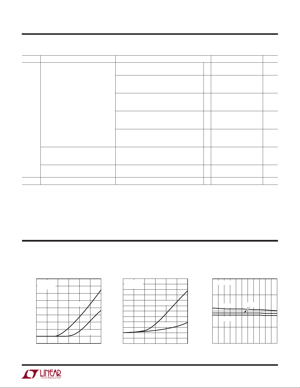
TYPICAL PERFORMANCE CHARACTERISTICS
Output Voltage vs Output Current
0
TA = 25°C
–0.25
–0.50
–0.75
–1.00
–1.25
–1.50
OUTPUT VOLTAGE (V)
–1.75
–2.00
–2.25
= –2V
V
OUT
0
VCC = 2.7V
V
= 3V
CC
1052515 30
OUTPUT CURRENT (mA)
20
1261L G01
–3.0
TA = 25°C
–3.1
V
= –4V
OUT
–3.2
–3.3
–3.4
–3.5
–3.6
–3.7
–3.8
OUTPUT VOLTAGE (V)
–3.9
–4.0
–4.1
–4.2
0
5
OUTPUT CURRENT (mA)
VCC = 4.5V
VCC = 5V
10 15 20
(See Test Circuits)
–1.90
–1.95
–2.00
OUTPUT VOLTAGE (V)
–2.05
25 30
1261L G02
–2.10
Output Voltage vs Supply VoltageOutput Voltage vs Output Current
V
= –2V
OUT
TA = –40°C
T
= 85°C
A
2.5 3.0 3.5 4.0 4.5 5.0
TA = 25°C
SUPPLY VOLTAGE (V)
1261L G03
3
LTC1261L
TEMPERATURE (°C)
–55
1.21
REFERENCE VOLTAGE (V)
1.22
1.23
1.24
1.25
–35 –15 5 25
1261L G09
45 65 85 105 125
VCC = 5V
ADJ = 0V
TEMPERATURE (°C)
–40
SHORT-CIRCUIT CURRENT (mA)
80
100
120
80
1261L G12
60
40
0
–10
20
50
–25 95
5
35
65
20
160
140
VCC = 5.25V
VCC = 5V
VCC = 3V
VCC = 2.7V
W
U
TYPICAL PERFORMANCE CHARACTERISTICS
(See Test Circuits)
Output Voltage vs Supply Voltage
–3.85
V
= –4V
OUT
–3.90
–3.95
–4.00
–4.05
OUTPUT VOLTAGE (V)
–4.10
–4.15
4.5
TA = –40°C
TA = 85°C
4.7 4.9
4.6 4.8
SUPPLY VOLTAGE (V)
TA = 25°C
5.0
Supply Current vs Supply Voltage
3.0
V
= –2V
OUT
= 0
I
OUT
2.5
2.0
1.5
= 85°C
T
1.0
SUPPLY CURRENT (mA)
0.5
0
A
TA = –40°C
3.0 3.5 4.0 4.5
SUPPLY VOLTAGE (V)
5.1
TA = 25°C
5.2
1261L G04
5.02.5
1261L G07
5.3
Minimum Required V
vs V
and I
OUT
5.6
5.2
4.8
4.4
4.0
3.6
3.2
2.8
POSITIVE SUPPLY VOLTAGE (V)
2.4
2.0
–5
5.0
V
= –4.5V
OUT
4.5
I
= 0
OUT
4.0
3.5
3.0
2.5
2.0
1.5
SUPPLY CURRENT (mA)
1.0
0.5
0
4.5
4.6 4.8
OUT
I
OUT
I
= 5mA I
OUT
–4 –3 0
OUTPUT VOLTAGE (V)
T
= 25°C
A
T
= –40°C
A
4.7
4.9
SUPPLY VOLTAGE (V)
CC
= 20mA
OUT
–2 –1
TA = 85°C
5.0
= 10mA
5.1
1261L G05
5.2
1261L G08
5.3
Maximum Output Current
vs Supply Voltage
80
TA = 25°C
70
60
50
40
30
20
MAXIMUM OUTPUT CURRENT (mA)
10
0
2.7
3.0 5.4
V
= –2V
OUT
V
= –3V
OUT
3.3
3.9
3.6
SUPPLY VOLTAGE (V)
V
4.2
Reference Voltage
vs TemperatureSupply Current vs Supply Voltage
OUT
= –4V
4.5
4.8
5.1
1261L G06
Oscillator Frequency
vs Temperature
725
TA = 25°C
V
OUT
700
V
CC
675
650
625
600
575
OSCILLATOR FREQUENCY (kHz)
550
525
–40
–25 95
4
= –4V
= 5V
–10
20
5
TEMPERATURE (°C)
35
Output Short-Circuit Current
vs TemperatureStart-Up Time vs Supply Voltage
0.7
TA = 25°C
= 10mA
I
OUT
0.6
0.5
V
= –4V
= –2V
3.5
OUT
4.0
4.5
5.0
1261L G11
0.4
0.3
0.2
START-UP TIME (ms)
0.1
80
50
65
1261L G10
0
2.5
V
OUT
3.0
SUPPLY VOLTAGE (V)
 Loading...