

Linear Technology LTC1250 Datasheet
LTC1250
Very Low Noise
Zero-Drift Bridge Amplifier
EATU
F
■
Very Low Noise: 0.75µV
■
DC to 1Hz Noise Lower Than OP-07
■
Full Output Swing into 1k Load
■
Offset Voltage: 10µV Max
■
Offset Voltage Drift: 50nV/°C Max
■
Common-Mode Rejection Ratio: 110dB Min
■
Power Supply Rejection Ratio: 115dB Min
■
No External Components Required
■
Pin-Compatible with Standard 8-Pin Op Amps
PPLICATI
A
■
Electronic Scales
■
Strain Gauge Amplifiers
■
Thermocouple Amplifiers
■
High Resolution Data Acquisition
■
Low Noise Transducers
■
Instrumentation Amplifiers
RE
S
O
U
S
Typ, 0.1Hz to 10Hz
P-P
DUESCRIPTIO
The LTC®1250 is a high performance, very low noise zerodrift operational amplifier. The LTC1250’s combination of
low front-end noise and DC precision makes it ideal for use
with low impedance bridge transducers. The LTC1250
features typical input noise of 0.75µV
10Hz, and 0.2µ V
DC to 1Hz noise of 0.35µ V
from 0.1Hz to 1Hz. The LTC1250 has
P-P
, surpassing that of low noise
P-P
bipolar parts including the OP-07, OP-77, and LT1012.
The LTC1250 uses the industry-standard single op amp
pinout, and requires no external components or nulling
signals, allowing it to be a plug-in replacement for bipolar
op amps.
The LTC1250 incorporates an improved output stage
capable of driving 4.3V into a 1k load with a single 5V
supply; it will swing ±4.9V into 5k with ±5V supplies. The
input common mode range includes ground with single
power supply voltages above 12V. Supply current is 3mA
with a ±5V supply, and overload recovery times from
positive and negative saturation are 0.5ms and 1.5ms,
respectively. The internal nulling clock is set at 5kHz for
optimum low frequency noise and offset drift; no external
connections are necessary.
from 0.1Hz to
P-P
and LTC are registered trademarks and LT is a trademark of Linear Technology Corporation.
U
O
A
PPLICATITYPICAL
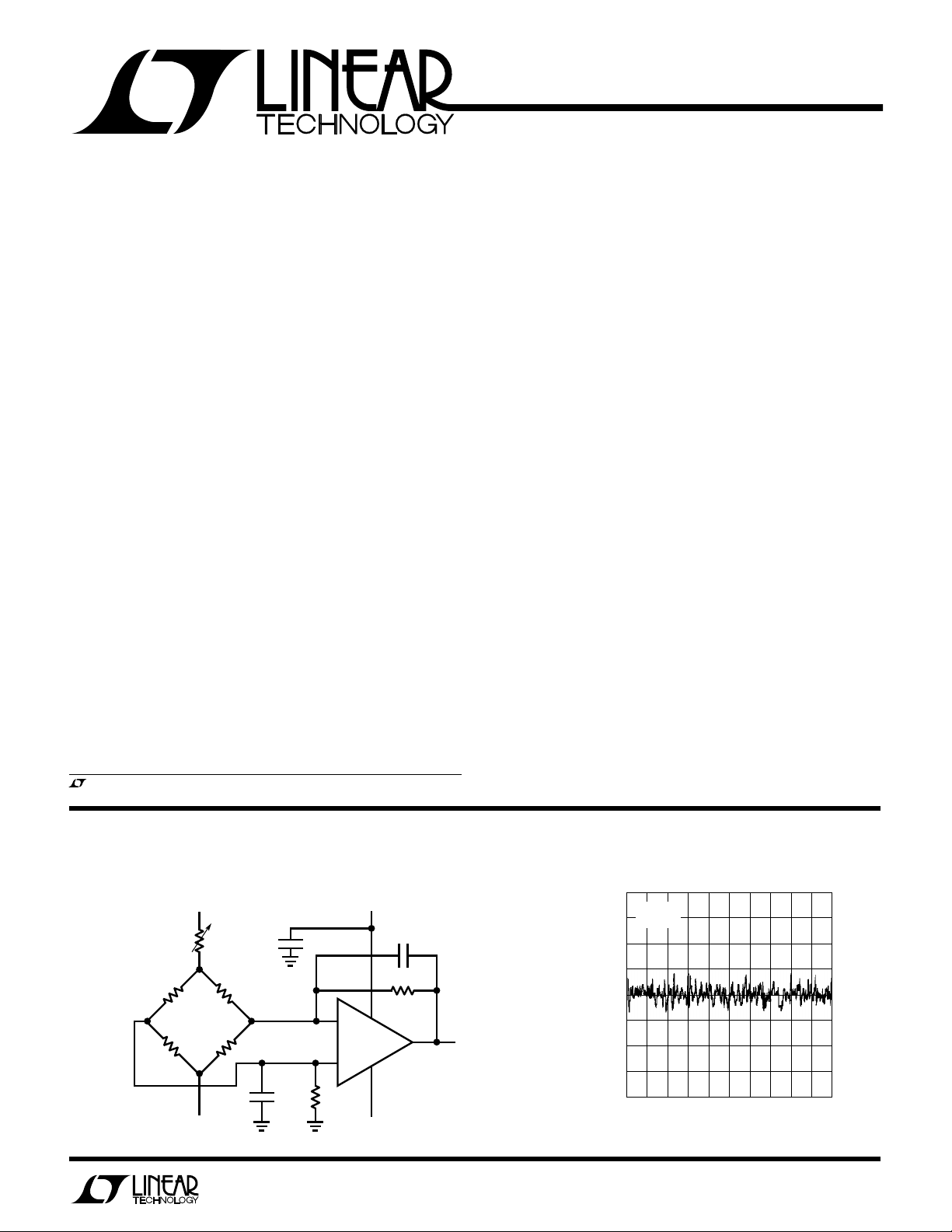
Differential Bridge Amplifier
2
3
18.2k
–
LTC1250
+
5V
1000pF
18.2k
7
6
4
–5V
5V
350Ω
STRAIN
GAUGE
–5V
50Ω
GAIN
TRIM
0.1µF
1000pF
The LTC1250 is available in standard 8-pin ceramic and
plastic DIPs, as well as an 8-pin SOIC package.
Input Referred Noise 0.1Hz to 10Hz
2
VS = ±5V
= 10k
A
V
1
0
µV
A
= 100
V
1250 TA01
–2
–1
2
0
4
TIME (s)
6
8
10
LT1250 TA02
1
LTC1250
W
O
A
LUTEXI T
S
Total Supply Voltage (V+ to V–) ............................. 18V
Input Voltage ........................ (V+ + 0.3V) to (V– – 0.3V)
Output Short Circuit Duration ......................... Indefinite
Operating Temperature Range
LTC1250M..................................... – 55°C to 125°C
LTC1250C .......................................... 0°C TO 70°C
Storage Temperature Range ................ –65°C to 150°C
Lead Temperature (Soldering, 10 sec.)................ 300°C
LECTRICAL C CHARA TERIST
E
SYMBOL PARAMETER CONDITIONS MIN TYP MAX MIN TYP MAX UNITS
V
OS
∆V
e
n
i
n
I
B
I
OS
CMRR Common-Mode Rejection Ratio VCM = –4V to 3V ● 110 130 110 130 dB
PSRR Power Supply Rejection Ratio VS = ±2.375V to ±8V ● 115 130 115 130 dB
A
VOL
SR Slew Rate RL = 10k, CL = 50pF 10 10 V/µs
GBW Gain-Bandwidth Product 1.5 1.5 MHz
I
S
f
S
Input Offset Voltage TA = 25°C (Note 1) ±5 ±10 ±5 ±10 µV
Average Input Offset Drift (Note 1) ● ±0.01 ±0.05 ±0.01 ±0.05 µV/°C
OS
Long Term Offset Drift 50 50 nV/√Mo
Input Noise Voltage (Note 2) TA = 25°C, 0.1Hz to 10Hz 0.75 1.0 0.75 1.0 µV
Input Noise Current f = 10Hz 4.0 4.0 fA/√Hz
Input Bias Current TA = 25°C (Note 3) ±50 ±150 ±50 ±200 pA
Input Offset Current TA = 25°C (Note 3) ±100 ±300 ±100 ±400 pA
Large-Signal Voltage Gain RL = 10k, V
Maximum Output Voltage Swing R
Supply Current No Load, TA = 25°C 3.0 4.0 3.0 4.0 mA
Internal Sampling Frequency TA = 25°C 4.75 4.75 kHz
A
WUW
ARB
TA = 25°C, 0.1Hz to 1Hz 0.2 0.2 µV
= 1k ● ±4.0 4.3/–4.7 ±4.0 4.3/–4.7 V
L
RL = 100k ±4.92 ±4.95 V
U
/
G
S
I
ICS
VIN = ±5V, TA = Operating Temperature Range, unless otherwise noted.
= ±4V ● 125 170 125 170 dB
OUT
PACKAGE
NC
1
–IN
2
+IN
3
–
V
4
J8 PACKAGE
8-LEAD CERAMIC DIP
8-LEAD PLASTIC SOIC
T
JMAX
T
JMAX
T
JMAX
● ±950 ±450 pA
● ±500 ±500 pA
● 7.0 5.0 mA
O
RDER I FOR ATIO
TOP VIEW
NC
8
+
V
7
OUT
6
NC
5
N8 PACKAGE
8-LEAD PLASTIC DIP
S8 PACKAGE
= 150°C, θJA = 100°CW (J8)
= 110°C, θJA = 130°CW (N8)
= 110°C, θJA = 200°CW (S8)
LTC1250M LTC1250C
S8 PART MARKING
WU
ORDER PART
NUMBER
LTC1250MJ8
LTC1250CJ8
LTC1250CN8
LTC1250CS8
1250
U
P-P
P-P
VIN = 5V, TA = Operating Temperature Range, unless otherwise noted.
LTC1250M LTC1250C
SYMBOL PARAMETER CONDITIONS MIN TYP MAX MIN TYP MAX UNITS
V
∆V
e
I
I
OS
n
B
OS
Input Offset Voltage TA = 25°C (Note 1) ±2 ±5 ±2 ±5 µV
Average Input Offset Drift (Note 1) ● ±0.01 ±0.05 ±0.01 ±0.05 µV/°C
OS
Input Noise Voltage (Note 2) TA = 25°C, 0.1Hz to 10Hz 1.0 1.0 µV
TA = 25°C, 0.1Hz to 1Hz 0.3 0.3 µV
Input Bias Current TA = 25°C (Note 3) ±20 ±100 ±20 ±100 pA
Input Offset Current TA = 25°C (Note 3) ±40 ±200 ±40 ±200 pA
P-P
P-P
2
LTC1250
TEMPERATURE (°C)
–50
SAMPLING FREQUENCY (kHz)
4
5
6
25
LTC1250 G06
3
2
–25 0 50
1
0
8
7
75 100 150
VS = ±5V
TOTAL SUPPLY VOLTAGE, V+ TO V– (V)
4
2
SAMPLING FREQUENCY (kHz)
3
4
681012
LTC1250 G03
5
6
14
16
TA = 25°C
LECTRICAL C CHARA TERIST
E
ICS
VIN = 5V, TA = Operating Temperature Range, unless otherwise noted.
LTC1250M LTC1250C
SYMBOL PARAMETER CONDITIONS MIN TYP MAX MIN TYP MAX UNITS
Maximum Output Voltage Swing R
= 1k 4.0 4.3 4.0 4.3 V
L
RL = 100k 4.95 4.95 V
I
S
f
S
The ● denotes specifications which apply over the full operating
temperature range.
Note 1: These parametes are guaranteed by design. Thermocouple effects
preclude measurement of these voltage levels during automated testing.
Supply Current TA = 25°C 1.8 2.5 1.8 2.5 mA
Sampling Frequency TA = 25°C 3 3 kHz
filter at 0.1Hz. The LTC1250 is sample tested for noise; for 100% tested
parts contact LTC Marketing Dept.
Note 3: At T ≤ 0°C these parameters are guaranteed by design and not
tested.
Note 2: 0.1Hz to 10Hz noise is specified DC coupled in a 10s window;
0.1Hz to 1Hz noise is specified in a 100s window with an RC high-pass
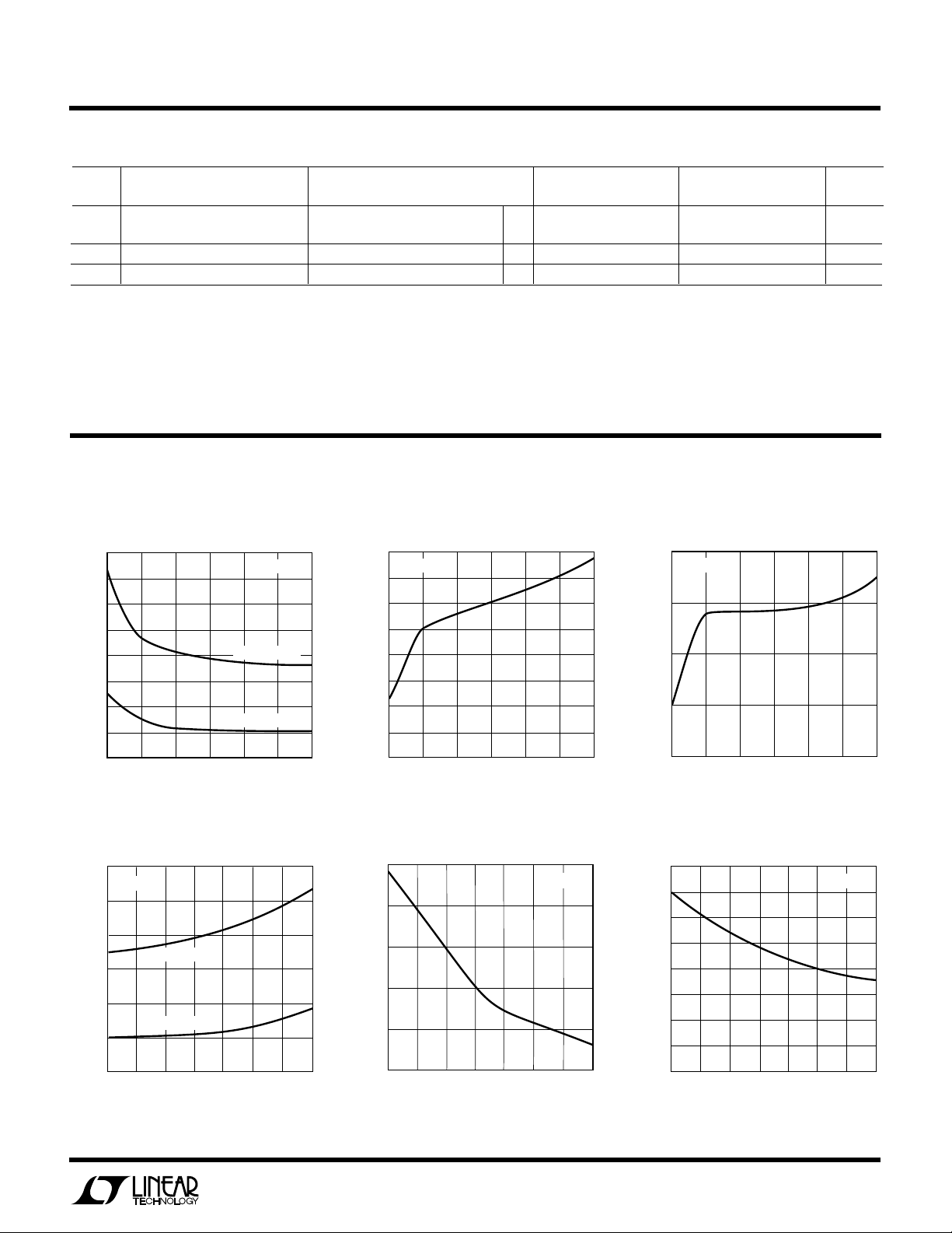
UW
LPER
F
O
Input Noise vs Supply Voltage
1.6
1.4
1.2
)
P-P
1.0
0.8
0.6
INPUT NOISE (µV
0.4
0.2
0
681012
4
TOTAL SUPPLY VOLTAGE, V+ TO V– (V)
R
TA = 25°C
0.1Hz TO 10Hz
0.1Hz TO 1Hz
14
LTC1250 G01
ATYPICA
CCHARA TERIST
E
C
Supply Current vs Supply Voltage
4.0
TA = 25°C
3.5
3.0
2.5
2.0
1.5
SUPPLY CURRENT (mA)
1.0
0.5
0
16
4
TOTAL SUPPLY VOLTAGE, V+ TO V– (V)
681012
ICS
14
LTC1250 G02
Sampling Frequency vs Supply
Voltage
16
1.2
VS = ±5V
1.0
)
P-P
0.8
0.6
0.4
INPUT NOISE (µV
0.2
0
–50
–25 0
0.1Hz TO 10Hz
0.1Hz TO 1Hz
25 75
TEMPERATURE (°C)
50 100 125
LTC1250 G04
Supply Current vs TemperatureInput Noise vs Temperature
4.5
4.0
3.5
3.0
SUPPLY CURRENT (mA)
2.5
2.0
–50
–25
0
TEMPERATURE (°C)
Sampling Frequency vs
Temperature
VS = ±5V
50
25
75
100
LTC1250 G05
125
3
 Loading...