

Linear Technology LTC1151 Datasheet
LTC1151
Dual ±15V Zero-Drift
Operational Amplifier
EATU
F
■
Maximum Offset Voltage Drift: 0.05µV/°C
■
High Voltage Operation: ±18V
■
No External Components Required
■
Maximum Offset Voltage: 5µV
■
Low Noise: 1.5µV
■
Minimum Voltage Gain: 125dB
■
Minimum CMRR: 106dB
■
Minimum PSRR: 110dB
■
Low Supply Current: 0.9mA/Amplifier
■
Single Supply Operation: 4.75V to 36V
■
Input Common-Mode Range Includes Ground
■
Typical Overload Recovery Time: 20ms
PPLICATI
A
■
Strain Gauge Amplifiers
■
Instrumentation Amplifiers
■
Electronic Scales
■
Medical Instrumentation
■
Thermocouple Amplifiers
■
High Resolution Data Acquisition
RE
S
(0.1Hz to 10Hz)
P-P
U
O
S
DUESCRIPTIO
The LTC1151 is a high voltage, high performance dual
zero-drift operational amplifier. The two sample-and-hold
capacitors per amplifier required externally by other chopper amplifiers are integrated on-chip. The LTC1151 also
incorporates proprietary high voltage CMOS structures
which allow operation at up to 36V total supply voltage.
The LTC1151 has a typical offset voltage of 0.5µV,
drift of 0.01µV/°C, 0.1Hz to 10Hz input noise voltage of
1.5µV
rate of 3V/µs and a gain-bandwidth product of 2.5MHz
with a supply current of 0.9mA per amplifier. Overload
recovery times from positive and negative saturation are
3ms and 20ms, respectively.
The LTC1151 is available in a standard 8-lead plastic DIP
package as well as a 16-lead wide body SO. The LTC1151
is pin compatible with industry-standard dual op amps
and runs from standard ±15V supplies, allowing it to plug
in to most standard bipolar op amp sockets while offering
significant improvement in DC performance.
, and a typical voltage gain of 140dB. It has a slew
P-P
A
PPLICATITYPICAL
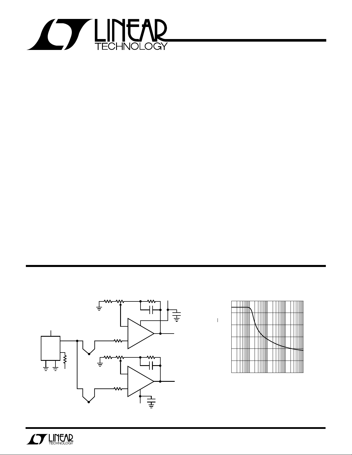
±15V Dual Thermocouple Amplifier
15V
7
V
IN
K
LT1025
GND
* FULL SCALE TRIM: TRIM FOR 10.0V OUTPUT
WITH THERMOCOUPLE AT 100°C
3
V
O
–
R
4
470k
5
–15V
–
–
+
51Ω 100Ω*
TYPE K
+
TYPE K
O
2k
2k
U
6
5
2
3
–
1/2
LTC1151
+
–
1/2
LTC1151
+
–15V
Noise Spectrum
7
1
0.1µF
15V
0.1µF
OUTPUT A
100mV/°C
OUTPUT B
100mV/°C
1151 TA01
60
50
40
30
20
NOISE VOLTAGE (nV/√Hz)
10
0
10
1 100 1k 10k
FREQUENCY (Hz)
1151 TA02
240k51Ω 100Ω*
0.1µF
8
240k
0.1µF
4
1
LTC1151
A
W
O
LUTEXI T
S
A
WUW
ARB
U
G
I
S
(Note 1)
Total Supply Voltage (V+ to V–) ............................. 36V
Input Voltage (Note 2) ..........(V+ + 0.3V) to (V– – 0.3V)
Output Short Circuit Duration ......................... Indefinite
Burn-In Voltage ...................................................... 36V
WU
/
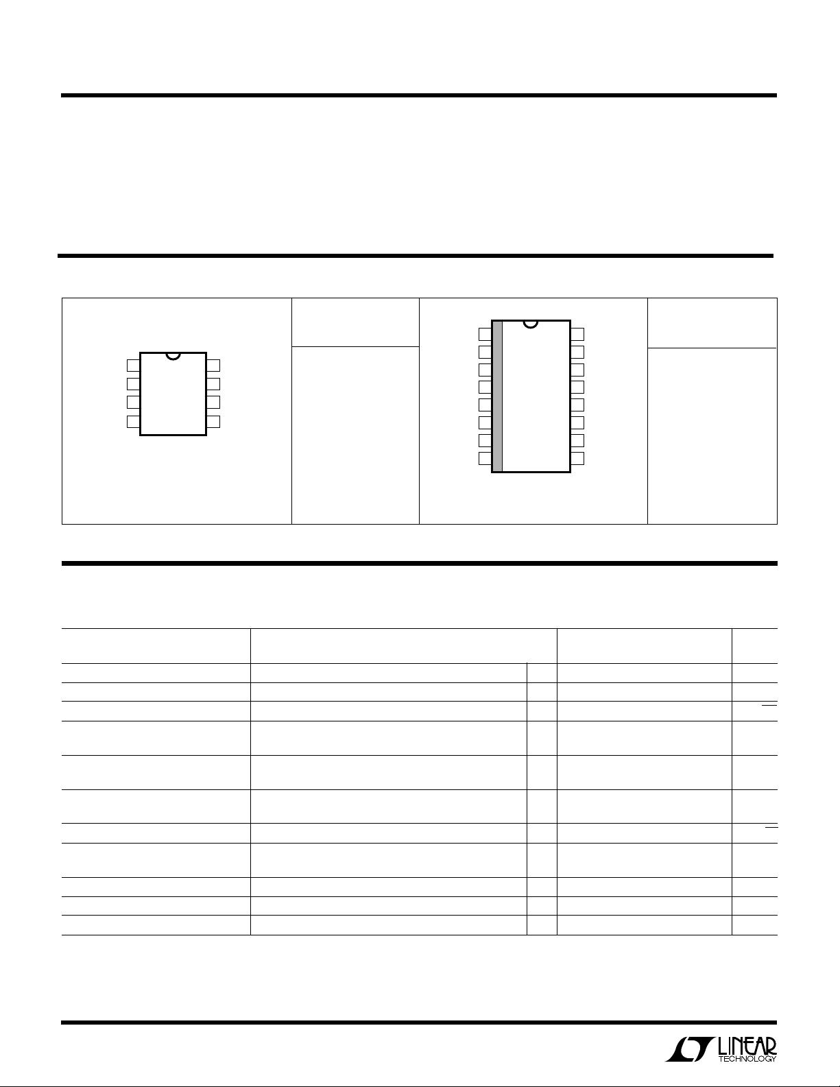
PACKAGE
OUT A
–IN A
+IN A
–
V
T
JMAX
O
RDER I FOR ATIO
TOP VIEW
1
2
3
4
N8 PACKAGE
8-LEAD PLASTIC DIP
= 110°C, θJA = 130°C/W
ORDER PART
NUMBER
V+
8
OUT B
7
–IN B
6
+IN B
5
LTC1151CN8
Operating Temperature Range
LTC1151C............................................... 0°C to 70°C
Storage Temperature Range ................ –65°C to 150°C
Lead Temperature (Soldering, 10 sec)................. 300°C
U
NC
NC
OUT A
–IN A
+IN A
NC
NC
1
2
3
4
5
–
V
6
7
8
T
JMAX
TOP VIEW
S PACKAGE
16-LEAD PLASTIC SOL
= 110°C, θJA = 200°C/W
NC
16
NC
15
+
V
14
OUT B
13
–IN B
12
+IN B
11
NC
10
NC
9
ORDER PART
NUMBER
LTC1151CS
LECTRICAL C CHARA TERIST
E
ICS
VS = ±15V, TA = Operating Temperature Range, unless otherwise specified.
LTC1151C
PARAMETER CONDITIONS MIN TYP MAX UNITS
Input Offset Voltage TA = 25°C (Note 3) ±0.5 ±5 µV
Average Input Offset Drift (Note 3) ● ±0.01 ±0.05 µV/°C
Long Term Offset Voltage Drift 50 nV/√mo
Input Offset Current T
Input Bias Current T
Input Noise Voltage R
Input Noise Current f = 10Hz (Note 4) 2.2 fA/√Hz
Input Voltage Range Positive
Common-Mode Rejection Ratio VCM = V– to 12V ● 106 130 dB
Power Supply Rejection Ratio VS = ±2.375V to ±16V ● 110 130 dB
Large-Signal Voltage Gain RL = 10k, V
= 25°C ±20 ±200 pA
A
= 25°C ±15 ±100 pA
A
= 100Ω, 0.1Hz to 10Hz 1.5 µV
S
RS = 100Ω, 0.1Hz to 1Hz 0.5 µV
Negative ● –15 –15.3 V
= ±10V ● 125 140 dB
OUT
● ±0.5 nA
● ±0.5 nA
P-P
P-P
● 12 13.2 V
2

LTC1151
LECTRICAL C CHARA TERIST
E
VS = ±15V, TA = Operating Temperature Range, unless otherwise specified.
PARAMETER CONDITIONS MIN TYP MAX UNITS
Maximum Output Voltage Swing R
Slew Rate RL = 10k, CL = 50pF 2.5 V/µs
Gain-Bandwidth Product 2 MHz
Supply Current per Amplifier No Load, T
Internal Sampling Frequency 1000 Hz
VS = 5V, TA = Operating Temperature Range, unless otherwise specified.
Input Offset Voltage TA = 25°C (Note 3) ±0.05 ±5 µV
Average Input Offset Drift (Note 3) ● ±0.01 ±0.05 µV/°C
Long Term Offset Voltage Drift 50 nV/√mo
Input Offset Current TA = 25°C ±10 100 pA
Input Bias Current TA = 25°C ±550 pA
Input Noise Voltage R
Input Noise Current f = 10Hz (Note 4) 1.3 fA/√Hz
Input Voltage Range Positive 2.7 3.2 V
Common-Mode Rejection Ratio VCM = 0V to 2.7V 110 dB
Power Supply Rejection Ratio VS = ±2.375V to ±16V ● 110 130 dB
Large-Signal Voltage Gain RL = 10k, V
Maximum Output Voltage Swing R
Slew Rate RL = 10k, CL = 50pF 1.5 V/µs
Gain Bandwidth Product 1.5 MHz
Supply Current per Amplifier No Load, T
Internal Sampling Frequency 750 Hz
= 10k, TA = 25°C ±13.5 ±14.50 V
L
= 10k ● +10.5/–13.5 V
R
L
RL = 100k ±14.95 V
No Load ● 2.0 mA
= 100Ω, 0.1Hz to 10Hz 2.0 µV
S
RS = 100Ω, 0.1Hz to 1Hz 0.7 µV
Negative 0 – 0.3 V
= 10k to GND 4.85 V
L
RL = 100k to GND 4.97 V
ICS
LTC1151C
= 25°C 0.9 1.5 mA
A
= 0.3V to 4.5V ● 115 140 dB
OUT
= 25°C 0.5 1.0 mA
A
● 1.5 mA
P-P
P-P
The • denotes the specifications which apply over the full operating
temperature range.
Note 1: Absolute Maximum Ratings are those values beyond which life of
the device may be impaired.
Note 2: Connecting any terminal to voltages greater than V
–
may cause destructive latch-up. It is recommended that no sources
V
operating from external supplies be applied prior to power-up of the
LTC1151.
+
or less than
Note 3: These parameters are guaranteed by design. Thermocouple
effects preclude measurement of these voltage levels in high speed
automatic test systems. V
equipment capability.
Note 4: Current Noise is calculated from the formula:
IN = √(2q • Ib)
where q = 1.6 × 10
–19
is measured to a limit determined by test
OS
Coulomb.
3
 Loading...