

Linear Technology LT1032 Datasheet
FEATURES
LT1032
Quad Low Power
Line Driver
U
DESCRIPTIO
■
Low Operating Voltage: ±5V to ±15V
■
500µA Supply Current
■
Zero Supply Current when Shut Down
■
Outputs Can Be Driven ±30V
■
Thermal Limiting
■
Output “Open” when Off (Three-State)
■
10mA Output Drive
■
Pinout Similar to 1488
U
APPLICATIO S
■
RS232
■
Power Supply Inverter
■
Micropower Interface
■
Level Translator
The LT®1032 is a RS232 and RS423 line driver that
operates over a ±5V to ±15V range on low supply current
and can be shut down to zero supply current. Outputs are
fully protected from externally applied voltages of ±30V by
both current and thermal limiting. Since the output swings
to within 200mV of the positive supply and 600mV of the
negative supply, power supply needs are minimized.
Also included is a strobe pin to force all outputs low
independent of input or shutdown conditions. Further,
slew rate can be adjusted with a resistor connected to the
supply.
A major advantage of the LT1032 is the high impedance
output state when off or powered down.
For applications requiring dual or triple RS232 driver/
receiver devices, see the LT1180A (dual), LT1039A (triple)
or the LT1130A data sheets.
, LTC and LT are registered trademarks of Linear Technology Corporation.
TYPICAL APPLICATIO
RS232 Line Driver
1
–6V
INPUT
OUTPUT
ON/OFF
(0V TO 5V)
†
INPUT
OUTPUT
GND
*NO CONNECTION NEEDED WHEN NOT USED
†
5V = ON
LT1032
2
3
4
5
6
7
U
14
6V
13
STROBE*
12
INPUT
11
OUTPUT
10
RESPONSE TIME
CONTROL*
9
INPUT
8
OUTPUT
LT1032 • TA01
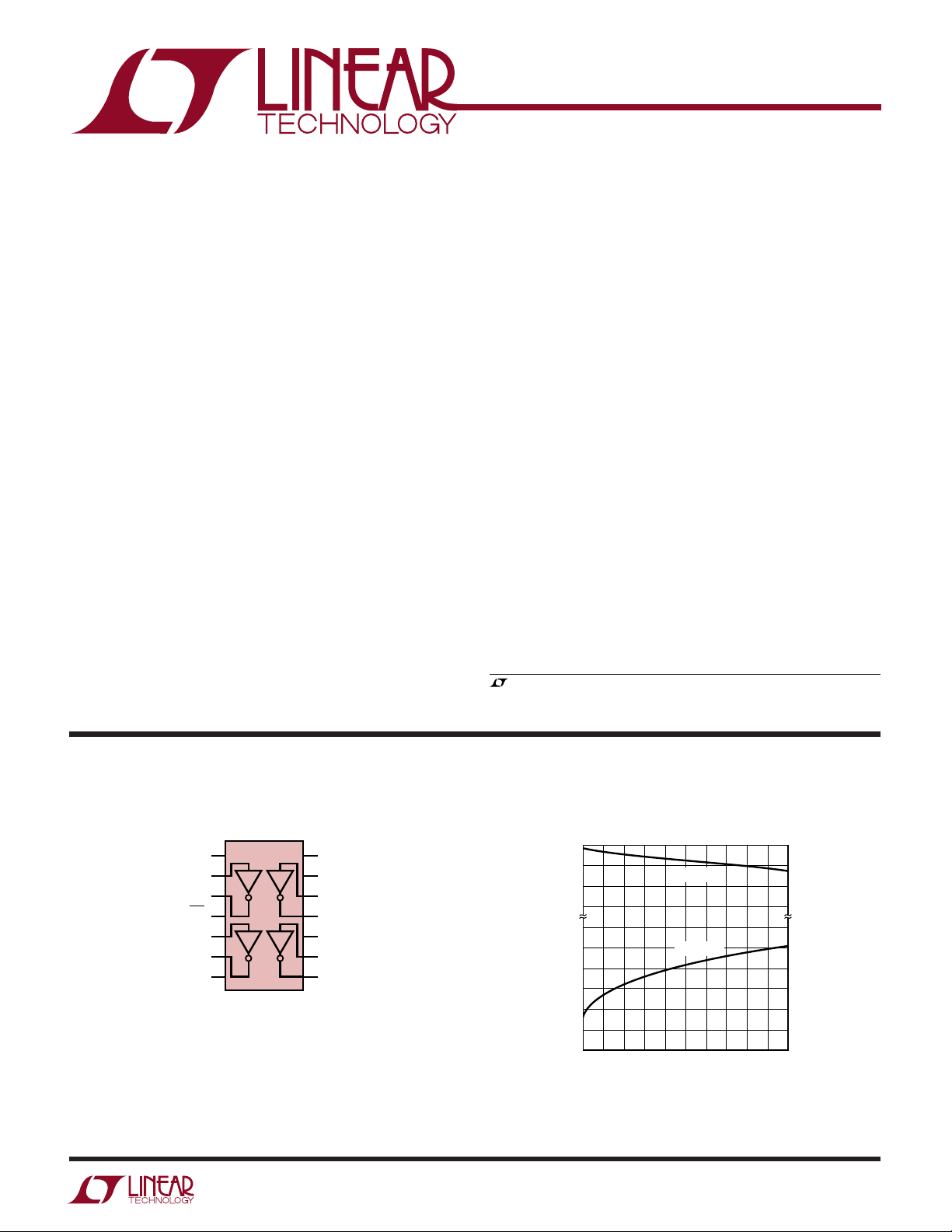
Output Swing vs Output Current
+
V
0.2
0.4
1.0
0.8
0.6
0.4
0.2
–
OUTPUT VOLTAGE REFERRED TO SUPPLIES (V)
V
2
0
V
HIGH
OUT
V
LOW
OUT
6
4
OUTPUT CURRENT (mA)
8
10
LT1032 • TA02
1
LT1032
TOP VIEW
SW PACKAGE
16-LEAD PLASTIC SO (WIDE)
1
2
3
4
5
6
7
8
16
15
14
13
12
11
10
9
V
EE
ON/OFF
GND
NC
V
CC
STROBE
NC
RESPONSE
CONTROL
A
W
O
LUTEXI TIS
S
A
WUW
U
(Note 1)
ARB
G
Supply Voltage ..................................................... ±15V
Logic Input Pins ............................................ V– to 25V
ON/OFF Pin ................................................. GND to 15V
Output (Forced) ............................. V– + 30V, V+ – 30V
Response Pin ......................................................... ±6V
Short-Circuit Duration (to ±30V) .................... Indefinite
Storage Temperature Range ................ –65°C to 150°C
WU
/
1
2
3
4
5
6
7
O
RDER I FOR ATIO
TOP VIEW
V
CC
14
(5V TO 15V)
STROBE
13
12
11
RESPONSE
10
CONTROL
9
8
N PACKAGE
14-LEAD PDIP
ORDER PART
NUMBER
LT1032CJ
LT1032CN
LT1032IN
LT1032MJ
PACKAGE
V
EE
(–15V TO – 5V)
ON/OFF
(0V TO 5V)
GND
J PACKAGE
14-LEAD CERDIP
T
= 85°C, θJA = 100°C/W, θJC = 60°C (CJ)
JMAX
= 85°C, θJA = 100°C/W, θJC = 60°C (CN)
T
JMAX
= 150°C, θJA = 100°C/W, θJC = 60°C (MJ)
T
JMAX
Operating Temperature Range
LT1032C............................................... 0°C to 70°C
LT1032I........................................... – 40°C to 85°C
LT1032M....................................... – 55°C to 125°C
C Grade Guaranteed
Functional by Design .............................. –25°C to 85°C
Lead Temperature (Soldering, 10 sec)................. 300°C
U
ORDER PART
NUMBER
LT1032CSW
LT1032ISW
T
= 85°C, θJA = 80°C/W
JMAX
LECTRICAL C CHARA TERIST
E
The ● denotes specifications which apply over the full operating temperature
ICS
range, otherwise specifications are at TA = 25°C. Supply voltage = ±5V to ±15V
PARAMETER CONDITIONS MIN TYP MAX UNITS
Supply Current V
Power Supply Leakage Current V
Output Voltage Swing Load = 2mA Positive V+ – 0.3V V+ – 0.1V V
Output Current (Active) V
Output Current (Shutdown) V
Output Overload Voltage (Forced) Operating or Shutdown ● V+ – 30V V– + 30V V
Input Overload Voltage (Forced) Operating of Shutdown ● V
Logic Input Levels Low Input (V
Logic Input Current VIN > 2.0V 2 20 µA
ON/OFF Pin Current 0 ≤ VIN ≤ 5V ● –10 3 50 µA
Slew Rate I
Change in Slew Rate (Note 3) I
Response Pin Leakage V
Note 1: Absolute Maximum Ratings are those values beyond which the life
of a device may be impaired.
Note 2: 3V applied to the strobe pin will force all outputs low. Strobe pin
input impedance is about 2k to ground. Leave open when not used.
2
≥ 2.4V, I
ON/OFF
≤ 0.4V 1 10 µA
ON/OFF
≤ 0.1V, TA = 125°C ● 10 50 µA
V
ON/OFF
= ±5V to ±15V 10 22 mA
SUPPLY
= 0V, V
SUPPLY
V
= ±15V, V
SUPPLY
High Input (V
V
< 0.8V 10 20 µA
IN
RESPONSE
RESPONSE
I
RESPONSE
V
= 0, RL = 3k 4 15 30 V/µs
= 50µA 50 %
= –50µA–50%
= ±6V, V
SUPPLY
RESPONSE
= ±6V
= 0, All Outputs Low ● 500 1000 µA
OUT
Negative V
= ±30V 2 100 µA
OUT
= ±20V 2 100 µA
OUT
–
= High) ● 1.4 0.8 V
OUT
= Low) ● 2 1.4 V
OUT
≤ 0.4V 1 µA
ON/OFF
Note 3: Response can be changed by connecting a resistor to the supply.
For supplies less than ±6V this current is disconnected when shut down.
Leave open when not used.
–
+ 0.7V V– + 0.9V V
30V V
LPER
F
O
R
ATYPICA
UW
CCHARA TERIST
E
C
LT1032
ICS
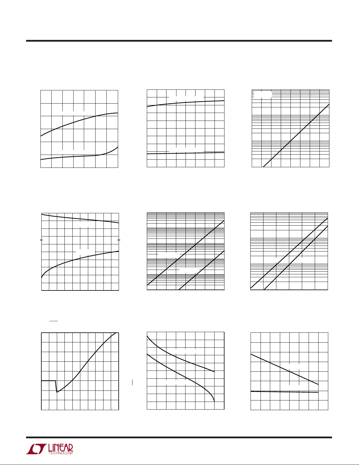
On Supply Current
vs Temperature
3.0
2.5
2.0
1.5
1.0
SUPPLY CURRENT (mA)
0.5
0
–50
ALL OUTPUTS HIGH
ALL OUTPUTS LOW
–25 0
50 100 125
25 75
TEMPERATURE (˚C)
LT1032 • TPC01
Output Swing vs Output Current
+
V
0.2
0.4
1.0
0.8
0.6
0.4
0.2
–
OUTPUT VOLTAGE REFERRED TO SUPPLIES (V)
V
2
0
V
HIGH
OUT
V
LOW
OUT
6
4
OUTPUT CURRENT (mA)
8
LT1032 • TA02
10
Supply Current
vs Supply Voltage
2.0
1.8
1.6
1.4
1.2
1.0
0.8
0.6
SUPPLY CURRENT (mA)
0.4
0.2
0
5
ALL OUTPUTS HIGH
ALL OUTPUTS LOW
7.5
10
SUPPLY VOLTAGE (±V)
Output Leakage vs Temperature
100µA
10µA
1µA
V
= –30V
100nA
OUTPUT CURRENT
10nA
1nA
OUT
V
= 30V
OUT
25 75 100
50
TEMPERATURE (°C)
12.5
LT1032 • TPC02
LT1032 • TPC05
125
Off Supply Current
vs Temperature
1000
VS = ±12V
100
10
SUPPLY CURRENT (nA)
1
15
25
50 100 125
75
TEMPERATURE (°C)
LT1032 • TPC03
Response Pin Leakage
vs Temperature (Device Off)
1000
100
10
RESPONSE PIN LEAKAGE (µA)
1
25
V = 5V V = –5V
50 75 100
TEMPERATURE (°C)
LT1032 • G06
ON/OFF Pin Current vs Voltage
10
8
6
4
2
0
CURRENT (µA)
–2
–4
–6
1
0
INPUT VOLTAGE (V)
3
2
4
LT1032 • TPC07
Shutdown Pin Voltage
vs Temperature
2.0
1.8
1.6
1.4
1.2
1.0
0.8
0.6
ON/OFF PIN VOLTAGE (V)
0.4
0.2
0
–50
5
–25 25
MIN ON VOLTAGE
MAX OFF VOLTAGE
0
50
TEMPERATURE (°C)
125
100
75
150
LT1032 • TPC08
Current Limit vs Temperature
80
70
60
50
40
30
OUTPUT CURRENT (mA)
20
10
0
–25
–55
SINKING
SOURCING
0
50
25
TEMPERATURE (°C)
75
100
125
LT1032 • TPC09
150
3
 Loading...