


TEMPERATURE (°C)
–50
OUTPUT VOLTAGE (V)
5.002
5.004
5.006
25 75
1027 TA02
5.000
4.998
–25 0
50 100
4.996
4.994
FEATURES
LT1027
Precision
5V Reference
U
DESCRIPTIO
■
Very Low Drift: 2ppm/°C Max TC
■
Pin Compatible with LT1021-5, REF-02,
(TO-5 and PDIP Packages Only)
■
Output Sources 15mA, Sinks 10mA
■
Excellent Transient Response Suitable for
A-to-D Reference Inputs
■
Noise Reduction Pin
■
Excellent Long Term Stability
■
Less Than 1ppm
Noise (0.1Hz to 10Hz)
P-P
U
APPLICATIO S
■
A-to-D and D-to-A Converters
■
Digital Voltmeters
■
Reference Standard
■
Precision Current Source
U
TYPICAL APPLICATIO
The LT®1027 is a precision reference with extra-low drift,
superior accuracy, excellent line and load regulation and
low output impedance at high frequency. This device is
intended for use in 12- to 16-bit A-to-D and D-to-A
systems where demanding accuracy requirements must
be met without the use of power hungry, heated substrate
references. The fast settling output recovers quickly from
load transients such as those presented by A-to-D converter
reference inputs. The LT1027 brings together both
outstanding accuracy and temperature coefficient
specifications.
The LT1027 reference is based on LTC’s proprietary
advanced subsurface Zener bipolar process which
eliminates noise and stability problems associated with
surface breakdown devices.
, LTC and LT are registered trademarks of Linear Technology Corporation.
+
Supplying V
8V TO 40V
2.2µF
REF
V
IN
V
OUT
LT1027
V
TRIM
GND
and VCC to the LTC®1290 12-bit ADC
V
CC
S
CLK
A
CLK
D
OUT
D
CS
–
DGND
V
ANALOG
INPUTS
+
10k 22µF
CH0
CH1
CH2
CH3
CH4
CH5
CH6
CH7
COM
REF
REF
AGND
LTC1290
+
–
Output Voltage
TO µC
IN
1027 TA01
1
LT1027
A
W
O
LUTEXI TIS
S
A
WUW
U
(Note 1)
ARB
G
Supply Voltage (VIN)............................................... 40V
Input-Output Voltage Differential ............................ 35V
Output to Ground Voltage ......................................... 7V
V
to Ground Voltage
TRIM
Positive ................................................................ 5V
Negative .......................................................... –0.3V
Output Short-Circuit Duration
VIN > 20V........................................................ 10 sec
VIN ≤ 20V ................................................... Indefinite
WU
/
PACKAGE
V
IN
T
= 150°C, θJA = 150°C/W, θJC = 45°C/W
JMAX
O
RDER I FOR ATIO
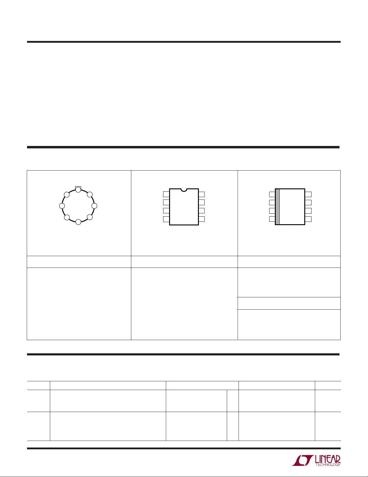
TOP VIEW
NC*
8
1
NC*
2
3
NR
H PACKAGE
8-LEAD TO-5 METAL CAN
7
5
4
GND
6
NC*
V
V
TRIM
OUT
1
NC*
2
V
IN
3
NR
4
GND
N8 PACKAGE
8-LEAD PDIP
T
= 100°C, θJA = 130°C/W T
JMAX
Operating Temperature Range
LT1027C................................................ 0°C to 70°C
LT1027M ......................................... –55°C to 125°C
Storage Temperature Range
All Devices....................................... – 65°C to 150°C
Lead Temperature (Soldering, 10 sec)................. 300°C
U
TOP VIEW
V
GND
TRIM
V
NR
OUT
8
NC*
NC*
7
V
6
OUT
V
5
TRIM
TOP VIEW
1
2
3
4
S8 PACKAGE
8-LEAD PLASTIC SO
= 100°C, θJA = 180°C/W
JMAX
8
V
IN
NC*
7
NC*
6
NC*
5
ORDER PART NUMBER ORDER PART NUMBER
LT1027ACH-5
LT1027BCH-5
LT1027CCH-5
LT1027DCH-5
LT1027BCN8-5
LT1027CCN8-5
LT1027DCN8-5
LT1027ECN8-5
LT1027ECH-5
ORDER PART NUMBER
LT1027CCS8-5
LT1027DCS8-5
LT1027ECS8-5
S8 PART MARKING
1027C5
1027D5
1027E5
*Connected internally. Do not connect external circuitry to these pins. Consult factory for Industrial and Military grade parts.
LECTRICAL C CHARA TERIST
E
temperature range otherwise specifications are at TA = 25°C. VIN = 10V, I
SYMBOL PARAMETER CONDITIONS MIN TYP MAX UNITS
V
OUT
TCV
OUT
Output Voltage (Note 2) LT1027A 4.9990 5.000 5.0010 V
Output Voltage Temperature Coefficient LT1027A, B ● 1 2 ppm/°C
(Note 3) LT1027C
The ● denotes specifications which apply over the full operating
ICS
= 0, unless otherwise specified.
LOAD
LT1027B, C, D 4.9975 5.000 5.0025
LT1027E 4.9950 5.000 5.0050
● 23
LT1027D
LT1027E
● 25
● 3 7.5
2

LT1027
TEMPERATURE (°C)
–50
OUTPUT VOLTAGE (V)
5.002
5.004
5.006
25 75
1027 G03
5.000
4.998
–25 0
50 100
4.996
4.994
LECTRICAL C CHARA TERIST
E
temperature range otherwise specifications are at TA = 25°C. VIN = 10V, I
SYMBOL PARAMETER CONDITIONS MIN TYP MAX UNITS
Line Regulation (Note 4) 8V ≤ VIN ≤ 10V 6 12 ppm/V
Load Regulation (Notes 4, 6) Sourcing Current –8 –3 6 ppm/mA
Supply Current 2.2 2.7 mA
V
Adjust Range ● ±30 ±50 mV
TRIM
e
n
Note 1: Absolute Maximum Ratings are those values beyond which the life
of the part may be impaired.
Note 2: Output voltage is measured immediately after turn-on. Changes
due to chip warm-up are typically less than 0.005%.
Note 3: Temperature coefficient is determined by the "box" method in
which the maximum ∆V
Note 4: Line and load regulation measurements are done on a pulse basis.
Output voltage changes due to die temperature change must be taken into
account separately. Package thermal resistance is 150°C/W for TO-5 (H),
130°C/W for PDIP (N8), and 180°C/W for plastic SO (SO-8).
Output Noise (Note 5) 0.1Hz ≤ f ≤ 10Hz 3 µV
Temperature Hysteresis H package; ∆T = 25°C 10 ppm
Long Term Stability H package 20 ppm/month
over the temperature range is divided by ∆T.
OUT
The ● denotes specifications which apply over the full operating
ICS
= 0, unless otherwise specified.
LOAD
● 25 ppm/V
10V ≤ VIN ≤ 40V 3 6 ppm/V
● 8 ppm/V
≤ 15mA ● – 10 8 ppm/mA
0 ≤ I
OUT
Sinking Current 30 50 ppm/mA
0 ≥ I
≥ –10mA ● 100 ppm/mA
OUT
● 3.1 mA
10Hz ≤ f ≤ 1kHz 2.0 6.0 µV
Note 5: RMS noise is measured with an 8-pole bandpass filter with a
center frequency of 30Hz and a Q of 1.5. The filter output is then rectified
and integrated for a fixed time period, resulting in an average, as opposed
to RMS voltage. A correction factor is used to convert average to RMS.
This value is then used to obtain RMS noise voltage in the 10Hz to 1000Hz
frequency band. This test also screens for low frequency "popcorn" noise
within the bandwidth of the filter. Consult factory for 100% 0.1Hz to 10Hz
noise testing.
Note 6: Devices typically exhibit a slight negative DC output impedance of
–0.015Ω. This compensates for PC trace resistance, improving regulation
at the load.
P-P
RMS
100
120
110
100
90
80
REJECTION (dB)
70
60
50
LPER
Ripple Rejection
VIN = 10V
10
100 1k 10k
FREQUENCY (Hz)
F
O
R
ATYPICA
1027 G01
UW
CCHARA TERIST
E
C
Output Impedance vs Frequency
100
∆I = ±3mA AC
= 5mA
I
SOURCE
10
1
0.1
OUTPUT IMPEDANCE (Ω)
0.01
10
100
1k
FREQUENCY (Hz)
10k
ICS
100k
Output Voltage
1M
1027 G02
3

LT1027
FREQUENCY (Hz)
10
80
100
120
140
160
100 1k 10k
1027 G09
60
40
20
0
180
200
CNR = 1µF
CNR = 0
OUTPUT NOISE DENSITY (nV/√Hz)
LPER
UW
R
F
O
ATYPICA
CCHARA TERIST
E
C
ICS
Start-Up and Turn-Off (No Load)
V
OUT
1V/DIV
10V
V
IN
1µs/DIV
Load Regulation
800
400
0
–400
–800
–1200
CHANGE IN OUTPUT VOLTAGE (µV)
–1600
–10
–8 –6 –4 –2 0 10 12
264
Sink Source
I
(mA)
OUT
Start-Up and Turn-Off
V
OUT
1V/DIV
1027 G04
10V
V
IN
RL = 1k, CL = 4.7µF
500µs/DIV
1027 G05
Line Regulation
500
400
300
200
100
0
–100
–200
–300
CHANGE IN OUTPUT VOLTAGE (µV)
–400
–500
8
14 16
8
1027 G07
12 16
24
20 28 40
INPUT VOLTAGE (V)
32 36
1027 G08
Quiescent Current
2.5
2.0
1.5
1.0
SUPPLY CURRENT (mA)
0.5
0
0
510
20
15 25 40
INPUT VOLTAGE (V)
Output Noise Voltage Density
30 35
1027 G06
Output Settling Time (Sourcing)
V
OUT
400µV/DIV
AC COUPLED
10mA
LOAD STEP
4
2µs/DIV
1027 G10
V
OUT
400µV/DIV
AC COUPLED
–10mA
LOAD STEP
Output Settling Time (Sinking)
2µs/DIV
1027 G11
0.1Hz to 10Hz Output Noise
Filtering = 1 zero at 0.1Hz
2 poles at 10Hz
5µV/DIV
1sec/DIV
1027 G12

LT1027
PPLICATI
A
U
O
S
I FOR ATIO
WU
U
Effect of Reference Drift on System Accuracy
A large portion of the temperature drift error budget in
many systems is the system reference voltage. Figure 1
indicates the maximum temperature coefficient allowable
if the reference is to contribute no more than 0.5LSB error
to the overall system performance. The example shown is
a 12-bit system designed to operate over a temperature
range from 25°C to 65°C. Assuming the system calibration is performed at 25°C, the temperature span is 40°C.
It can be seen from the graph that the temperature coefficient of the reference must be no worse than 3ppm/°C if
it is to contribute less than 0.5LSB error. For this reason,
the LT1027 has been optimized for low drift.
100
8-BIT
10
0.5LSB ERROR (ppm/°C)
MAXIMUM TEMPERATURE COEFFICIENT FOR
Figure 1. Maximum Allowable Reference Drift
1.0
14-BIT
20 100
100
TEMPERATURE SPAN (°C)
10-BIT
12-BIT
40
50
30
807060
90
1027 AI01
Trimming Output Voltage
The LT1027 has an adjustment pin for trimming output
voltage. The impedance of the V
pin is about 20kΩ with
ADJ
an open-circuit voltage of 2.5V. A ±30mV guaranteed trim
range is achievable by tying the V
pin to the wiper of a
ADJ
10k potentiometer connecting between the output and
ground. Trimming output voltage does not affect the TC of
the device.
to approximately 1.2µV
in a 10Hz to 1kHz bandwidth.
RMS
Transient response is not affected by this capacitor. Startup settling time will increase to several milliseconds due
to the 7kΩ impedance looking into the NR pin. The
capacitor
must
be a low leakage type. Electrolytics are
not
suitable for this application. Just 100nA leakage current
will result in a 150ppm error in output voltage. This pin is
the most sensitive pin on the device. For maximum protection a guard ring is recommended. The ring should be
driven from a resistive divider from V
set to 4.4V (the
OUT
open-circuit voltage on the NR pin).
Transient Response
The LT1027 has been optimized for transient response.
Settling time is under 2µs when an AC-coupled 10mA load
transient is applied to the output. The LT1027 achieves
fast settling by using a class B NPN/PNP output stage.
When sinking current, the device may oscillate with capacitive loads greater than 100pF. The LT1027 is stable
with all capacitive loads when at no DC load or when
sourcing current, although for best settling time either no
output bypass capactor or a 4.7µF tantalum unit is recom-
mended. An 0.1µF ceramic output capacitor will
output ringing
and is
not
recommended.
maximize
Kelvin Connections
Although the LT1027 does not have true force-sense
capability, proper hook-up can improve line loss and
ground loop problems significantly. Since the ground pin
of the LT1027 carries only 2mA, it can be used as a lowside sense line, greatly reducing ground loop problems on
the low side of the reference. The V
pin should be close
OUT
to the load or connected via a heavy trace as the resistance
of this trace directly affects load regulation. It is important
to remember that a 1.22mV drop due to trace resistance is
equivalent to a 1LSB error in a 5VFS, 12-bit system.
Noise Reduction
The positive input of the internal scaling amplifier is
brought out as the Noise Reduction (NR) pin. Connecting
a 1µF Mylar capacitor between this pin and ground will
reduce the wideband noise of the LT1027 from 2.0µV
RMS
The circuits in Figures 2 and 3 illustrate proper hook-up to
minimize errors due to ground loops and line losses.
Losses in the output lead can be further reduced by adding
a PNP boost transistor if load current is 5mA or higher. R2
can be added to further reduce current in the output sense
load.
5

LT1027
U
O
PPLICATI
A
INPUT
GROUND
RETURN
LT1027
IN OUT
GND
S
I FOR ATIO
KEEP THIS LINE RESISTANCE LOW
Figure 2. Standard Hook-Up
U
TYPICAL APPLICATIONS
WU
U
+
LOAD
1027 F02
INPUT
R1
91Ω
2N4403
IN
GND
OUT
R2*
2.4k
+
4.7µF
LT1027
GROUND
RETURN
*OPTIONAL–REDUCES CURRENT IN OUTPUT SENSE LEAD
Figure 3. Driving Higher Load Currents
LOAD
1027 F03
V
IN
IN
LT1027
GND
V
10V Reference 10V Reference
V
IN
V
OUT
+
LT1097
10.00V
OUTPUT
IN
LT1027
OUT
–
TRIM
5k
5k*
5k*
* 0.1% METAL FILM
GND
1027 TA03
Operating 5V Reference from 5V Supply
CMOS LOGIC GATE**
1N914
1N914
≥ 2kHz*
f
IN
+
C1
5µF*
≈8.5V
+
C2
5µF*
LT1027
IN OUT
GND
1µF
1µF
5V
LOGIC SUPPLY
5V
REFERENCE
V
OUT
7
11
LTC1043
12
13
16
0.01µF
8
14
17
1027 TA04
6
*FOR HIGHER FREQUENCIES C1 AND C2 MAY BE DECREASED
1027 TA05
**PARALLEL GATES FOR HIGHER REFERENCE CURRENT LOADING

LT1027
E
W
A
TI
V
NR
GND
U
T
S
CH
IN
PACKAGE DESCRIPTIO
CEQUIVALE
OUTPUT CURRENT LIMIT AND
BIAS CIRCUITS NOT SHOWN
U
Dimensions in inches (millimeters) unless otherwise noted.
1027 ES
V
OUT
V
ADJ
SEATING
PLANE
45°TYP
H Package
8-Lead TO-5 Metal Can (0.230 PCD)
(LTC DWG # 05-08-1321)
0.335 – 0.370
(8.509 – 9.398)
DIA
0.305 – 0.335
(7.747 – 8.509)
0.016 – 0.021**
(0.406 – 0.533)
0.010 – 0.045*
(0.254 – 1.143)
0.028 – 0.034
(0.711 – 0.864)
0.110 – 0.160
(2.794 – 4.064)
INSULATING
STANDOFF
0.040
(1.016)
MAX
0.050
(1.270)
MAX
0.027 – 0.045
(0.686 – 1.143)
PIN 1
*
LEAD DIAMETER IS UNCONTROLLED BETWEEN THE REFERENCE PLANE
AND 0.045" BELOW THE REFERENCE PLANE
**
FOR SOLDER DIP LEAD FINISH, LEAD DIAMETER IS
GAUGE
PLANE
0.230
(5.842)
TYP
0.165 – 0.185
(4.191 – 4.699)
0.500 – 0.750
(12.700 – 19.050)
REFERENCE
PLANE
0.016 – 0.024
(0.406 – 0.610)
H8 (TO-5) 0.230 PCD 1197
Information furnished by Linear Technology Corporation is believed to be accurate and reliable.
However, no responsibility is assumed for its use. Linear Technology Corporation makes no representation that the interconnection of circuits as described herein will not infringe on existing patent rights.
7

LT1027
PACKAGE DESCRIPTIO
0.300 – 0.325
(7.620 – 8.255)
U
Dimensions in inches (millimeters) unless otherwise noted.
N8 Package
8-Lead PDIP (Narrow 0.300)
(LTC DWG # 05-08-1510)
0.045 – 0.065
(1.143 – 1.651)
0.130 ± 0.005
(3.302 ± 0.127)
876
0.400*
(10.160)
MAX
5
0.065
(1.651)
0.009 – 0.015
(0.229 – 0.381)
+0.035
0.325
–0.015
+0.889
8.255
()
–0.381
*THESE DIMENSIONS DO NOT INCLUDE MOLD FLASH OR PROTRUSIONS.
MOLD FLASH OR PROTRUSIONS SHALL NOT EXCEED 0.010 INCH (0.254mm)
0.010 – 0.020
(0.254 – 0.508)
0.008 – 0.010
(0.203 – 0.254)
*
DIMENSION DOES NOT INCLUDE MOLD FLASH. MOLD FLASH
SHALL NOT EXCEED 0.006" (0.152mm) PER SIDE
**
DIMENSION DOES NOT INCLUDE INTERLEAD FLASH. INTERLEAD
FLASH SHALL NOT EXCEED 0.010" (0.254mm) PER SIDE
× 45°
0.016 – 0.050
(0.406 – 1.270)
TYP
0°– 8° TYP
0.125
0.020
(3.175)
MIN
(0.508)
0.100
(2.54)
BSC
0.018 ± 0.003
(0.457 ± 0.076)
MIN
S8 Package
8-Lead Plastic Small Outline (Narrow 0.150)
(LTC DWG # 05-08-1610)
0.053 – 0.069
(1.346 – 1.752)
0.014 – 0.019
(0.355 – 0.483)
TYP
0.004 – 0.010
(0.101 – 0.254)
0.050
(1.270)
BSC
0.255 ± 0.015*
(6.477 ± 0.381)
0.228 – 0.244
(5.791 – 6.197)
12
0.189 – 0.197*
(4.801 – 5.004)
7
8
1
2
4
3
N8 1098
5
6
0.150 – 0.157**
(3.810 – 3.988)
SO8 1298
3
4
RELATED PARTS
PART NUMBER DESCRIPTION COMMENTS
LT1019 Precision Series Bandgap Reference, 0.05%, 5ppm/°C Drift 2.5V, 4.5V, 5V, 10V Outputs; Industrial, Military Grades Available
LT1021 Precision Buried Zener Diode Reference, 5V, 7V, 10V Outputs; 8-Pin PDIP, SO, TO-5 Packages;
0.5%, 5ppm/°C Drift Military Grades Available
LT1236 Precision Series Reference, 0.05%, 5ppm/°C Drift 5V, 10V Outputs; 8-Pin PDIP, SO Packages; Industrial Grade Available
LT1460 Micropower Precision Series Bandgap Reference, 2.5V, 5V, 10V Outputs; 8-Pin PDIP, SO, MSOP;
0.075%, 10ppm/°C Drift TO-92 and SOT-23 Packages
LT1461 Low Dropout 3ppm/°C Drift, 0.04% Series Reference 2.5V, SO-8 Package
LT1798 Low Dropout, Micropower Reference 2.5V, 3V, 4.096V, 5V, Adjustable in SO-8
1027fb LT/TP 1299 2K REV B • PRINTED IN USA
LINEAR TECHNOLOGY CORPORATION 1992
8
Linear Technology Corporation
1630 McCarthy Blvd., Milpitas, CA 95035-7417
(408) 432-1900 ● FAX: (408) 434-0507
●
www.linear-tech.com
 Loading...