

Linear Technology LT1021 Datasheet
LT1021
Precision Reference
EATU
F
■
Pin Compatible with Most Bandgap Reference
RE
S
Applications, Including Ref 01, Ref 02, LM368,
MC1400 and MC1404 with Greatly Improved
Stability, Noise and Drift
■
Ultralow Drift: 5ppm/°C Max Slope
■
Trimmed Output Voltage
■
Operates in Series or Shunt Mode
■
Output Sinks and Sources in Series Mode
■
Very Low Noise: <1ppm
■
>100dB Ripple Rejection
■
Minimum Input/Output Differential of 1V
■
100% Noise Tested
U
O
PPLICATI
A
■
A/D and D/A Converters
■
Precision Regulators
■
Digital Voltmeters
■
Inertial Navigation Systems
■
Precision Scales
■
Portable Reference Standard
S
(0.1Hz to 10Hz)
P-P
DUESCRIPTIO
The LT®1021 is a precision reference with ultralow drift
and noise, extremely good long term stability and almost
total immunity to input voltage variations. The reference
output will both source and sink up to 10mA. Three
voltages are available: 5V, 7V and 10V. The 7V and 10V
units can be used as shunt regulators (two-terminal zeners)
with the same precision characteristics as the threeterminal connection. Special care has been taken to minimize thermal regulation effects and temperature
induced hysteresis.
The LT1021 references are based on a buried zener diode
structure that eliminates noise and stability problems
associated with surface breakdown devices. Further, a
subsurface zener exhibits better temperature drift and
time stability than even the best bandgap references.
Unique circuit design makes the LT1021 the first IC
reference to offer ultralow drift without the use of high
power on-chip heaters.
The LT1021-7 uses no resistive divider to set output
voltage, and therefore exhibits the best long term stability
and temperature hysteresis. The LT1021-5 and LT102110 are intended for systems requiring a precise 5V or 10V
reference with an initial tolerance as low as ±0.05%.
, LTC and LT are registered trademarks of Linear Technology Corporation.
U
O
A
PPLICATITYPICAL
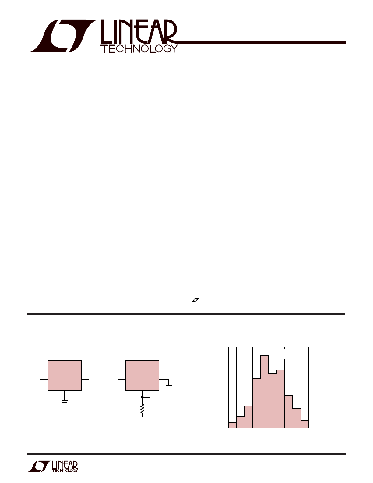
Typical Distribution of Temperature Drift
Basic Positive and Negative Connections
LT1021
IN
V
IN
OUT
GND
V
OUT
R1 =
NC
V
I
LOAD
OUT
LT1021
(7 AND 10 ONLY)
IN
GND
– (V–)
+ 1.5mA
–15V
(V
OUT
–V
OUT
R1
–
)
1021 TA01
24
21
18
15
12
UNITS (%)
9
6
3
– 0
–5
DISTRIBUTION
OF THREE RUNS
–3 –1 1 52–4 –2 0 4
OUTPUT DRIFT (ppm/°C)
3
1021 TA01
1
LT1021
A
W
O
LUTEXI T
S
A
WUW
ARB
U
G
I
(Note 1)
S
Input Voltage .......................................................... 40V
Input/Output Voltage Differential ............................ 35V
Output-to-Ground Voltage (Shunt Mode Current Limit)
LT1021-5............................................................. 10V
LT1021-7............................................................. 10V
LT1021-10........................................................... 16V
Trim Pin-to-Ground Voltage
Positive ............................................... Equal to V
OUT
Negative ........................................................... – 20V
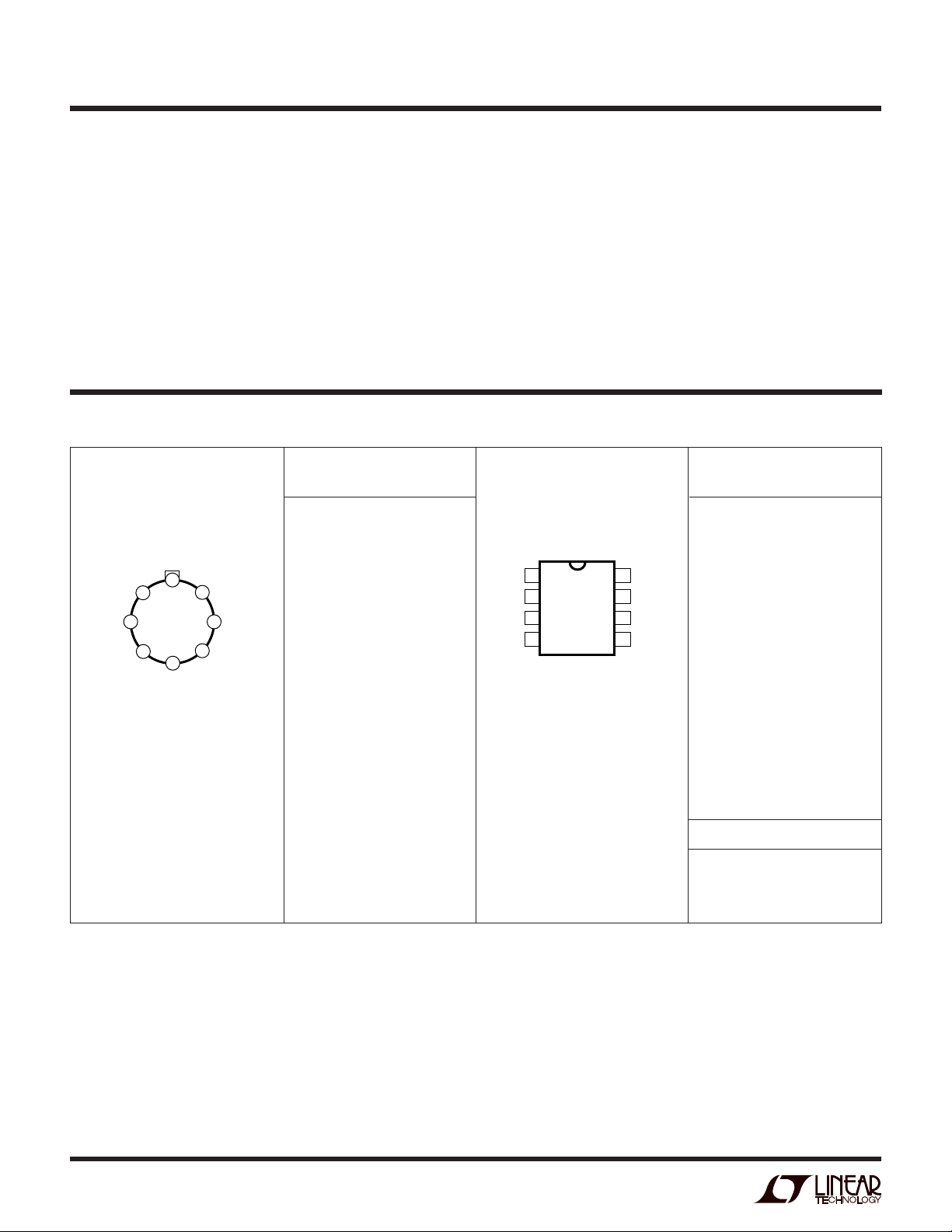
PACKAGE
/
O
RDER I FOR ATIO
WU
U
ORDER PART
NUMBER
LT1021BCH-5
TOP VIEW
NC*
8
1
NC*
2
V
IN
3
NC*
H PACKAGE
8-LEAD TO-5 METAL CAN
CONNECTED INTERNALLY.
*
D0 NOT CONNECT EXTERNAL
CIRCUITRY TO THESE PINS
NO TRIM PIN ON LT1021-7.
**
DO NOT CONNECT EXTERNAL
CIRCUITRY TO PIN 5 ON LT1021-7
T
= 150°C, θJA = 150°C/W,θJC = 45°C/W
JMAX
7
5
4
GND
NC*
6
TRIM
V
OUT
**
LT1021BMH-5
LT1021CCH-5
LT1021CMH-5
LT1021DCH-5
LT1021DMH-5
LT1021BCH-7
LT1021BMH-7
LT1021DCH-7
LT1021DMH-7
LT1021BCH-10
LT1021BMH-10
LT1021CCH-10
LT1021CMH-10
LT1021DCH-10
LT1021DMH-10
Output Short-Circuit Duration
VIN = 35V......................................................... 10 sec
VIN ≤ 20V ................................................... Indefinite
Operating Temperature Range
Commercial ............................................ 0°C to 70°C
Industrial ........................................... –40°C to 85°C
Military ............................................ –55°C to 125°C
Storage Temperature Range ................ –65°C to 150°C
Lead Temperature (Soldering, 10 sec)................ 300°C
ORDER PART
NUMBER
LT1021BCN8-5
TOP VIEW
DNC*
1
V
2
IN
DNC*
3
GND
4
N8 PACKAGE
8-LEAD PDIP
CONNECTED INTERNALLY.
*
D0 NOT CONNECT EXTERNAL
CIRCUITRY TO THESE PINS
NO TRIM PIN ON LT1021-7.
**
DO NOT CONNECT EXTERNAL
CIRCUITRY TO PIN 5 ON LT1021-7
T
= 130°C, θJA = 130°C/W (N)
JMAX
= 130°C, θJA = 150°C/W (S)
T
JMAX
S8 PACKAGE
8-LEAD PLASTIC SO
8
7
6
5
DNC*
DNC*
V
0UT
TRIM**
LT1021CCN8-5
LT1021CIN8-5
LT1021DCN8-5
LT1021DIN8-5
LT1021DCS8-5
LT1021BCN8-7
LT1021DCN8-7
LT1021DCS8-7
LT1021BCN8-10
LT1021CCN8-10
LT1021CIN8-10
LT1021DCN8-10
LT1021DCS8-10
LT1021DIN8-10
S8 PART MARKING
2
021DC5
021DC7
021DC1

LT1021
LECTRICAL C CHARA TERIST
E
range, otherwise specifications are TA = 25°C. VIN = 10V, I
PARAMETER CONDITIONS MIN TYP MAX UNITS
Output Voltage (Note 2) LT1021C-5 4.9975 5.000 5.0025 V
Output Voltage Temperature Coefficient (Note 3) T
Line Regulation (Note 4) 7.2V ≤ VIN ≤ 10V 4 12 ppm/V
Load Regulation (Sourcing Current) 0 ≤ I
Load Regulation (Sinking Current) 0 ≤ I
Supply Current 0.8 1.2 mA
Output Voltage Noise (Note 6) 0.1Hz ≤ f ≤ 10Hz 3.0 µV
Long Term Stability of Output Voltage (Note 7) ∆t = 1000Hrs Noncumulative 15 ppm
Temperature Hysteresis of Output ∆T = ±25°C 10 ppm
ICS
LT1021B-5/LT1021D-5 4.9500 5.000 5.0500 V
≤ TJ ≤ T
MIN
LT1021B-5 ● 2 5 ppm/°C
LT1021C-5/LT1021D-5 ● 3 20 ppm/°C
10V ≤ V
OUT
(Note 4)
OUT
(Note 4)
10Hz ≤ f ≤ 1kHz 2.2 3.5 µV
The ● denotes specifications that apply over the full operating temperature
= 0, unless otherwise noted.
OUT
LT1021-5
MAX
● 20 ppm/V
≤ 40V 2 6 ppm/V
IN
≤ 10mA 10 20 ppm/mA
≤ 10mA 60 100 ppm/mA
● 10 ppm/V
● 35 ppm/mA
● 150 ppm/mA
● 1.5 mA
P-P
RMS
The ● denotes specifications that apply over the full operating temperature range, otherwise specifications are TA = 25°C.
VIN = 12V, I
PARAMETER CONDITIONS MIN TYP MAX UNITS
Output Voltage (Note 2) 6.95 7.00 7.05 V
Output Voltage Temperature Coefficient (Note 3) T
Line Regulation (Note 4) 8.5V ≤ VIN ≤ 12V 1.0 4 ppm/V
Load Regulation (Sourcing Current) 0 ≤ I
Load Regulation (Shunt Mode) 1.2mA ≤ I
Supply Current (Series Mode) 0.75 1.2 mA
Minimum Current (Shunt Mode) VIN is Open 0.7 1.0 mA
Output Voltage Noise (Note 6) 0.1Hz ≤ f ≤ 10Hz 4.0 µV
Long Term Stability of Output Voltage (Note 7) ∆t = 1000Hrs Noncumulative 7 ppm
Temperature Hysteresis of Output ∆T = ±25°C 3 ppm
= 0, unless otherwise noted.
OUT
LT1021-7
≤ TJ ≤ T
MIN
LT1021B-7 ● 2 5 ppm/°C
LT1021D-7
12V ≤ V
(Note 4)
(Notes 4, 5)
10Hz ≤ f ≤ 1kHz 2.5 4.0 µV
MAX
● 3 20 ppm/°C
● 2.0 8 ppm/V
≤ 40V 0.5 2 ppm/V
IN
≤ 10mA 12 25 ppm/mA
OUT
≤ 10mA 50 100 ppm/mA
SHUNT
● 1.0 4 ppm/V
● 40 ppm/mA
● 150 ppm/mA
● 1.5 mA
● 1.2 mA
P-P
RMS
3

LT1021
LECTRICAL C CHARA TERIST
E
range, otherwise specifications are TA = 25°C. VIN = 15V, I
PARAMETER CONDITIONS MIN TYP MAX UNITS
Output Voltage (Note 2) LT1021C-10 9.995 10.00 10.005 V
Output Voltage Temperature Coefficient (Note 3) T
Line Regulation (Note 4) 11.5V ≤ VIN ≤ 14.5V 1.0 4 ppm/V
Load Regulation (Sourcing Current) 0 ≤ I
Load Regulation (Shunt Mode) 1.7mA ≤ I
Supply Current (Series Mode) 1.2 1.7 mA
Minimum Current (Shunt Mode) VIN is Open 1.1 1.5 mA
Output Voltage Noise (Note 6) 0.1Hz ≤ f ≤ 10Hz 6.0 µV
Long Term Stability of Output Voltage (Note 7) ∆t = 1000Hrs Noncumulative 15 ppm
Temperature Hysteresis of Output ∆T = ±25°C 5 ppm
ICS
LT1021B-10/LT1021D-10 9.950 10.00 10.050 V
≤ TJ ≤ T
MIN
LT1021B-10 ● 2 5 ppm/°C
LT1021C-10/LT1021D-10 ● 5 20 ppm/°C
14.5V ≤ V
OUT
(Note 4)
(Notes 4, 5)
10Hz ≤ f ≤ 1kHz 3.5 6 µV
The ● denotes specifications that apply over the full operating temperature
= 0, unless otherwise noted.
OUT
LT1021-10
MAX
● 6 ppm/V
≤ 40V 0.5 2 ppm/V
IN
≤ 10mA 12 25 ppm/mA
≤ 10mA 50 100 ppm/mA
SHUNT
● 4 ppm/V
● 40 ppm/mA
● 150 ppm/mA
● 2.0 mA
● 1.7 mA
P-P
RMS
Note 1: Absolute Maximum Ratings are those values beyond which the life
of a device may be impaired.
Note 2: Output voltage is measured immediately after turn-on. Changes
due to chip warm-up are typically less than 0.005%.
Note 3: Temperature coefficient is measured by dividing the change in
output voltage over the temperature range by the change in temperature.
Separate tests are done for hot and cold; T
Incremental slope is also measured at 25°C.
Note 4: Line and load regulation are measured on a pulse basis. Output
changes due to die temperature change must be taken into account
separately. Package thermal resistance is 150°C/W for TO-5 (H), 130°C/W
for N and 150°C/W for the SO-8.
to 25°C and 25°C to T
MIN
MAX
.
Note 5: Shunt mode regulation is measured with the input open. With the
input connected, shunt mode current can be reduced to 0mA. Load
regulation will remain the same.
Note 6: RMS noise is measured with a 2-pole highpass filter at 10Hz and a
2-pole lowpass filter at 1kHz. The resulting output is full-wave rectified and
then integrated for a fixed period, making the final reading an average as
opposed to RMS. Correction factors are used to convert from average to
RMS and correct for the non-ideal bandpass of the filters.
Peak-to-peak noise is measured with a single highpass filter at 0.1Hz and a
2-pole lowpass filter at 10Hz. The unit is enclosed in a still-air environment
to eliminate thermocouple effects on the leads. Test time is 10 seconds.
Note 7: Consult factory for units with long term stability data.
4

LPER
OUTPUT CURRENT (mA)
0
INPUT/OUTPUT VOLTAGE (V)
1.2
1.6
16
1021 G03
0.8
0.4
0
4
8
12
20
1.0
1.4
0.6
0.2
14
2
6
10
18
TJ = 125 °C
TJ = –55 °C
TJ = 25 °C
FREQUENCY (Hz)
100
NOISE VOLTAGE (nV/√Hz)
200
250
350
400
10 1k 10k
LT1021 G06
0
100
300
150
50
LT1021-10
LT1021-5
LT1021-7
Ripple Rejection
115
f = 150Hz
110
105
100
REJECTION (dB)
95
90
85
0
13
12
11
10
9
8
7
6
OUTPUT VOLTAGE (V)
5
4
3
10 20
515
INPUT VOLTAGE (V)
Start-Up (Series Mode)
VIN = 0V TO 12V
04
2
F
LT1021-10
LT1021-7
LT1021-5
6
TIME (µs)
R
O
LT1021-7
LT1021-10
LT1021-5
25
8
LT1021
UW
ATYPICA
30
10
35
LT1021 G01
12
LT1021 G04
40
14
CCHARA TERIST
E
C
Ripple Rejection
130
VIN = 15V
= 0
C
OUT
120
110
100
90
80
REJECTION (dB)
70
60
50
10
Start-Up (Shunt Mode)
LT1021-7, LT1021-10
11
10
9
8
7
OUTPUT VOLTAGE (V)
6
5
02
ICS
LT1021-7
LT1021-10
LT1021-5
100 1k 10k
FREQUENCY (Hz)
LT1021-10
+ 2V
V
OUT
0V
NC
LT1021-7
61012
48
TIME (µs)
LT1021 G02
1k
V
OUT
OUT
IN
GND
LT1021 G05
Minimum Input/Output Differential
LT1021-7, LT1021-10
Output Voltage Noise Spectrum
Output Voltage Noise
16
C
= 0
OUT
FILTER = 1 POLE
14
= 0.1Hz
f
LOW
12
10
8
6
RMS NOISE (µV)
4
2
0
10
LT1021-10
100 1k 10k
BANDWIDTH (Hz)
LT1021-7
LT1021-5
LT1021 G07
Output Voltage Temperature Drift
LT1021-5
5.006
5.004
5.002
5.000
4.998
OUTPUT VOLTAGE (V)
4.996
4.994
–50
0
–25
TEMPERATURE (°C)
50
25
Load Regulation LT1021-5
5
VIN = 8V
4
3
2
1
0
–1
–2
OUTPUT CHANGE (mV)
–3
–4
100
LT1021 G08
125
75
–5
–6–8 –4 0 4 8
–10
–2
SOURCING SINKING
OUTPUT CURRENT (mA)
2
6
10
LT1021 G09
5
 Loading...