

Linear Technology LT1019 Datasheet
FEATURES
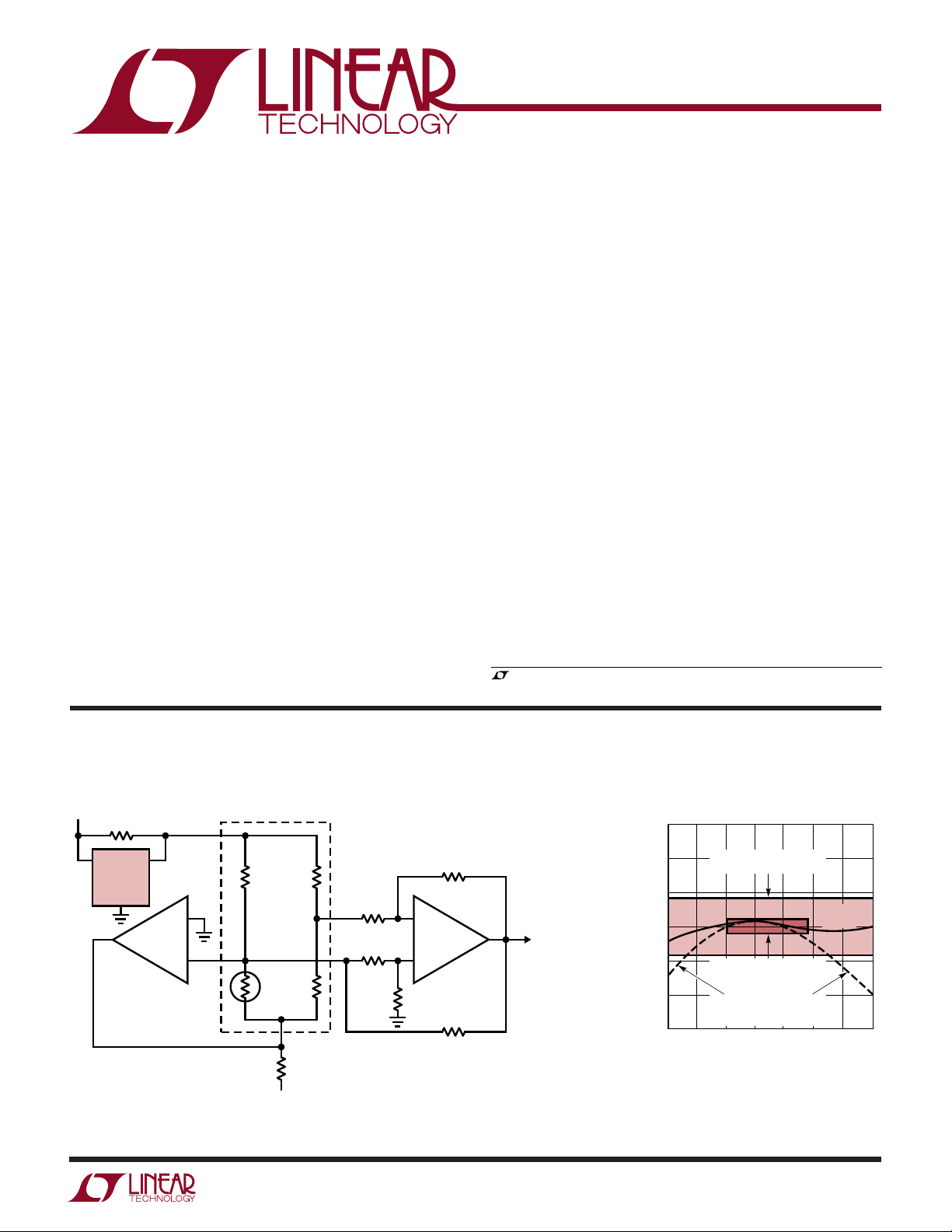
TEMPERATURE (˚C)
–50
OUTPUT VOLTAGE (NORMALIZED) (V)
1.001
1.002
1.003
25 75
1019 TA02
1.000
0.999
–25 0
50 100 125
0.998
0.997
5ppm/°C
0°C TO 70°C “BOX”
LT1019
CURVE
UNCOMPENSATED
“STANDARD” BANDGAP
DRIFT CURVE
10ppm/°C
FULL TEMP RANGE “BOX”
LT1019
Precision Reference
U
DESCRIPTIO
■
Tight Initial Output Voltage: <0.05%
■
Ultralow Drift: 3ppm/°C Typical
■
Series or Shunt Operation
■
Curvature Corrected
■
Ultrahigh Line Rejection: ≈0.5ppm/V
■
Low Output Impedance: ≈0.02Ω
■
Plug-In Replacement for Present References
■
Available at 2.5V, 4.5V, 5V, and 10V
■
100% Noise Tested
■
Temperature Output
■
Industrial Temperature Range in SO-8
U
APPLICATIO S
■
Negative Shunt References
■
A/D and D/A Converters
■
Precision Regulators
■
Constant Current Sources
■
V/F Converters
■
Bridge Excitation
The LT®1019 is a third generation bandgap voltage reference utilizing thin film technology and a greatly improved
curvature correction technique. Wafer level trimming of
both reference and output voltage combines to produce
units with high yields to very low TC and tight initial
tolerance of output voltage.
The LT1019 can both sink and source up to 10mA and can
be used in either the series or shunt mode. This allows the
reference to be used for both positive and negative output
voltages without external components. Minimum input/
output voltage is less than 1V in the series mode, providing
improved tolerance of low line conditions.
The LT1019 is available in four voltages: 2.5V, 4.5V, 5V
and 10V. It is a direct replacement for most bandgap
references presently available including AD580, AD581,
REF-01, REF-02, MC1400, MC1404 and LM168.
, LTC and LT are registered trademarks of Linear Technology Corporation.
TYPICAL APPLICATION
15V
357Ω*
0.5W
IN
LT1019-5
GND
5V
OUT
†
A1
LT1637
Ultralinear Strain Guage
350Ω
BRIDGE
+
–
ACTIVE
ELEMENT
–15V
–5V
357Ω*
0.5W
U
R3
2M
R2
20k
R4
20k
*
REDUCES REFERENCE AND AMPLIFIER
LOADING TO ≈0.
**
IF R6 = R3, BRIDGE IS NOT LOADED BY R2 AND R4.
†
A1 V
ACTS AS A DIFFERENTIAL AMPLIFIER.
–
A2
LT1001
+
R5
2M
R6**
2M
LT1019 • TA01
AND DRIFT ARE NOT CRITICAL BECAUSE A2
OS
Output Voltage Drift
GAIN = 100
1
LT1019
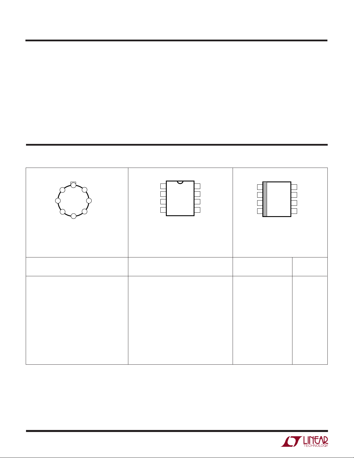
TOP VIEW
S8 PACKAGE
8-LEAD PLASTIC SO
1
2
3
4
8
7
6
5
DNC*
INPUT
TEMP
GND
DNC*
DNC*
OUTPUT
TRIM
*INTERNALLY CONNECTED. DO NOT
CONNECT EXTERNALLY.
A
W
O
LUTEXI TIS
S
A
WUW
U
ARB
G
(Note 1)
Input Voltage .......................................................... 40V
Output Voltage (Note 2)
LT1019-5, LT1019-10 ........................................ 16V
LT1019-2.5, LT1019-4.5 ...................................... 7V
Output Short-Circuit Duration (Note 2)
VIN < 20V.................................................... Indefinite
20V ≤ VIN ≤ 35V ............................................. 10 sec
WU
/
PACKAGE
DNC*
INPUT
TEMP
8-LEAD TO-5 METAL CAN
*INTERNALLY CONNECTED. DO NOT
CONNECT EXTERNALLY
T
= 150°C, θ
JMAX
O
RDER I FOR ATIO
TOP VIEW
DNC*
8
1
2
3
4
GND (CASE)
H PACKAGE
= 150°C/ W, θJC = 45°C/W
JA
DNC*
7
DNC*
6
OUTPUT
5
TRIM
1
INPUT
2
TEMP
3
GND
4
*INTERNALLY CONNECTED. DO NOT
CONNECT EXTERNALLY.
T
= 100°C, θ
JMAX
Specified Temperature Range
Commercial .............................................0°C to 70°C
Industrial ............................................ –40°C to 85°C
Military ............................................. –55°C to 125°C
Trim Pin Voltage................................................... ±30V
Temp Pin Voltage ..................................................... 5V
Storage Temperature Range (Note 11) –65°C to 150°C
Lead Temperature (Soldering, 10 sec)................. 300°C
U
TOP VIEW
DNC*
8
DNC*
7
OUTPUT
6
TRIM
5
N8 PACKAGE
8-LEAD PDIP
T
= 130°C/ W
JA
JMAX
= 100°C, θ
= 130°C/ W
JA
LT1019ACH-2.5
LT1019ACH-4.5
LT1019ACH-5
LT1019ACH-10
LT1019AMH-2.5
LT1019AMH-4.5
LT1019AMH-5
LT1019AMH-10
ORDER PART
NUMBER
LT1019CH-2.5
LT1019CH-4.5
LT1019CH-5
LT1019CH-10
LT1019MH-2.5
LT1019MH-4.5
LT1019MH-5
LT1019MH-10
ORDER PART
NUMBER
LT1019ACN8-2.5
LT1019ACN8-4.5
LT1019ACN8-5
LT1019ACN8-10
LT1019CN8-2.5
LT1019CN8-4.5
LT1019CN8-5
LT1019CN8-10
LT1019IN8-2.5
LT1019IN8-4.5
LT1019IN8-5
LT1019IN8-10
ORDER PART
NUMBER
LT1019ACS8-2.5
LT1019ACS8-5
LT1019AIS8-2.5
LT1019AIS8-5
LT1019CS8-2.5
LT1019CS8-4.5
LT1019CS8-5
LT1019CS8-10
LT1019IS8-2.5
LT1019IS8-5
S8 PART
MARKING
19A25
19A05
19AI2
19AI5
1925
1945
1905
1910
19I25
19I05
2
U
AVAILABLE OPTIO S
LT1019
OUTPUT TEMPERATURE
VOLTAGE TEMPERATURE ACCURACY COEFFICIENT TO-5 SO-8 PDIP-8
(V) (
2.5 0 to 70 0.05 5 LT1019ACH-2.5 LT1019ACS8-2.5 LT1019ACN8-2.5
4.5 0 to 70 0.05 5 LT1019ACH-4.5 LT1019ACN8-4.5
5 0 to 70 0.05 5 LT1019ACH-5 LT1019ACS8-5 LT1019ACN8-5
10 0 to 70 0.05 5 LT1019ACH-10 LT1019ACN8-10
°
C) (%) (ppm/°C) H8 S8 N8
0.2 20 LT1019CH-2.5 LT1019CS8-2.5 LT1019CN8-2.5
–40 to 85 0.05 10 LT1019AIS8-2.5
0.2 20 LT1019IS8-2.5 LT1019IN8-2.5
–55 to 125 0.05 10 LT1019AMH-2.5
0.2 25 LT1019MH-2.5
0.2 20 LT1019CH-4.5 LT1019CS8-4.5 LT1019CN8-4.5
–40 to 85 0.2 20 LT1019IN8-4.5
–55 to 125 0.05 10 LT1019AMH-4.5
0.2 25 LT1019MH-4.5
0.2 20 LT1019CH-5 LT1019CS8-5 LT1019CN8-5
–40 to 85 0.05 10 LT1019AIS8-5
0.2 20 LT1019IS8-5 LT1019IN8-5
–55 to 125 0.05 10 LT1019AMH-5
0.2 25 LT1019MH-5
0.2 20 LT1019CH-10 LT1019CS8-10 LT1019CN8-10
–40 to 85 0.2 20 LT1019IN8-10
–55 to 125 0.05 10 LT1019AMH-10
0.2 25 LT1019MH-10
PACKAGE TYPE
LECTRICAL C CHARA TERIST
E
The ● denotes specifications which apply over the full operating temperature range, otherwise specifications are TA = 25°C.
VIN = 15V, I
SYMBOL PARAMETER CONDITIONS MIN TYP MAX MIN TYP MAX UNITS
TC Output Voltage LT1019C (0°C to 70°C) ● 3 5 5 20 ppm/°C
∆V
OUT
∆V
IN
RR Ripple Rejection 50Hz ≤ f ≤ 400Hz 90 110 90 110 dB
= 0 unless otherwise noted.
OUT
Output Voltage Tolerance 0.02 0.05 0.02 0.2 %
Temperature Coefficient LT1019I (–40°C to 85°C)
(Note 3) LT1019M (–55°C to 125°C)
Line Regulation (Note 4) (V
OUT
ICS
LT1019A LT1019
● 3 10 5 20 ppm/°C
● 5 10 8 25 ppm/°C
+ 1.5V) ≤ VIN ≤ 40V 0.5 3 0.5 3 ppm/V
● 1.0 5 1.0 5 ppm/V
● 84 84 dB
3
LT1019
LECTRICAL C CHARA TERIST
E
The ● denotes specifications which apply over the full operating temperature range, otherwise specifications are TA = 25°C.
VIN = 15V, I
SYMBOL PARAMETER CONDITIONS MIN TYP MAX MIN TYP MAX UNITS
∆V
OUT
∆I
OUT
I
Q
I
SC
e
n
= 0 unless otherwise noted.
OUT
Load Regulation Series 0 ≤ I
Mode (Notes 4, 5) ● 0.08 0.08 mV/mA (Ω)
Load Regulation, 1mA ≤ I
Shunt Mode 2.5V, 4.5V, 5V
Thermal Regulation (Note 7) ∆P = 200mW, t = 50ms 0.1 0.5 0.1 0.5 ppm/mW
Quiescent Current 0.65 1.0 0.65 1.2 mA
Series Mode
Minimum Shunt Current (Note 8) ● 0.5 0.8 0.5 0.8 mA
Minimum Input/Output I
Voltage Differential I
Trim Range LT1019-2.5 ±3.5 ±6 ±3.5 ±6%
Short-Circuit Current 2V ≤ VIN ≤ 35V 15 25 50 15 25 50 mA
Output Connected to GND
Output Voltage Noise 10Hz ≤ f ≤ 1kHz 2.5 4 2.5 4 ppm (RMS)
(Note 10) 0.1Hz ≤ f ≤ 10Hz 2.5 2.5 ppm (P-P)
OUT
10V
≤ 1mA ● 0.9 1.1 0.9 1.1 V
OUT
= 10mA ● 1.3 1.3 V
OUT
LT1019-5 ±3.5 5, –13 ±3.5 5, –13 %
LT1019-10 ±3.5 5, –27 ±3.5 5, –27 %
ICS
LTC1019A LTC1019
≤ 10mA (Note 5) 0.02 0.05 0.02 0.05 mV/mA (Ω)
≤ 10mA (Notes 5, 6)
SHUNT
● 0.1 0.4 0.1 0.4 mV/mA (Ω)
● 0.8 0.8 mV/mA (Ω)
● 1.3 1.5 mA
● 10 10 mA
Note 1: Absolute Maximum Ratings are those values beyond which the life
of a device may be impaired.
Note 2: These are high power conditions and are therefore guaranteed
only at temperatures equal to or below 70°C. Input is either floating, tied to
output or held higher than output.
Note 3: Output voltage drift is measured using the box method. Output
voltage is recorded at T
readings is subtracted from the highest and the resultant difference is
divided by (T
Note 4: Line regulation and load regulation are measured on a pulse basis
with low duty cycle. Effects due to die heating must be taken into account
separately. See thermal regulation and application section.
Note 5: Load regulation is measured at a point 1/8" below the base of the
package with Kelvin contacts.
Note 6: Shunt regulation is measured with the input floating. This
parameter is also guaranteed with the input connected (V
0mA ≤ I
– T
MAX
≤ 10mA. Shunt and sink current flow into the output.
SINK
MIN
MIN
).
, 25°C and T
. The lowest of these three
MAX
– V
IN
OUT
) > 1V,
Note 7: Thermal regulation is caused by die temperature gradients created
by load current or input voltage changes. This effect must be added to
normal line or load regulation.
Note 8: Minimum shunt current is measured with shunt voltage held
20mV below the value measured at 1mA shunt current.
Note 9: Minimum input/output voltage is measured by holding input
voltage 0.5V above the nominal output voltage, while measuring
– V
OUT
.
V
IN
Note 10: RMS noise is measured with a single pole highpass filter at 10Hz
and a 2-pole lowpass filter at 1kHz. The resulting output is full-wave
rectified and then integrated for a fixed period, making the final reading an
average as opposed to RMS. A correction factor of 1.1 is used to convert
from average to RMS, and a second correction of 0.88 is used to correct
the nonideal bandpass of the filters.
Note 11: If the part is stored outside of the specified temperature range,
the output may shift due to hysteresis.
4
 Loading...