

FEATURES
LT1016
UltraFast Precision
10ns Comparator
U
DESCRIPTIO
■
UltraFastTM (10ns typ)
■
Operates Off Single 5V Supply or ±5V
■
Complementary Output to TTL
■
Low Offset Voltage
■
No Minimum Input Slew Rate Requirement
■
No Power Supply Current Spiking
■
Output Latch Capability
U
APPLICATIO S
■
High Speed A/D Converters
■
High Speed Sampling Circuits
■
Line Receivers
■
Extended Range V-to-F Converters
■
Fast Pulse Height/Width Discriminators
■
Zero-Crossing Detectors
■
Current Sense for Switching Regulators
■
High Speed Triggers
■
Crystal Oscillators
, LTC and LT are registered trademarks of Linear Technology Corporation.
UltraFast is a trademark of Linear Technology Corporation.
The LT®1016 is an UltraFast 10ns comparator that interfaces directly to TTL/CMOS logic while operating off either
±5V or single 5V supplies. Tight offset voltage specifications and high gain allow the LT1016 to be used in
precision applications. Matched complementary outputs
further extend the versatility of this comparator.
A unique output stage provides active drive in both directions for maximum speed into TTL/CMOS logic or passive
loads, yet does not exhibit the large current spikes found
in conventional output stages. This allows the LT1016 to
remain stable with the outputs in the active region which,
greatly reduces the problem of output “glitching” when the
input signal is slow moving or is␣ low level.
The LT1016 has a LATCH pin which will retain input data
at the outputs, when held high. Quiescent negative power
supply current is only 3mA. This allows the negative
supply pin to be driven from virtually any supply voltage
with a simple resistive␣ divider. Device performance is not
affected by variations in negative supply voltage.
Linear Technology offers a wide range of comparators in
addition to the LT1016 that address different applications.
See the Related Parts section on the back page of the data
sheet.
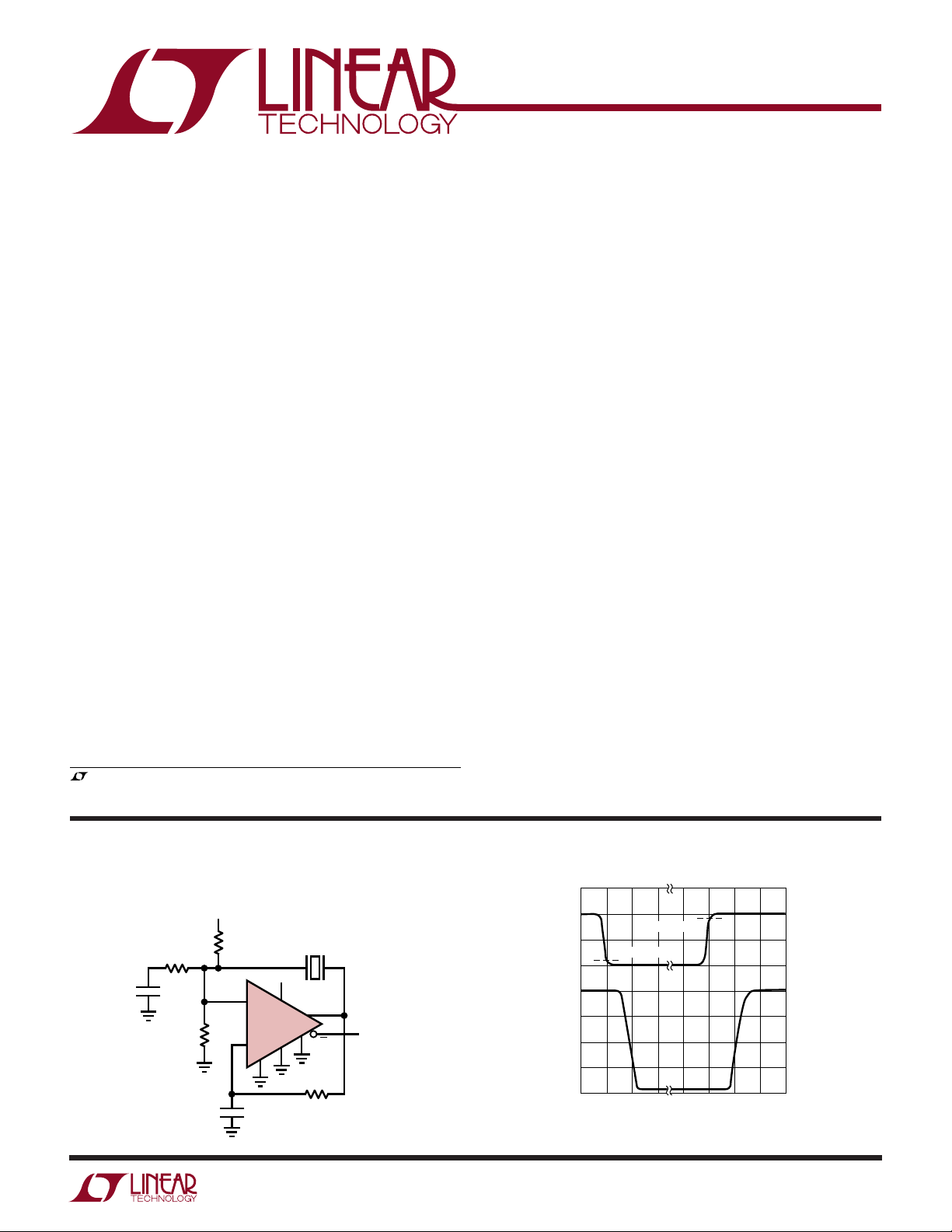
TYPICAL APPLICATION
10MHz to 25MHz Crystal Oscillator
5V
22Ω
2k
820pF
2k
10MHz TO 25MHz
5V
+
LT1016
–
–
V
200pF
(AT CUT)
+
V
LATCH
GND
U
Response Time
THRESHOLD
0
THRESHOLD
20
TIME (ns)
0
20
1016 TA2b
V
V
OUT
1V/DIV
IN
100mV STEP
5mV OVERDRIVE
Q
OUTPUT
Q
2k
1016 TA1a
1
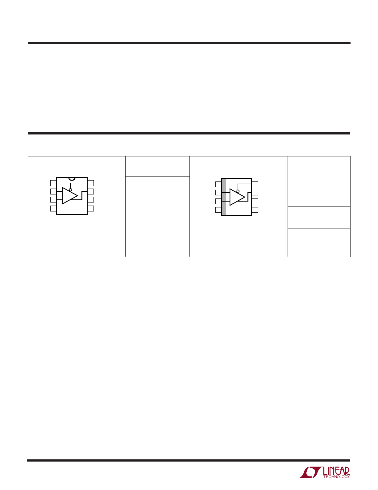
LT1016
TOP VIEW
Q OUT
Q OUT
GND
LATCH
ENABLE
V
+
+IN
–IN
V
–
S8 PACKAGE
8-LEAD PLASTIC SO
1
2
3
4
8
7
6
5
+
–
WW
W
ABSOLUTE AXI U RATI GS
U
(Note 1)
Positive Supply Voltage (Note 5) ............................... 7V
Negative Supply Voltage ............................................ 7V
Differential Input Voltage (Note 7) ........................... ±5V
+IN, –IN and LATCH ENABLE Current (Note 7) .. ±10mA
Output Current (Continuous) (Note 7) ................ ±20mA
UUW
PACKAGE/ORDER I FOR ATIO
ORDER PART
TOP VIEW
+
V
1
+IN
–IN
V
+
2
–
3
–
4
N8 PACKAGE
8-LEAD PDIP
T
= 100°C, θJA = 130°C/W (N8)
JMAX
8
7
6
5
Q OUT
Q OUT
GND
LATCH
ENABLE
NUMBER
LT1016CN8
LT1016IN8
Operating Temperature Range
LT1016I ...............................................–40°C to 85°C
LT1016C..................................................0°C to 70°C
Storage Temperature Range ................. –65°C to 150°C
Lead Temperature (Soldering, 10 sec).................. 300°C
ORDER PART
NUMBER
LT1016CS8
LT1016IS8
S8 PART
MARKING
T
= 110°C, θJA = 120°C/W
JMAX
1016
1016I
Consult LTC marketing for parts specified with wider operating temperature ranges.
2
LT1016
ELECTRICAL CHARACTERISTICS
temperature range, otherwise specifications are at TA = 25°C. V+ = 5V, V– = 5V, V
The ● denotes the specifications which apply over the full operating
(Q) = 1.4V, V
OUT
= 0V, unless otherwise noted.
LATCH
LT1016C/I
SYMBOL PARAMETER CONDITIONS MIN TYP MAX UNITS
V
∆V
OS
OS
Input Offset Voltage RS ≤ 100Ω (Note 2) 1.0 ±3mV
● 3.5 mV
Input Offset Voltage Drift ● 4 µV/°C
∆T
I
OS
I
B
Input Offset Current (Note 2) 0.3 1.0 µA
● 0.3 1.3 µA
Input Bias Current (Note 3) 5 10 µA
● 13 µA
Input Voltage Range (Note 6) ● –3.75 3.5 V
Single 5V Supply
● 1.25 3.5 V
CMRR Common Mode Rejection –3.75V ≤ VCM ≤ 3.5V ● 80 96 dB
PSRR Supply Voltage Rejection Positive Supply 4.6V ≤ V+ ≤ 5.4V ● 60 75 dB
LT1016C
Positive Supply 4.6V ≤ V+ ≤ 5.4V ● 54 75 dB
LT1016I
Negative Supply 2V ≤ V– ≤ 7V ● 80 100 dB
A
V
V
OH
V
OL
+
I
–
I
V
IH
V
IL
I
IL
t
PD
Small-Signal Voltage Gain 1V ≤ V
Output High Voltage V+ ≥ 4.6V I
Output Low Voltage I
≤ 2V 1400 3000 V/V
OUT
=1mA ● 2.7 3.4 V
OUT
I
= 10mA ● 2.4 3.0 V
OUT
= 4mA ● 0.3 0.5 V
SINK
= 10mA 0.4 V
I
SINK
Positive Supply Current ● 25 35 mA
Negative Supply Current ● 35 mA
LATCH Pin Hi Input Voltage ● 2.0 V
LATCH Pin Lo Input Voltage ● 0.8 V
LATCH Pin Current V
= 0V ● 500 µA
LATCH
Propagation Delay (Note 4) ∆VIN = 100mV, OD = 5mV 10 14 ns
● 16 ns
∆VIN = 100mV, OD = 20mV 9 12 ns
● 15 ns
∆t
PD
Differential Propagation (Note 4) ∆VIN = 100mV, 3 ns
Delay OD = 5mV
Latch Setup Time 2ns
Note 1: Absolute Maximum Ratings are those values beyond which the life
of a device may be impaired.
Note 2: Input offset voltage is defined as the average of the two voltages
measured by forcing first one output, then the other to 1.4V. Input offset
current is defined in the same way.
Note 3: Input bias current (IB) is defined as the average of the two input
currents.
Note 4: t
and ∆tPD cannot be measured in automatic handling
PD
equipment with low values of overdrive. The LT1016 is sample tested with
a 1V step and 500mV overdrive. Correlation tests have shown that tPD and
∆tPD limits shown can be guaranteed with this test if additional DC tests
are performed to guarantee that all internal bias conditions are correct. For
low overdrive conditions VOS is added to overdrive. Differential
= t
propogation delay is defined as: ∆t
PD
PDLH
– t
PDHL
Note 5: Electrical specifications apply only up to 5.4V.
Note 6: Input voltage range is guaranteed in part by CMRR testing and in
part by design and characterization. See text for discussion of input
voltage range for supplies other than ±5V or 5V.
Note 7: This parameter is guaranteed to meet specified performance
through design and characterization. It has not been tested.
3
LT1016
UW
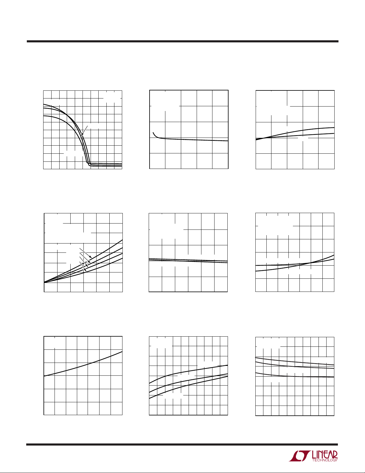
TYPICAL PERFOR A CE CHARACTERISTICS
Gain Characteristics
5.0
4.5
TJ = 125°C
4.0
3.5
3.0
2.5
2.0
1.5
OUTPUT VOLTAGE (V)
1.0
0.5
0
–2.5 –1.5
TJ = –55°C
–0.5
DIFFERENTIAL INPUT VOLTAGE (mV)
Propagation Delay vs Source
Resistance
80
VS = ±5V
= 25°C
T
J
70
OVERDRIVE = 20mV
EQUIVALENT INPUT
60
CAPACITANCE IS ≈ 3.5pF
= 10pF
C
LOAD
50
STEP SIZE = 800mV
40
TIME (ns)
30
20
10
0
0 500
400mV
200mV
100mV
1k 2k1.5k
SOURCE RESISTANCE (Ω)
VS = ±5V
= 0
I
OUT
TJ = 25°C
0.5 1.5 2.5
1016 G01
2.5k
1016 G04
Propagation Delay vs Input
Overdrive
25
VS = ±5V
= 25°C
T
J
= 100mV
V
STEP
20
15
TIME (ns)
10
= 10pF
C
LOAD
5
0
10
0
OVERDRIVE (mV)
30
40
20
50
1016 G02
Propagation Delay vs Supply
Voltage
25
V– = –5V
= 25°C
T
J
= 100mV
V
STEP
20
OVERDRIVE = 5mV
= 10pF
C
LOAD
15
TIME (ns)
10
RISING EDGE t
5
0
4.4
3k
4.6
POSITIVE SUPPLY VOLTAGE (V)
FALLING EDGE t
PDLH
4.8 5.0 5.2
PDHL
5.4 5.6
1016 G05
Propagation Delay vs Load
Capacitance
25
VS = ±5V
= 25°C
T
J
= 0
I
OUT
20
15
TIME (ns)
10
= 100mV
V
STEP
OVERDRIVE = 5mV
t
PDHL
5
0
10
0
OUTPUT LOAD CAPACITANCE (pF)
20
Propagation Delay vs
Temperature
30
VS = ±5V
OVERDRIVE = 5mV
25
STEP SIZE = 100mV
C
= 10pF
LOAD
20
15
TIME (ns)
FALLING OUTPUT t
10
5
0
–50
–25 0
JUNCTION TEMPERATURE (°C)
PDHL
RISING OUTPUT t
25 75
t
PDLH
30
40
50
1016 G03
PDLH
50 100 125
1016 G06
Latch Set-Up Time vs
Temperature
6
VS = ±5V
= 0V
I
OUT
4
2
0
TIME (ns)
–2
–4
–6
–50
–25 0
JUNCTION TEMPERATURE (°C)
4
50 100 125
25 75
1016 G07
Output Low Voltage (VOL) vs
Output Sink Current
0.8
VS = ±5V
= 30mV
V
IN
0.7
0.6
0.5
0.4
0.3
OUTPUT VOLTAGE (V)
0.2
0.1
0
0
TJ = 25°C
TJ = 125°C
42 6 10 14 18
8
OUTPUT SINK CURRENT (mA)
TJ = –55°C
12
Output High Voltage (VOH) vs
Output Source Current
5.0
VS = ±5V
V
= –30mV
IN
4.5
4.0
3.5
3.0
2.5
OUTPUT VOLTAGE (V)
2.0
1.5
16
20
1016 G08
1.0
TJ = –55°C
0
OUTPUT SOURCE CURRENT (mA)
TJ = 25°C
42 6 10 14 18
8
12
TJ = 125°C
16
1016 G09
20

UW
JUNCTION TEMPERATURE (°C)
–50
INPUT VOLTAGE (V)
2
1
0
–1
–2
–3
–4
25 75
1016 G15
–25 0
50 100 125
VS = ±5V*
VS = SINGLE 5V SUPPLY
*SEE APPLICATION INFORMATION
FOR COMMON MODE LIMIT WITH
VARYING SUPPLY VOLTAGE.
TYPICAL PERFOR A CE CHARACTERISTICS
LT1016
Negative Supply Current vs
Temperature
6
VS = ±5V
I
= 0
OUT
5
4
3
CURRENT (mA)
2
1
0
–50
–25 0
25 75
JUNCTION TEMPERATURE (°C)
Common Mode Rejection vs
Frequency
120
110
100
90
80
70
REJECTION RATIO (dB)
60
50
40
10k
100k 1M 10M
FREQUENCY (Hz)
50 100 125
1016 G10
VS = ±5V
= 2V
V
IN
P-P
TJ = 25°C
1016 G13
Positive Supply Current vs
Positive Supply Voltage
50
V– = 0V
45
V
= 60mV
IN
= 0
I
OUT
40
35
30
25
20
CURRENT (mA)
15
TJ = 125°C
10
5
0
0
13
2
SUPPLY VOLTAGE (V)
TJ = 25°C
TJ = –55°C
4
5
Positive Common Mode Limit vs
Temperature
6
VS = ±5V*
5
4
3
2
INPUT VOLTAGE (V)
*SEE APPLICATION INFORMATION
1
FOR COMMON MODE LIMIT WITH
VARYING SUPPLY VOLTAGE.
0
–50
–25 0
JUNCTION TEMPERATURE (°C)
50 100 125
25 75
Positive Supply Current vs
Switching Frequency
40
35
30
25
20
15
CURRENT (mA)
10
VS = ±5V
5
= ±50mV
V
IN
I
= 0
OUT
0
7
6
8
1016 G11
1
SWITCHING FREQUENCY (MHz)
10 100
= 125°C
T
J
T
= 25°C
J
TJ = –55°C
1016 G12
Negative Common Mode Limit vs
Temperature
1016 G14
2.6
2.2
1.8
1.4
VOLTAGE (V)
1.0
0.6
0.2
LATCH Pin Threshold vs
Temperature
VS = ±5V
OUTPUT LATCHED
OUTPUT UNAFFECTED
50 100 125
–50
–25 0
25 75
JUNCTION TEMPERATURE (°C)
1016 G16
LATCH Pin Current* vs
Temperature
300
VS = ±5V
= 0V
V
LATCH
250
200
150
CURRENT (µA)
100
50
*CURRENT COMES OUT OF
LATCH PIN BELOW THRESHOLD
0
–50
–25 0
JUNCTION TEMPERATURE (°C)
50 100 125
25 75
1016 G17
5

LT1016
WUUU
APPLICATIO S I FOR ATIO
Common Mode Considerations
The LT1016 is specified for a common mode range of
–3.75V to 3.5V with supply voltages of ±5V. A more
general consideration is that the common mode range is
1.25V above the negative supply and 1.5V below the
positive supply, independent of the actual supply voltage.
The criteria for common mode limit is that the output still
responds correctly to a small differential input signal.
Either input may be outside the common mode limit (up to
the supply voltage) as long as the remaining input is within
the specified limit, and the output will still respond correctly. There is one consideration, however, for inputs that
exceed the positive common mode limit. Propagation
delay will be increased by up to 10ns if the signal input is
more positive than the upper common mode limit and then
switches back to within the common mode range. This
effect is not seen for signals more negative than the lower
common mode limit.
Input Impedance and Bias Current
Input bias current is measured with the output held at
1.4V. As with any simple NPN differential input stage, the
LT1016 bias current will go to zero on an input that is low
and double on an input that is high. If both inputs are less
than 0.8V above V–, both input bias currents will go to
zero. If either input exceeds the positive common mode
limit, input bias current will increase rapidly, approaching
several milliamperes at VIN = V+.
Differential input resistance at zero differential input
voltage is about 10kΩ, rapidly increasing as larger DC
differential input signals are applied. Common mode input
resistance is about 4MΩ with zero differential input
voltage. With large differential input signals, the high input
will have an input resistance of about 2MΩ and the low
input greater than 20MΩ.
Input capacitance is typically 3.5pF. This is measured by
inserting a 1k resistor in series with the input and measuring the resultant change in propagation delay.
LATCH Pin Dynamics
The LATCH pin is intended to retain input data (output
latched) when the LATCH pin goes high. This pin will float
to a high state when disconnected, so a flowthrough
condition requires that the LATCH pin be grounded. To
guarantee data retention, the input signal must be valid at
least 5ns before the latch goes high (setup time) and must
remain valid at least 3ns after the latch goes high (hold
time). When the latch goes low, new data will appear at the
output in approximately 8ns to 10ns. The LATCH pin is
designed to be driven with TTL or CMOS gates. It has no
built-in hysteresis.
Measuring Response Time
The LT1016 is able to respond quickly to fast low level
signals because it has a very high gain-bandwidth product
(≈50GHz), even at very high frequencies. To properly
measure the response of the LT1016 requires an input
signal source with very fast rise times and exceptionally
clean settling characteristics. This last requirement comes
about because the standard comparator test calls for an
input step size that is large compared to the overdrive
amplitude. Typical test conditions are 100mV step size
with only 5mV overdrive. This requires an input signal that
settles to within 1% (1mV) of final value in only a few
nanoseconds with no ringing or “long tailing.” Ordinary
high speed pulse generators are not capable of generating
such a signal, and in any case, no ordinary oscilloscope is
capable of displaying the waveform to check its fidelity.
Some means must be used to inherently generate a fast,
clean edge with known final value.
6
 Loading...