

FEATURES
■
OP-07 Type Performance:
at 1/8th of OP-07’s Supply Current
at 1/20th of OP-07’s Bias and Offset Currents
■
Guaranteed
■
Guaranteed
■
Guaranteed
■
Low Noise, 0.1Hz to 10Hz: 0.5µV
■
Guaranteed
■
Guaranteed
■
Guaranteed
■
Guaranteed
Offset Voltage: 25µV Max
Bias Current: 100pA Max
Drift: 0.6µV/°C Max
P-P
Low Supply Current: 500µA Max
CMRR: 114dB Min
PSRR: 114dB Min
Operation at ±1.2V Supplies
U
APPLICATIO S
■
Replaces OP-07 While Saving Power
■
Precision Instrumentation
■
Charge Integrators
■
Wide Dynamic Range Logarithmic Amplifiers
■
Light Meters
■
Low Frequency Active Filters
■
Thermocouple Amplifiers
LT1012A/LT1012
Picoamp Input Current,
Microvolt Offset,
Low Noise Op Amp
U
DESCRIPTIO
The LT®1012 is an internally compensated universal
precision operational amplifier which can be used in
practically all precision applications. The LT1012
combines picoampere bias currents (which are
maintained over the full –55°C to 125°C temperature
range), microvolt offset voltage (and low drift with time
and temperature), low voltage and current noise, and
low power dissipation. The LT1012 achieves precision
operation on two Ni-Cad batteries with 1mW of power
dissipation. Extremely high common mode and
power supply rejection ratios, practically unmeasurable
warm-up drift, and the ability to deliver 5mA load current
with a voltage gain of one million round out the LT1012’s
superb precision specifications.
The all around excellence of the LT1012 eliminates the
necessity of the time consuming error analysis procedure
of precision system design in many applications; the
LT1012 can be stocked as the universal internally
compensated precision op amp.
, LTC and LT are registered trademarks of Linear Technology Corporation.
Protected by U. S. patents 4,575,685 and 4,775,884
U
TYPICAL APPLICATIO
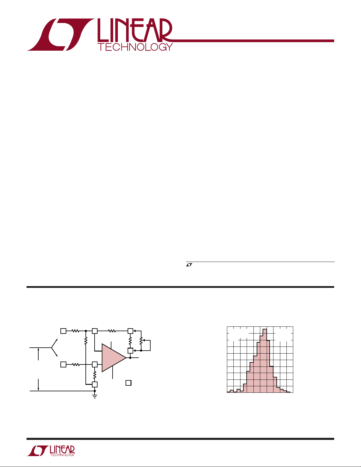
±250V Common Mode Range Instrumentation Amplifier (AV = 1)
R1
1M
3 4 1
–IN
R2
20k
R3
COMMON
MODE
INPUT
±250V
COMMON MODE REJECTION RATIO = 74dB (RESISTOR LIMITED)
WITH OPTIONAL TRIM = 130dB
OUTPUT OFFSET (TRIMMABLE TO ZERO) = 500µV
OUTPUT OFFSET DRIFT = 10µV/°C
INPUT RESISTANCE = 1M
+IN
1M
7
6
R4
19.608k
5
6V TO 18V
2
–
LT1012
3
+
–6V TO –18V
R5
975k
R6
25k
7
2
6
4
R1 TO R6: VISHAY 444
ACCUTRACT THIN FILM
SIP NETWORK
: VISHAY 444 PIN NUMBERS
X
VISHAY INTERTECHNOLOGY, INC
63 LINCOLN HIGHWAY
MALVERN, PA 19355
LT1012A • TA01
OUT
50k
OPTIONAL
CMRR
TRIM
Typical Distribution of Input
Offset Voltage
200
1140 UNITS
FROM THREE
RUNS
160
120
80
NUMBER OF UNITS
40
0
–40
–20
INPUT OFFSET VOLTAGE (µV)
0
VS = ±15V
= 25°C
T
A
V
CM
20 40
LT1012A • TA02
= 0V
sn1012 1012afbs
1
LT1012A/LT1012
WWWU
ABSOLUTE AXI U RATI GS
(Note 1)
Supply Voltage ......................................................± 20V
Differential Input Current (Note 1) ......................± 10mA
Input Voltage .........................................................± 20V
Output Short Circuit Duration .......................... Indefinite
UU
W
PACKAGE/ORDER I FOR ATIO
V
OS
TRIM
–IN
+IN
–
V
T
JMAX
TOP VIEW
1
2
–
3
+
4
S8 PACKAGE
8-LEAD PLASTIC SO
=
100°C, θJA = 170°C/W
V
OS
8
TRIM
+
7
V
6
OUT
OVER
5
COMP
V
OS
TRIM
1
2
–IN OUT
+IN OVER
H PACKAGE
8-LEAD TO-5 METAL CAN
= 150°C, θJA = 150°C/W, θJC = 45°C/W
T
JMAX
Operating Temperature Range
LT1012AM/LT1012M (OBSOLETE)....– 55°C to 125°C
LT1012I/LT1012AI ............................. – 40°C to 85°C
LT1012AC/LT1012C
LT1012D/LT1012S8 ................................ 0°C to 70°C
Storage Temperature Range ................. – 65°C to 150°C
Lead Temperature (Soldering, 10 sec).................. 300°C
TOP VIEW
V
OS
–
V
TRIM
8
–
+
4
(CASE)
7
53
+
V
6
COMP
V
OS
TRIM
–IN
+IN
V
TOP VIEW
1
2
–
3
–
T
+
4
N8 PACKAGE
8-LEAD PDIP
= 100°C, θJA = 130°C/W
JMAX
8
7
6
5
V
OS
TRIM
+
V
OUT
OVER
COMP
ORDER PART NUMBER
LT1012S8
LT1012IS8
LT1012ACS8
LT1012AIS8
ORDER PART NUMBER
LT1012AMH
LT1012MH
LT1012ACH
LT1012CH
LT1012DH
S8 PART MARKING
1012
1012I
1012A
1012AI
Consult LTC Marketing for parts specified with wider operating temperature ranges.
OBSOLETE PACKAGE
Consider the S8 or N8 Packages for Alternate Source
ORDER PART NUMBER
LT1012ACN8
LT1012AIN8
LT1012CN8
LT1012DN8
LT1012IN8
2
sn1012 1012afbs

LT1012A/LT1012
ELECTRICAL CHARACTERISTICS
SYMBOL PARAMETER CONDITIONS MIN TYP MAX MIN TYP MAX MIN TYP MAX UNITS
V
OS
I
OS
I
B
e
n
e
n
i
n
A
VOL
CMRR Common Mode Rejection VCM = ±13.5V 114 132 114 132 110 132 dB
PSRR Power SuppIy Rejection Ratio VS = ±1.2V to ±20V 114 132 114 132 110 132 dB
V
OUT
I
S
Input Offset Voltage 8 25 8 35 10 50 µV
(Note 3) 20 90 20 90 25 120 µV
Long Term lnput Offset 0.3 0.3 0.3 µV/month
Voltage Stability
Input Offset Current 15 100 15 100 20 150 pA
(Note 3) 25 150 25 150 30 200 pA
Input Bias Current ±25 ±100 ±25 ±100 ±30 ±150 pA
(Note 3) ±35 ±150 ±35 ±150 ±40 ±200 pA
Input Noise Voltage 0.1Hz to 10Hz 0.5 0.5 0.5 µV
Input Noise Voltage Density fO = 10Hz (Note 4) 17 30 17 30 17 30 nV√Hz
f
= 1000Hz (Note 5) 14 22 14 22 14 22 nV√Hz
O
Input Noise Current Density f
Large Signal Voltage Gain V
Ratio
Input Voltage Range ±13.5 ±14 ±13.5 ±14 ±13.5 ±14 V
Output Voltage Swing RL = 10kΩ±13 ±14 ±13 ±14 ±13 ±14 V
Slew Rate 0.1 0.2 0.1 0.2 0.1 0.2 V/µs
Supply Current 370 500 380 380 µA
10Hz 20 20 20 fA/√Hz
O =
= ±12V, RL ≥ 10kΩ 300 2000 300 2000 200 2000 V/mV
OUT
V
= ±10V, RL ≥ 2kΩ 300 1000 200 1000 200 1000 V/mV
OUT
(Note 3) 380 600 380 600 380 600 µA
VS = ± 15V, VCM = OV, TA = 25°C, unless otherwise noted.
LT1O12AM/AC/AI LT1O12M/I LT1O12C
P-P
sn1012 1012afbs
3

LT1012A/LT1012
ELECTRICAL CHARACTERISTICS
SYMBOL PARAMETER CONDITIONS MIN TYP MAX MIN TYP MAX UNITS
V
OS
l
OS
I
B
e
n
e
n
i
n
A
VOL
CMRR Common Mode Rejection Ratio VCM = ±13.5V 110 132 110 132 dB
PSRR Power Supply Rejection Ratio VS = ±1.2V to ± 20V 110 132 110 132 dB
V
OUT
I
S
Input Offset Voltage 12 60 15 120 µV
(Note 3) 25 25 180 µV
Long Term Input Offset 0.3 0.4 µV/month
Voltage Stability
Input Offset Current 20 150 50 280 pA
(Note 3) 30 60 380 pA
Input Bias Current ±30 ± 150 ±80 ±300 pA
(Note 3) ±40 ±120 ±400 pA
Input Noise Voltage 0.1Hz to 10Hz 0.5 0.5 µV
Input Noise Voltage Density fO = 10Hz (Note 5) 17 30 17 30 nV√Hz
f
= 1000Hz (Note 5) 14 22 14 22 nV√Hz
O
lnput Noise Current Density fO = 10Hz 20 20 fA/√Hz
Large-Signal Voltage Gain V
Input Voltage Range ±13.5 ±14.0 ±13.5 ±14.0 V
Output Voltage Swing RL = 10kΩ±13 ±14 ±13 ±14 V
Slew Rate 0.1 0.2 0.1 0.2 V/µs
Supply Current (Note 3) 380 600 380 600 µA
±12V,RL ≥ 10kΩ 200 2000 200 2000 V/mV
OUT =
±10V,RL ≥ 2kΩ 200 1000 120 1000 V/mV
V
OUT =
VS = ± 15V, VCM = 0V, TA = 25°C, unless otherwise noted.
LT1012D LT1012S8
P-P
4
sn1012 1012afbs

LT1012A/LT1012
ELECTRICAL CHARACTERISTICS
The ● denotes the specifications which apply over the full operating
temperature range of –55°C ≤ TA ≤ 125°C for LT1012AM and LT1012M, and –40°C ≤ TA≤ 85°C for LT1012AI and LT1012I.
VS = ± 15V, VCM = 0V, unless otherwise noted.
LT1012AM/AI LT1012M/I
SYMBOL PARAMETER CONDITIONS MIN TYP MAX MIN TYP MAX UNITS
V
OS
I
OS
I
B
A
VOL
CMRR Common Mode Rejection Ratio VCM = ±13.5V ● 110 128 108 128 dB
PSRR Power Supply Rejection Ratio VS = ±1.5V to ± 20V ● 110 126 108 126 dB
V
OUT
I
S
Input Offset Voltage ● 30 60 30 180 µV
(Note 3)
Average Temperature Coefficient of ● 0.2 0.6 0.2 1.5 µV/°C
Input Offset Voltage
Input Offset Current ● 30 250 30 250 pA
(Note 3)
Average Temperature Coefficient of ● 0.3 2.5 0.3 2.5 pA/°C
Input Offset Current
Input Bias Current ● ±80 ±600 ±80 ±600 pA
(Note 3)
Average Temperature Coefficient of ● 0.6 6.0 0.6 6.0 pA/°C
Input Bias Current
Large-Signal Voltage Gain V
Input Voltage Range ● ±13.5 ±13.5 V
Output Voltage Swing RL = 10kΩ ● ±13 ±14 ±13 ±14 V
Supply Current ● 400 650 400 800 µA
= ±12V, RL ≥ 10kΩ ● 200 1000 150 1000 V/mV
OUT
= ±10V, RL ≥ 2kΩ ● 200 600 100 600 V/mV
V
OUT
● 40 180 40 250 µV
● 70 350 70 350 pA
● ±150 ±800 ±150 ±800 pA
sn1012 1012afbs
5

LT1012A/LT1012
ELECTRICAL CHARACTERISTICS
The ● denotes the specifications which apply over the full operating
temperature range of 0°C ≤ TA ≤ 70°C. VS = ± 15V, VCM = 0V, unless otherwise noted.
SYMBOL PARAMETER CONDITIONS MIN TYP MAX MIN TYP MAX UNITS
V
OS
I
OS
I
B
A
VOL
CMRR Common Mode Rejection Ratio VCM = 13.5V ● 110 130 108 130 dB
PSRR Power Supply Rejection Ratio VS = ±1.3V to ± 20V ● 110 128 108 128 dB
V
OUT
I
S
Input Offset Voltage ● 20 60 20 100 µV
(Note 3)
Average Temperature Coefficient of ● 0.2 0.6 0.2 1.0 µV/°C
Input Offset Voltage
Input Offset Current ● 25 230 35 230 pA
(Note 3)
Average Temperature Coefficient of ● 0.3 2.5 0.3 2.5 pA/°C
Input Offset Current
Input Bias Current ● ± 35 ± 230 ± 35 ± 230 pA
(Note 3)
Average Temperature Coefficient of ● 0.3 2.5 0.3 2.5 pA/°C
Input Bias Current
Large-Signal Voltage Gain V
Input Voltage Range ● ±13.5 ±13.5 V
Output Voltage Swing RL = 10kΩ ● ±13 ±14 ±13 ±14 V
Supply Current ● 400 600 400 800 µA
= ±12V, RL ≥ 10kΩ ● 200 1500 150 1500 V/mV
OUT
= ±10V, RL ≥ 2kΩ ● 200 1000 150 800 V/mV
V
OUT
● 30 160 30 200 µV
● 40 300 45 300 pA
● ± 50 ± 300 ± 50 ± 300 pA
LT1012AC LT1012C
6
sn1012 1012afbs

LT1012A/LT1012
ELECTRICAL CHARACTERISTICS
The ● denotes the specifications which apply over the full operating
temperature range of 0°C ≤ TA ≤ 70°C. VS = ± 15V, VCM = 0V, unless otherwise noted.
SYMBOL PARAMETER CONDITIONS MIN TYP MAX MIN TYP MAX UNITS
V
OS
I
OS
I
B
A
VOL
CMRR Common Mode Rejection Ratio VCM = ±13.5V ● 108 130 108 130 dB
PSRR Power Supply Rejection Ratio VS = ±1.3V to ± 20V ● 108 128 108 128 dB
V
OUT
I
S
Input Offset Voltage ● 25 140 30 200 µV
(Note 3)
Average Temperature Coefficient of ● 0.3 1.7 0.3 1.8 µV/°C
Input Offset Voltage
Input Offset Current ● 35 380 60 380 pA
(Note 3)
Average Temperature Coefficient of ● 0.35 4.0 0.4 4.0 pA/°C
Input Offset Current
Input Bias Current ● ± 50 ± 420 ±100 ± 420 pA
(Note 3)
Average Temperature Coefficient of ● 0.4 5.0 0.5 5.0 pA/°C
Input Bias Current
Large-Signal Voltage Gain V
Input Voltage Range ● ±13.5 ±13.5 V
Output Voltage Swing RL = 10kΩ ● ±13 ±14 ±13 ±14 V
Supply Current ● 400 800 400 800 µA
= ±12V, RL ≥ 10kΩ ● 150 1500 150 1500 V/mV
OUT
= ±10V, RL ≥ 2kΩ ● 150 800 100 800 V/mV
V
OUT
● 40 45 270 µV
● 45 80 500 pA
● ± 65 ±150 ± 550 pA
LT1012D LT1012S8
Note 1: Absolute Maximum Ratings are those values beyond which the life
of a device may be impaired.
Note 2: Differential input voltages greater than 1V will cause excessive
current to flow through the input protection diodes unless limiting
resistance is used.
+
V
5k TO 100k POT
1
2
3
–
LT1012
+
V
8
7
6
OUT
5
4
–
C
S
LT1012A • EC01
Note 3: These specifications apply for V
≤ V
–13.5V
0°C to 70°C, ± 1.5V from – 55°C to 125°C.
Note 4: 10Hz noise voltage density is sample tested on every lot. Devices
100% tested at 10Hz are available on request.
Note 5: This parameter is tested on a sample basis only.
≤ 13.5V (for VS = ± 15V). V
CM
≤ VS ≤ ± 20V and
MIN
= ±1.2V at 25°C, ± 1.3V from
MIN
Optional Offset Nulling and Overcompensation
Circuits
Input offset voltage can be adjusted over a ± 800µV range
with a 5k to 100k potentiometer.
The LT1012 is internally compensated for unity gain
stability. The overcompensation capacitor, CS, can be
used to improve capacitive load handling capability, to
narrow noise bandwidth, or to stabilize circuits with gain
in the feedback loop.
sn1012 1012afbs
7

LT1012A/LT1012
UW
TYPICAL PERFOR A CE CHARACTERISTICS
Offset Voltage vs Source
Resistance (Balanced or
Unbalanced)
1000
V
= ±15V
S
100
Typical Distribution of Input Bias
Current
200
160
VS = ±15V
= 25°C
T
A
= 0V
V
CM
1020 UNITS
FROM THREE
RUNS
Typical Distribution of Input
Offset Current
200
VS = ±15V
T
= 25°C
A
= 0V
V
CM
160
1020 UNITS
FROM THREE
RUNS
–55°C TO 125°C
10
INPUT OFFSET VOLTAGE (µV)
1
1k
SOURCE RESISTANCE (Ω)
Input Bias Current vs
Temperature
100
50
0
–50
INPUT BIAS CURRENT (pA)
–100
–150
–50
UNDERCANCELLED UNIT
OVERCANCELLED
0
–25 25
TEMPERATURE (°C)
25°C
UNIT
120
80
NUMBER OF UNITS
40
0
–120
100k10k 300k 1M 3M 10M30k3k
LT1012A • TPC01
–60
INPUT BIAS CURRENT (pA)
0
60 120
LT1012A • TPC02
120
80
NUMBER OF UNITS
40
0
–120
INPUT OFFSET CURRENT (pA)
–60
0
60 120
LT1012A • TPC03
Offset Voltage Drift vs Source
Input Bias Current Over Common
Mode Range
60
VS = ±15V
= 25oC
T
A
40
20
0
–20
INPUT BIAS CURRENT (pA)
–40
50
75
100
125
LT1012A • TPC04
–60
–15
–10
COMMON MODE INPUT VOLTAGE
DEVICE WITH POSITIVE
INPUT CURRENT
R
IN CM
DEVICE WITH NEGATIVE
INPUT CURRENT
I
B
V
CM
–5 0 5
= 2 X 10¹²Ω
–
+
10 15
LT1012A * TPC5
Resistance (Balanced or
Unbalanced)
100
10
1.0
MAXIMUM
TYPICAL
0.1
1k
OFFSET VOLTAGE DRIFT WITH TEMPERATURE (µV/°C)
100k10k 1M 10M 100M
SOURCE RESISTANCE (Ω)
LT1012 • TPC06
8
Warm-Up Drift
5
= ±15V
V
S
= 25°C
T
A
4
3
2
1
CHANGE IN OFFSET VOLTAGE (µV)
0
0
METAL CAN (H) PACKAGE
DUAL-IN-LINE PACKAGE
PLASTIC (N) OR SO (S)
1
TIME AFTER POWER ON (MINUTES)
3
2
4
LT1012A • TPC07
Long Term Stability of Four
Representative Units
10
8
6
4
2
0
–2
–4
–6
CHANGE IN OFFSET VOLTAGE (µV)
–8
–10
5
1
0
TIME (MONTHS)
3
4
2
5
LT1012A • TPC08
Offset Voltage Drift with Temperature
of Four Representative Units
60
40
20
0
–20
OFFSET VOLTAGE (µV)
–40
–60
–50
–25 0
TEMPERATURE (°C)
50 100 125
25 75
LT1012A • TPC09
sn1012 1012afbs

LOAD RESISTANCE (kΩ)
1
100k
300k
1M
10M
3M
VOLTAGE GAIN
521020
VS = ±15V
V
0
= ±10V
25°C
125°C
–55°C
LT1012A • TPC18
TOTAL NOISE DENSITY (µV/√Hz)
SOURCE RESISTANCE (Ω)
10
2103104105106107
0.01
1.0
10.0
10
8
0.1
TA = 25°C
V
S
= ±1.2V TO ±20V
LT1012A • TPC12
RS = 2R
R
R
+
–
AT 10Hz
AT 1kHz
RESISTOR NOISE
ONLY
AT 10Hz
AT 1kHz
UW
TYPICAL PERFOR A CE CHARACTERISTICS
LT1012A/LT1012
0.1Hz to 10Hz Noise
TA = 25°C
V
= ±1.2V TO ± 20V
S
NOISE VOLTAGE 400nV/DIVISION
2
0
TIME (SECONDS)
6
4
Supply Current vs Supply Voltage
500
400
SUPPLY CURRENT (µA)
300
0
25°C
125°C
–55°C
±5
±10
SUPPLY VOLTAGE (V)
LT1012A • TPC10
±15
LT1012A • TPC13
Noise Spectrum
1000
TA = 25°C
= ±1.2 TO ±20V
V
S
100
CURRENT NOISE
VOLTAGE NOISE
10
1/f CORNER
2.5Hz
CURRENT NOISE DENSITY (fA√Hz)
VOLTAGE NOISE DENSITY (nV√Hz)
8
10
1
1
10 100 1000
FREQUENCY (Hz)
1/f CORNER
120Hz
LT1012A • TPC11
Common Mode Rejection vs
Frequency
140
120
100
80
60
40
20
VS = ±15V
COMMON MODE REJECTION RATIO (dB)
±20
= 25°C
T
A
0
1
10 100
FREQUENCY (Hz)
10k 1M
1k 100k
LT1012A • TPC14
Total Noise vs Source Resistance
Power Supply Rejection vs
Frequency
140
120
100
80
VS = ±15V
= 25°C
T
A
110
POSITIVE
SUPPLY
FREQUENCY (Hz)
60
40
POWER SUPPLY REJECTION RATIO (dB)
20
0.1
NEGATIVE
SUPPLY
1k 100k 1M
100 10k
LT1012A • TPC15
Voltage Gain vs Frequency Voltage Gain vs Load Resistance
140
120
100
80
60
40
VOLTAGE GAIN (dB)
20
VS = ±15V
0
= 25°C
T
A
–20
0.01
0.1
GAIN (dB)
1
100 1k 10k 100k 1M 10M
10
FREQUENCY (Hz)
LT1012A • TPC16
Gain, Phase Shift vs Frequency
40
30
20
GAIN
10
PHASE MARGIN
= 70°C
0
VS = ±15V
= 25°C
T
A
–10
0.01
0.1 1 10
FREQUENCY (MHz)
PHASE
LT1012A • TPC17
100
120
PHASE SHIFT (DEGREES)
140
160
180
200
sn1012 1012afbs
9

LT1012A/LT1012
UW
TYPICAL PERFOR A CE CHARACTERISTICS
Small-Signal Transient Response Large-Signal Transient Response
20mV/DIV
A
C
= +1
V
LOAD
= 100pF
5µs/DIV
Small-Signal Transient Response
20mV/DIV
A
C
= +1
V
LOAD
= 1000pF
5µs/DIV
2V/DIV
A
V
= +1
20µs/DIV
Slew Rate, Gain Bandwidth
Output Short-Circuit Current
vs Time
20
15
10
5
0
–5
–10
SHORT-CIRCUIT CURRENT (mA)
–15
SINKING SOURCING
–20
0
TIME FROM OUTPUT SHORT (MINUTES)
VS = ±15V
1
–55°C
25°C
125°C
125°C
25°C
–55°C
2
3
LT1012A • TPC19
Product vs Overcompensation
Capacitor Closed-Loop Output Impedance
1
GBW
SLEW
0.1
0.01
SLEW RATE (V/µs)
VS = ±15V
= 25°C
T
A
0.001
1 100 1000 10,000
10
OVERCOMPENSATION CAPACITOR (pF)
LT1012A • TPC20
1000
100
10
1
1000
GAIN BANDWIDTH PRODUCT (kHz)
100
10
1
0.1
OUTPUT IMPEDANCE (Ω)
0.01
0.001
10 100 1 10
1
AV = 1000
FREQUENCY (Hz)
A
V
T
I
V
= +1
= 1mA
0
= ±15V
S
= 25°C
A
LT1012A • TPC21
100
10
Common Mode Range and Voltage
Swing at Minimum Supply Voltage
+
V
+
– 0.3
V
+
– 0.6
V
+
– 0.9
V
+
– 1.2
V
–
+ 1.2
V
–
+ 0.9
V
–
V
+ 0.6
–
V
+ 0.3
–
V
COMMON MODE RANGE OR OUTPUT VOLTAGE (V)
–50
0 25 125
–25 100
TEMPERATURE (°C)
SWING R
SWING R
SWING R
50
CM RANGE
L
CM RANGE
75
= 2k
L
= 10k
= 2k
L
LT1012A • TPC22
Minimum Supply Voltage,
Voltage Gain at V
±1.8
±1.6
±1.4
±1.2
±1.0
±0.8
MINIMUM SUPPLY VOLTAGE (V)
–50
RL = 10k
RL = 2k
0
–25
TEMPERATURE (°C)
25
MIN
50
75
100
LT1012A • TPC23
400k
SUPPLY VOLTAGE (V/V)
300k
200k
100k
0
125
VOLTAGE GAIN AT MINIMUM
sn1012 1012afbs

WUUU
APPLICATIO S I FOR ATIO
LT1012A/LT1012
The LT1012 may be inserted directly into OP-07, LM11,
108A or 101A sockets with or without removal of external
frequency compensation or nulling components. The
LT1012 can also be used in 741, LF411, LF156 or OP-15
applications provided that the nulling circuitry is
removed.
Although the OP-97 is a copy of the LT1012, the LT1012
directly replaces and upgrades OP-97 applications. The
LT1012C and D have lower offset voltage and drift than the
OP-97F. The LT1012A has lower supply current than the
OP-97A/E. In addition, all LT1012 grades guarantee
operation at ±1.2V supplies.
Achieving Picoampere/Microvolt Performance
In order to realize the picoampere/microvolt level
accuracy of the LT1012, proper care must be exercised.
For example, leakage currents in circuitry external to
the op amp can significantly degrade performance. High
quality insulation should be used (e.g. Teflon, Kel-F);
cleaning of all insulating surfaces to remove fluxes and
other residues will probably be required. Surface coating
may be necessary to provide a moisture barrier in high
humidity environments.
Board leakage can be minimized by encircling the input
circuitry with a guard ring operated at a potential close
to that of the inputs: in inverting configurations the
guard ring should be tied to ground, in non-inverting
connections to the inverting input at Pin 2. Guarding both
sides of the printed circuit board is required. Bulk leakage
reduction depends on the guard ring width. Nanoampere
level leakage into the offset trim terminals can affect offset
voltage and drift with temperature.
OFFSET TRIM
+
V
8
OUTPUT
OVER COMP
7
4
GUARD
1
2
3
PUTS
IN
LT1012A * AI01
6
5
–
V
Microvolt level error voltages can also be generated in
the external circuitry. Thermocouple effects caused by
temperature gradients across dissimilar metals at the
contacts to the input terminals can exceed the inherent
drift of the amplifier. Air currents over device leads should
be minimized, package leads should be short, and the two
input leads should be as close together as possible and
maintained at the same temperature.
Noise Testing
For application information on noise testing and calculations, please see the LT1008 data sheet.
Frequency Compensation
The LT1012 can be overcompensated to improve
capacitive load handling capability or to narrow noise
bandwidth. In many applications, the feedback loop around
the amplifier has gain (e.g. Iogarithmic amplifiers);
overcompensation can stabilize these circuits with a single
capacitor.
The availability of the compensation terminal permits
the use of feedforward frequency compensation to
enhance slew rate. The voltage follower feedforward
scheme bypasses the amplifier’s gain stages and slews at
nearly 10V/µs.
The inputs of the LT1012 are protected with back-to-back
diodes. Current limiting resistors are not used, because
the leakage of these resistors would prevent the realization
of picoampere level bias currents at elevated temperatures. In the voltage follower configuration, when the input
is driven by a fast, large signal pulse (>1V), the input
protection diodes effectively short the output to the input
during slewing, and a current, limited only by the output
short-circuit protection will flow through the diodes.
The use of a feedback resistor, as shown in the voltage
follower feedforward diagram, is recommended because
this resistor keeps the current below the short-circuit
limit, resulting in faster recovery and settling of the output.
sn1012 1012afbs
11

LT1012A/LT1012
WUUU
APPLICATIO S I FOR ATIO
Test Circuit for Offset Voltage
and its Drift with Temperature
*
50k
15V
7
2
–
*
100Ω
*
50k
*RESISTORS MUST HAVE LOW THERMOELECTRIC
POTENTIAL
LT1012
3
+
–15V
V0 = 1000V
6
4
0S
V
0
LT1012A • AI02
TYPICAL APPLICATIO S
Follower Feedforward Compensation
50pF
10k
2
–
5k
IN
3
LT1012
+
0.01µF
5
U
Ampmeter with Six Decade Range
Pulse Response of Feedforward
Compensation
5V/DIV
6
OUT
LT1012A • AI03
Photoo
10k
5µs/DIV
15V
10k
CURRENT INPUT
Q1, Q2, Q3, Q4, RCA CA3146 TRANSISTOR ARRAY.
CALIBRATION: ADJUST R1 FOR FULL-SCALE
DEFLECTION WITH 1µA INPUT CURRENT
AMPMETER MEASURES CURRENTS FROM 100pA
TO 100µA WITHOUT THE USE OF EXPENSIVE
HIGH VALUE RESISTORS. ACCURACY AT 100µA
IS LIMITED BY THE OFFSET VOLTAGE BETWEEN
Q1 AND Q2 AND, AT 100pA, BY THE INVERTING
BIAS CURRENT OF THE LT1012
10k
Q3
1nA
R1
2k
1.2k
549Ω
549Ω
549Ω
549Ω
549Ω
549Ω
LT1004C
LT1012A • TA03
100µA
METER
0.1µF
15V
2
3
–
+
LT1012
–15V
7
6
4
PIN 13
CA3146
Q1
33k
Q4
100pA
RANGE
Q2
10nA
100nA
1µA
10µA
100µA
12
sn1012 1012afbs

TYPICAL APPLICATIO S
1.018235V
U
Saturated Standard Cell Amplifier
2N3609
3
+
2
–
+
SATURATED
STANDARD
CELL
#101
EPPLEY LABS
NEWPORT, R.I.
THE TYPICAL 30pA BIAS CURRENT OF THE LT1012 WILL
DEGRADE THE STANDARD CELL BY ONLY 1ppm/YEAR.
NOISE IS A FRACTION OF A ppm. UNPROTECTED GATE
MOSFET ISOLATES STANDARD CELL ON POWER DOWN
R1
LT1012
LT1008
–15V
R2
LT1012A/LT1012
15V
7
6
4
OUT
LT1012A • TA05
100k
100k
Amplifier for Bridge Transducers
R5
R6
56M
56M
2
–
LT1012
3
+
6
VOLTAGE GAIN ≈ 100
OUT
LT1012A • TA06
+
V
S1
T
100k
R1
S2
T
R2
100k
R3
510k
R4
510k
sn1012 1012afbs
13

LT1012A/LT1012
TYPICAL APPLICATIO S
R1
5M
1%
S1
λ
R2
5M
1%
2
–
LT1012
3
+
6
V
OUT =
U
10V/µA
LT1012A • TA07
OUT
15V
LM399
Buffered Reference for A-to-D ConvertersAmplifier for Photodiode Sensor
7k
3
2
6.5k
1k
7
+
LT1012
–
4
*THE 1k PRELOAD
MINIMIZES GLITCHES
INDUCED BY TRANSIENT
LOADS
1k
6
3k
200
2N3904
OUT
10V
1k*
LT1012A • TA08
Instrumentation Amplifier with ±100V Common Mode Range Low Power Comparator with <10µV Hysteresis
100k
100Ω
OUT
LT1012A • TA09
+IN
–IN
10k
10k
5V
1k
330k
7
2
–
LT1012
3
+
1
3
4
–5V
620k
6
100k
100k
OUT
2N3904
LT1012A • TA10
–IN
+IN
100M
100M
10M
15V
2
3
10M
7
–
LT1012
+
4
–15V
AV = 100
ALL RESISTORS 1% OR BETTER
6
14
sn1012 1012afbs

TYPICAL APPLICATIO S
Air Flow Detector Input Amplifier for 4.5 Digit Voltmeter
15V
R2
1
100k
2
3
–
+
LT1012
3
–15V
8
4
15V
+
R1
TYPE J
1k
–
COLD
JUNCTION
AT AMBIENT
MOUNT R1 IN AIRFLOW.
ADJUST R2 SO OUTPUT GOES
HIGH WHEN AIRFLOW STOPS
10M
U
7
6
LT1012A • TA11
OUT
IN
900k
90k
10k
9M
0.1V
1V
10V
100V
1000V
2
100k
5%
3
FN507
ALLEN BRADLEY
DECADE VOLTAGE
DIVIDER
LT1012A/LT1012
15V
7
–
LT1012
+
5
* RATIO MATCH ±0.01%
6
4
–15V
1000pF
0.1V
1V
10V
9k*
100V
TO 1V FULL SCALE
1000V
ANALOG TO DIGITAL
1k*
THIS APPLICATION REQUIRES LOW
BIAS CURRENT AND OFFSET VOLTAGE,
LOW NOISE, AND LOW DRIFT WITH
TIME AND TEMPERATURE
CONVERTER
LT1012A • TA12
“No Trims” 12-Bit Multiplying DAC Output AmplifierResistor Multiplier
R
DAC
FEEDBACK
I
OUT1
I
OUT2
WHEN THE REFERENCE INPUT DROPS TO 0.1V,
THE LEAST SIGNIFICANT BIT DECREASES TO
THE MICROVOLT/PICOAMPERE RANGE
2
–
LT1012
3
+
6
OUT
LT1012 • TA14
R
IN
1G
R1
10M
R2
1k
R3
100k
3
+
LT1012
2
–
R
IN
10k
= R1
6
V
OUT
R3
1 +
(
)
R2
LT1012 • TA13
REFERENCE IN
0.1V TO 10V
12-BIT CMOS
MULTIPLYING
sn1012 1012afbs
15

LT1012A/LT1012
W
SCHE ATIC DIAGRA
TRIM TRIM
1 8 5
800Ω 800Ω
22k 22k
–IN
+IN
Q7
Q5
2
Q9
Q10
3
Q8
30pF
Q6
Q16
Q13
SS
Q1
Q17
4.3k
–
V
4
W
1.5k
S
OVER
COMP
1.3k
Q15Q2
Q39
4.8k
1.3k 4.2k
Q14
2.5k
Q3
3.3k 3.3k
S
Q4
Q11
Q23
50k 1.5k
Q12
Q19Q18
Q22
Q21
Q24
3k
Q31
3.7k
20k
Q34 Q35
3.7k 16k3.7k
+
V
7
Q20
Q29
Q25
J1
Q33
Q32
Q36
320Ω
Q30
Q27
Q28
1.5k
Q26
Q40
1.5k
40Ω
Q37
Q38
330Ω
Q41
Q43
Q42
40Ω
100Ω
40Ω
OUT
6
LT1012A • SD01
16
sn1012 1012afbs

PACKAGE DESCRIPTIO
SEATING
PLANE
(0.254 – 1.143)
45°TYP
U
H Package
8-Lead TO-5 Metal Can (.200 Inch PCD)
(Reference LTC DWG # 05-08-1320)
.335 – .370
(8.509 – 9.398)
DIA
.305 – .335
(7.747 – 8.509)
.016 – .021**
(0.406 – 0.533)
PIN 1
.010 – .045*
.028 – .034
(0.711 – 0.864)
.040
(1.016)
MAX
.050
(1.270)
MAX
.027 – .045
(0.686 – 1.143)
GAUGE
PLANE
.200
(5.080)
TYP
LT1012A/LT1012
.165 – .185
(4.191 – 4.699)
REFERENCE
.500 – .750
(12.700 – 19.050)
PLANE
.110 – .160
(2.794 – 4.064)
INSULATING
STANDOFF
*
LEAD DIAMETER IS UNCONTROLLED BETWEEN THE REFERENCE PLANE
AND THE SEATING PLANE
**
FOR SOLDER DIP LEAD FINISH, LEAD DIAMETER IS
.016 – .024
(0.406 – 0.610)
OBSOLETE PACKAGE
H8(TO-5) 0.200 PCD 0801
sn1012 1012afbs
17

LT1012A/LT1012
PACKAGE DESCRIPTIO
U
N8 Package
8-Lead PDIP (Narrow .300 Inch)
(Reference LTC DWG # 05-08-1510)
.255 ± .015*
(6.477 ± 0.381)
.400*
(10.160)
MAX
876
5
12
.300 – .325
(7.620 – 8.255)
.065
(1.651)
.008 – .015
(0.203 – 0.381)
+.035
.325
–.015
+0.889
8.255
()
–0.381
NOTE:
1. DIMENSIONS ARE
*THESE DIMENSIONS DO NOT INCLUDE MOLD FLASH OR PROTRUSIONS.
MOLD FLASH OR PROTRUSIONS SHALL NOT EXCEED .010 INCH (0.254mm)
INCHES
MILLIMETERS
TYP
.045 – .065
(1.143 – 1.651)
.100
(2.54)
BSC
3
4
.130 ± .005
(3.302 ± 0.127)
.120
(3.048)
MIN
.018 ± .003
(0.457 ± 0.076)
.020
(0.508)
MIN
N8 1002
18
sn1012 1012afbs

PACKAGE DESCRIPTIO
.050 BSC
N
U
S8 Package
8-Lead Plastic Small Outline (Narrow .150 Inch)
(Reference LTC DWG # 05-08-1610)
.189 – .197
.045 ±.005
(4.801 – 5.004)
8
NOTE 3
7
LT1012A/LT1012
5
6
.245
MIN
1 2 3 N/2
.030 ±.005
TYP
RECOMMENDED SOLDER PAD LAYOUT
.010 – .020
(0.254 – 0.508)
.008 – .010
(0.203 – 0.254)
NOTE:
1. DIMENSIONS IN
2. DRAWING NOT TO SCALE
3. THESE DIMENSIONS DO NOT INCLUDE MOLD FLASH OR PROTRUSIONS.
MOLD FLASH OR PROTRUSIONS SHALL NOT EXCEED .006" (0.15mm)
×
45
.016 – .050
(0.406 – 1.270)
INCHES
(MILLIMETERS)
.160
±.005
°
0°– 8° TYP
.228 – .244
(5.791 – 6.197)
.053 – .069
(1.346 – 1.752)
.014 – .019
(0.355 – 0.483)
TYP
N
.150 – .157
(3.810 – 3.988)
N/2
1
3
2
NOTE 3
4
.004 – .010
(0.101 – 0.254)
.050
(1.270)
BSC
SO8 0502
Information furnished by Linear Technology Corporation is believed to be accurate and reliable.
However, no responsibility is assumed for its use. Linear Technology Corporation makes no representation that the interconnection of its circuits as described herein will not infringe on existing patent rights.
sn1012 1012afbs
19

LT1012A/LT1012
TYPICAL APPLICATIO
U
Kelvin-Sensed Platinum Temperature Sensor Amplifier
10V
REFERENCE
LT1021-10
R2
100k
–15V
10M
392k*
235k*
5k*
ROSEMOUNT
EQUIVALENT
R1
5k
78S
OR
100Ω
AT
R
S
0°C
182k
4.75k
*
R
6.65M
2
200k
3
619k
F
654k
20V
7
–
LT1012
+
–15V
* = WIRE WOUND RESISTORS
ALL OTHER RESISTORS ARE 1% METAL FILM
TRIM R2 AT 0°C FOR V
TRIM R3 AT 100°C FOR V
TRIM R4 AT 50°C FOR V
IN THE ORDER INDICATED
POSITIVE FEEDBACK (R1) LINEARIZES THE
INHERENT PARABOLIC NONLINEARITY OF
THE PLATINUM SENSOR AND REDUCES
ERRORS FROM 1.2°C TO 0.004°C OVER
THE –50°C TO 150°C RANGE
6
4
= 0V
0
0
R3
1k
V
–50°C TO 150°C
= 10V
0
= 5V
24.3k
= 100mV/°C
OUT
R4
5k
LT1012A • TA04
10k
20
Linear Technology Corporation
1630 McCarthy Blvd., Milpitas, CA 95035-7417
(408) 432-1900 ● FAX: (408) 434-0507
●
www.linear.com
sn1012 1012afbs
LW/TP 1202 1K REV B • PRINTED IN USA
LINEAR TECHNOLOGY CORPORATION 1991
 Loading...