

Page 1
FEATURES
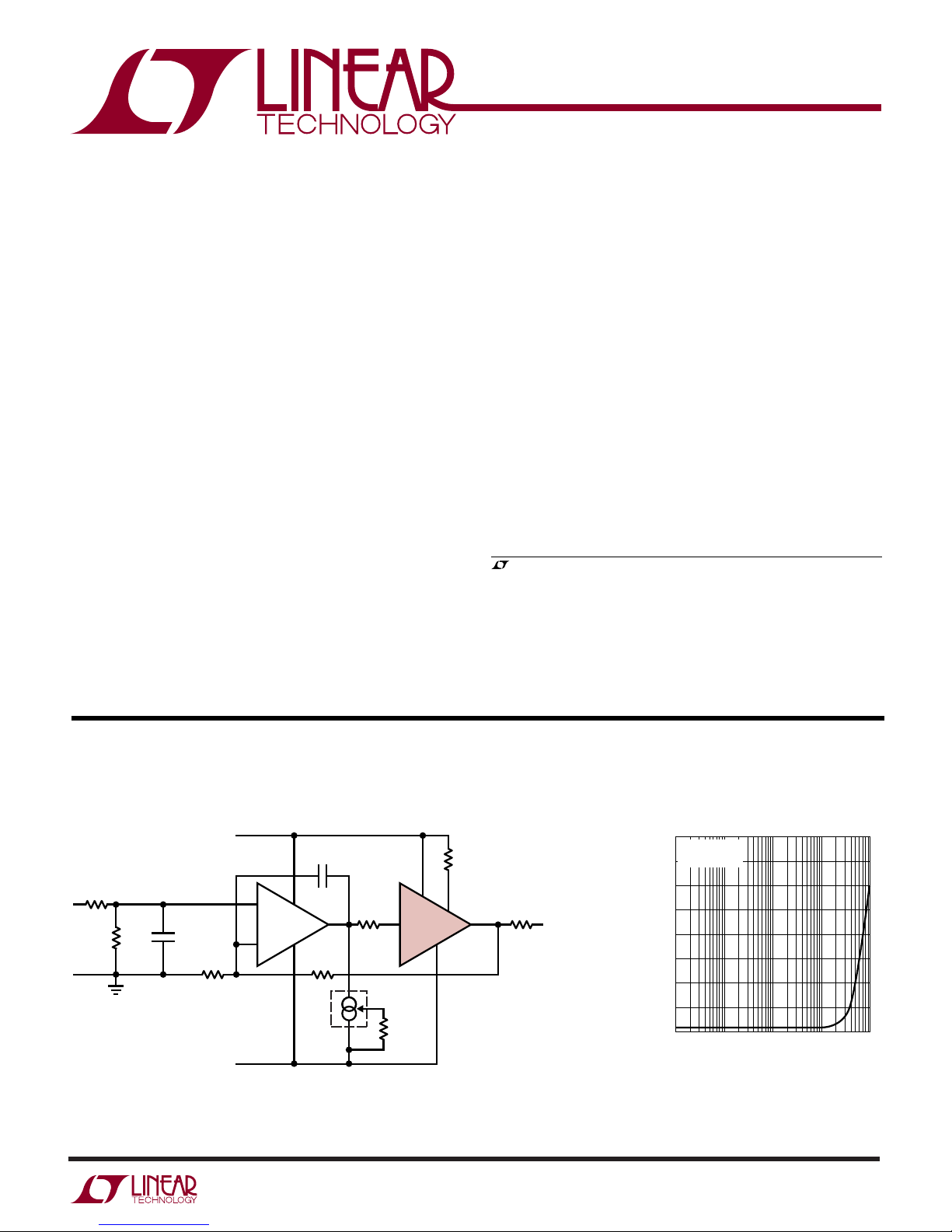
FREQUENCY (Hz)
0.1
HARMONIC DISTORTION (%)
0.2
0.4
10 1k 10k 100k
1010 TA02
0
100
0.3
V
OUT
= 10V
P-P
RL = 400Ω
LT1010
Fast ±150mA Power Buffer
U
DESCRIPTIO
■
20MHz Bandwidth
■
75V/µs Slew Rate
■
Drives ±10V into 75Ω
■
5mA Quiescent Current
■
Drives Capacitive Loads > 1µF
■
Current and Thermal Limit
■
Operates from Single Supply ≥ 4.5V
■
Very Low Distortion Operation
■
Available in 8-Pin miniDIP, Plastic TO-220
and Tiny 3mm × 3mm × 0.75mm 8-Pin DFN
Packages
U
APPLICATIO S
■
Boost Op Amp Output
■
Isolate Capacitive Loads
■
Drive Long Cables
■
Audio Amplifiers
■
Video Amplifiers
■
Power Small Motors
■
Operational Power Supply
■
FET Driver
The LT®1010 is a fast, unity-gain buffer that can increase
the output capability of existing IC op amps by more than
an order of magnitude. This easy-to-use part makes fast
amplifiers less sensitive to capacitive loading and reduces
thermal feedback in precision DC amplifiers.
Designed to be incorporated within the feedback loop, the
buffer can isolate almost any reactive load. Speed can be
improved with a single external resistor. Internal operating currents are essentially unaffected by the supply
voltage range. Single supply operation is also practical.
This monolithic IC is supplied in 8-pin miniDIP, plastic
TO-220 and 8-pin DFN packages. The low thermal resistance power package is an aid in reducing operating
junction temperatures.
, LT, LTC and LTM are registered trademarks of Linear Technology Corporation.
All other trademarks are the property of their respective owners.
TYPICAL APPLICATIO
Very Low Distortion Buffered Preamplifier
+
V
18V
R1
1k
R2
1M
NOTE 1: ALL RESISTORS 1% METAL FILM
NOTE 2: SUPPLIES WELL BYPASSED AND LOW Z
C1
22pF
R3
1k
–18V
3
+
LT1056CN8 LT1010CT
2
–
+
V
C2
22pF
7
4
R4
10k
LM334
O
I
= 2mA
SET
U
R7
50Ω
+
R6
100Ω
6
+
V
–
V
V
IN OUT
R
SET
33.2Ω
1%
BOOST
–
V
1010 TA01
R8
100Ω
OUTPUT
1010fc
1
Page 2
LT1010
WWWU
ABSOLUTE AXI U RATI GS
(Note 1)
Total Supply Voltage .............................................. ± 22V
Continuous Output Current .............................. ±150mA
Input Current (Note 3) ....................................... ±40mA
Operating Junction Temperature Range
LT1010C ............................................... 0°C to 100°C
Storage Temperature Range ................. –65°C to 150°C
Lead Temperature (Soldering, 10 sec).................. 300°C
UU
W
PACKAGE/ORDER I FOR ATIO
TOP VIEW
NC
V
+
1
2
3
4
N8 PACKAGE
8-LEAD PDIP
TOP VIEW
+
1V
BIAS
2
OUT
3
NC
4
8-LEAD (3mm × 3mm) PLASTIC DFN
T
JMAX
EXPOSED PAD (PIN 9) V
TO REDUCE THERMAL RESISTANCE (NOTE 7)
DD PACKAGE
= 100°C, θJC = 3°C/W, θJA = 40°C/W
–
CAN BE SOLDERED TO PCB
8
INPUT
NC
7
9
V
6
NC
5
–
BIAS
OUT
T
= 100°C, θJC = 45°C/W, θJA = 100°C/W
JMAX
U
UU
PRECO DITIO I G
100% Thermal Limit Burn In–LT1010CT
FRONT VIEW
8
INPUT
7
NC
–
6
V
5
NC
–
V
5-LEAD PLASTIC TO-220
T
= 125°C, θJC = 3°C/W, θJA = 50°C/W
JMAX
5
4
3
2
1
T PACKAGE
OUTPUT
BIAS
–
(TAB)
V
+
V
INPUT
ORDER PART
NUMBER
LT1010CDD LBWZ
DD PART
MARKING
ORDER PART
NUMBER
ORDER PART
NUMBER
LT1010CN8 LT1010CT
Order Options Tape and Reel: Add #TR
Lead Free: Add #PBF Lead Free Tape and Reel: Add #TRPBF
Lead Free Part Marking: http://www.linear.com/leadfree/
Consult LTC Marketing for parts specified with wider operating temperature ranges.
ELECTRICAL CHARACTERISTICS
temperature range, otherwise specifications are at T
The ● indicates specifications which apply over the full operating
= 25°C. (See Note 4. Typical values in curves.)
A
SYMBOL PARAMETER CONDITIONS (Note 4) MIN TYP MAX UNITS
V
OS
Output Offset Voltage (Note 4) 0 150 mV
●
–20 220 mV
VS = ± 15V, VIN = 0V 20 100 mV
I
B
A
V
R
OUT
Input Bias Current I
Large-Signal Voltage Gain
Output Resistance I
= 0mA 0 250 µA
OUT
≤ 150mA 0 500 µA
I
OUT
= ±1mA 5 10 Ω
OUT
I
= ±150mA 5 10 Ω
OUT
●
●
●
0 800 µA
0.995 1.00 V/V
12 Ω
Slew Rate VS = ±15V, VIN = ±10V, 75 V/µs
= ±8V, RL = 100Ω
V
OUT
1010fc
2
Page 3
LT1010
ELECTRICAL CHARACTERISTICS
temperature range, otherwise specifications are at T
The ● indicates specifications which apply over the full operating
= 25°C. (See Note 4. Typical values in curves.)
A
SYMBOL PARAMETER CONDITIONS (Note 4) MIN TYP MAX UNITS
+
V
SOS
V
SOS
R
SAT
V
BIAS
I
S
Note 1: Stresses beyond those listed under Absolute Maximum Ratings
may cause permanent damage to the device. Exposure to any Absolute
Maximum Rating condition for extended periods may affect device
reliability and lifetime.
Note 2: For case temperatures above 25°C, dissipation must be derated
based on a thermal resistance of 25°C/W for the T package, 130°C/W for
the N8 package and 40°C/W for the DD package for
above 25°C. See Applications Information.
Note 3: In current limit or thermal limit, input current increases sharply
with input-output differentials greater than 8V; so input current must be
limited. Input current also rises rapidly for input voltages 8V above V
0.5V below V
Note 4: Specifications apply for 4.5V ≤ V
–
+ 0.5V ≤ VIN ≤ V+ – 1.5V and I
V
Temperature range is 0°C ≤ T
Positive Saturation Offset I
–
Negative Saturation Offset I
Saturation Resistance I
Bias Terminal Voltage R
Supply Current I
–
.
≤ 40V,
S
= 0, unless otherwise stated.
OUT
≤ 100°C, TC ≤ 100°C.
J
ambient
= 0 (Note 5) 1.0 V
OUT
= 0 (Note 5) 0.2 V
OUT
= ±150mA (Note 5) 22 Ω
OUT
= 20Ω (Note 6) 700 840 mV
BIAS
OUT
= 0, I
= 0 9 mA
BIAS
●
●
●
●
560 880 mV
●
1.1 V
0.3 V
28 Ω
10 mA
Note 5: The output saturation characteristics are measured with 100mV
output clipping. See Applications Information for determining available
output swing and input drive requirements for a given load.
Note 6: The output stage quiescent current can be increased by
connecting a resistor between the BIAS pin and V
+
. The increase is
equal to the bias terminal voltage divided by this resistance.
temperatures
Note 7: Thermal resistance varies depending upon the amount of PC board
metal attached to the pin (Pin 9) of the device. θ
is specified for a certain
JA
amount of 1oz copper metal trace connecting to Pin 9 as described in the
+
or
thermal resistance tables in the Applications Information section.
1010fc
3
Page 4
LT1010
FREQUENCY (MHz)
25
5
10
PHASE LAG (DEGREES)
20
50
10 20
1010 G03
RL = 50Ω
R
L
= 200Ω
CL = 100pF
R
S
= 50Ω
R
BIAS
= 20Ω
T
J
= 25°C
UW
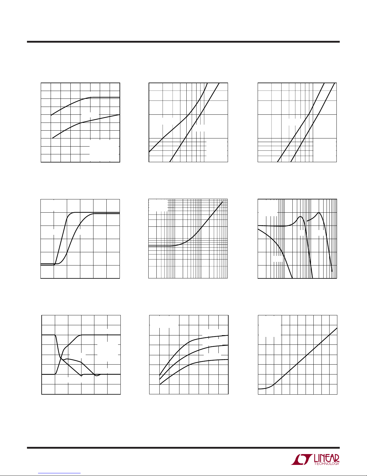
TYPICAL PERFOR A CE CHARACTERISTICS
Bandwidth Phase Lag Phase Lag
50
50
40
30
20
FREQUENCY (MHz)
10
0
0
QUIESCENT CURRENT (mA)
10
RL = 200Ω
RL = 50Ω
20
= 100mV
V
IN
CL 100pF
= –3dB
A
V
= 25°C
T
J
30
P-P
1010 G01
20
RL = 50Ω
10
PHASE LAG (DEGREES)
5
40
25
Small-Step Response Output Impedance
150
RL = 100Ω
= 25°C
T
J
100
50
INPUT OUTPUT
0
–50
VOLTAGE CHANGE (mV)
–100
100
I
= 0
BIAS
= 25°C
T
J
10
OUTPUT IMPEDANCE (Ω)
R
= 200Ω
L
FREQUENCY (MHz)
CL = 100pF
= 50Ω
R
S
= 0
I
BIAS
= 25°C
T
J
10 20
1010 G02
Capacitive Loading
10
RS = 50Ω
= 0
I
BIAS
= 25°C
T
J
0
–10
VOLTAGE GAIN (dB)
0.1µF
100pF3nF
–150
0
10 20
TIME (ns)
30
1010 G04
Slew Response
20
15
POSITIVE
VS = ±15V
= 100Ω
R
L
= 25°C
T
J
f ≤ 1MHz
NEGATIVE
200
1010 G07
250
10
5
0
–5
OUTPUT VOLTAGE (V)
–10
–15
–20
–50
4
0 50 150
= 0
I
BIAS
R
= 20Ω
BIAS
100
TIME (ns)
1
0.1
Negative Slew Rate
400
VS = ±15V
≥ –10V
0 ≥ V
IN
300
200
SLEW RATE (V/µs)
100
0
0
10
QUIESCENT CURRENT (mA)
1 10 100
FREQUENCY (MHz)
20
1010 G05
RL = 200Ω
RL = 100Ω
RL = 50Ω
30
1010 G08
–20
0.1
1 10 100
FREQUENCY (MHz)
1010 G06
Supply Current
80
VS = ±15V
= ±10V
V
IN
= 0
I
L
= 25°C
T
C
60
40
SUPPLY CURRENT (mA)
20
40
0
123 5
0
FREQUENCY (MHz)
4
1010 G09
1010fc
Page 5
UW
FREQUENCY (Hz)
10
100
NOISE VOLTAGE (nV/√Hz)
150
200
100 1k 10k
1010 G15
50
0
TJ = 25°C
RS = 1k
RS = 50Ω
TYPICAL PERFOR A CE CHARACTERISTICS
Output Offset Voltage Input Bias Current Input Bias Current
200
VIN = 0
200
VIN = 0
200
VS = ±15V
= 75Ω
R
L
LT1010
150
100
OFFSET VOLTAGE (mV)
50
0
–50
0
V+ = 38V
–
= –2V
V
+
V
–
V
50
TEMPERATURE (°C)
= 2V
= –38V
100
150
1010 G10
150
100
BIAS CURRENT (µA)
50
0
–50
Voltage Gain Output Resistance
1.000
0.999
GAIN (V/V)
0.998
I
OUT
= 0
VS = 40V
VS = 4.5V
12
I
≤ 150mA
OUT
10
8
6
4
OUTPUT RESISTANCE (Ω)
2
V+ = 38V
–
= –2V
V
0
50
TEMPERATURE (°C)
+
V
–
V
= 2V
= –38V
100
1010 G10
150
150
100
BIAS CURRENT (µA)
50
0
–100 –50 50
–150
OUTPUT CURRENT (mA)
Output Noise Voltage
0
TJ = 125°C
TJ = 25°C
TJ = –55°C
100
150
1010 G12
0.997
–50
Positive Saturation Voltage
4
3
2
1
SATURATION VOLTAGE (V)
0
–50
050
TEMPERATURE (°C)
IL = 150mA
IL = 50mA
IL = 5mA
0
50
TEMPERATURE (°C)
100
100
1010 G13
1010 G16
150
150
0
–50
050
TEMPERATURE (°C)
100
150
1010 G14
Negative Saturation Voltage Supply Current
4
3
2
1
SATURATION VOLTAGE (V)
0
–50
IL = –150mA
IL = –50mA
IL = –5mA
0
TEMPERATURE (°C)
50
100
150
1010 G16
7
VIN = 0
I
OUT
I
BIAS
6
5
SUPPLY CURRENT (mA)
4
3
0
= 0
= 0
10
TOTAL SUPPLY VOLTAGE (V)
TJ = –55°C
TJ = 25°C
TJ = 125°C
20
30
40
1010 G18
1010fc
5
Page 6

LT1010
TEMPERATURE (°C)
–50
0
OUTPUT CURRENT (A)
0.2
0.5
0
50
1010 G24
0.1
0.4
0.3
100
150
VS = ±15V
V
OUT
= 0
SINK
SOURCE
UW
TYPICAL PERFOR A CE CHARACTERISTICS
Bias Terminal Voltage Total Harmonic Distortion Total Harmonic Distortion
1.0
0.9
VS = ±20V
0.4
0.3
RL = 50Ω
f = 10kHz
= ±15V
V
S
= 25°C
T
C
0.8
0.6
I
BIAS
V
S
V
OUT
= 25°C
T
C
= 0
= ±15V
= ±10V
0.8
R
0.7
0.6
BIAS TERMINAL VOLTAGE (V)
0.5
–50
BIAS
0
TEMPERATURE (°C)
= 20Ω
R
= 100Ω
BIAS
50
100
150
1010 G19
0.2
0.1
HARMONIC DISTORTION (%)
0
0.1
I
= 0 R
BIAS
1 10 100
OUTPUT VOLTAGE (V
Shorted Input Characteristics Peak Power Capability
50
VS = ±15V
= 0
V
OUT
= 25°C
T
J
25
0
INUPT CURRENT (mA)
–25
–50
–10 –5 5
–15
0
INPUT VOLTAGE (V)
10
15
1010 G22
10
TC = 85°C
8
6
4
PEAK POWER (W)
2
0
1
PULSE WIDTH (ms)
= 50Ω
BIAS
)
P-P
1010 G20
TO-220
10 100
1010 G23
0.4
0.2
HARMONIC DISTORTION (%)
0
1
RL = 50Ω
RL = 100Ω
10 100 1000
FREQUENCY (kHz)
Peak Output Current
1010 G21
6
1010fc
Page 7

WUUU
V
VV R
RR
OUT
SOS L
SAT L
+
+
+
=
+
(– )
APPLICATIO S I FOR ATIO
LT1010
General
These notes briefly describe the LT1010 and how it is
1
used; a detailed explanation is given elsewhere
. Emphasis here will be on practical suggestions that have resulted
from working extensively with the part over a wide range
of conditions. A number of applications are also outlined
that demonstrate the usefulness of the buffer beyond that
of driving a heavy load.
Design Concept
The schematic below describes the basic elements of the
buffer design. The op amp drives the output sink transistor, Q3, such that the collector current of the output
follower, Q2, never drops below the quiescent value (determined by I
and the area ratio of D1 and D2). As a result,
1
the high frequency response is essentially that of a simple
follower even when Q3 is supplying the load current. The
internal feedback loop is isolated from the effects of
capacitive loading by a small resistor in the output lead.
+
V
D1
–
A1
I
1
D2
BIAS
I
+
Q2
R1
Q3
2
INPUT
Q1
OUTPUT
–
V
1010 AI01
idealized buffer with the unloaded gain specified for the
LT1010. Otherwise, it has zero offset voltage, bias current
and output resistance. Its output also saturates to the
internal supply terminals2.
+
V
+
V
A1
V
SOS
R′
R′ R′ = R
V
SOS
–
R
OUT
OUTPUTINPUT
– R
SAT
OUT
–
1010 AI02
I
B
V
OS
+
Loaded voltage gain can be determined from the unloaded
gain, A
tance, R
, the output resistance, R
V
, using:
L
AR
A
VL
VL
=
RR
+
OUT L
, and the load resis-
OUT
Maximum positive output swing is given by:
The input swing required for this output is:
R
OUT
R
L
⎞
+ ∆1–
VV
OS OS
⎟
⎠
+
VV
=+
IN OUT
⎛
+
⎜
⎝
The scheme is not perfect in that the rate of rise of sink
current is noticeably less than for source current. This can
be mitigated by connecting a resistor between the bias
terminal and V+, raising quiescent current. A feature of the
final design is that the output resistance is largely independent of the follower quiescent current or the output load
current. The output will also swing to the negative rail,
which is particularly useful with single supply operation.
Equivalent Circuit
Below 1MHz, the LT1010 is quite accurately represented
by the equivalent circuit shown here for both small- and
large-signal operation. The internal element, A1, is an
where ∆VOS is the 100mV clipping specified for the
saturation measurements. Negative output swing and
input drive requirements are similarly determined.
Supply Bypass
The buffer is no more sensitive to supply bypassing than
slower op amps as far as stability is concerned. The 0.1µF
disc ceramic capacitors usually recommended for op
amps are certainly adequate for low frequency work. As
always, keeping the capacitor leads short and using a
1
R. J. Widlar, “Unique IC Buffer Enhances Op Amp Designs; Tames Fast Amplifiers,”
Linear Technology Corp. TP-1
2
See electrical characteristics section for guaranteed limits.
, April, 1984.
1010fc
7
Page 8

LT1010
∆ =
+
I
VV
RR
OUT
OS OS
OUT OUT
12
12
–
WUUU
APPLICATIO S I FOR ATIO
ground plane is prudent, especially when operating at high
frequencies.
The buffer slew rate can be reduced by inadequate supply
bypass. With output current changes much above
100mA/µs, using 10µF solid tantalum capacitors on both
supplies is good practice, although bypassing from the
positive to the negative supply may suffice.
When used in conjunction with an op amp and heavily
loaded (resistive or capacitive), the buffer can couple into
supply leads common to the op amp causing stability
problems with the overall loop and extended settling time.
Adequate bypassing can usually be provided by 10µF solid
tantalum capacitors. Alternately, smaller capacitors could
be used with decoupling resistors. Sometimes the op amp
has much better high frequency rejection on one supply,
so bypass requirements are less on this supply.
Power Dissipation
In many applications the LT1010 will require heat sinking. Thermal resistance, junction to still air is 100°C/W
for the TO-220 package and 130°C/W for the miniDIP
package. Circulating air, a heat sink or mounting the
package to a printed circuit board will reduce thermal
resistance.
In DC circuits, buffer dissipation is easily computed. In AC
circuits, signal waveshape and the nature of the load
determine dissipation. Peak dissipation can be several
times average with reactive loads. It is particularly important to determine dissipation when driving large load
capacitance.
without limiting. Because of this, it is capable of power
dissipation in excess of its continuous ratings.
Normally, thermal overload protection will limit dissipation and prevent damage. However, with more than 30V
across the conducting output transistor, thermal limiting
is not quick enough to ensure protection in current limit.
The thermal protection is effective with 40V across the
conducting output transistor as long as the load current is
otherwise limited to 150mA.
Drive Impedance
When driving capacitive loads, the LT1010 likes to be
driven from a low source impedance at high frequencies.
Certain low power op amps (e.g., the LM10) are marginal
in this respect. Some care may be required to avoid
oscillations, especially at low temperatures.
Bypassing the buffer input with more than 200pF will solve
the problem. Raising the operating current also works.
Parallel Operation
Parallel operation provides reduced output impedance,
more drive capability and increased frequency response
under load. Any number of buffers can be directly paralleled as long as the increased dissipation in individual
units caused by mismatches of output resistance and
offset voltage is taken into account.
When the inputs and outputs of two buffers are connected
together, a current, ∆I
, flows between the outputs:
OUT
With AC loading, power is divided between the two output
transistors. This reduces the effective thermal resistance,
junction to case to 15°C/W for the TO-220 package as long
as the peak rating of neither output transistor is exceeded.
The typical curves indicate the peak dissipation capabilities of one output transistor.
Overload Protection
The LT1010 has both instantaneous current limit and
thermal overload protection. Foldback current limiting has
not been used, enabling the buffer to drive complex loads
8
where VOS and R
resistance of the respective buffers.
Normally, the negative supply current of one unit will
increase and the other decrease, with the positive supply
current staying the same. The worst-case (V
increase in standby dissipation can be assumed to be
∆I
Offset voltage is specified worst case over a range of
supply voltages, input voltage and temperature. It would
, where VT is the total supply voltage.
OUTVT
are the offset voltage and output
OUT
→ V+)
IN
1010fc
Page 9

WUUU
A2
LT1010
R
F
2k
R
S
2k
V
IN
C
F
1nF
C
L
1010 AI06
V
OUT
–
+
A1
LT118A
APPLICATIO S I FOR ATIO
LT1010
be unrealistic to use these worst-case numbers above
because paralleled units are operating under identical
conditions. The offset voltage specified for V
V
= 0V and TA = 25°C will suffice for a worst-case
IN
= ±15V,
S
condition.
+
V
I
S
IS – ∆I
A1
LT1010
OUT
–
V
V
IN
A2
LT1010
1010 AI03
I
S
IS + ∆I
OUT
V
OUT
∆I
OUT
Output load current will be divided based on the output
resistance of the individual buffers. Therefore, the available output current will not quite be doubled unless output
resistances are matched. As for offset voltage, the 25°C
limits should be used for worst-case calculations.
At lower frequencies, the buffer is within the feedback loop
so that its offset voltage and gain errors are negligible. At
higher frequencies, feedback is through C
, so that phase
F
shift from the load capacitance acting against the buffer
output resistance does not cause loop instability.
Stability depends upon the RFCF time constant or the
closed-loop bandwidth. With an 80kHz bandwidth, ringing is negligible for C
= 0.33µF. The pulse response is shown in the graph.
C
L
5
0
–5
5
OUTPUT VOLTAGE (V)
0
–5
0
= 0.068µF and damps rapidly for
L
Pulse Response
CL = 0.068µF
CL = 0.33µF
50
100
TIME (µs)
150
200
1010 AI05
Parallel operation is not thermally unstable. Should one
unit get hotter than its mates, its share of the output and
its standby dissipation will decrease.
As a practical matter, parallel connection needs only some
increased attention to heat sinking. In some applications,
a few ohms equalization resistance in each output may be
wise. Only the most demanding applications should require matching, and then just of output resistance at 25°C.
Isolating Capacitive Loads
The inverting amplifier below shows the recommended
method of isolating capacitive loads. Noninverting amplifiers are handled similarly.
R
S
V
IN
C
F
100pF
–
A1
LT1007
+
R
F
20k
A2
LT1010
C
L
1010 AI04
Small-signal bandwidth is reduced by CF, but considerable isolation can be obtained without reducing it below
the power bandwidth. Often, a bandwidth reduction is
desirable to filter high frequency noise or unwanted
signals.
The follower configuration is unique in that capacitive
load isolation is obtained without a reduction in smallsignal bandwidth, although the output impedance of the
V
OUT
buffer comes into play at high frequencies. The precision
unity-gain buffer above has a 10MHz bandwidth without
capacitive loading, yet it is stable for all load capacitance
to over 0.3µF, again determined by R
FCF
.
1010fc
9
Page 10

LT1010
A2
LT1010
R1
100Ω
R2
800Ω
C1
15pF
V
IN
1010 AI09
V
OUT
–
+
A1
HA2625
A2
LT1010
R1
400Ω
R2
1.6k
INPUT
1010 AI10
OUTPUT
–
+
A1
HA2625
WUUU
APPLICATIO S I FOR ATIO
This is a good example of how fast op amps can be made
quite easy to use by employing an output buffer.
Integrator
A lowpass amplifier can be formed just by using large C
F
in the inverter described earlier, as long as the increasing
closed-loop output impedance above the cutoff frequency
is not a problem and the op amp is capable of supplying
the required current at the summing junction.
C
I
I
IN
R
20k
F
–
LT1012
+
A1
C
F
500pF
A2
LT1010
1010 AI07
V
OUT
If the integrating capacitor must be driven from the buffer
output, the circuit above can be used to provide capacitive
load isolation. As before, the stability with large capacitive
loads is determined by R
FCF
.
Wideband Amplifiers
This simple circuit provides an adjustable gain video
amplifier that will drive 1V
into 75Ω. The differential
P-P
pair provides gain with the LT1010 serving as an output
8.2k
+
22µF
15V
25Ω
BIAS
22µF
TYPICAL SPECIFICATIONS
INTO 75Ω
1V
P-P
AT A = 2
0.5dB TO 10MHz
3dB DOWN AT 16MHz
AT A = 10
0.5dB TO 4MHz
+
–3dB = 8MHz
stage. Feedback is arranged in the conventional manner,
although the 68µF-0.01µF combination limits DC gain to
unity for all gain settings. For applications sensitive to
NTSC requirements, dropping the 25Ω output stage bias
value will aid performance.
This shows the buffer being used with a wideband amplifier that is not unity-gain stable. In this case, C1 cannot be
used to isolate large capacitive loads. Instead, it has an
optimum value for a limited range of load capacitances.
The buffer can cause stability problems in circuits like
this. With the TO-220 packages, behavior can be improved by raising the quiescent current with a 20Ω
+
resistor from the bias terminal to V
. Alternately, devices
in the miniDIP can be operated in parallel.
It is possible to improve capacitive load stability by
operating the buffer class A at high frequencies. This is
done by using quiescent current boost and bypassing the
bias terminal to V
–
with more than 0.02µF.
LT1010
–15V
Q2Q1INPUT
5.1k
Q1, Q2: 2N3866
10
–15V
PEAKING
5pF to 25pF
0.01µF
+
900Ω
1k
GAIN SET
68µF
1010 AI08
OUTPUT
(75Ω)
Putting the buffer outside the feedback loop as shown
here will give capacitive load isolation, with large output
capacitors only reducing bandwidth. Buffer offset, referred to the op amp input, is divided by the gain. If the
load resistance is known, gain error is determined by the
output resistance tolerance. Distortion is low.
1010fc
Page 11

WUUU
APPLICATIO S I FOR ATIO
LT1010
R3
800Ω
INPUT
–
HA2625
C1
20pF
A1
A2
LT1010
R4
39Ω
OUTPUT 1
+
R2
R1
200Ω
50Ω
OTHER
SLAVES
A3
LT1010
R5
39Ω
OUTPUT 2
1010 AI11
The 50Ω video line splitter here puts feedback on one
buffer with the others slaved. Offset and gain accuracy of
slaves depend on their matching with master.
When driving long cables, including a resistor in series
with the output should be considered. Although it reduces
gain, it does isolate the feedback amplifier from the effects
of unterminated lines which present a resonant load.
When working with wideband amplifiers, special attention should
always
be paid to supply bypassing, stray
capacitance and keeping leads short. Direct grounding of
test probes, rather than the usual ground lead, is absolutely necessary for reasonable results.
The LT1010 has slew limitations that are not obvious from
standard specifications. Negative slew is subject to
glitching, but this can be minimized with quiescent
current boost. The appearance is always worse with fast
rise signal generators than in practical applications.
Track and Hold
The 5MHz track and hold shown here has a 400kHz power
bandwidth driving ±10V. A buffered input follower drives
the hold capacitor, C4, through Q1, a low resistance FET
switch. The positive hold command is supplied by TTL
logic with Q3 level shifting to the switch driver, Q2. The
output is buffered by A3.
When the gate is driven to V– for HOLD, it pulls charge out
of the hold capacitor. A compensating charge is put into
the hold capacitor through C3. The step into hold is made
independent of the input level with R7 and adjusted to zero
with R10.
Since internal dissipation can be quite high when driving
fast signals into a capacitive load, using a buffer in a power
package is recommended. Raising buffer quiescent current to 40mA with R3 improves frequency response.
This circuit is equally useful as a fast acquisition sample
and hold. An LT1056 might be used for A3 to reduce drift
in hold because its lower slew rate is not usually a problem
in this application.
Current Sources
A standard op amp voltage to current converter with a
buffer to increase output current is shown here. As usual,
R1
2k
INPUT
+
LT118A
–
HOLD
A1
C1
50pF
C2
150pF
R5
1k
Q3
2N2907
+
V
A2
LT1010
R2
2k
D1
HP2810
R6
1k
R3
20Ω
Q1
2N5432
SD
R4
2k
Q2
2N2222
–
V
C4
1nF
*2N2369 EMITTER BASE JUNCTION
C3
100pF
C5
10pF
200k
–
A3
LT118A
OUTPUT
+
+
A4
LT118A
–
R8
5k
R9
10k
R7
R10
50k
1010 AI12
R11
6.2k
D2*
6V
1010fc
11
Page 12

LT1010
WUUU
APPLICATIO S I FOR ATIO
excellent matching of the feedback resistors is required to
get high output resistance. Output is bidirectional.
R1
100k
0.01%
V1
–
A1
LT1012
R3
100k
0.01%
V2
+
R2
100k
0.01%
R4
100k
0.01%
A2
LT1010
I
OUT
R4
10Ω
0.1%
R2(V2 – V1)
=
R1R4
1010 AI13
I
OUT
This circuit uses an instrumentation amplifier to eliminate
the matched resistors. The input is not high impedance
and must be driven from a low impedance source like an
op amp. Reversal of output sense can be obtained by
grounding Pin 7 of the LM163 and driving Pin 5.
A2
LT1010
R1
V
IN
7
6
A1
LM163
×10
5
10Ω
0.1%
–
2
3
+
I
OUT
=
V
10R1
I
OUT
1010AI14
IN
Output resistances of several megohms can be obtained
with both circuits. This is impressive considering the
±150mA output capability. High frequency output characteristics will depend on the bandwidth and slew rate of the
amplifiers. Both these circuits have an equivalent output
capacitance of about 30nF.
A2
LT1010
R2
2k
A3
LT118A
–
+
99.8k
0.1%
R3
2Ω
R4
2k
0.1%
R7
10mA/V
OUTPUT
R5
2k
0.1%
R6
99.8k
0.1%
V
I
1010 AI15
V
1V/V
V
–
+
D1
1N457
R1
2k
A1
LT118A
C2
10pF
C1
1nF
D2
1N457
enables the current regulator to get control of the output
current from the buffer current limit within a microsecond
for an instantaneous short.
In the voltage regulation mode, A1 and A2 act as a fast
voltage follower using the capacitive load isolation technique described earlier. Load transient recovery as well as
capacitive load stability are determined by C1. Recovery
from short circuit is clean.
Bidirectional current limit can be obtained by adding
another op amp connected as a complement to A3.
Supply Splitter
Dual supply op amps and comparators can be operated
from a single supply by creating an artificial ground at half
the supply voltage. The supply splitter shown here can
source or sink 150mA.
The output capacitor, C2, can be made as large as necessary to absorb current transients. An input capacitor is
also used on the buffer to avoid high frequency instability
that can be caused by high source impedance.
Voltage/Current Regulator
This circuit regulates the output voltage at VV until the
load current reaches a value programmed by VI. For
heavier loads, it is a precision current regulator.
With output currents below the current limit, the current
regulator is disconnected from the loop by D1 with D2
keeping its output out of saturation. This output clamp
12
C1
1nF
R1
10k
R2
10k
A1
LT1010
C3
0.1µF
C2
0.01µF
1010 AI16
+
V
+
/2
V
1010fc
Page 13

APPLICATIO S I FOR ATIO
A2
LT1010
1k
10k
–5V
5V
3
BA
OUTPUT
6
4
–5V
5V
7
0.1µF
2
Q2
2N2222
INPUT
Q1
2N5486
–
+
2000pF 0.1µF
1010 AI18
0.01µF
10M
100Ω
A1
LTC1050
10M
High Current Booster
The circuit below uses a discrete stage to get 3A output
capacity. The configuration shown provides a clean, quick
way to increase LT1010 output power. It is useful for high
current loads such as linear actuator coils in disk drives.
The 33Ω resistors sense the LT1010’s supply current
with the grounded 100Ω resistor supplying a load for the
LT1010. The voltage drop across the 33Ω resistors
biases Q1 and Q2. Another 100Ω value closes a local
feedback loop, stabilizing the output stage. Feedback to
the LT1056 control amplifier is via the 10k value. Q3 and
Q4, sensing across the 0.18Ω units, furnish current
limiting at about 3.3A.
15pF
10k
15V
+
–15V
33Ω
2N3906
LT1010
33Ω
2N3904
+
22µF
68pF
10k
INPUT
–
LT1056
+
HEAT SINK OUTPUT TRANSISTORS
Wideband FET Input Stabilized Buffer
The figure below shows a highly stable unity-gain buffer
with good speed and high input impedance. Q1 and Q2
constitute a simple, high speed FET input buffer. Q1
functions as a source follower with the Q2 current source
load setting the drain-source channel current. The LT1010
buffer provides output drive capability for cables or
whatever load is required. Normally, this open-loop configuration would be quite drifty because there is no DC
®
feedback. The LTC
stabilize the circuit. It does this by comparing the filtered
circuit output to a similarly filtered version of the input
1050 contributes this function to
WUUU
signal. The amplified difference between these signals is
used to set Q2’s bias, and hence, Q1’s channel current.
100Ω
22µF
Q3
MJE2955
MJE3055
Q4
0.18Ω
Q1
100Ω
Q2
0.18Ω
This forces Q1’s V
match the circuit’s input and output potentials. The 2000pF
capacitor at A1 provides stable loop compensation. The
1k
RC network in A1’s output prevents it from seeing high
speed edges coupled through Q2’s collector-base junction. A2’s output is also fed back to the shield around Q1’s
gate lead, bootstrapping the circuit’s effective input ca-
OUTPUT
pacitance down to less than 1pF.
Gain-Trimmable Wideband FET Amplifier
A potential difficulty with the previous circuit is that the
1k
1010 AI17
gain is not quite unity. The figure labeled A on the next
page maintains high speed and low bias while achieving
a true unity-gain transfer function.
This circuit is somewhat similar except that the Q2-Q3
stage takes gain. A2 DC stabilizes the input-output path
and A1 provides drive capability. Feedback is to Q2’s
emitter from A1’s output. The 1k adjustment allows the
gain to be precisely set to unity. With the LT1010, output
stage slew and full power bandwidth (1V
and 10MHz respectively. – 3dB bandwidth exceeds 35MHz.
At A = 10 (e.g., 1k adjustment set at 50Ω), full power
bandwidth stays at 10MHz while the –3dB point falls to
22MHz.
With the optional discrete stage, slew exceeds 1000V/µs
and full power bandwidth (1V
width is 58MHz. At A = 10, full power is available to
10MHz, with the – 3dB point at 36MHz.
GS
LT1010
to whatever voltage is required to
) are 100V/µs
P-P
) is 18MHz. – 3dB band-
P-P
1010fc
13
Page 14

LT1010
WUUU
APPLICATIO S I FOR ATIO
Figures A and B show response with both output stages.
The LT1010 is used in Figure A (Trace A = input, Trace B
= output). Figure B uses the discrete stage and is slightly
faster. Either stage provides more than adequate performance for driving video cable or data converters and the
LT1012 maintains DC stability under all conditions.
Gain-Trimmable Wideband FET Amplifier
15V
1k
470Ω
Q2
2N3904
5.6k
Q3
2N3906
AB
3k
INPUT
0.01µF
Q1
2N5486
1k
GAIN
ADJ
50Ω300Ω2k10k10M
Thermal Considerations for the MiniDIP Package
The miniDIP package requires special thermal considerations since it is not designed to dissipate much power. Be
aware that for applications requiring large output currents, another package should be used.
10pF
15V
A2
LT1010
1k
10M
OUTPUT
3k
2N3904
3Ω
BA
3Ω
A = 0.2V/DIV
B = 0.2V/DIV
–15V
0.002µF
A1
LT1012
+
–
0.1µF
0.1µF
1k
1010 AI19
(A) (B)
A = 0.2V/DIV
B = 0.2V/DIV
10ns/DIV 10ns/DIV
1010 AI20
2N3906
3k
–15V
1010 AI21
Figure A. Waveforms Using LT1010 Figure B. Waveforms Using Discrete Stage
14
1010fc
Page 15

WUUU
APPLICATIO S I FOR ATIO
LT1010
Typical thermal calculations for the miniDIP package are
detailed in the following paragraphs.
For 4.8mA supply current (typical at 50°C, 30V supply
voltage—see supply current graphs) to the LT1010 at
± 15V, P
The rise in junction is then:
This means that the junction temperature in 50°C ambient
air without driving any current into a load is:
Using the LT1010 to drive 8V DC into a 200Ω load using
± 15V power supplies dissipates PD in the LT1010 where:
This causes the LT1010 junction temperature to rise
another (0.280W)(0.130°C/W) = 36.4°C.
This heats the junction to 68.7°C + 36.4°C = 105.1°C.
= power dissipated in the part is equal to:
D
(30V)(0.0048A) = 0.144W
(0.144W)(130°C/W—This is θJA for the N package)
= 18.7°C.
18.7°C + 50°C = 68.7°C
+
–
VV V
()
P
=
D
15 8 8
()()
=
OUT OUT
()
R
L
–
VVV
=
Ω
200
0 280
.
W
Caution: This exceeds the maximum operating temperature of the device.
An example of 1MHz operation further shows the limitations of the N (or miniDIP) package. For ±15V operation:
at IL = 0 at 1MHz* = (10mA)(30V) = 0.30W
P
D
This power dissipation causes the junction to heat from
50°C (ambient in this example) to 50°C + (0.3W)
(130°C/W) = 89°C. Driving 2V
200Ω load causes an additional
2
200
⎞
V
15 2 0 130•– .
()
⎟
Ω
⎠
=
⎛
P
=
D
⎜
⎝
of 1MHz signal into a
RMS
W
to be dissipated, resulting in another (0.130W)
(0.130°C/W) = 16.9°C rise in junction temperature to
89°C + 16.9°C = 105.9°C.
Caution: This exceeds the maximum operating temperature of the device.
Thermal Resistance of DFN Package
For surface mount devices, heat sinking is accomplished
by using the heat spreading capabilities of the PC board
and its copper traces. Copper board stiffeners and plated
through-holes can also be used to spread the heat generated by power devices.
The following table lists thermal resistance for several
different board sizes and copper areas. All measurements
were taken in still air on 3/32" FR-4 board with one ounce
copper.
Table 1. DFN Measured Thermal Resistance
COPPER AREA
TOPSIDE BACKSIDE BOARD AREA (JUNCTION-TO-AMBIENT)
2500 sq mm 2500 sq mm 2500 sq mm 40°C/W
1000 sq mm 2500 sq mm 2500 sq mm 45°C/W
225 sq mm 2500 sq mm 2500 sq mm 50°C/W
100 sq mm 2500 sq mm 2500 sq mm 62°C/W
For the DFN package, the thermal resistance junction-tocase (θJC), measured at the exposed pad on the back of the
die, is 16°C/W.
Continuous operation at the maximum supply voltage and
maximum load current is not practical due to thermal
limitations. Transient operation at the maximum supply is
possible. The approximate thermal time constant for a
2500sq mm 3/32" FR-4 board with maximum topside and
backside area for one ounce copper is 3 seconds. This time
constant will increase as more thermal mass is added (i.e.
vias, larger board, and other components).
For an application with transient high power peaks, average power dissipation can be used for junction temperature calculations as long as the pulse period is significantly
less than the thermal time constant of the device and
board.
THERMAL RESISTANCE
*See Supply Current vs Frequency graph.
1010fc
15
Page 16

LT1010
WW
SCHE ATIC DIAGRA
Q5
Q3
Q2
Q1
R1
4k
R2
1k
(Excluding protection circuits)
R6
15Ω
R7
300Ω
R5
1.5k
R3
1k
Q7Q6
R4
1k
Q8
Q12
R8
1k
Q10Q9
Q14
C1
30pF
+
V
R10
200Ω
R11
200Ω
Q21
Q15
Q13Q4
R9
Q16
4k
R13
200Ω
Q18Q11
BIAS
Q19Q17
Q20
R12
R14
3k
Q22
7Ω
1010 SD
OUTPUT
INPUT
–
V
U
UW
DEFI ITIO OF TER S
Output Offset Voltage: The output voltage measured with
the input grounded (split supply operation).
Input Bias Current: The current out of the input terminal.
Large-Signal Voltage Gain: The ratio of the output volt-
age change to the input voltage change over the specified
input voltage range.*
Output Resistance: The ratio of the change in output
voltage to the change in load current producing it.*
Output Saturation Voltage: The voltage between the output and the supply rail at the limit of the output swing
toward that rail.
Saturation Offset Voltage: The output saturation voltage
with no load.
Saturation Resistance: The ratio of the change in output
saturation voltage to the change in current producing it,
going from no load to full load.*
Slew Rate: The average time rate of change of output
voltage over the specified output range with an input step
between the specified limits.
Bias Terminal Voltage: The voltage between the bias
+
terminal and V
.
Supply Current: The current at either supply terminal with
no output loading.
*Pulse measurements (~1ms) as required to minimize thermal effects.
16
1010fc
Page 17

PACKAGE DESCRIPTIO
LT1010
U
DD Package
8-Lead Plastic DFN (3mm × 3mm)
(Reference LTC DWG # 05-08-1698)
0.675 ±0.05
3.5 ±0.05
1.65 ±0.05
(2 SIDES)2.15 ±0.05
PACKAGE
OUTLINE
0.25 ± 0.05
RECOMMENDED SOLDER PAD PITCH AND DIMENSIONS
PIN 1
TOP MARK
(NOTE 6)
0.200 REF
NOTE:
1. DRAWING TO BE MADE A JEDEC PACKAGE OUTLINE M0-229 VARIATION OF (WEED-1)
2. DRAWING NOT TO SCALE
3. ALL DIMENSIONS ARE IN MILLIMETERS
4. DIMENSIONS OF EXPOSED PAD ON BOTTOM OF PACKAGE DO NOT INCLUDE
MOLD FLASH. MOLD FLASH, IF PRESENT, SHALL NOT EXCEED 0.15mm ON ANY SIDE
5. EXPOSED PAD SHALL BE SOLDER PLATED
6. SHADED AREA IS ONLY A REFERENCE FOR PIN 1 LOCATION
ON TOP AND BOTTOM OF PACKAGE
0.50
BSC
2.38 ±0.05
(2 SIDES)
3.00 ±0.10
(4 SIDES)
0.75 ±0.05
0.00 – 0.05
1.65 ± 0.10
(2 SIDES)
R = 0.115
TYP
0.25 ± 0.05
2.38 ±0.10
(2 SIDES)
BOTTOM VIEW—EXPOSED PAD
0.38 ± 0.10
85
14
0.50 BSC
(DD) DFN 1203
1010fc
17
Page 18

LT1010
PACKAGE DESCRIPTIO
U
N8 Package
8-Lead PDIP (Narrow .300 Inch)
(Reference LTC DWG # 05-08-1510)
.255 ± .015*
(6.477 ± 0.381)
.400*
(10.160)
MAX
87 6
5
12
.300 – .325
(7.620 – 8.255)
.065
(1.651)
.008 – .015
(0.203 – 0.381)
+.035
.325
–.015
+0.889
8.255
()
–0.381
NOTE:
1. DIMENSIONS ARE
*THESE DIMENSIONS DO NOT INCLUDE MOLD FLASH OR PROTRUSIONS.
MOLD FLASH OR PROTRUSIONS SHALL NOT EXCEED .010 INCH (0.254mm)
INCHES
MILLIMETERS
TYP
.045 – .065
(1.143 – 1.651)
.100
(2.54)
BSC
3
4
.130 ± .005
(3.302 ± 0.127)
.120
(3.048)
MIN
.018 ± .003
(0.457 ± 0.076)
.020
(0.508)
MIN
N8 1002
18
1010fc
Page 19

PACKAGE DESCRIPTIO
LT1010
U
T Package
5-Lead Plastic TO-220 (Standard)
(Reference LTC DWG # 05-08-1421)
.390 – .415
(9.906 – 10.541)
.460 – .500
(11.684 – 12.700)
.067
BSC
(1.70)
(3.734 – 3.937)
.230 – .270
(5.842 – 6.858)
.330 – .370
(8.382 – 9.398)
.028 – .038
(0.711 – 0.965)
.147 – .155
DIA
.570 – .620
(14.478 – 15.748)
SEATING PLANE
.260 – .320
(6.60 – 8.13)
.700 – .728
(17.78 – 18.491)
.152 – .202
(3.861 – 5.131)
(3.429 – 4.191)
.165 – .180
(4.191 – 4.572)
.135 – .165
.620
(15.75)
TYP
.045 – .055
(1.143 – 1.397)
.095 – .115
(2.413 – 2.921)
.155 – .195*
(3.937 – 4.953)
.013 – .023
(0.330 – 0.584)
* MEASURED AT THE SEATING PLANE
T5 (TO-220) 0801
Information furnished by Linear Technology Corporation is believed to be accurate and reliable.
However, no responsibility is assumed for its use. Linear Technology Corporation makes no representation that the interconnection of its circuits as described herein will not infringe on existing patent rights.
1010fc
19
Page 20

LT1010
RELATED PARTS
PART NUMBER DESCRIPTION COMMENTS
LT1206 250mA, 60MHz Current Feedback Amplifier 900V/µs, Excellent Video Characteristics
LT1210 1.1A, 35MHz Current Feedback Amplifier 900V/µs Slew Rate, Stable with Large Capacitive Loads
LT1795 Dual 500mA, 50MHz CFA 500mA I
LT1886 Dual 700MHz, 200mA Op Amp DSL Driver
ADSL Driver
OUT
Linear Technology Corporation
20
1630 McCarthy Blvd., Milpitas, CA 95035-7417
(408) 432-1900 ● FAX: (408) 434-0507
●
www.linear.com
1010fc
LT/LWI 0806 REV C • PRINTED IN THE USA
© LINEAR TECHNOLOGY CORPORATION 1991
 Loading...