

Page 1
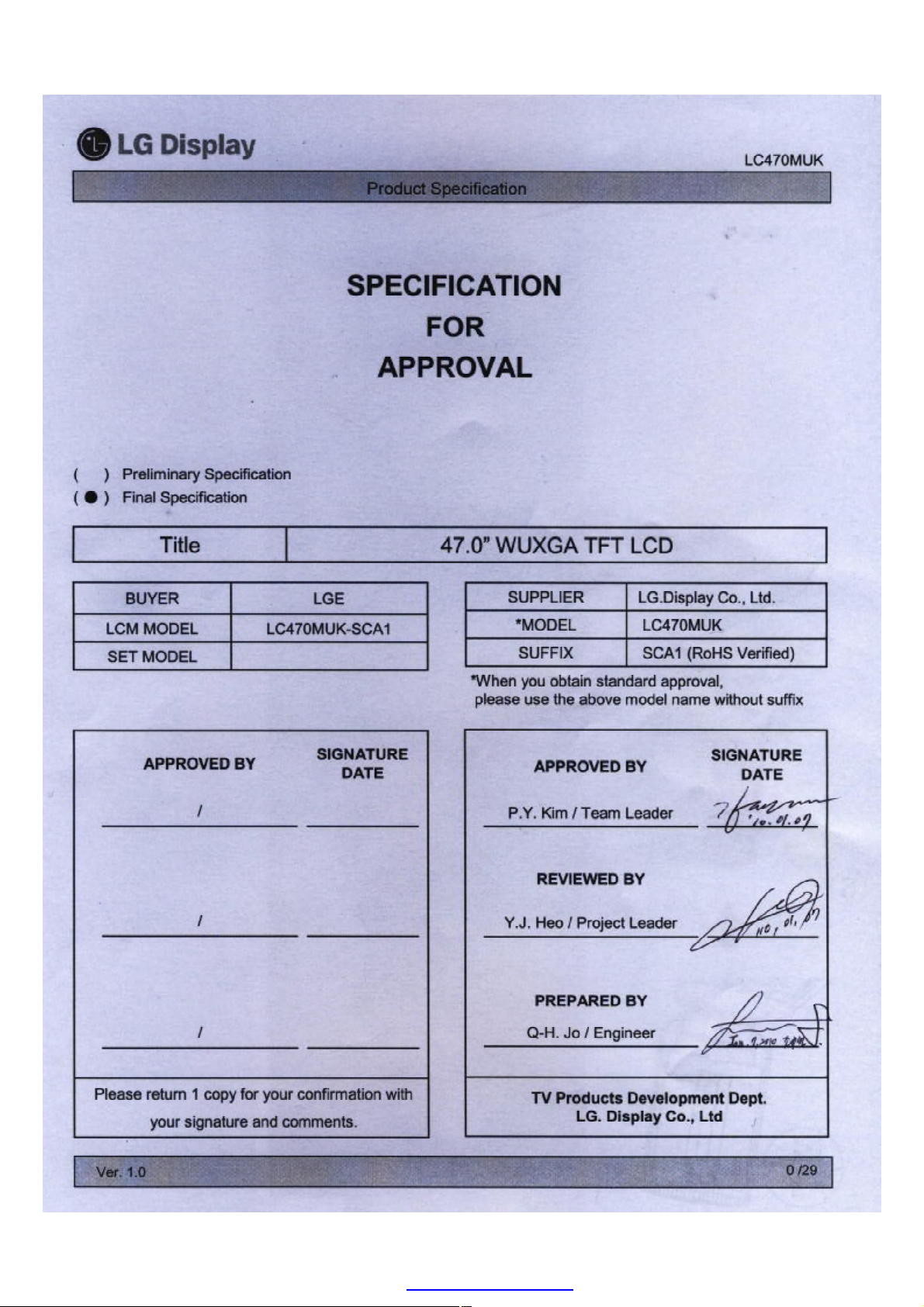
LC470MUK
Product Specification
SPECIFICATION
FOR
APPROVAL
)
(
(
Preliminary Specification
)
Final Specification
●
47.0” WUXGA TFT LCDTitle
SET MODEL
APPROVED BY
LGEBUYER
LC470MUK-SCA1LCM MODEL
*When you obtain standard approval,
please use the above model name without suffix
SIGNATURE
DATE
/
/
/
APPROVED BY
P.Y. Kim / Team Leader
REVIEWED BY
Y.J. Heo/ Project Leader
PREPARED BY
Q-H. Jo / Engineer
LG.Display Co., Ltd.SUPPLIER
LC470MUK*MODEL
SCA1 (RoHS Verified)SUFFIX
SIGNATURE
DATE
Please return 1 copy for your confirmation with
your signature and comments.
Ver. 1.0
TV Products Development Dept.
PDF created with pdfFactory Pro trial version www.pdffactory.com
LG. Display Co., Ltd
0/29
Page 2
Product Specification
CONTENTS
LC470MUK
Number
1
2
3
3-1
3-2
3-3
3-4
3-5
3-6
4
5
CONTENTS
RECORD OF REVISIONS
GENERAL DESCRIPTION
ABSOLUTE MAXIMUM RATINGS
ELECTRICAL SPECIFICATIONS
ELECTRICAL CHARACTERISTICS
INTERFACE CONNECTIONS
SIGNAL TIMING SPECIFICATIONS
DATA MAPPING AND TIMING
PANEL PIXEL STRUCTURE
POWER SEQUENCE
OPTICAL SPECIFICATIONS
MECHANICAL CHARACTERISTICS
ITEM
Page
0COVER
1
2
3
4
5
5
7
9
12
13
14
15
19
6
7
8
8-1
9
Ver. 1.0
7-1
9-1
9-2
9-3
9-4
9-5
RELIABILITY
INTERNATIONAL STANDARDS
ENVIRONMENT
PACKING
PACKING FORM
PRECAUTIONS
ASSEMBLY PRECAUTIONS
OPERATING PRECAUTIONS
ELECTROSTATIC DISCHARGE CONTROL
PRECAUTIONS FOR STRONG LIGHT EXPOSURE
STORAGE
21
22
22
23
23
24
24
24
25
25
25
1/29
PDF created with pdfFactory Pro trial version www.pdffactory.com
Page 3
Product Specification
RECORD OF REVISIONS
DescriptionPageRevision DateRevision No.
Preliminary Specification(First Draft) -Sep. 18, 20090.1
Corrected the ‘MODULE CONNECTOR(CN1) PIN CONFIGURATION’7, 8Sep. 25, 20090.2
Corrected the ‘Last Data Latch to SOE Timing’10
Corrected the ‘ELECTRICAL CHARACTERISTICS’5Nov. 13, 20090.3
Added the ‘APPENDIX-IV’29
Corrected the ‘LCD Connector (CN1) and (CN2)’7,8Nov. 20, 20090.4
Changed the ‘ELECTRICAL CHARACTERISTICS’ and the ‘Note’5Dec. 30, 2009 0.5
LC470MUK
7,8
7,8
Modified the ‘MODULE CONNECTOR(CN1, CN2) PIN
CONFIGURATION’ for normal operation.
Modified the ‘Note’ for ‘MODULE CONNECTOR(CN1, CN2) PIN
CONFIGURATION’
Modified the ‘Note’ for ‘POWER SEQUENCE’14
Added the ‘Color Coordinates’ in ‘Table 6’15
Modified the ‘Common Voltage’5Jan. 7, 20100.6
Final Specification-Jan. 7, 20101.0
Ver. 1.0
PDF created with pdfFactory Pro trial version www.pdffactory.com
2/29
Page 4
LC470MUK
Product Specification
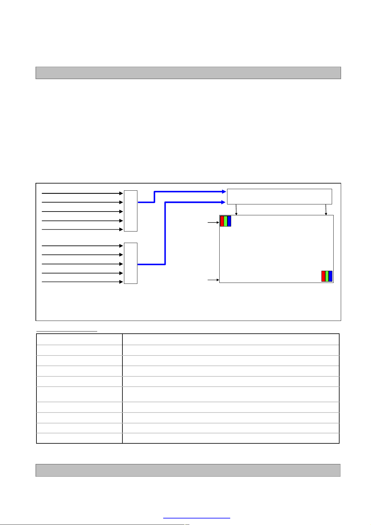
1. General Description
The LC470MUK is a Color Active Matrix Liquid Crystal Display with an integral the Source PCB and Gate
implanted on Panel (GIP). The matrix employs a-Si Thin Film Transistor as the active element.
It is a transmissive type display operating in the normally black mode. It has a 46.96 inch diagonally measured
active display area with WUXGA resolution (1080 vertical by 1920horizontal pixel array).
Each pixel is divided into Red, Green and Blue sub-pixels or dots which are arranged in vertical stripes.
Gray scale or the luminance of the sub-pixel color is determined with a 8-bit gray scale signal for each dot.
Therefore, it can present a palette of more than 16.7M(true) colors.
It is intended to support LCD TV, PCTV where high brightness, super wide viewing angle, high color gamut,
high color depth and fast response time are important.
Power (VCC, VDD, VGH, VGL)
Source Control Signal
Gate Control Signal
Gamma Reference Voltage
mini-LVDS (RGB) for Left drive
CN1
(60pin)
S1 S1920
G1
Source Driver Circuit
Power (VCC, VDD, VGH, VGL)
Source Control Signal
Gate Control Signal
Gamma Reference Voltage
mini-LVDS (RGB) for Right drive
General Features
Drive IC Data Interface
TFT -LCD Panel
(1920 × RGB × 1080 pixels)
CN2
(60pin)
G1080
46.96 inches(1192.78mm) diagonalActive Screen Size
1061.8 (H) x 606.8 (V) x 1.8 (D) mm (Typ.)Outline Dimension
0.5415 mm x 0.5415 mmPixel Pitch
1920 horiz. by 1080 vert. Pixels, RGB stripe arrangementPixel Format
8-bit, 16.7 M colorsColor Depth
Source D-IC : 8-bit mini-LVDS, gamma reference voltage, and control signals
Gate D-IC : Gate In Panel
Viewing angle free ( R/L 178 (Min.), U/D 178 (Min.))Viewing Angle (CR>10)
2.50Kg (Typ.) Weight
Transmissive mode, Normally blackDisplay Mode
Hard coating(3H), Anti-glare treatment (Haze 10%)Surface Treatment (Top)
[Gate In Panel]
Ver. 1.0
PDF created with pdfFactory Pro trial version www.pdffactory.com
3/29
Page 5
LC470MUK
Product Specification
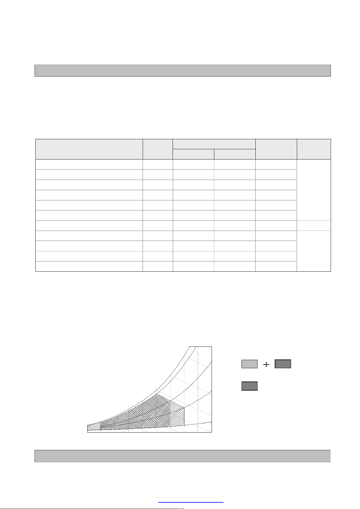
2. Absolute Maximum Ratings
The following items are maximum values which, if exceeded, may cause faulty operation or damage to the
LCD module.
Table 1. ABSOLUTE MAXIMUM RATINGS
Parameter Symbol
Unit Note
Min Max
VDC+4.0-0.5VCCLogic Power Voltage
VDC+30.0+18.0VGHGate High Voltage
VDC-4.0-8.0VGLGate Low Voltage
Source D-IC Analog Voltage VDD -0.3 +18.0 VDC
Gamma Ref. Voltage (Upper) VGMH ½VDD-0.5 VDD+0.5 VDC
Gamma Ref. Voltage (Low) VGML -0.3 ½ VDD+0.5 VDC
Operating Temperature TOP 0 +50 °C
Storage Temperature TST -20 +60 °C
Operating Ambient Humidity HOP 10 90 %RH
Storage Humidity HST 10 90 %RH
Value
Note:
1. Ambient temperature condition (Ta = 25 ± 2 °C )
2. Temperature and relative humidity range are shown in the figure below. Wet bulb temperature
should be Max 39 °C and no condensation of water.
3. Gravity mura can be guaranteed below 40℃ condition.
4. The maximum operating temperature is based on the test condition that the surface temperature
of display area is less than or equal to 68 ℃ with LCD module alone in a temperature controlled
chamber. Thermal management should be considered in final product design to prevent the surface
temperature of display area from being over 68 ℃. The range of operating temperature may
degrade in case of improper thermal management in final product design.
90%
60
60%
1
4°C+68-TSURPanel Front Temperature
2,3
40
50
40%
10%
Wet Bulb
Temperature [°C]
30
20
10
0
10 20 30 40 50 60 70 800-20
Dry Bulb Temperature [°C]
Ver. 1.0
PDF created with pdfFactory Pro trial version www.pdffactory.com
Storage
Operation
Humidity
[(%)RH]
4/29
Page 6
LC470MUK
Product Specification
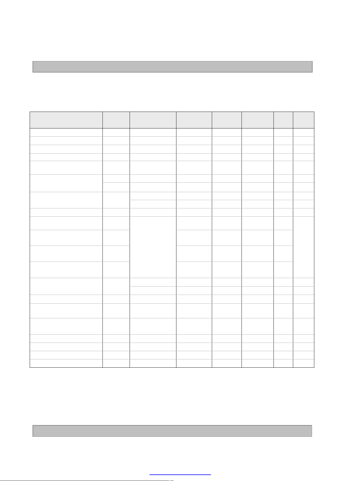
3. Electrical Specifications
3-1. Electrical Characteristics
It requires several power inputs. The VCC is the basic power of LCD Driving power sequence, Which is used
to logic power voltage of Source D-IC and GIP.
Table 2. ELECTRICAL CHARACTERISTICS
Parameter Symbol Condition MIN TYP MAX Unit Note
Logic Power Voltage VCC - 3.0 3.3 3.6 VDC
Logic High Level Input Voltage VIH 2.7 VCC VDC
Logic Low Level Input Voltage VIL 0 0.6 VDC
Source D-IC Analog Voltage VDD - 15.3 15.5 15.7 VDC
Half Source D-IC Analog
Voltage
Gamma Reference Voltage
Mini-LVDS Clock frequency CLK 3.0V≤VCC ≤3.6V 312 MHz
mini-LVDS input Voltage
(Center)
mini-LVDS input Voltage
Distortion (Center)
mini-LVDS differential
Voltage range
mini-LVDS differential
Voltage range Dip
Gate Low Voltage VGL -5.2 -5.0 -4.8 VDC
GIP Bi-Scan Voltage
GIP Refresh Voltage
GIP Start Pulse Voltage VST - VGL - VGH V
GIP Operating Clock GCLK - VGL - VGH V
Total Power Current
Total Power Consumption
H_VDD - 7.45 7.68 7.82 VDC 7
V
GMH
V
GML
VcomCommon Voltage
VIB
ΔVIB 0.8 V
VID 150 800 mV
ΔVID 25 800 mV
VGHGate High Voltage
VGI_P
VGI_N
VGH
even/odd
ILCD - 800 1040 mA 2
PLCD - 8.53 11.09 Watt 2
(GMA1 ~ GMA9) ½*VDD VDD-0.2
(GMA10 ~ GMA18) 0.2 ½*VDD
Reverse 6.47 6.77 7.07 V
0.7 + (VID/2)
Mini-LVDS Clock
and Data
@ 0℃ 28.7 29 29.3 VDC
- VGL - VGH VDC
- VGL - VGH V
(VCC-1.2)
− VID / 2
V7.076.776.47Normal
V
VDC28.32827.7@ 25℃
5
Note:
1. The specified current and power consumption are under the VLCD=12V., 25 ± 2°C, fV=120Hz
condition whereas mosaic pattern(8 x 6) is displayed and fVis the frame frequency.
2. The above spec is based on the basic model.
3. All of the typical gate voltage should be controlled within 1% voltage level
4. Ripple voltage level is recommended under 10%
5. In case of mini-LVDS signal spec, refer to Fig 2 for the more detail.
6. Logic Level Input Signal : SOE,POL,GSP,H_CONV,OPT_N
7. HVDD Voltage level is half of VDD and it should be between Gamma9 and Gamma10.
Ver. 1.0
PDF created with pdfFactory Pro trial version www.pdffactory.com
5/29
Page 7

VCM (0V)
LC470MUK
Product Specification
VGH
VGHM
GND
VGL
Without GPM With GPM
FIG. 1 Gate Output Wave form without GPM and with GPM
VID
△VID
△VIB
VIB
VID
* Differential Probe
△VID
* Active Probe
FIG. 2 Description of VID, ΔVIB, ΔVID
* Source PCB
FIG. 3 Measure point
Ver. 1.0
PDF created with pdfFactory Pro trial version www.pdffactory.com
6/29
Page 8
LC470MUK
Product Specification
3-2. Interface Connections
This LCD panel employs two kinds of interface connection, two 60-pin FFC connector are used for the
module electronics.
3-2-1. LCD Module
-LCD Connector (CN1): TF06L-60S-0.5SH (Manufactured by HRS) or Equivalent
Table 4-1. MODULE CONNECTOR(CN1) PIN CONFIGURATION
DescriptionSymbolNoDescriptionSymbolNo
10
11
12
13
14
15
16
17
18
19
20
21
22
23
24
25
26
27
28
29
30
1
LTD OUTPUTLTD_OUT2
3
4
5
6
7
8
9
48GroundGND
49Driver Power Supply VoltageVDD
50Driver Power Supply VoltageVDD
51Half Driver Power Supply VoltageH_VDD
52Half Driver Power Supply VoltageH_VDD
53GroundGND
54Logic Power Supply VoltageVCC
55Logic Power Supply VoltageVCC
56GroundGND
57Left Mini LVDS Receiver Signal(5-) LLV5 58Left Mini LVDS Receiver Signal(5+) LLV5 +
59Left Mini LVDS Receiver Signal(4-) LLV4 -
Left Mini LVDS Receiver Signal(3-) LLV3 -31GroundGND
Left Mini LVDS Receiver Signal(3+) LLV3 +32
Left Mini LVDS Receiver Clock Signal(-) LCLK -33GIP GATE Clock 1GCLK1
Left Mini LVDS Receiver Clock Signal(+) LCLK +34GIP GATE Clock 2GCLK2
Left Mini LVDS Receiver Signal(2-) LLV2 -35GIP GATE Clock 3GCLK3
Left Mini LVDS Receiver Signal(2+) LLV2 +36GIP GATE Clock 4GCLK4
Left Mini LVDS Receiver Signal(1-) LLV1 -37GIP GATE Clock 5GCLK5
Left Mini LVDS Receiver Signal(1+) LLV1 +38GIP GATE Clock 6GCLK6
Left Mini LVDS Receiver Signal(0-) LLV0 -39GIP Bi-Scan (Normal =VGL Rotate = VGH)VGI_N
Left Mini LVDS Receiver Signal(0+) LLV0 +40GIP Bi-Scan (Normal =VGH Rotate = VGL)VGI_P
GroundGND41GIP Panel VDD for Odd GATE TFTVGH_ODD
Source Output Enable SIGNALSOE42GIP Panel VDD for Even GATE TFTVGH_EVEN
Polarity Control SignalPOL43GATE Low VoltageVGL
GATE Start PulseGSP44VERTICAL START PULSEVST
"H“ H 2dot Inversion/ "L" H 1dot InversionH_CONV45GroundGND
“H” Normal Display / “L” Rotation DisplayOPT_N46VCOM Left Feed-Back OutputVCOM_L_FB
GroundGND47VCOM Left InputVCOM_L
GAMMA VOLTAGE 18 (Output From LCD)GMA 18
GAMMA VOLTAGE 16GMA 16
GAMMA VOLTAGE 15GMA 15
GAMMA VOLTAGE 14GMA 14
GAMMA VOLTAGE 12GMA 12
GAMMA VOLTAGE 10 (Output From LCD)GMA 10
GAMMA VOLTAGE 9 (Output From LCD)GMA 9
GAMMA VOLTAGE 7GMA 7
GAMMA VOLTAGE 5GMA 5
GAMMA VOLTAGE 4GMA 4
GAMMA VOLTAGE 3GMA 3
GAMMA VOLTAGE 1 (Output From LCD)GMA 1
GroundGND60Left Mini LVDS Receiver Signal(4+) LLV4 +
Note :
1. Pleaserefer to application note for details.
(GIP & Half VDD & Gamma Voltage & H_CONV setting)
2. These 'input signal' (OPT_N,H_CONV) should be connected.
Ver. 1.0
PDF created with pdfFactory Pro trial version www.pdffactory.com
7/29
Page 9

Product Specification
-LCD Connector (CN2):TF06L-60S-0.5SH(Manufactured by HRS) or Equivalent
Table 4-2. MODULE CONNECTOR(CN2) PIN CONFIGURATION
LC470MUK
DescriptionSymbolNoDescriptionSymbolNo
14
15
16
17
18
19
20
21
22
23
24
25
26
27
28
29
30
1
GAMMA VOLTAGE 1 (Output From LCD)GMA 12
GAMMA VOLTAGE 3GMA 33
GAMMA VOLTAGE 4GMA 44
GAMMA VOLTAGE 5GMA 55
GAMMA VOLTAGE 7GMA 76
GAMMA VOLTAGE 9 (Output From LCD)GMA 97
GAMMA VOLTAGE 10 (Output From LCD)GMA 108
GAMMA VOLTAGE 12GMA 129
GAMMA VOLTAGE 14GMA 1410
GAMMA VOLTAGE 15GMA 1511
GAMMA VOLTAGE 16GMA 1612
GAMMA VOLTAGE 18 (Output From LCD)GMA 1813
59Right Mini LVDS Receiver Signal(2-) RLV2 -
Right Mini LVDS Receiver Signal(1-) RLV1 -31GroundGND
Right Mini LVDS Receiver Signal(1+) RLV1 +32
Right Mini LVDS Receiver Signal(0-) RLV0 -33
Right Mini LVDS Receiver Signal(0+) RLV0 +34
GroundGND35
Logic Power Supply VoltageVCC36
Logic Power Supply VoltageVCC37
GroundGND38
Half Driver Power Supply VoltageH_VDD39
Half Driver Power Supply VoltageH_VDD40
Driver Power Supply VoltageVDD41
Driver Power Supply VoltageVDD42
GroundGND43
VCOM Right InputVCOM_R44GroundGND
VCOM Right Feed-Back OutputVCOM_R_FB45“H” Normal Display / “L” Rotation DisplayOPT_N
GroundGND46"H“ H 2dot Inversion/ "L" H 1dot InversionH_CONV
VERTICAL START PULSEVST47GATE Start PulseGSP
GATE Low VoltageVGL48Polarity Control SignalPOL
GIP Panel VDD for Even GATE TFTVGH_EVEN49Source Output Enable SIGNALSOE
GIP Panel VDD for Odd GATE TFTVGH_ODD50GroundGND
GIP Bi-Scan (Normal =VGH Rotate = VGL)VGI_P51Right Mini LVDS Receiver Signal(5-) RLV5 GIP Bi-Scan (Normal =VGL Rotate = VGH)VGI_N52Right Mini LVDS Receiver Signal(5+) RLV5 +
GIP GATE Clock 6GCLK653Right Mini LVDS Receiver Signal(4-) RLV4 GIP GATE Clock 5GCLK554Right Mini LVDS Receiver Signal(4+) RLV4 +
GIP GATE Clock 4GCLK455Right Mini LVDS Receiver Signal(3-) RLV3 GIP GATE Clock 3GCLK356Right Mini LVDS Receiver Signal(3+) RLV3 +
GIP GATE Clock 2GCLK257Right Mini LVDS Receiver Clock Signal(-) LCLK GIP GATE Clock 1GCLK158Right Mini LVDS Receiver Clock Signal(+) LCLK +
LTD OUTPUTLTD_OUT
GroundGND60Right Mini LVDS Receiver Signal(2+) RLV2 +
Note :
1. Pleaserefer to application note for details.
(GIP & Half VDD & Gamma Voltage & H_CONV setting)
2. These 'input signal' (OPT_N,H_CONV) should be connected.
CN 2
CN 1
Source Right PCB
#1 #60
Ver. 1.0
#1 #60
PDF created with pdfFactory Pro trial version www.pdffactory.com
Source Left PCB
8/29
Page 10

3-3. Signal Timing Specifications
Table 6. Timing Requirements
Parameter Symbol Condition Min Typ Max Unit Note
LC470MUK
Product Specification
Mini Clock pulse period
Mini Clock pulse low period
Mini Clock pulse high period
Mini Data setup time
Mini Data hold time
Reset low to SOE rising time
SOE to Reset input time
Receiver off to SOE timing
POL signal to SOE setup time
POL signal to SOE hold time
Reset High Period
SOE signal GSP setup time
SOE signal GSP Hold time
SOE signal Pulse Width
Note :
1. Mini-LVDS timing measure conditions
: 268MHz < Clock Frequency < 312MHz , 150mV < VID < 800mV @ 3.0<VCC<3.3
2. Setup time and hold time couldn’t be satisfied at the same time
T1
T2
T3
T6
T7
T8
T9
T10
T11
T12
T13
T14
T15
T16
3.2 3.4 ns
1.6 - - ns
1.6 - - ns
0.6 - - ns
0.6 - - ns
0 - - ns
200 - - ns
10 - -
-5 - - ns
6 - - ns
3
100 ns
100 ns
200 ns
CLK
cycle
CLK
cycle
1
T1
70%
T7
T2
70%
30%
30%
T5
30%
CLK-
CLK+
LV0+, -
to
LV5+,-
T6 T7
50%
T3
T6
T5
FIG 4. Source D-IC Input Data Latch Timing Waveform
Ver. 1.0
PDF created with pdfFactory Pro trial version www.pdffactory.com
T4
30%
70%
VDIFF
T4
70%
VDIFF
9/29
Page 11

Product Specification
LC470MUK
CLK+
LV0+,LV1+,-
to
LV5+,-
SOE
Read The Reset=H
Read The Reset=L 1stDATA
T1
T2
T3
NA
R=H R=H R=H NAR=L R=L NA D D DR=L DD
T13
NA
T8
70%
30%
NA NA NA NANA NA NA D D DNA DD
T9
FIG 5-1. Input Data Timing for 1stSource D-IC Chip
Last DATA
Ver. 1.0
CLK+
LV0+,-
LV1+,-
to
LV5+,-
SOE
(640)
D D D
D D D
(641)
NA NA NA NA NA R=LNA R=L R=L
NA NA NA NA NA NANA NA NA
T10
FIG 5-2. Last Data Latch to SOE Timing
T8
70%
30%
10/29
PDF created with pdfFactory Pro trial version www.pdffactory.com
Page 12

Product Specification
LC470MUK
SOE
POL
GSP
GSP
70%
T16
T14
T11
70%
30%
30%
70%
T15
T12
70%
30%
70%
30%
70%
Ver. 1.0
SOE
1stline data 1stline output
FIG 6. POL, GSP and SOE Timing Waveform
11/29
PDF created with pdfFactory Pro trial version www.pdffactory.com
Page 13

Product Specification
3-4. Data Mapping and Timing
Display data and control signal (RESET) are input to LV0 to LV5.
3-4-1. Control signal input mode
CLK +
LC470MUK
LV0 +
RESET RESET RESET RESET RESET RESET RESET RESET RESET RESET
3-4-2. Display data input mode
CLK+
LV0+
LV1+
LV2+
LV3+
LV4+
LV5+
Note :
1. For data mapping, please refer to panel pixel structure Fig.8
D01 D02 D03 D04 D05 D06D00
D11 D12 D13 D14 D15 D16D10 D17
D21 D22 D23 D24 D25 D26D20 D27
D31 D32 D33 D34 D35 D36D30 D37
D41 D42 D43 D44 D45 D46D40 D47
D51 D52 D53 D54 D55 D56D50 D57
DATA INPUT CYCLE
D07 D00
Fig. 7 Mini-LVDS Data
D10
D20
D30
D40
D50
Ver. 1.0
PDF created with pdfFactory Pro trial version www.pdffactory.com
12/29
Page 14

3-5. Panel Pixel Structure
D1 D2 D3 D4 D5 D1918 D1919 D1920 D1921
G1
G2
G3
G4
G5
G6
LC470MUK
Product Specification
G1078
G1079
G1080
FIG. 8 Panel Pixel Structure
Ver. 1.0
PDF created with pdfFactory Pro trial version www.pdffactory.com
13/29
Page 15

3-6. Power Sequence
3-6-1. LCD Driving circuit
Power Supply For LCD VCC
Power Supply For LCD
VDD, HVDD,VGH, Gamma Ref.
Voltage
Power Supply For LCD
VGL
0V
0V
Product Specification
70%
50%
100%
T1
T2
VGH
90%
LC470MUK
T7
GIP Signal For LCD
Power For LED
Table 7. POWER SEQUENCE
Parameter
T1 0.5 - ms
T3 0
T4 10
T5 0 - ms
Note : 1. Power sequence for Source D-IC must follow the Case1 & 2.
※ Please refer to Appendix V for more details.
2. VGH Odd signal should be started “High” status and VGH even & odd can not be “High at the
same time.
3. Power Off Sequence order is reverse of Power OnCondition including Source D-IC.
4. GCLK On/Off Sequence
Normal : GCLK4 à GCLK5 à GCLK6 à GCLK1 à GCLK2 à GCLK3.
Reverse : GCLK3 à GCLK2 àGCLK1 àGCLK6 à GCLK5 à GCLK4.
5. VDD_odd/even transition time should be within V_blank
Ver. 1.0
VGH
even/Odd
VST
GCLK1~6
Value
Min Typ Max
0.5T2
T3
T4
..
..
T5
T6
Ta= 25±2°C, fV=120Hz, Dclk=74.25MHz
-
-
-
..
T6’
LED on
Unit Notes
ms
ms
ms 2
ms-20T6 / T6’
sec-2T7
14/29
PDF created with pdfFactory Pro trial version www.pdffactory.com
Page 16

LC470MUK
Product Specification
4. Optical Specification
Optical characteristics are determined after the unit has been ‘ON’ and stablein a dark environmentat
25±2°C. The values are specified at an approximate distance 50cm fromthe LCD surface at a viewing angle
of Φand θ equal to 0 °.
It is presented additional information concerning the measurement equipment and method in FIG. 9.
Optical Stage(x,y)
LCD Module
FIG. 9 Optical Characteristic Measurement Equipment and Method
Table 6. OPTICAL CHARACTERISTICS
SymbolParameter
Contrast Ratio
Response Time
50cm
Pritchard 880 or
equivalent
Ta= 25±2°C, VDD,H_VDD,VGH,VGL=typ,
fV=120Hz, Dclk=74.25MHz,
EXTVBR-B =100% Back Light : LGD B/L
Value
MaxTypMin
-TrRising
-TfFalling
128
1410
NoteUnit
1-14001000CR
4ms
Color Coordinates
[CIE1931]
Viewing Angle (CR>10)
x axis, right(φ=0°)
x axis, left (φ=180°)
y axis, up (φ=90°)
y axis, down (φ=270°)
Ver. 1.0
RED
GREEN
BLUE
Rx
Ry
Gx
Gy
Bx
By
Typ
-0.03
0.649
0.332
0.307
0.595
0.149
0.059
Typ
+0.03
--89θr
--89θl
--89θu
--89θd
5degree
6---Gray Scale
15/29
PDF created with pdfFactory Pro trial version www.pdffactory.com
Page 17

Product Specification
Note :
1. Contrast Ratio(CR) is defined mathematically as :
LC470MUK
Contrast Ratio =
Surface Luminance with all white pixels
Surface Luminance with all black pixels
It is measured at center 1-point.
2. Response time is the time required for the display to transition from G(0) to G(255) (Rise Time, TrR)
and from G(0) to G(255) (Decay Time, TrD). For additional information see the FIG. 11.
3. Viewing angle is the angle at which the contrast ratio is greater than 10. The angles are
determined for the horizontal or x axis and the vertical or y axis with respect to the z axis which
is normal to the LCD module surface. For more information, seethe FIG. 12.
4. Gray scale specification
Gamma Value is approximately 2.2. For more information, see the Table 7.
Table 7. GRAY SCALE SPECIFICATION
Gray Level
Ver. 1.0
L0
L15
L31
L47
L63
L79
L95
L111
L127
L143
L159
L175
L191
L207
L223
L239
L255
Luminance [%] (Typ)
0.07
0.27
1.04
2.49
4.68
7.66
11.5
16.1
21.6
28.1
35.4
43.7
53.0
63.2
74.5
86.7
100
Positive
Voltage
Negative
Voltage
Gray Level
L0
L1
L31
L63
L127
L191
L223
L255
L255
L223
L191
L127
L63
L31
L1
L0
Gamma Ref.
Gamma9
Gamma8
Gamma7
Gamma6
Gamma5
Gamma4
Gamma3
Gamma1
Gamma18
Gamma16
Gamma15
Gamma14
Gamma13
Gamma12
Gamma11
Gamma10
16/29
PDF created with pdfFactory Pro trial version www.pdffactory.com
Page 18

Product Specification
Measuring point for surface luminance & luminance variation
H
A
LC470MUK
③②
V
①
B
A : H / 4 mm
④
FIG. 10 5 Points for Luminance Measure
Response time is defined as the following figure and shall be measured by switching the input signal for
“Gray(N)” and “Gray(M)”.
TrR
100
90
⑤
TrD
B : V / 4 mm
@ H,V : Active Area
Optical
Response
Ver. 1.0
10
0
Gray(N)
N,M = Black~White, N<M
FIG. 11 Response Time
Gray(M)
PDF created with pdfFactory Pro trial version www.pdffactory.com
Gray(N)
17/29
Page 19

Dimension of viewing angle range
LC470MUK
Product Specification
φ
= 180°, Left
φ
= 270°, Down
Normal
θ
φ
FIG.12 Viewing Angle
E
Y
φ
= 90°, Up
φ
= 0°, Right
Ver. 1.0
PDF created with pdfFactory Pro trial version www.pdffactory.com
18/29
Page 20

Product Specification
5. Mechanical Characteristics
Table 8 provides general mechanical characteristics.
Table 8. MECHANICAL CHARACTERISTICS
LC470MUK
ValueItem
1061.8 mmHorizontal
Outline Dimension
Active Display Area
Surface Treatment
2.50 Kg (Typ.) , 2.75 Kg (Max.) Weight
Hard coating(3H)
Anti-glare treatment of the front polarizer(10%)
606.8 mmVertical
1.8 mmDepth
1039.68 mmHorizontal
584.82 mmVertical
Note : Please refer to a mechanical drawing in terms of tolerance at the next page.
Ver. 1.0
PDF created with pdfFactory Pro trial version www.pdffactory.com
19/29
Page 21

[ FRONT VIEW ]
LC470MUK
Product Specification
Ver. 1.0
PDF created with pdfFactory Pro trial version www.pdffactory.com
20/29
Page 22

Product Specification
6. Reliability
Table 9. ENVIRONMENT TEST CONDITION
LC470MUK
ConditionTest ItemNo.
Ta= 60°C 240hHigh temperature storage test1
Ta= -20°C 240hLow temperature storage test2
Ta= 50°C 50%RH 240hHigh temperature operation test3
Ta= 0°C 240hLow temperature operation test4
Ta= 40 °C ,90%RHHumidity condition Operation5
6
Altitude operating
storage / shipment
0 -15,000 ft
0 -40,000 ft
Note : Before and after Reliability test, Board ass’y should be operated with normal function.
Ver. 1.0
PDF created with pdfFactory Pro trial version www.pdffactory.com
21/29
Page 23

Product Specification
7. International Standards
7-1. Environment
a) RoHS, Directive 2002/95/EC of the European Parliament and of thecouncil of 27 January 2003
LC470MUK
Ver. 1.0
PDF created with pdfFactory Pro trial version www.pdffactory.com
22/29
Page 24

Product Specification
8. Packing
8-1. Packing Form
a) Package quantity in one Pallet : 70 pcs
b) Pallet Size : 1250 mm(L) X 800 mm(W) X 1105 mm(H)
LC470MUK
Ver. 1.0
PDF created with pdfFactory Pro trial version www.pdffactory.com
23/29
Page 25

LC470MUK
Product Specification
9. Precautions
Please pay attention to the followings when you use this TFT LCDpanel.
9-1. Assembly Precautions
(1) Please attach the surface transparent protective plate to the surface in order to protect the polarizer.
Transparent protective plate should have sufficient strength in order to the resist external force.
(2) You should adopt radiation structure to satisfy the temperature specification.
(3) Acetic acid type and chlorine type materials for the cover case are not desirable because the former
generates corrosive gas of attacking the polarizer at high temperature and the latter causes circuit break
by electro-chemical reaction.
(4) Do not touch, push or rub the exposed polarizers with glass,tweezers or anything harder than HB
pencil lead. And please do not rub with dust clothes with chemical treatment.
Do not touch the surface of polarizer for bare hand or greasy cloth.(Some cosmetics are detrimental
to the polarizer.)
(5) When the surface becomes dusty, please wipe gently with absorbent cotton or other soft materials like
chamois soaks with petroleum benzine. Normal-hexane is recommended for cleaning the adhesives
used to attach front / rear polarizers. Do not use acetone, toluene and alcohol because they cause
chemical damage to the polarizer
(6) Wipe off saliva or water drops as soon as possible. Their long time contact with polarizer causes
deformations and color fading.
(7) Board ass’y should be put on the mold frame properly.
(8) FFC Cable should be connected between System board and Source PCB correctly.
(9) Mechanical structure for backlight system should be designedfor sustaining board ass’y safely.
9-2. Operating Precautions
(1) The spike noise causes the mis-operation of circuits. It should be lower than following voltage:
V=±200mV(Over and under shoot voltage)
(2) Response time depends on the temperature.(In lower temperature, it becomes longer.)
(3) Brightness depends on the temperature. (In lower temperature, it becomes lower.)
And in lower temperature, response time(required time that brightness is stable after turned on)
becomes longer
(4) Be careful for condensation at sudden temperature change.Condensation makes damage to polarizer or
electrical contacted parts. And after fading condensation, smear or spot will occur.
(5) When fixed patterns are displayed for a long time, remnantimage is likely to occur.
(6) Module has high frequency circuits. Sufficient suppressionto the electromagnetic interference shall be
done by system manufacturers. Grounding and shielding methods may be important to minimized the
interference.
(7) Please do not give any mechanical and/or electrical impactto board assy. Otherwise, it can’t be operated
its full characteristics perfectly.
Ver. 1.0
24/29
PDF created with pdfFactory Pro trial version www.pdffactory.com
Page 26

LC470MUK
Product Specification
9-3. Electrostatic Discharge Control
Since a module is composed of electronic circuits, it is not strong to electrostatic discharge. Make certain that
treatment persons are connected to ground through wrist band etc. And don’t touch interface pin directly.
Panel ground path should be connected to metal ground.
9-4. Precautions for Strong Light Exposure
Strong light exposure causes degradation of polarizer and color filter.
9-5. Storage
When storing the board ass’y as spares for a long time, the following precautions are necessary.
(1) Store them in a dark place. Do not expose the board ass’y to sunlight or fluorescent light. Keep the
temperature between 5°C and 35°C at normal humidity.
(2) The polarizer surface should not come in contact with any other object.
It is recommended that they be stored in the container in which they were shipped.
Ver. 1.0
PDF created with pdfFactory Pro trial version www.pdffactory.com
25/29
Page 27

# APPENDIX-I
■ LC470MUK-SCA1-Pallet Ass’y
LC470MUK
Product Specification
No. Description Material
ⓐ
ⓑ
ⓒ
ⓓ
ⓔ
ⓕ
ⓖ
ⓗ
ⓘ
Ver. 1.0
PDF created with pdfFactory Pro trial version www.pdffactory.com
Pallet Plywood
Carton Plate Single Wall
PE Sheet Carbon
Top Packing EPP
Bottom Packing EPP
Angle Packing Single Wall
Tape OPP
Band PP
Clip Steel
26/29
Page 28

Product Specification
# APPENDIX-II
■ LC470MUK-SCA1-Serial Label
LC470MUK
Model
Serial No.
Work Other
LC470MUK-SCA1
XXXX
Ver. 1.0
PDF created with pdfFactory Pro trial version www.pdffactory.com
27/29
Page 29

# APPENDIX-III
■ LC470MUK-SCA1-Pallet Label
LC470MUK
SCA1
LC470MUK
Product Specification
10 PCS
MADE IN KOREA
001/01-01
XXXXXXXXXXXXX XXX
RoHSVerified
Ver. 1.0
PDF created with pdfFactory Pro trial version www.pdffactory.com
28/29
Page 30

Product Specification
# APPENDIX-IV
■ LC470MUK-SCA1-Source D-IC Power Sequence
LC470MUK
-Input Signal : SOE,POL,GSP,H_CONV,OPT_N
Ver. 1.0
PDF created with pdfFactory Pro trial version www.pdffactory.com
29/29
 Loading...