

LG PFM42V1, PFM-42V1E Schematic

STANDBY
ON
COLOR MONIT OR
SER VICE MANUAL
CAUTION
BEFORE SERVICING THE UNIT,
READ THE SAFETY PRECAUTIONS IN THIS MANUAL.
CHASSIS NO. : CL-50
MODEL: PFM42V1, PFM42V1A, PFM-42V1E
1. PDP CHARACTERISTICS
Type : WVGA Module
Size : 42 inch
Display area :
920.1 (H) x 518.4 (V)
±0.5mm
Cell Pitch :
396um (H) x 1080um (V)
(stand for Green Cell)
Number of gradations :
256 steps for RGB
Peak Brightness : Typ.1000 cd/㎡(1/25white window)
Electrical Interface : LVDS
Contrast Ratio :
Typ.
1000:1(In dark room with 1/25 white)
Power Consumption : Typ.230W(Full White Pattern)
2. OPTICAL CHARACTERISTICS
2-1. White Peak Brightness: 297.5Min(cd/㎡)
(1/25 White window with 40% scren filter RGB mode)
2-2. White Average Brightness: 60Min(Full White window)
3. ENGINEERING SPEC
3-1. Sync Signal
• Type : Composite Video, Y/C,
Component(Y/Cb/Cr),
Hivision(Y/Pb/Pr), Analog RGB,
DVI-D(TMDS)
3-2. Video Input Signal
1)
Composite Video
: 75 Ω terminated(Auto)
NTSC 3.58, PAL 4.43,
SECAM, NTSC4.43, PAL60, PAL-N
PAL-M: 1Vp-p
2) Y/C : 75 Ω terminated
Y: 1Vp-p, Minus Sync
C:
0.286Vp-p(NTSC)/0.3Vp-p(PAL)
3) Component : 75 Ω terminated
(Y/Cb/Cr) NTSC:
0.714Vp-p
/PAL:
0.7Vp-p
SYNC_ON Y:
0.286Vp-p(NTSC)
0.3Vp-p(PAL)
4) Hivision : 75 Ω terminated
(Y/Pb/Pr) Y:
1Vp-p
, Trilevel Sync
Pb, Pr: 0.7Vp-p
5) Analog RGB : 75 Ω terminated
(fH=15~96kHz, fV=48~85Hz)
R/G/B: 0.7Vp-p
SYNC: H/V Separate 1-5Vp-p,
High Impedance,
H/V Composite
: 1-5Vp-p,
High Impedance,
SYNC_ON_GREEN 0.286Vp-p
6) DVI-D : TMDS
3-3. Operating Frequency
Horizontal : 15 ~ 96kHz (ANALOG)
Horizontal : 28 ~ 81kHz (DIGITAL)
Vertical : 48 ~ 85Hz
5. POWER SUPPLY
5-1. Power
: AC 100-240V
±5V
, 50/60Hz
±2%
5-2. Power Consumption
6. ENVIRONMENT
6-1. Operating Temperature: 0°C~+35°C (32°F~95°F)
6-2. Relative Humidity : 20%~90%
(No dew condensation)
6-3. Altitude :~2,000m
7. DIMENSIONS
Width : 1,033 mm (40.67'')
Depth : 102 mm (4.01')
Height : 631 mm (24.84'')
8. WEIGHT
Net. Weight : 27.6kg (60.86 lbs)
Gross Weight : 36.2kg (79.81 lbs)
CONTENTS
SPECIFICATIONS
- 2 -
SPECIFICATIONS ................................................... 2
PRECAUTIONS ....................................................... 3
TIMING CHART ....................................................... 4
OPERATING INSTRUCTIONS ................................ 6
BLOCK DIAGRAM ................................................... 8
DESCRIPTION OF BLOCK DIAGRAM.................... 9
ADJUSTMENT .......................................................12
TROUBLESHOOTING GUIDE .............................. 13
WIRING DIAGRAM ................................................26
SCREW PART LIST................................................ 27
EXPLODED VIEW...................................................29
REPLACEMENT PARTS LIST ...............................31
PIN CONFIGURATION ...........................................45
SCHEMATIC DIAGRAM......................................... 48
MODE
NORMAL
Stand By
AC OFF
Wattage
350 W
3 W
0W
LED COLOR
GREEN
RED
OFF
VIDEO
YES
NO
NO

- 3 -
PRECAUTION
WARNING FOR THE SAFETY-RELATED COMPONENT.
• There are some special components used in LCD
monitor that are important for safety. These parts are
marked on the schematic diagram and the
replacement parts list. It is essential that these critical
parts should be replaced with the manufacturer’s
specified parts to prevent electric shock, fire or other
hazard.
• Do not modify original design without obtaining written
permission from manufacturer or you will void the
original parts and labor guarantee.
TAKE CARE DURING HANDLING THE LCD MODULE
WITH BACKLIGHT UNIT.
• Must mount the module using mounting holes arranged
in four corners.
• Do not press on the panel, edge of the frame strongly
or electric shock as this will result in damage to the
screen.
• Do not scratch or press on the panel with any sharp
objects, such as pencil or pen as this may result in
damage to the panel.
• Protect the module from the ESD as it may damage the
electronic circuit (C-MOS).
• Make certain that treatment person’s body are
grounded through wrist band.
• Do not leave the module in high temperature and in
areas of high humidity for a long time.
• The module not be exposed to the direct sunlight.
• Avoid contact with water as it may a short circuit within
the module.
• If the surface of panel become dirty, please wipe it off
with a softmaterial. (Cleaning with a dirty or rough cloth
may damage the panel.)
WARNING
BE CAREFUL ELECTRIC SHOCK !
• If you want to replace with the new backlight (CCFL) or
inverter circuit, must disconnect the AC adapter
because high voltage appears at inverter circuit about
650Vrms.
• Handle with care wires or connectors of the inverter
circuit. If the wires are pressed cause short and may
burn or take fire.
CAUTION
Please use only a plastic screwdriver to protect yourself
from shock hazard during service operation.
- 4 -
Mode
H/V
Sort
1
2
3
4
5
6
7
8
9
10
11
12
13
14
15
640 x 350
H – 31.500 900 720 180 72 90 18
V – 66.667Hz 525 480 45 3 39 3
640 x 480
H – 31.500 900 720 180 72 90 18
V + 70.156Hz 449 400 49 3 34 12
640 x 480
(MAC13”)
H + 31.469 800 640 160 96 56 8
V – 70.086Hz 449 350 99 2 66 31
720 x 400
(TEXT)
H + 37.879 1056 800 256 128 88 40
V + 60.317Hz 628 600 28 4 23 1
800 x 600
H – 49.731 1152 832 320 64 224 32
V – 74.559Hz 667 624 43 3 37 3
832 x 624
(MAC16”)
H – 48.363 1344 1024 320 136 160 24
V – 60.004Hz 806 768 38 6 29 3
1024x768
H + 60.023 1312 1024 288 96 176 16
V + 75.029Hz 800 768 32 3 28 1
1024x768
H + 68.677 1376 1024 352 96 208 48
V + 84.997Hz 808 768 40 3 36 1
1024x768
H + 67.500 1600 1152 448 128 256 64
V + 75.000Hz 900 864 36 3 32 1
1152x864
H – 68.681 1456 1152 304 128 144 32
V – 75.062Hz 915 870 45 3 39 3
1280 x 960
1152x870
(MAC21”)
H + 63.981 1688 1280 408 112 248 48
V + 60.020Hz 1066 1024 42 3 38 1
H + 60.000 1800 1280 520 112 312 96
V + 60.000Hz 1000 960 40 3 36 1
1280x1024
H – 74.537 2160 1600 560 168 280 112
V + 59.869Hz 1245 1200 45 4 38 3
1600x1200
H + 31.020 1088 848 240 112 112 16
V + 60.000Hz 517 480 37 8 23 6
848x480
Sync
Polarity
Frequency
Dot
Clock
Back Porch
(F)
Front Porch
(C)
Resolution
25.175
25.175
30.240
28.350
40.000
57.290
65.000
78.750
94.500
108.000
100.000
108.000
108.000
161.000
33.750
<< Dot Clock (MHz), Horizontal Frequency (kHz), Vertical Frequency (Hz), Horizontal etc... (µs), Vertical etc... (ms) >>
H – 31.469 800 640 160 96 48 16
V – 59.940Hz 525 480 45 2 33 10
Sync Duration
(D)
Blanking time
(B)
Video Active Time
(A)
Total Period
(E)
TIMING CHART
VIDEO
SYNC
C
D
C
F
A
B
1. PC MODE & COMPOSITE MODE
- 5 -
Mode
H/V
Sort
16
17
18
19
20
21
22
23
24
848x480
H – 37.684 1088 848 240 80 120 40
V + 74.769Hz 504 480 24 5 16 3
848x480
H – 47.776 1664 1280 384 128 192 64
V + 59.870Hz 798 768 30 7 20 3
848x480
H – 29.830 1056 848 208 80 104 24
V + 59.659Hz 500 480 20 5 12 3
1280x768
H + 47.396 1440 1280 160 32 80 48
V – 59.995Hz 790 768 22 7 12 3
1280x768
H 15.734 910 754 156 67 67 22
V 59.941Hz 262.5 245 20.5 3 13.5 4
753x483
(NTSC)
H 15.625 1136 923 213 84 103 26
V 50.000Hz 312.5 287 25.5 2.5 20 3
932x573
(PAL)
H + 47.712 1792 1360 432 112 256 64
V + 60.015Hz 795 768 27 6 15 3
1360x768
H – 65.317 1864 1400 464 144 232 88
V + 59.978Hz 1089 1050 39 4 32 3
1400x1050
Sync
Polarity
Frequency
Dot
Clock
Back Porch
(F)
Front Porch
(C)
Resolution
31.500
29.750
41.000
79.500
68.250
14.320
17.750
85.500
121.750
H + 29.514 1008 848 160 32 80 48
V – 59.745Hz 494 480 14 5 6 3
Sync Duration
(D)
Blanking time
(B)
Video Active Time
(A)
Total Period
(E)
No.
31
32
33
34
35
36
Resolution
1920 x 540
1920 x 540
1920 x 540
1280 x 720
1440 x 483
1872 x 575
H-freq(KHz)
33.750
28.125
27.000
45.000
31.469
31.250
V-freq(Hz)
60.00
50.00
48.00
60.00
59.94
50.00
Pixel(MHz)
74.25
74.25
74.25
74.00
54.00
72.00
Proposed
1080/60I
1080/50I
1080/48I
720/60P
480/60P
575/50P
2. COMPONENT MODE(Y, CB/PB, CR/PR)
No.
1
2
3
4
5
6
7
Item
AV Video Input Level
AV Sync In Level
AV Burst In Level
AV Video In Level, L/R
AV Audio In Level, L/R
Component Video Input Level
(Y, C
B/PB, CR/PR)
RGB/H/V Input Level
Min
0.85
0.24
0.14
0.47
0.47
0.6
0.6
Typ
1.00
0.29
0.28
0.63
0.63
0.7
0.7
Max
1.15
0.32
0.35
0.79
0.79
0.8
0.8
Unit
Vpp
Vpp
Vpp
V
V
Vpp
Vpp
Remark
75 ohm
(480p, 480i, 720p,1080i)
75 ohm
3. A/V COMPONENT INPUT
- 6 -
REAR VIEW
FRONT VIEW REAR VIEW
OPERATING INSTRUCTIONS
STANDBY
ON
Front Control Panel SPEAKER Socket
~ AC IN Terminal
CONTROL Button
1 2 3 4 5 6
1. VIDEO Connertors
The PFM-42V1E is not equipped with VIDEO
connectors. For the PFM-42V1E, composite video and
Y/C input can be input when ad VIDEO input adaptor
BKM-V10(not supplied)is installed in the display.
COMPOSITE IN(BNC): Connects to the composite
video signal output of a piece of video equipment.
COMPOSITE OUT(BNC): Connects to the composite
video signal input of a piece ofvideo equipment.
Y/C IN(Mini DIN 4-pin): Connects to the Y/C signal
output of a piece of video equipment.
AUDIO IN L/R(RCA-jack): Inputs an audio signal.
Connects to the audio output of a piece of video
equipment.
2. INPUT1(ANALOG RGB/YUV IN) connectors
RGB/YUV(D-sub 15-pin): Connects to the analog RGB
signal or component(YUV)signal output of a piece of
video equipment.
Audio(Stereo mini-ack): Inputs an audio signal.
Connects to the audio output of a piece of video
equipment.
3. INPUT2(DVI-D) Connertors
DVI: Connects to the digital RGB signal output of a
computer.
AUDIO(Streo minijack): Input an audio signal.
Connects to the audio output of a computter.
Connect the supplied cable to the DVI connector.
4. CONTROL S IN/OUT(Control S Signal Input/out)
Connertors(Mini-jack)
You can control multiple devices with a single remote
commander when connected to the CONTROL S
connector of a video device or other display. Connect
the CONTROL S OUT connector on this display to the
CONTROL S IN connector in this display to the
CONTROL S OUT connector of the other device.
5. AUDIO OUT(Stereo mini-jack)
Outputs an audio of the signal currently indicated on the
screen.
6. REMOTE Connector(D-sub 9-pin)
This connector allows remote control of the display
using the REMOTE protocol. For details, contact your
authorized Sony dealers.
COMPOSITE AUDIO IN
IN OUT Y/C IN
VIDEO INPUT 1 INPUT 2
LR
AUDIO
AUDIORGB/YUV
OUTINDVI AUDIO
CONTROLS
OUT
REMOTE
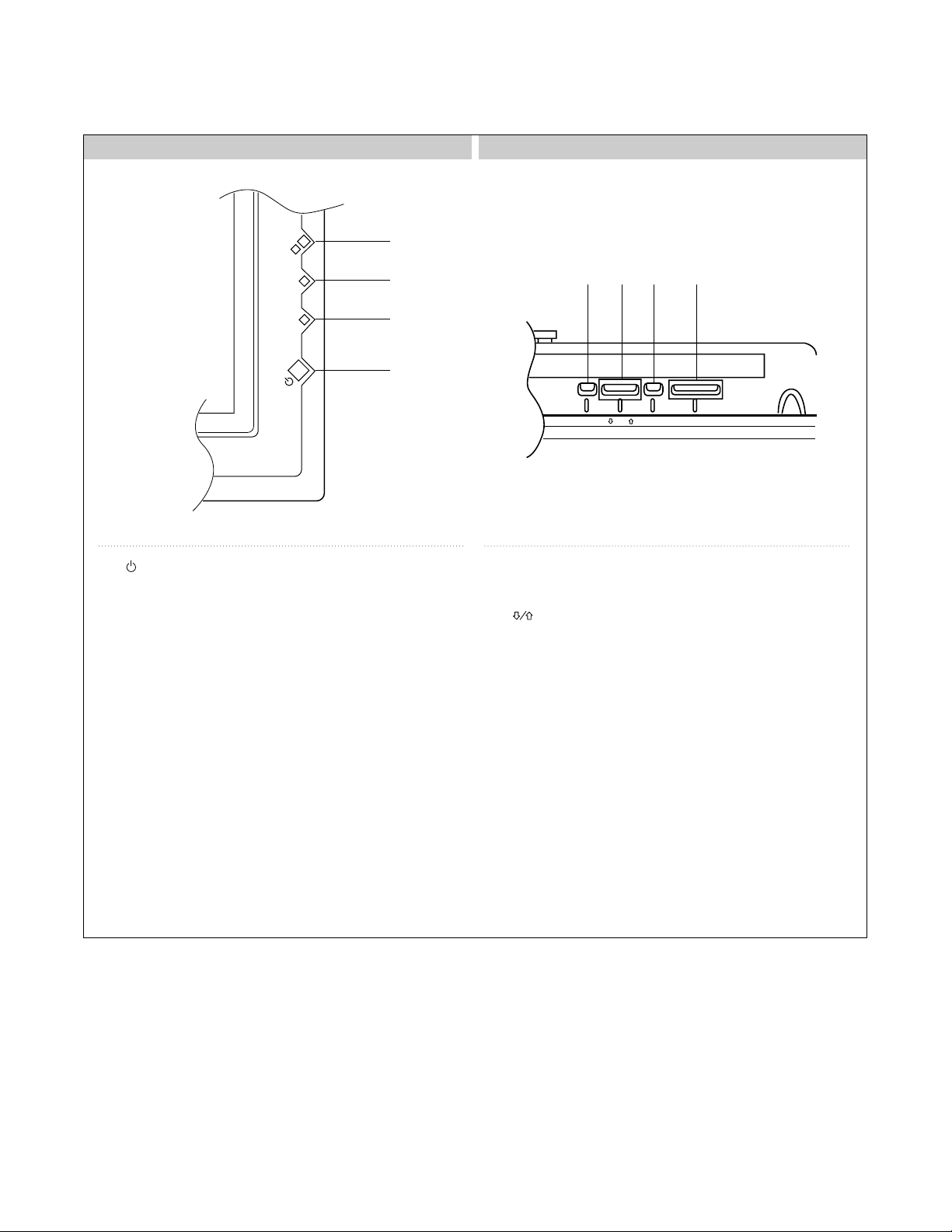
1. (standby)switch
Press to power on the display unit. Press again to
return to the standby mode.
Note
To protect the panel, a certain amount of times is
required to turn unit ON/STANDBY. Wait about
8seconds after one of these operations before
pressing this switch again.
2. STANDBY inducator
Lights up in red in the standby mode.
3. ON inducator
Lights up in green when the diplay unit is powered
on.
4. REMOTE Control detector
Receives the signals from Remote Commander.
- 7 -
Front Control Panel Bottom Control Panel
STANDBY
ON
MENU ENTER
- VOLUME +
1
1
2
3
4
32 4
1. MENU button
Press to show menus. Press again to hide them.
2. buttons
Press to move the cursor(yellow) to an item you
want to select or to adjust a value in a menu.
3. ENTER button
Press to set your choice.
4. VOLUME +/- button
Press to adjust the speaker volume.
- 8 -
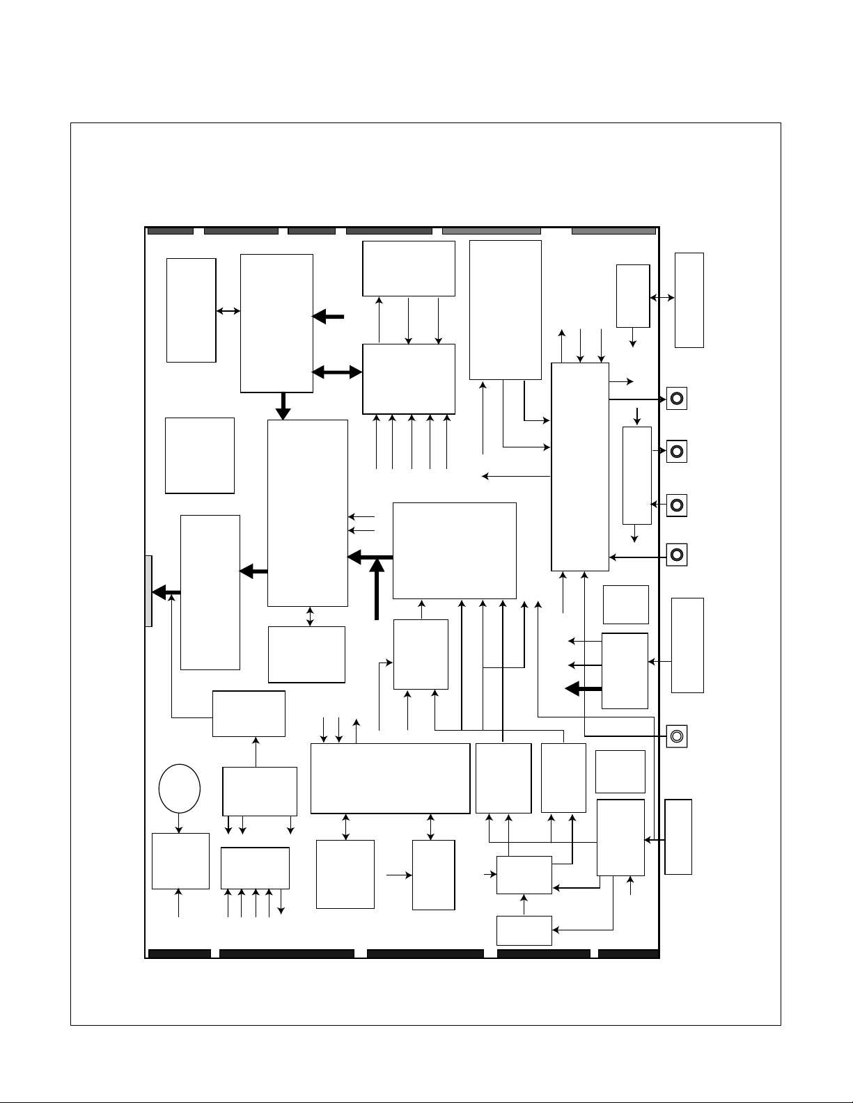
CN19 12Pin
GND
T2
5V
GND
T3
5V
GND
T1
5V
NCNCNC
T-Sense
T-Sense
CPU-IR
Rx/Tx
CN9 7Pin
ACD
RLY
5V-ST
5VD
NC
CN8 12 Pin
5V
5V
5V
GND
GND
GND
GND
GND
9V
9V
12VA
12VA
CN2 10 Pin
PR
GND
Y
GND
PR
GND
HS
VS
GND
DSW
CN6 13P
GND
12V
GND
5VST
GND
GND
RXD
TXD
SDA1
SCL1
26VN
26VN
5Vst
T1
T2
T3
T4
Rea
Timer
(M
Temp.
Sense
(4052)
41T81)
IIC
Bat
OTP
(M27W800)
EEPROM
24C64
DSW
CVM
Sync
(4052)
Sync
Sep
CN22 7 Pin
G-LED2
R-LED2
GND
GND
5VST
STBYIRCN3 4 Pin
KEY1NCGND
3.3VS
CN23 8 Pin9V9V9VNC
GND
GND
GNDNCCN12 Pin
ADOM-OUTR
AUDIO-MUTE
SCL5
SCA5
GND
GND
ADOM-OUTL
GND
12VA
12VA
GND
GND
CN7 15 Pin
GND
GND
SVIDEO-C
GND
GND
GND
SVIDEO-Y
AV1-CVBS
RGB3
Q-SENSE2
Q-SENSE1
GND
AD03-INL
GND
AD03-INR
CN15 4 Pin
26VN
26VN
GND
GND
RGB
Buffer
U-Com
Analog
S/W
Macro.(IIC5)
CXA2171
(BA7657F)
W/TTX
(SDA5550M)
Analog
DDC
(24C21)
TMDS Rx
(Sil161B)
DVI
DDC
(24C21)
A/V Input Select & 6db Amp.
(CXA 2069Q)
Control S In/Out
MAX
232
3D Comb-Filter
(UPD64083)
Video
Decoder
(VPC3230D)
C/C
Z86229
De-Interlace(I/P)
(FLI2310 BC)
Image Processor
ASI 510
(Aurora)
S-Dram
(HY57V643220
CT-6)
S-Dram
(HY57V
643220
CT-6)
ADC9888
(170MHz)
CVM Sync
(4052)
LVDS Tx
(LVDS 83)
Module
Control
12V9V5VST
5V
3.3V
2.5V
1.8V
I/O
Extender
(74LS373)
IIC2
RGB
RGB
H/V
H/V
Sep
SOG
15 Pin D-Sub
DVI D
Remote
5-BNC
Component
48 bit
DST
D-H/V
Sync
Audio 1 In
Audio 3 In
CPU-IR
A/RGB
M/RGB
M/RGB
CVH-Sync
M/H/V
A/H/V
VPC/H/V
CV-Sync
AH/V DH/V
TMDS 48
24 bit
LVDS 31 Pin
To Module
16 bit
8 bit
(Video)
V Out
D/RGB
D/FB
ADC Odd 24 Bit
(Component)
S Video Y
S Video C
M/RGB
CVH-Sync
CVBS-Y
S Video
Y/C
CVBS-C
CVBS Out
CVBS In
Y/C In
Rx/Tx
IR
Audio Pre Out
CVBS Out-In
CVBS Out-In
Audio
In 2
Audio In 3
Audio
Out
Control S
In
Control S
Out
BLOCK DIAGRAM(MAIN)

- 9 -
DESCRIPTION OF BLOCK DIAGRAM
1. Input selection circuit
At BA7657F(IC4) Video signal selects between PC
RGB signal and Component signal.
Then selected output inputs to AD9888(IC12).
2. A/D Converter
This block is composed of AD9888(IC12) and
peripheral devices.
AD9888(IC12) includes A/D converter, Pre-amp, and
PLL.
The basic RGB signal from D-sub RGB and
Component signal Y/Pb/Pr are input to R,G,B pin of
AD9888(IC12).
Input video signal is amplified, Phase locked , A/D
converted to RGB/YUV each 8bits digital signal by
this IC(IC12).
And send the Digital video signal to ASI510(IC14).
IC12 makes clock for ASI510(IC14).
3.TMDS Receiver
This Block is composed of SiI161B (IC17) and
peripheral devices.
This ICs decodes TMDS Input signal from DVI-D Pin
(CN5) and make 48bit digital signal to send Digital
signal to ASI510(IC14).
4. Micom & DDC Controller part
This block is composed of SDA5550M(IC3) and OPT
Memory(IC33),expanded I/O Expender IC(IC2,
IC8,IC36) and EEPROM IC(IC1,IC34,IC49).
SDA5550M controls peripheral devices through IIC
line.
Major functions are
(1) to store user setting value in the IC1.
And (2) to store EDID data in the EEPROM
(IC34,IC49)
5. Video Decoder Circuit
This block is composed of VPC3230D(IC601) and
peripheral devices
SDA5550M(IC3) controls this IC through IIC Line.
This IC analyzes input signal of CVBS, Y/C, Y/Pb/Pr
and output analyzed signal (8bit interlace signal) to
De-interlace block.
Analyzed signal has video control signals like
Contrast, Brightness, Sharpness, Color, tint signals
Including Adaptive Comb Filter.
Input CVBS from 3d Comb filer IC(IC31) is
seperarated to Y and C. And passed by
LPF(L501,L502).
Then inputed to Audio/Video switch(IC41).
6. DTV Circuit
This block is composed of AD9888(IC12) and
peripheral devices
AD9888(IC12) includes A/D converter, Pre-amp, and
PLL.
This circuit is controlled by SDA5550M(IC3) from IIC
Line.
The function is that Component signal(Y/Pb/Pr) from
Component(CN2,CN10) pass by control and output to
ASI510.
7. Audio Decoder Circuit
This block is composed of TPA3002D2(IC10) and
peripheral devices.
SDA5550M(IC3) controls this IC through IIC Line.
This IC analyzes Audio input signal through A/V Jack
and PC1/2 audio, DVD/DTV audio.
8. De-Interlacer
This block is composed of FLI2310(IC10) and
peripheral devices.
SDA5550M(IC3) controls this IC through IIC Line.
And this IC convert 8 Bit Interlace Y/UV signal to Deinterlace signal.
It output converted signal to 16 Bit YUV signal
9. Panel-Link Circuit
LVDS Transmitter THC63LVDM83R(IC44) is the IC
that receives output digital signal of ASI510(IC14) and
output to PDP Module.
The signal format is LVDS.
PDP Module has LVDS receiver that is same output
of ASI510(IC14).
This is the best for reduction EMI problem and the
number of pin connector.
10. 3D Comb filter
In case of NTSC Composite VIDEO signal, Color and
Y are separated by 3D Comb filter IC UPD64083
(IC31). Then inputted to Video decoder IC
VPC3230D(IC601).
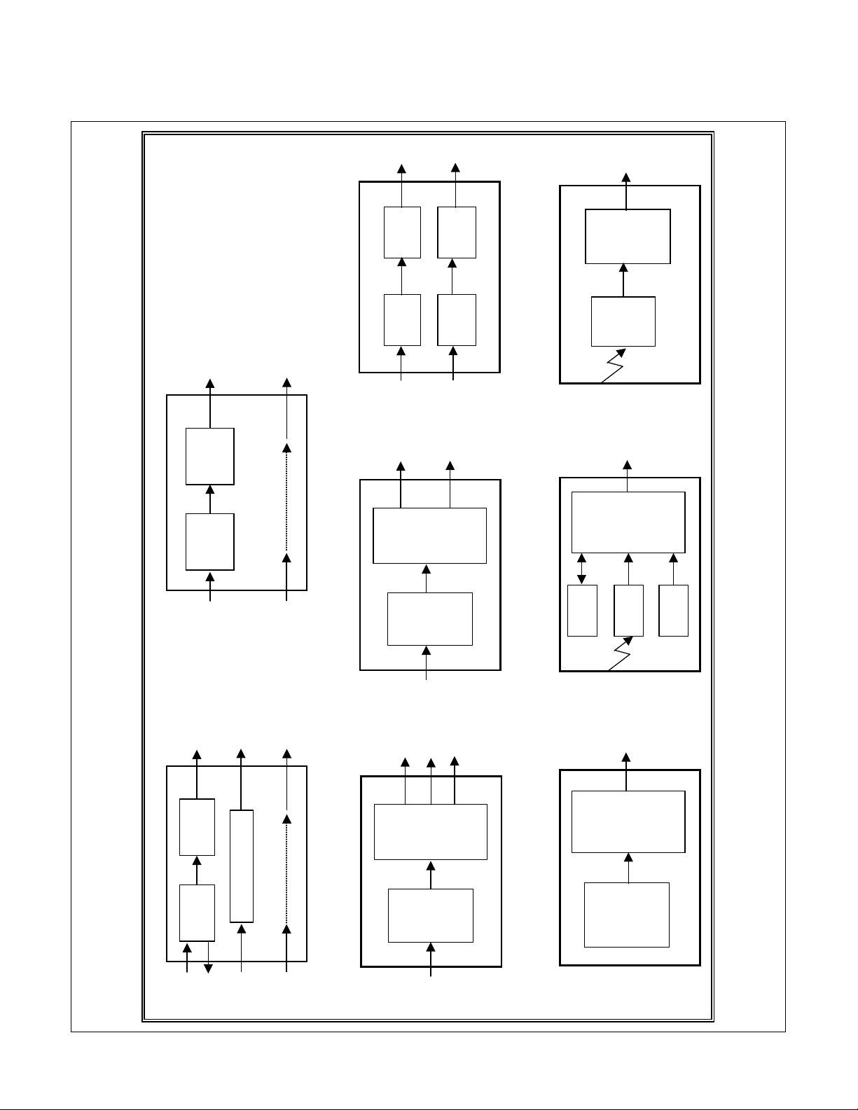
Block Diagram(Others)
- 10 -
Wafer, 44P,
PCN10C
-44S
Wafer, 10P,
13P and 15P
From
Option
Board
#1,#2
To
Main
VS
Board
SUB Board Assy
Tact SW,
Menu/
Down,Up/
Ente r/
Vol Down,Up
Wafer, 4P
To
Main
VS
Board
Key Control Board Assy
Remote Control Board Assy
Wafer, 7P
To
Main
VS
Board
LED,
GN/RD
Infra-R ed
Recei
ver
SW, Power
From
Audio
Amplifier
Board
To
Speak er
R/L
Speaker Jack Board Assy
Audio Amplifier Board Assy
To
Speaker
Jack
Board
Right
Sound Out
Left
Sound Out
Right
Sound Out
Left
Sound Out
Temp
Sensor,
LM350Z
To
Main
VS
Board
Temperature Sensor Board Assy
OP
Amp,
KA358
Composite
(CVBS)
To
Sub
Board
Option #1 Board Assy
Option #2 Board Assy
From
Main
VS
Board
Audio
Process,
TA1343N
Audio
Amplifier,
TPA3002
CVBS
IN
CVBS
Out
Buffer
Y/C
IN
Buffer
Audio
IN
CVBS
Out
Y/C
Out
Audio
Out
Component
To
Sub
Board
Component
IN
Buffer
Audio
IN
Component
Out
Audio
Out
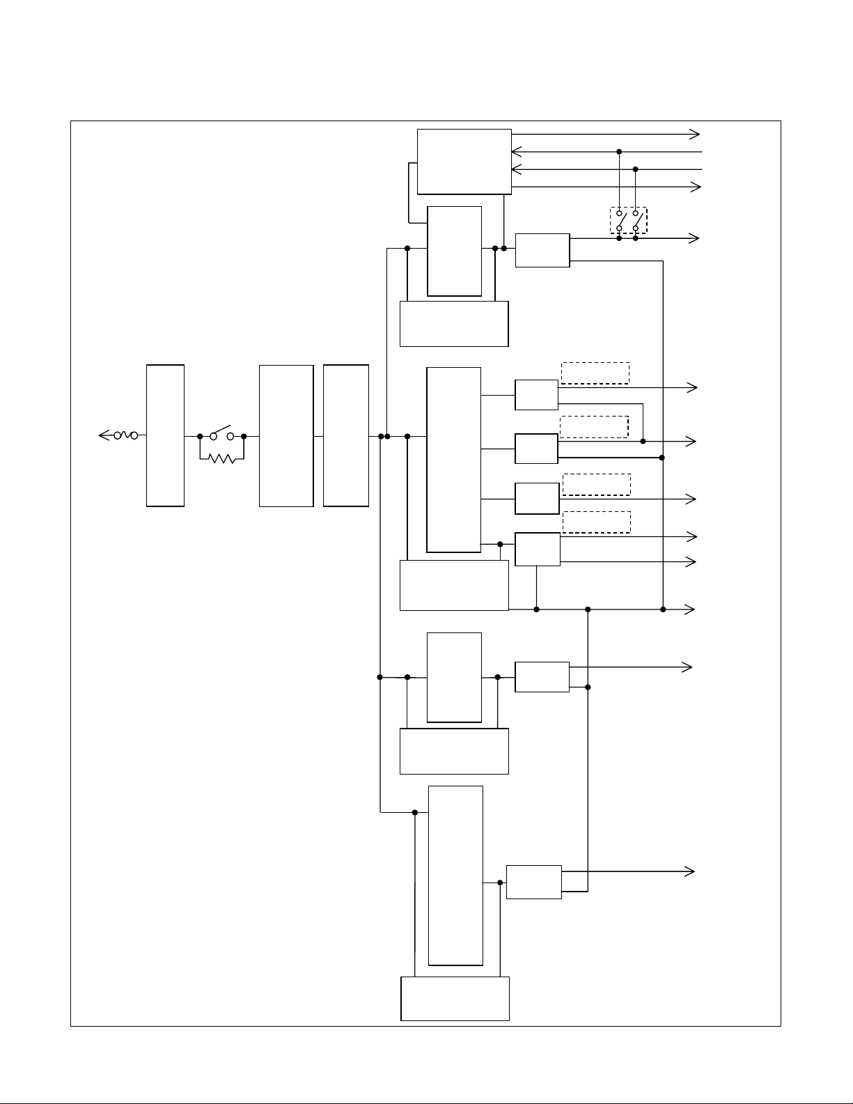
Block Diagram(Power)
- 11 -
AC INPUT
PFC
Rectifer
bridge
connection
Input
Filter
+5V
Flyback conv.
T1
Supervisory
AC-Det
Relay-on
5V-Det
5Vctrl
+5V
9Vsc
Flyback conv.
T2
T3
+60V
T4
+190V
GND
Va
Stand-by 5V
26Vnet
5Vsc
Vs-on
+9V
Vs
RL1
using a CSD
and
Sequence
control
using a CSD
Flyback conv.
using a CSD
Flyback conv.
+14V
+12V
12Vaudio
Voltage Regulator
Voltage Regulator
Voltage Regulator
Voltage Regulator
SW1

- 12 -
ADJUSTMENT
1. Procedures of how to go to service mode.
1) Enter the service mode of this unit by turning on the
power while pressing and holding the "↓" key
simultaneously.
2) Press "MENU" key----MAINTAIN.
3) Press "OK" key to enter the service menu.
4) Select the desired function.
5) Press the "MENU" key to exit OSD.
6) Turn off the power and then turn on it again. The
monitor then enters the normal mode.
To enter the service again, repeat the procedure
described above.
Note
W/B readjustment is required after the panel, board
and microcomputer are replaced. However, be sure to
perform aging for more than 30 minutes for RGB reset
before W/B adjustment.
2. Setup
1) Prepare timing and pattern data for a signal
generator according to the Sony timing specifications.
2)
Connect a monitor video cable to the signal generator.
3) Put Color Analyzer(ex. CA-110) 50cm away from the
monitor, specify it vertically in the center of the
display, and adjust the focus to the optimum level
using an eyepiece.
4) Put the monitor and Color Analyzer(ex. CA-110) in a
light-shielded room.
5) Set up [SERVICE MODE] of the monitor.
3. Operation
Data is manually set to improve the productivity. The
brightness, contrast, and backlight are set to 50, 70
and 100 respectively. After that, the default data of the
color temperature to be adjusted is set.
4. Warm up time
Warm up for 30 minutes before performing any
adjustment.
5. Adjustment for White Balance
a. Display SMPTE at SXGA/60Hz(Input level 0.73V).
b. Set up [SERVICE MODE].
c. Click "INITIAL EEPROM" and again setup Service
Mode.
d. Click "WHITE BALANCE"
6. 11000K color adjustment
a. Select "11000K" in "COLOR TEMP" and enter.
b. Use a 100%(100IRE) Full white video field in
the primary mode.
c. Adjust "RGB GAIN " to secure the color
temperature.
d. Press "MENU" key to exit adjust mode.
7. 9300K color adjustment
a. Select "9300K" in "COLOR TEMP" and enter.
b. Repeat the adjustment procedure as steps b to d at
11000K.
8. 6500K color adjustment
a. Select "6500K" in "COLOR TEMP" and enter.
b. Repeat the adjustment procedure as steps b to d at
11000K.
- 13 -
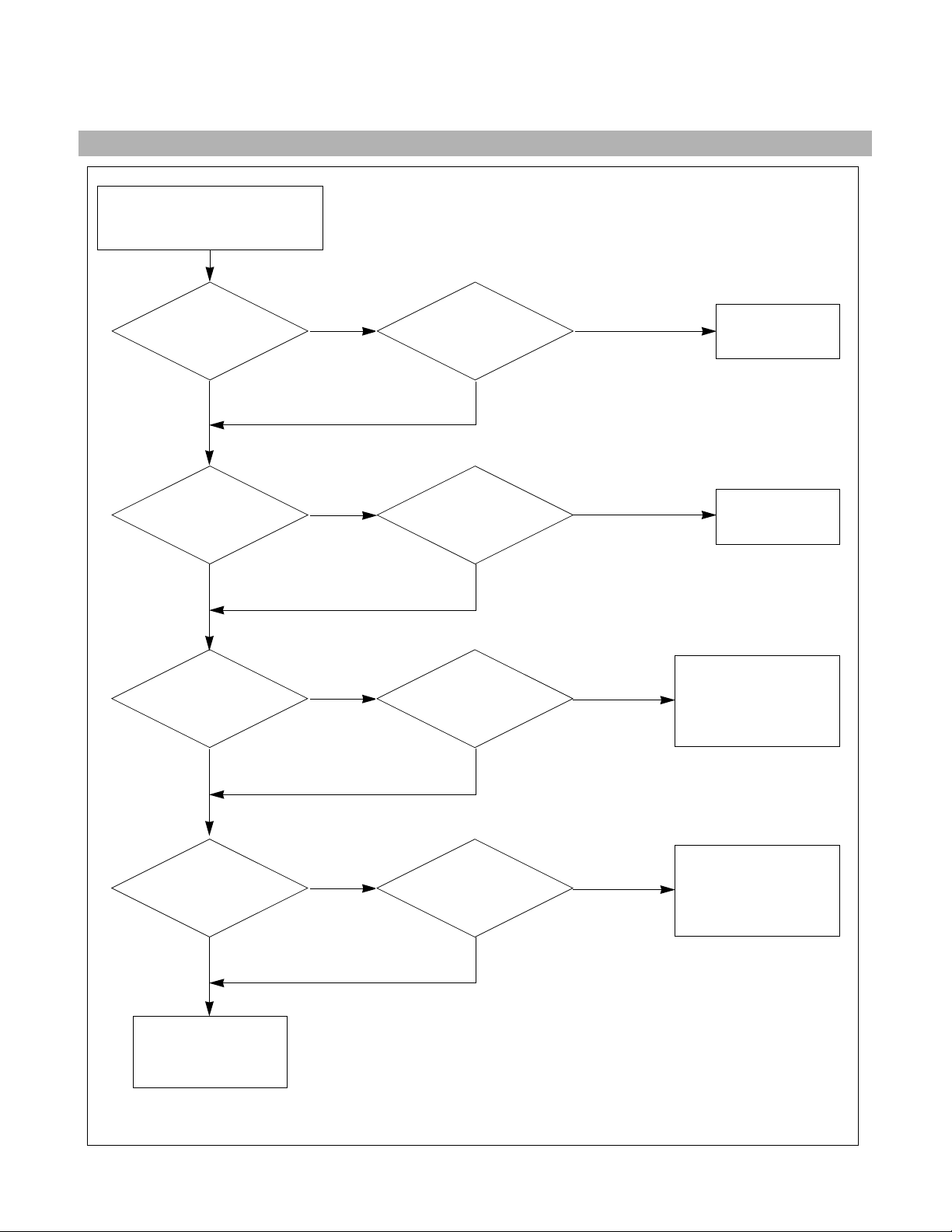
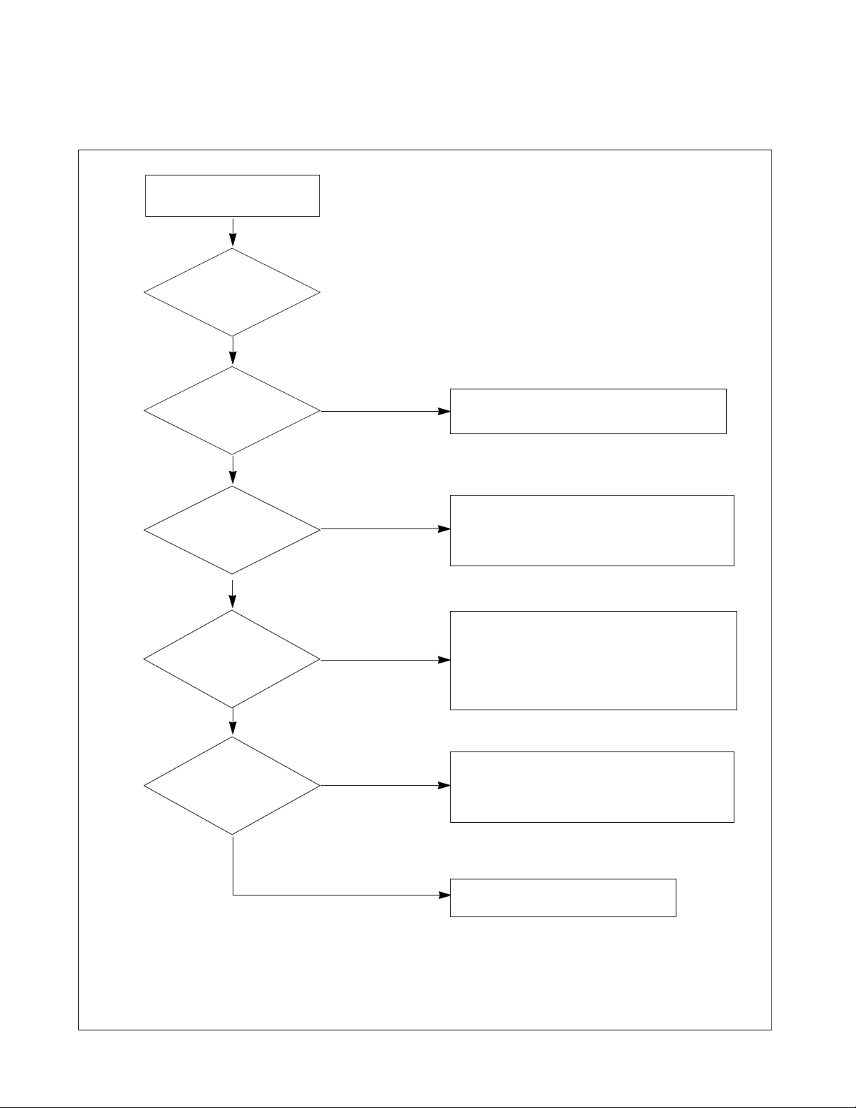
TROUBLESHOOTING GUIDE(MAIN)
1. OUT OF ORDER ON POWER
Check Ctrl signal
CN9 (Pin#2)
‘RLY’
NO POWER
Replace
the Power B’d
Check 5V-ST
CN9(Pin#3)
Check
Connector or
5V-ST Output
On Power B’d
Check
IC8 (Pin #6)
Fail
Fail
Fail
Fail
Check Device
Q35, IC8, IC3
High
Check Ctrl signal
CN9 Pin#1
‘ACD’
Check
IC2 (Pin #3)
Connector or ‘ACD’
Output On Power B’d
Check Device
IC2, IC3
High
Fail
Check Ctrl signal
CN9 (Pin#5)
‘VS07’
Check
IC8 (Pin #9)
Check Device
Q36, IC8, IC3
High
*Check the Power
Cable connection
Pass
Pass
Pass
Pass
Pass
Pass
Pass
Pass
- 14 -
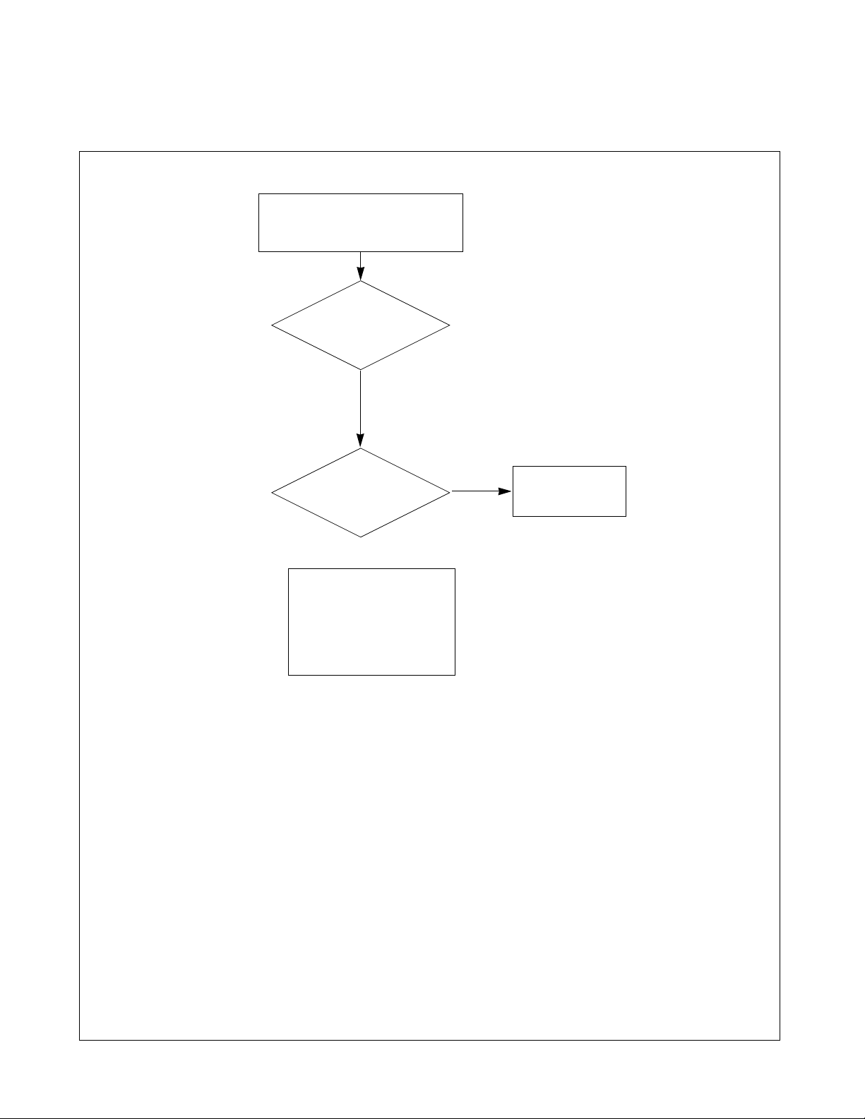
NO RASTER ON DIGITAL
SIGNAL
Rewrite EDID
Data
Repeat
‘A’ Process
Check The
EDID Data
Check IC17(Sil161B)
-H/V Sync
-Output Clock
-Output Data
-Power Down Ctrl Signal
(TMDSRX*-PDN)
Fail
Pass
- 15 -
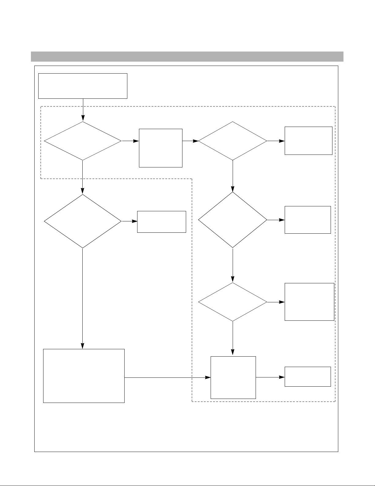
2. NO RASTER STATE
Check
U12(AD9888)
.HSYNC-ADC
.VSYNC-ADC
.DCLK-ADC
.DATA
NO RASTER ON ANALOG
SIGNAL
*Check the Power
: 3.3VDD
*Replace Device
IC21
Check
Power Line
IC21, IC45,
IC20, IC22,
IC23, IC24
Check LED
Status on
Display Head
Check
Ctrl signal IC44
Pin#32
(LVDS83)
Green
3.3V
2.5V
Fail
Replace Device
: IC14, IC15
Replace the
IC14(Scaler)
Find a
Soldering Error
or check the
oscillator(X5)
*Check the D-sub Conn
Connection
- Y/Pb/Pr Jack check
*Check the other Device
- IC26, IC27(SDRAM)
- IC44(LVDS83) Pin#32
Check
Scaler(IC14)
Output
. PCLOCK
. PVSYNC
. PHSYNC
. PVALID
.DATA
Fail
Fail
Pass
*Check Connector
CN501
Check
Control Signal
‘DISPEN’
CN501 Pin #27
Fail
Fail
Fail
Replace Device
.IC21, IC30, IC4
Amber
Pass
Pass
Pass
‘A’ Process
- 16 -
NO RASTER ON Y, Pb, Pr/Y,Cb Cr SIGNAL
Replace Device
Q53, 54, 55, 50, 51, 52
Power S/W off and on
after remove the Input
signal cable
Repeat
‘A’ Process
Input Select
Input 1, Option
Check
Microvision Copy
Protection & Input Select
IC43(CXA2171)
Check
Analog Switch DTV
IC4(BA7657)
Check
IC12(AD9888)
*In/Out H/V Sync
*Output Data
Check
IC10(FLI2310)
*S2310-RESET
*In/Out H/V Sync
*Output Data
Replace Device
Q29, 30, 31,
23, 27, 28
*Check the Power
( 3.3ADCAA, 3.3ADCPA
3.33.3ADCDA)
*Replace Device
IC13
*Check the Power
( 3.3V-DNT, 1.8V-DNT
*Replace Device
IC18, IC11
Fail
Fail
Fail
Fail
Pass
Pass
PassPass
Pass
480P
480i
720P
1080i
Pass
Pass
- 17 -
NO RASTER ON AV SIGNAL
(CVBS, S-VIDEO)
Repeat
‘A’ Process
Check
Input Select for AV
IC41(CXA2069)
Pass
Check
3D Comb Filter
IC31(uPD64083)
Pass
Check
U601(VPC3230D)
*In/Out H/V Sync
*Output Data
*Input Signal
Check
U302(FLI2310)
*VPC-RESET
*In/Out H/V Sync
*Output Data
Pass
Pass
Pass
* Check video signal CN7 Pin#14 AV1-CVBS
* Replace Device
Fail
* Check the power
(3.3VDD-UPD, 2.5VDD-UPD, 2.5VDD-UPD)
* Replace Device
IC40, IC42, Q10, 11,14, 15, 16, 17
Fail
* Check the power
:1.8V-DNT, 3.3V-DNT
* Replace Device
IC18, IC11
Check the Input jack and cable
Fail
* Check the power
(5V-VPC, 3.3V-VPC)
* Replace Device
IC25, IC28, Q4,6,22,12,18, 5,8,7,21,34,
39,20,37,40,21,38, 41, 42, 45, 48, 43, 46, 49,
57, 44, 47, 56
Fail
- 18 -
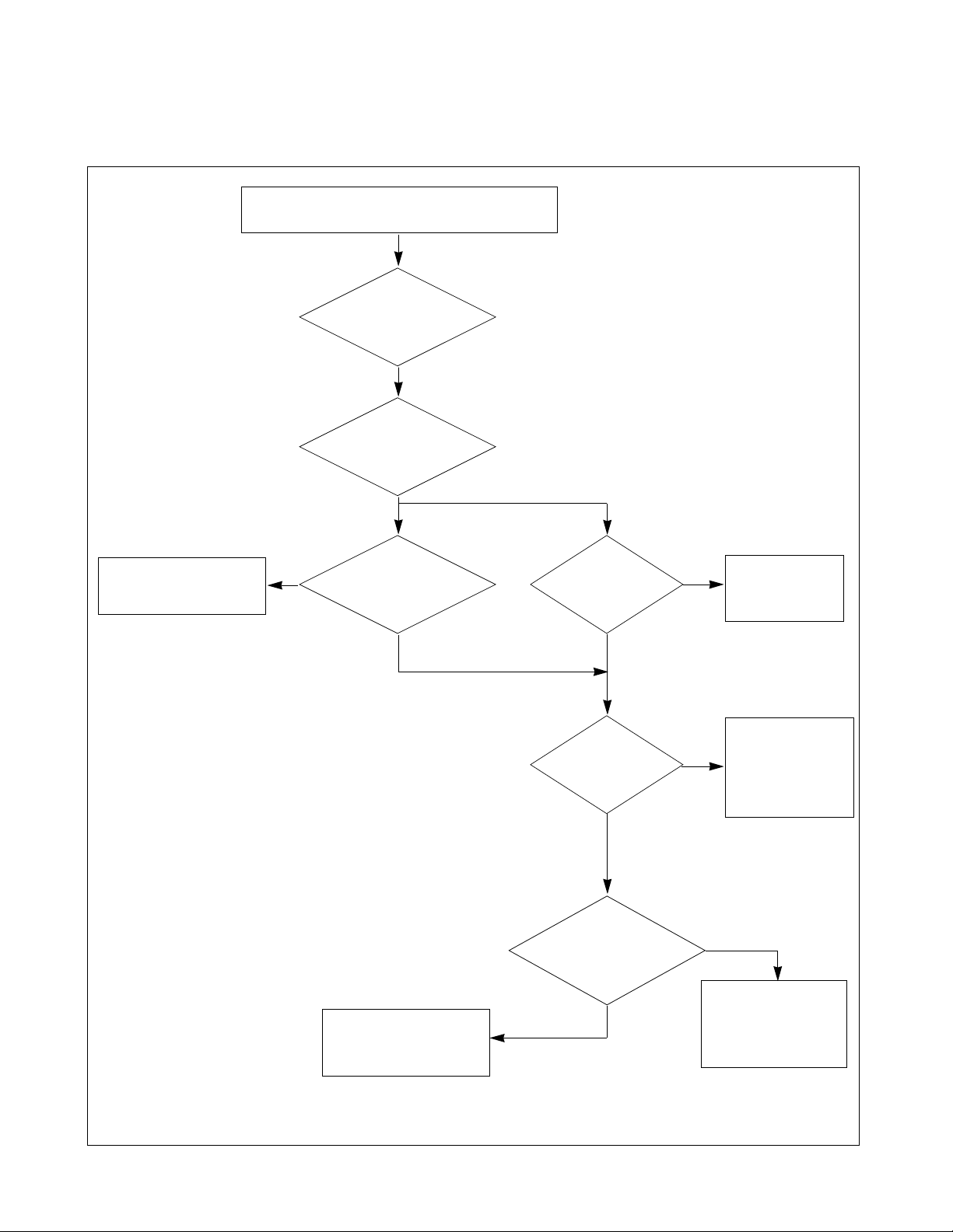
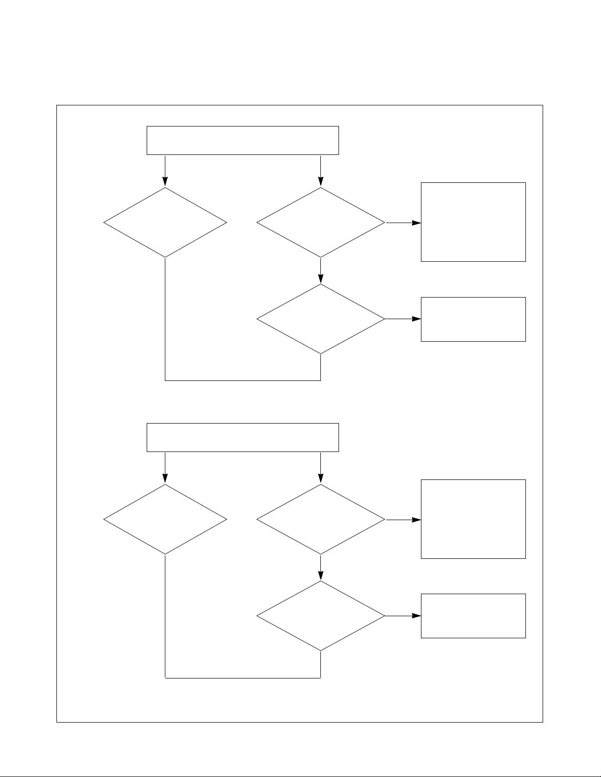
A Process
Check
CN207(44Pin Wafer)
B12,B13,B14,B15,B16
Check
CN2
R/G/B/H/V
VS-Board
Input
Option #2
Input
* Check
CN201, CN202, CN203
CN204,CN205 Input
* Check
5VST, 12V
No Raster On analog Signal
Fail
* Check CN2
10Pin Signal connector
Fail
Yes
A Process
Check
CN207(44Pin Wafer)
B12,B13,B14
Check
CN2
Pb/Y/Pr
VS-Board
Input
Option #2
Input
* Check
CN201, CN202, CN203
* Check
5VST, 12V
No Raster On Y, Pb, Pr/Y, Cb, Cr
Fail
* Check CN2
10Pin Signal connector
Fail
Yes
 Loading...