

Page 1

MODEL: NCS710BRSERVICE MANUAL
Internal Use Only
Website http://biz.lgservice.com
CAR CD/MP3/WMA
RECEIVER
SERVICE MANUAL
MODEL: NCS710BR
P/NO : AFN75512859 SEPTEMBER, 2011
CAUTION
BEFORE SERVICING THE UNIT, READ THE “SAFETY PRECAUTIONS”
IN THIS MANUAL.
Page 2

CONTENTS
SECTION 1 SUMMARY
SERVICING PRECAUTIONS .............................................................................................................................1-2
ESD PRECAUTIONS ..........................................................................................................................................1-3
SPECIFICATIONS ..............................................................................................................................................1-4
LOCATION OF USERS CONTROLS ................................................................................................................. 1-5
HOW TO SETTING THE OPTION CODE ..........................................................................................................1-6
FIRMWARE UPGRADE METHOD ..................................................................................................................... 1-7
HOW TO CONNECT AUDIO SET TO POWER SUPPLY .................................................................................. 1-8
SECTION 2 ELECTRICAL
ELECTRICAL TROUBLESHOOTING GUIDE ....................................................................................................2-1
1. SYSTEM CONTROL ERROR CORRECTION FLOW CHART .................................................................2-1
2. SOUND ERROR CORRECTION FLOW CHART ......................................................................................2-4
3. DISPLAY ERROR CORRECTION FLOW CHART ....................................................................................2-7
4. TUNER ERROR CORRECTION FLOW CHART .....................................................................................2-10
5. CDP ERROR CORRECTION FLOW CHART .........................................................................................2-11
6. USB ERROR CORRECTION FLOW CHART ..........................................................................................2-14
7. BLUETOOTH ERROR CORRECTION FLOW CHART ...........................................................................2-16
8. AUX ERROR CORRECTION FLOW CHART ..........................................................................................2-17
WAVEFORMS ...................................................................................................................................................2-18
CIRCUIT VOLTAGE CHART ............................................................................................................................ 2-20
INTERNAL BLOCK DIAGRAM OF ICS ........................................................................................................... 2-21
1. IC601 (BD3702FV) ...................................................................................................................................2-21
2. IC801 (LV5693P) .....................................................................................................................................2-22
3. IC804 (TB2946HQ) ..................................................................................................................................2-24
WIRING DIAGRAM ...........................................................................................................................................2-25
BLOCK DIAGRAMS .........................................................................................................................................2-27
CIRCUIT DIAGRAMS .......................................................................................................................................2-31
1. MAIN CIRCUIT DIAGRAM .......................................................................................................................2-31
2. DSP_1 CIRCUIT DIAGRAM ....................................................................................................................2-33
3. DSP_2 CIRCUIT DIAGRAM ....................................................................................................................2-35
4. FRONT CIRCUIT DIAGRAM ...................................................................................................................2-37
5. CD CIRCUIT DIAGRAM ...........................................................................................................................2-39
PRINTED CIRCUIT BOARD DIAGRAMS ........................................................................................................2-41
1. MAIN P.C.BOARD ...................................................................................................................................2-41
2. FRONT P.C.BOARD ................................................................................................................................2-43
3. CD P.C.BOARD .......................................................................................................................................2-44
SECTION 3 EXPLODED VIEWS
1. CABINET AND MAIN FRAME SECTION .................................................................................................. 3-1
2. MECHANISM(PICK-UP) SECTION ...........................................................................................................3-3
SECTION 4 REPLACEMENT PARTS LIST
1-1
Page 3

SECTION 1 SUMMARY
SERVICING PRECAUTIONS
1. Always disconnect the power source before:
1) Removing or reinstalling any component, circuit board, module or any other instrument assembly.
2) Disconnecting or reconnecting any instrument electrical plug or other electrical connection.
3) Connecting a test substitute in parallel with an electrolytic capacitor in the instrument.
CAUTION: A wrong part substitution or incorrect polarity installation of electrolytic capacitors may result in an
explosion hazard.
2. Do not defeat any plug/socket B+ voltage interlocks with which instruments covered by this service
manual might be equipped.
3. Do not apply power to this instrument and or any of its electrical assemblies unless all solid-state device heat sinks are correctly installed.
4. Always connect a test instrument’s ground lead to the instrument chassis ground before connecting
the test instrument positive lead. Always remove the test instrument ground lead last.
1) The service precautions are indicated or printed on the cabinet, chassis or components. When servicing,
follow the printed or indicated service precautions and service materials.
2) The Components used in the unit have a specifi ed confl ammability and dielectric strength. When replacing
any components, use components which have the same ratings. Components marked in the circuit diagram
are important for safety or for the characteristics of the unit. Always replace with the exact components.
3) An insulation tube or tape is sometimes used and some components are raised above the printed writing
board for safety. The internal wiring is sometimes clamped to prevent contact with heating components.
Install them as they were.
4) After servicing always check that the removed screws, components and wiring have been installed correctly
and that the portion around the service part has not been damaged. Further check the insulation between
the blades of attachment plug and accessible conductive parts.
1-2
Page 4
ESD PRECAUTIONS
Electrostatically Sensitive Devices (ESD)
Some semiconductor (solid state) devices can be damaged easily by static electricity. Such components commonly are called electrostatically sensitive devices (ESD). Examples of typical ESD devices are integrated circuits
and some fi eld-effect transistors and semiconductor chip components. The following techniques should be used
to help reduce the incidence of component damage caused by static electricity.
1. Immediately before handling any semiconductor component or semiconductor-equipped assembly, drain off
any electrostatic charge on your body by touching a know earth ground. Alternatively, obtain and wear a commercially available discharging wrist strap device, which should be removed for potential shock reasons prior
to applying power to the unit under test.
2. After removing an electrical assembly equipped with ESD devices, place the assembly on a conductive surface
such as aluminum foil, to prevent electrostatic charge buildup or exposure of the assembly.
3. Use only a grounded-tip soldering iron to solder or unsolder ESD devices.
4. Use only an anti-static solder removal device. Some solder removal devices not classifi ed as “anti-static” can
generate electrical charges suffi cient to damage ESD devices.
5. Do not use freon-propelled chemicals These can generate electrical charges suffi cient to damage ESD de-
vices.
6. Do not remove a replacement ESD device from its protective package until immediately before you are ready to
install it. (Most replacement ESD devices are packaged with leads electrically shorted together by conductive
foam, aluminum foil or comparable conductive materials).
7. Immediately before removing the protective material from the leads of a replacement ESD device, touch the
protective material to the chassis or circuit assembly into which the device will by installed.
CAUTION : BE SURE NO POWER IS APPLIED TO THE CHASSIS OR CIRCUIT, AND OBSERVE ALL
OTHER SAFETY PRECAUTIONS.
8. Minimize bodily motions when handing unpackaged replacement ESD devices. (Otherwise harmless motion
such as the brushing together of your clothes fabric or the lifting of your foot from a carpeted fl oor can generate
static electricity suffi cient to damage an ESD device).
CAUTION. GRAPHIC SYMBOLS
THE LIGHTNING FLASH WITH ARROWHEAD SYMBOL. WITHIN AN EQUILATERAL TRIANGLE,
IS INTENDED TO ALERT THE SERVICE PERSONNEL TO THE PRESENCE OF UNINSULATED
“DANGEROUS VOLTAGE” THAT MAY BE OF SUFFICIENT MAGNITUDE TO CONSTITUTE A
RISK OF ELECTRIC SHOCK.
THE EXCLAMATION POINT WITHIN AN EQUILATERAL TRIANGLE IS INTENED TO ALERT
THE SERVICE PERSONNEL TO THE PRESENCE OF IMPORTANT SAFETY INFORMATION IN
SERVICE LITERATURE.
1-3
Page 5

SPECIFICATIONS
• General
Output Power 53 W x 4 CH (Max.)
Power Source DC 12 V
Speaker impedance 4 Ω
Ground System Negative
Dimensions (W x H x D) (178 x 50 x 169) mm (without Control Panel)
Net Weight 1.37 kg
• TUNER
FM Tuning Range 87.5 MHz to 108.0 MHz
S / N Ratio 55 dB
Distortion 0.7 %
Usable Sensitivity 12 dBμV
AM (MW) Tuning Range (520 to 1720) kHz or (522 to 1620) kHz
S / N Ratio 50 dB
Distortion 1.0 %
Usable Sensitivity 28 dBμV
• CD
Frequency Response 20 Hz to 20 kHz
S / N Ratio 80 dB
Distortion 0.12 %
Channel Separation (1 kHz) 55 dB
• AUX
Frequency Response 20 Hz to 20 kHz
S / N Ratio 80 dB
Distortion 0.1 %
Channel Separation (1 kHz) 45 dB
Max Input Level (1 kHz) 1.1 V
• USB
Version USB 1.1 or USB 2.0 Full Speed
Bus Power Supply (USB) DC 5 V 1 A
• SD
Distortion 0.1 %
• Line OUT
Frequency Response 20 Hz to 20 kHz
Output Voltage 2 V (Max.)
• Subwoofer
Frequency Response 20 Hz to 120 Hz
Output Voltage 2 V (Max.)
Design and specifi cations are subject to change without notice.
1-4
Page 6
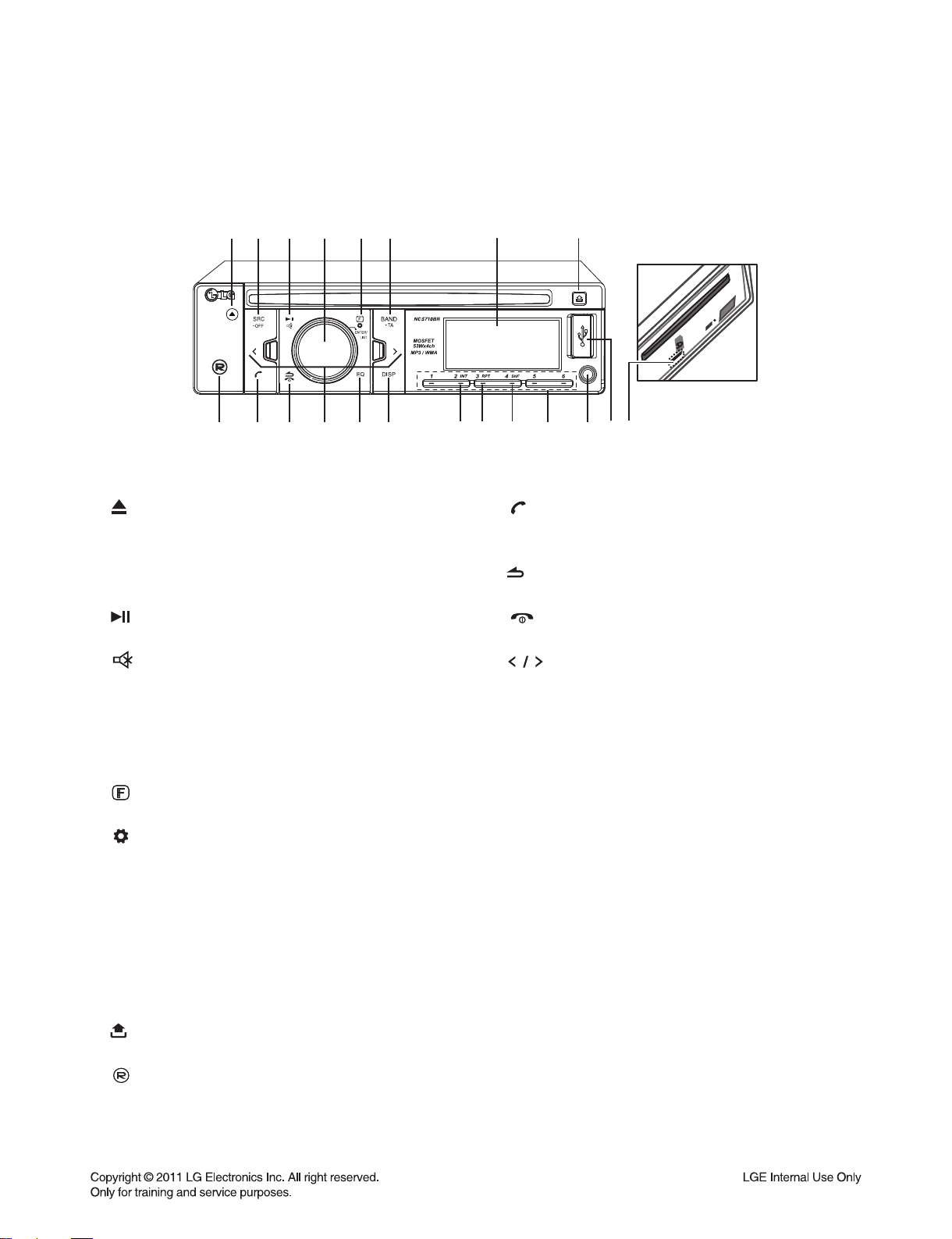
FRONT PANEL
A
I
LOCATION OF USERS CONTROLS
BC D EF G
[Front unit detached panel]
JK L MN OPQHRSTU
A
Ejects a disc.
B SRC/ • OFF
- When pressed, selects function sources.
- When pressed and held, powers unit on or off.
C
Plays and pauses playback.
Temporarily stops the sound.
D Volume knob
- Adjusts volume level.
- Confi rms the settings.
- Checks tracks, files or preset stations.
E
In each mode, sets playback items.
Activates setting menu.
F BAND
- Selects a band in Tuner mode.
- Moves to a next USB drive.
• TA
- Searches stations that have TA / TP
information, when it is pressed and held.
G Display window
H
Opens the front panel.
I
Recording to USB / SD card.
J
- Activates BT function.
- Answers a call.
K
Returns to the previous step.
Ends a call.
L
Skip/ Search/ Seek/ Tune
M EQ
Improves sound quality.
- When pressed, selects the EQ function.
N DISP
- Press it, you can check the clock time.
- Press and hold it, you can turn on/off the
display window and the light of LED buttons.
O INT
Intro scan.
P RPT
Repeats playback.
Q SHF
Shuffl es playback.
R Numeric buttons (1 to 6)
Selects a numbered preset station in TUNER.
S AUX
If connected to other portable player, you can
enjoy music from it on the unit.
T USB port
U SD card slot
1-5
Page 7
HOW TO SETTING THE OPTION CODE
1. Option Table
Option Codes for Car CD products of 2011 will be defi ned as below
* OPTION TABLE
INDEX AREA RDS OPTION CODE SUFFIX
1 EU SUPPORT 111
2 EU SUPPORT 112 ERUSLL*
3 EU PS_RT_ONLY 121
4 S.America PS_RT_ONLY 221
EDEULL*
EDZALL*
EESPLL*
EHUNLL*
EMARLL*
ESWELL*
ETUREL*
EZAFLL*
EINDLL*
EIRNJL*
EISRRL*
ENGALL*
ESAUBL*
YEGYIL*
ECHLLL*
ECOLLL*
EPANLL*
PBRALL*
YMEXCL*
The option code is comprised of 3 digits and each digit has a range 1~6.
In the 2011, Car CD Product has totally four option codes from entire suffi xes.
2. Operation
1. Entering Option Setting Function
1) Power off on the radio source.
2) Push and hold the SRC(PWR) Key for 5 seconds, then It goes to the version display mode.
3) Push BAND Key until the LCD displays “OPTION(OPTN) XYZ”.
(The XYZ means the Option Code)
2. How to change the option code
1) The Input mode can be set by press the volume knob, the fi rst digit will be blinking until the
new code is set.
2) The number what you want to input could be selected by spinning the volume knob clockwise or
counterclockwise.
And then, if you push the volume knob, the selected number will be changed and the focus is moving
to the next.
You can also input the new option code of 1~6 by using preset keys if they are on the front panel.
3) If the new option code is acceptable, “SUCCESS XYZ” will be displayed on the LCD, and then it’ll reset
soon automatically.
4) If the new option code is not acceptable, “CODE ERR” will be displayed on the LCD.
To retry to change the option code, push the volume knob again.
1-6
Page 8

FIRMWARE UPGRADE METHOD
[ MAIN AND CD/USB FIRMWARE UPGRADE ]
1. Confi rmation of version information
• Change the Source of audio set to tuner. (Default: tuner)
• Turn power off using power key.
• Press power key for 5 s. (After power on, continue pressing)
• After 5 s, beep sound rings two times.
Then version information would show up at display.
• In order to check version of MAIN and CD/USB system, Press band key.
2. Upgrade Program reading
• Insert update CD or USB in ACC on state and then is displayed in order.
CD : [Reading → File Check → Download?], USB : [USB Check → Download?]
3. Upgrade start
• In order to start upgrade, Press preset 1 Key until “CHECK CD” Display on the LCD.
4. Upgrade progress display
• Upgrade is in progress now.
[ CHECK CD → ERASE → WRITE → I-VRF → D-VRF ]
5. Upgrade Completion
• When Upgrade fi nished, the display shows up “DOWN OK”. After a while, the audio set is
reset automatically.
• Caution!
If power is off on the way of upgrading fi rmware, the set can’t be recovered.
Therefore pay lots of attention for power not to be off.
1-7
Page 9
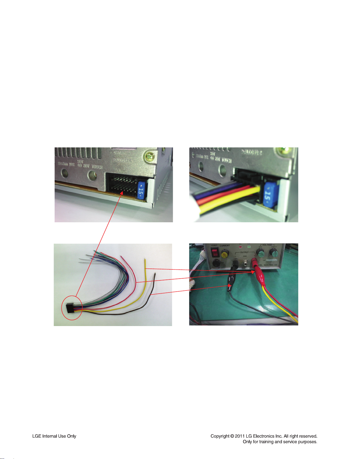
HOW TO CONNECT AUDIO SET TO POWER SUPPLY
• It is suffi cient only to supply power for upgrade.
• Shown from the right fi gure, connect yellow line (Battery) and red line (Ignition) to plus and minus terminal
respectively.
• Jack is connected to the audio set via its shapes matched each other.
• We need power supply for operation of audio set (Voltage : 12~15 V Current : Over 2 A)
Before connection between set and power supply, adjust voltage level to 15 V typically (It is okay up to 12 V.)
Power Supply has a variety of shapes and capacity of voltage and current.
At fi rst check these things.
1-8
Page 10
SECTION 2 ELECTRICAL
ELECTRICAL TROUBLESHOOTING GUIDE
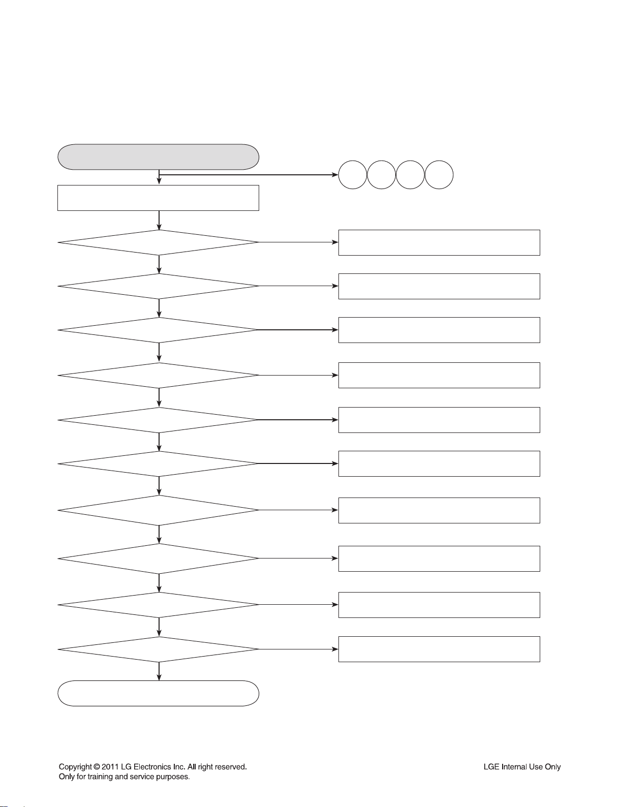
1. SYSTEM CONTROL ERROR CORRECTION FLOW CHART
Something wrong with the System control?
1A 1B 1C 1D
No power?
YES
Checked the Fuse?
YES
Checked the Back up
VDD and GND?
YES
Checked the Regulator
Back up VDD?
YES
NO
NO
NO
F301 Inside of JK801
JK801(1, 2, 3)
IC801(15, 14)
Checked the Main Micom
B+ Detect?
YES
Checked the Main
Micom VDD?
YES
Checked the Main
Micom GND?
YES
Checked the Main
Micom reset?
YES
Checked the Main
Micom X-tal?
YES
Checked the ACC in?
YES
Checked the Front
Panel Key input?
YES
NO
IC401(56)
NO
IC401(30, 47, 50, 99, 100)
NO
IC401(20, 51, 97, 98)
NO
IC401(90), IC402
NO
X401, X402
NO
Q802, R459, IC401(4)
NO
IC401(53, 54), CN402(7, 8)
OK
2-1
Page 11
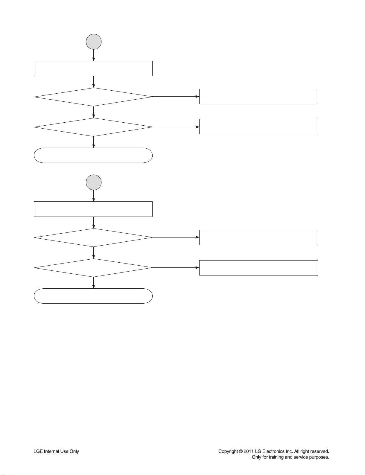
1A
Not available to Volume control?
YES
Checked the
Encoder volume?
YES
Checked the
Volume IC control?
YES
OK
1B
Not available to Key control?
YES
Checked the
Tact switch?
YES
Checked the
Key line?
NO
EV901, IC401(82, 83), CN402(14, 15)
NO
IC401(28, 29), IC601(25, 26)
NO
SW901~SW918
NO
IC401(53, 54), CN402(7, 8)
OK
YES
2-2
Page 12

1C
Not available to Telephone Mute?
YES
Checked the
Tel Mute input?
YES
Checked the
Mute control?
YES
OK
1D
Not available to ANT(Motor Type) control?
YES
Checked the
ANT control?
NO
D811, Q805, Q806, IC401(11)
NO
IC401(21, 27), IC804(22)
NO
D808, IC801(6, 11), IC401(23)
OK
YES
2-3
Page 13
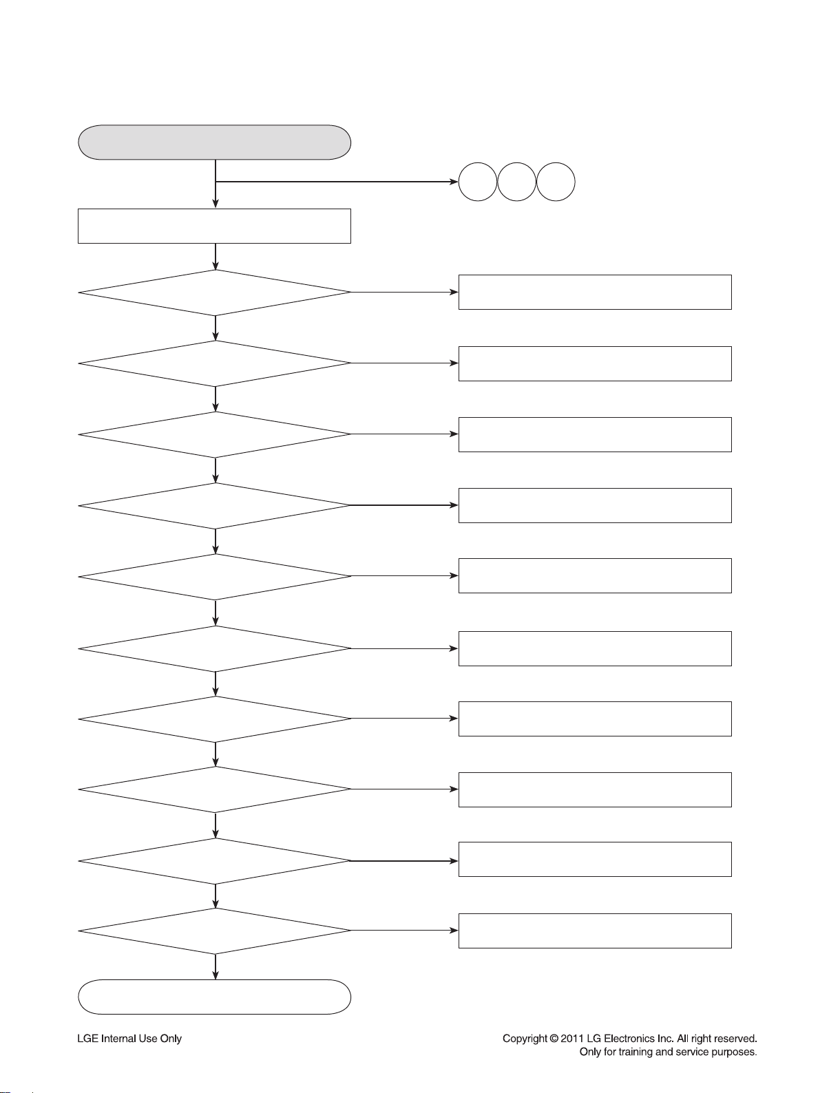
2. SOUND ERROR CORRECTION FLOW CHART
Something wrong with the Sound?
2A 2B 2C
No sounds of All Functions?
YES
Checked the
E-VR VDD?
YES
Checked the
E-VR GND?
YES
Checked the
E-VR control?
YES
Checked the E-VR
Mute control?
YES
Checked the E-VR
Signal in/out?
YES
Checked the
Power IC VDD?
YES
NO
NO
NO
NO
NO
NO
IC601(24)
IC601(27)
IC601(25, 26), IC401(28, 29)
IC601(15), IC401(27)
IC601(1, 2, 3, 4, 5, 6, 7, 9,
18, 19, 20, 21, 22, 23)
IC804(6, 20)
Checked the
Power IC GND?
YES
Checked the
Power IC control?
YES
Checked the Power
IC Signal in/out?
YES
Checked the
Main connector?
YES
OK
NO
NO
NO
NO
IC804(1, 2, 8, 13, 18, 24)
IC804(4, 22), IC401(18, 21)
IC804(3, 5, 7, 9, 11, 12, 14,
15, 17, 19, 21, 23)
JK801(11, 12, 13, 14, 15, 16, 17, 18)
2-4
Page 14
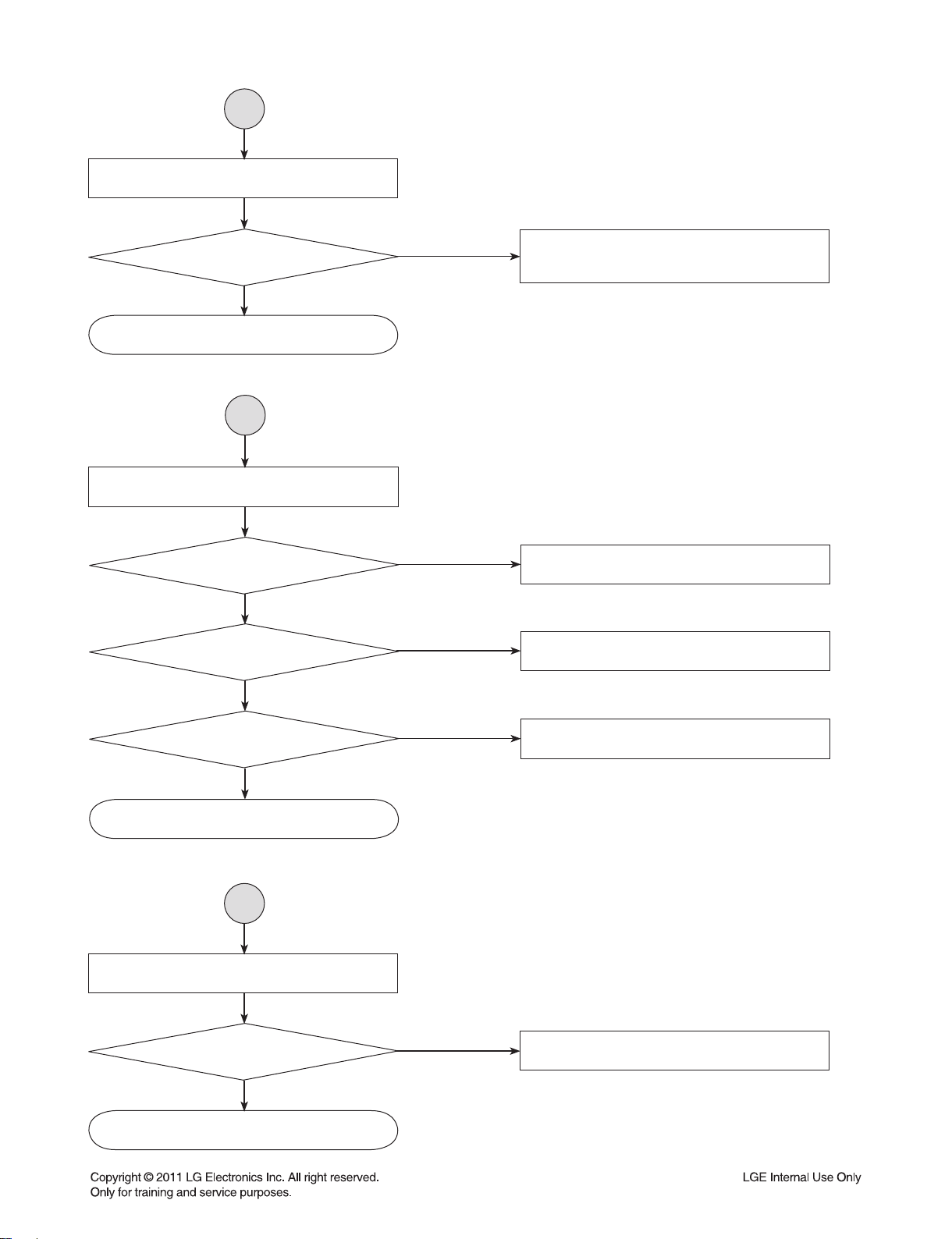
2A
Hearing the Pop Noise?
YES
Checked the
Mute contorl?
YES
OK
2B
No Sound External AMP?
YES
Checked the
Line Out signal?
YES
Checked the Line Out
AMP Mute control?
YES
NO
NO
NO
IC401(21, 25, 27), IC601(15), IC804(22),
Q601, Q602, Q603, Q604, Q607
IC601(18, 19, 20, 21, 22, 23)
Q601, Q602, Q603, Q604, Q607
Checked the Line Out
AMP signal in/out?
YES
OK
2C
No output Beep sound?
YES
Checked the
Beep control?
YES
OK
NO
JK601
NO
IC401(80), IC601(14)
2-5
Page 15

■ CAUTION - Tip for repair
Before exchange power amp IC(TB2946) for no audio problem, you have to check
below list.
1. Check VCC (pin 20, 6) & GND
2. Check input pin 11, 12, 14, 15
3. Check Standby, pin 4
: Follow the below list.
4. Check Mute function, pin 22
: Follow the below list.
Stand-by Power Sound Voltage
ON OFF OFF 0 to 1.5
OFF ON ON 3.5 to 6 V
5. Check Ripple pin 10.
: Normally it is high (about 10 V)
Mute Sound Voltage
ON OFF 0 to 1.5
OFF ON 3.5 to 6 V
6. Re-soldering all the pin of IC.
: Prevent crack of solder line.
* Keep changed IC, We request that you send it to HQ.
C1
C1
C6
C1
C1
PRE-GND
1 20 6
TAB V
CC1VCC2
OUT1
()
+
IN1
11
IN2
12
AC-GND
16
IN3
15
IN4
14
13
STBYRIP
10 25 22
2
C
4
OFF-SET
DET
PW-GND1
OUT1 ( )
OUT2 ( )
PW-GND2
OUT2 ( )
OUT3 ( )
PW-GND3
OUT3 ( )
OUT4 ( )
PW-GND4
OUT4 ( )
MUTE
4
C
9
8
7
+
5
2
3
+
17
18
-
19
+
21
24
-
23
R
1
Picture 1) Power IC desc.
5
C
3
C
R
L
R
L
R
L
R
L
5 V
PLAY
MUTE
: PRE-GND
: PW-GND
2-6
Page 16

3. DISPLAY ERROR CORRECTION FLOW CHART
Something wrong with the Display?
3A 3B
No Display or Some Display is broken?
YES
Checked the LCD
Driver VDD?
YES
Checked the LCD
Driver GND?
YES
Checked the LCD
Driver reset?
YES
Checked the LCD
Driver OSC?
YES
Checked the LCD
Driver data interface?
YES
OK
NO
NO
NO
NO
NO
LCD1(7)
LCD1(10)
LCD1(5), IC401(74)
LCD1(6)
IC401(74, 75, 84, 86), CN402(9, 10, 16, 18),
LCD1(2, 3, 4, 5)
2-7
Page 17

3A
Not available to illumination with button?
YES
Checked the Dimmer
control input?
YES
Checked the
Red LED VDD?
YES
Checked the
Red LED?
YES
OK
YES
Checked the
Blue(Green) LED VDD?
NO
JK801(5), IC801(6)
NO
IC801(1), Q807, IC401(13)
NO
LD921~LD942
NO
IC801(1), Q804, IC401(14)
YES
Checked the
Blue(Green) LED?
YES
OK
NO
LD951~LD972
2-8
Page 18

3B
Not available to LCD Lighting control?
YES
Checked the Dimmer
control input?
YES
Checked the
White LED VDD?
YES
Checked the
White LED?
YES
OK
NO
JK801(5), IC801(6)
NO
IC801(1), Q808, IC401(12)
NO
LD991~LD994
2-9
Page 19

4. TUNER ERROR CORRECTION FLOW CHART
Something wrong with the Tuner system?
Not available to Tuner?
YES
Checked the
Tuner VDD?
YES
Checked the Tuner
VDD control?
YES
Checked the
Tuner GND?
YES
Checked the E-VR
Mute control?
YES
Checked the
I2C data?
YES
Checked the
Audio signal?
NO
IC101(6, 22)
NO
IC801(4, 5), IC401(24), D817
NO
IC101(5, 10, 17, 23)
NO
IC601(15), IC401(27)
NO
IC101(18, 19), IC401(1, 2)
NO
IC101(8, 9)
OK
YES
2-10
Page 20

5. CDP ERROR CORRECTION FLOW CHART
Something wrong with the CD Player?
5A 5B 5C
No Loading?
YES
Checked the CD VDD?
YES
Checked the CD
DSP GND?
YES
Checked the Motor
DRV VDD?
YES
Checked the CD
DSP reset?
YES
Checked the CD
DSP X-tal?
YES
Checked the Disc in
load switch?
NO
NO
NO
NO
NO
NO
Fig 1, 2
IC801(3, 7)
IC302(19, 65, 66, 71, 126, 140, 154, 157)
IC502(7, 8, 20)
IC302(130)
X301(27 MHz)
CN501(2)
YES
Checked the Loading
Motor control?
YES
Checked the 12/8 cm
Sense switch?
YES
OK
NO
NO
Fig 1, 2
2-11
CN501(16, 17, 18, 19)
CN501(1)
Page 21

5A
No Reading & "FILE CHECK" Display?
YES
Checked the
Limit switch?
YES
Checked the Motor
DRV Mute control?
YES
Checked the Motor
Loading control?
YES
Checked the CD
DSP control?
YES
Checked the
Focus control?
YES
NO
Fig 1, 2
NO
NO
Fig 3, 4
NO
NO
CN501(5)
IC502(21)
IC502(9, 10)
IC401(70, 71, 72)
CN501(43, 44)
Checked the RF
signal out check?
YES
Checked the Spindle
motor control?
YES
Checked the
SLED control?
YES
OK
NO
CN501(28)
NO
CN501(11, 12, 13, 14)
NO
CN501(7, 8, 9, 10)
2-12
Page 22

5B
CD no sound?
YES
Checked the
DSP signal out?
YES
OK
5C
No ejected the CD?
YES
Checked the
Eject key?
YES
Checked the Loading
Motor control?
YES
NO
NO
NO
Fig 3, 4
R542, R545
IC401(53)
CN501(16, 17, 18, 19)
OK
2-13
Page 23

6. USB ERROR CORRECTION FLOW CHART
Something wrong with the USB?
6A 6B
Only "NO USB" or "USB CHECK" Display?
YES
Checked the USB VDD?
YES
Checked the USB
interface IC GND?
YES
Checked the USB
interface IC reset?
YES
Checked the USB
interface IC X-tal?
YES
Checked the
D+/D- Port?
YES
Checked the USB
indication Port?
NO
IC801, Q801
NO
IC302(19, 65, 66, 71, 126, 140, 154, 157)
NO
IC302(130)
NO
X301(27 MHz)
NO
IC302(158, 159)
NO
IC302(158, 159)
OK
YES
2-14
Page 24

6A
"FILE CHECK" Display?
YES
Checked the CD
DSP GND?
YES
Checked the USB
interface IC reset?
YES
Checked the
DSP X-tal?
YES
OK
NO
IC302(19, 65, 66, 71, 126, 140, 154, 157)
NO
IC302(130)
NO
X301(27 MHz)
6B
USB no sound?
YES
Checked the CD
DSP signal out?
YES
OK
NO
IC302(158, 159)
2-15
Page 25

7. BLUETOOTH ERROR CORRECTION FLOW CHART
Something wrong with the BT?
8A
No pairing?
YES
Checked the
BT phone list?
YES
Checked the BT
module VDD?
YES
Checked the BT
module 3.3 V?
YES
Checked the BT
module data interface?
YES
OK
8A
NO
See the manual phone list.
NO
TU501(6)
NO
TU501(6)
NO
TU501(20, 21, 22, 23)
No sound?
YES
Checked the BT VDD?
YES
Checked the E-VR
signal in/out?
YES
OK
NO
TU501(6)
NO
IC601(18, 19, 20, 21, 22, 23)
2-16
Page 26

8. AUX ERROR CORRECTION FLOW CHART
Something wrong with the AUX?
AUX no sound?
YES
Checked the AUX
Signal input?
YES
Checked the
E-VR & Power AMP?
YES
OK
NO
NO
JK904, IC601(7, 9), CN971(19, 20, 21),
CN402(4, 5, 6)
See the Sound Error correction Process.
2-17
Page 27

1. MAIN PART
1) MICOM(IC401) ↔ DISPLAY(CN402)
2) MICOM(IC401) ↔ TUNER IC(IC101)
WAVEFORMS
IC401:[PIN86]
IC401:[PIN84]
IC401:[PIN75]
IC401:[PIN74]
IC401:[PIN2]
IC401:[PIN1]
3) MICOM(IC401) ↔ VOLUME IC(IC601)
IC401:[PIN29]
IC401:[PIN28]
2-18
Page 28

2. DSP PART
Fig.1) SWITCHING CONDITION FOR LOADING
CN501:[PIN2]
CN501:[PIN1]
LOADING S/W
12/8 S/W
LIMIT S/W
CHUCKING S/W
CN501:[PIN15]
CN501:[PIN20]
Fig.3) MOTOR CONTROL SIGNAL FOR LOADING
IC502:[PIN1]
FEW
IC502:[PIN2]
IC502:[PIN10]
IC502:[PIN9]
Fig.2) SWITCHING CONDITION FOR UNLOADING
CN501:[PIN2]
CN501:[PIN1]
LOADING S/W
12/8 S/W
LIMIT S/W
CHUCKING S/W
CN501:[PIN15]
CN501:[PIN20]
Fig.4) MOTOR CONTROL SIGNAL FOR UNLOADING
IC502:[PIN1]
FEW
IC502:[PIN2]
IC502:[PIN10]
IC502:[PIN9]
REW
LO+
LO-
REW
LO+
LO-
2-19
Page 29

CIRCUIT VOLTAGE CHART
IC101
PIN PIN NAME VOLTAGE
AM Mode FM Mode
1 AMRFIN 2.9 -
2 AMRFDEC 4.2 -
3 FMIN2 - 3.1
4 FMIN1 - 3.1
5 GNDRF GND GND
6 VCC2 8.3 8.3
7 AMRFAGC 1.8 -
8 LOUT 3.8 3.8
9 ROUT 3.8 3.8
10 GNDAUD GND GND
11 AMIFAGC2 - -
12 MPXIN 3.7 3.7
13 MPXOUT 4 4
14 RSSI 1.2 0.8
15 XTAL2 6 6
16 XTAL1 6 6
17 GNDD GND GND
18 SCL 4.7 4.7
19 SDA 3.9 3.9
20 VREF 4 4
21 VREGSUP 7.1 7.1
22 VCC1 8.3 8.3
23 GND GND GND
24 VCODEC 5.7 5.7
25 PLL - -
26 PLLREF 2.25 2.25
27 TEST - -
28 AMSELIN1 1.55 -
29 AMSELIN2 1.55 -
30 AMIFAGC1 3 -
31 AMSELOUT1 6.8 -
32 AMSELOUT2 6.8 -
IC601
PIN PIN NAME VOLTAGE
1 TUNER_R 4.2
2 TUNER_L 4.2
3 N.C -
4 N.C -
5 CD_R 4.2
6 CD_L 4.2
7 AUX_R 4.2
8 DN 4.2
9 AUX_L 4.2
10 N.C 4.2
11 N.C 4.2
12 N.C 4.2
13 N.C 4.2
14 BEEP 4.2
15 MUTE 5
16 LRST -
17 LDOUT -
18 OUT_SL 4.2
19 OUT_SR 4.2
20 OUT_RL 4.2
21 OUT_RR 4.2
22 OUT_FL 4.2
23 OUT_FR 4.2
24 VCC 8.4
25 SCL 4.9
26 SDA 4.9
27 GND 0
28 FIL 4.2
IC804
PIN PIN NAME VOLTAGE
1 TAB 0
2 PWR_GND 0
3 OUT 7.2
4 STBY 5
5 OUT 7.2
6 VCC 14.3
7 OUT 7.2
8 PWR_GND 0
9 OUT 7.2
10 RIPPLE 8.4
11 IN 6.9
12 IN 6.9
13 PRE_GND 0
14 IN 6.9
15 IN 6.9
16 AC_GND 6.9
17 OUT 7.2
18 PWR_GND 0
19 OUT 7.2
20 VCC 14.3
21 OUT 7.2
22 MUTE 5
23 OUT 7.2
24 PWR_GND 0
25 OFFSET 6.4
2-20
Page 30

INTERNAL BLOCK DIAGRAM OF ICs
1. IC601 (BD3702FV)
1-1. BLOCK DIAGRAM
1-2. PIN DESCRIPTION
Terminal Terminal
No. Name
1 A1 A input terminal of 1ch
2 A2 A input terminal of 2ch
3 B1 B input terminal of 1ch
4 B2 B input terminal of 2ch
5 C1 C input terminal of 1ch
6 C2 C input terminal of 2ch
7 DP1 D positive input terminal of 1ch
8 DN D negative input terminal
9 DP2 D positive input terminal of 2ch
10 EP1 E positive input terminal of 1ch
11 EN1 E negative input terminal of 1ch
12 EN2 E negative input terminal of 2ch
13 EP2 E positive input terminal of 2ch
14 MIN Mixing input terminal
Description
Terminal Terminal
No. Name
15 MUTE External compulsory mute terminal
16 LRST Level meter reset terminal
17 LOUT Output terminal for Level meter
18 OUTS2 Subwoofer output terminal of 2ch
19 OUTS1 Subwoofer output terminal of 1ch
20 OUTR2 Rear output terminal of 2ch
21 OUTR1 Rear output terminal of 1ch
22 OUTF2 Front output terminal of 2ch
23 OUTF1 Front output terminal of 1ch
24 VCC Power supply terminal
25 SCL I
26 SDA I
27 GND GND terminal
28 FIL VCC/2 terminal
2
C Communication clock terminal
2
C Communication data terminal
Description
2-21
Page 31

2. IC801 (LV5693P)
2-1. BLOCK DIAGRAM
V
CC
EXT
out
AMP_HS-SW(VCC-1 V)
CTRL1
CTRL2
CTRL3
GND
Over
Voltage
Protection
OUTPUT
Control
Thermal
Shut Down
Start
up
Vref
500 mA
+
+
Ilim
+
+
+
ILM output (8.4 V)
500 mA
AUDIO output (8.4 V)
500 mA
V
CC
Recommendation
FET:2SJ650
USB output (5 V)
1000 mA
CD output (8 V)
1300 mA
VCC1
V
CC
VDD output (5.7 V)
2-22
300 mA
+
DSP output (3.3)
300 mA
Page 32

2-2. PIN DESCRIPTION
Pin No. Pin name Description
ILM output pin
1 ILM
2 GND GND pin
3 CD
4 CTRL1
5 AUDIO
6 CTRL2
7 DSP
8 CTRL3
9 FB
10 USBGT
11 EXT
12 RSNS
13 V
14 VCC1V
15 V
DD
CC
ON when CTRL2 = M1, H
8.4 V/ 0.5 A
CD output pin
ON when CTRL1 = H
8.0 V/ 1.3 A
CTRL1 input pin
Three value input
AUDIO output pin
ON when CTRL1 = M, H
8.4 V/ 0.5 A
CTRL2 input pin
Four-value input
DSP output pin
ON when CTRL1 = M, H
3.3 V/ 0.3 A
CTRL3 input pin
Two-value input
USB-FB pin
1.26 V
Pch-FET gate connect pin
12.0 V
EXT output pin ON
when CTRL2 = M2, H
VCC-0.5 V/ 500 mA
USB current detection resistance connection pin
14.3 V
VDD output pin
5.7 V/ 0.3 A
power supply pin
DD
Power supply pin
2-23
Page 33

3. IC804 (TB2946HQ)
3-1. BLOCK DIAGRAM
C2
110 6 20
TABRipple
V
CC2
V
CC1
C5
B
C3
C1
C1
C1
C6
IN1
11
IN2
12
13
Pre-GND
IN3
15
16
AC-GND
Out1 (+)
9
PW-GND1
8
Out1 (-)
7
Out2 (+)
5
PW-GND2
2
Out2 (-)
3
Out3 (+)
17
PW-GND3
18
Out3 (-)
19
R
RL
R
L
L
Play
Mute
5 V
R1
C1
C4
14
4
22
IN4
Stby
Mute
2-24
Offset/short
Out4 (+)
21
PW-GND4
24
Out4 (-)
23
25
R
L
Page 34

WIRING DIAGRAM
B+, ACC,
Phone Mute,
Dimmer,
Speaker Out,
Power Ant
External
AMP
Pick Up
Motor
MIC
POWER
HARNESS
JK801
2PIN
CN504
LINE OUT
6 CH
JK601
50PIN
CN501
CN402
ANT
SK101
MICOM DSP
USB /
Tuner Signal
3PIN
CN404
Wired
Remocon
17PIN
CN613
11PIN
CN612
50PIN
CN611
MAIN BOARD
FRONT BOARD
24PIN
24PIN
CN971
CD BOARD
2-262-25
Page 35

BLOCK DIAGRAMS
1. MAIN BLOCK DIAGRAM
LDO
POWER
16 PIN
POWER IC
I2C
MULTI-
REGULATOR
SANYO
(LV5693P)
VOL IC
ROHM
BD3702FV ROHM
LINE-OUT
TUNER
Tiger-RDS
ANT
FM
ANT
DAB
DUAL USB,
SD CARD iPod
,
MICOM
NEC
SPI
I2C
UART
UART
SPI
CD DECK
TAMUL(8809)
DETACHABLE CONNECOR
DETACHABLE CONNECOR
DETACHABLE
or REC
F
DAB
Audio
2-282-27
Page 36

2. DSP BLOCK DIAGRAM
MAIN
MICOM
8 V 5 V
3.3 V
MA
IN TO MODUL
Motor
Pick-up
1.2 V
MAIN TTO MODULE COONNECTOR
1.2 V
E CONNECTO
XTAL
R
SD CARD
12M
SPI
SDMMC
TAMUL
I2S
8809
L/R PWM
S/W IC
BD4503CF
Audio L/R
PCM 1808
ADC
DAB
Module
Tuner
MIC
INPUT
BT MIC INPUT
BT ROM
CP
14bit ADC 1ch
UART
SDRAM
ESMT
64Mbit
USB 1.1/2.0
NOR
W25Q80BVSSIG ( Winbond)
Serial FLASH(8Mbit)
2-302-29
USB
Page 37

CIRCUIT DIAGRAMS
1. MAIN CIRCUIT DIAGRAM
12
11
10
9
8
7
6
5
4
3
2
1
EBY61417301_1_5(#1)
MAIN
2011. 09. 19
A
B C D E F G H I J K L M N O P Q R ST
2-31 2-32
Page 38

2. DSP_1 CIRCUIT DIAGRAM
12
11
10
9
8
7
6
5
4
3
2
1
EBY61417301_1_5(#2)
DSP-1
2011. 09. 19
A
B C D E F G H I J K L M N O P Q R ST
2-342-33
Page 39

3. DSP_2 CIRCUIT DIAGRAM
12
11
10
9
8
7
6
5
4
3
2
1
EBY61417301_1_5(#3)
DSP-2
2011. 09. 19
A
B C D E F G H I J K L M N O P Q R ST
2-35 2-36
Page 40

4. FRONT CIRCUIT DIAGRAM
12
11
10
9
8
7
6
5
4
3
2
FRONT
1
EBY61417401_1_2
LCS710
2011. 07. 11
A
B C D E F G H I J K L M N O P Q R ST
2-37 2-38
Page 41

5. CD CIRCUIT DIAGRAM
12
11
10
9
8
7
6
5
4
3
2
CD
1
EBY61417501_1_2
LCF810/LCS710
2011. 07. 11
A
B C D E F G H I J K L M N O P Q R ST
2-39 2-40
Page 42

PRINTED CIRCUIT BOARD DIAGRAMS
1. MAIN P.C.BOARD
(TOP VIEW) (BOTTOM VIEW)
2-41 2-42
Page 43

2. FRONT P.C.BOARD
(TOP VIEW)
3. CD P.C.BOARD
(BOTTOM VIEW)
2-43 2-44
Page 44

SECTION 3 EXPLODED VIEWS
1. CABINET AND MAIN FRAME SECTION
276
A45
A50
283
285
284
274
280
LCD1
282
453
FRONT
281
279
A46
CABLE2
290
451
291
A41
451
451
CD
298
A26
450
451
Accessory
Loc.No. Loc.No.
801
835
Loc.No.Loc.No.
818
850
250
450
MIC1
252
256
258
253
251
254
255
454
257
A42
MAIN
294
CABLE1
297
451
456
452
456
451
293
292
3-1 3-2
Page 45

2. MECHANISM(PICK-UP) SECTION
A26
1
A03
2
3-3 3-4
 Loading...