

LG KG225 Service Manual

Date: April, 2006 / Issue 1.0
Service Manual
Model : KG225
Service Manual
KG225
M
O
B
I
L
E
C
A
M
E
R
A

- 3 -
1. INTRODUCTION ...............................5
1.1 Purpose .................................................. 5
1.2 Regulatory Information............................ 5
1.3 Abbreviations .......................................... 7
2. PERFORMANCE...............................9
2.1 H/W Features...........................................9
2.2 Technical Specification ..........................10
3. TECHNICAL BRIEF ........................15
3.1 Power Transceiver .................................15
3.2 FEM for Triband .....................................17
3.3 26 MHz Clock.........................................18
3.4 Baseband Processor..............................19
3.5 Battery Charging Block ..........................24
3.6 Display and Interface .............................26
3.7 Camera IC..............................................28
3.8 Keypad Switches and Scanning ............30
3.9 Microphone ............................................31
3.10 Main Speaker.......................................32
3.11 Headset Interface.................................33
3.12 Key Back-light Illumination...................34
3.13 LCD Back-light Illumination..................35
3.14 VIBRATOR...........................................36
4. TROUBLE SHOOTING ...................37
4.1 RF Component.......................................37
4.2 RX Trouble.............................................38
4.3 TX Trouble .............................................44
4.4 Power On Trouble..................................51
4.5 Charging Trouble ...................................53
4.6 Vibrator Trouble .....................................55
4.7 LCD Trouble...........................................57
4.8 Camera Trouble .....................................59
4.9 Speaker Trouble ....................................61
4.10 SIM Card Interface Trouble..................63
4.11 Earphone Trouble ................................65
4.12 KEY backlight Trouble .........................67
4.13 Receiver Trouble..................................69
4.14 Microphone Trouble .............................71
4.15 RTC Trouble ........................................73
4.16 Indication LED Trouble ........................75
4.17 Folder on/off Trouble............................77
5. DOWNLOAD.......................................79
5.1 Download ...............................................79
6. BLOCK DIAGRAM ..........................85
7. Circuit Diagram ..............................87
8. pcb layout .......................................93
9. ENGINEERING MODE ....................95
9.1 BB Test [MENU 1]..................................96
9.2 RF Test [MENU 2]..................................98
9.3 MF mode [MENU 3] ...............................98
9.4 Trace option [MENU 4] ..........................99
9.5 Call timer [MENU 5] ...............................99
9.6 Fact. Reset [MENU 6] ............................99
9.7 S/W version............................................99
10. STAND ALONE TEST .................100
10.1 Introduction ........................................100
10.2 Setting Method...................................100
10.3 Means of Test ....................................101
11. AUTO CALIBRATION..................103
11.1 Overview ............................................103
11.2 Equipment List ...................................103
11.3 Test Jig Operation..............................104
11.4 Procedure ..........................................105
11.5 AGC ...................................................108
11.6 APC....................................................108
11.7 ADC ...................................................108
12. EXPLODED VIEW &
REPLACEMENT PART LIST ..... 109
12.1 Exploded View .................................. 109
12.2 Replacement Parts ............................111
12.3 Accessory ......................................... 125
Table Of Contents

- 4 -

1. INTRODUCTION
- 5 -
1.1 Purpose
This manual provides the information necessary to repair, calibration, description and download the
features of this model.
1.2 Regulatory Information
A. Security
Toll fraud, the unauthorized use of telecommunications system by an unauthorized part (for example,
persons other than your company’s employees, agents, subcontractors, or person working on your
company’s behalf) can result in substantial additional charges for your telecommunications services.
System users are responsible for the security of own system. There are may be risks of toll fraud
associated with your telecommunications system. System users are responsible for programming and
configuring the equipment to prevent unauthorized use. The manufacturer does not warrant that this
product is immune from the above case but will prevent unauthorized use of common-carrier
telecommunication service of facilities accessed through or connected to it.
The manufacturer will not be responsible for any charges that result from such unauthorized use.
B. Incidence of Harm
If a telephone company determines that the equipment provided to customer is faulty and possibly
causing harm or interruption in service to the telephone network, it should disconnect telephone
service until repair can be done. A telephone company may temporarily disconnect service as long as
repair is not done.
C. Changes in Service
A local telephone company may make changes in its communications facilities or procedure. If these
changes could reasonably be expected to affect the use of the this phone or compatibility with the
network, the telephone company is required to give advanced written notice to the user, allowing the
user to take appropriate steps to maintain telephone service.
D. Maintenance Limitations
Maintenance limitations on this model must be performed only by the manufacturer or its authorized
agent. The user may not make any changes and/or repairs expect as specifically noted in this manual.
Therefore, note that unauthorized alternations or repair may affect the regulatory status of the system
and may void any remaining warranty.
1. INTRODUCTION

1. INTRODUCTION
- 6 -
E. Notice of Radiated Emissions
This model complies with rules regarding radiation and radio frequency emission as defined by local
regulatory agencies. In accordance with these agencies, you may be required to provide information
such as the following to the end user.
F. Pictures
The pictures in this manual are for illustrative purposes only; your actual hardware may look slightly
different.
G. Interference and Attenuation
Phone may interfere with sensitive laboratory equipment, medical equipment, etc.Interference from
unsuppressed engines or electric motors may cause problems.
H. Electrostatic Sensitive Devices
ATTENTION
Boards, which contain Electrostatic Sensitive Device (ESD), are indicated by the sign.
Following information is ESD handling:
• Service personnel should ground themselves by using a wrist strap when exchange system boards.
• When repairs are made to a system board, they should spread the floor with anti-static mat which is
also grounded.
• Use a suitable, grounded soldering iron.
• Keep sensitive parts in these protective packages until these are used.
• When returning system boards or parts like EEPROM to the factory, use the protective package as
described.

1. INTRODUCTION
- 7 -
1.3 Abbreviations
For the purposes of this manual, following abbreviations apply:
APC Automatic Power Control
BB Baseband
BER Bit Error Ratio
CC-CV Constant Current - Constant Voltage
DAC Digital to Analog Converter
DCS Digital Communication System
dBm dB relative to 1 milli watt
DSP Digital Signal Processing
EEPROM Electrical Erasable Programmable Read-Only Memory
ESD Electrostatic Discharge
FPCB Flexible Printed Circuit Board
GMSK Gaussian Minimum Shift Keying
GPIB General Purpose Interface Bus
GSM Global System for Mobile Communications
IPUI International Portable User Identity
IF Intermediate Frequency
LCD Liquid Crystal Display
LDO Low Drop Output
LED Light Emitting Diode
OPLL Offset Phase Locked Loop

1. INTRODUCTION
- 8 -
PAM Power Amplifier Module
PCB Printed Circuit Board
PGA Programmable Gain Amplifier
PLL Phase Locked Loop
PSTN Public Switched Telephone Network
RF Radio Frequency
RLR Receiving Loudness Rating
RMS Root Mean Square
RTC Real Time Clock
SAW Surface Acoustic Wave
SIM Subscriber Identity Module
SLR Sending Loudness Rating
SRAM Static Random Access Memory
PSRAM Pseudo SRAM
STMR Side Tone Masking Rating
TA Travel Adapter
TDD Time Division Duplex
TDMA Time Division Multiple Access
UART Universal Asynchronous Receiver/Transmitter
VCO Voltage Controlled Oscillator
VCTCXO Voltage Control Temperature Compensated Crystal Oscillator
WAP Wireless Application Protocol

2. PERFORMANCE
- 9 -
2.1 H/W Features
2. PERFORMANCE
Item Feature Comment
Standard Battery Li-ion, 830mAh
Stand by TIME Up to 200 hrs : Paging Period 9, RSSI 85dBm
Talk time Up to 200min : GSM Tx Level 7
Stand by time Up to 200 hours (Paging Period: 9, RSSI: -85 dBm)
Charging time Approx. 3 hours
RX Sensitivity GSM, EGSM: -109dBm, DCS: -109dBm
TX output power
GSM, EGSM: 32.5dBm(Level 5),
DCS , PCS: 29.5dBm(Level 0)
GPRS compatibility Class 10
SIM card type 3V Small
Display LCD : CSTN 128 × 128 pixel 65K Color
Hard icons. Key Pad
0 ~ 9, #, *, Up/Down Navigation Key
Status Indicator Menu Key, Clear Key
Send Key, END/PWR Key
Soft Key(Left/Right)
ANT Internal
EAR Phone Jack Yes (mono)
PC Synchronization Yes
Speech coding EFR/FR/HR
Data and Fax Yes
Vibrator Yes
Loud Speaker Yes
Voice Recoding Yes
Microphone Yes
Speaker/Receiver One way speaker
Travel Adapter Yes
MIDI 40 Poly (Mono SPK)
Camera VGA

2. PERFORMANCE
- 10 -
2.2 Technical Specification
Item Description Specification
GSM
TX: 890 + n x 0.2 MHz
RX: 935 + n x 0.2 MHz (n=1~124)
EGSM
1Frequency Band TX: 890 + (n-1024) x 0.2 MHz
RX: 935 + (n-1024) x 0.2 MHz (n=975~1024)
DCS
TX: 1710 + (n-512) x 0.2 MHz
RX: 1805 + (n-512) x 0.2 MHz (n=512~885)
2 Phase Error
RMS < 5 degrees
Peak < 20 degrees
3 Frequency Error < 0.1 ppm
GSM, EGSM
Level Power Toler. Level Power Toler.
5 33 dBm 2dB 13 17 dBm 3dB
6 31 dBm 3dB 14 15 dBm 3dB
7 29 dBm 3dB 15 13 dBm 3dB
8 27 dBm 3dB 16 11 dBm 5dB
9 25 dBm 3dB 17 9 dBm 5dB
10 23 dBm 3dB 18 7 dBm 5dB
11 21 dBm 3dB 19 5 dBm 5dB
4 Power Level 12 19 dBm 3dB
DCS
Level Power Toler. Level Power Toler.
0 30 dBm 2dB 8 14 dBm 3dB
1 28 dBm 3dB 9 12 dBm 4dB
2 26 dBm 3dB 10 10 dBm 4dB
3 24 dBm 3dB 11 8 dBm 4dB
4 22 dBm 3dB 12 6 dBm 4dB
5 20 dBm 3dB 13 4 dBm 4dB
6 18 dBm 3dB 14 2 dBm 5dB
7 16 dBm 3dB 15 0 dBm 5dB

2. PERFORMANCE
- 11 -
Item Description Specification
GSM, EGSM
Offset from Carrier (kHz). Max. dBc
100 +0.5
200 -30
250 -33
400 -60
600~ <1,200 -60
1,200~ <1,800 -60
1,800~ <3,000 -63
3,000~ <6,000 -65
5
Output RF Spectrum 6,000 -71
(due to modulation) DCS
Offset from Carrier (kHz). Max. dBc
100 +0.5
200 -30
250 -33
400 -60
600~ <1,200 -60
1,200~ <1,800 -60
1,800~ <3,000 -65
3,000~ <6,000 -65
6,000 -73
GSM, EGSM
Offset from Carrier (kHz) Max. (dBm)
Output RF Spectrum 400 -19
6
(due to switching transient) 600 -21
1,200 -21
1,800 -24
2. PERFORMANCE
- 12 -
Item Description Specification
DCS
Offset from Carrier (kHz). Max. (dBm)
Output RF Spectrum 400 -22
6
(due to switching transient) 600 -24
1,200 -24
1,800 -27
7 Spurious Emissions Conduction, Emission Status
GSM, EGSM
8 Bit Error Ratio
BER (Class II) < 2.439% @-102 dBm
DCS
BER (Class II) < 2.439% @-100 dBm
9 RX Level Report Accuracy 3 dB
10 SLR 8 3 dB
Frequency (Hz) Max.(dB) Min.(dB)
100 -12 -
200 0 -
300 0 -12
11 Sending Response 1,000 0 -6
2,000 4 -6
3,000 4 -6
3,400 4 -9
4,000 0 -
12 RLR 2 3 dB
Frequency (Hz) Max.(dB) Min.(dB)
100 -12 -
200 0 -
300 2 -7
500
*
-5
13 Receiving Response 1,000 0 -5
3,000 2 -5
3,400 2 -10
4,000 2
*
Mean that Adopt a straight line in between 300 Hz
and 1,000 Hz to be Max. level in the range.
2. PERFORMANCE
- 13 -
Item Description Specification
14 STMR 13 5 dB
15 Stability Margin > 6 dB
dB to ARL (dB) Level Ratio (dB)
-35 17.5
-30 22.5
-20 30.7
16 Distortion
-10 33.3
0 33.7
7 31.7
10 25.5
17 Side Tone Distortion Three stage distortion < 10%
18
System frequency
2.5ppm
(13 MHz) tolerance
19 32.768KHz tolerance 30ppm
At least 65 dBspl under below conditions:
20 Ringer Volume 1. Ringer set as ringer.
2. Test distance set as 50 cm
21 Charge Current
Fast Charge : < 430 mA
Slow Charge : < 160 mA
Antenna Bar Number Power
5 -85 dBm ~
4 -90 dBm ~ -86 dBm
22 Antenna Display 3 -95 dBm ~ -91 dBm
2 -100 dBm ~ -96 dBm
1 -105 dBm ~ -101 dBm
0~ -105 dBm
Battery Bar Number Voltage
0 3.48 ~ 3.63 V
23 Battery Indicator 1 3.63 ~ 3.70 V
2 3.70 ~ 3.76 V
3 3.76 ~ 3.89 V
4 3.89 V ~
24 Low Voltage Warning
3.63 0.03V (Call) every 1 minutes
3.48 0.03V (Standby)
2. PERFORMANCE
- 14 -
Item Description Specification
25 Forced shut down Voltage 3.33 0.03 V
1 Li-ion Battery
26 Battery Type
Standard Voltage = 3.7 V
Battery full charge voltage = 4.2 V
Capacity: 830mAh
Switching-mode charger
27 Travel Charger Input: 100 ~ 240 V, 50/60 Hz
Output: 5.2 V, 800 mA
3. TECHNICAL BRIEF
- 15 -
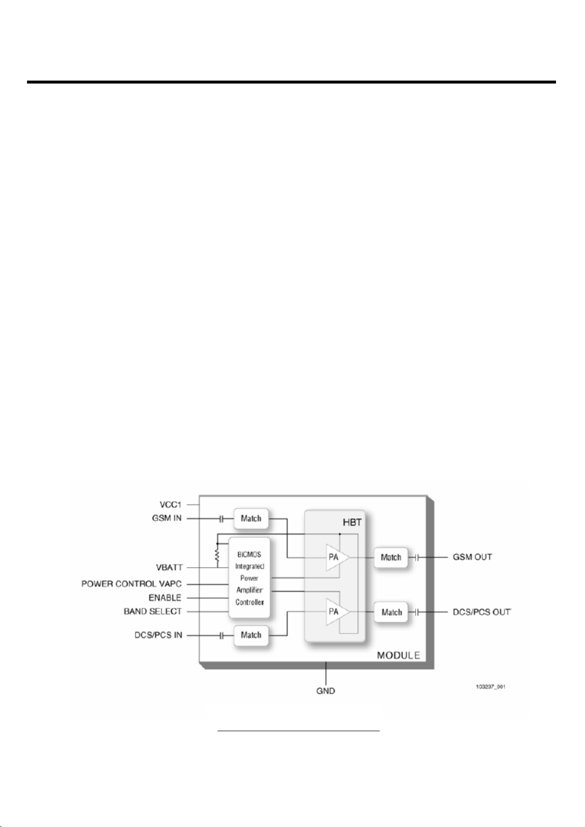
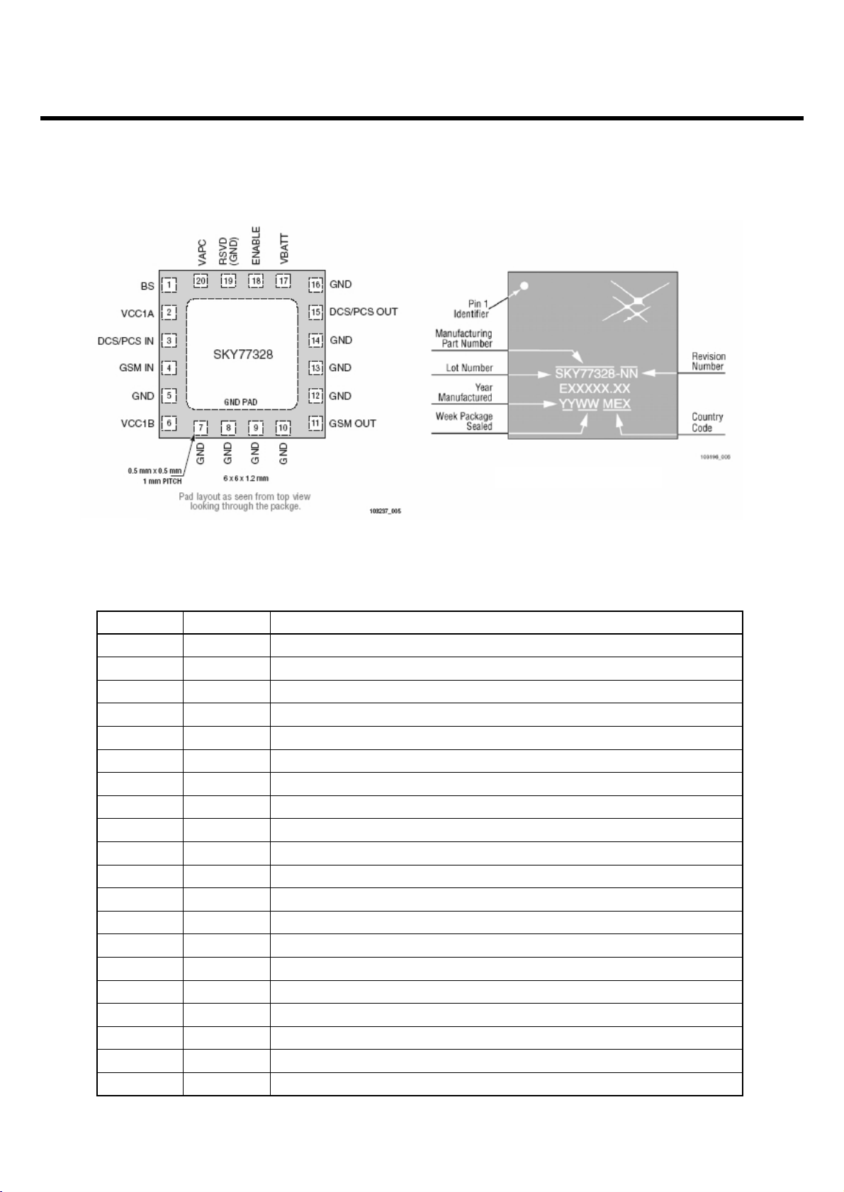
3.1 Power Transceiver (SKY77328, U500)
The SKY77328 Power Amplifier Module (PAM) is designed in a low profile (1.2 mm), compact form
factor for quad-band cellular handsets comprising GSM850/900, DCS1800, and PCS1900 operation.
The PAM also supports Class 12 General Packet Radio Service (GPRS) multi-slot operation. The
module consists of separate GSM850/900 PA and DCS1800/PCS1900 PA blocks,
impedancematching circuitry for 50 Ω input and output impedances, and a Power Amplifier Control
(PAC) block with an internal current-sense resistor. The custom BiCMOS integrated circuit provides
the internal PAC function and interface circuitry. Fabricated onto a single Gallium Arsenide (GaAs) die,
one Heterojunction Bipolar Transistor (HBT) PA block supports the GSM850/900 bands and the other
supports the DCS1800 and PCS1900 bands. Both PA blocks share common power supply pins to
distribute current. The GaAs die, the Silicon (Si) die, and the passive components are mounted on a
multi-layer laminate substrate. The assembly is encapsulated with plastic overmold. RF input and
output ports of the SKY77328 are internally matched to a 50 Ω load to reduce the number of external
components for a quad-band design. Extremely low leakage current (2.5 µA, typical) of the dual PA
module maximizes handset standby time. The SKY77328 also contains band-select switching circuitry
to select GSM (logic 0) or DCS/PCS (logic 1) as determined from the Band Select (BS) signal. In
Figure 1 below, the BS pin selects the PA output (DCS/PCS OUT or GSM850/900 OUT) and the
Analog Power Control (VAPC) controls the level of output power. The VBATT pin connects to an
internal current-sense resistor and interfaces to an integrated power amplifier control (iPAC™)
function, which is insensitive to variations in temperature, power supply, process, and input power.
The ENABLE input allows initial turn-on of PAM circuitry to minimize battery drain. Figure 1. Functional
Block Diagram
3. TECHNICAL BRIEF
Figure1. Functional Block Diagram
3. TECHNICAL BRIEF
- 16 -
SKY77328 PAM Pin Configuration-20-Pin
Leadless (Top View)
Figure 6. Typical Case Makings
Table 4. SKY77328 Pin Names and Signal Descriptions
Pin Mame Description
1BSBand Select
2 VCC1A VCC (to GSM 1st stage, DCS/PCS 1st stages, BiCMOS PAC)
3 DCS/PCS IN RF input 1710-1910 MHz (DCS1800, PCS1900)
4 GND IN RF input 824-915 MHz (GSM850/900)
5 GND RF and DC Ground
6 VCC1B RF and DC Ground
7 GND RF and DC Ground
8 GND RF and DC Ground
9 GND RF and DC Ground
10 GND RF and DC Ground
11 GSM OUT RF Output 824-915 MHz (GSM850/900)
12 GND RF and DC Ground
13 GND RF and DC Ground
14 GND RF and DC Ground
15 DCS/PCS OUT RF Output 1710-1910 MHz (DCS 1800, PCS1900)
17 VBATT Battery input to high side of intemal sense resistor
18 ENABLE BiCMOS Enable
19 RSVD(GND) RF and DC Ground
20 VAPC Power Control Bias Voltage
GMD PAD(21) GND Ground Pad, bottom

3. TECHNICAL BRIEF
- 17 -
3.2 FEM for Triband
Table 3-1 Band SW Logic Table
Figure 3- 2 FEM CIRCUIT DIAGRAM
22
GND11
GND12
23
24
GND13
4
GND2
6
GND3
GND4
7
16
GND5
GND6
17
18
GND7
GND8
19
20
GND9
14
PCS_RX1
PCS_RX2
15
VC_DCSPCS
3
VC_EGSM
9
HWXQ511
ANT
1
DCSPCS_TX
5
12
DCS_RX1
DCS_RX2
13
10
EGSM_RX1
EGSM_RX2
11
8
EGSM_TX
2
GND1
GND10
21
FL500
0R516
R518
270p
C541
0
270p
C540
ANT_SW2
ANT_SW1
Select Mode Vc(EGSM) Vc(DCS/PCS)
EGSM-Rx Low Low
EGSM-Tx High Low
DCS-Rx Low Low
PCS-Rx Low Low
DCS/PCS Low High

3. TECHNICAL BRIEF
- 18 -
3.3 26 MHz Clock (VCTCXO, X500)
The 26 MHz clock(X500) consists of a TCXO(Temperature Compensated Crystal Oscillator) which
oscillates at a frequency of 26 MHz. It is used within the SKY77328, base band
processor(AD6720,U101), Midi(U203, YMU762C-QZ) , CAMERA( U403,CL761A )
Figure 3-3. VCTCXO CIRCUIT DIAGRAM
2V75_VVCXO
3
4
C544
2.2u
OUT
VCC
X500
VCONT
GND
26MHz
1
2
C543
1000p
R521
15K
AFC

3. TECHNICAL BRIEF
- 19 -
3.4 Baseband Processor (AD6720 , U101)
• AD6720 is an ADI designed processor
• AD6720 consists of
1. Control Processor Subsystem including:
• 32-bit MCU ARM7TDMI® Control Processor
• 39 MHz operation at 1.8V
• 1Mb of on-chip System SRAM Memory
2.DSP Subsystem including:
• 16-bit Fixed Point DSP Processor
• 91 MIPS[1] at 1.8V
• Data and Program SRAM
• Program Instruction Cache
• Full Rate, Enhanced Full Rate and Half Rate
• Speech Encoding/Decoding
• Capable of Supporting AMR & PDC Speech Algorithms
3.Peripheral Functions
• Parallel and Serial Display Interface
• Keypad Interface
• Flash Memory Interface
• Page-Mode Flash Support
• 1.8V and 3.0V, 64 kbps SIM Interface
• Universal System Connector Interface
• Data Services Interface
• Battery Interface (e.g. Dallas)
4. Other
• Supports 13 MHz and 26 MHz Input Clocks
• 1.8V Typical Core Operating Voltages
• 289-Ball Package (12x12mm) , 0.65mm Ball pitch
5. The AD6720 baseband transmit section supports the following
• mobile station GMSK modulation power classes:
• GSM 900/850 power classes 4 and 5,
• DCS 1800 power classes 1 and 2, and
• PCS 1900 power classes 1 and 2

3. TECHNICAL BRIEF
- 20 -
Figure 3-4 SYSTEM INTERCONECTION OF AD6720 EXTERNAL INTERFACE
3. TECHNICAL BRIEF
- 21 -
3.4.1 Interconnection with external devices
A. RTC block interface
Countered by external X-TAL
The X-TAL oscillates 32.768KHz
B. LCD module interface
The LCD module is controlled by CAMERA IC, CL761A
If CL761A is in the state of by-pass mode, the LCD control signals from AD6720
are by-passed through CL761A.
In operating mode, the CL761A controls the LCD module through L_MAIN_LCD_CS,
L_SUB_LCD_CS, LCD_RESET, LCD_RS, LCD_WR, LCD_RD, L_DATA[15-00],
2V85_VCAM, IF_MODE, LCD_ID[1:3].
Signals Description
L_MAIN_LCD_CS MAIN LCD driver chip enable. MAIN LCD driver IC has own CS pin
LCD_ID1 Select LCD modoule maker(2.4V : SII, 0V : HyeLCD)
LCD_RESET This pin resets LCD module. This signal comes from AD6720 directly.
LCD_WR Enable writing to LCD Driver.
LCD_RD Enable reading to LCD Driver.
LCD_RS This pin determines whether the data to LCD module are display
data or control data. LCD_RS can select 16 bit parallel bus.
2V85_VCAM 2.85V voltage is supplied to LCD driver IC.
IF_MODE
Select 16bits or 8bits interface mode for MAIN LCD.
For the future
Table 3-2 . LCD CONTRON SIGNALS DISCRIPTION
3. TECHNICAL BRIEF
- 22 -
The backlight of LCD module is controlled by AD6720 via AAT3157 , U404. The control signals related
to Backlight LED are given bellow.
C. RF interface
The AD6720 control RF parts through PA_BAND, ANT_SW1, ANT_SW2, ANT_SW3 , CLKON ,
PA_EN, S_EN, S_DATA, S_CLK, RF_PWR_DWN.
Signals Description
MLED Current source for backlight LED
LCD_DIM_CTL Control LCD backlight level in 16 steps
MLED[1:2] This pins are returned-paths for backlight LED current source (MLED)
Table 3-3. DESCRIPTION OF LCD BACKLIGHT LED CONTROL
Signals Description
PA_BAND (GPO 17) PAM Band Select
ANT_SW1 (GPO 9) Antenna switch Band Select
ANT_SW2 (GPO 11) Antenna switch Band Select
RF_PWR_DWN(GPO 4) Power down Input
CLKON RF LDO Enable/Disable
PA_EN (GPO 16) PAM Enable/Disable
S_EN (GPO 19) PLL Enable/Disable
S_DATA (GPO 20) Serial Data to PLL
S_CLK (GPO 21) Clock to PLL
Table 3-4. RF CONTROL SIGNALS DESCRIPTION
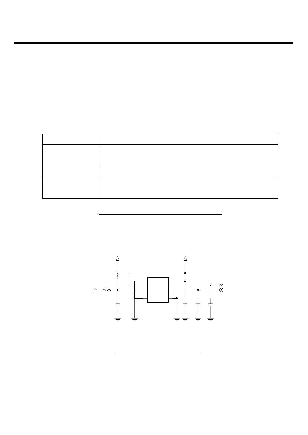
3. TECHNICAL BRIEF
- 23 -
D. SIM interface
The AD6720 provides SIM Interface Module. The AD6720 checks status periodically during
established call mode whether SIM card is inserted or not, but it doesn't check during deep Sleep
mode. In order to communicate with SIM card, 3 signals SIM_DATA, SIM_CLK,
SIM_RST(GPIO_23) are required. The descriptions about the signals are given by bellow Table 3-5
in detail.
Signals Description
SIM_DATA
This pin receives and sends data to SIM card.
This model can support only 3.0 volt interface SIM card.
SIM_CLK Clock 3.25MHz frequency.
SIM_RST
Reset SIM block
(GPIO_23)
Table 3-5. SIM CONTROL SIGNALS DESCRIPTION
Figure 3-5. SIM Interface of AD6720
SIM CONNECTOR
2V85_VSIM
89
GND4
GND5
10
IO
6
RST
2
1
VCC
5
VPP
J100
3
CLK
GND1
4
7
GND2
GND3
C128
220n 1000p
C135
NA
C133
2V85_VSIM
0R126
22p
C134
20K
R120
SIM_DATA
SIM_RST
SIM_CLK

3. TECHNICAL BRIEF
- 24 -
E. LDO Block
There are 8 LDOs in the AD6720.
- VCORE : supplies Digital baseband Processor core and AD6720 digital core
- VMEM : supplies external memory and the interface to the external memory on the digital
baseband processor (1,8V or 2.8V, 150mA)
- VEXT : supplies Radio digital interface and high voltage interface (2.8V, 170mA)
- VSIM : supplies the SIM interface circuitry on the digital processor and SIM card
(2.85V, 20mA)
- VRTC : supplies the Real-Time Clock module (1.8 V, 20µA)
- VABB : supplies the analog portions of the AD6720
- VMIC : supplies the microphone interface circuitry (2.5 V, 1 mA)
- VVCXO : supplies the voltage controlled crystal oscillator ( 2.75 V, 10 mA)
3.5 Battery Charging Block
1. It can be used to charge Lithium Ion batteries.
Charger initialization, trickle charging, and Li-Ion charging control are implemented in hardware.
2. Charging Process
- Check charger is inserted or not
- If AD6720 detects that Charger is inserted, the CC-CV charging starts.
- Exception : When battery voltage is lower than 3.2V, the precharge(low current charge mode)
starts firstly.
- And the battery voltage reach to 3.2V the CC-CV charging starts.
3. Pins used for charging
- VCHG : charger supply.
- GATEDRIVE : charge DAC output
- ISENSE : charge current sense input
- VBATSENSE : battery voltage sense input.
- BATTYPE : battery type identification input
- REFCHG : voltage reference output
4. TA (Travel Adaptor)
- Input voltage: AC 85V ~ 260V, 50~60Hz
- Output voltage: DC 5.2V ( 0.2 V )
- Output current: Max 800mA ( 50mA )
5. Battery
- Li-ion battery (Max 4.2V, Nom 3.7V)
- Standard battery: Capacity - 830mAh

3. TECHNICAL BRIEF
- 25 -
Figure 3-6. CIRCUIT FOR BATTERY CHARGING
PRE
CHARGING
NORMAL
CHARGING
VCHARGE
VBAT
R118
C127
0.1u
PRE_CHARGE_R INDLED_R
R121
1.5K
10K
R633
10
31
2
Q101
UMX1NTN
R119
1K
4
56
R632
7.5K
10K
R122
R129
VBAT
0.2
C140
1u
CUS02
G5S
4
D36D4
3
D2
D5
2
D1
D6
1
TPCF8102-TE85L-F
Q102
VCHARGE
D101
7
8
C139
4.7u
330
R131
1V8_VRTC
BATT_TEMP
C137
0.1u
R127
82KR132
C138
4.7u
2.2K
C146
0.1u
KEY_BACKLIGHT
HOOK_DET
TCK
TMS
TDO1
JTAGEN
TDI
LIGHT3
P8
GPO_22
R5
GPO_23
T12
VMEMSEL
D17
C15
C14
A13
A14
B14
T13
C12
A12
C13
B13
F17
B12
G3
F5
F2
F6
F4
REF
REFOUT
TEMP1
TEMP2
AUXADC1
AUXADC2
VRTC
VCHG
GATEDRIVE
ISENSE
VBATSENSE
REFCHG
BATTYPE
GPIO_18
GPIO19_TMS
GPIO_20
GPIO_21_TDI
JTAGEN
1uC131
1uC136
NAR138
3. TECHNICAL BRIEF
- 26 -
3.6 Display and Interface
• Main LCD
Controlled by L_MAIN_LCD_CS, LCD_RESET, LCD_RS, LCD_WR, LCD_RD, IFMODE,
L_DATA[00:15] ports
• L_MAIN_LCD_CS : MAIN LCD driver chip enable. MAIN LCD driver IC has own CS pin
• LCD_RST : This pin resets LCD module. This signal comes from AD6720 directly.
• LCD_RS: This pin determines whether the data to LCD module are display data or control data.
• L_WR : Write control Signal
• L_RD : Read control Signal. But this pin used only for debugging.
• L_DATA[00:15] : Parallel data lines.
• LCD_ID[1:2] : LCD type selection signals
- LCD_ID1 : LCD maker(2.4V is SII, 0V is HyeLCD)
- LCD_ID[2:3] : for the future using
• For using 65K color, data buses should be 16 bits.
Properties Spec. Unit
Active Screen Size 35.78*40.05*2.8 mm
Color Depth 65,536 colors
Resolution 128 X RGB X 128 dots

3. TECHNICAL BRIEF
- 27 -
Figure 3-7. LCD INTERFACE CIRCUIT
DATA13
DATA14
DATA15
_RD
DATA08
DATA09
DATA10
DATA11
DATA12
L_DATA08
L_DATA09
L_DATA10
L_DATA11
L_DATA12
L_DATA13
L_DATA14
4
6
3
INOUT_A3
INOUT_B3
7
INOUT_A2
INOUT_B2
2
8
1
INOUT_A1
INOUT_B1
9
9
1
8
INOUT_B1
INOUT_A1
2
7
INOUT_B2
INOUT_A2
3
L_DATA15
INOUT_B36INOUT_B4
INOUT_A3
INOUT_A4
4
ICVE21054E250R401FR
G2
10
G1
5
FL603
C_CD00
C_CD01
4
ICVE21184E150R500FR
5
G1
INOUT_A3
INOUT_A4
10
G2
INOUT_B3
INOUT_B4
6
FL605
C_CD02
3
INOUT_A2
INOUT_B2
7
2
8
C_CD03
1
INOUT_A1
INOUT_B1
9
C_CD06
C_CD04
C_CD05
C_CD07
9
8
7
6
ICVE21184E150R500FRFL607
G2
INOUT_B1
INOUT_B2
INOUT_B3
INOUT_B4
10
G1
5
INOUT_A1
INOUT_A2
INOUT_A3
INOUT_A4
1
2
3
4
NAR609
NAR619
NAR613
NAR617
NAR605
R607 NA
R618 NA
R611 NA
R615 NA
FL601ICVE21054E250R401FR
5
G1
INOUT_A4
10
G2
INOUT_B4
100K
R640
VGA CAMERA
128x128LCD CONNECTOR
2V85_VCAM
NAR606
NAR610
NAR603
NAR601
NAR602
R604 NA
ADD01
R612 NA
R608 NA
_WR
DATA00
DATA01
DATA02
DATA03
DATA04
_LCD_CS
R600 NA
NAR614
DATA05
R616 NA
DATA06
2V8_C_PWR
DATA07
CN600
2
3
4
FL600
5
G1
INOUT_A2
INOUT_A3
INOUT_A4
10
G2
INOUT_B2
INOUT_B3
INOUT_B4
6
8
7
ICVE21054E250R401FR
L_DATA02
L_DATA01
L_DATA00
60
1
1
INOUT_A1
INOUT_B1
9
L_DATA03
LCD_RD
MOTOR
MLED1
MLED2
R624 0
464748
8
INOUT_B1
INOUT_A1
2
7
INOUT_B2
INOUT_A2
3
6
6
INOUT_B3
INOUT_A3
4
INOUT_B4
INOUT_A4
789
G2
10
G1
5
FL602
495505152535455565758
10111213141516
R625 100K
LCD_MAKER(TO GPIO_17)
LCD_ID1
ICVE21054E250R401FR
100
R626
R627
45
1718192202122232425262728
MLED
BACK_BATT
FL604
1
2
3
4
5
G1
ICVE21184E150R500FR
INOUT_A4
INOUT_A1
INOUT_A2
INOUT_A3
10
G2
INOUT_B1
INOUT_B2
INOUT_B3
INOUT_B4
9
8
7
6
C600
22p
100K
9
1
8
INOUT_B1
INOUT_A1
2
R641
C_MCLK
7
INOUT_B2
INOUT_A2
3
C_PCLK
29330
SPK_RCV_P
6
INOUT_B3
INOUT_B4
INOUT_A3
INOUT_A4
4
0
C_VS
C_HS
31323334353637383944041424344
1uC604
39pC602
SPK_RCV_N
2V8_C_PWR
FL606
ICVE21184E150R500FR
G2
10
G1
5
C641
NA
C603 0.1u
C601 39p
R630 4.7K
4.7KR629
FL608
ICVE21184E150R500FR
9
INOUT_B1
INOUT_A1
1
C_SDA
8
2
7
INOUT_B2
INOUT_A2
3
C_SCK
6
INOUT_B3
INOUT_A3
4
C_RST
INOUT_B4
INOUT_A4
G2
10
G1
5
59
9
1
LCD_RESET
L_DATA07
L_DATA06
L_DATA05
L_DATA04
LCD_WR
LCD_RS
L_MAIN_LCD_CS
3. TECHNICAL BRIEF
- 28 -
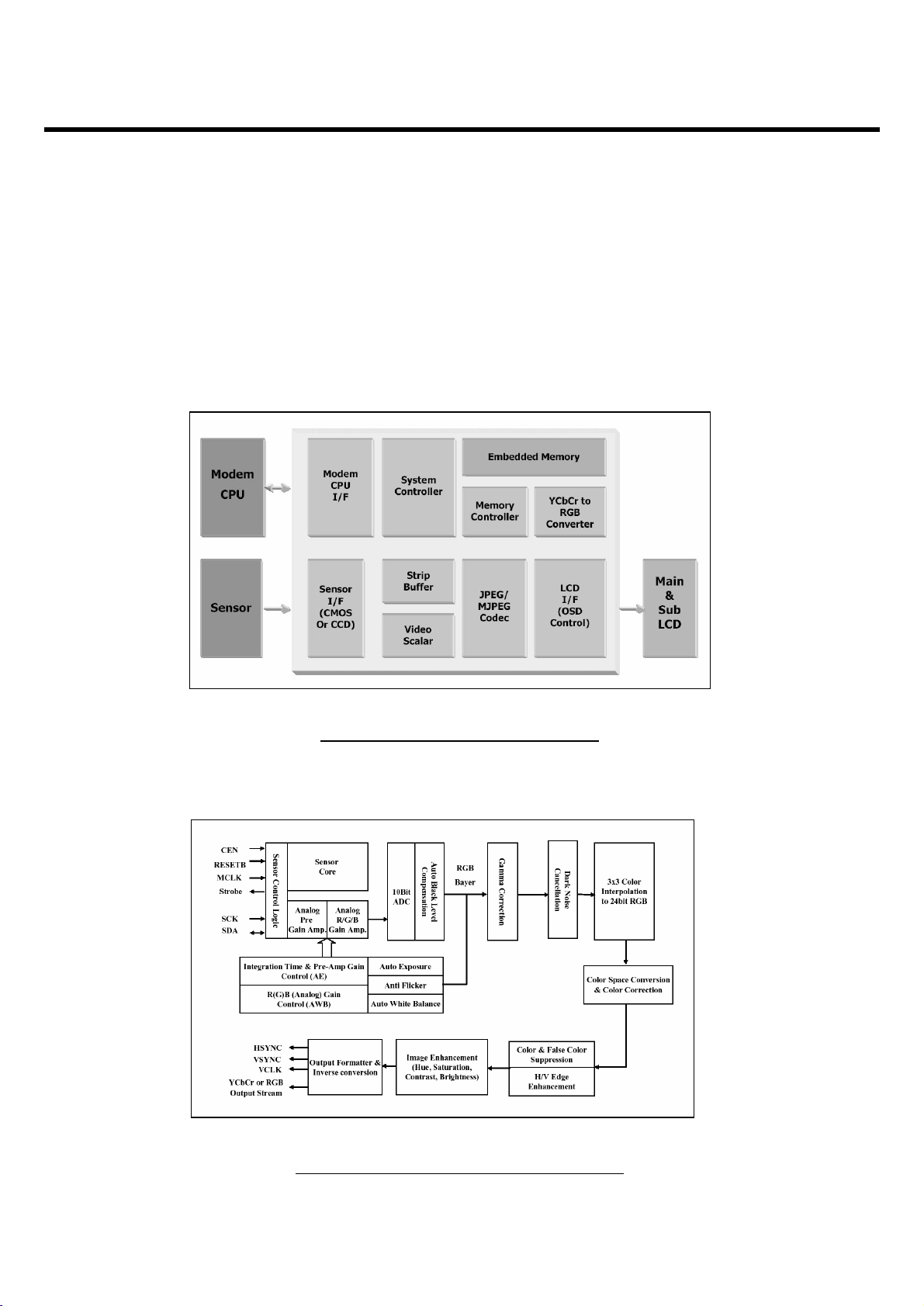
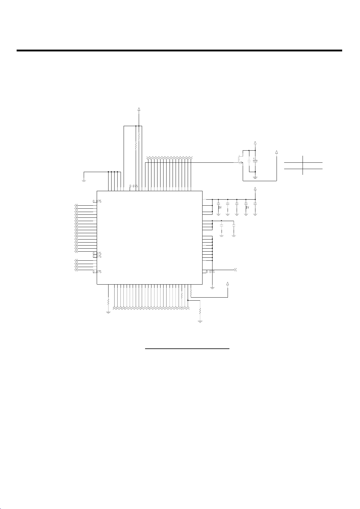
3.7 Camera IC(CL761A , U403)
This model has a built-in VGA(640 x 480) camera module. And the camera produces JPG pictures.
Camera module is controlled by CL761A. Interface is done by I2C and YCbCr format. I2C is a control
signal and YCbCr is real data interface signal.
Figure 3-8. CL761A BLOCK DIAGRAM
Figure 3-9. SENSOR CHIP BLOCK DIAGRAM
3. TECHNICAL BRIEF
- 29 -
Figure 3-10. CL761A CIRCUIT
(USC6)
CAMERA CTL IC
STATUS
1608
DEACTIVE
ACTIVE
C_PWDN
HIGH
LOW
R417
100K
2V85_VCAM
C412
1u
2V85_VCAM
Q401
D
G
S
SI1305-E3
C416
0.01u
TEST_EN
L6
M7
T_MODE0
VDDC1
A8
VDDC2
A10
VDDC3
D2
VDDC4
H10
B9
VDDI1
C7
VDDI2
VDDL
J2
K5
VDDS
XIN
A2
A1
XOUT
D3
M_SD11
M_SD12
C2
B1
M_SD13E3M_SD14C1M_SD15
M_SD2A6M_SD3B6M_SD4C6M_SD5A4M_SD6B4M_SD7
C4
C3
M_SD8B3M_SD9
F3
M_WR_N
SCAN_EN
M6
STROBE
G2
K1
L_RD_N
L_RESET_N
L2
L_WR_N
K2
A9
MS_CS_N
D9
M_8BIT
M_ADS
C8
M_CS_N
E2
F1
M_HOLD
E1
M_INTR
D1
M_RD_NG3M_RESET_N
M_SA0D8M_SA1
B10
B7
M_SD0A7M_SD1
A3
M_SD10
L_DA10
F10
L_DA11
E10
F9
L_DA12
L_DA13
D10
E9
L_DA14
L_DA15
C10
L_DA16
H2
G1
L_DA17
L_DA2
K10
L_DA3
H8
H9
L_DA4
L_DA5
J10
L_DA6
G10
G9
L_DA7
L_DA8
G8
L_DA9
F8
B5
GNDC2
C5
GNDC3
GNDC4
F2
L5
GNDC5
GNDI1
B2
GNDI2
E8
J3
GNDI3
GNDI4
K6
J1
GPIO_0H3GPIO_1H1GPIO_2
K9
LS_CS_N
K3
L_ADS
L1
L_CS_N
L_DA0
L10
J9
L_DA1
K7
C_D1
C_D2M8C_D3L8C_D4
K8
M9
C_D5L9C_D6
C_D7
J8
C_HS
K4
M1
C_MCLK
C_PCLK
L4
L3
C_PWDN
M3
C_RST
M5
C_SCK
C_SDA
M4
C_VS
M2
A5
GNDC1
U403
EUSY0240501
CIS_TYPE0
M10
C9
CIS_TYPE1
CIS_TYPE2
B8
L7
C_D0
2V85_VCAM
R407
0.1u
C410
100K
R408
100K
100K
R414
0.01u
C411
C415
4.7u
C413
1u
R415
0
2V8_C_PWR
2V85_VCAM
C414
1u
C409
0.1u 10u
C408
0
R416
CAM_INT
_WR
26M_CAM
L_MAIN_LCD_CS
DATA01
DATA10
DATA11
DATA12
DATA13
DATA14
DATA15
DATA02
DATA03
DATA04
DATA05
DATA06
DATA07
DATA08
DATA09
L_DATA03
L_DATA04
L_DATA05
L_DATA06
L_DATA07
L_DATA08
L_DATA09
LCD_RD
LCD_WR
ADD01
_LCD_CS
CAM_HOLD
_RD
CAM_RST
ADD01
ADD02
DATA00
C_SCK
C_SDA
C_VS
LCD_RS
L_DATA00
L_DATA01
L_DATA10
L_DATA11
L_DATA12
L_DATA13
L_DATA14
L_DATA15
L_DATA02
C_CD00
C_CD01
C_CD02
C_CD03
C_CD04
C_CD05
C_CD06
C_CD07
C_HS
C_MCLK
C_PCLK
C_RST
3. TECHNICAL BRIEF
- 30 -
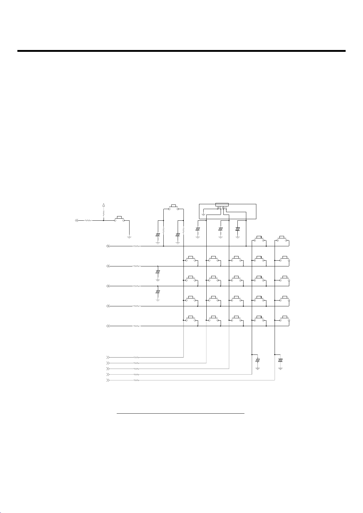
3.8 Keypad Switches and Scanning
The key switches are metal domes, which make contact between two concentric pads on the keypad
layer of the PCB when pressed. There are 26 switches (Normal Key 24EA, Volume up down side key),
connected in a matrix of 5 rows by 5 columns and additional GPIO 35 for KEY_ROW5, as shown in
Figure 3-11, except for the power switch (KB1), which is connected independently. Functions, the row
and column lines of the keypad are connected to ports of AD6720. The columns are outputs, while the
rows are inputs and have pull-up resistors built in. When a key is pressed, the corresponding row and
column are connected together, causing the row input to go low and generate an interrupt. The
columns/rows are then scanned by AD6720 to identify the pressed key.
Figure 3-11. Keypad Switches and Scanning
VOL_UP
VOL_DOWN
123
4
CN601
VA302
SW308
SW313
SW318
SW323
0
2
87
EVL14K02200
SW309
SW324
EVL14K02200
1
45
VA303
#
EVL14K02200
3
6
9
CLR
SW305
SW315
SW320
SW325
LEFT
UP
RIGHT
DOWN
FAV
SW306
SW311
SW316SW314
SW321
SW326
MENU
SEL
SEND
CONF
POWERKEY
680R301
KEY_ROW0
KEY_ROW1
KEY_ROW2
KEY_ROW3
KEY_ROW4
VBAT
R300
10K
SW304
END
R324 680
R326
R336
SW300
T
R302
100
EVL14K02200
VA306
EVL14K02200
VA307
EVL14K02200
VA305
VA304
680R320
680
680R331
680
VA301
R303
100
EVL14K02200
SW307 SW310
SW312
SW317 SW319
SW322
*
KEY_COL0
KEY_COL1
KEY_COL2
KEY_COL3
KEY_COL4
680R339
R341 680
680R342
R343
680
680R344
VA312
EVL14K02200
VA313
EVL14K02200
3. TECHNICAL BRIEF
- 31 -
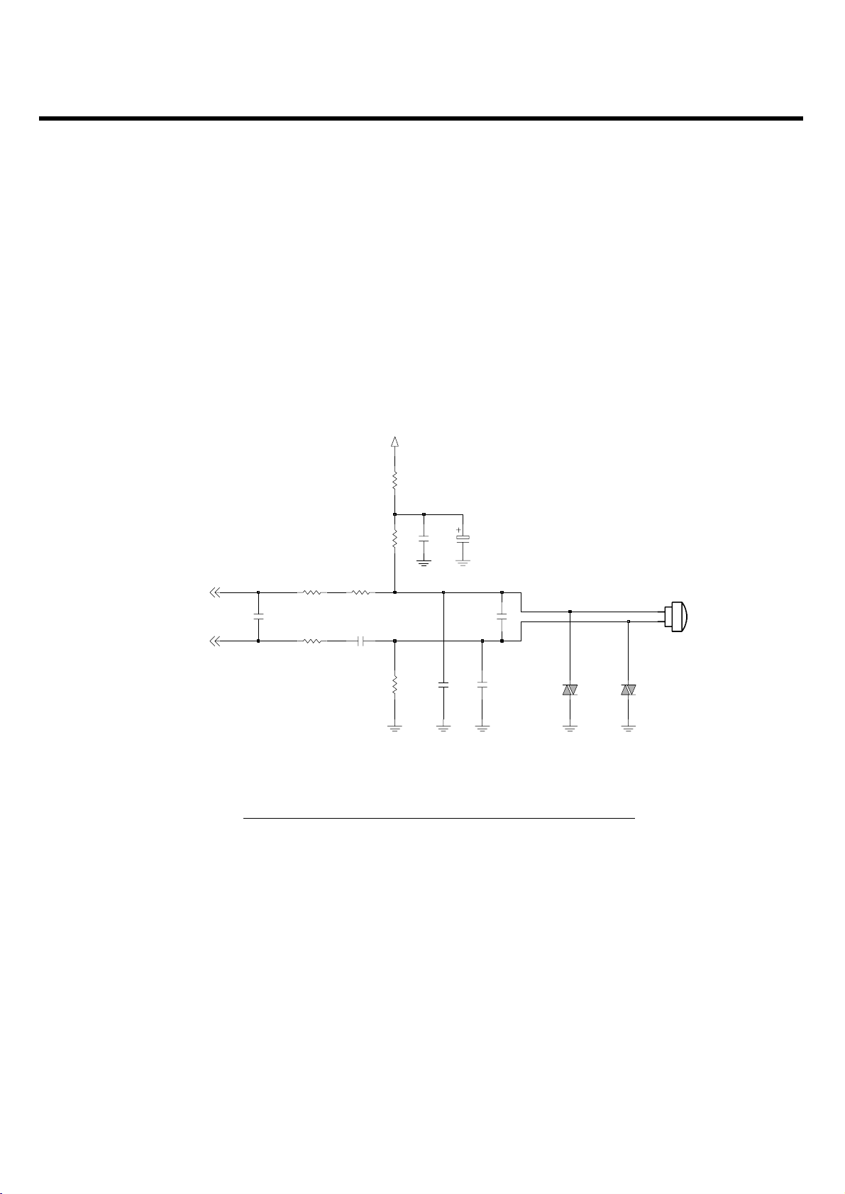
3.9 Microphone
The microphone is placed to the front cover and contacted to main PCB. The audio signal is passed to
AIN1P and AININ pins of AD6720. The voltage supply VMIC is output from AD6720, and is a biased
voltage for the AIN1P. The AIN1P and AIN1N signals are then A/D converted by the voiceband ADC
part of AD6720.The digitized speech (PCM 8KHz ,16KHz) is then passed to the DSP section of
AD6720 for processing (coding, interleaving etc).
Figure 3-12. Connection between Microphone and AD6535
CLOSE TO MIC
2V5_VMIC
VA205
EVL5M02200
0R217
EVL5M02200
VA206
C226 39p
10u
C215
1K
R213
100R216
2.2K
R215
C223
0.1u
C221
39p
C219
39p
R219 100
2.2K
R220
39pC225
1
2
MIC200
OB4-15L42-C33L
C220
39p
VINNORN
VINNORP
 Loading...