

Page 1
Date: May, 2008 / Issue 1.0
Service Manual
Model : KF755d
Service Manual
KF755d
Internal Use Only
Page 2

- 3 -
1. INTRODUCTION .............................. 5
1.1 Purpose................................................... 5
1.2 Regulatory Information............................ 5
2. PERFORMANCE...............................7
2.1 System Overview .....................................7
2.2 Usable environment .................................8
2.3 Radio Performance ..................................9
2.4 Current Consumption.............................18
2.5 RSSI.......................................................18
2.6 Battery Bar .............................................18
2.7 Sound Pressure Level............................19
2.8 Charging ................................................20
3. TECHNICAL BRIEF ........................21
3.1 Digital Baseband(DBB) & Multimedia
Processor...............................................21
3.2 GAM Hardware Subsystem ...................45
3.3 Audio Part ..............................................57
3.4 GPADC(General Purpose ADC) and
AUTOADC2 ...........................................65
3.5 Charger control ......................................66
3.6 Voltage Regulation.................................72
3.7 RF Technical Description.......................73
4. TROUBLE SHOOTING ...................84
4.1 Power ON Trouble .................................84
4.2 USB Trouble ..........................................85
4.3 SIM Detect Trouble ................................86
4.4 MicroSD card Trouble ............................87
4.5 Keypad, Touch Button and
Touch Screen Trouble ...........................88
4.6 Multi EL lighting Trouble ........................93
4.7 Camera Trouble .....................................97
4.8 Main LCD Trouble................................103
4.9 Keypad Backlight Trouble ....................105
4.10 Folder ON/OFF Trouble .....................107
4.11 Audio Trouble Shooting .....................109
4.12 Charger Trouble Shooting..................128
4.13 Checking Bluetooth Block ..................131
4.14 RF Component...................................138
4.15 Procedure to check ............................139
4.16 Checking Common Power
Source Block......................................140
4.17 Checking VCXO Block .......................145
4.18 Checking Front End Module Block.....150
4.19 Checking Front End Module
Block input logic .................................151
4.20 Checking WCDMA Block ...................154
4.21 Checking GSM Block .........................169
5. DOWNLOAD .................................184
5.1 LGDP2 .................................................184
5.2 Download .............................................186
6. BLOCK DIAGRAM ........................188
7. Circuit Diagram ............................191
8. BGM Pin Map................................203
9. PCB LAYOUT................................209
10. Calibration & RF Auto Test
Program (Hot Kimchi)................219
10.1 General Description ...........................219
10.2 XCALMON Environment ....................219
10.3 Calibration Environment.....................220
10.4 Program Operation ............................221
11. Stand-alone Test ........................226
11.1 General Description ...........................226
11.2 Program Operation ............................227
11.3 Stand-alone Test................................230
12. EXPLODED VIEW &
REPLACEMENT PART LIST ......233
12.1 EXPLODED VIEW .............................233
12.2 Replacement Parts ............................235
12.3 Accessory ..........................................256
Table Of Contents
LGE Internal Use Only
Copyright © 2008 LG Electronics. Inc. All right reserved.
Only for training and service purposes
Page 3

- 4 -
LGE Internal Use Only
Copyright © 2008 LG Electronics. Inc. All right reserved.
Only for training and service purposes
Page 4

LGE Internal Use Only
Copyright © 2008 LG Electronics. Inc. All right reserved.
Only for training and service purposes
- 5 -
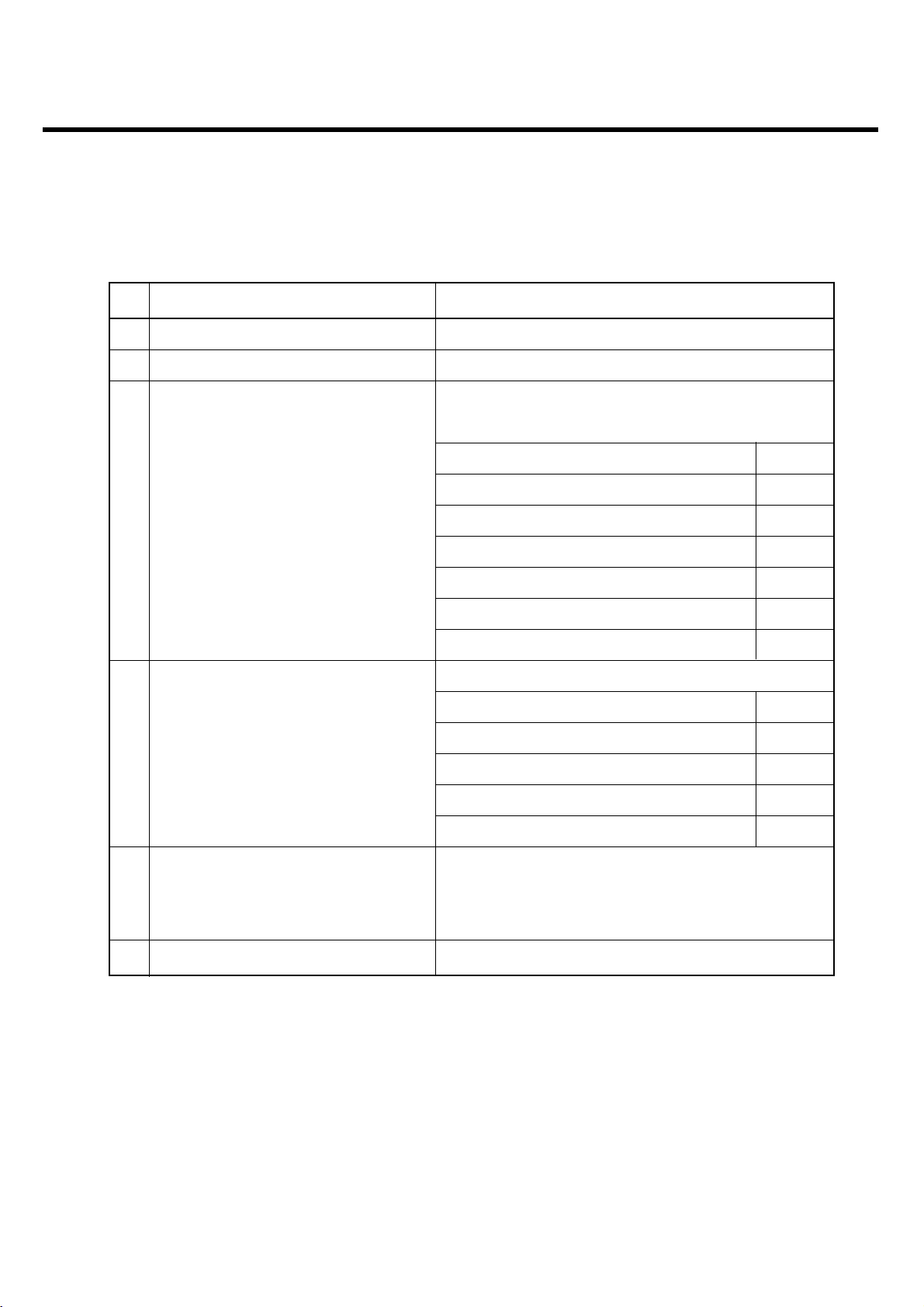
1.1 Purpose
This manual provides the information necessary to repair, calibration, description and download the
features of this model.
1.2 Regulatory Information
A. Security
Toll fraud, the unauthorized use of telecommunications system by an unauthorized part (for example,
persons other than your company’s employees, agents, subcontractors, or person working on your
company’s behalf) can result in substantial additional charges for your telecommunications services.
System users are responsible for the security of own system.
There are may be risks of toll fraud associated with your telecommunications system. System users
are responsible for programming and configuring the equipment to prevent unauthorized use. The
manufacturer does not warrant that this product is immune from the above case but will prevent
unauthorized use of commoncarrier telecommunication service of facilities accessed through or
connected to it. The manufacturer will not be responsible for any charges that result from such
unauthorized use.
B. Incidence of Harm
If a telephone company determines that the equipment provided to customer is faulty and possibly
causing harm or interruption in service to the telephone network, it should disconnect telephone
service until repair can be done. A telephone company may temporarily disconnect service as long as
repair is not done.
C. Changes in Service
A local telephone company may make changes in its communications facilities or procedure. If these
changes could reasonably be expected to affect the use of the phones or compatibility with the net
work, the telephone company is required to give advanced written notice to the user, allowing the user
to take appropriate steps to maintain telephone service.
D. Maintenance Limitations
Maintenance limitations on the phones must be performed only by the manufacturer or its authorized
agent. The user may not make any changes and/or repairs expect as specifically noted in this manual.
Therefore, note that unauthorized alternations or repair may affect the regulatory status of the system
and may void any remaining warranty.
1. INTRODUCTION
1. INTRODUCTION
Page 5

LGE Internal Use Only
Copyright © 2008 LG Electronics. Inc. All right reserved.
Only for training and service purposes
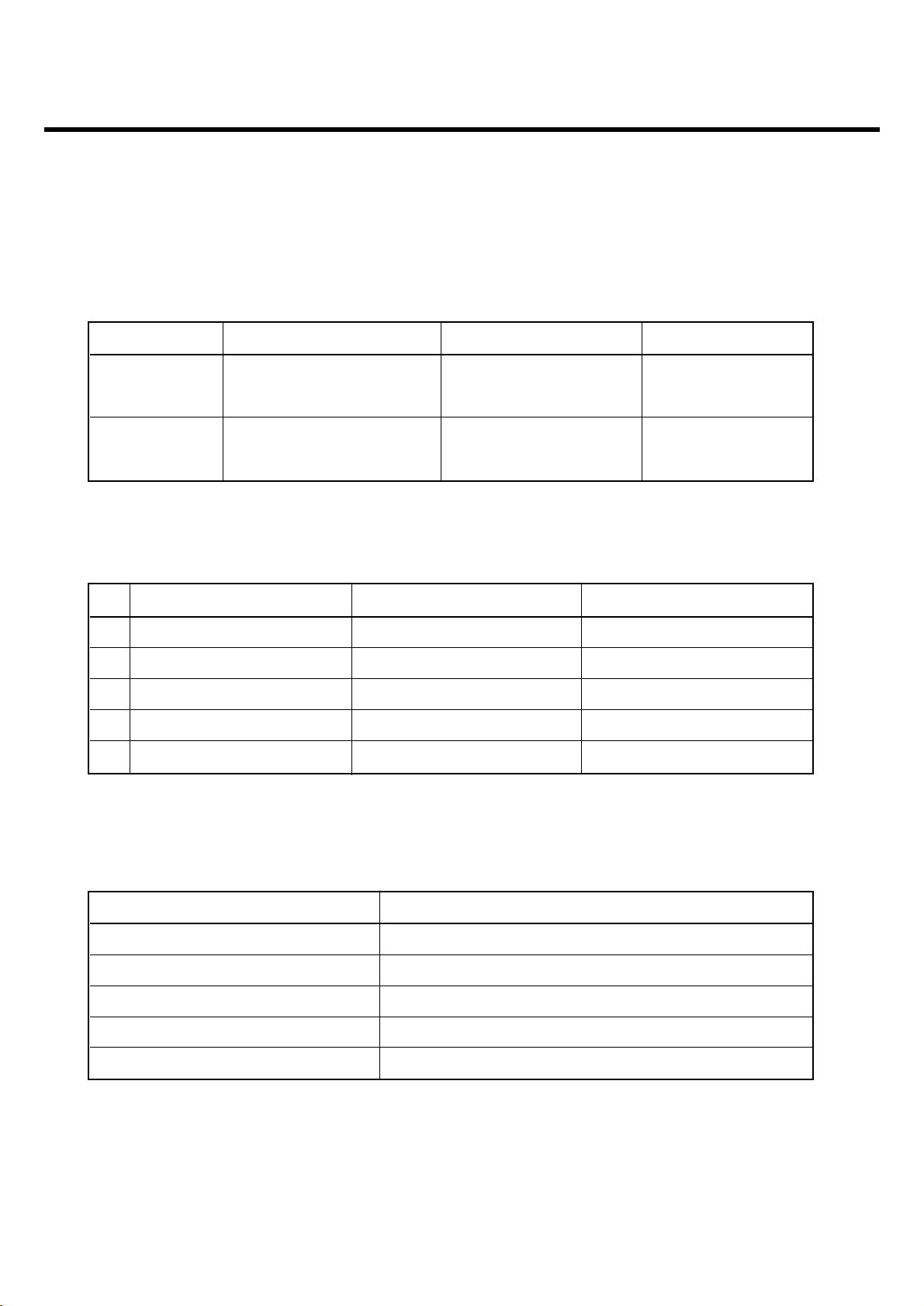
E. Notice of Radiated Emissions
This model complies with rules regarding radiation and radio frequency emission as defined by local
regulatory agencies. In accordance with these agencies, you may be required to provide information
such as the following to the end user.
F. Pictures
The pictures in this manual are for illustrative purposes only; your actual hardware may look slightly
different.
G. Interference and Attenuation
A phone may interfere with sensitive laboratory equipment, medical equipment, etc. Interference from
unsuppressed engines or electric motors may cause problems.
H. Electrostatic Sensitive Devices
ATTENTION
Boards, which contain Electrostatic Sensitive Device (ESD), are indicated by the sign.
Following information is ESD handling:
• Service personnel should ground themselves by using a wrist strap when exchange system boards.
• When repairs are made to a system board, they should spread the floor with anti-static mat which is
also grounded.
• Use a suitable, grounded soldering iron.
• Keep sensitive parts in these protective packages until these are used.
• When returning system boards or parts like EEPROM to the factory, use the protective package as
described.
1. INTRODUCTION
- 6 -
Page 6
LGE Internal Use Only
Copyright © 2008 LG Electronics. Inc. All right reserved.
Only for training and service purposes
2. PERFORMANCE
- 7 -
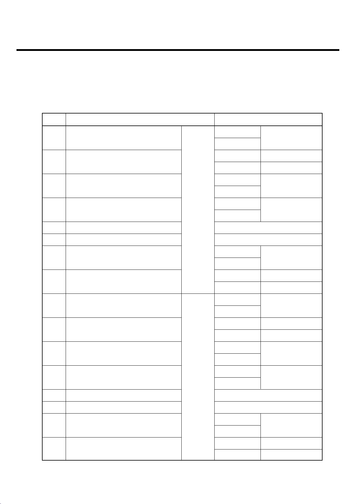
2.1 System Overview
2. PERFORMANCE
Item Specification
Shape GSM900/1800/1900 & WCDMA Slide type - Dual Mode Handset
Size 50.8X102.8X11.8 mm
Weight 116g (with standard battery)
Power 800mAh Li-Ion
Talk Time Over 170 Min (WCDMA, Tx=12 dBm, Voice)
Over 190 Min (GSM, Tx=Max, Voice)
Standby Time Over 220 hrs (WCDMA, DRX=2.56)
Over 220 hrs (GSM, Paging period=5)
Antenna Intenna type
Main LCD 2.4"(320x240), 260K TFT Color LCDs
Main LCD BL White LED Backlight
Vibrator Yes (Coin Type)
Speaker Yes
MIC Yes (SMD Type)
Receiver Yes
Earphone Jack Yes
SIM Socket Yes(SIM Block Type) : 3.0V & 1.8V
Volume Key Push Type ( + , - )
Voice Key Push Type
External Memory T - Flash Socket
I/O Connect 18 Pin
Page 7

LGE Internal Use Only
Copyright © 2008 LG Electronics. Inc. All right reserved.
Only for training and service purposes
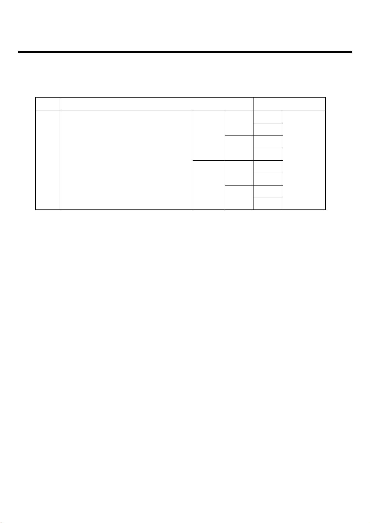
2.2 Usable environment
1) Environment
2) Environment (Accessory)
* CLA : 12~24V(DC).
2. PERFORMANCE
- 8 -
Item Specification Unit
Voltage 3.7 (Typ), 3.4 (Min), (Shut Down: 3.23) V
Operation Temp -20 ~ + 60 °C
Storage Temp -30 ~ + 85 °C
Humidity max. 85 %
Item Spec. Min Typ. Max Unit
Power Available power 100 220 240 Vac
Page 8
LGE Internal Use Only
Copyright © 2008 LG Electronics. Inc. All right reserved.
Only for training and service purposes
2. PERFORMANCE
- 9 -
2.3 Radio Performance
1) Transmitter-GSM Mode
No Item GSM DCS/PCS
1 Conducted MS allocated 100k~1GHz -39dBm 9k~1GHz -39dBm
Spurious Channel 1G~1710MHz -33dBm
Emission 1G~12.75GHz -33dBm 1710M~1785MHz -39dBm
1785M~12.75GHz -33dBm
Idle Mode 100k~880MHz -60dBm 100k~880MHz -60dBm
880M~915MHz -62dBm 880M~915MHz -62dBm
915M~1000Mz -60dBm 915M~1000MHz -60dBm
1G~1.71GHz -50dBm 1G~1.71GHz -50dBm
1.71G~1.785GHz -56dBm 1.71G~1.785GHz -56dBm
1.785G~12.75GHz -50dBm 1.785G~12.75GHz -50dBm
Radiated MS allocated 30M~1GHz -36dBm 30M~1GHz -36dBm
Spurious Channel 1G~1710MHz -30dBm
Emission 1G~4GHz -30dBm 1710M~1785MHz -36dBm
1785M~4GHz -30dBm
Idle Mode 30M ~ 880MHz -57dBm 30M~880MHz -57dBm
880M ~ 915MHz -59dBm 880M~915MHz -59dBm
915M~1GHz -57dBm 915M~1GHz -57dBm
1G~1.71GHz -47dBm 1G 1.71GHz -47dBm
1.71G~1.785GHz -53dBm 1.71G~1.785GHz -53dBm
1.785G~4GHz -47dBm 1.785G~4GHz -47dBm
Page 9
LGE Internal Use Only
Copyright © 2008 LG Electronics. Inc. All right reserved.
Only for training and service purposes
2. PERFORMANCE
- 10 -
No Item GSM DCS/PCS
2 Frequency Error ± 0.1ppm ± 0.1ppm
3 Phase Error ± 5(RMS) ± 5(RMS)
± 20(PEAK) ± 20(PEAK)
4 Frequency Error 3dB below reference sensitivity 3dB below reference sensitivity
Under Multipath and RA250 : ± 200Hz RA250: ± 250Hz
Interference Condition HT100 : ± 100Hz HT100: ± 250Hz
TU50 : ± 100Hz TU50: ± 150Hz
TU3 : ± 150Hz TU1.5: ± 200Hz
5 Output RF Due to 0 ~ 100kHz +0.5dB 0 ~ 100kHz +0.5dB
Spectrum modulation 200kHz -30dB 200kHz -30dB
250kHz -33dB 250kHz -33dB
400kHz -60dB 400kHz -60dB
600 ~ 1800kHz -66dB 600 ~ 1800kHz -60dB
1800 ~ 3000kHz -69dB 1800 ~ 6000kHz -65dB
3000 ~ 6000kHz -71dB ≥ 6000kHz -73dB
≥ 6000kHz -77dB
Due to 400kHz -19dB 400kHz -22dB
Switching 600kHz -21dB 600kHz -24dB
transient 1200kHz -21dB 1200kHz -24dB
1800kHz -24dB 1800kHz -27dB
7 Intermodulation attenuation - Frequency offset 800kHz
Intermodulation product should
be Less than 55dB below the
level of Wanted signal
Page 10

No Item GSM DCS/PCS
8 Transmitter Output Power Level Power Toler. Level Power Toler.
533 ±3030 ±3
631 ±3128 ±3
729 ±3226 ±3
827 ±3324 ±3
925 ±3422 ±3
10 23 ±3 5 20 ±3
11 21 ±3 6 18 ±3
12 19 ±3 7 16 ±3
13 17 ±3 8 14 ±3
14 15 ±3 9 12 ±4
15 13 ±3 10 10 ±4
16 11 ±5 11 8 ±4
17 9 ±5 12 6 ±4
18 7 ±5 13 4 ±4
19 5 ±5 14 2 ±5
15 0 ±5
9 Burst timing Mask IN Mask IN
LGE Internal Use Only
Copyright © 2008 LG Electronics. Inc. All right reserved.
Only for training and service purposes
2. PERFORMANCE
- 11 -
Page 11
LGE Internal Use Only
Copyright © 2008 LG Electronics. Inc. All right reserved.
Only for training and service purposes
2. PERFORMANCE
- 12 -
2) Transmitter-WCDMA Mode
No Item Specification
1 Maximum Output Power Class 3 : +24dBm(+1/-3dB)
Class4: +21dBm(±2dB)
2 Frequency Error ± 0.1ppm
3 Open Loop Power control in uplink ± 9dB@normal, ± 12dB@extreme
4 Inner Loop Power control in uplink Adjust output(TPC command)
cmd 1dB 2dB 3dB
+1 +0.5/1.5 +1/3 +1.5/4.5
0 -0.5/+0.5 -0.5/+0.5 -0.5/+0.5
-1 -0.5/-1.5 -1/-3 -1.5/-4.5
Group (10 equel command group)
+1 +8/+12 +
5 Minimum Output Power -50dBm(3.84MHz)
6 Out-of-synchronization handling of output power Qin/Qout : PCCH quality levels
Toff@DPCCH/Ior : -22 -> -28dB
Ton@DPCCH/Ior : -24 -> -18dB
7 Transmit OFF Power -56dBm(3.84MHz)
8 Transmit ON/OFF Time Mask ± 25us
PRACH,CPCH,uplinlk compressed mode
9 Change of TFC ± 25us
Power varies according to the data rate DTX :
DPCH off (minimize interference between UE)
10 Power setting in uplink compressed ± 3dB(after 14slots transmission gap)
11 Occupied Bandwidth(OBW) 5MHz(99%)
12 Spectrum emission Mask -35-15*(∆f-2.5)dBc@∆f=2.5~3.5MHz,30k
-35-1*(∆f-3.5)dBc@∆f=3.5~7.5MHz,1M -39-
10*(∆f-7.5)dBc@∆f=7.5~8.5MHz,1M
-49dBc@∆f=8.5~12.5MHz,1M
13 Adjacent Channel Leakage Ratio(ACLR) 33dB@5MHz, ACP>-50dBm
43dB@10MHz, ACP>-50dBm
Page 12
LGE Internal Use Only
Copyright © 2008 LG Electronics. Inc. All right reserved.
Only for training and service purposes
2. PERFORMANCE
- 13 -
No Item Specification
14 Spurious Emissions (*: additional requirement) -36dBm@f=9~150KHz, 1K BW -
-36dBm@f=150KHz~30MHz, 10k
-36dBm@f=30~1000MHz, 100k
-30dBm@f=1~12.75GHz, 1M
-41dBm*@1893.5~1919.6MHz, 300k
-67dBm*@925~935MHz, 100k
-79dBm*@935~960MHz, 100k
-71dBm*@1805~1880MHz, 100k
15 Transmit Intermodulation -31dBc@5MHz, Interferer -40dBc
-41dBc@10MHz, Interferer -40dBc
16 Error Vector Magnitude (EVM) 17.5%(>-20dBm)
(@12.2K, 1DPDCH+1DPCCH)
17 Transmit OFF Power -15dB@SF=4, 768kbps,
multi-code transmission
Page 13
- 14 -
2. PERFORMANCE
3)Receiver-GSM Mode
LGE Internal Use Only
Copyright © 2008 LG Electronics. Inc. All right reserved.
Only for training and service purposes
No Item GSM850/900 DCS & PCS
1 Sensitivity (TCH/FS Class II) -105dBm -105dBm
2 Co-Channel Rejection (TCH/FS C/Ic=7dB C/Ic=7dB
Class II, RBER, TU high/FH)
3 Adjacent 200kHz C/Ia1=-12dB C/Ia1=-12dB
Channel
Rejection 400kHz C/Ia2=-44dB C/Ia2=-44dB
4 Intermodulation Rejection Wanted Signal: -98dBm Wanted Signal :-96dBm 1st
1’st interferer: -44dBm 1’st interferer: -44dBm
2’st interferer: -45dBm 2’st interferer: -44dBm
5 Blocking Response Wanted Signal: -101dBm Wanted Signal: -101dBm
(TCH/FS Class II, RBER) Unwanted Signal: Unwanted Signal:
Depend on freq. Depend on freq.
Page 14

- 15 -
2. PERFORMANCE
4) Receiver-WCDMA Mode
LGE Internal Use Only
Copyright © 2008 LG Electronics. Inc. All right reserved.
Only for training and service purposes
No Item Specification
1 Reference Sensitivity Level -106.7dBm(3.84M)
2 Maximum Input Level -25dBm(3.84MHz)
-44dBm/3.84MHz(DPCH_Ec)
UE@+20dBm output power(class3)
3 Adjacent Channel Selectivity (ACS) 33dB
UE@+20dBm output power(class3)
4In-band Blocking -56dBm/3.84MHz@10MHz
UE@+20dBm output power(class3)
-44dBm/3.84MHz@15MHz
UE@+20dBm output power(class3)
5 Out-band Blocking -44dBm/3.84MHz@f=2050~2095 &
2185~2230MHz, band a)
UE@+20dBm output power(class3)
-30dBm/3.84MHz@f=2025~2050 &
2230~2255MHz, band a)
UE@+20dBm output power(class3)
-15dBm/3.84MHz@f=1~2025 &
2255~12500MHz, band a)
UE@+20dBm output power(class3)
6 Spurious Response -44dBm CW
UE@+20dBm output power(class3)
7 Intermodulation Characteristic -46dBm CW@10MHz &
-46dBm/3.84MHz@20MHz
UE@+20dBm output power(class3)
-57dBm@f=9KHz~1GHz, 100k BW
8 Spurious Emissions -47dBm@f=1~12.75GHz, 1M
-60dBm@f=1920~1980MHz, 3.84MHz
-60dBm@f=2110~2170MHz, 3.84MHz
Page 15
- 16 -
2. PERFORMANCE
5) Transmitter
5.1 Transmitter
LGE Internal Use Only
Copyright © 2008 LG Electronics. Inc. All right reserved.
Only for training and service purposes
No Item Specification
1 Out Power Class 2 : -6~4dBm
2 Power Density Power density < 20dBm per 100kHz EIRP
3 Power Control Option
2dB ≤ step size ≤ 8dB
4 TX Output Spectrum -Frequency range fmax & fmin @ below the level of -30dBm
(100khz BW) within 2.4GHz~2.4835GHz
5 TX Output Spectrum -20dB Bandwidth ≤ 1MHz
6 Tx Output Spectrum -Adjacent channel Po ≤ -20dBm @ C/I = 2MHz
≤ -40dBm @ C/I ≥ 3MHz
7 Modulation Characteristics 140kHz ≤ delta f1 avg ≤ 175kHz
delta f2max ≥ 115kHz at least 99.9% of all
deltaf2max delta f2avg/deata f1avg ≥ 0.8
8 Init. Carrier Freq. Tolerance ≤ ±75KHz
9 Carrier Frequency Drift 1 slot : ≤ ±25kHz
3 slot : ≤ ±40kHz
5 slot : ≤ ±40kHz
Maximum drift rate ≤ 20KHz/50usec
10 Out of Band Spurious Emissions Freq.Range Operating Standby
30MHz~1GHz -36dBm -57dBm
Above 1GHz~ -30dBm -47dBm
12.75GHz
1.8~1.9GHz -47dBm -47dBm
5.15~5.3GHz -47dBm -47dBm
Page 16
- 17 -
2. PERFORMANCE
5.2 Transmitter
LGE Internal Use Only
Copyright © 2008 LG Electronics. Inc. All right reserved.
Only for training and service purposes
No Item Specification
1 Sensitivity single slot packets BER ≤ 0.1%@-70dBm
2 Sensitivity multi slot packets BER ≤ 0.1%@-70dBm
3 C/I performance BER ≤ 0.1%@ (Low,Mid,High Frequency)
2405MHz, 2441MHz, 2477MHz
Interference Ratio
Co-Channel interference, C/I co-channel 11dB
Adjacent(1MHz)interference, C/I 1MHz 0dB
Adjacent(2MHz)interference, C/I 2MHz -30dB
Adjacent( ≥ 3MHz)interference, C/I ≥ 3MHz -40dB
Adjacent( ≥ 3MHz)interference to in band -9dB
mirror frequency, C/I image ±1MHz -20dB
4Blocking Characteristic BER ≤ 0.1%@wanted signal -67dBm
interfering Signal Frequency Power Level
30MHz~2000MHz -10dBm
2000MHz~2400MHz -27dBm
2500MHz~3000MHz -27dBm
3000MHz~12.75GHz -10dBm
5 Intermodluation Performance BER ≤ 0.1%@wanted signal -64dBm
static sinwave signal at f1=-39dBm
a BT modulated signal f2=-39dBm(payload PRBS15)
6 Maximum Input Level BER ≤ 0.1%@-20dBm
Page 17
- 18 -
2. PERFORMANCE
2.4 Current Consumption
(VT test : Speaker off, LCD backlight On)
2.5 RSSI
2.6 Battery Bar
LGE Internal Use Only
Copyright © 2008 LG Electronics. Inc. All right reserved.
Only for training and service purposes
Stand by Voice Call VT
WCDMA Only 220 Hours = 3.6 mA 170 Min = 280 mA 125 Min= 380 mA
(DRX=2.56) (Tx=12dBm) (Tx=12dBm)
GSM 220 Hours = 3.6 mA 190 Min = 250 mA
(paging=5period) (Tx=Max)
No WCDMA GSM
1 BAR 7 → 5-93 (+/- 2dB) -90 (+/- 2dB)
2 BAR 5 → 4 -98 (+/- 2dB) -104 (+/- 2dB)
3 BAR 4 → 2 -101 (+/- 2dB) -108 (+/- 2dB)
4 BAR 2 → 1 -104 (+/- 2dB) -110 (+/- 2dB)
5 BAR 1 → 0 -106 (+/- 2dB) -112 (+/- 2dB)
Indication Standby
Bar 3 → 2 3.69 ± 0.05V
Bar 2 → 1 3.53 ± 0.05V
Bar 1 → Icon Blinking 3.40 ± 0.05V
Low voltage, warning message 3.40 ± 0.05V
Power OFF 3.26 ± 0.05V
Page 18
- 19 -
2. PERFORMANCE
2.7 Sound Pressure Level
LGE Internal Use Only
Copyright © 2008 LG Electronics. Inc. All right reserved.
Only for training and service purposes
No Test Item Specification
1 Sending Loudness Rating (SLR)
NOM
8 ± 3 dB
MAX
2 Receiving Loudness Rating (RLR)
NOM -1 ± 3dB
MAX -15 ± 3dB
3 Side Tone Masking Rating (STMR)
NOM
17dB over
MAX
4 Echo Loss (EL)
NOM
40dB over
MAX
5 Sending Distortion (SD) refer to TABLE 30.3
6 Receiving Distortion (RD) refer to TABLE 30.4
7 Idle Noise-Sending (INS)
NOM
-64dBm0p under
MAX
8 Idle Noise-Receiving (INR)
NOM -47dBPA under
MAX -36dBPA under
9 Sending Loudness Rating (SLR)
NOM
8 ± 3dB
MAX
10 Receiving Loudness Rating (RLR)
NOM -1 ± 3dB
MAX -12 ± 3dB
11 Side Tone Masking Rating (STMR)
NOM 25dB over
MAX
12 Echo Loss (EL)
NOM
40dB over
MAX
13 Sending Distortion (SD) refer to TABLE 30.3
14 Receiving Distortion (RD) refer to TABLE 30.4
15 Idle Noise-Sending (INS)
NOM
-55dBm0p under
MAX
16 Idle Noise-Receiving (INR)
NOM -45dBPA under
MAX -40dBPA under
MS
HEAD SET
Page 19
LGE Internal Use Only
Copyright © 2008 LG Electronics. Inc. All right reserved.
Only for training and service purposes
2. PERFORMANCE
- 20 -
2.8 Charging
• Normal mode: Complete Voltage: 4.2V
Charging Current: 500mA
• Await mode: In case of During a Call, should be kept 3.9V
(GSM: It should be kept 3.9V in all power level
WCDMA: It will not be kept 3.9V in some power level)
• Extend await mode: At Charging prohibited temperature(0°C under or 45°C over)
(GSM: It should be kept 3.7V in all power level
WCDMA: It will not be kept 3.7V in some power level)
No Test Item Specification
TDMA NOISE
GSM
SEND
GSM: Power Level: 5 REV.
DCS: Power Level: 0
DCS
SEND
17
(Cell Power: -90 ~ -105dBm) REV.
Acoustic(Max Vol.)
GSM
SEND
MS/HEADSET SLR: 8 ± 3dB REV.
MS/HEADSET RLR: -13 ± 1dB/-15dB
DCS
SEND
(SLR/RLR: mid-Value Setting) REV.
MS
Headset
-62dBm
under
Page 20

LGE Internal Use Only
Copyright © 2008 LG Electronics. Inc. All right reserved.
Only for training and service purposes
3. TECHNICAL BRIEF
- 21 -
3.1 Digital Baseband(DBB) & Multimedia Processor
3.1.1 General Description
• Access subsystem
- Access Central Processing Unit (CPU) subsystem - ARM926, Joint Test Action Group (JTAG),
Embedded Trace Module (ETM), Instruction and Data (I&D)-cache, and I&D-TCM
- Access peripheral subsystems - Subscriber Identity Module (SIM) interface, IrDA®, Universal
Serial Bus (USB), Universal Asynchronous Receiver/Transmitter (UART), and so on
- Digital Signal Processor (DSP) subsystem - CEVA-X1620, JTAG, Static Random Access Memory
(SRAM), and Program Data Read Only Memory (PDROM)
- EDGE/GSM/GPRS (EGG) subsystem - EGG hardware accelerators
- WCDMA subsystem - WCDMA hardware accelerators
• Application subsystem
- Application CPU subsystem - containing ARM926, JTAG, ETM, I&D-cache, and I&D-TCM
- Application peripheral subsystems - I2C¢‚, keypad, UART, and so on
- Graphics subsystem - XGAM subsystem
- Audio Processing Execution (APEX) and video encoder subsystems In addition to the two
subsystems above, there is also a test block, chip control block, and a pad multiplexing block
residing at the top level
• DSP
- The Digital Signal Processor Subsystem (DSPSUB) includes a DSP megacell, which contains the
DSP CPU together with a tightly coupled memory. The DSP is the Ceva-X 1620 core with a 64 kB
instruction RAM and a 64 kB data RAM. It also contains debug logic and interfaces. In addition to
the megacell, the DSPSUB includes external memories, peripheral units, and interfaces. The DSP
megacell is clocked at 208 MHz.
- The DSPSUB includes an AHB master and an AHB slave interface. The AHB master provides a
direct access to the Internal Random Access Memory (IRAM) in the EGG core through the AHB.
The AHB slave interface allows the CPU and the DMA to access in the program and data RAM
residing in the DSPSUB.
3. TECHNICAL BRIEF
Page 21

- 22 -
3. TECHNICAL BRIEF
LGE Internal Use Only
Copyright © 2008 LG Electronics. Inc. All right reserved.
Only for training and service purposes
• Multi-media Processor(MMIC : ZR3453X )
- The ZR3453X is an advanced multimedia coprocessor for cellular devices. ZR3453X is an MCP
that includes a multimedia core and SDRAM memory chip. The multimedia core performs audio
and video recording, playback, and editing; still image capture (DSC), viewing, and editing;
MIDI/MP3 playback (for ring tones); 3D acceleration (for gaming). The memory chip in the MCP is
a 16MB (2MB) mobile SDRAM (that can be enlarged by packaging to 64MB), used both for
program code and for working data (both stream data and frame buffers).
• WCDMA subsystem
- The digital baseband controller WCDMA subsystem incorporate a WCDMA modem
- An interface to the WCMDA together with memory control and an internal single port RAM. The
WCDMA subsystem has three AHB slave interfaces.
- The Ericsson DB 3150 also includes HSDPA class 6 functionality.
- The WCDMA subsystem is handled and provided by Ericsson.
• XGAM subsystem
- The XGAM subsystem is a graphics acceleration module that provides hardware support in the
creation of visual imagery and the transfer of this data to a display. The XGAM also provides
support for connecting a Camera module. The visual data could be graphics, still images, or video.
- The XGAM subsystem is handled and provided by Ericsson.
• Operation and Services
- I
2
C™ Interface
- SIM Interfaces
- General Purpose I/O (GPIO) Interface
- External Memory Interface that supports NAND, NOR, PSRAM, SDRAM
- JTAG
- RTC
- ETM (in Prototype Package)
Page 22

- 23 -
3. TECHNICAL BRIEF
LGE Internal Use Only
Copyright © 2008 LG Electronics. Inc. All right reserved.
Only for training and service purposes
(
Figure 3-1-1 KF755d Block Diagram
<LCD>
t Sensor
Ligh
From Zoran LCD IF
EMIF
EMIF1
ory
MMem
SDRAM (1G)
NAND (2G)
A
NT
GSM/ EDGE
PA
+ Ant Sw.
P
LED
2
DI
VGA>
<
CDI
SUB PMIC
Digital Baseband Process or (Dual
<Numeric Key>
Application
CPU
DB
cc ess
A
CPU
RF3000
GSM /
EDGE
Transceive
<u- SD card >
Key_IF
315
0
)
core
r
I2C_2
Transceiv
Touc
GPIO_I2C_2
Touch Panel
GPIO_I2C_1
EL Controller
SD_IF
GPIO_I2C_2
Accelerometer
RF3100
WCDMA
r
e
h Button
I2S
S
PI
USB
I2S_1
<BT + FM Radio>
< USB
Transceiver >
I2C_1
Baseban
_0
PCM
AB3000
Analog
Process
or
Audio)
(
d
Headset
FM_ANT
USB
TV_Out
Connector
Connector
18Pin Cradle
18Pin Cradle
AB3000
Analog
Baseband
Processor
(Power
Manageme
<Spk>
BAT_IF
SIM_IF
nt)
Vibrator_IF(PWM)
<Mic
U
<Battery>
<SIM>
Amp
Zoran_GPIO
>
Zoran_CD
<5 Mega>
Zoran_I2
< Zoran >
To EMP CAM IF
nocomeR
kcajraE
TRA
BSU
tuO VT
<Vibrator>
C
SH0.2
I
Page 23
LGE Internal Use Only
Copyright © 2008 LG Electronics. Inc. All right reserved.
Only for training and service purposes
3. TECHNICAL BRIEF
- 24 -
3.1.2 External memory interface
RF calibration data, Audio parameters and battery calibration data etc are stored in flash memory
area.
A. KF755d
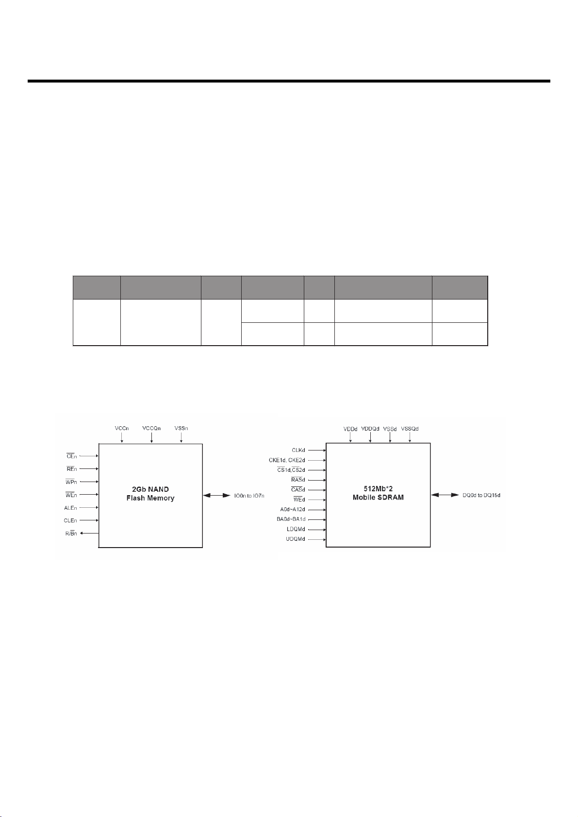
• 2Gb NAND flash memory +1G SDRAM
DD evicece P art Nam e M akerer Itemem Tim e S ize Speeeed
Program sp eed 2 00µs1Page=(2K + 64)Bytes 10 .32M Byte/s
Erase spee d 1 .5m s 1Block=(128K+4K)Bytes 88M B yte/s
NAND flash KAL0 0900BM -DJ55 Samsung
Figure 3-1-1 KF755d Block Diagram
Figure 3- 1- 2. External Memory Configuration of KF755d
• Data Communication
- IrDA ® (SIR)
- UARTs (ACB, EDB (RS232))
- Slave USB
• Package
- 12 by 12 mm 344 balls, 0.5mm pitch
FPBGA Production Package
Page 24
LGE Internal Use Only
Copyright © 2008 LG Electronics. Inc. All right reserved.
Only for training and service purposes
3. TECHNICAL BRIEF
- 25 -
3.1.3 Hardware Architecture
A. Block Diagram
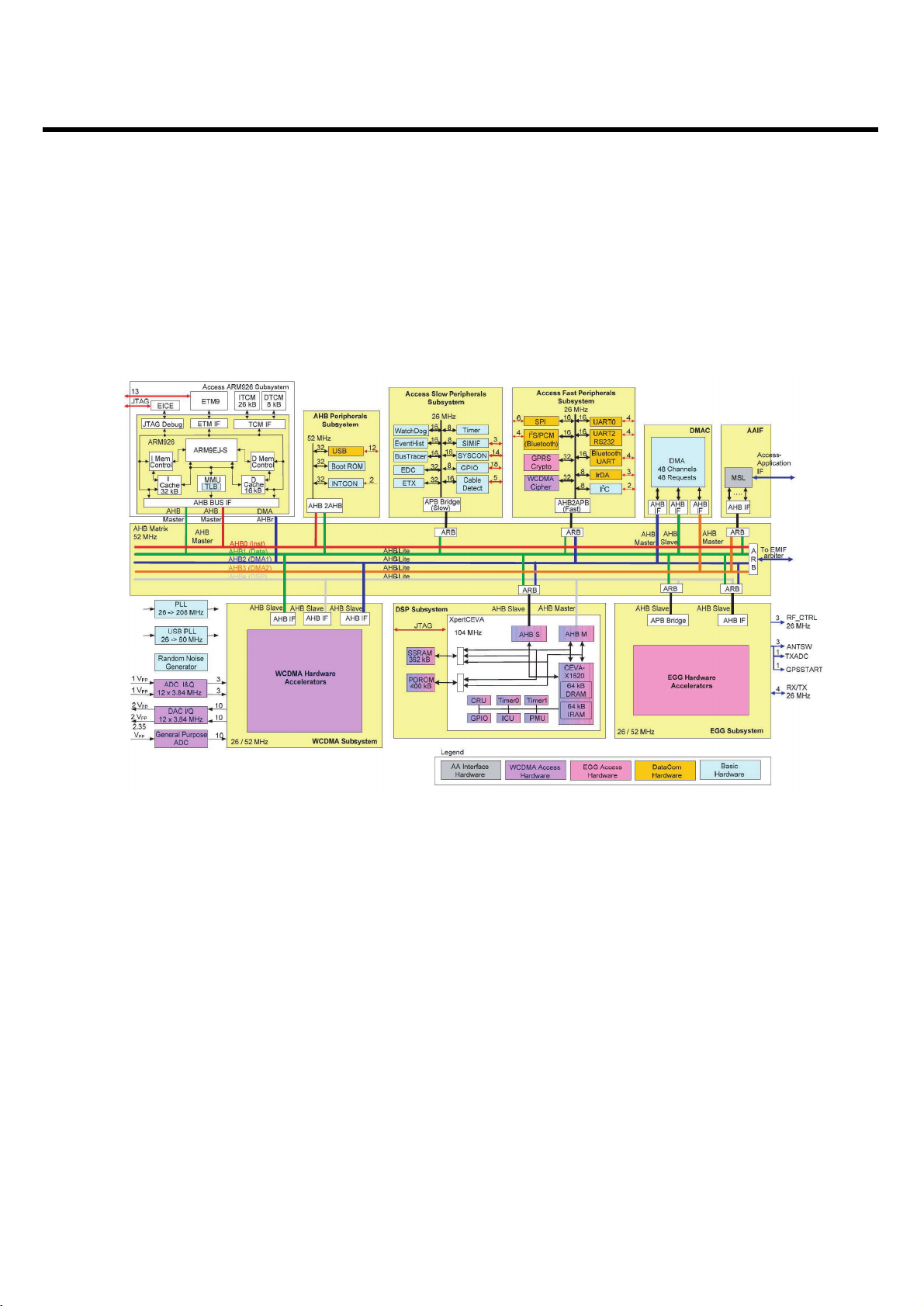
Figure 3-1-3. Access system of Ericsson DB3150
Page 25
LGE Internal Use Only
Copyright © 2008 LG Electronics. Inc. All right reserved.
Only for training and service purposes
3. TECHNICAL BRIEF
- 26 -
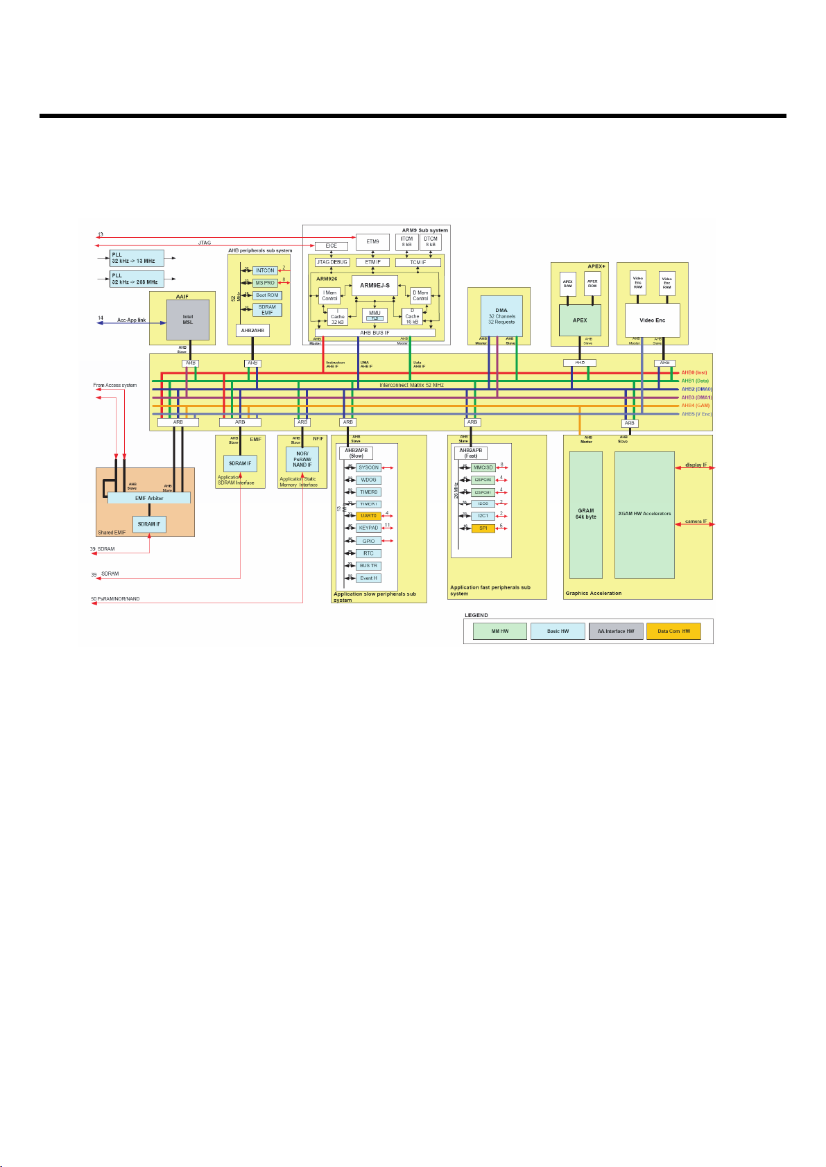
Figure 3-1-4. Application system of Ericsson DB3150
Page 26

LGE Internal Use Only
Copyright © 2008 LG Electronics. Inc. All right reserved.
Only for training and service purposes
3. TECHNICAL BRIEF
- 27 -
B. CPU Subsystem
• Access CPU subsystem
The digital baseband controller includes an access CPU subsystem, which includes the submodules
described below.
- 32 KiB I-cache
- 16 KiB D-cache
- Page table
- Memory Management Unit (MMU)
- JTAG
- ETM9
- 26 KiB I-TCM
- 8 KiB D-TCM
• Application CPU subsystem
The digital baseband controller includes an Application CPU subsystem, which includes the
submodules described below.
- 32 KiB I-cache
- 16 KiB D-cache
- Page table
- MMU
- JTAG
- ETM9
- 8 KiB I-TCM
- 8 KiB D-TCM
C. Peripheral Hardware Subsystem
The digital baseband controller includes hardware that supports mobile terminal peripherals such as a
MMC, SD, UART, I2C, USB, keypad, and infrared. Collectively, this hardware comprises the
Peripheral subsystem.
The functional blocks of the Peripheral subsystem connect to the peripheral bus through four separate
bridges, which provide a simple interface to support different timing and memory access
arrangements.
Page 27

LGE Internal Use Only
Copyright © 2008 LG Electronics. Inc. All right reserved.
Only for training and service purposes
D. DSP Hardware Subsystem
The Digital Signal Processor Subsystem (DSPSUB) includes a DSP megacell, which contains the DSP
CPU together with a tightly coupled memory. The DSP is the Ceva-X 1620 core with a 64 kB
instruction RAM and a 64 kB data RAM. It also contains debug logic and interfaces. In addition to the
megacell, the DSPSUB includes external memories, peripheral units, and interfaces. The DSP
megacell is clocked at 208 MHz.
The DSPSUB includes an AHB master and an AHB slave interface. The AHB master provides a direct
access to the Internal Random Access Memory (IRAM) in the EGG core through the AHB. The AHB
slave interface allows the CPU and the DMA to access in the program and data RAM residing in the
DSPSUB.
E. XGAM Subsystem
The XGAM subsystem is a graphics acceleration module that provides hardware support in the
creation of visual imagery and the transfer of this data to a display. The XGAM also provides support
for connecting a Camera module. The visual data could be graphics, still images, or video.
The XGAM subsystem is handled and provided by Ericsson.
F. System Control Subsystem
The SYSCON resides at the top level of the circuit architecture and is responsible for clock generation
and clock and reset distribution within the digital baseband controller, as well as to external devices.
The block is a slave peripheral under control of the ARM processor. The programming of the SYSCON
controls the fundamental modes of operation within the digital baseband controller. Individual blocks
can also be reset and their clocks held inactive by accessing the appropriate control registers.
3. TECHNICAL BRIEF
- 28 -
Page 28

LGE Internal Use Only
Copyright © 2008 LG Electronics. Inc. All right reserved.
Only for training and service purposes
3. TECHNICAL BRIEF
- 29 -
3.1.4 RF Interface
A. Asta Interface
Asta controls GSM RF part using these signals through GSM RF chip-Gimli.
• RF_DATA_A
• RF_DATA_B
• RF_DATA_C
• RF_DATA_STRB
B. WCDMA Radio Link Interface
• RF_WCDMA_PA_0_EN
• RF_WCDMA_PA_1_EN
• RF_WCDMA_DCDC_EN
• RF_WCDMA_PWRDET_EN
Y4
RF_DATA_A
RF_DATA_B
AA2
Y3
RF_DATA_C
Y2
RF_DATA_STRB
QDATA_AMP_MSB
IDATA_FREQ_MSB
AMP_LSB_FREQ_LSB
DCLK_DATSTR
Figure 3-1- 5. Schematic of Asta RF Interface
Figure 3-1-6. Schematic of WCDMA RF Interface
RF_DATA_STRB
RF_WCDMA_PA_0_EN
RF_WCDMA_PA_1_EN
RF_WCDMA_DCDC_EN
RF_WCDMA_PWRDET_EN
RF_DATA_A
RF_DATA_B
RF_DATA_C
ADC_I_NEG
ADC_I_POS
ADC_Q_NEG
ADC_Q_POS
Y4
AA2
Y3
Y2
AB8
V7
AB5
AB6
Y10
W10
W9
Y9
QDATA_AMP_MSB
IDATA_FREQ_MSB
AMP_LSB_FREQ_LSB
DCLK_DATSTR
WTX_BAND_1_EN
TP300
WDCDC_EN
WPOW_DET_EN
WRX_I_N
WRX_I_P
WRX_Q_N
WRX_Q_P
DAC_I_NEG
DAC_I_POS
Y8
W8
W7
WTX_I_N
WTX_I_P
Page 29
LGE Internal Use Only
Copyright © 2008 LG Electronics. Inc. All right reserved.
Only for training and service purposes
3.1.5 SIM Interface
SIM interface scheme is shown in Figure3-1-6.
SIMDAT0, SIMCLK0, SIMRST0 ports are used to communicate DBB(Asta) with ABB(Veronica) and
filter.
3.1.6 UART Interface
UART signals are connected to Asta GPIO through IO connector
3. TECHNICAL BRIEF
- 30 -
SIM (Interface between DBB and ABB)
SIMDAT0 SIM card bidirectional data line
SIMCLK0 SIM card reference clock
SIMRST0 SIM card async/sync reset
Resource Name Note
UART0
ACC_GPIO_2 ACC_UART_RX ACC Receive Data
ACC_GPIO_3 ACC_UART_TX ACC Transmit Data
UART1
APP_GPIO_0 APP_UART_RX APP Receive Data
APP_GPIO_1 APP_UART_TX APP Transmit Data
Table 3-1-2. SIM Interface
Table 3-1-3. UART Interface
Figure 3-1-7. SIM Interface
Asta
SIMDAT0
SIMCLK0
SIMRST0
VDD
E
10K
SDAT SIMDAT
SCLK SIMCLK
SRST
SIMVCC
Veronica
SIMRST
10K
VDD
DAT
CLK CARD
RST
Page 30

LGE Internal Use Only
Copyright © 2008 LG Electronics. Inc. All right reserved.
Only for training and service purposes
3.1.7 GPIO (General Purpose Input/Output) map
In total 39 allowable resources. This model is using 39 resources.
GPIO Map, describing application, I/O state, and enable level are shown in below table.
3. TECHNICAL BRIEF
- 31 -
Table 3-1-4. Asta ACC GPIO Map Table
DB3150's GPIO GPIO Mapping Init Status
ACC_GPIO_0 ACC_GP00_USB_STP Output low
ACC_GPIO_1 ACC_GP01_USB_DIR input
ACC_GPIO_2 ACC_GP02_UART0_RX input
ACC_GPIO_3 ACC_GP03_UART0_TX Output
ACC_GPIO_4 ACC_GP04_USB_CLK input
ACC_GPIO_5 ACC_GP05_USB_NXT input
ACC_GPIO_6 ACC_GP06_USB_DAT4 input / Output
ACC_GPIO_7 ACC_GP07_USB_DAT5 input / Output
ACC_GPIO_8 ACC_GP10_USB_DAT6 input / Output
ACC_GPIO_9 ACC_GP11_USB_DAT7 input / Output
ACC_GPIO_10 ACC_GP12_TOUCH_LDO_EN Output low
ACC_GPIO_11 ACC_GP13_SPK_AMP_EN Output low
ACC_GPIO_12 ACC_GP14_BT_SPI_INT Input
ACC_GPIO_13 ACC_GP15_FLIPSENSE Input
ACC_GPIO_14 ACC_GP16_FM_GPIO2 Input
ACC_GPIO_15 ACC_GP17_PHFSENSE Input
ACC_GPIO_16 ACC_GP20_USB_CS_PD input / Output
ACC_GPIO_17 ACC_GP21_VC_IO_OFF Output low
ACC_GPIO_18 ACC_GP22_USB_DAT3 input / Output
ACC_GPIO_19 ACC_GP23_BT_SPI_CS0n Output
ACC_GPIO_20 ACC_GP24_BT_SPI_DAT0 Output low
ACC_GPIO_21 ACC_GP25_BT_SPI_DAT1 Input
ACC_GPIO_22 ACC_GP26_BT_SPI_CLK Output low
ACC_GPIO_23 ACC_GP27_AMP_SW_EN Output low
Page 31

LGE Internal Use Only
Copyright © 2008 LG Electronics. Inc. All right reserved.
Only for training and service purposes
3. TECHNICAL BRIEF
- 32 -
Table 3-1-5. Asta APP GPIO Map Table
Table 3-1-5. MMIC APP GPIO Map Table
DB3150's GPIO GPIO Mapping Init Status
APP_GPIO_0 APP_GP00_UART_RX Input
APP_GPIO_1 APP_GP01_UART_TX Output
APP_GPIO_2 APP_GP02_MMP_INT_n Input
APP_GPIO_3 APP_GP03_MMP_PWR_EN Output low
APP_GPIO_4 APP_GP04_TOUCH_SCREEN_INT Input
APP_GPIO_5 APP_GP05_TOUCH_SCREEN_SCL Output
APP_GPIO_6 MICROSD_DAT3 Input
APP_GPIO_7 APP_GP07_3AXIS_INT Input
APP_GPIO_8 APP_GP10_MMP_RESET_N Output low
APP_GPIO_9 APP_GP11_REMOTE_INT Input
APP_GPIO_10 APP_GP12_LCD_ID Input
APP_GPIO_11 APP_GP13_MC_CLKRET Input
APP_GPIO_12 SUB_PM_RESETB Output low
APP_GPIO_13 MOTOR_EN Output low
APP_GPIO_14 APP_GP16_TOUCH_SCREEN_SDA input / Output
DB3150's GPIO GPIO Mapping Init Status
GPIO_0 CI_VSYNC_WITHOUT_FF Output low
GPIO_1 APP_GP05_TOUCH_RESET Output low
GPIO_2 CI_VSYNC Output low
GPIO_3
GPIO_4 MMP_CAM_RESET_N Output low
GPIO_5 MMP_CAM_PWR_EN Output low
GPIO_6 MMP_CAM_PWDN Output low
GPIO_7 FLASH_LED_EN Output low
GPIO_8 FLASH_LED_TORCH Output low
GPIO_9 FLASH_LED_INH Output low
Page 32

LGE Internal Use Only
Copyright © 2008 LG Electronics. Inc. All right reserved.
Only for training and service purposes
3. TECHNICAL BRIEF
- 33 -
3.1.8 USB
The USB block supports the implementation of a °∞High-speed" device fully compliant to USB 2.0
standard. It provides an interface between the CPU (embedded local host) and the USB wire, and
handles USB transactions with minimal CPU intervention.
The USB specification allows up to 15 pairs of endpoints. Data for each endpoint is buffered in RAM
within the USB block and is read/written from the endpoint FIFO using DMA transfers or FIFO register
access. High-speed (high throughput) endpoints can use DMA while slower endpoints can use FIFO
register access.
The USB block can request up to six DMA channels, three for IN endpoints and three for OUT
endpoints.
USB Function Note
USB_STP ULPI stop signal
USB_DIR ULPI direction signal
USB_CLK USB clock
USB_NXT ULPI next signal
USB_DAT0 USB data0
USB_DAT1 USB data1
USB_DAT2 USB data2
USB_DAT3 USB data3
USB_DAT4 USB data4
USB_DAT5 USB data5
USB_DAT6 USB data6
USB_DAT7 USB data7
USB_CS_PD USB chip select
VBUS Power supply for Asta USB block
Table 3-1-6. USB Signal Interface of Asta
Page 33

- 34 -
3. TECHNICAL BRIEF
LGE Internal Use Only
Copyright © 2008 LG Electronics. Inc. All right reserved.
Only for training and service purposes
A
A
A
A
Figure 3-1-8. Schematic of Asta USB block
A
Figure 3-1-9. Schematic of USB Transceiver
PTS_BSU_00PG_CCA
RID_BSU_10PG_CCA
C
C
0PG_
A
X
_0TRAU_2
R
XT_0TRAU_30PG_CCA
KLC_BSU_40PG_CCA
TXN_BSU_50PG_CCA
4TAD_BSU_60PG_CC
5TAD_BSU_70PG_CC
C
U_
_
C
D
BS
01PG
6TA
_
7TAD_BSU_11PG_CC
USB_DAT1
USB_DAT0
USB_DAT2
9J
9K
2P
A
9
N
A
9M
4N
3P
A
4P
A
R
4
3R
2
R
L4
USB_DAT_VP
L3
USB_SE0_VM
M4
USB_OE
CCA
0_OIPG_CCA
1_OIPG
_CCA
2_OIPG_CC
3_OIPG_CC
4_OIPG_
5_OIPG_CCA
6_OIPG_CC
7_OIPG_CC
8_OIPG_CCA
9_OIPG_CCA
TABV
8V
1_EDDV
106C
00
6C
u7
.4
u1.0
60
30
V01
F1
F2
F3
C
3
DP_SC_BSU_02PG_CC
R603 51K
A
CA
KLC_BSU_40PG_CCA
0TAD_BSU
1TAD_BSU
2TAD_BS
U
3TAD_BSU_22PG_CCA
4TAD_BSU_60PG_CCA
5
TAD_BSU_70PG_CCA
6TAD_BSU_01PG_CCA
7TAD_BSU_11PG_CC
N_BSU_50PG_CCA
TX
PTS_BSU_00PG_CCA
ID_BSU_10PG_C
R
0.1uC603
4.7u
C602
C
4
A
C
1B
1A
TAD
2A
3A
D
5A
6A
6B
6C
5
D
6
D
P
TS
5E
RID
1E
6E
0
306
NC1
NC2
LES_PIHC
VCC
KCOL
0ATAD
1A
2ATAD
106U
3ATA
4ATAD
5ATAD
6ATAD
7ATAD
0GFC
8V1FER
GND1
GND2
GND3
E4
D2
4
TSET
5B
1OI_CCV
2B
2OI_CCV
2C
RR
FE
1C
MD
1D
PD
2E
TEA8051PSI
TLUAF
3D
DI
3B
2
GFC
4B
1
GFC
4
D
N_WSPTXN
F
4
SUBV
3E
3
V3GER
5
F
1LATX
6F
TX
2LA
C5
0.1uC604
60
0.1u
1%
30
R606 12K
C605
6R
2.2uC607
4.7uC606
3060
U
MD_BS
PD
U
_BS
K150
U_SUBV
XRT_BS
1LATX_BSU
deepS hgiH rof reviecsnarT BSU
Page 34

- 35 -
3. TECHNICAL BRIEF
LGE Internal Use Only
Copyright © 2008 LG Electronics. Inc. All right reserved.
Only for training and service purposes
3.1.9 Slider ON/OFF Detection
There is a magnet to detect the slide module status, up or down.
If a magnet is close to the hall-effect switch U101, the voltage at Pin 4 of U101 goes to 0V.
Otherwise 1.8V.
This SLIDE_DET signal is delivered to Asta ACC_GP15_FLIPSENSE.
Figure 3-1-10. Slider On/Off Detector
LS
I
57V2_GDDV
1
DV
D
2
901C
u1.0
3
1DNG
N
C
TCETED ED
DV
5MB21006KT101U
6
DDV_OI
5
2DNG
4
UO
T
8V1_ED
NESPILF_51PG_CCA
ES
211
C
u1.0
Page 35

LGE Internal Use Only
Copyright © 2008 LG Electronics. Inc. All right reserved.
Only for training and service purposes
3. TECHNICAL BRIEF
- 36 -
3.1.10 Bluetooth Interface
KF755d supports Bluetooth operation using STLC2593C Bluetooth module.
A. General Description
The Bluetooth interface utilizes the SPI interface for control signals going to and from the Bluetooth
module. The SPI is also used for data transmissions.
It uses the PCM interface for transmitting audio to and from the Bluetooth module.
The Bluetooth module uses both the 26 MHz master clock signal and the 32,768 kHz low-frequency
clock signal for internal timing within the Bluetooth module. The intention is to use the low-frequency
clock as a low-power timing provider and to use the 26 MHz as a high precision timing reference used
mainly by the Bluetooth radio during operation.
The clock request mechanism is used to minimize current consumption for the total system.
The intention is to use the CLKREQ signal to ask for the master clock when needed, for example,
when the Bluetooth radio is operating.
B. SPI Interface
The physical SPI interface is made up of 5 signals : clock, chip select, data in, data out and interrupt.
When the SPI mode is selected , these signals are available through the BT_UART and
BT_HOST_WAKEUP pins.
The SPI interface is Master at the Host side, and Slave at the BT Controller side.
It is designed to work with the H4 protocol. It does not support HCI synchronous data packet transfer.
Data are transferred on the SPI interface in byte format, LSB first.
The SPI interface can operate only in half duplex mode.
C. PCM Interface
The PCM interface is used to send audio to and from the Bluetooth module. The interface is a
synchronous interface using a PCM clock and a PCM sync signal for synchronization. Two data
signals are used for data, one in each direction.
The PCM clock signal operates at frequencies as high as 1 MHz. The word length of the audio data
can be 8 or 16 bits. Furthermore, the PCM interface has a function known as MP-PCM, which is an
addressing scheme, used to have more than two devices talking on the bus.
To add this function, the data pins have to be bi-directional. Additionally, the position of the audio data
relative to the frame sync pulse must be selectable. During the periods within a frame that a device is
not transmitting audio data, it must put both PCM data signals in a high-impedance state to allow other
devices access.
Page 36

D. Master Clock and Clock Request Interface
The master clock (MCLK) is a 26 MHz signal used as the high precision clock signal for the Bluetooth
module. The signal can be switched on and off by the platform. The master clock request (CLKREQ) is
used by the Bluetooth module to ask for the master clock.
If the Bluetooth module asserts the signal high, it gets the master clock. The other alternative for the
Bluetooth module is to set the clock request output to high impedance state, indicating that it does not
need the master clock. The Bluetooth module receives the master clock, if other parts of the chipset
request it.
E. Low Frequency Clock Interface
The low-frequency clock signal (RTCCLK) is used by the Bluetooth module as a low-power clock. The
clock is used in different Bluetooth modes, like sniff and park, to have a correct timing on the Bluetooth
air interface without having the master clock running.
The low-frequency clock is always present, in some applications even when the chipset is powered
down.
F. STLC2593C
■ WFBGA 5.0 x 7.5 x 0.8 mm lead-free/RoHs compliant 100 pins
■ External component: B-BPF (Bluetooth)
■ PCB footprint < 45mm2
■ Based on Ericsson Technology Licensing Baseband Core (EBC)
■ Bluetooth¢‚ specification compliance: V2.0 + EDR.
- Point-to-point, point-to-multi-point (up to 7 slaves) and scatternet capability
- Support ACL and SCO links
- Extended SCO (eSCO) links
- Faster Connection
■ HW support for packet types
- ACL: DM1, DM3, DM5, DH1, DH3, DH5, 2-DH1, 2-DH3, 2-DH5, 3-DH1, 3-DH3, 3-DH5
- SCO: HV1, HV3 and DV
- eSCO: EV3, EV4, EV5, 2-EV3, 2-EV5, 3-EV3, 3-EV5
- Adaptive Frequency Hopping (AFH)
■ Transmit Power
- Power Class 2 and Power Class 1.5 (above 4dBm)
- Programmable output power
- Power Class 1 compatible
LGE Internal Use Only
Copyright © 2008 LG Electronics. Inc. All right reserved.
Only for training and service purposes
3. TECHNICAL BRIEF
- 37 -
Page 37

LGE Internal Use Only
Copyright © 2008 LG Electronics. Inc. All right reserved.
Only for training and service purposes
3. TECHNICAL BRIEF
- 38 -
■ HCI
- HCI H4 Transport Layer
- HCI proprietary commands (e.g. peripherals control)
- Single HCI command for patch/upgrade download
■ Supports Pitch-Period Error Concealment (PPEC)
■ Efficient and flexible support for WLAN coexistence in collocated scenario
■ Low power consumption
- Ultra low power architecture with 3 different low-power levels
- Deep Sleep modes, including Host power saving feature
- Dual Wake-up mechanism: initiated by the Host or by the Bluetooth device
■ Communication interfaces
- Fast UART up to 4Mbit/s
- SPI interface
- PCM interface
- Up to 10 additional flexibly programmable GPIOs
- External interrupts possible through the GPIOs
- Fast master I2C interface
■ Clock support
- System clock input (digital or sine wave) at9.6, 10, 13, 16, 16.8, 19.2, 26, 33.6 or 38.4MHz
- Low Power clock input at 32.768 kHz
■ ARM7TDMI CPU
■ Memory organization
- On chip RAM, including provision for patches
- On chip ROM, preloaded with SW up to HCI
■ Ciphering support up to 128 bits key
■ Single power supply with internal regulators for core voltage generation
■ Supports 1.65 to 2.85 Volts IO systems
■ Auto calibration (VCO, Filters)
Page 38

LGE Internal Use Only
Copyright © 2008 LG Electronics. Inc. All right reserved.
Only for training and service purposes
3. TECHNICAL BRIEF
- 39 -
G. KF755d Bluetooth Schematic
• Clock
- Clock request
→ Connected to CLKREQ of Asta and Veronica, input to Gimly
- Fast clock : 26MHz
→ Supplied MCLK from Gimly
→ Frequency deviation : ± 20ppm
- Low power clock : 32.768kHz
→ Supplied RTCCLK from Veronica
• Power
- Supplied 2.75V, 1.8V from internal regulators of Veronica
• Reset
- RESOUT2_n signal of Asta controls STLC2593C reset.
• SPI
- Connected to SPI of Asta
- HCI interface between Asta and STLC2593C
• PCM
- Audio signal interface between Asta/Veronica and STLC2593C
• ANT
- 2.4GHz, 50 ohm matching
A
Figure 3-1-11. Schematic of STLC2593C
108PT
0
1
U
8
308
R
KLC_TB
0
008C
IND
8V1_EDDV
ABV
T
8V1_EDDV
R808
100K
C
2OIPG_MF_61PG_C
8
DDV
V1_E
R
n_2TUOSE
108C
IND
EGNAHC TON OD
KLCCTR
1TAD_IPS_TB
A
_52PG_CC
KLC_IPS_TB_62PG_CCA
C
A
NYS_MCP_CC
KLC_MCP_CCA
DLD_MCP_CCA
DLU_MCP_CCA
NI_IPS_TB_41PG_CCA
T
n_QERKLC_TB
57V2_KDDV
R807 0
C809 0.1u
PT
418
UOSER
n_1T
L
A
CS_C2I_PP
KLCCTR
7K
6
F
B
K
9
9L
9H
K
6
B
N
4
MCP_T
B
4
M
5K
A_MCP_TB
5M
MCP_T
B_
B
3
M
118PT
908PT
018PT
218PT
3K
K
4
B
3J
3
L
TB
9G
B
7E
9
F
8E
7
L
7M
B
6
N
8J
2B
RVSR_T
B
C
3
B
8
M
RVS
R_TB
1C
C
2
2M
B
4J
C_GE
R_TB
N
7
DVH_T
B
6E
B
0.1u
4
D
CN
1
7
F
2CN
C810
8F
3C
N
4
L
4CN
5
L
CN
5
6L
6CN
4A
AV_MF
3
B
DV_MF
7A
1OIPG_MF
6A
2OIPG_MF
5
A
MF
3OIPG_
8
B
PIMF_MF
9C
BTSR_MF
7
D
K
LCR_MF
D
9
NES_MF
B
9E
KLCS_MF
10p
22nC815
C814 22n
C816
2
T
95
3
C
S
L
7J
1_T
NTESER_TB
KLC_PL_TB
P
UEKAW_TB
R_TRAU_TB
YS_
9_OIPG_TB
1
1_OIPG_TB
01_OIPG_T
61_OIPG_TB
8_OIPG_
0_OIPG_T
W_TSOH_TB
_GIFNOC_TB
_GIFNOC_T
_GIFNOC_TB
D_
N_RVSR_TB
FR_RVSR_T
DLC_DDV_T
UO_QER_KLC_TB
_KLC_FER_T
NI
DX
STC_TRAU_T
CN
KLC_MCP_TB
1_NI_QER_KLC_TB
NI_QER_KLC_TB
2_
PUEKA
1
2
3
1LC_
2LC_RVSR_T
MSD_RVSR_TB
LRT
7G
T_TRAU_TB
DX
6
J
STR_TRAU_
TB
1K
PFR_TB
1J
NFR_T
B
6
M
A_OIV_TB
9J
B_O
IV_TB
3
N
C_OIV_TB
5N
D_OIV_TB
8G
E_OIV_TB
H
6
GIDSSV_TB
1
7H
DSSV_TB
2GI
H
8
3GIDSSV_TB
8K
DSSV_T
4GI
B
8L
5GIDSSV_TB
1D
B
1ANASSV_T
2D
2ANASSV_TB
3E
ASSV_
3AN
TB
1F
ANASSV_TB
4
F
2
5AN
TB
ASSV_
3F
6ANASSV_TB
4F
B
7ANASSV_T
1G
B
8ANASSV_T
3G
9AN
TB
ASSV_
G
4
01ANASSV_TB
3H
2_TUO_QER_KLC_TB
ASSV_T
11AN
B
4
H
1ANASSV_TB
2
1H
RSSV_TB
1F
L
1
FRSSV_TB
2
2
J
RSSV_
3F
TB
K
2
FRSSV_TB
4
2L
1AVH_TB
3
D
VH_T
2A
B
1E
3AVH_TB
2E
4AVH_TB
4E
5AVH_TB
2H
B
1TSET_T
2G
B
2TSET_T
6G
GRP_FA_TB
5C
T
UOR_MF
B
5
UOL_M
T
F
D
6
OIV_MF
8D
OI
DS_MF
A
3
1D
MF
NG_
B
4
2
DNG_MF
B
6
3DNG_MF
7B
4
DNG_MF
C
4
5D
MF
NG_
6C
6
DNG_MF
C
7
7
DNG_MF
5D
DNG_MF
8
C
8
F
DNGFR_M
F+( htooteulB
DV
ANA_TB_SSV
FR_TB_SSV
808C
0
u1.
ANA_TB_SSV
)oidaR M
0TAD_IPS_TB_42PG_CCA
n0SC_IPS_TB_32PG_CCA
5
B
4
B
8V
1_ED
08BF
0
06
408
C
u1.0
KDDV
_EDDV
DS_C2I_PPA
A
0
1C3407-TB054212AED008LF
1
U
1P
PB_
2
D_PB2P
C
G2
3G16
V
FR_TB_SSV
7V2_
5
8V1
318C
u1.
C817
120p
C803
8TUO
10
1nH
08CHn9.3
2
008L
n3.
H
3
FR_TB_SS
u1118C
u1
21
8C
O
U
O
308TU
208T
p
2.1
108L
FR_TB_SSV
PR_M
F
PL_MF
TNA_MF
Page 39

LGE Internal Use Only
Copyright © 2008 LG Electronics. Inc. All right reserved.
Only for training and service purposes
3. TECHNICAL BRIEF
- 40 -
3.1.11 MicroSD Interface card
KF755d supports the MicroSD card interface as external memory card.
MicroSD card has 4-data line, so KF755d uses 4-data line.
All control and data line is connected to Asta.
Cause of the difference between Asta and MicroSD card, a level shifter should be added.
• Card detection
- When there are no card in MicroSD card socket, REAL_MICROSD_DAT3 pin is high cause of an
internal pull-up.
- If Card is inserted in socket, The pull up can be disconnected by using SET_CLR_DETECT
command.
- VDDG_2V75 always supply power.
A
Figure 3-1-12. MicroSD card and Schematic of MicroSD card Interface
MicroSD card Interface
MICROSD_CMD Command/Response
MICROSD_CLK Clock
MICROSD_DAT Data line
VDDG_2V75 Supply voltage from Veronica internal LDO
Table 3-1-7. MicroSD card Interface
8V1_EDDV
246
8
RA1
0TAD_DSORCIM
CIM
M
M
RID_TAD_DSOR
TAD_DSORCI
1
2TAD_DSORCIM
TAD_DSORCI
3
RID_DMC_DSORCIM
D
MC_DSORCIM
KLC_DSORCIM
TERKLC_CM_3
1PG_PP
135
100K
7
R907
470K
5A
CV
AC
C
5
TAD
RID_0
2B
A0TAD
C
1
RID_321TAD
D
A1TA
B
4
A
4
D
A3TA
B
5
C
RID_DM
1B
ADMC
3A
AKLC
A
1
F_KL
C
3B
1DNG
3C
NG
109C
u1.0
2D
RYXZE604ACVA47NS009U
D
5
CCV
B
2D
B0TA
D
1D2A
D
B1TA
C
4
B2TADA2TAD
4D
B3TAD
C
2
BDMC
3D
BKLC
57V2_GDDV
246
8
RA2
309C
0
u1.
100K
3
5
7
1
R916 100K
TAD_DSORCIM_LAER
0
1TAD_DSORCIM_LAER
2TAD_DSORCIM_LAER
RCIM_LAER
3TAD_DSO
DMC_DSORCIM_LAER
KLC_DSORCIM_LAER
DNI
R941
Page 40

LGE Internal Use Only
Copyright © 2008 LG Electronics. Inc. All right reserved.
Only for training and service purposes
3. TECHNICAL BRIEF
- 41 -
3.1.1 Power On Sequence
User presses END key and then ONSWAn signal is changed to Low.
Veronica initiates the internal oscillator and powers on the regulators.
Veronica generates a power for Asta.
Veronica releases the power reset signal(PWRRSTn) and generates an interrupt(IRQ0n) to Asta.
Figure 3-1-13. Power On Sequence
Press
END key
ONSWA
Veronica
Power for Asta
PWRRST
n
ONSWA
IRQ
PWRRSTn
IRQ0n
Asta
RESPOW_N
IR
Q0_N
Page 41

LGE Internal Use Only
Copyright © 2008 LG Electronics. Inc. All right reserved.
Only for training and service purposes
3. TECHNICAL BRIEF
- 42 -
3.1.13 KeyPad, Touch button and Touch screen
There are 21 buttons and 5 side keys and touch button in Figure 2-1-13/14. Shows the Keypad circuit.
‘END’ Key is connected ONSWAn for Veronica.
When Touch button and Touch screen is touched, Interrupt is given to Asta than, she read the status
register what button is touched by I2C. I2C is realize by Asta GPIO.
Figure 3-1-14. KEY CIRCUIT
Table 3-1-8. Key Matrix Mapping Table
KEYIN0 KEYIN1 KEYIN2 KEYIN3 KEYIN4 KEYIN5
KEYOUT0 VOLUME1 VOLUME2
KEYOUT1 1 2 3 MULTI SEND OK
KEYOUT2 4 5 6 CAMAF CLR
KEYOUT3 7 8 9 CAMSHOT
KEYOUT4 * 0 # HOME
8V1_EDD
V
246
8
10
1AR
101
K
01
135
7
YEK
1TUO
K
2TUOYE
3TUOYEK
0NIYEK
4TUOYEK
1NIYEK
2NIYEK
3
NIYEK
DNE
S
1TUOYEK
2TUOYEK
4NIY
EK
5NIYEK
8
V1_EDDV
RLC
009RK
01
109R
K01
1
015
4
45
701
7
4TO
H
K
O
009D
03-S125BR
YEK_REBMUN
1
2
1
0
8019
8
011
0
3
0120
3
601
6
1
0
9
201TOH101TOH
H
5TO
n_AWSNO
n_AWSNO
009AV
R
I
F053X4150SVC
_
K WS
NO
YE
2TUOYEK
3TUOYEK
3NIYE
K
1TUOYEK
4TUOYEK
3NIYEK
DNE
4
3
0TUOYE
K
0NIYEK
I
1
YEK
N
1
011WS
1
2
ITLU
M
EMOH
307NC
1
2
3
4
Page 42

LGE Internal Use Only
Copyright © 2008 LG Electronics. Inc. All right reserved.
Only for training and service purposes
3. TECHNICAL BRIEF
- 43 -
A
Figure 3-1-15. Touch button and Touch screen connector
I2C interface
V1.3_HCUOT
109NC
8171
1
2
3
4
5
6
41
31
21
11
0
1
9
87
6151
R905
DNI
R906
4.7K
R907
4.7K
TNI_NEERCS_HCUOT
LCS_NEERCS_HCUOT
DS_NEERCS_HCUOT
Page 43

LGE Internal Use Only
Copyright © 2008 LG Electronics. Inc. All right reserved.
Only for training and service purposes
3. TECHNICAL BRIEF
- 44 -
3.1.14 Multi EL lighting
There are 13 EL lighting channel. Each lighting channel is operated independently. EL
controller(U901) control AC generator and EL driver(U900). AC generator generate 190V AC signal.
And this 190V AC signal is switched by EL driver. Through EL driver, AC signal of the each lighting
channel is switched independently. Finally, switched AC signal illuminate EL sheet.
Figure 3-1-16. Multi EL lighting
EL controller AC generator EL driver EL lighing channel
output (connected with
EL sheet)
VREG_6.1V
C902
2.2u
TOUCH_3.1V
0.1u
C904
TP902
28
32
33
GND
VSS1
1
P0_1
2
P2_7
3
P2_5
4
P2_3
5
P2_1
6
P3_3
7
P3_1
8
P1_7
P1_3
P1_5
9
10
30
29
31
P0_5
P0_3
U901
CY8C21434
VSS2
P1_1
12
13
11
P0_7
P1_0
26
27
25
VDD
P0_4
P0_6
P0_2
24
P0_0
23
P2_6
22
P2_4
21
P2_2
20
P2_0
19
P3_2
18
P3_0
17
XREX
P1_2
P1_4
P1_6
14
15
16
0
R909
L900
100uH
D5
D1 D2 D3 D4
Q900
SIA450DJ
G
S1 S2
R912
100K
TOUCH_SCREEN_SCL
TOUCH_SCREEN_SDA
I2C
D901
RF051VA2S
TOUCH_RST
R910
C903
470pF
R913
TP905
TP906
TP907
TOUCH_BUTTON_SCL
TOUCH_BUTTON_SDA
100K 10M
ISSP
C905
150p
TOUCH_3.1V
C907
0.1u
C906
0.1u
U900
SLUG
NC5
NC4
NC3
NC2
NC1
_POL
_LE
GND
DOUT
CLK
DIN
VDD
HV509
33
25
23
18
16
13
21
22
15
24
19
17
20
HVGND
HVOUT16
HVOUT15
HVOUT14
HVOUT13
HVOUT12
HVOUT11
HVOUT10
HVOUT9
HVOUT8
HVOUT7
HVOUT6
HVOUT5
HVOUT4
HVOUT3
HVOUT2
HVOUT1
VBIAS
VPP
28
BP
27
TP903
29
30
31
32
1
2
3
4
5
6
7
8
9
10
11
12
14
26
R91556K
HV_OUT_14
HV_OUT_13
HV_OUT_12
HV_OUT_11
HV_OUT_10
HV_OUT_9
HV_OUT_8
HV_OUT_7
HV_OUT_6
HV_OUT_5
HV_OUT_4
HV_OUT_3
HV_OUT_2
BP
Page 44

LGE Internal Use Only
Copyright © 2008 LG Electronics. Inc. All right reserved.
Only for training and service purposes
3. TECHNICAL BRIEF
- 45 -
3.2 GAM Hardware Subsystem
3.2.1 General Description
The Graphics Accelerator Module (GAM) subsystem provides hardware support in the creation of
visual imagery and the transfer of this data to the display. GAM also provides support for the camera
module. The visual data could be graphics, still images or video. The GAM subsystem consists of five
modules:
• GRAM : graphics memory (160 kB).
• GAMCON : GAM controller.
• GRAPHCON : graphics controller.
• PDI/SSI : programmable display interface for parallel/serial displays.
• CDI : camera data interface.
Figure 3-2-1. GAM Subsystem Functional Block Diagram
Page 45

LGE Internal Use Only
Copyright © 2008 LG Electronics. Inc. All right reserved.
Only for training and service purposes
3. TECHNICAL BRIEF
- 46 -
3.2.2 Block Description
A. GAM Controller(GAMCON)
The GAM Controller (GAMCON) is responsible for clock gating and distribution within the GAM
module. GAMCON receives the HCLK from SYSCON and distributes to GRAPHCON, GRAM, PDI and
CDI. GAMCON also distributes the GAM reset signal to GRAPHCON, GRAM, PDI and CDI.
The reset signals CIRES_N and PDIRES_N are distributed from GAMCON to the camera and display
module respectively, see Figure 2.28. The CIPCLK is used to clock the received data into the camera
data interface. The CIPCLK can be in the range of 100 kHz to 16 MHz.
B. Graphics RAM (GRAM) Block
GAM includes 160 kB of graphics memory (GRAM) in order to support display screen sizes of QCIF +
alfa display size and three frame buffers when decoding QCIF video.
The GRAM can be accessed in 8, 16 or 32-bit mode. Write access takes a single AHB clock cycle.
Non-sequential read and the first access of a sequential read access takes two AHB clock cycles.
Subsequent sequential read access take a single AHB clock cycle.
The GRAM contains both frame buffer and temporary data. There are three image areas with one
used for normal MMI graphics and the other two areas used for still images, video frames or camera
frames. The three image areas can be combined into one frame buffer.
GRAM is required to transfer a VGA (640 by 480 pixels) image from the camera data interface (CDI)
over DMA at 100 MBit/s, within a 50 ms timeframe. The GRAM is used as a buffer, but the average
transfer bandwidth required is approximately 3 Mword/s (32-bit word), that is 12 MByte/s.
C. Graphics Controller (GRAPHCON) Block
GRAPHCON is controlled by the application CPU and can perform operations on pixels and image
areas. Images can be moved and merged with other images and text.
The GRAPHCON block receives graphical objects from GRAM and performers the appropriate
graphical manipulation. The resulting data is transfers to the display interface (PDI).
GRAPHCON can receive images from the camera data interface (CDI) and send them to the PDI
automatically.
GRAPHCON performs conversion from YUV to RGB and can scale (zoom) still or video images.
D. Programmable Display Interface (PDI) Block
The programmable display interface (PDI) is designed to interface both parallel and serial display
modules. The display data is transferred from the 32 word FIFO on GAMCON to the display module
via the PDI block. The PDI block is built around a micro controller and executes 16-bit instruction
words to individually control the I/O ports. It has a 128 byte program memory, programmable by the
CPU, which can store up to 64 instructions.
Page 46

LGE Internal Use Only
Copyright © 2008 LG Electronics. Inc. All right reserved.
Only for training and service purposes
3. TECHNICAL BRIEF
- 47 -
The CPU transfers all set-up and control data to the display. Data is transferred to PDI as 32- bit
words, which in turn writes 8-bit data to the display. The programmable PDI block is configured at the
software build stage, to support either parallel interface such as PPI or serial interface such as SSI or
I2C.
E. Camera Data Interface (CDI) Block
The camera data interface (CDI) block is designed to support a range of still image camera modules.
An 8-bit parallel bus supports data transfer from the camera module to the CDI.
The pixel clock is an output clock from the camera module to the CDI and qualifies the data on the
parallel bus. One byte of data is captured on each rising edge of the pixel clock. CDI allows the pixel
clock to be in the range of 100 kHz to 16 MHz.
The horizontal synchronization line is an input from the camera module and defines one scanline of
image data. The horizontal synchronization line can be programmed to be active high or low. The
vertical synchronization line is an input from the camera module and defines one image frame (image
height) of data. The vertical synchronization line can be programmed to be active high or low.
The frame rate can be adjusted by skipping frames and various interrupts are used to inform the
application CPU regarding the progress of incoming images and potential errors. The normal data
format on the data bus is YUV 4:2:2 (raw binary image data) according to the CCIR-656 standard. A
function within the CDI can be programmed to reorder the YUV parameters as they pass through the
CDI. In addition, the CDI is able to detect the end of an image and perform some truncation as well as
overflow conditions. There is nothing preventing the use of other data types such as JPEG or RGB (as
long as the timing is followed), but only YUV data can be sent to the display.
Camera images can also be sent to a DMA channel to store the image in external memory.
The I2C interface and GPIO are part of the interface to the camera module, but they are not part of the
CDI block. The I2C is used to set-up and control the camera module.
The camera module I2C lines must go high impedance when the supply is removed from the camera.
The I2C commands needed to control the camera, as well as the functional behavior of the module,
are also different for each implementation.
The ON-signal (GPIO) is used to power-on the camera from Standby or Off mode (implementation
dependent). This signal must be held low when the mobile equipment is powered down and during the
mobile equipment reset period. The GPIO pin can also be an input or high impedance during mobile
equipment reset and start. In this case, it must have pull-down to ground.
The camera module reset signal is an output to the camera module.
Page 47

LGE Internal Use Only
Copyright © 2008 LG Electronics. Inc. All right reserved.
Only for training and service purposes
3. TECHNICAL BRIEF
- 48 -
3.2.3 Camera & Camera Interface
Figure 3-2-2. Camera Interface (DB3150 and Zoran)
Figure 3-2-3. 5M Camera Connector(34Pin - Main Board)
VGA Camera 5 Mega Camera
21P
KLCMV
0
1P
LCPV
K
CI_PCLK
CI_RES_N
F20
E20
E19
CI_PCLK
CI_RES_n
CI_HSYNC
CI_VSYNC
F19
F18
CI_VSYNC
CI_HSYNC
CI_D1
CI_D0
G21
CI_D0
CI_D1
CI_D2
F21
CI_D2
CI_D3
G20
CI_D3
CI_D4
H21
CI_D4
CI_D5
G19
CI_D5
CI_D6
G22
CI_D6
CI_D7
H22
CI_D7
21M
FERHV
21K
S
VV
8P
ADIV
8N
B
DIV
9P
C
DIV
M
01
DDIV
01N
DIV
E
9N
F
DIV
N
11
GDIV
11P
HDIV
N
21
IDIV
7N
JD
IV
L
8
KDI
V
31P
DIV
L
9
L
V
DI
M
31
N
DIV
N
11M
ODIV
9M
PDIV
C
T
AR
5
I
N
EMAC M
E
FRE
A
CAM_AVDD_2.8V
CAM_VDD_1.8V
KLCM_MAC_PMM
C_PM
M
M
M
M
MM
C_PM
M
M
M
M
_PM
KLCP_MA
C
NYSH_MAC_PM
CNYSV_MAC_PMM
]0[ATAD_MAC_PMM
]1[ATAD_MAC_PM
]2[ATAD_MAC_PMM
]3[ATAD_MAC_PMM
]4[ATAD_MAC_PMM
]5[ATAD_MAC_PM
[ATAD_MAC_PMM
]6
]7[ATAD_MAC_P
]8[A
TAD_MA
]9[ATAD_MAC_PM
ATAD_MAC_PM
]01[
]11[ATAD_MAC
V8.2_FA_DDV_MA
C
9
]8[ATAD_MAC_PMM
_MAC_PMM
]9[ATAD
]
MM
01[ATAD_MAC_P
]11[ATAD_MAC_PMM
]7[ATAD_MAC_PMM
[ATAD_MAC_PM
]6
M
C_P
]5[ATAD_MA
MM
[ATAD_MAC_PMM
]4
D_MAC_PMM
]3[ATA
C_PM
]2[ATAD_MA
M
]1[ATAD_MAC_PMM
C_P
]0[ATAD_MA
MM
NI
8
7
I
6
NI
8101EVCI
9
8
7
6
NI
9
NI
8
I
7
6
007LF
1R070E48101EVCI
RF00
1
1A_TUONI
1B_TUO
2
I
2A_TUON
2B_TUONI
3
ONI
3B_TUON
3A_TU
4
I
4B_TUO
4A_TUON
G110G2
5
107LF
RF001R070E4
1
1A_TUONI
1B_TUONI
2
I
2A_TUON
2B_TUONI
3
3A_TUONI
3B_TUONI
4
4A_TUONI
4B_TUO
G1
G2
5
10
207LF
RF001R070E48101EVCI
1
1A_TUONI
1B_TUO
2
I
2B_TUON
2A_TUON
3
3A_TUONI
3B_TUONI
4
4A_TUONI
4B_TUONI
G15G2
10
]8[ATAD_MAC_M5
]9[ATAD_MAC_M5
01[ATA
]
D_MAC_M5
11[ATAD_MAC_M
]
5
3320
7R
CM_MAC
M
KL
_PM
CP_MAC_
KL
PMM
_MAC_
]0[ATAD
M5
]1[ATAD_MAC_M5
]2[ATAD_MAC_M5
]7[ATAD_MAC_M5
]
_MAC_M5
6[ATAD
]5[ATAD_MAC_M5
]
TAD_MAC_M5
4[A
_MAC_M
]3[ATAD
5
M5
]2[ATAD_MAC_
]1[ATAD_MAC_M5
]0[ATAD_MAC_M5
]3[ATAD_MAC_M5
]4[ATAD_MAC_M5
]5[ATAD_MAC_M5
_M5
]6[ATAD_MAC
]7[ATAD_MAC_M5
]8[ATAD_MAC_M5
M5
]9[ATAD_MAC_
]01[ATAD_MAC_M5
1[A
]1
TAD_MAC_M5
01
307R
VA701
607
507
C
C
IND
IND
VA702ICVL0518100Y500FR
ICVL0518100Y500FR
107C
1.0
u
60
30
107NC
1
3
4
3
2
3
23
3
4
3
1
3
5
0
2
9
6
2
8
7
2
7
8
2
6
9
2
01
5
2
4
11
32
21
2
2
31
2
41
1
51
02
1
61
9
8
171
207C
u1
0
u1.
3060
01407
R
01507R
060
3
M
3060
607R
01
M
01707R
3060
M
_PM
060
3
M
30
FB700
4
07C
u1.0
306
0
VA700ICVL0518100Y500FR
C708
707C
0
u1.
3060
p01
C711
C710
C709
060
3060
p013
60
3060
01
p01
p
007C
307C
01
u
N_TESER_MAC_PMM
A
MM
DS_C2I_P
LCS_C2I_PM
NYSV_MAC_PM
C
NYSH_MAC
C
NDWP_MAC_PM
A
hgiH evitc
Page 48

LGE Internal Use Only
Copyright © 2008 LG Electronics. Inc. All right reserved.
Only for training and service purposes
3. TECHNICAL BRIEF
- 49 -
A
A
Figure 3-2-5. VGA LCD FPCB Connector
V8.2_DDV_AGV
V8.
1_DDV_AGV
201
C
0
K
X
A
FFO_OI_CV_12PG_CC
CSYS
0KL
KLCP_IC
0D_IC
D
1
IC
_
C
2D_I
3D_IC
IC
4D_
5D_I
C
1
2
3
4
5
6
7
8
9
3G
G
4
7
027
1
401NC
2G1G
02
1
9
1
8
1
7
61
51
1
4
1
3
21
1101
4G
u1.
1059100YBNE
301C
u1.
0
n_SER_IC
LCS_C2I_PPA
PA
DS_C2I_P
CNYSH_IC
CNYSV_IC
7D_IC
6
C
D_I
6001C
u1.0
Page 49

The 5M Camera modules are connected to 34-pin main board and VGA Camera module is connected
to LCD FPCB with 20-pin Board to Board through 70 pin Board to Board connector.
VGA interface is dedicated camera interface port in DB3150, but 5 Mega camera is connected to
MMIC (Multi-media IC).
5 mega camera supply 24MHz master clock to camera module and receive 80MHz pixel clock(30fps),
vertical sync signal, horizontal sync signal, reset signal and 8bits YUV data from camera module. The
camera module is controlled by I2C port.
VGA camera port supply 24MHz master clock to camera module and receive 32.2MHz pixel
clock(15fps), vertical sync signal, horizontal sync signal, reset signal and 8bits YUV data from camera
module. The camera module is controlled by I2C port.
LGE Internal Use Only
Copyright © 2008 LG Electronics. Inc. All right reserved.
Only for training and service purposes
3. TECHNICAL BRIEF
- 50 -
Pin Symbol Symbol Pin
1 MMP_CAM_MCLK CAM_AVDD_2.8V 34
2 GND GND 33
3 MMP_CAM_PCLK CAM_VDD_1.8V 32
4 GND CAM_VDD_1.8V 31
5 5M_CAM_DATA[0] GND 30
6 5M_CAM_DATA[1] MMP_CAM_RESET_N 29
7 5M_CAM_DATA[2] GND 28
8 5M_CAM_DATA[3] MMP_I2C_SDA 27
9 5M_CAM_DATA[4] MMP_I2C_SCL 26
10 5M_CAM_DATA[5] GND 25
11 5M_CAM_DATA[6] MMP_CAM_VSYNC 24
12 5M_CAM_DATA[7] MMP_CAM_HSYNC 23
13 5M_CAM_DATA[8] GND 22
14 5M_CAM_DATA[9] MMP_CAM_PWDN 21
15 5M_CAM_DATA[10] GND 20
16 5M_CAM_DATA[11] CAM_VDD_AF_2.8V 19
17 GND GND 1 8
Table 3-2-1. Interface between Main board and 5M camera
Page 50

LGE Internal Use Only
Copyright © 2008 LG Electronics. Inc. All right reserved.
Only for training and service purposes
3. TECHNICAL BRIEF
- 51 -
Pin Symbol Symbol Pin
1 ACC_GP21_VC_IO_OFF VGA_VDD_2.8V 20
2 SYSCLK0 VGA_VDD_1.8V 19
3 GND CI_RES_n 18
4 CI_PCLK APP_I2C_SCL 17
5 CI_D0 APP_I2C_SDA 16
6 CI_D1 VGA_VDD_1.8V 15
7 CI_D2 CI_HSYNC 14
8 CI_D3 CI_VSYNC 13
9 CI_D4 CI_D7 12
10 CI_D5 CI_D6 11
Table 3-2-2. Interface between VGA Camera Module
Page 51

LGE Internal Use Only
Copyright © 2008 LG Electronics. Inc. All right reserved.
Only for training and service purposes
3. TECHNICAL BRIEF
- 52 -
3.2.4 Camera Regulator
MMP_CAM_PWR_EN enables 1.8V & 2.8V Camera Regulator for 5M Camera.
(2.8V for analog and AF, 1.8V for I/O, 1.5V for digital)
SUB PMIC gives power to VGA camera.
It controlled by I2C (VGA : 2.8V for analog, 1.8V for I/O, digital)
Figure 3-2-6. 1.8V and 2.8V Camera Regulator
R930
0
03-SC125BR
539R
0
129
C
u
1
u1029C
239R0
V8.2_DDV_AGV
0
4
39R
0
3-SC12
5
B
R
u2.2
519C
819C
DNI
R942
u1
u
1
719C
229C
u1
V8.1_D
DV_
AGV
519
PT
3
39
R
0
9
1
9
C
TABV
u
1.0
139R0
8V1_EDDV
C916
10u
SAIBS
5F
5
D
LCS
4D
ADS
5E
DNGS
SNESS
3F
A1T1A6
T2
T3
F6
F1
T4
4F
1TA
BV
PCTABV
5
B
ODLTABV
1E
6E
OIV
4B
T
UOV
NIMWPW
1D
N3C
4
A
P3
C
5
A
3
A
DNGPC
T
NCHSA
LF
3D
1
CG
4E
3E
2
CG
O1O
DL
2F
O2ODL
2E
2
D
1DE
L
2C
2DEL
3DE
L
1C
4DEL
1
B
5DE
L
2
B
2A
LFDEL
3B
DNGDEL
B
TESE
R
4
C
LUG590
6DB
309U
N1C
6
D
5
C
P1C
6
C
N
2C
P2C
6B
BTESER_MP_BUS
2DE
LW
3
DELW
4DEL
W
5DELW
SNES
M
WP_
DCL
L
CS_
MP_BUS
A
DS
_
MP_BUS
1NIAG
SAIBS
1DEL
W
2NIA
G
RWP_DELW
Figure 3-2-7. VGA Camera LDO in SUB PMIC
VGA Camera POWER
REWOP AREMAC M5
1u
C721
V8.1_DDV_MACV8.2_FA_DDV_MAC
R
C_P
_MA
MM
WP
TABV
9
PGND
Q
PGM-1
W
109TR
8
1TU
OV
7
2TUOV
6
2C
N
5
DNG1CN
1u
C720
307
U
1
NIV
1uC723
2
1
NE
3
2NE
4
_
M
RWP
C_P
NE_
MA
M
V
TABV
182D4111R2
7U
0
1
4
NE_
6
1uC724
3
TUOVDDV
2
N
1D
NG
C
5
EC
2DNG
8.2_DDVA_MAC
F-RT-D
1u
C722
Page 52

LGE Internal Use Only
Copyright © 2008 LG Electronics. Inc. All right reserved.
Only for training and service purposes
3. TECHNICAL BRIEF
- 53 -
3.2.5 Display & LCD FPC Interface
LCD module include device in table 3-2
LCD Module is connected to multi Key PCB with 37-pin Connector in sub PCB.
The LCD is controlled by 8-bit PDI(Parallel Data Interface) in DB3150.
Table 3-2-4. LCD module Connector
Table 3-2-3. Device in LCD Module
Type Device
Main LCD 240 x RGB x 320 262K Color TFT LCD
Main LCD Backlight 5 White LEDs
L
OD
DCL
8V1_EDDV
009
C
u1.0
ICVN0505X150FR
VA905
L
MWP_DC
CNYSV_DCL
N_DR_DCL
TUO_N_EW_DCL
TUO_N_SDA_DCL
TUO_N_SC_DCL
TUO_]7[ATAD_DCL
TUO_]6[ATAD_DCL
T
[ATAD_DCL
UO_]5
TUO_]4[ATAD_DCL
]3[ATAD_DCL
TUO_
TUO_]2[ATAD_DCL
TUO_]1[ATAD_DCL
T
UO_]0[ATAD_DCL
_PP
A
L
UO_N_TESE
R_DC
T
5DELW
4DELW
3DELW
2DEL
W
1DELW
RWP_DE
LW
DI_DCL_21PG
0.1uC908
R902
4.7K
K15409R
DV
VA906
ICVN0505X150FR
L_D
V6.2_DC
10
9C
u1.0
009NC
1
2
3
4
5
6
7
8
9
01
1
1
21
31
41
5
1
61
71
81
9
1
02
12
2
2
32
42
52
62
72
82
92
0
3
13
23
33
4
3
53
63
7
3
Page 53

3.2.6 LCD Module Block diagram
LGE Internal Use Only
Copyright © 2008 LG Electronics. Inc. All right reserved.
Only for training and service purposes
3. TECHNICAL BRIEF
- 54 -
Figure 3-2-9. LCD Module Block diagram
Page 54

LGE Internal Use Only
Copyright © 2008 LG Electronics. Inc. All right reserved.
Only for training and service purposes
3. TECHNICAL BRIEF
- 55 -
3.2.7 LCD Backlight Illumination
There are 5 white LEDs in LCD Backlight circuit which is driven SUB PMIC(BD6095).I2C is used for
Backlight brightness control.
3.2.8 Keypad Illumination
There are 2 WHITE LEDs in Main board backlight circuit, which are driven by LEDC port in ABB
(Veronica) and light guide is used for luminance Uniformity
Figure 3-2-10. SUB PMIC Circuit LCD Backlight
Figure 3-2-11. Keypad Backlight LED Interface and Backlight Circuit
TABV
R930
0
C916
10u
8V1_EDDV
C
9
DNI
R942
BTESER_MP_BUS
DS
A
MP_BUS
_
L
MP_BUS
CS_
139R0
239R0
R
39
3
0
u
1
719C
819C
u1
u1029C
1.0
u
1
9
CL
B
5
PCTABV
4F
BV
1TA
1E
ODLTABV
A
5
C
P3
4
A
N3C
6B
P2C
C
6
N
2C
5
C
P1C
6
D
N1C
6E
OIV
C
4
B
R
TESE
4D
ADS
D
5
LCS
3
A
DNGPC
5E
DNGS
3B
DNGDEL
A1T1A6
K
CAB D
309U
6DB
LUG590
LF
T2
T3
T4
F6
F1
THGIL
519C
u2.2
4B
T
UOV
D
2
1DE
L
2C
2DEL
1C
L
3DE
B
1
4DEL
2
B
5DE
L
2A
LFDEL
5F
SAIBS
3F
SNESS
4E
CG
1
3E
CG
2
2F
O1O
DL
2E
O2ODL
PT
1D
NIMWPW
3D
T
NCHSA
SAIBS
SNES
1NIAG
2NIA
G
519
M
DCL
WP_
C
1
RWP_DELW
W
1DEL
LW
2DE
DELW
3
4DEL
W
5DELW
5
3-SC12
R
0
B
129
229C
u
u1
4
39R
0
03-SC125BR
539R
0
V8.2_DDV_AGV
DV_
V8.1_D
AGV
10
101DL
1
VBAT
A
201DL
1
A
2
C
01S
70
TWS-CSS
2
C
01S
70
TWS-CSS
ZD101
RSB6.8CST2R
ZD102
RSB6.8CST2R
1R
mho001
R
1
20
mho001
1DEL_YEK
2DEL_YEK
Page 55

3.2.9 Three-axis-accelerometer
The SMB380 is a triaxial low-g acceleration sensor IC with digital output for motion applications. It
allows measurements of acceleration in perpendicular axes as well as absolute temperature
measurement. If Motion is detected, then interrupt is issued to CPU and CPU read its motion value by
I2C(SMB_SDA,SMB_SCL) interface.
LGE Internal Use Only
Copyright © 2008 LG Electronics. Inc. All right reserved.
Only for training and service purposes
3. TECHNICAL BRIEF
- 56 -
A
A
DV
TNI_SIXA3_70PG_PP
R912
R911
390
57V2_BMS_HD
0
B
NOT2
051AM
011
2
CN
9
OIDDVDDV
8
I
DS
7
ODS
6
KCS
109U
1CN
2
3
D
NG
4
NI
T
5
509C
2
n2
NOT1
C
BS
11
12
8V1_EDDV
DNI
R909
.0
u1
409C
R910
DNI
DS_BMS
CS_
L
BMS
Page 56

LGE Internal Use Only
Copyright © 2008 LG Electronics. Inc. All right reserved.
Only for training and service purposes
3. TECHNICAL BRIEF
- 57 -
3.3 Audio Part
3.3.1 Audio Part Block Diagram
3.3.2 Audio Signal Processing & Interface
Audio signal processing is divided Uplink path and downlink path.
The uplink path amplifies the audio signal from MIC and converts this analog signal to digital signal
and then transmit it to DBB Chip (Asta).
This transmitted signal is reformed to fit in GSM & WCDMA Frame format and delivered to RF Chip.
The downlink path amplifies the signal from DBB chip (Asta) and outputs it to Receiver (or Speaker).
The audio interface consists of PCM encoding and decoding circuitry, microphone amplifiers and
earphone drivers.
The PCM encoder and decoder blocks are two-channel, 16-bit circuits with programmable gain
amplifiers (PGA).
The decoder has a receive volume control. The audio inputs and outputs can be switched to normal or
auxiliary ports.
Figure 3-3-1. Audio Part Block Diagram
Page 57

LGE Internal Use Only
Copyright © 2008 LG Electronics. Inc. All right reserved.
Only for training and service purposes
3. TECHNICAL BRIEF
- 58 -
Figure 3-3-2. Audio Interface Detailed Diagram(Veronica)
Figure 3-3-3 . Audio Section scheme
8R
88
IND
515C
415
C
u0
1
1B
KCUBSSV
u1.0815C
1D
SAIBP
CVMIS
C
MIS
N_TSR
KLCMI
S
TADMIS
1KCS
W
1S
1IDS
1ODS
2KCS
2SW
2IDS
2ODS
P1CI
M
N1CIM
P
2CIM
N
2CIM
P3CIM
N3CIM
P4CIM
N4CIM
1OCC
2OCC
P
RKPS
N
RKPS
PRAEB
NRAEB
1OXUA
UA
2OX
1NIENIL
2NIENIL
RDIM
D
3CE
4CE
D
TS
OOBWS
ESI
SN
TSOOB
+E
_
-ESNESI_TSOOB
TSOOB_V
1WS_TSOOB
2WS_TSOOB
3
OOB
WS_TS
+BF_
OB
TSO
TS
OOBSSV
3060
V0
1
1
F
2J
MIS
5H
2
H
PT
205
D
4
305PT
3D
I
405
PT
2C
2I
P
505
T
1C
4E
3
C
PT
805
2D
905PT
4F
I
8K
8J
8L
9M
01
M
C
H
8
9K
9L
M
7
7K
2M
3
M
M
4
6J
6K
6
M
01L
01K
L
5
n74425C
5J
J
4
4A
5B
C
5
3B
4
C
4B
3A
5D
5
E
C
IS
CVM
025C
u1
n_TSR
B
C
A ot esol
KLCMIS
MIS
T
D
A
LC_0S2I
K
SW
_0S2
DLU_0S
DLD_0S2I
KLC_1S2I
W_1S2I
S
DLU_1S2I
DLD_1S2
u1225
u1325C
22p
22pC530
22pC527
C528 22p
C529
3060
P1CIM
N1CIM
P2CIM
N2CIM
PR_MF
F
PL_M
CC
1O
2OCC
RKP
P
S
RKPS
N
PRAEB
NRAEB
RAE
R_
L_
RAE
RDIM
D502
u1.0
enalP dnuorG lacoL
RB521S-30
sa
elpitluM esU
iV
p
.
e
A r
m
aepS
k
NE_PMA_KPS_31PG_CCA
n74135C
RKPS
P
n74235C
NRKPS
0
615C
01
u
705R
0
3060
1
C
%1
K01025R
3060
%1
306
NI
+
2C
K01125R
-NI
3C
U
100K
220nC536
3060
R522
2OCC
18C
9
u2.2
KOOH
P2CIM
N2CIM
UO_V
T
T
DIM
R
L_
RAE
RAE
R_
5R
K9371
%1
SSAPYB
D
NG
2B
-OV
NWODTUHS_
1A1B
+
OV
3
B
DDV
3A
RVQZ1A5026APT005
1
%
K93425
R
806C
n01
60
30
1.0
906C
u
3060
C
u1.0016
060
3
%1
074016R
%1
074216R
C
BV
TA
525C
u2.2
D181D4111R308U
DDV31TUO
V
2
4
DNG
N
1
C
6
5
C
E
2DNG
706R
K74
306BF
4
NM
F
112FUN106L
u001316
u001416C
PRAEB
NRAEB
NE_WS_PMA_72PG_CCA
8
1
1NI
1TUO
2
7
N
1C
4CN
6
3
3CN2CN
5
4
2NI
TUO
2
PGND
9
51815R
%1
01
0B
1
1
1B1
51915R
1
%
3
1B2
4
D
NG
406BF
818R
K2.2
818C
1
u
506BF
006BF
74618R
06B
1
F
74718R
PULL-UP REMOVED 2007.10.01
XMUT8622ASF105U
8
A1
7
S
1
5
A220B2
6
2S
9
CCV
47K
R525
3060
+VCR_KPS
-VCR_KPS
TABV
535C
n01
3060
Page 58

LGE Internal Use Only
Copyright © 2008 LG Electronics. Inc. All right reserved.
Only for training and service purposes
3. TECHNICAL BRIEF
- 59 -
3.3.3 Audio Mode
Audio Mode includes three states.( Voice call, Midi.MP3).
Each states is sorted by the total 7 Modes according to external Devices (Receiver,Loud
Speaker,Headset).
Video Telephony Mode Operate on state of the WCDMA CALL.
Table 3-3-1. Audio Mode
Voice ca ll
MIDI
MP3
Mode
Receiver Mode
Loud Sp eaker Mode
Heads et Mod e
Vid eo Tel eph on y Mode
Onl y Lo u d Sp eaker
Loud Speaker Mode
Headse t Mode
IN
MIC1P/MIC1N BEARP/BEARN
MIC1P/MIC1N
MIC2P/MIC2N
MIC1P/MIC1N
Veron ica In /Out Port
OUT
SPKRP/SPKRN
AUXO1/AUXO2
SPKRP/SPKRN
SPKRP/SPKRN
SPKR/SPKN
AUXO1/AUXO2
Page 59

LGE Internal Use Only
Copyright © 2008 LG Electronics. Inc. All right reserved.
Only for training and service purposes
3.3.4 Voice Call
A. Voice call Downlink Mode(Receiver, Speaker, Headset)
This section provides a detailed description of the Voice Call RX functions.
The voice decoder accepts a serial input stream of linear PCM coded speech. The receive bandpass
filter is the next step in the CODEC receive path. Following the filter is the DAC, followed by a PGA
enabling to adjust or trim the circuit in the product for different sensitivity of the earphone and spread in
the RX path. The final step in the receive path is the auxiliary output. The auxiliary audio amplifier is
intended to drive low impedance headphones. The earphone amplifier and the auxiliary audio outputs
can be powered down (muted) via I2C. Both the earphone driver and one of the auxiliary drivers can
simultaneously provide an output signal during voice decoding.
• Receiver Mode : BEARP/N Port → Receiver(32Ω)
• Loud Speaker / Video Telephony Mode : Veronica SPK Amp → SPKR/N → AUDIO AMP(TPA6205)
→ Speaker(8Ω)
• Headset Mode : Auxiliary audio amplifier → AUXO1/2 → AUDIO AMP(TPA4411) → Head Phone
3. TECHNICAL BRIEF
- 60 -
Figure 3-3-4. Voice call Downlink Scheme
Page 60

LGE Internal Use Only
Copyright © 2008 LG Electronics. Inc. All right reserved.
Only for training and service purposes
3. TECHNICAL BRIEF
- 61 -
B. Voice Call Uplink Mode (Receiver,Speaker,Headset)
This section provides a detailed description of the Voice Call TX functions.
From the audio path view point, voice call has the same structure as video telephony. The TXMIX
connection enables insertion of audio into the uplink audio path. This can, for example, be used to play
dictation recordings for the listener at the other party, in a voice call or video telephony call. The
connection to TXMIX from the Audio Mixer must be performed in 8 kHz mono, since this is supported
by the Voice mode. Due to performance reasons it may not be possible to decode every audio format
during video telephony.
Each Voice Uplink Mode paths shown below.
• Receiver Mode : C-MIC(SP0102BE3) → Veronica Input(MIC1N/1P)
• Loud Speaker Mode : C-MIC(SP0102BE3) → Veronica Input(MIC1N/1P)
• Video Telephony Mode : C-MIC(SP0102BE3) → Veronica Input(MIC1N/1P)
• Headset Mode : Headset MIC → Veronica Input(AUXI1N/1P)
When the headset is inserted, EAR_DETECT_n(Circuit Diagram net Name) converted into low state
So, the headset icon is displayed on Main LCD.
Figure 3-3-5. Voice call Uplink Scheme
Page 61

LGE Internal Use Only
Copyright © 2008 LG Electronics. Inc. All right reserved.
Only for training and service purposes
3.3.5 MIDI (Ring Tone Play)
This section provides a detailed description of the MIDI and WAV-file functions.
In Figure 2-4-6, External MIDI path is the same as Voice Loudspeaker downlink Mode, except source
in Asta (DSP and Audio Mixer).
MIDI : Asta → PCM Decoder → Auxiliary audio amplifier → SPKRP/N Port → AUDIO AMP(TPA6205)
→ Speaker(8Ω)
3. TECHNICAL BRIEF
- 62 -
Figure 3-3-6. External MIDI path
Page 62

LGE Internal Use Only
Copyright © 2008 LG Electronics. Inc. All right reserved.
Only for training and service purposes
3. TECHNICAL BRIEF
- 63 -
3.3.6 MP3 (Audio Player)
This section provides a detailed description of the MP3 file functions.
MP3 function supports PCM 44/48KHz sampling rate.The PCM44/48 RX-path is intended to be used
as a audio amp and one speaker.
Figure 3-3-7. MP3 Scheme
Page 63

- 64 -
3. TECHNICAL BRIEF
3.3.7 Video Telephony
This section provides a description of the Video Telephony functions.
Video Telephony Mode has same paths with Loud Speaker Mode.
3.3.8 Audio Main Component
There are 4 components in KF755d schematic Diagram. Part Number marked on KF755d Schematic
Diagram.
LGE Internal Use Only
Copyright © 2008 LG Electronics. Inc. All right reserved.
Only for training and service purposes
Figure 3-3-8. Video Telephony Scheme
I - soundSGEY0005527 Ear-Jack SET4
TITPA6205A/TPA4411Audio AMP3
SisonicSP0102BE3MIC2
BRS201417SL08-P Speaker/Receiver1
MAKERPART NUMBERITEM
NO
Table 3-3-2. Audio Component List
Page 64

- 65 -
3. TECHNICAL BRIEF
3.4 GPADC(General Purpose ADC) and AUTOADC2
The GPADC consists of a 14 input MUX and an 8-bit ADC. The analog input signal is selected with the
MUX and converted in the ADC.
The GPADC has a built in controller, AUTOADC2, which is able to operate in the background without
software intervention. The AUTOADC2 periodically measures the battery voltage or current. (Fig.3-4-
1) shows the schematic of GPADC part. The GPADC channel spec is as following (Table 3-4-1).
LGE Internal Use Only
Copyright © 2008 LG Electronics. Inc. All right reserved.
Only for training and service purposes
Fig 3-4-1. Schematic of GPADC and AUTOADC2
Fig 3-4-2. GPADC and AUTOADC2 Block diagram
ADC 6 channels
Resource Name Description
GPA0 RTEMP Radio temperature sense
GPA2 VLOOP Loop voltage sense
GPA3 WPOWERSENSE Reference voltage for PAM
GPA4 WRFLOOP Lock inform
GPA6 GPA6 Headset detect
GPA7 VBACKUP Backup battery
Table 3-4-1. GPADC channel spec
Page 65

- 66 -
3. TECHNICAL BRIEF
3.5 Charger control
A programmable charger in AB3000 is used for battery charging. It is possible to set limits for the
output voltage at CHSENSE- and the output current from DCIO via the sense resistor to CHSENSE-.
The voltage at CHSENSE- and the current feed to CHSENSE- cannot be measured directly by the
GPADC. Instead, the two measuring amplifiers translate these inputs to a voltage proportional to the
input and within the range of the GPADC. (Fig.3-5-1) shows the schematic of charging control part.
LGE Internal Use Only
Copyright © 2008 LG Electronics. Inc. All right reserved.
Only for training and service purposes
Name Type Unused Description
CHSENSE+ Analog VBAT Current sensing input positive
CHSENSE- Analog VBAT Current sensing input negative
Fig. 3-5-1. Battery charging circuit
Fig. 3-5-2. Battery charging block diagram
Table 3-5-1. Charger Control channel spec
1K
V
TAB
1
C1
Close to Pin 1
KDS221E_RTK
S
D
D
S
CN500
1
1
3
4D
2D
2
123
G1
TAB
05Q
33uC517
D
A_NIC
300KR506
2
A2
D501
3
A1_C2
.nnoC y
B
retta
G2
DNG_T
1
JD119AIS
1
G
2
G
2102
%1
nuorg enohP
d
W4/1
ap nruter
ht
TABV
102
2
%1
W4/1
K74415
R
005X
2
1
zHK867.23
C
215
315C
2
p4
R
0805
3
060
905R
3 niP
ot esolC
.0
520
0115
R
3060
R
315
1.
0
KLCCTR
2
p4
n_TS
RS
LCS
K
TADS
itnereffid a sa etuor
riap la
R
0215
itnereffid a s
tuo
r
CD
UBV
riap la
a e
NI
S
2
1LATX
11K
2LATX
21J
23
ZHK
105PT
01G
N_FFOMIS
2K
S
N_TSR
J
3
CS
KL
3K
TADS
4H
B
ATAD
1G
2
915C
p74
BA
ot esolC
+ESNESGF
1G
1
NESG
-ES
F
1H
D_
TABV
1E
+ESNESHC
2F
-ES
NESHC
2E
G
C
ERH
3
F
OICD
1
J
S
V
UB
Page 66

- 67 -
3. TECHNICAL BRIEF
3.5.1 Fuel Gauge
AB3000 supports the measurement of the current consumption/charging current in the U8100 with a
fuel gauge block. By constantly integrating the current flowing into and out of the battery, the fuel
gauge block is used to determine the remaining battery capacity.
The function of the fuel gauge block is schematically described in (Fig.3-5-3). A sense resistor
R_FGSENSE is connected in series with the battery. The voltage across the resistor, equivalent to the
current entering/leaving the battery, is integrated using an ADC block.
LGE Internal Use Only
Copyright © 2008 LG Electronics. Inc. All right reserved.
Only for training and service purposes
Fig. 3-5-3. The analog front-end of the fuel gauge block
Fig. 3-5-4 The Schematic of the fuel gauge block
Name Type Unused Description
FGSENSE+ Analog VBAT Fuel gauge current sensing input positive
FGSENSE- Analog VBAT Fuel gauge current sensing input negative
Table 3-5-2. Fuel Gauge channel spec
Page 67

- 68 -
3. TECHNICAL BRIEF
LGE Internal Use Only
Copyright © 2008 LG Electronics. Inc. All right reserved.
Only for training and service purposes
3.5.2 Battery Temperature Measurement
The BDATA node, the constant current source, feed the battery data output while monitoring the
voltage at the battery data node with GPADC. This battery data is converted to the battery
temperature. (Fig.3-5-5) shows the schematic of battery temperature measurement part.
Close to Pin 1
p4
2
315C
p4
2
215
C
300KR506
2
1
005X
zHK867.23
D501
KDS221E_RTK
3
A1_C2
2
A2
C1
1
2
1K
1LATX
2LATX
11K
01G
N_FFOMIS
2K
N_TSR
S
KL
CS
3
J
3K
TADS
ATAD
B
4H
21J
ZHK
23
105PT
n_TS
RS
K
LCS
TADS
KLCCTR
Fig 3-5-5. Battery Temperature Measurement
Name Type Unused Description
BDATA Digital Input/Output Unconnected current output
Table 3-5-3 BDATA channel spec
Page 68

LGE Internal Use Only
Copyright © 2008 LG Electronics. Inc. All right reserved.
Only for training and service purposes
3. TECHNICAL BRIEF
- 69 -
3.5.3 Charging Part
The charging block in AB3000 processes the charging operation by using VBAT voltage. It is enabled
or disabled by the assertion/negation of the external signal DCIO. Part of the charging block are
activated and deactivated depending on the level of VBAT. (Fig.3-5-6) shows the schematic of
charging part.
When VBAT is below a certain value, 3.2V, a current generator take care of initial charging of the
CHSENSE+ node and internal trickle charge signal is active. This part of the charging block is
powered on and active when DCIO is asserted. The DCIO signal is asserted when its voltage is above
the voltage at VBAT. As soon as generator is turned off and all parts of the charging block are
functional and active. Battery block indication as shown in (Fig.3-5-7)
W4/1
W4/1
DNG_T
TAB
BA
ot esolC
ht
ap nruter
2
102
%1
riap la
itnereffid a s
a e
tuo
r
1.
0
315
R
TABV
K74415
R
0115
R
3060
1
05Q
JD119AIS
1
D
2D
3
D
4D
1
G
2
G
1
S
2
S
0
215R
520
.0
C
D_
TABV
1H
S
UB
V
1
J
3
F
1
1G
-ES
NESG
F
G
ERH
C
2E
1E
+ESNESHC
2F
-ES
NESHC
OICD
A_NIC
D
NI
CD
S
UBV
Fig. 3-5-6. Charging Part
4.2 ~3.88 (V) 3.87 ~3.81 (V) 3.80 ~3.74 (V) 3.73 ~3.59 (V) 3.58 ~3.20 (V)
100~66 (%) 65~44 (%) 43~25 (%) 24~3 (%) 2~0 (%)
Fig. 3-5-7 Battery Block Indication
Page 69

- 70 -
3. TECHNICAL BRIEF
LGE Internal Use Only
Copyright © 2008 LG Electronics. Inc. All right reserved.
Only for training and service purposes
Trickle charging
When the VBAT is below a certain value, 3.2V, a current generator take care of internal trickle charge
signal is active. The charging current is set to 50mA.
Normal charging
When the VBAT voltage is within limits or the internal regulators are turned on, the current source for
trickle charging is turned off and all parts of the charging block are active. The charging method is
‘CCCV’. (Constant Current Constant Voltage)
This charging method is used for Lithium chemistry battery packs. The CCCV method regulates the
charge current and the VBAT voltage. This charging method prevents the battery voltage to go above
the charge set in the CCCV algorithm. (Fig.3-5-8) shows the charging voltage(a) and charging current
change(b).
Parameter Min Typ Max Unit
Trickle current 30 50 60 mA
Table. 3-5-4. Trickle charging spec
Fig 3-5-5. Battery Temperature Measurement
(a) Charging voltage
(b) Charging current
Page 70

- 71 -
3. TECHNICAL BRIEF
• Charging Method : CCCV (Constant Current Constant Voltage)
• Maximum Charging Voltage : 4.2V
• Maximum Charging Current : 700mA
• Nominal Battery Capacity : 860 mAh
• Charger Voltage : 4.8V
• Charging time : Max 3.5h
• Full charge indication current (icon stop current) : 80mA
• Low battery POP UP : Idle - 3.52V, Dedicated - 3.48V
• Low battery alarm interval : Idle - 3 min, Dedicated - 1 min
• Cut-off voltage : WCDMA call - 3.1V, ELSE - 3.2V
Charging of Extended Temperature
When the battery temperature is outside the normal charging specification, the battery voltage, VBAT,
is maintained at 3.7V.
• Under 0 °C : Extended temperature
From 0 °C to 45 °C : Normal charging temperature
Over 45 °C : Extended temperature
LGE Internal Use Only
Copyright © 2008 LG Electronics. Inc. All right reserved.
Only for training and service purposes
Page 71

- 72 -
3. TECHNICAL BRIEF
3.6 Voltage Regulation
The LDO regulators and the BUCK converter generate a range of programmable voltages, each
optimized for its load. When the analog baseband controller boots up or down, internal signals activate
or deactivate the LDO regulators and the BUCK converter. In active mode, the LDO regulators and the
BUCK converter are activated and deactivated through I2C. The low power regulator is on all the time
and has extremely low power consumption with limited output current. It provides power for the 32 kHz
oscillator and the real-time clock (RTC).
LGE Internal Use Only
Copyright © 2008 LG Electronics. Inc. All right reserved.
Only for training and service purposes
Table. 3-6-1. LDO and Buck
LDO Net Name Output Voltage Output Current Usage
ABB_LDO a (VDD_A) VRADA_2V8 2.8V 150mA RF 3000 and RF3100 a n a l o g
ABB_LDO c ( VDD_C)VDDC_2V65 2. 65V 200mA Hal l Sw itc h, Audio Amp
ABB_LDO d (VDD_D) VDDD_1V5 1.5V 200mA AB3000 C ODECs / ADC/ PL L
ABB_LDO e (VDD_E
ABB_LDO f (VDD_F) VDDF_2V5 2. 5V 30m A DB315 0 Analog
ABB_LDO g (VDD_G) VDDG_2V75 2.75V 100mA SD c a rd a n d LC D
ABB_LDO h (VDD_H)VDDH_SMB_2V75 2.75V 100mA 3 A xi s Ac c e lerator
ABB_LDO k (VDD_K)VDDK_2V75 2.75V 200mA Bl uetoo th
ABB_LDO LP ( VDDLP) VBACKUP 1.5 V 6.5 mA RTC mod ule
ABB_BUCK (VBUCK) VCORE 1. 2V 600mA DB3150 C ore
ABB_SIM LDO (SIMVCC) SIMVCC 2.85V 50mA SIM c ard
)
VDIGRAD_1V8 1.8V 200mA RF3000 a n d RF3100 digi t a l
VDDE_1V8 1. 8V 200mA Al l I/ O Supplies and Memory
Page 72

- 73 -
3. TECHNICAL BRIEF
3.7 RF Technical Description
3.7.1 General Description
The RF platform of KF755d supports two different communication modes (WCDMA/GSM modes)
including four communication bands (WCDMA2100/GSM900/GSM1800/GSM1900). The all the RF
blocks can be divided into three main parts, which are a WCDMA part, a GSM, and a RF front-end.
Different from other general solutions, the RF front-end of KF755d consists of an antenna switch and
an EDGE power amplifier module (PAM).
The simplified block diagram is shown in Figure 3-7-1.
LGE Internal Use Only
Copyright © 2008 LG Electronics. Inc. All right reserved.
Only for training and service purposes
Figure 3-7-1. Block diagram of RF part
Page 73

- 74 -
3. TECHNICAL BRIEF
3.7.2 WCDMA Part
The W-CDMA transceiver uses differential analog in-phase and quadrature-phase interfaces, that is an
IQ-interface, both in the receiver and transmitter information path. The transceiver has the following
general features:
• Power class : Power class 3 (+24dBm) in Band I
• Zero-IF Receiver.No IF filter needed
• Direct IQ modulation transmitter
A. Transmitter Part
The W-CDMA transmitter architecture is an on frequency linear direct up-conversion IQ-modulator.
The TX IQ modulator has differential voltage I and Q inputs. It converts input signals to RF output
frequency and is designed to achieve LO and image suppression. The in-phase and quadraturephase
reconstruction filters are fully integrated and a programmable gain amplifier implements the gain
control. The transmit output stage provides at least +5 dBm at maximum power control at the single-
ended 50 Ω output. Gain is set through the 3-wire bus. An external SAW filter between the WCDMA
circuit and the power amplifier is used to improve noise performance. Two 10-bit DACs are used to
control the DC/DC converter and the PA gain. After the power amplifier, the signal is sent through an
isolator and through the duplex filter, which directs the transmit signal to the antenna connector
through the antenna switch. The supply voltage and bias of the power amplifier are adapted depending
on the output power to achieve high efficiency at every transmitter power level. A high efficiency
DC/DC converter regulates the supply voltage and the bias operation point is controlled by a D/A-
converter in the W-CDMA radio circuit.
These DACs are controlled through the 3-wire-bus
LGE Internal Use Only
Copyright © 2008 LG Electronics. Inc. All right reserved.
Only for training and service purposes
Figure 3-7-2. WCDMA RF structure
Page 74

- 75 -
3. TECHNICAL BRIEF
B. Receiver Part
The W-CDMA receiver architecture is a direct down-conversion Zero Intermediate Frequency (ZIF)
receiver with integrated low-pass channel filter, i.e. the front-end receiver converts the aerial RF signal
from W-CMDA band I down to a ZIF. The first stage consists of one single-ended low noise amplifier
(LNA) with a 16 dB gain step. This LNA is followed through an external filter by an IQ down-mixer
which consists of a mixer in parallel driven by quadrature out-of-phase LO signals. The In phase (I)
and Quadrature phase (Q) ZIF signal are then low pass filtered to provide protection from high
frequency offset interferer fed into the channel filter.
The front-end zero IF I and Q outputs are applied to the integrated low-pass channel filter with a
provision for 4 x 8 dB gain steps in front of the filter. The filter is a self-calibrated 6 pole, 2 zero filter
with a cut-off frequency around 2.15 MHz and a second order group delay compensation (2 poles, 2
zeroes). Once filtered, the zero IF I and Q signals are further amplified with provision of 31 x 1 dB
steps and DC offset compensation.
The zero IF output buffer provides close rail-to-rail outputs signal.
LGE Internal Use Only
Copyright © 2008 LG Electronics. Inc. All right reserved.
Only for training and service purposes
Figure 3-7-3. WCDMA Transceiver Architecture
Page 75

- 76 -
3. TECHNICAL BRIEF
C. Synthesizer
The RX and TX RF VCOs are fully integrated and self-calibrated on manufacturing tolerances.
They have 16 different frequency ranges that are selected internally depending on the frequency
programming. The calibration is done on each low to high logical transition of the SYNON bit in the
control register or on each change of the integer divider ratio of the RF fractional N synthesizer.
A high-performance RF fractional-N synthesizer PLL is included on-chip which enables the frequency
of the RF VCO to be synthesized. The frequency is set through the 3-wire serial programming bus.
The PLL is based on Sigma-Delta (∑.) fractional-N synthesis that enables the required channel
frequency, including Automatic Frequency Control (AFC) from a free running external 26 MHz
reference frequency. Very low close-in-phase noise is achieved. This allows widening of the PLL loop
bandwidth and shorter settling time. The programmable main dividers are controlled by a second order
∑-modulus controller. They divide the RF VCO signals down to frequencies of 26 MHz (12 Hz step
programmability). Their phase is then compared in a digital Phase/Frequency Detector (PFD) to the 26
MHz reference clock signal.
The phase error information is fed back to the RF VCO through the charge pump circuit that .sources.
into or .sinks. current from the loop filter capacitor, thus changing the VCO frequency such that the
loop finally gets phase-locked.
LGE Internal Use Only
Copyright © 2008 LG Electronics. Inc. All right reserved.
Only for training and service purposes
Figure 3-7-4. WCDMA Transceiver schematic
712C
IND
2
5
G
2
1G
I
N
T
I_DN
_DOMXTW
B
A
8V2_ADARV
322
C
ND
I
UO
3
G
1
4
3
102LF00F0AK59G1BEFAS
P
_I_XTW
N_I_XTW
P_Q_XTW
N_Q_XTW
C
2
81
p65
022C
IND
T
202
PT
002P
102PT
302PT
8V2
RV
A
_AD
122C
D
I
N
B
AI
APW
S
_
CV_
C
APW
1
2
3
4
5
6
7
8
9
01
ATAD_LRTC_FR
KLC_LRTC_FR
BRTS_LRTC_FR
KLCW
G2
O2
41
38
39
40
36
PGND
VCCTX
MIX1_B
RF_DAC1
RF_DAC2
XTDNG
1CN
2
C
N
1_XT
3CN
XTOLCCV
T
AIX
BIXT
T
AQX
BQX
T
CLK
DATA12EN
VGACTL
REFIN
13
14
11
15
PT
402
C
22
9
p2.8
IN
L203
35
MIX1_A
NC4
16
1
2G15
3O14
5.6nH
33
34
NC1237NC13
302U
RXIA18RXIB19RXQA
17
612C
p65
00F0AF41G2BEFAS002LF
C
2
22
IND
31
32
NC10
NC11
VCCRX
0
3
9CN
92
TUO_1ANL
82
CN
8
72
NI_1AN
L
62
7CN
52
6CN
42
XROLCCV
3
2
5CN
NH5916MO_0013FR
22
DDV
12
T
TS
RXQB
20
502
R
022
602R
02
2
702R
022
2
R
80
22
0
2_ADARV
8V
8V1_DA
DV
RGI
D
N_Q_XRW
P_Q_XRW
_I_X
N
RW
P_I_XRW
8V2_ADAR
V
52
C
722C
2
C
8
2
IN
IND
2C
p6.5422
p6
5
402L
Hn7.4
RW
1_DNAB_X
Page 76

- 77 -
3. TECHNICAL BRIEF
D. Power Amplifier Module
The SKY77174 Power Amplifier module is a fully matched 10-pad surface mount module developed
for Wideband Code Division Multiple Access (WCDMA) applications. This small and efficient power
amplifier packs full coverage of the 1920-1980 MHz bandwidth into a single compact package.
LGE Internal Use Only
Copyright © 2008 LG Electronics. Inc. All right reserved.
Only for training and service purposes
Figure 3-7-5. SKY77174 Functional Block Diagram
Figure 3-7-6. WCDMA PAM schematic
CV
AP_C
C
002
0
NE_1_DNAB_XT
W
SAIB_APW
C
p2
2
I_
DNAB_DOMXTW 1_DNAB_X
p0
1602
702C
p65
902C
012C
IND
IND
TABV
30
2C
402C
p0
001
1
2
3
4
5
312C
D
IN
u10.
502C
p
47177YKS002U
11
D
NGP
1CCV
01
ELBANE
2CCV
9
LORTNO
3DNG
CV
8
TUO_FRNI_FR
7
2DNG
6
DNG
AIBV
1
S
0001
D59G1
002L
H
n1
n2.
H
8
202L
112C
IND
L
723-B9159G181CD
02N
0
1
NI
3
6
TUO_M
52
DNG
2DNG
1
4
TUO_C
ETANIMRE
T
47
R200
ESNES_WOPW
02SEC002SI
2DNG1DNG
TUO
NI
4DNG3DNG
000BC
W
T
Page 77

- 78 -
3. TECHNICAL BRIEF
3.7.3 EDGE/GPRS/GSM RF block
The EDGE/GPRS/GSM transceiver use a digital interface that is shared between receive and transmit
data. The receive interface is based on I and Q data and the transmitter interface is based on envelop
and frequency data. The quad band EDGE/GSM/GPRS transceiver has the following general features:
Power class
GMSK low bands: Class 4 (33 dBm)
GMSK high bands: Class 1 (30 dBm)
8PSK low bands: Class E2 (27 dBm)
8PSK high bands: Class E2 (26 dBm)
Multi slot class 12 (4+4=5)
Dual Transfer Mode (DTM) class 9 (3+2=5)
Zero-IF receiver
• Polar modulation transmitter
LGE Internal Use Only
Copyright © 2008 LG Electronics. Inc. All right reserved.
Only for training and service purposes
Figure 3-7-7. GSM Transceiver Architecture
Page 78

- 79 -
3. TECHNICAL BRIEF
A. Transmitter Part
Polar modulation transmitter architecture based on the direct phase/frequency modulation/synthesizer
architecture is implemented for GSM, GPRS and EDGE. This architecture has the capability of
generating both the GSM/GPRS constant envelope GMSK modulation and the linear EDGE 8-PSK
modulation in a very cost efficient way. The motivation for a polar modulation transmitter architecture
compared to traditionally linear architectures is to reduce the output noise (thus eliminating the need
for off-chip filters) reduce the power consumption by utilizing non-linear switching analog signal
processing blocks, and to eliminate the need for an RF isolator.
The transmitter block consists of several sub-blocks: A separate block is used to convert the digital bit
streams from the baseband into parallel words to be used in the DACs and the Sigma Delta modulator.
The combined DAC and LP-filter is used to convert the digital words of the digital block into analog
signals. The second FM-path is used to add the high frequency part of the FM to the VCO. It also
includes an auto-tuning block that compensates VCO gain variations.
In the Sigma Delta modulator block, the phase/frequency modulator in this polar modulation
architecture is a sigma-delta controlled fractional-N frequency synthesizer with an additional frequency
insertion point after the loop filter at the input of the VCO. In addition, The TX-buffer is used to drive
the PA with the correct power level. A divide by 2 or 4 block is used to generate the correct output
frequency from the 4 GHz VCO. The phase locked loop has two information inputs:
the divider ratio in the feedback path and a direct path to the VCO. The phase locked loop generates
the radio frequency carrier including the phase modulation information at the desired channel
frequency.
B. Receiver part
Direct down-conversion zero-IF receiver architecture is used for the four EDGE/GSM/GPRS frequency
bands 800, 900, 1800 and 1900 MHz. The complete receiver with four Low Noise Amplifiers (LNAs),
one for each supported band, is integrated on chip. After the down-conversion, the in-phase and
quadrature-phase components are low pass filtered with two anti-alias filters before the signals are fed
to the integrated high dynamic range sigma-delta A/D-converters. The only required external
components are the band selectivity SAW filters in front of the LNAs. One filter is required per
supported frequency band. The digital output signals are sent over a serial interface to the digital base-
band circuit for further processing and detection.
LGE Internal Use Only
Copyright © 2008 LG Electronics. Inc. All right reserved.
Only for training and service purposes
Page 79

- 80 -
3. TECHNICAL BRIEF
C. Synthesizer
The synthesizer contains all the frequency generating blocks in the RF3000 circuit: The reference 26
MHz frequency generation is made in a external crystal oscillator, which is fully integrated in the circuit
(except for the crystal). The digital bus controls the center frequency of the XO. All RFfrequencies are
generated in a single 4GHz VCO, subsequently divided by 2 or 4 to arrive at the final frequency. To
cover the required frequency range, the integrated Voltage Controlled Oscillator (VCO) operates at
twice the frequency for band 1800/1900, and at four times the desired frequency for band 800/900.
The RF-VCO is locked to the XO in a fractional-N PLL consisting of a prescaler, a phase-frequency
detector, a charge-pump, a sigma-delta modulator and a fully integrated loop filter. Automatic trimming
of the VCO center frequency and the RC constant makes sure that the variation of the PLL dynamics
is sufficiently low.
The XO also has an external reference mode where a differential 26 MHz clock reference signal can
be supplied externally at the XoP and XoN pins. A single-ended clock reference buffer MCLK sources
a harmonically controlled square wave reference signal to be used in the baseband. An additional
single-ended clock is generated for use in the W-CDMA circuit. This output is activated by a control
signal in the digital bus.
LGE Internal Use Only
Copyright © 2008 LG Electronics. Inc. All right reserved.
Only for training and service purposes
Page 80

- 81 -
3. TECHNICAL BRIEF
3.7.4 Front-End Module (FEM)
A single antenna is used for all four bands. The antenna switch and the EDGE/GSM/GPRS power
amplifiers are integrated to a single circuit containing:
• Antenna Switch with support for W-CDMA band 1
• Power amplifiers for high and low band EDGE/GSM/GPRS
• AM modulator/control circuit
• Lowpass transmitter filtering
The antenna switch block connects the proper block in the radio system to the antenna connection. In
GSM/GRPS/EDGE systems, transmit and receive operations are divided in time, and the switch
connects the proper block in accordance with the mode of operation (that is, transmit or receive; one at
a time in the GSM, DCS, and PCS bands).
In W-CDMA systems, the transmitter and the receiver operate simultaneously (that is, full duplex).
The switch is used only for selecting the W-CDMA mode of operation . the split between transmit and
receive frequencies is handled by the W-CDMA duplexer.
LGE Internal Use Only
Copyright © 2008 LG Electronics. Inc. All right reserved.
Only for training and service purposes
Figure 3-7-8. Front-End Module
Page 81

- 82 -
3. TECHNICAL BRIEF
A. Front End Part
SKY77519 TX-RX Front End Module (FEM) offers a complete transmit VCO-to-Antenna and Antenna-
to-receive SAW filter solution in a low profile (1.2 mm), compact form factor for handsets comprising
GSM850/900, DCS1800, and PCS1900 operation. The FEM also supports Class 12 General Packet
Radio Service (GPRS) multi-slot operation, Polar EDGE modulation, and provides single UMTS band
(band 1 or band 2) antenna switch-through via a dedicated UMTS port.
LGE Internal Use Only
Copyright © 2008 LG Electronics. Inc. All right reserved.
Only for training and service purposes
Figure 3-7-9. SKY77519 Functional Block Diagram
Figure 3-7-10. Front End part schematic
TABV
201C
101C
001
C
n
0
1
2
SCPSCD_XT
DNG
6
1
5
0WSTNA
1
WSTNA
2WSTNA
C
501C
p
2
22
CP
AV
C109 DNI
MSGE_X
T
401C
p2
2
601
p2
7DNG
61
G
8DN
1
7
DNG
9
1
8
G
01DN
91
11DNG
0
2
21DNG
22
31DNG
42
NI_SCP_SCD
12
NI_MSG
32
CPAV
52
T
TABV
62
2S
B
72
82
DNGP
9
2
G
5DN
1
4
4DNG
1
3
3DNG
21
2DNG
1
1
1
DNG
9
1AMD
CW
0
1
1X
R
7
2XR
6
3XR
5
4XR
4
D
VSR
3
EDOM
2
NEXT
1
TNA1SB
8
77Y
001U915
KS
p2
p22701C
301C
1
u0
1
u0
1_DNAB_FRW
58X
0
009XR
R
91X
I
N
D
1C
80
R
00
0081XR
A
C
G1
G2
S
001W
815-SMK
Page 82

- 83 -
3. TECHNICAL BRIEF
3.7.5 Control Flow
The access side of the digital baseband controller controls the overall radio system. In both
EDGE/GSM/GPRS and W-CDMA air interface mode, the digital baseband controller controls the radio
system through a three-wire serial bus.
The digital baseband controller also manages PA band control and the antenna switch mechanism in
the front end module. The 26 MHz VCXO clock residing in the GSM/EDGE transceiver is turned on
only when required, the digital baseband controller initiates this.
The EDGE/GSM/GPRS RF system requires control, which is temperature dependent. The
temperature within the RF system is estimated by a voltage measurement performed by the analog
baseband controller. The control flow for the RF system is shown in Figure 3-7-11.
LGE Internal Use Only
Copyright © 2008 LG Electronics. Inc. All right reserved.
Only for training and service purposes
Figure 3-7-11. RF Control Flow
Page 83

- 84 -
4. TROUBLE SHOOTING
4.1 Power ON Trouble
4. TROUBLE SHOOTING
LGE Internal Use Only
Copyright © 2008 LG Electronics. Inc. All right reserved.
Only for training and service purposes
TP01_BB
(END)
TP01_BB
(END)
TP01_BB
(END)
VDD_A
VDD_D
VDD_E
VDD_F
VDD_G
VDD_H
OKSEND
KEYOUT1
KEYOUT2
KEYIN4
D900
?
KEYIN5
ONSWA_n
EVLC14S02050
VA901
No
No
KEYOUT1
KEYOUT2
KEYIN4
KEYIN5
VDDE_1V8
CLR
10K R901
R90010K
START
The voltage of main battery
is higher than 3.2V
END key operates well?
ONSWAn(D900) level is low
when END key pre
RB521S-30
Yes
ssed.
Yes
EVLC14S02050
EVLC14S02050
EVLC14S02050
VA903
VA904
VA902
change
main battery
Follow the
keypad Trouble
shooting gu
ONSWA_n
ICVS0514X350FR
ON_SW KEY
ide
VA900
END
A_DDV
TXE
DL
O
D_DDV
E_DDV
C_DDV
H_DDV
F_DDV
G_DDV
K_DDV
J
PLDDV
TP(END)
< MULTIKEY PCB >
205C
105C
1
21C
11B
21F
21D
1A
1
21B
9A
7A
1M
2
11
u
5C
60
70
5C
u1
u1
1
305C
u1
u2.2
905C
805C
u1
1
u
u
115C
015C
Fn33
Check the voltage.
VDD_A (C501) 2.75V
VDD_D (C502) 1.5V
VDD_E(C503) 1.8V
VDD_F (C508) 2.5V
VDD_G (C509) 2.5V
VDD_H (C507) 2.75V
VDD_K(C510) 2.75V
VDD_LP(C511) 1.5V
SWBUCK(L500) 1.2V
Change main boa
No
VDD_H
VDD_D
VDD_A
VDD_K
VDD_LP
VDD_E
VDD_F
VDD_G
SWBUCK
< MAIN PCB >
rd
Page 84

- 85 -
4. TROUBLE SHOOTING
LGE Internal Use Only
Copyright © 2008 LG Electronics. Inc. All right reserved.
Only for training and service purposes
4.2 USB Trouble
START
(Measure during the state of
USB module runnin
g)
Input power(R619) is 5V?
No
Change main boar
d
Check host USB port
or USB cable
Yes
No
Resolder or check the VBAT line
Ye
s
ACC_GP20_USB_CS_PD(R603) is 1.8V?
No
Resolder or change U601
Ye
s
VBAT power(C601 or C600) is same to battery?
A
< Main Board ñ Bottom side >
R619 C601C600
R603
TP04_BB
R603
TP02_BB
R619
TP03_BB
C600
TP04_BB
R603
TP03_BB
C601
TP02_BB
R619
TP03_BB
C600
C601
DP_SC_BSU_02PG_CC
TABV
00
6C
u1.0
60
30
F1
F2
F3
3
C
KLC_BSU_40PG_CCA
0TAD_BSU
1TAD_BSU
2TAD_BS
U
R603 51K
3TAD_BSU_22PG_CCA
4TAD_BSU_60PG_CCA
5
TAD_BSU_70PG_CCA
6TAD_BSU_01PG_CCA
7TAD_BSU_11PG_CC
A
N_BSU_50PG_CCA
TX
PTS_BSU_00PG_CCA
ID_BSU_10PG_C
R
CA
A
D
D
0.1uC603
4.7u
0
306
C602
NC1
NC2
LES_PIHC
VCC
4
KCOL
C
1B
0ATAD
1A
TAD
1A
2A
2ATAD
3A
106U
3ATA
D
5A
TEA8051PSI
4ATAD
6A
5ATAD
6B
6ATAD
6C
7ATAD
5
6
P
TS
5E
RID
1E
0GFC
6E
8V1FER
GND1
GND2
GND3
E4
C5
D2
8V
1_EDDV
106C
u7
.4
V01
C
4
TSET
5B
1OI_CCV
2B
2OI_CCV
2C
RR
FE
1C
MD
1D
PD
2E
TLUAF
3D
DI
3B
2
GFC
4B
1
GFC
4
D
N_WSPTXN
F
4
SUBV
3E
3
V3GER
5
F
1LATX
6F
TX
2LA
0.1uC604
1%
30
60
R606 12K
deepS hgiH rof reviecsnarT BSU
NI_
D_BS
T
TMR/P
U
7
T
CD
R/MD_BS
_
M
U
A
8
n_TCETED_RAE
9
TABV
NO_STC
E_HSALFPP
V
V
PA
C
_C
_PPA
A
A
D
_NIC
6R
0.1u
2.2uC607
4.7uC606
3060
C605
L31BFSU006D
SUB
XT_TRAU_CCA_P
XR_TRAU
XRT_BSU_SUBV
R
0
K150
9
6C
1
u2.2
ZD600
206BF
526
C
26
4
326C
u10.0
u1
U
MD_BS
PD
U
_BS
U_SUBV
XRT_BS
1LATX_BSU
DNI
R622
RSB6.8CST2R
0
916R
DNI
R623
0
R624
VA602
VA601
306UG2RTM843PCN
01
1NI
NE_
9
2
TUO_ETAG
NI
8
ETAG
3NI
7
2TUO
GALF_
6
DNG
1TUO
1CN
2
N
C
ULCE0505C015FR
1
4
5
PT
106
3
2
11
21
VA603
ULCE0505C015FR
ULCE0505C015FR
22pC621
C620 22p
C622 22p
V2.4+_TABV
1
0
V2.4+_TABV
1
1
n_BWSNO
21
+_GHCV
V5
31
V5+_GHCV
1
4
HSALFPPV
5
1
REWOP_BSU
61
XT_TRAU
71
X
U
R_TRA
81
DNG
02
-
JESH
CP52
0S81-
4
Page 85

- 86 -
4. TROUBLE SHOOTING
LGE Internal Use Only
Copyright © 2008 LG Electronics. Inc. All right reserved.
Only for training and service purposes
4.3 SIM Detect Trouble
• SIM control path
- Asta generates SIM interface signals(1.8V level) to AB3000.
- AB3000 converts SIM interface signals to 3V.
START
Reconnect SIM card
SIM work well?
N
o
Resolder J901 on main PCB
and check the contact
between J901 and SIM ca
SIM work well?
N
o
Change SIM card
SIM work well?
N
o
Change main boa
rd
Yes
Finis
h
J90
rd
Yes
Finis
h
< SOCKET PCB - SIM Connecto r >
Yes
Finis
h
1
Page 86

- 87 -
4. TROUBLE SHOOTING
LGE Internal Use Only
Copyright © 2008 LG Electronics. Inc. All right reserved.
Only for training and service purposes
4.4 MicroSD card Trouble
Baseband chipset use polling method to detect the microSD Card.
DS ORCIM
VA90 8
EVLC18S02015
5
7V2_GDDV
VA91 0
EVLC18S02015
EVLC18S02015
VA90 9
KLC
5
DM
C
3
0TA
D
7
8
1TAD12TAD
2
3TAD
9
1DNG
01
2DN
G
1
1
3DNG
4DNG
21
DDV
4
SSV
6
0
09J
VA90 7
EVLC18S02015
EVLC18S02015
VA911
VA90 5
EVLC18S02015
3TAD_DSORCIM_LAER
DMC_
DSORCIM_LAE
R
0TAD_DSORCIM_LAER
KLC_
DSORCIM_LAER
1TAD_DSO
RCI
M_LAE
R
2
TAD_
DSORCIM_LAE
R
START
Re-insert MicroSD car
MicroSD card work well
d
?
No
Check operation of MicroSD card
using other notebook or PD
MicroSD work well
A
?Change the MicroSD
Yes
FINISH
Yes
No
Finish
< Socke tPCB side
mic roSD Socket
>
Page 87

LGE Internal Use Only
Copyright © 2008 LG Electronics. Inc. All right reserved.
Only for training and service purposes
4. TROUBLE SHOOTING
- 88 -
4.5 Keypad, Touch Button and Touch Screen Trouble
4.5.1 Keypad Trouble
(1) If one of the side key is short with other signal or pressed, some key is not work.
Page 88

LGE Internal Use Only
Copyright © 2008 LG Electronics. Inc. All right reserved.
Only for training and service purposes
4. TROUBLE SHOOTING
- 89 -
Main key PCB
Main board
TP08_BB
CN1
TP06_BB
RA101
TP05_BB
Side key
TP08_BB
CN700
TP07_BB
VA101
~ VA108
CN1
1NC
2G1G
0
1
2
2
ESNESPILF_51PG_CCA
8V1_EDDV
7V2_GDDV
5
1DEL_YEK
_YEK
VBAT
2DEL
TUOYE
1
K
2TUOYEK
3TUOYE
K
V
246
91
3
81
71
4
5
61
51
6
7
4
1
8
31
9
21
1
1
01
G3
4
G
8V1_EDD
8
10
1AR
R
0081301
P1CI
M
0081401R
N1CIM
C
1OC
TUOYEK
4
0NIYEK
YEK
1NI
2NIYEK
K
3NIYE
YEK_REBMUN
RA101
Side key
7
YEK
1TUO
K
2TUOYE
3TUOYEK
0NIYEK
4TUOYEK
1NIYEK
2NIYEK
3
NIYEK
1
01 501
45
7
H
2
4
701
4TO
8019
8
011
0
1
101
K
01
135
3
0120
3
601
6
1
0
9
201TOH101TOH
H
5TO
VA101
~ VA108
1TUOYE
K
2TUOYEK
4TUOYE
K
3TUOYEK
0NIYEK
1NIYE
K
NIYEK
2
3NIYEK
VA105 EVLC14S02050
T
007NC
2G1G
02
912
81
71
61
51
41
31
21
11
4G3G
EVLC14S02050
EVLC14S02050VA10 6
VA10 7
F
e
_RO
VA108 EVLC14S02050
e
am
l
CIM
N1
1
OCC
0NIYEK
1NIYEK
2NIYEK
NIYEK
3
4TUOYEK
EVLC14S02050
EVLC14S02050VA10 2
VA104 EVLC14S02050
VA10 3 EVLC14S02050
VA10 1
C nip 0
ENNO
2
ES
NESPILF_51PG_CCA P1CIM
8V1_EDDV
5
7V2_GDDV
1DEL_YE
K
2
DEL_YEK
TABV
OYEK
1TU
2TUOYEK
OYEK
3TU
C
1
3
4
5
6
7
8
9
01
CN700
Page 89

4.5.2 Touch button and Touch screen Trouble
- 90 -
4. TROUBLE SHOOTING
LGE Internal Use Only
Copyright © 2008 LG Electronics. Inc. All right reserved.
Only for training and service purposes
Page 90

CN702
CN106
CN108
Main Board
FLCD
Multikey
CN902
1#OIPG htiw C2I neercS hcuoT
9
4
0
5
1
5
2
5
3
5
4
5
33
4
3
53
6
3
5
4
6
4
7
4
8
4
72
82
92
0
3
13
23
TOUCH_3.1V
8V1_EDDV
D
I_DCL_21PG_PPA
]6[ATAD_DC
L
]5[ATAD_D
CL
]7[ATAD_DCL
L
CS_NEERCS_HCUO
T
A
DS_
NEERCS_HCUOT
TNI_NEERCS_HCUOT
54
64
74
84
9
4
05
15
25
35
45
5
5
03
1
3
2
3
33
43
5
3
6
3
62
7
2
8
2
92
TOUCH_3.1V
8V1_EDDV
D
I_DCL_21PG_PP
A
TNI_
NEE
RCS_HCUOT
ADS
_NEE
RCS_HCUO
T
LCS_NEERCS_HCUOT
]7[ATAD_DCL
]5[ATAD_DCL
]6[ATAD_DCL
]4[ATA
D_DC
L
4
04
14
24
34
4
4
5
3
2
801NC
1
V1.3_HCUOT
LCS_NEERCS_HCUOT
T
NI_NEER
CS_
HCUO
T
ADS_NEER
CS_
HCUO
T
TOUCH_3.1V
4
40
41
42
43
44
5
2
3
CN902
1
TOUCH_SCREEN_SCL
TOUCH_SCREEN_INT
TOUCH_SCREEN_SDA
- 91 -
4. TROUBLE SHOOTING
LGE Internal Use Only
Copyright © 2008 LG Electronics. Inc. All right reserved.
Only for training and service purposes
TP09_BB
CN702
TP09_BB
CN106
TP09_BB
CN108
TP09_BB
CN902
Page 91

- 92 -
4. TROUBLE SHOOTING
LGE Internal Use Only
Copyright © 2008 LG Electronics. Inc. All right reserved.
Only for training and service purposes
U700
Main Board
U800
R906
Multikey
R907
O
D
L_HCUOT
D113D4111R007U
E
C
6
1DN
G
2
2
DNG
5
4
C
N
1
DDV3TUOV
TABV
u1
717C
R710 0
V1.3_HCUOT
V1.6_GERV
61
7
C
u1
R709 DNI
NE_ODL_HCUOT_21PG_CCA
retfihS leveL NEERCSHCUOT
608PT
R802 2.2K
R804
0
8V1_EDDV
318P
T
40
8P
T
708PT
C806 0.1u
R800 2K
2.2KR801
TOUCH_3.1V
1A
1A
2A
2A
3
A
3A
A4
A4
1C
1B
C2
B2
B3C3B4
C4
4B
DNG
3
B
E
O
VCCA
B2
B1
VCCB
008U
RUXZE4010SX
T
0.1uC805
508R
0
1uC807
TSR_HCUOT
N
E_ODL_HCUOT_21PG_CCA
TESER_HCUOT_50PG_PPA
LCS_NEERCS_HCUOT_50PG_PPA
ADS_NEERCS_HCUOT_61PG_PPA
TNI_NEERCS_HCUOT
LCS_NEERCS_HCUOT_NI
ADS_NEERCS_HCUOT_
NI
TNI_NEERCS_HCUOT_40PG_PPA
TOUCH_CONNECTOR
TOUCH_3.1V
R906
4.7K
4.7K
R907
6
78
9
15 16
17 18
1
10
11
12
13
14
2
3
4
5
CN901
DNI
R905
TOUCH_SCREEN_INT
TOUCH_SCREEN_SCL
TOUCH_SCREEN_SDA
The output must be 3.1V DC.
The output must be 3.1V DATA or Clock signal
Change Multikey PCB
TP10_BB
U700
TP11_BB
U800
TP12_BB
R906
TP12_BB
R907
Page 92

- 93 -
4. TROUBLE SHOOTING
LGE Internal Use Only
Copyright © 2008 LG Electronics. Inc. All right reserved.
Only for training and service purposes
4.6 Multi EL lighting Trouble
Page 93

- 94 -
4. TROUBLE SHOOTING
LGE Internal Use Only
Copyright © 2008 LG Electronics. Inc. All right reserved.
Only for training and service purposes
CN702
CN106
CN108
Main Board
FLCD
Multikey
CN902
1#OIPG htiw C2I neercS hcuoT
9
4
0
5
1
5
2
5
3
5
4
5
33
4
3
53
6
3
5
4
6
4
7
4
8
4
72
82
92
0
3
13
23
TOUCH_3.1V
8V1_EDDV
D
I_DCL_21PG_PPA
]6[ATAD_DC
L
]5[ATAD_D
CL
]7[ATAD_DCL
L
CS_NEERCS_HCUO
T
A
DS_
NEERCS_HCUOT
TNI_NEERCS_HCUOT
54
64
74
84
9
4
05
15
25
35
45
5
5
03
1
3
2
3
33
43
5
3
6
3
62
7
2
8
2
92
TOUCH_3.1V
8V1_EDDV
D
I_DCL_21PG_PP
A
TNI_
NEE
RCS_HCUOT
ADS
_NEE
RCS_HCUO
T
LCS_NEERCS_HCUOT
]7[ATAD_DCL
]5[ATAD_DCL
]6[ATAD_DCL
]4[ATA
D_DC
L
4
04
14
24
34
4
4
5
3
2
801NC
1
V1.3_HCUOT
LCS_NEERCS_HCUOT
T
NI_NEER
CS_
HCUO
T
ADS_NEER
CS_
HCUO
T
TOUCH_3.1V
4
40
41
42
43
44
5
2
3
CN902
1
TOUCH_SCREEN_SCL
TOUCH_SCREEN_INT
TOUCH_SCREEN_SDA
TP13_BB
CN702
TP13_BB
CN106
TP13_BB
CN108
TP13_BB
CN902
Page 94

- 95 -
4. TROUBLE SHOOTING
LGE Internal Use Only
Copyright © 2008 LG Electronics. Inc. All right reserved.
Only for training and service purposes
U700
Main Board
U800
U400
output
Main Board
O
D
L_HCUOT
D113D4111R007U
E
C
6
1DN
G
2
2
DNG
5
4
C
N
1
DDV3TUOV
TABV
u1
717C
R710 0
V1.3_HCUOT
V1.6_GERV
61
7
C
u1
R709 DNI
NE_ODL_HCUOT_21PG_CCA
retfihS leveL NEERCSHCUOT
608PT
R802 2.2K
R804
0
8V1_EDDV
318P
T
40
8P
T
708PT
C806 0.1u
R800 2K
2.2KR801
TOUCH_3.1V
1A
1A
2A
2A
3
A
3A
A4
A4
1C
1B
C2
B2
B3C3B4
C4
4B
DNG
3
B
E
O
VCCA
B2
B1
VCCB
008U
RUXZE4010SX
T
0.1uC805
508R
0
1uC807
TSR_HCUOT
N
E_ODL_HCUOT_21PG_CCA
TESER_HCUOT_50PG_PPA
LCS_NEERCS_HCUOT_50PG_PPA
ADS_NEERCS_HCUOT_61PG_PPA
TNI_NEERCS_HCUOT
LCS_NEERCS_HCUOT_NI
ADS_NEERCS_HCUOT_
NI
TNI_NEERCS_HCUOT_40PG_PPA
The output must be 3.1V DC.
The output must be 3.1V DATA or Clock signal
The output must be 6.1V DC.
TP14_BB
U700
TP15_BB
U800
TP16_BB
U400
output
TABV
4
NE
3
PGND
NIV
5
NE_CDCD_
LE
F C
DCD
004QTMY17049CIM
1
UOV
T
2
DNG
224C
2
u2.
L
RO
E
004L
Hu01
004U
P
UO
T
2
NIV
NE
N
4
DGNA
T
MY0922CIM
V
_GERV
1.6
81
DNG
7
WS
63
BF
5
C
9
DNG_
L
20K
R404
R406
124C
u7.4
5.1K
Page 95

- 96 -
4. TROUBLE SHOOTING
LGE Internal Use Only
Copyright © 2008 LG Electronics. Inc. All right reserved.
Only for training and service purposes
D5
G
S1 S2
Q900
SIA450DJ
D1 D2 D3 D4
R909
0
2.2u
C902
470pF
C903
VREG_6.1V
R913
100K 10M
R910
0.1u
TOUCH_3.1V
C906
RF051VA2S
D901
0.1u
C904
100K
R912
150p
C905
100uH
L900
EL sheet operating voltage generator
(L900, D901, Q900, C903, R910 or R913)
TP17_BB
Check the output of C903
Output must be 190V AC about 800KHz
Replace U900
(L900, D901, Q900, C903, R910 or R913)
Check the output of C903
Output must be 190V AC about 800KHz
MultikeyEL sheet operating voltage generator
Replace U900
Page 96

- 97 -
4. TROUBLE SHOOTING
LGE Internal Use Only
Copyright © 2008 LG Electronics. Inc. All right reserved.
Only for training and service purposes
4.7 Camera Trouble
5M Camera control signals are generated by Zoran.
4.7.1 5M Camera
START
Press END Key
to turn on the power
YES
NO
Is the circuit powered?
YES
1
Reconnect the 5M 34pin
B to B connector
5M Camera Operation OK?
NO
2
C721 = 1.8V?
Or
C722 = 2.8V?
YE
S
Change 5M Camera
NO
Follow the Power On Trouble
Shooting
Change U703 or Change U702
NO
5M Camera Works
Change the Main Board
Page 97

LGE Internal Use Only
Copyright © 2008 LG Electronics. Inc. All right reserved.
Only for training and service purposes
4. TROUBLE SHOOTING
- 98 -
34pin 5M Camera Connector in Main Board
CN701
5M
Camera
off
1
Page 98

- 99 -
4. TROUBLE SHOOTING
LGE Internal Use Only
Copyright © 2008 LG Electronics. Inc. All right reserved.
Only for training and service purposes
NIV
1
1TU
OV
8
7
2TUOV
W
Q
PGM-1
109TR
2
1
NE
2NE
3
5
DNG1CN
4
2C
N
6
PGND
9
307
U
V8.1_DDV_MACV8.2_FA_DDV_MAC
1uC723
TABV
C721
1u
1u
NE_
RWP
_
MA
C_P
M
M
C720
1uC724
6
EC
1D
NG
2
2DNG
5
C
N
4
1
TUOVDDV
3
TABV
F-RT-D
182D4111R2
0
7U
C722
1u
V
8.2_DDVA_MAC
NE_
R
WP
_MA
C_P
MM
TP18_BB
TP19_BB
C721
U703
TP18_BB (1.8V)
TP 2
5M
Camera
5M Regulator in Main Board (Top)
2
C722
U702
TP19_BB(2.8V)
5M
Camera
5M Regulator in Main Board (Bottom)
Page 99

- 100 -
4. TROUBLE SHOOTING
LGE Internal Use Only
Copyright © 2008 LG Electronics. Inc. All right reserved.
Only for training and service purposes
4.7.2 VGA Camera
VGA Camera control signals are generated by DB3150.
START
Press END Key
to turn on the power
Is the circuit powered?
YES
1
Reconnect the 80pin BtoB connector
CN702 and VGA 20 pin Camera Connector
YES
VGA Camera Operation OK?
NO
2
c921 =
2.8V?
c922 = 1.8V?
S
YE
Change VGA Camera
NO
NO
Follow the Power On Trouble
ng
Shooti
Change U903
NO
VGA Camera Operation OK?
NO
YES
VGA Camera Works Change the Main Board
Change the Camera&LCD FPCB or Soket PCB
NO
Page 100

- 101 -
4. TROUBLE SHOOTING
LGE Internal Use Only
Copyright © 2008 LG Electronics. Inc. All right reserved.
Only for training and service purposes
r
CN702
1
CN104
Main Board 80 pin BtoB Connector
LCD FPCB 20 pin VGA Connecto
 Loading...