

LG KF600D Service Manual
Service Manual
Service Manual
KF600d
Model : KF600d
Date: February, 2008 / Issue 1.0

LGE Internal Use Only
Copyright © 2007 LG Electronics. Inc. All right reserved.
Only for training and service purposes
- 3 -
* The information in this manual is subject to change without notice and should not be construed as a
commitment by LGE Inc. Furthermore, LGE Inc. reserves the right, without notice, to make changes to
equipment design as advances in engineering and manufacturing methods warrant.
* This manual provides the information necessary to install, program, operate and maintain the KF600.
REVISED HISTORY
Editor Date Issue Contents of Changes S/W Version
D.H.AHN 12/24 0.1

- 4 -
LGE Internal Use Only
Copyright © 2007 LG Electronics. Inc. All right reserved.
Only for training and service purposes

LGE Internal Use Only
Copyright © 2007 LG Electronics. Inc. All right reserved.
Only for training and service purposes
- 5 -
1. INTRODUCTION ...............................7
1.1 Purpose .................................................. 7
1.2 Regulatory Information............................ 7
1.3 ABBREVIATION ..................................... 9
2. PERFORMANCE .............................11
2.1 H/W Features.........................................11
2.2 Technical specification...........................12
3. TECHNICAL BRIEF ........................19
3.1 KF600 Functional Block diagram.... .......19
3.2 Baseband Processor (BBP)
Introduction ............................................20
3.3 Power management IC ..........................32
3.4 Power ON/OFF ......................................37
3.5 SIM & uSD interface ..............................38
3.6 Memory ..................................................40
3.7 LCD Display ...........................................41
3.8 Keypad Switching & Scanning ...............43
3.9 Keypad back-light illumination ...............44
3.10 LCD back-light illumination ..................45
3.11 Battery current consumption monitor ...46
3.12 JTAG & ETM interface connector ........46
3.13 ISP(Image Signal Processor)...............47
3.14 Audio....................................................48
3.15 Multi port switch ...................................51
3.16 charging circuit .....................................52
3.17 FM radio & BLUETOOTH ....................53
3.18 18pin Multi Media Interface connector .56
3.19 Touchpad Interface ..............................58
3.20 General Description .............................59
3.21 Receiver part........................................61
3.22 Transmitter part....................................62
3.23 RF synthesizer .....................................63
3.24 VCTCXO ..............................................63
3.25 Front End Module control.....................64
3.26 Power Amplifier Module .......................65
3.27 Mode Selection ....................................66
3.28 PAM Schematic ...................................66
4. PCB layout......................................67
4.1 Main & Sub PCB component
placement ..............................................67
5. Trouble shooting............................71
5.1 Trouble shooting test setup....................71
5.2 Power on Trouble...................................72
5.3 Charging trouble ....................................75
5.4 LCD display trouble................................77
5.5 Camera Trouble .....................................79
5.6 Receiver & Speaker trouble ...................81
5.7 Microphone trouble ................................83
5.8 Vibrator trouble ......................................84
5.9 Keypad back light trouble.......................86
5.10 SIM & uSD trouble ...............................88
5.11 Touch pad trouble ................................91
5.12 Trouble Shooting of Receiver Part.......92
5.13 Trouble Shooting of Transmitter Part...98
6. Download & S/W upgrade...............107
6.1 S/W download setup ............................107
6.2 Download program user guide.............108
7. CIRCUIT DIAGRAM.......................111
8. BGM PIN MAP...............................117
9. PCB LAYOUT................................123
10. RF Calibration ............................129
10.1 Test Equipment Setup .......................129
10.2 Calibration Step .................................129
11. Stand-alone Test ........................135
11.1 Test Program Setting .........................157
11.3 Rx Test...............................................159
12. ENGINEERING MODE ................139
13. EXPLODED VIEW &
REPLACEMENT PART LIST ..... 141
13.1 Exploded View .................................. 141
13.2 Replacement Parts ............................143
13.3 Accessory ......................................... 165
Table Of Contents

- 6 -
LGE Internal Use Only
Copyright © 2007 LG Electronics. Inc. All right reserved.
Only for training and service purposes

- 7 -
1. INTRODUCTION
1.1. Purpose
This manual provides the information necessary to repair, calibration, description and download the
features of the KF600.
1.2. Regulatory Information
A. Security
Toll fraud, the unauthorized use of telecommunications system by an unauthorized part (for example,
persons other than your company’s employees, agents, subcontractors, or person working on your
company’s behalf) can result in substantial additional charges you’re your telecommunications
services. System users are responsible for the security of own system.
There are may be risks of toll fraud associated with your telecommunications system. System users
are responsible for programming and configuring the equipment to prevent unauthorized use. LGE
does not warrant that this product is immune from the above case but will prevent unauthorized use of
common-carrier telecommunication service of facilities accessed through or connected to it. LGE will
not be responsible for any charges that result from such unauthorized use.
B. Incidence of Harm
If a telephone company determines that the equipment provided to customer is faulty and possibly
causing harm or interruption in service to the telephone network, it should disconnect telephone
service until repair can be done. A telephone company may temporarily disconnect service as long as
repair is not done.
C. Changes in Service
A local telephone company may make changes in its communications facilities or procedure. If these
changes could reasonably be expected to affect the use of the KF600 or compatibility with the network,
the telephone company is required to give advanced written notice to the user, allowing the user to take
appropriate steps to maintain telephone service.
D. Maintenance Limitations
Maintenance limitations on the KF600 must be performed only at the LGE or its authorized agents.
The user may not make any changes and/or repairs expect as specifically noted in this manual.
Therefore, note that unauthorized alternations or repair may affect the regulatory status of the system
and may void any remaining warranty.
1. INTRODUCTION
LGE Internal Use Only
Copyright © 2007 LG Electronics. Inc. All right reserved.
Only for training and service purposes

- 8 -
1. INTRODUCTION
E. Notice of Radiated Emissions
The KF600 complies with rules regarding radiation and radio frequency emission as defined by local
regulatory agencies. In accordance with these agencies, you may be required to provide information
such as the following to the end user.
F. Pictures
The pictures in this manual are for illustrative purposes only; your actual hardware may look slightly
different.
G. Interference and Attenuation
An KF600 may interfere with sensitive laboratory equipment, medical equipment, etc. Interference
from unsuppressed engines or electric motors may cause problems.
H. Electrostatic Sensitive Devices
ATTENTION
Boards, which contains Electrostatic Sensitive Device(ESD), are indicated by the sign.
Following information is ESD handling: Service personnel should ground themselves by using a wrist
strap when exchange system boards.
When repairs are made to a system board, they should spread the floor with anti-static mat which is
also grounded. Use a suitable, grounded soldering iron. Keep sensitive parts in these protective
packages until these are used. When returning system boards or parts such as EEPROM to the
factory, use the protective package as described.
LGE Internal Use Only
Copyright © 2007 LG Electronics. Inc. All right reserved.
Only for training and service purposes
- 9 -
1. INTRODUCTION
1.3. ABBREVIATION
For the purposes of this manual, following abbreviations apply:
LGE Internal Use Only
Copyright © 2007 LG Electronics. Inc. All right reserved.
Only for training and service purposes
APC Automatic Power Control
BB Baseband
BER Bit Error Ratio
CC-CV Constant Current - Constant Voltage
CLA Cigar Lighter Adapter
DAC Digital to Analog Converter
DCS Digital Communication System
dBm dB relative to 1 milli-watt
DSP Digital Signal Processing
EEPROM Electrical Erasable Programmable Read-Only Memory
EGPRS Enhanced General Packet Radio Service
EL Electroluminescence
ESD Electrostatic Discharge
FPCB Flexible Printed Circuit Board
GMSK Gaussian Minimum Shift Keying
GPIB General Purpose Interface Bus
GPRS General Packet Radio Service
GSM Global System for Mobile Communications
IPUI International Portable User Identity
IF Intermediate Frequency
LCD Liquid Crystal Display
LDO Low Drop Output
LED Light Emitting Diode
LGE Internal Use Only
Copyright © 2007 LG Electronics. Inc. All right reserved.
Only for training and service purposes
1. INTRODUCTION
- 10 -
LGE LG Electronics
OPLL Offset Phase Locked Loop
PAM Power Amplifier Module
PCB Printed Circuit Board
PGA Programmable Gain Amplifier
PLL Phase Locked Loop
PSTN Public Switched Telephone Network
RF Radio Frequency
RLR Receiving Loudness Rating
RMS Root Mean Square
RTC Real Time Clock
SAW Surface Acoustic Wave
SIM Subscriber Identity Module
SLR Sending Loudness Rating
SRAM Static Random Access Memory
STMR Side Tone Masking Rating
TA Travel Adapter
TDD Time Division Duplex
TDMA Time Division Multiple Access
UART Universal Asynchronous Receiver/Transmitter
VCO Voltage Controlled Oscillator
VCTCXO Voltage Control Temperature Compensated Crystal Oscillator
WAP Wireless Application Protocol
8PSK 8 Phase Shift Keying
- 11 -
2. GENERAL PERFORMANCE
2.1. H/W Feature
2. GENERAL PERFORMANCE
LGE Internal Use Only
Copyright © 2007 LG Electronics. Inc. All right reserved.
Only for training and service purposes
Item Feature Comment
Standard Battery Li-ion, 800mAh
AVG TCVR Current 270mA typ @PL5
Standby Current 2.3 mA typ @PP9
Talk time 3 hours (GSM TX Level 7)
Standby time Over 250 hours (Paging Period:9, RSSI: -85dBm)
Charging time Under 3 hours
RX Sensitivity EGSM: -105dBm↓, DCS/PCS: -105dBm↓
TX output power
EGSM: 33dBm (@PL 5)
DCS/PCS: 30/29dBm (@PL 0)
GPRS compatibility Class 10
SIM card type 3V Small
Display
Main 240 x 320 pixels, 2” ± QVGA, 265K color,
SUB 1.49” ± 240x176 TFT
Navi, Send, Call End, Back and etc. Key are
Status Indicator
implemented by touchpad.
CLEAR, SEND, END/PWR, MP3, AF/Camera double
action, Volume Up, Volume Down, Lock
ANT Built in antenna
EAR Phone Jack 18pin multi port Headset jack
PC Synchronization Yes
Speech coding HR/EFR/FR/AMR
Data and Fax Yes
Vibrator Yes
Buzzer No
Voice Recoding Yes
C-Mic Yes
Receiver Yes
Travel Adapter Yes
Options Bluetooth hands-free kit, Data Kit
- 12 -
2. GENERAL PERFORMANCE
2.2. Technical specification
LGE Internal Use Only
Copyright © 2007 LG Electronics. Inc. All right reserved.
Only for training and service purposes
Item Description Specification
GSM900
TX: 890 + 0.2 x n MHz
RX: 935 + 0.2 x n MHz (n = 1 ~ 124)
EGSM
TX: 890 + 0.2 x (n-1024) MHz
1Frequency Band
RX: 935 + 0.2 x (n-1024) MHz (n = 975 ~ 1023)
DCS1800
TX: 1710 + ( n-511 ) x 0.2 MHz (n = 512 ~ 885)
RX: TX + 95 MHz
PCS1900
TX: 1850.2 + ( n-512 ) x 0.2 MHz (n = 512 ~ 810)
RX: TX + 80MHz
2 Phase Error
RMS < 5 degrees
Peak < 20 degrees
3 Frequency Error < 0.1ppm
GSM900/EGSM
Level Power Toler. Level Power Toler.
5 33 dBm 2dB 13 17 dBm 3dB
6 31 dBm 3dB 14 15 dBm 3dB
7 29 dBm 3dB 15 13 dBm 3dB
8 27 dBm 3dB 16 11 dBm 5dB
9 25 dBm 3dB 17 9 dBm 5dB
10 23 dBm 3dB 18 7 dBm 5dB
11 21 dBm 3dB 19 5 dBm 5dB
12 19 dBm 3dB
4 Power Level DCS1800/PCS1900
Level Power Toler. Level Power Toler.
0 30 dBm 2dB 8 14 dBm 3dB
1 28 dBm 3dB 9 12 dBm 4dB
2 26 dBm 3dB 10 10 dBm 4dB
3 24 dBm 3dB 11 8 dBm 4dB
4 22 dBm 3dB 12 6 dBm 4dB
5 20 dBm 3dB 13 4 dBm 4dB
6 18 dBm 3dB 14 2 dBm 5dB
7 16 dBm 3dB 15 0 dBm 5dB
- 13 -
2. GENERAL PERFORMANCE
LGE Internal Use Only
Copyright © 2007 LG Electronics. Inc. All right reserved.
Only for training and service purposes
Item Description Specification
GSM900/EGSM
Offset from Carrier (kHz). Max. dBc
100 +0.5
200 -30
250 -33
400 -60
600 ~ <1,200 -60
1,200 ~ <1,800 -60
1,800 ~ <3,000 -63
3,000 ~ <6,000 -65
5
Output RF Spectrum 6,000 -71
(due to modulation) DCS1800/PCS1900
Offset from Carrier (kHz). Max. dBc
100 +0.5
200 -30
250 -33
400 -60
600 ~ <1,200 -60
1,200 ~ <1,800 -60
1,800 ~ <3,000 -65
3,000 ~ <6,000 -65
6,000 -73
GSM900/EGSM
Offset from Carrier (kHz) Max. (dBm)
Output RF Spectrum 400 -19
6
(due to switching transient) 600 -21
1,200 -21
1,800 -24
- 14 -
2. GENERAL PERFORMANCE
LGE Internal Use Only
Copyright © 2007 LG Electronics. Inc. All right reserved.
Only for training and service purposes
Item Description Specification
DCS1800/PCS1900
Offset from Carrier (kHz). Max. (dBm)
Output RF Spectrum 400 -22
6
(due to switching transient) 600 -24
1,200 -24
1,800 -27
7 Spurious Emissions Conduction, Emission Status
EGSM
8Bit Error Ratio
BER (Class II) < 2.439% @-102dBm
DCS1800/PCS1900
BER (Class II) < 2.439% @-100dBm
9 Rx Level Report accuracy
10 SLR 8 3 dB
Frequency (Hz) Max.(dB) Min.(dB)
100 -12 -
200 0 -
300 0 -12
11 Sending Response 1,000 0 -6
2,000 4 -6
3,000 4 -6
3,400 4 -9
4,000 0 -
12 RLR 2 3 dB
Frequency (Hz) Max.(dB) Min.(dB)
100 -12 -
200 0 -
300 2 -7
500
*
-5
13 Receiving Response 1,000 0 -5
3,000 2 -5
3,400 2 -10
4,000 2
*
Mean that Adopt a straight line in between 300 Hz
and 1,000 Hz to be Max. level in the range.
- 15 -
2. GENERAL PERFORMANCE
LGE Internal Use Only
Copyright © 2007 LG Electronics. Inc. All right reserved.
Only for training and service purposes
Item Description Specification
14 STMR 13 5 dB
15 Stability Margin > 6 dB
dB to ARL (dB) Level Ratio (dB)
-35 17.5
-30 22.5
-20 30.7
16 Distortion
-10 33.3
0 33.7
7 31.7
10 25.5
17 Side Tone Distortion Three stage distortion < 10%
18
System frequency
2.5ppm
(26 MHz) tolerance
19 32.768KHz tolerance 30ppm
Standby
20 Power consumption
- Normal 3 mA(@PP9)
21 Talk Time
EGSM/Lvl 7 (Battery Capacity 800mA):180 min
EGSM/Lvl12(Battery Capacity 800 mA):320min
Under conditions, at least 300 hours:
1. Brand new and full 800mAh battery
22 Standby Time
2. Full charge, no receive/send and keep GSM in idle mode.
3. Broadcast set off.
4. Signal strength display set at 3 level above.
5. Backlight of phone set off.
At least 65 dB under below conditions:
23 Ringer Volume 1. Ringer set as ringer.
2. Test distance set as 50 cm
24 Charge Current
Fast Charge: < 550 mA
Slow Charge: < 120 mA
Antenna Bar Number Power
7>-92 dBm ~
5 -97dBm ~ -93dBm
25 Antenna Display
4 -100dBm ~ -98dBm
2 -103dBm ~ -101dBm
1 -105dBm ~ -104dBm
0< -106 dBm
Off No Service
LGE Internal Use Only
Copyright © 2007 LG Electronics. Inc. All right reserved.
Only for training and service purposes
2. GENERAL PERFORMANCE
- 16 -
Item Description Specification
Battery Bar Number Voltage( 0.05V)
3 3.69V ~ 4.2V
26 Battery Indicator 2 3.53V ~ 3.69V
1 3.43V ~ 3.53V
0 3.30V ~ 3.43V
27 Low Voltage Warning
3.53V↓ 0.05V (Call)
3.43V↓ 0.05V (Standby)
28 Forced shut down Voltage 3.3 0.05 V
Li-ion Battery
29 Battery Type
Standard Voltage = 3.7 V
Battery full charge voltage = 4.2 V
Capacity: 800mAh
Switching-mode charger
31 Travel Charger Input: 100 ~ 240 V, 50/60Hz
Out put: 4.8, 0.9A
LGE Internal Use Only
Copyright © 2007 LG Electronics. Inc. All right reserved.
Only for training and service purposes
2. GENERAL PERFORMANCE
- 17 -
* EDGE RF Specification (Option: is not serviced for “EDGE mode”)
Item Description Specification
1 RMS EVM 9%
2 Peak EVM 30%
395thPercentile EVM 15%
4Origin Offset Suppression ≥ 30dB
GSM900/EGSM
Level Power Toler. Level Power Toler.
5 27dBm 3dB 13 17dBm 3dB
6 27dBm 3dB 14 15dBm 3dB
7 27dBm 3dB 15 13dBm 3dB
8 27dBm 3dB 16 11dBm 5dB
9 25dBm 3dB 17 9dBm 5dB
10 23dBm 3dB 18 7dBm 5dB
11 21dBm 3dB 19 5dBm 5dB
5 Power Level 12 19dBm 3dB
DCS1800, PCS1900
Level Power Toler. Level Power Toler.
0 26/25dBm 3dB 8 14 dBm 3dB
1 26/25dBm 3dB 9 12 dBm 4dB
2 26/25dBm 3dB 10 10 dBm 4dB
3 24 dBm 3dB 11 8 dBm 4dB
4 22 dBm 3dB 12 6 dBm 4dB
5 20 dBm 3dB 13 4 dBm 4dB
6 18 dBm 3dB 14 2 dBm 5dB
7 16 dBm 3dB 15 0 dBm 5dB
6 Output RF Spectrum GSM900/EGSM
(due to modulation) Offset from carrier(kHz) Max. dBc
100 +0.5
200 -30
250 -33
400 -54
600 ~ <1,200 -60
1,200 ~ <1,800 -60
1,800 ~ <3,000 -63
3,000 ~ <6,000 -65
6,000 -71
LGE Internal Use Only
Copyright © 2007 LG Electronics. Inc. All right reserved.
Only for training and service purposes
2. GENERAL PERFORMANCE
- 18 -
Item Description Specification
6 Output RF Spectrum DCS1800, PCS1900
(due to modulation) Offset from carrier(kHz) Max. dBc
100 +0.5
200 -30
250 -33
400 -54
600 ~ <1,200 -60
1,200 ~ <1,800 -60
1,800 ~ <3,000 -63
3,000 ~ <6,000 -65
6,000 -71
7 Output RF Spectrum GSM900/EGSM
(due to switching transient) Offset from carrier(kHz) Max. dBm
400 -23
600 -26
1,200 -27
1,800 --30
DCS1800, PCS1900
Offset from carrier(kHz) Max. dBm
400 -23
600 -26
1,200 -27
1,800 -30
LGE Internal Use Only
Copyright © 2007 LG Electronics. Inc. All right reserved.
Only for training and service purposes
3. TECHNICAL BRIEF
- 19 -
Baseband circuit
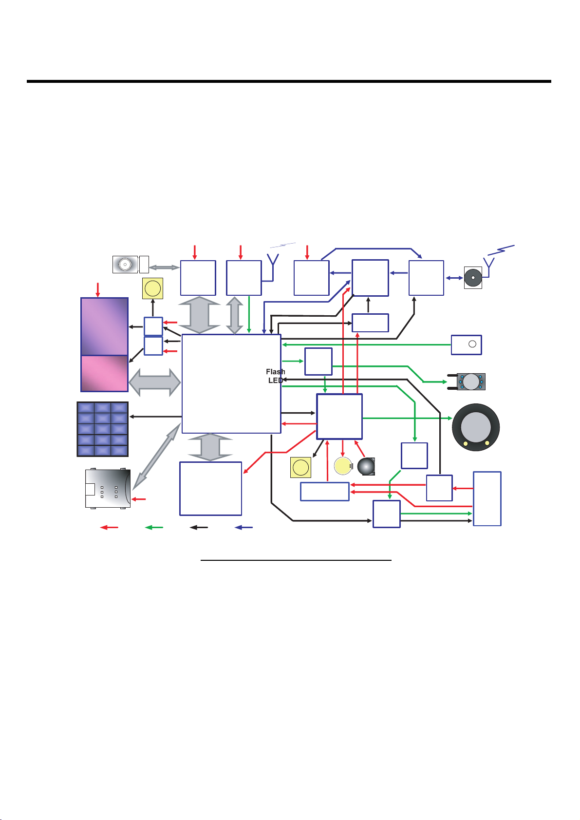
3.1. KF600 Functional Block diagram.
The functional component arrangement is mentioned below diagram.
3. TECHNICAL BRIEF
Figure 2 KF600 Functional block diagram
26M
FM
2î TFT
2î TFT
LCD
LCD
1.5î TFT
1.5î TFT
LCD
LCD
Send
Send
SIM
MICRO SD
C
C
Ext.
Ext.
LDO
LDO
Ext.
LDO
LDO
ISP
MV9319
VBATVBAT
CP
CP
VBATVBAT
BT+FM
BC5
FM
VBATVBATPMICPMICExt.
PAM
SKY77340
26M
RF TR
PMB6272
Hz
FEM
LMSP43QA
BBP
PMB8877
END
END
321
321
654
654
987
987
#0*
#0*
PMICPMIC
PMIC
PMB6821
VIBVIB
SPK
- 20 -
3. TECHNICAL BRIEF
3.2. Baseband Processor (BBP) Introduction
3.2.1. General Description
S-GOLD3™ is a GSM/EDGE single chip mixed signal Baseband IC containing all analog and digital
functionality of a cellular radio. Additionally S-GOLD3™ Provides multimedia extensions such as
camera, software MIDI, MP3 sound. It is designed as a single chip solution, integrating the digital and
mixed signal portions of the base band in 0.09um, 1.2V technology.
The chip will fully support the FR, EFR, HR and AMR-NB vocoding.
S-GOLD3™ support multi-slot operation modes HSCSD (up to class 10), GPRS for high speed data
application (up to class 12) and EGPRS (up to class 12) without additional external hardware.
LGE Internal Use Only
Copyright © 2007 LG Electronics. Inc. All right reserved.
Only for training and service purposes
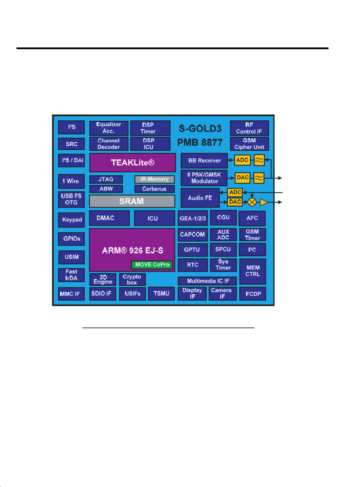
Figure 3 Top level block diagram of the S-GOLD3
™ (PMB8877)

- 21 -
3. TECHNICAL BRIEF
3.2.2. Block Description
• Processing core
ARM926EJ-S 32 bit processor core for controller functions. The ARM926EJ-S includes an MMU,
and the Jazelle Java extension for Java acceleration.
- TEAKLite DSP core
• ARM-Memory
- 32k Byte Boot ROM on the AHB
- 96k Byte SRAM on the AHB, flexibly usable as program or data RAM
- 16k Byte Cache for Program (internal)
- 8k Byte tightly coupled memory for Program(internal)
- 8k Byte Cache for Data(internal)
- 8k Byte tightly coupled memory for Data(internal)
• DSP-Memory
- 104K x 16bit Program ROM
- 8k x 16bit Program RAM
- 60k x 16bit Data ROM
- 37k x 16bit Data RAM
- Incremental Redundancy(IR) Memory of 35904 words of 16bit
• Shared Memory Block
1.5K x 32bit Shared RAM(dual ported) between controller system and TEAKLite.
• Controller Bus system
The processor cores and their peripherals are connected by powerful buses. Multi-layer AHB for
connecting the ARM and the other master capable building blocks with the internal and external
memories and with the peripheral buses.
• Clock system
The clock system allows widely independent selection of frequencies for the essential parts of the
S-GOLD3. Thus power consumption and performance can be optimized for each application.
• Functional Hardware block
- CPU and DSP Timers
- MOVE coprocessor performing motion estimation for video encoding algorithms (H.263, MPEG-4)
- Programmable PLL with additional phase shifters for system clock generation
- GSM Timer Module that off-loads the CPU from radio channel timing
- GMSK / 8-PSK Modulator according to GSM-standard 05.04 (5/2000)
- GMSK Modulator: gauss-filter with B*T=0.3
- EDGE Modulator: 8PSK-modulation with linearized GMSK-Pulse-Filter
- Hardware accelerators for equalizer and channel decoding.
- Incremental Redundancy memory for EDGE class 12 support
- A5/1, A5/2, A5/3 Cipher unit
- GEA1, GEA2, GEA3 Cipher Unit to support GPRS data transmission
LGE Internal Use Only
Copyright © 2007 LG Electronics. Inc. All right reserved.
Only for training and service purposes
- 22 -
3. TECHNICAL BRIEF
- Advanced static and dynamic power management features including TDMA-Frame synchronous
low power mode and enhanced CPU modes(idle and sleep modes)
- Pulse Number Modulation output for Automatic Frequency Correction(AFC)
- Serial RF Control interface: support of direct conversion RF
- A Universal Serial Interface(USIF) enabling asynchronous (UART) of synchronous (SPI) serial
data transmission
- 3 USIF with autobaud detection, hardware flow control and integrated
- A dedicated Fas IfDA Controller supporting IrDA’s SIR,MIR and FIR standards (up to 4Mbps)
- I2C-bus interface (e.g. connection to S/M power)
- A fast display interface supporting serial and parallel interconnection
- An ITU-R BT.656 compatible Camera interface.
- Programmable clock output for a camera
- An multimedia/Secure Digital Card Interface (MMCI/SD: SDIO capable)
3.2.3. External Devices connected to memory interface
Table 1. Memory interface
3.2.4. RF Interface (T_OUT)
S-Gold3 uses this interface to control RF IC and Peripherals. 13 signals are provided switch on/off RF
ICs Periodically each TDMA frame.
Table 2. RF Interface Spec
.
LGE Internal Use Only
Copyright © 2007 LG Electronics. Inc. All right reserved.
Only for training and service purposes
Device Name Maker Remark
FLASH K5E1G12ACA-D075 Samsung Synchronous / A synchronous
DDR K5E1G12ACA-D075 Samsung Synchronous 133MHz
LCD IM200DST2A LGIT 8bit access 2 times transmission
Melody IC Not Used S/W Infineon Software CODEC
T_OUT
Resource Interconnection Description
T_OUT0 TXON_PA PAM Power on
T_OUT1 Other function -
T_OUT2 PA_BAND TX RF band select
T_OUT3 ANT_SW1 FEM control
T_OUT4 ANT_SW2 FEM control
T_OUT5 ANT_SW3 FEM control
T_OUT6 MODE PAM Mode select
- 23 -
3. TECHNICAL BRIEF
3.2.5. USART Interface
KF600 have three USIF Drivers as follow :
- USIF1: Hardware Flow Control / SW upgrade / Calibration
- USIF2: Not used Rx, Tx and CTS, RTS use BT Interface
- USIF3: BT Interface
Table 3. USIF Interface Spec.
3.2.6. ADC channel
BBP ADC block is composed of 7 external ADC channel. This block operates charging process and
other related process by reading battery voltage and other analog values.
Table 4. S-Gold3 ADC channel usage
LGE Internal Use Only
Copyright © 2007 LG Electronics. Inc. All right reserved.
Only for training and service purposes
USIF1
Resource Name Remark
USART0_TXD TXD Transmit Data
USART0_RXD RXD Receive Data
USART0_CTS USB_DP
USART0_RTS USB_DM
USIF2
USART1_TXD NC NC
USART1_RXD NC NC
USART1_CTS BT_CTS
USART1_RTS BT_RTS.
USIF3
USIF3_TXD BT_TX BT Transmit tx
USIF3_RXD BT_RX BT Receive rx
ADC channel
Resource Interconnection Description
M0 BAT_ID Battery temperature measure
M1 RF_TEMP RF block temperature measure
M2 REMOTE_ADC Remote Control
M3 JACK_TYPE Accessory type detect
M4 N.C
M5 N.C
M6 N.C
M7 H/W VERSION S-Gold2 H/W version detect
M8 VSUPPLY Battery supply voltage measure
M9 I_MONITOR Current consumption measure
M10 N.C
- 24 -
3. TECHNICAL BRIEF
3.2.7. GPIO map
Over a hundred allowable resources, KF600 is using as follows except dedicated to SIM and Memory.
KF600 GPIO(General Purpose Input/Output) Map, describing application, I/O state, and enable level,
is shown in below table
Table 5 S-Gold3 GPIO pin Map
LGE Internal Use Only
Copyright © 2007 LG Electronics. Inc. All right reserved.
Only for training and service purposes
Port Function Net Name Description
KEY MATRIX
KP_IN0 KP_IN(0)
KP_IN1 KP_IN(1)
KP_IN2 KP_IN(2)
KP_IN3 KP_IN(3)
KP_IN4 KP_IN(4)
KP_IN5 KP_IN(5)
KP_OUT5 KP_OUT(5)
KP_OUT0 KP_OUT(0)
KP_OUT1 KP_OUT(1)
KP_OUT2 KP_OUT(2)
KP_OUT3 KP_OUT(3)
USIF1
USIF1_RXD RXD UART, RS232 Data
USIF1_TXD TXD UART, RS232 Data
USIF1_RTS_N USB_DP USB Data
USIF1_CTS_N USB_DM USB Data
USIF2
USIF2 _RXD Not used
USIF2 _TXD Not used
USIF2_RTS_N BT_RTS Bluetooth RTS
USIF2_CTS_N BT_CTS Bluetooth CTS
USIF3
USIF3 _RXD BT_RXD Bluetooth RX
USIF3 _TXD BT_TXD Bluetooth TX
- 25 -
3. TECHNICAL BRIEF
LGE Internal Use Only
Copyright © 2007 LG Electronics. Inc. All right reserved.
Only for training and service purposes
CAMERA I/F
CIF_D0 CIF_D(0) Camera DATA[0]
CIF_D1 CIF_D(1) Camera DATA[1]
CIF_D2 CIF_D(2) Camera DATA[2]
CIF_D3 CIF_D(3) Camera DATA[3]
CIF_D4 CIF_D(4) Camera DATA[4]
CIF_D5 CIF_D(5) Camera DATA[5]
CIF_D6 CIF_D(6) Camera DATA[6]
CIF_D7 CIF_D(7) Camera DATA[7]
CIF_PCLK CIF_PCLK Camera pixel clock
CIF_HSYNC CIF_HS Camera H sync
CIF_VSYNC CIF_VS Camera V sync
CLKOUT CIF_MCLK Camera main clock
CIF_PD CIF_PD Camera power down(active high)
CIF_RESET CIF_RESET Camera reset
LCD I/F
DIF_D0 DIF_D(0) LCD data[0]
DIF_D1 DIF_D(1) LCD data[1]
DIF_D2 DIF_D(2) LCD data[2]
DIF_D3 DIF_D(3) LCD data[3]
DIF_D4 DIF_D(4) LCD data[4]
DIF_D5 DIF_D(5) LCD data[5]
DIF_D6 DIF_D(6) LCD data[6]
DIF_D7 DIF_D(7) LCD data[7]
DIF_D8 DIF_D(8) LCD data[8]
DIF_CS1 DIF_MAIN_CS MAIN LCD chip select
DIF_CS2 DIF_SUB_CS SUB LCD chip select
DIF_CD DIF_CD Command Data switch
DIF_WR DIF_WR LCD Write
EINT7 HOOK_DETECT Ear-Mic hook detection
DIF_RESET1 DIF_RESET LCD Reset
GPIO_108 CAM_LDO_EN For CAM Core 1.8V, 2.8V LDO
- 26 -
3. TECHNICAL BRIEF
LGE Internal Use Only
Copyright © 2007 LG Electronics. Inc. All right reserved.
Only for training and service purposes
I2C
I2C_SCL SCL For FM/BT/Amp/Camera
I2C_SDA SDA For FM/BT/Amp/Camera
PM_INT (EINT) PM_INT
SIM I/F
CC_IO SIM_IO SIM CARD I/O
CC_CLK SIM_CLK SIM CARD CLOCK
CC_RST SIM_RST SIM CARD RESET
I2S2
I2S2_CLK0 Not used
GPIO_102 _WP Not used
I2S2_RX Not used
I2S2_TX Not used
I2S2_WA0 Not used
GPIO_103 Not used
External Memory
MMCI_CMD TF_CMD T-flash
MMCI_DAT[0] TF_DAT0 T-flash
MMCI_CLK TF_CLK T-flash
GPIO_109 USB_EOC USB End of charging detect (High: EOC, Low: charging)
IrDA
GPIO_110 RPWRON Remote power on detect (High: Remote, Low: Normal)
GPIO_109 SPK_RCV_SEL Audio pass select(high: Speaker, Low: Receiver)
I2S1
I2S1_CLK0 I2S1_CLK For Bluetooth
GPTU0_0 FLASH_EN For Camera Flash LED
I2S1_RX I2S1_RX For Bluetooth
I2S1_TX I2S1_TX For Bluetooth
I2S1_WA0 I2S1_WA For Bluetooth
External Memory
MMCI_DAT[1] TF_DAT1 T-flash
MMCI_DAT[2] TF_DAT2 T-flash
MMCI_DAT[3] TF_DAT3 T-flash
- 27 -
3. TECHNICAL BRIEF
LGE Internal Use Only
Copyright © 2007 LG Electronics. Inc. All right reserved.
Only for training and service purposes
Audio I/F
EPN1 RCV_N For Receiver
EPP1 RCV_P For Receiver
EPPA1 BBP_SND_L For Speaker
EPREF Reference
EPPA2 BBP_SND_R For Speaker
MICN1 MIC1_N For Mic
MICP1 MIC1_P For Mic
MICN2 MIC2_N For Headset Mic
MICP2 MIC2_P For Headset Mic
VMICP VMICP Power for MIC
VMICN VMICN Power for MIC
ADC
M0 BAT_ID Battery temperature measure
M1 RF_TEMP RF block temperature measure
M2 REMOTE_ADC Remote Control
M3 JACK_TYPE Accessory type detect
M7 H/W VERSION S-Gold2 H/W version detect
M8 VSUPPLY Battery supply voltage measure
M9 I_MONITOR Current consumption measure
M10 N.C
Reference
VREF
IREF
JTAG I/F
TDO TDO JTAG
TDI TDI JTAG
TMS TMS JTAG
TCK TCK JTAG
TRST_n _TRST JTAG
RTCK RTCK JTAG
- 28 -
3. TECHNICAL BRIEF
LGE Internal Use Only
Copyright © 2007 LG Electronics. Inc. All right reserved.
Only for training and service purposes
ETM I/F
TRIG_IN TRIG_IN ETM (Embedded Trace Macro Cell)
MON1 MON1 ETM
MON2 MON2 ETM
TRACESYNC TRACESYNC ETM
TRACECLK TRACECLK ETM
PIPESTAT[2] PIPESTAT2 ETM
PIPESTAT[1] PIPESTAT1 ETM
PIPESTAT[0] PIPESTAT0 ETM
TRACEPKT[0] TRACEPKT(0) ETM
TRACEPKT[1] TRACEPKT(1) ETM
TRACEPKT[2] TRACEPKT(2) ETM
TRACEPKT[3] TRACEPKT(3) ETM
TRACEPKT[4] TRACEPKT(4) ETM
TRACEPKT[5] TRACEPKT(5) ETM
TRACEPKT[6] TRACEPKT(6) ETM
TRACEPKT[7] TRACEPKT(7) ETM
Memory
MEM_AD[0] D(0)
MEM _AD[1] D(1)
MEM _AD[2] D(2)
MEM _AD[3] D(3)
MEM _AD[4] D(4)
MEM _AD[5] D(5)
MEM _AD[6] D(6)
MEM _AD[7] D(7)
MEM _AD[8] D(8)
MEM _AD[9] D(9)
MEM _AD[10] D(10)
MEM _AD[11] D(11)
MEM _AD[12] D(12)
MEM _AD[13] D(13)
MEM _AD[14] D(14)
MEM _AD[15] D(15)
MEM _WR_n _WR
- 29 -
3. TECHNICAL BRIEF
LGE Internal Use Only
Copyright © 2007 LG Electronics. Inc. All right reserved.
Only for training and service purposes
MEM _RD_n _RD
MEM _BC0_n _BC0
MEM _BC1_n _BC1
MEM _A[0] A(0)
MEM _A[1] A(1)
MEM _A[2] A(2)
MEM _A[3] A(3)
MEM _A[4] A(4)
MEM _A[5] A(5)
MEM _A[6] A(6)
MEM _A[7] A(7)
MEM _A[8] A(8)
MEM _A[9] A(9)
MEM _A[10] A(10)
MEM _A[11] A(11)
MEM _A[12] A(12)
MEM _A[13] A(13)
MEM _A[14] A(14)
MEM _A[15] A(15)
MEM _A[16] A(16)
MEM _A[17] A(17)
MEM _A[18] A(18)
MEM _A[19] A(19)
MEM _A[20] A(20)
MEM _A[21] A(21)
MEM _A[22] A(22)
MEM _A[23] A(23)
MEM _A[24] A(24)
MEM _CS0_n _FLASH1_CS INTEL NOR (64MB)
MEM _CS1_n _RAM_CS INTEL SDRAM (64MB)
MEM _CS2_n _FLASH2_CS Not used
MEM _CS3_n _CS3 Not used
MEM _ADV_n _ADV
MEM _RAS_n _RAS
MEM _CAS_n _CAS
- 30 -
3. TECHNICAL BRIEF
LGE Internal Use Only
Copyright © 2007 LG Electronics. Inc. All right reserved.
Only for training and service purposes
MEM _WAIT_n _WAIT
MEM _SDCLKO SDCLKO For Burst mode
MEM _SDCLKI SDCLKI For Burst mode
MEM _BFCLKO BFCLKO For Burst mode
MEM _BFCLKI BFCLKI For Burst mode
MEM _CKE CKE
Memory
FCDP_RBn FCDP
TDMA I/F
T_OUT0 TXON_PA PAM
GPIO_44 VIB_EN
T_OUT2 PA_BAND PAM
T_OUT3 ANT_SW1
T_OUT4 ANT_SW2
T_OUT5 ANT_SW3
T_OUT6 MODE PAM
KP_OUT4 KP_OUT(4)
EINT7 JACK_DETECT
CC1CC3IO LCD_BACKLIGHT LCD Backlight control
GPIO_53 LCD_ID LCD ID check
GPIO_54 _FM_RESET
RF I/F
RF_STR0 RF_EN
CC1CC5IO SLIDE_DETECT Slide on/off detection
RF_DATA RF_DA
RF_CLK RF_CLK
System Port
AFC AFC
CLKOUT0 Not used
[<=26MHz]
- 31 -
3. TECHNICAL BRIEF
LGE Internal Use Only
Copyright © 2007 LG Electronics. Inc. All right reserved.
Only for training and service purposes
F26M 26MHZ_MCLK 26M Main Clock
F32K to 32k crystal
OSC32K to 32k crystal
RESET_n _RESET
TRIG_OUT TRIG_OUT
RTC_OUT RTC_OUT
VCXO_EN VCXO_EN
DSP
GPIO_61 _BT_RESET
GPIO_62 SLED_BACKLIGHT Navi key LED Backlight Control
GPIO_63 _SIM_EN
 Loading...