

Page 1
Service Manual
Date: October, 2008 / Issue 1.0
Service Manual
KF350
Model : KF350
Page 2

LGE Internal Use Only
Copyright © 2008 LG Electronics. Inc. All right reserved.
Only for training and service purposes
- 3 -
* The information in this manual is subject to change without notice and should not be construed as a
commitment by LGE Inc. Furthermore, LGE Inc. reserves the right, without notice, to make changes
to equipment design as advances in engineering and manufacturing methods warrant.
* This manual provides the information necessary to install, program, operate and maintain the KS360
Series.
REVISED HISTORY
Editor Date Issue Contents of Changes S/W Version
J.P.Kim Jul. 18. 2008 0.1 -
Page 3

- 4 -
LGE Internal Use Only
Copyright © 2008 LG Electronics. Inc. All right reserved.
Only for training and service purposes
Page 4

LGE Internal Use Only
Copyright © 2008 LG Electronics. Inc. All right reserved.
Only for training and service purposes
- 5 -
1. INTRODUCTION ..........................7
1.1 Purpose ........................................... 7
1.2 Regulatory Information..................... 7
1.3 ABBREVIATION ............................... 9
2. PERFORMANCE ........................11
2.1 H/W Features ..................................11
2.2 Technical specification ....................12
3. TECHNICAL BRIEF ...................19
3.1 Baseband Processor (BBP)
Introduction......................................19
3.2 Power management IC ...................32
3.3 Power ON/OFF ...............................37
3.4 SIM & uSD interface........................38
3.5 Memory ...........................................40
3.6 LCD Display ....................................41
3.7 Keypad Switching & Scanning ........42
3.8 Keypad back-light illumination.........43
3.9 LCD back-light illumination..............44
3.10 ALC ...............................................46
3.11 JTAG & ETM interface connector..46
3.12 Audio .............................................47
3.13 Charging circuit .............................48
3.14 FM radio & BLUETOOTH..............49
3.15 18pin Multi Media Interface
connector.......................................52
3.16 General Description ......................55
3.17 Receiver part.................................57
3.18 Transmitter part.............................58
3.19 RF synthesizer ..............................59
3.20 DCXO............................................59
3.21 Front End Module control..............60
3.22 Power Amplifier Module ................61
3.23 Mode Selection .............................62
3.24 PAM Schematic .............................63
4. TROUBLE SHOOTING ..............64
4.1 Trouble shooting test setup.............64
4.2 Power on Trouble............................65
4.3 Charging trouble..............................68
4.4 LCD display trouble.........................70
4.5 Camera Troublez.............................72
4.6 Receiver & Speaker troublea ..........74
4.7 Microphone trouble .........................77
4.8 Vibrator trouble................................79
4.9 Keypad back light trouble................81
4.10 SIM & uSD trouble ........................83
4.11 Photo senser trouble .....................86
4.12 sideview LED trouble ....................87
4.13 Trouble shooting of Receiver part .88
4.14 Trouble shooting of Transmitter
part. ...............................................94
5. DOWNLOAD & S/W UPGRADE .103
6. BLOCK DIAGRAM ...................114
7. CIRCUIT DIAGRAM .................115
8. BGA PIN MAP ..........................123
9. PCB LAYOUT ...........................129
10. RF CALIBRATION..................143
10.1 Test Equipment Setup .................143
10.2 Calibration Step...........................143
11. STAND-ALONE TEST ............149
11.1 Test Program Setting...................149
11.2 Tx Test .........................................151
11.3 Rx Test.........................................152
12. EXPLODED VIEW &
REPLACEMENT PART LIST .153
12.1 Exploded View.............................153
12.2 Replacement Parts......................155
12.3 Accessory....................................174
Table Of Contents
Page 5

- 6 -
LGE Internal Use Only
Copyright © 2008 LG Electronics. Inc. All right reserved.
Only for training and service purposes
Page 6

- 7 -
1. INTRODUCTION
1.1 Purpose
This manual provides the information necessary to repair, calibration, description and download the
features of the KF350.
1.2 Regulatory Information
A. Security
Toll fraud, the unauthorized use of telecommunications system by an unauthorized part (for example,
persons other than your company’s employees, agents, subcontractors, or person working on your
company’s behalf) can result in substantial additional charges you’re your telecommunications
services. System users are responsible for the security of own system.
There are may be risks of toll fraud associated with your telecommunications system. System users
are responsible for programming and configuring the equipment to prevent unauthorized use. LGE
does not warrant that this product is immune from the above case but will prevent unauthorized use of
common-carrier telecommunication service of facilities accessed through or connected to it. LGE will
not be responsible for any charges that result from such unauthorized use.
B. Incidence of Harm
If a telephone company determines that the equipment provided to customer is faulty and possibly
causing harm or interruption in service to the telephone network, it should disconnect telephone
service until repair can be done. A telephone company may temporarily disconnect service as long as
repair is not done.
C. Changes in Service
A local telephone company may make changes in its communications facilities or procedure. If these
changes could reasonably be expected to affect the use of the KF350 or compatibility with the network,
the telephone company is required to give advanced written notice to the user, allowing the user to take
appropriate steps to maintain telephone service.
D. Maintenance Limitations
Maintenance limitations on the KF350 must be performed only at the LGE or its authorized agents.
The user may not make any changes and/or repairs expect as specifically noted in this manual.
Therefore, note that unauthorized alternations or repair may affect the regulatory status of the system
and may void any remaining warranty.
1. INTRODUCTION
LGE Internal Use Only
Copyright © 2008 LG Electronics. Inc. All right reserved.
Only for training and service purposes
Page 7

- 8 -
1. INTRODUCTION
E. Notice of Radiated Emissions
The KF350 complies with rules regarding radiation and radio frequency emission as defined by local
regulatory agencies. In accordance with these agencies, you may be required to provide information
such as the following to the end user.
F. Pictures
The pictures in this manual are for illustrative purposes only; your actual hardware may look slightly
different.
G. Interference and Attenuation
An KF350 may interfere with sensitive laboratory equipment, medical equipment, etc. Interference
from unsuppressed engines or electric motors may cause problems.
H. Electrostatic Sensitive Devices
ATTENTION
Boards, which contains Electrostatic Sensitive Device(ESD), are indicated by the sign.
Following information is ESD handling: Service personnel should ground themselves by using a wrist
strap when exchange system boards.
When repairs are made to a system board, they should spread the floor with anti-static mat which is
also grounded. Use a suitable, grounded soldering iron. Keep sensitive parts in these protective
packages until these are used. When returning system boards or parts such as EEPROM to the
factory, use the protective package as described.
LGE Internal Use Only
Copyright © 2008 LG Electronics. Inc. All right reserved.
Only for training and service purposes
Page 8
- 9 -
1. INTRODUCTION
1.3 ABBREVIATION
For the purposes of this manual, following abbreviations apply:
LGE Internal Use Only
Copyright © 2008 LG Electronics. Inc. All right reserved.
Only for training and service purposes
APC Automatic Power Control
BB Baseband
BER Bit Error Ratio
CC-CV Constant Current - Constant Voltage
CLA Cigar Lighter Adapter
DAC Digital to Analog Converter
DCS Digital Communication System
dBm dB relative to 1 milli-watt
DSP Digital Signal Processing
EEPROM Electrical Erasable Programmable Read-Only Memory
EGPRS Enhanced General Packet Radio Service
EL Electroluminescence
ESD Electrostatic Discharge
FPCB Flexible Printed Circuit Board
GMSK Gaussian Minimum Shift Keying
GPIB General Purpose Interface Bus
GPRS General Packet Radio Service
GSM Global System for Mobile Communications
IPUI International Portable User Identity
IF Intermediate Frequency
LCD Liquid Crystal Display
LDO Low Drop Output
LED Light Emitting Diode
Page 9
LGE Internal Use Only
Copyright © 2008 LG Electronics. Inc. All right reserved.
Only for training and service purposes
1. INTRODUCTION
- 10 -
LGE LG Electronics
OPLL Offset Phase Locked Loop
PAM Power Amplifier Module
PCB Printed Circuit Board
PGA Programmable Gain Amplifier
PLL Phase Locked Loop
PSTN Public Switched Telephone Network
RF Radio Frequency
RLR Receiving Loudness Rating
RMS Root Mean Square
RTC Real Time Clock
SAW Surface Acoustic Wave
SIM Subscriber Identity Module
SLR Sending Loudness Rating
SRAM Static Random Access Memory
STMR Side Tone Masking Rating
TA Travel Adapter
TDD Time Division Duplex
TDMA Time Division Multiple Access
UART Universal Asynchronous Receiver/Transmitter
VCO Voltage Controlled Oscillator
DCXO Digitally Controled Crystal Oscillator
WAP Wireless Application Protocol
8PSK 8 Phase Shift Keying
Page 10
- 11 -
2. GENERAL PERFORMANCE
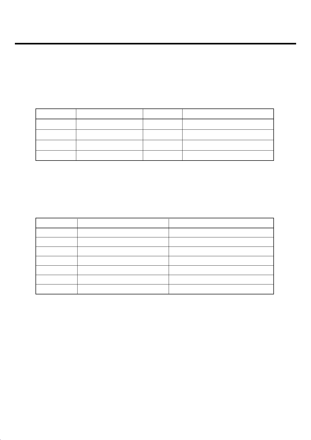
2.1 H/W Feature
2. GENERAL PERFORMANCE
LGE Internal Use Only
Copyright © 2008 LG Electronics. Inc. All right reserved.
Only for training and service purposes
Item Feature Comment
Standard Battery Li-Polymer, 800mAh
AVG TCVR Current 270mA typ @PL5
Standby Current 2.3 mA typ @PP9
Talk time 3 hours (GSM TX Level 7)
Standby time Over 250 hours (Paging Period:9, RSSI: -85dBm)
Charging time Under 3 hours
RX Sensitivity EGSM : -105dBm↓, DCS/PCS: -105dBm↓
TX output power EGSM : 33dBm (@PL 5)
DCS/PCS: 30/29dBm (@PL 0)
GPRS compatibility Class 10
SIM card type 3V Small
Display Main 240 x 320 pixels, 2” QVGA, 262K color
Status Indicator Hard icons. Key Pad
0 ~ 9, #, *, Up/Down/Left/Right/Ok Navigation Key,
Menu Key, Clear Key, Back Key, Confirm Key,
Send Key, Volume Key, PWR Key, Camera Key,
Hot Key
ANT Built in antenna
EAR Phone Jack 18pin multi port Headset jack
PC Synchronization Yes
Speech coding HR/EFR/FR/AMR
Data and Fax Yes
Vibrator Yes
Buzzer No
Voice Recoding Yes
C-Mic Yes
Receiver Yes
Travel Adapter Yes
Options Bluetooth hands-free kit, Data Kit
Page 11
- 12 -
2. GENERAL PERFORMANCE
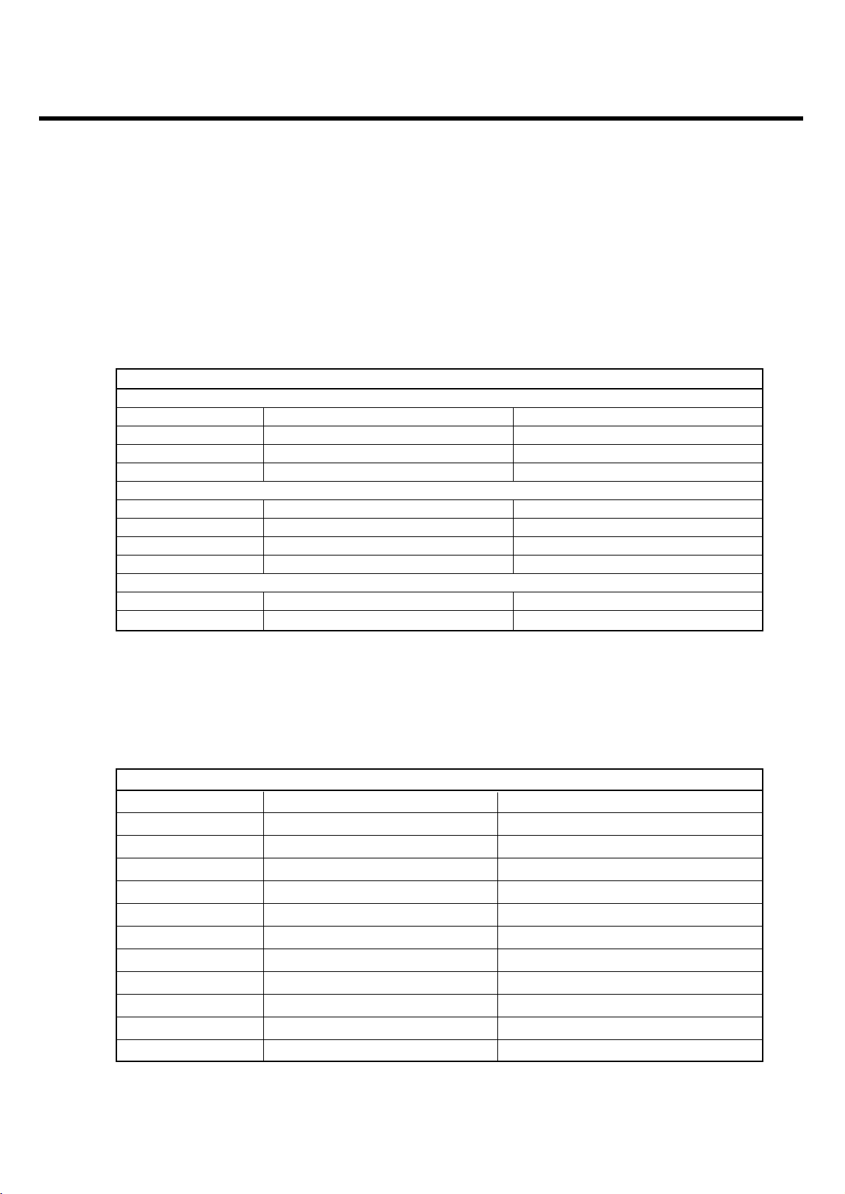
2.2 Technical specification
LGE Internal Use Only
Copyright © 2008 LG Electronics. Inc. All right reserved.
Only for training and service purposes
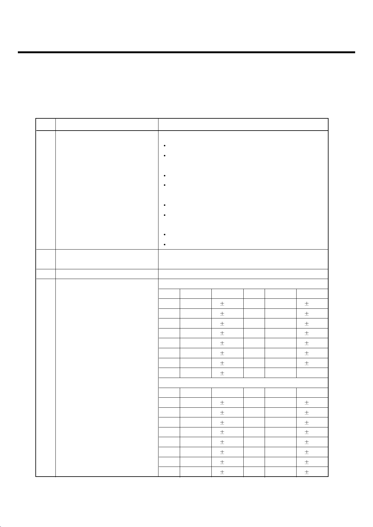
Item Description Specification
GSM900
TX: 890 + 0.2 x n MHz
RX: 935 + 0.2 x n MHz ( n = 1 ~ 124 )
EGSM
TX: 890 + 0.2 x (n-1024) MHz
1Frequency Band
RX: 935 + 0.2 x (n-1024) MHz ( n = 975 ~ 1023 )
DCS1800
TX: 1710 + ( n-511 ) x 0.2 MHz (n = 512 ~ 885)
RX: TX + 95 MHz
PCS1900
TX: 1850.2 + ( n-512 ) x 0.2 MHz (n = 512 ~ 810)
RX: TX + 80MHz
2 Phase Error
RMS < 5 degrees
Peak < 20 degrees
3 Frequency Error < 0.1ppm
GSM900/EGSM
Level Power Toler. Level Power Toler.
5 33 dBm 2dB 13 17 dBm 3dB
6 31 dBm 3dB 14 15 dBm 3dB
7 29 dBm 3dB 15 13 dBm 3dB
8 27 dBm 3dB 16 11 dBm 5dB
9 25 dBm 3dB 17 9 dBm 5dB
10 23 dBm 3dB 18 7 dBm 5dB
11 21 dBm 3dB 19 5 dBm 5dB
12 19 dBm 3dB
4 Power Level DCS1800/PCS1900
Level Power Toler. Level Power Toler.
0 30 dBm 2dB 8 14 dBm 3dB
1 28 dBm 3dB 9 12 dBm 4dB
2 26 dBm 3dB 10 10 dBm 4dB
3 24 dBm 3dB 11 8 dBm 4dB
4 22 dBm 3dB 12 6 dBm 4dB
5 20 dBm 3dB 13 4 dBm 4dB
6 18 dBm 3dB 14 2 dBm 5dB
7 16 dBm 3dB 15 0 dBm 5dB
Page 12
- 13 -
2. GENERAL PERFORMANCE
LGE Internal Use Only
Copyright © 2008 LG Electronics. Inc. All right reserved.
Only for training and service purposes
Item Description Specification
GSM900/EGSM
Offset from Carrier (kHz). Max. dBc
100 +0.5
200 -30
250 -33
400 -60
600 ~ 1,200 -60
1,200 ~ 1,800 -60
1,800 ~ 3,000 -63
3,000 ~ 6,000 -65
5
Output RF Spectrum 6,000 -71
(due to modulation) DCS1800/PCS1900
Offset from Carrier (kHz). Max. dBc
100 +0.5
200 -30
250 -33
400 -60
600 ~ 1,200 -60
1,200 ~ 1,800 -60
1,800 ~ 3,000 -65
3,000 ~ 6,000 -65
6,000 -73
GSM900/EGSM
Offset from Carrier (kHz) Max. (dBm)
Output RF Spectrum 400 -19
6
(due to switching transient) 600 -21
1,200 -21
1,800 -24
Page 13
- 14 -
2. GENERAL PERFORMANCE
LGE Internal Use Only
Copyright © 2008 LG Electronics. Inc. All right reserved.
Only for training and service purposes
Item Description Specification
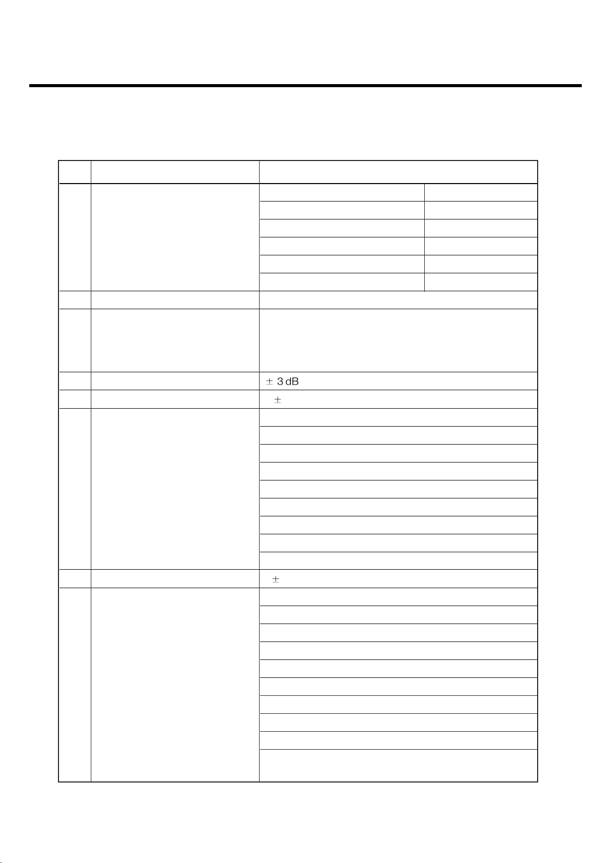
DCS1800/PCS1900
Offset from Carrier (kHz). Max. (dBm)
Output RF Spectrum 400 -22
6
(due to switching transient) 600 -24
1,200 -24
1,800 -27
7 Spurious Emissions Conduction, Emission Status
EGSM
8 Bit Error Ratio
BER (Class II) < 2.439% @-102dBm
DCS1800/PCS1900
BER (Class II) < 2.439% @-100dBm
9 Rx Level Report accuracy
10 SLR 8 3 dB
Frequency (Hz) Max.(dB) Min.(dB)
100 -12 200 0 300 0 -12
11 Sending Response 1,000 0 -6
2,000 4 -6
3,000 4 -6
3,400 4 -9
4,000 0 -
12 RLR 2 3 dB
Frequency (Hz) Max.(dB) Min.(dB)
100 -12 200 0 300 2 -7
500
*
-5
13 Receiving Response 1,000 0 -5
3,000 2 -5
3,400 2 -10
4,000 2
*
Mean that Adopt a straight line in between 300 Hz
and 1,000 Hz to be Max. level in the range.
Page 14
- 15 -
2. GENERAL PERFORMANCE
LGE Internal Use Only
Copyright © 2008 LG Electronics. Inc. All right reserved.
Only for training and service purposes
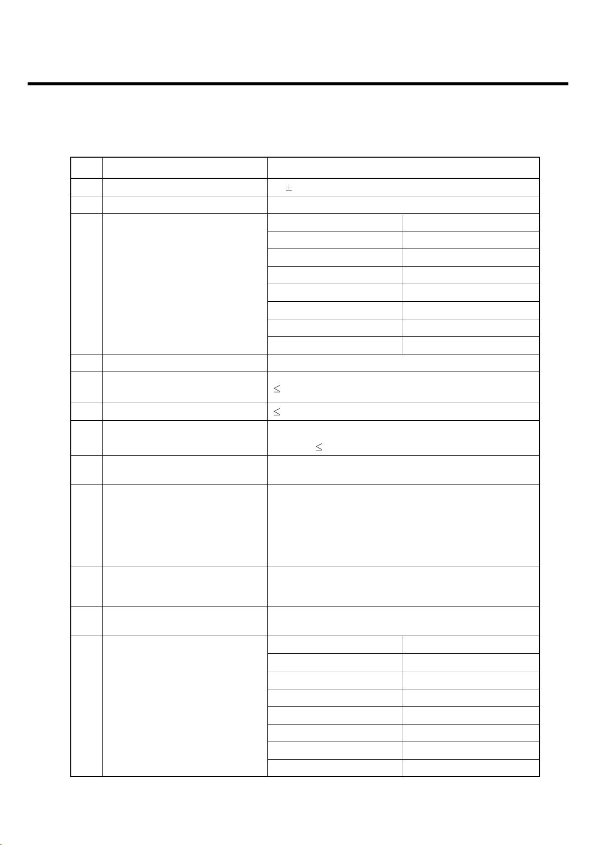
Item Description Specification
14 STMR 13 5 dB
15 Stability Margin > 6 dB
dB to ARL (dB) Level Ratio (dB)
-35 17.5
-30 22.5
-20 30.7
16 Distortion
-10 33.3
0 33.7
7 31.7
10 25.5
17 Side Tone Distortion Three stage distortion < 10%
18
System frequency
2.5ppm
(26 MHz) tolerance
19 32.768KHz tolerance 30ppm
Standby
20 Power consumption
- Normal 3 mA(@PP9)
21 Talk Time
EGSM/Lvl 7 (Battery Capacity 800mA):180 min
EGSM/Lvl12(Battery Capacity 800 mA):320min
Under conditions, at least 300 hours:
1. Brand new and full 800mAh battery
22 Standby Time
2. Full charge, no receive/send and keep GSM in idle mode.
3. Broadcast set off.
4. Signal strength display set at 3 level above.
5. Backlight of phone set off.
At least 65 dB under below conditions:
23 Ringer Volume 1. Ringer set as ringer.
2. Test distance set as 50 cm
24 Charge Current
Fast Charge : < 400 mA
Slow Charge: < 120 mA
Antenna Bar Number Power
7 >-92 dBm ~
7 → 5 -97dBm ~ -93dBm
25 Antenna Display
5 → 4 -100dBm ~ -98dBm
4 → 2 -103dBm ~ -101dBm
2 → 1 -105dBm ~ -104dBm
1 → 0< -106 dBm
Off No Service
Page 15
LGE Internal Use Only
Copyright © 2008 LG Electronics. Inc. All right reserved.
Only for training and service purposes
2. GENERAL PERFORMANCE
- 16 -
Item Description Specification
Battery Bar Number Voltage( 0.05V)
3 4.15V~4.25V
26 Battery Indicator 2 3.69V~3.79V
1 3.62V~3.72V
0 3.54V~3.64V
27 Low Voltage Warning
3.59V ↓ 0.05V (Call)
3.59V ↓ 0.05V (Standby)
28 Forced shut down Voltage 3.23 0.05 V
Li-ion Battery
29 Battery Type
Standard Voltage = 3.7 V
Battery full charge voltage = 4.2 V
Capacity: 800mAh
Switching-mode charger
30 Travel Charger Input: 150 ~ 240 V, 50/60Hz
Out put: 5.1, 0.4A
Page 16
LGE Internal Use Only
Copyright © 2008 LG Electronics. Inc. All right reserved.
Only for training and service purposes
2. GENERAL PERFORMANCE
- 17 -
* EDGE RF Specification (Option: is not serviced for “EDGE mode”)
Item Description Specification
1 RMS EVM 9%
2 Peak EVM 30%
395thPercentile EVM 15%
4Origin Offset Suppression ≥ 30dB
GSM900/EGSM
Level Power Toler. Level Power Toler.
5 27dBm 3dB 13 17dBm 3dB
6 27dBm 3dB 14 15dBm 3dB
7 27dBm 3dB 15 13dBm 3dB
8 27dBm 3dB 16 11dBm 5dB
9 25dBm 3dB 17 9dBm 5dB
10 23dBm 3dB 18 7dBm 5dB
11 21dBm 3dB 19 5dBm 5dB
5 Power Level 12 19dBm 3dB
DCS1800, PCS1900
Level Power Toler. Level Power Toler.
0 26/25dBm 3dB 8 14 dBm 3dB
1 26/25dBm 3dB 9 12 dBm 4dB
2 26/25dBm 3dB 10 10 dBm 4dB
3 24 dBm 3dB 11 8 dBm 4dB
4 22 dBm 3dB 12 6 dBm 4dB
5 20 dBm 3dB 13 4 dBm 4dB
6 18 dBm 3dB 14 2 dBm 5dB
7 16 dBm 3dB 15 0 dBm 5dB
6 Output RF Spectrum GSM900/EGSM
(due to modulation) Offset from carrier(kHz) Max. dBc
100 +0.5
200 -30
250 -33
400 -54
600 ~ <1,200 -60
1,200 ~ <1,800 -60
1,800 ~ <3,000 -63
3,000 ~ <6,000 -65
6,000 -71
Page 17
LGE Internal Use Only
Copyright © 2008 LG Electronics. Inc. All right reserved.
Only for training and service purposes
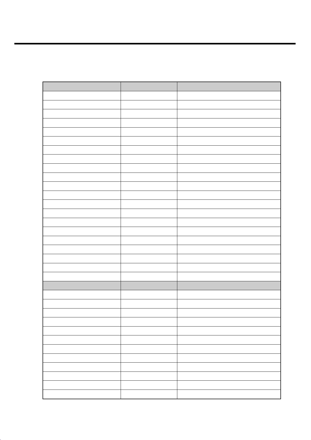
2. GENERAL PERFORMANCE
- 18 -
Item Description Specification
6 Output RF Spectrum DCS1800, PCS1900
(due to modulation) Offset from carrier(kHz) Max. dBc
100 +0.5
200 -30
250 -33
400 -54
600 ~ <1,200 -60
1,200 ~ <1,800 -60
1,800 ~ <3,000 -63
3,000 ~ <6,000 -65
6,000 -71
7 Output RF Spectrum GSM900/EGSM
(due to switching transient) Offset from carrier(kHz) Max. dBm
400 -23
600 -26
1,200 -27
1,800 --30
DCS1800, PCS1900
Offset from carrier(kHz) Max. dBm
400 -23
600 -26
1,200 -27
1,800 -30
Page 18
LGE Internal Use Only
Copyright © 2008 LG Electronics. Inc. All right reserved.
Only for training and service purposes
3. TECHNICAL BRIEF
- 19 -
3.1 Baseband Processor (BBP) Introduction
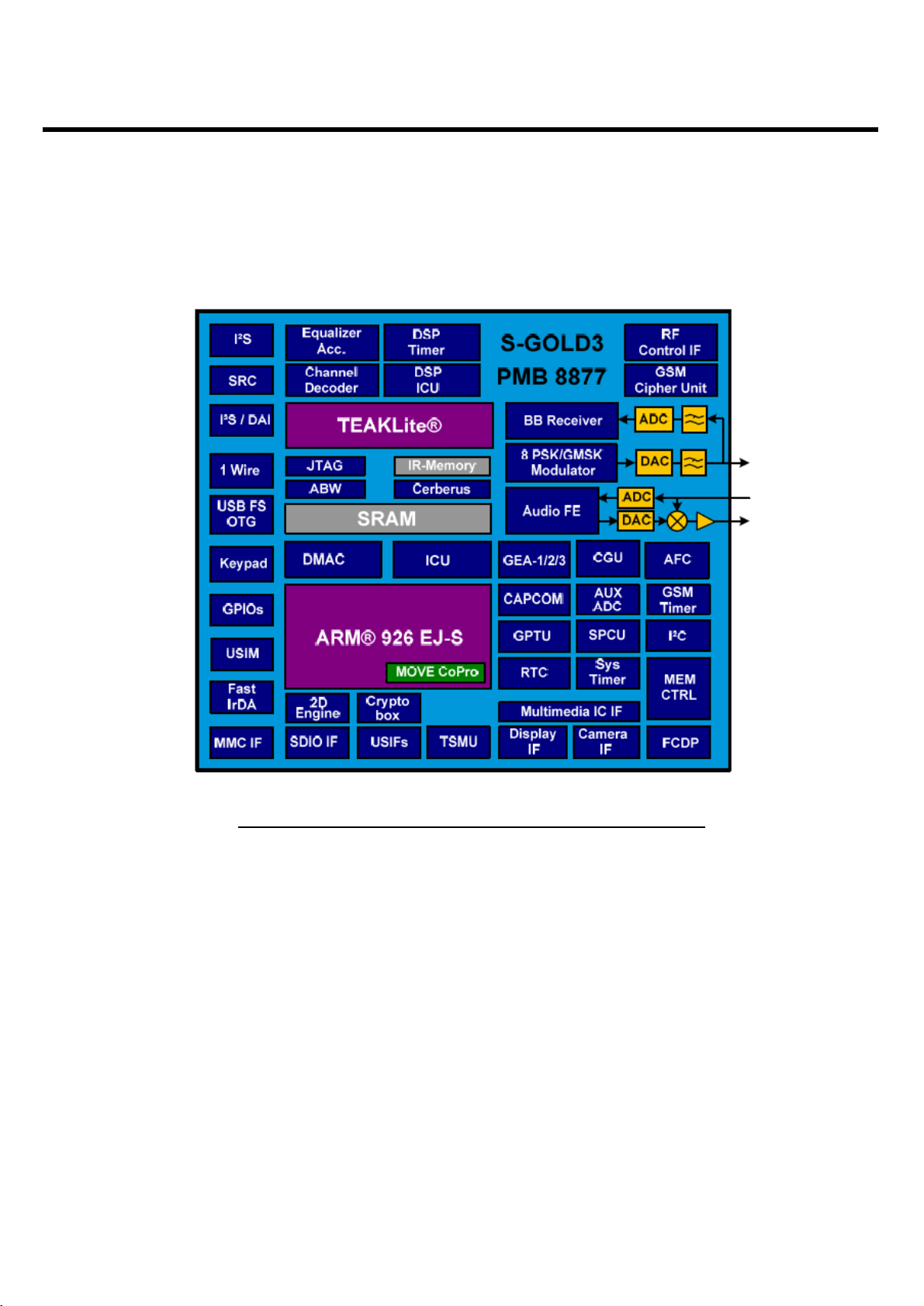
3. TECHNICAL BRIEF
Figure 1 Top level block diagram of the S-GOLD3TM (PMB8877)
Page 19

- 20 -
3. TECHNICAL BRIEF
3.1.1 General Description
S-GOLD3TMis a GSM/EDGE single chip mixed signal Baseband IC containing all analog and digital
functionality of a cellular radio. Additionally S-GOLD3TMProvides multimedia extensions such as
camera, software MIDI, MP3 sound. It is designed as a single chip solution, integrating the digital and
mixed signal portions of the base band in 0.09um, 1.2V technology.
The chip will fully support the FR, EFR, HR and AMR-NB vocoding. S-GOLD3TMsupport multi-slot
operation modes HSCSD (up to class 10), GPRS for high speed data application (up to class 12) and
EGPRS (up to class 12) without additional external hardware.
3.1.2 Block Description
• Processing core
ARM926EJ-S 32 bit processor core for controller functions. The ARM926EJ-S includes an MMU,
and the Jazelle Java extension for Java acceleration.
- TEAKLite DSP core
• ARM-Memory
- 32k Byte Boot ROM on the AHB
- 96k Byte SRAM on the AHB, flexibly usable as program or data RAM
- 16k Byte Cache for Program (internal)
- 8k Byte tightly coupled memory for Program(internal)
- 8k Byte Cache for Data(internal)
- 8k Byte tightly coupled memory for Data(internal)
• DSP-Memory
- 104K x 16bit Program ROM
- 8k x 16bit Program RAM
- 60k x 16bit Data ROM
- 37k x 16bit Data RAM
- Incremental Redundancy(IR) Memory of 35904 words of 16bit
LGE Internal Use Only
Copyright © 2008 LG Electronics. Inc. All right reserved.
Only for training and service purposes
Page 20

- 21 -
3. TECHNICAL BRIEF
• Shared Memory Block
1.5K x 32bit Shared RAM(dual ported) between controller system and TEAKLite.
• Controller Bus system
The processor cores and their peripherals are connected by powerful buses. Multi-layer AHB for
connecting the ARM and the other master capable building blocks with the internal and external
memories and with the peripheral buses.
• Clock system
The clock system allows widely independent selection of frequencies for the essential parts of the
S-GOLD3. Thus power consumption and performance can be optimized for each application.
• Functional Hardware block
- CPU and DSP Timers
- MOVE coprocessor performing motion estimation for video encoding algorithms
(H.263, MPEG-4)
- Programmable PLL with additional phase shifters for system clock generation
- GSM Timer Module that off-loads the CPU from radio channel timing
- GMSK / 8-PSK Modulator according to GSM-standard 05.04 (5/2000)
- GMSK Modulator: gauss-filter with B*T=0.3
- EDGE Modulator: 8PSK-modulation with linearized GMSK-Pulse-Filter
- Hardware accelerators for equalizer and channel decoding.
- Incremental Redundancy memory for EDGE class 12 support
- A5/1, A5/2, A5/3 Cipher unit
- GEA1, GEA2, GEA3 Cipher Unit to support GPRS data transmission
- Advanced static and dynamic power management features including TDMA-Frame synchronous
low power mode and enhanced CPU modes(idle and sleep modes)
- Pulse Number Modulation output for Automatic Frequency Correction(AFC)
- Serial RF Control interface: support of direct conversion RF
- A Universal Serial Interface(USIF) enabling asynchronous (UART) of synchronous (SPI) serial
data transmission
- 3 USIF with autobaud detection, hardware flow control and integrated
- A dedicated Fas IfDA Controller supporting IrDA’s SIR,MIR and FIR standards (up to 4Mbps)
- I2C-bus interface (e.g. connection to S/M power)
- A fast display interface supporting serial and parallel interconnection
- An ITU-R BT.656 compatible Camera interface.
- Programmable clock output for a camera
- An multimedia/Secure Digital Card Interface (MMCI/SD:SDIO capable)
LGE Internal Use Only
Copyright © 2008 LG Electronics. Inc. All right reserved.
Only for training and service purposes
Page 21
- 22 -
3. TECHNICAL BRIEF
3.1.3 External Devices connected to memory interface
Table 1. Memory interface
3.1.4 RF Interface (T_OUT)
S-Gold3 uses this interface to control RF IC and Peripherals. 13 signals are provided switch on/off RF
ICs Periodically each TDMA frame.
Table 2. RF Interface Spec.
LGE Internal Use Only
Copyright © 2008 LG Electronics. Inc. All right reserved.
Only for training and service purposes
Device Name Maker Remark
FLASH K5E1G12ACA-D075 Samsung Synchronous / A synchronous
DDR K5E1G12ACA-D075 Samsung Synchronous 133MHz
LCD IM200DST2A LGIT 8bit access 2 times transmission
Melody IC Not Used S/W Infineon Software CODEC
Resource Interconnection Description
T_OUT0 TXON_PA PAM Power on
T_OUT1 Other function -
T_OUT2 PA_BAND TX RF band select
T_OUT3 ANT_SW1 FEM control
T_OUT4 ANT_SW2 FEM control
T_OUT5 ANT_SW3 FEM control
T_OUT6 MODE PAM Mode select
Page 22
- 23 -
3. TECHNICAL BRIEF
3.1.5 USIF Interface
KF350 have three USIF Drivers as follow :
- USIF1 : Hardware Flow Control / SW upgrade / Calibration
- USIF2 : Not used Rx, Tx and CTS, RTS use BT Interface
- USIF3 : BT Interface
Table 3. USIF Interface Spec.
3.1.6 ADC channel
BBP ADC block is composed of 10 external ADC channel. This block operates charging process and
other related process by reading battery voltage and other analog values.
Table 4. S-Gold3 ADC channel usage
LGE Internal Use Only
Copyright © 2008 LG Electronics. Inc. All right reserved.
Only for training and service purposes
Resource Name Remark
USIF1
USIF1_TXD TXD Transmit Data
USIF1_RXD RXD Receive Data
USIF1_CTS USB_DP
USIF1_RTS USB_DM
USIF2
USIF2_TXD NC NC
USIF2_RXD NC NC
USIF2_CTS BT_CTS
USIF2_RTS BT_RTS.
USIF3
USIF3_TXD BT_TX BT Transmit tx
USIF3_RXD BT_RX BT Receive rx
ADC channel
Resource Interconnection Description
M0 BAT_ID Battery temperature measure
M1 RF_TEMP RF block temperature measure
M2 N.C
M3 JACK_TYPE Accessory type detect
M4 N.C
M5 H/W VERSION S-Gold3 H/W version detect
M6 N.C
M7 N.C
M8 VSUPPLY Battery supply voltage measure
M9 N.C
M10 N.C
Page 23
3.1.7 GPIO map
Over a hundred allowable resources, KF350 is using as follows except dedicated to SIM and Memory.
KF350 GPIO(General Purpose Input/Output) Map, describing application, I/O state, and enable level,
is shown in below table
Table 5 S-Gold3 GPIO pin Map
- 24 -
3. TECHNICAL BRIEF
LGE Internal Use Only
Copyright © 2008 LG Electronics. Inc. All right reserved.
Only for training and service purposes
Port Function Net Name Description
KEY MATRIX
KP_IN0 KP_IN(0)
KP_IN1 KP_IN(1)
KP_IN2 KP_IN(2)
KP_IN3 KP_IN(3)
KP_IN4 KP_IN(4)
KP_IN5 KP_IN(5)
KP_OUT5 KP_OUT(5)
KP_OUT0 KP_OUT(0)
KP_OUT1 KP_OUT(1)
KP_OUT2 KP_OUT(2)
KP_OUT3 KP_OUT(3)
USIF1
USIF1_RXD RXD UART, RS232 Data
USIF1_TXD TXD UART, RS232 Data
USIF1_RTS_N USB_DP USB Data
USIF1_CTS_N USB_DM USB Data
USIF2
USIF2 _RXD Not used
USIF2 _TXD Not used
USIF2_RTS_N BT_RTS Bluetooth RTS
USIF2_CTS_N BT_CTS Bluetooth CTS
USIF3
USIF3 _RXD BT_RXD Bluetooth RX
USIF3 _TXD BT_TXD Bluetooth TX
CLK
CLK32K CLK32k For FM Radio, BT CLK32K
GPIO_22 Not used
Page 24
- 25 -
3. TECHNICAL BRIEF
LGE Internal Use Only
Copyright © 2008 LG Electronics. Inc. All right reserved.
Only for training and service purposes
CAMERA I/F
CIF_PCLK CAM_PCLK Camera pixel clock
CIF_HSYNC CAM_HS Camera H sync
CIF_VSYNC CAM_VS Camera V sync
CLKOUT2 CAM_MCLK Camera main clock
CIF_PD_GPIO CAM_PWDN Camera sensor power down
CIF_RESET_GPIO CAM_RST Camera reset
#Display_Interface
CIF_D0 CIF_D(0) Camera DATA[0]
CIF_D1 CIF_D(1) Camera DATA[1]
CIF_D2 CIF_D(2) Camera DATA[2]
CIF_D3 CIF_D(3) Camera DATA[3]
CIF_D4 CIF_D(4) Camera DATA[4]
CIF_D5 CIF_D(5) Camera DATA[5]
CIF_D6 CIF_D(6) Camera DATA[6]
CIF_D7 CIF_D(7) Camera DATA[7]
CIF_PCLK CIF_PCLK Camera pixel clock
CIF_HSYNC CIF_HS Camera H sync
CIF_VSYNC CIF_VS Camera V sync
CLKOUT CIF_MCLK Camera main clock
CIF_PD CIF_PD Camera power down(active high)
CIF_RESET CIF_RESET Camera reset
LCD I/F
DIF_D0 DIF_D(0) LCD data[0]
DIF_D1 DIF_D(1) LCD data[1]
DIF_D2 DIF_D(2) LCD data[2]
DIF_D3 DIF_D(3) LCD data[3]
DIF_D4 DIF_D(4) LCD data[4]
DIF_D5 DIF_D(5) LCD data[5]
DIF_D6 DIF_D(6) LCD data[6]
DIF_D7 DIF_D(7) LCD data[7]
DIF_D8 DIF_D(8) LCD data[8]
DIF_CS1 DIF_MAIN_CS MAIN LCD chip select
DIF_CS2 DIF_SUB_CS SUB LCD chip select
DIF_CD DIF_CD Command Data switch
Page 25
- 26 -
3. TECHNICAL BRIEF
LGE Internal Use Only
Copyright © 2008 LG Electronics. Inc. All right reserved.
Only for training and service purposes
DIF_WR DIF_WR LCD Write
EINT7 HOOK_DETECT Ear-Mic hook detection
DIF_RESET1 DIF_RESET LCD Reset
GPIO_108 CAM_LDO_EN For CAM Core 1.8V, 2.8V LDO
I2C
I2C_SCL SCL For FM/BT/Amp/Camera
I2C_SDA SDA For FM/BT/Amp/Camera
PM_INT (EINT) PM_INT
SIM I/F
CC_IO SIM_IO SIM CARD I/O
CC_CLK SIM_CLK SIM CARD CLOCK
CC_RST SIM_RST SIM CARD RESET
I2S2
I2S2_CLK0 Not used
GPIO_102 _WP Not used
I2S2_RX Not used
I2S2_TX Not used
I2S2_WA0 Not used
GPIO_103 Not used
External Memory
MMCI_CMD TF_CMD T-flash
MMCI_DAT[0] TF_DAT0 T-flash
MMCI_CLK TF_CLK T-flash
GPIO_109 USB_EOC USB End of charging detect
(High: EOC, Low: charging)
IrDA
GPIO_110 RPWRON Remote power on detect
(High: Remote, Low: Normal)
GPIO_109 SPK_RCV_SEL Audio pass select
(high: Speaker, Low: Receiver)
I2S1
I2S1_CLK0 I2S1_CLK For Bluetooth
GPTU0_0 FLASH_EN For Camera Flash LED
I2S1_RX I2S1_RX For Bluetooth
I2S1_TX I2S1_TX For Bluetooth
I2S1_WA0 I2S1_WA For Bluetooth
Page 26
External Memory
MMCI_DAT[1] TF_DAT1 T-flash
MMCI_DAT[2] TF_DAT2 T-flash
MMCI_DAT[3] TF_DAT3 T-flash
Audio I/F
EPN1 RCV_N For Receiver
EPP1 RCV_P For Receiver
EPPA1 BBP_SND_L For Speaker
EPREF Reference
EPPA2 BBP_SND_R For Speaker
MICN1 MIC1_N For Mic
MICP1 MIC1_P For Mic
MICN2 MIC2_N For Headset Mic
MICP2 MIC2_P For Headset Mic
VMICP VMICP Power for MIC
VMICN VMICN Power for MIC
ADC
M0 BAT_ID Battery temperature measure
M1 RF_TEMP RF block temperature measure
M2 REMOTE_ADC Remote Control
M3 JACK_TYPE Accessory type detect
M7 H/W VERSION S-Gold2 H/W version detect
M8 VSUPPLY Battery supply voltage measure
M9 I_MONITOR Current consumption measure
M10 N.C
Reference
VREF
IREF
JTAG I/F
TDO TDO JTAG
TDI TDI JTAG
TMS TMS JTAG
TCK TCK JTAG
TRST_n _TRST JTAG
RTCK RTCK JTAG
- 27 -
3. TECHNICAL BRIEF
LGE Internal Use Only
Copyright © 2008 LG Electronics. Inc. All right reserved.
Only for training and service purposes
Page 27
- 28 -
3. TECHNICAL BRIEF
LGE Internal Use Only
Copyright © 2008 LG Electronics. Inc. All right reserved.
Only for training and service purposes
ETM I/F
TRIG_IN TRIG_IN ETM (Embedded Trace Macro Cell)
MON1 MON1 ETM
MON2 MON2 ETM
TRACESYNC TRACESYNC ETM
TRACECLK TRACECLK ETM
PIPESTAT[2] PIPESTAT2 ETM
PIPESTAT[1] PIPESTAT1 ETM
PIPESTAT[0] PIPESTAT0 ETM
TRACEPKT[0] TRACEPKT(0) ETM
TRACEPKT[1] TRACEPKT(1) ETM
TRACEPKT[2] TRACEPKT(2) ETM
TRACEPKT[3] TRACEPKT(3) ETM
TRACEPKT[4] TRACEPKT(4) ETM
TRACEPKT[5] TRACEPKT(5) ETM
TRACEPKT[6] TRACEPKT(6) ETM
TRACEPKT[7] TRACEPKT(7) ETM
Memory
MEM_AD[0] D(0)
MEM _AD[1] D(1)
MEM _AD[2] D(2)
MEM _AD[3] D(3)
MEM _AD[4] D(4)
MEM _AD[5] D(5)
MEM _AD[6] D(6)
MEM _AD[7] D(7)
MEM _AD[8] D(8)
MEM _AD[9] D(9)
MEM _AD[10] D(10)
MEM _AD[11] D(11)
MEM _AD[12] D(12)
MEM _AD[13] D(13)
MEM _AD[14] D(14)
MEM _AD[15] D(15)
MEM _WR_n _WR
Page 28
- 29 -
3. TECHNICAL BRIEF
LGE Internal Use Only
Copyright © 2008 LG Electronics. Inc. All right reserved.
Only for training and service purposes
MEM _RD_n _RD
MEM _BC0_n _BC0
MEM _BC1_n _BC1
MEM _A[0] A(0)
MEM _A[1] A(1)
MEM _A[2] A(2)
MEM _A[3] A(3)
MEM _A[4] A(4)
MEM _A[5] A(5)
MEM _A[6] A(6)
MEM _A[7] A(7)
MEM _A[8] A(8)
MEM _A[9] A(9)
MEM _A[10] A(10)
MEM _A[11] A(11)
MEM _A[12] A(12)
MEM _A[13] A(13)
MEM _A[14] A(14)
MEM _A[15] A(15)
MEM _A[16] A(16)
MEM _A[17] A(17)
MEM _A[18] A(18)
MEM _A[19] A(19)
MEM _A[20] A(20)
MEM _A[21] A(21)
MEM _A[22] A(22)
MEM _A[23] A(23)
MEM _A[24] A(24)
MEM _CS0_n _FLASH1_CS INTEL NOR (64MB)
MEM _CS1_n _RAM_CS INTEL SDRAM (64MB)
MEM _CS2_n _FLASH2_CS Not used
MEM _CS3_n _CS3 Not used
MEM _ADV_n _ADV
MEM _RAS_n _RAS
MEM _CAS_n _CAS
Page 29
- 30 -
3. TECHNICAL BRIEF
LGE Internal Use Only
Copyright © 2008 LG Electronics. Inc. All right reserved.
Only for training and service purposes
MEM _WAIT_n _WAIT
MEM _SDCLKO SDCLKO For Burst mode
MEM _SDCLKI SDCLKI For Burst mode
MEM _BFCLKO BFCLKO For Burst mode
MEM _BFCLKI BFCLKI For Burst mode
MEM _CKE CKE
Memory
FCDP_RBn FCDP
TDMA I/F
T_OUT0 TXON_PA PAM
GPIO_44 VIB_EN
T_OUT2 PA_BAND PAM
T_OUT3 ANT_SW1
T_OUT4 ANT_SW2
T_OUT5 ANT_SW3
T_OUT6 MODE PAM
KP_OUT4 KP_OUT(4)
EINT7 JACK_DETECT
CC1CC3IO LCD_BACKLIGHT LCD Backlight control
GPIO_53 LCD_ID LCD ID check
GPIO_54 _FM_RESET
RF I/F
RF_STR0 RF_EN
CC1CC5IO SLIDE_DETECT Folder on/off detection
RF_DATA RF_DA
RF_CLK RF_CLK
System Port
AFC AFC
CLKOUT0 [<=26MHz] Not used
F26M 26MHZ_MCLK 26M Main Clock
F32K to 32k crystal
OSC32K to 32k crystal
RESET_n _RESET
TRIG_OUT TRIG_OUT
RTC_OUT RTC_OUT
Page 30
- 31 -
3. TECHNICAL BRIEF
LGE Internal Use Only
Copyright © 2008 LG Electronics. Inc. All right reserved.
Only for training and service purposes
VCXO_EN VCXO_EN
DSP
GPIO_61 _BT_RESET
GPIO_62 SLED_BACKLIGHT Navi key LED Backlight Control
GPIO_63 _SIM_EN
Page 31

- 32 -
3. TECHNICAL BRIEF
3.2 Power management IC
3.2.1 General Description
SM-POWER is a highly integrated Power and Battery Management IC for mobile handsets. It has
been specially designed for usage with S-Gold3. Although optimized for usage with the Infineon SGOLD baseband device it is suitable for the S-GOLDlite and the E-GOLD+ baseband devices as
well. It also supports the cellular RF devices like SMARTi-DC, SMARTi-DC+, SMARTi-SD and the
Bluemoon Single, Infineon’s single chip solution for Bluetooth. If used with S-GOLD3 it provides all
power supply functions (except for the RF PA) for a complete advanced GSM Edge smart phone
minimizing external device count.
Block Description
• Highly efficient step-down converter for main digital baseband supply including Core, DSP and
memory interface (External Bus Unit).
• Support of S-GOLD standby power-down concept
• Low-drop-out (LDO) regulators for Flash and mobile RAM memory devices
• Voltage independent switching of two SIM cards
• LDO regulators for baseband I/O supply
• LDO regulator for analog mixed-signal section of S-GOLD
• Low-noise LDO regulators for RF devices
• Supply for Bluemoon Single, Infineon’s single chip solution for Bluetooth
• Audio amplifier 8 Ohms for handsfree operation and ringing
• Charge Control for charging Li-Ion/Polymer batteries under software control
• Pre-charge current generator with selectable current level
• RTC regulator with ultra-low quiescent current
• USB interface support for peripheral and mini-host mode
• Backlight LEDs driver with current selection and PWM dimming function
• Two single LED driver outputs for signaling
• Vibrator driver with adjustable voltage
• Fully controlable by software via I2C - Bus
• Temperature and battery voltage sensors
• Interrupt channels for peripherals
• System debug mode
• VQFN 48 package with heat sink and non-protruding leads
• Compatible with the Infineon E-GOLD+ V2 and V3
LGE Internal Use Only
Copyright © 2008 LG Electronics. Inc. All right reserved.
Only for training and service purposes
Page 32

- 33 -
3. TECHNICAL BRIEF
SM-POWER is a further step on the successful E-Power product line with enhanced and optimized
functionality.
SM-POWER features a baseband supply concept with a DC/DC step-down converter cascaded by
two linear regulators
- SM-POWER’s DC/DC converter makes up to 40 % reduction of battery current for smart phone
functions (e.g. organizer functions, games, MP3 decoding) possible.
- SDBB has high efficiency up to 95% and also a power save mode.
- Memory Interface is directly supported by the SDBB
- SDBB can also act as main supply voltage for E-GOLD+ or S-GOLDlite baseband devices.
- For S-GOLD two linear regulators for DSP and Core are cascaded after the SDBB.
SM-POWER supports the standby power-down concept of S-GOLD by temporarily switching off the
linear regulator for the DSP during mobile standby whenever this subsystem is not used. In this
phase the ARM controller and most peripherals including parts of the on-chip SRAM are kept
powered-up with power being supplied by the other linear regulator.
SM-POWER includes a fully differential audio amplifier able to drive loads down to a nominal value
of 8 Ohm for usage in hands-free phones and for ringing
- 450 mW maximum output power
- adjustable gain
- mute switch SM-POWER also integrates a charging function for Li-Ion, Li-Polymer batteries
- click and pop -protection SM-POWER also integrates a charging function for Li-Ion, Li-Polymer
batteries
- Precharge current source with two current levels
- Constant current / constant voltage charging with 3 different termination voltages
- Programable charge current limitation for use with different batteries
- Freely programable pulse charging to reduce the thermal power dissipation in the constant voltage
charging phase
- Top-off charge current sensing SM-POWER completes the USB interface of S-GOLD
- Regulated voltage for S-GOLD USB interface including reverse current and overvoltage protection
- Switch to supply USB pull-up resistor
- Mini-host pull down resistor functionality
- Charge pump with internal switching capacitor for USB host VBUS supply voltage SM-POWER
fully supports LED and Vibra Motor functionality
- no external components needed
- driver for backlight LEDs adjustable in steps up to 140mA and with soft turn on and off by PWM
dimming
- two driver outputs for single LEDs for precharge indication and signaling with i.e. change of colour
LGE Internal Use Only
Copyright © 2008 LG Electronics. Inc. All right reserved.
Only for training and service purposes
Page 33

- driver for Vibra Motor with adjustable voltages, soft startup / shutdown and current limitation SMPOWER offers several control functions
- Power-on Reset Generator with logic state machine
- I2C bus interface
- I2C bus configurable mode control logic with ON (push-button or RTC), VCXOEN and LRF3EN
(wake-up by Bluetooth) inputs
- Programable interrupt channels to handle peripherals like SIM, MMC and USB
- Monitoring of charging functions
- Undervoltage Shut-Down
- Errorflags (volatile or non-volatile) from many power-supply functions and thermal sensor in order
to debug system
- Overtemperature Shut-Down
- Overtemperature Warning
- Support of S-GOLD standby power-down concept
- Support of S-GOLD Power-Down Pad Tristate Function
Table 6. LDO Output Table of SM-Power
- 34 -
3. TECHNICAL BRIEF
LGE Internal Use Only
Copyright © 2008 LG Electronics. Inc. All right reserved.
Only for training and service purposes
LDO Net name Output Voltage Output Current Usage
SD1 1V35_Core 1.35V 600mA Core & for LDO
SD2 1V8_SD 1.8V 300mA Memory
VAUX 2V9_VAF 2.9V 100mA Cam Auto Focus
VIO 2V62_VIO 2.62V 100mA Peripherals
VSIM 2V9_SIM 2.9V 70mA SIM card
VMME 2V8_VMME 2.9V 150mA u-SD
VUMTS 2V85_AMP 2.85V 110mA Headset AMP
VUSB VUSB 3.1V 40mA Not used
VLED VLED 2.9V 10mA Not used
VAUDIOa 2V5_VAUDA 2.5V 200mA Stereo headset, Mono earpiece
VAUDIOb 2V5_VAUDB 2.5V 50mA Analog parts of S-Gold
VRF1 2V85_VRF 2.85V 150mA 2.85 V supply for SMARTi-PM
RF transceiver
VRF2 1V5_VRF 1,53V 100mA 1.5 V supply for SMARTi-PM
RF transceiver
VRF3 2V65_VBT 2.7V 150mA Bluetooth
VPLL 1V35_VPLL 1.35V 30mA S-GOLD3 PLL
VRTC 2V11_RTC 2.11V 4mA Real Time Clock
VAFC VAFC 2.65V 5mA Not used
VVIB 2V8_VLCD 2.8V 140mA LCD
Page 34

- 35 -
3. TECHNICAL BRIEF
LGE Internal Use Only
Copyright © 2008 LG Electronics. Inc. All right reserved.
Only for training and service purposes
Figure 3. SM-Power Circuit Diagram of KF350
Figure 4 SM-Power circuit diagram with charging part
PMIC
1V8_SD
CN201
G1
G2
1V35_VPLL
KEY_EN
B10
C9
FLASH_ON
VSS11
E8
E9
TXONPA
VSS12
R201
27K
R202
DNI
VBAT
VBAT
2V62_VIO
1u
4.7KR203
2.2uC207
2.2uC208
C206
R205 4.7K
R204 4.7K
TP201
L1
A11
J4
A1
B4
B11
B9
A10
VIO
VPLL
VSD2
PUMS1
PUMS2
PUMS3
OUTPORT
VDDPLLIO
U202
PMB6821
VSS22G6VSS23
VSS13
F3
F4
VSS24
VSS14
VSS15
VSS16
VSS17
VSS18
VSS19
VSS20
VSS21
F5
F6
F7
F8
F9
G4
G5
G7
G3
K3
L3
POWER_ON
VSS25
G8
G9
WDOG
WDOG
VSS26
K4
H5
PWRON
L4
ON_OFF1
VSS27
H6
ON_OFF2
L5
ON_OFF2
ON_OFF_OUT
VSS28
VSS29
H7
J5
J6
SDA
SPOWER_INT
RESOURCE_CTRL
SCL
SP_INT
J7
K6
K5
I2C_INT
I2C_CLK
I2C_DAT
RESOURCE_CRTL
VSS30
D9
2V62_VIO
R206 4.7K
VSS_SD1
H8
4.7KR207
L6
K7
BL1_PWM
VSS_SD2H4VSS_VREF
J8
BL2_PWM
C202
2.2u
BL3_PWM
VBAT
L7
K8
CH_CNTRL
CH_SOURCE
K9
L8
CHARGE_UC
VDD_CHARGE
VBAT
L9
SENSE_IN1
K10
SENSE_IN2
KDR331V
3
J9
A8
VDD_REF
VDDRF13_AFC
D201
C205
1u
0.1u
C209
VLED
VDDSIMVIB
L11
VSD1
VDDMME
VDDRF2
VDDUMTS
VUMTS
VDDSD1
SD1_FB
SD1_FBLSD2_FB
OVP_VCHG
2
OVP_VUSB
1
10uH
1V35_CORE2V5_VAUDB 1V5_VRF
L201
KDS160E
C11
VMME
C10
D10
D11
VRF2
E10
VRF3
E11
F10
VRF1
F11
VVIB
G11
G10
VSIM
H11
VAFC
H10
VRTC
H9
J11
K11
J10
L10
10u
C232
2V8_CAM_A
D202
2V85_CAM2V5_VAUDA
VBAT
FB202
C22810u
C230
C240
C239
2.2u
1u
10u C229
10u
C241
1u
2V11_RTC
2V85_VRF
2V9_SIM
C242
2.2u
C244
2.2u
2V65_VBT
2V9_VMME
1V8_SD
C246
C247
C248
C245
2.2u
2.2u
2.2u22u
2.2u
C201
0.1u
A7
A5
VREFEX_M
VDD_MONO
VSS1
C6
D4
0.1uC210
C7
A6
VSS_MONO
MONO_OUTP
VSS3
VSS2
D5
D6
MONO_OUTN
VSS4
VSS5
VSS6
D7
D8
R208 100K
B8
E4
RTC_OUT ON_OFF2
KEY_BACKLIGHT
1u
C211
C8
A9
VREF
RREF
FLASH_SHINK
VSS7
VSS8
VSS9
VSS10
E5
E7
E6
VUSB
VBAT
VBAT
C203
2.2u
C204 2.2u
USB_OEn
USB_DAT_VP
USB_SE0_VM
TXON_PA
VBAT
2V9_VFM
FB201
BT_VCXO_EN
C225
C224
C223
1u
2.2u
2.2u
C233
0.1u
C235
C234
10u
2.2u
C231
VBAT
B2
A2
DAT_VP
SE0_VM
B1
U_RCV
U_PMIN
U_VMIN
USB_DP
USB_DM
PMRSTn
VCXO_EN
C236
2.2u 1u
RCV
C2
VPIN
D3
VMIN
C1
D+
D2
D-
PMRSTn
E3
RESET_N
D1
RESET2_N
E2
SLEEP1_N
E1
SLEEP2_N
F2
VAUDIOA
F1
VDDAUDIOA
G2
VDDAUDIOB
G1
VAUDIOB
H2
VAUX
H1
VDDAUX
J1
10uHL202
SU1_GATE
J2
D203
SU1_GND
KDS160E
H3
SU1_FB
J3
SU1_ISENSE
K1
VDDSD2
K2
L2
SD2_FBL
C238 C243
C237
2.2u
0.1u
B7
B5
A3
B6
C4
A4
B3
C3
C5
AC-
AC+
OE_N
VUSB
VDD_USB
SUSPEND
MONO_INP
MONO_INN
VBAT
2V62_VIO
100K
R219
100p
C250
BAT_ID
C252
10p
C253
27p
C254
47p
C251
2.2u
CHG_EN
_EOC
R222
100K
_PPR
1
1KR218
2
3
2V62_VIO
100K
R220
VUSB_USB
VCHG
C257
1u
R223
OVP_VCHG
OVP_VUSB
R225
18K
(1%)
R224
VBAT
C256
16K
1u
(1%)
ISL9221U204
13
PGND
1
VDC
2
VUSB
3
_PPR
4
_CHG
5
_EN
6
IMIN
10K
(1%)
VDC_BYP
USB_BYP
IVDC
IUSB
12
11
BAT
10
9
8
GND
7
Page 35

- 36 -
3. TECHNICAL BRIEF
3.2.2 Charging
SM-POWER provides together with an external p-channel FET Siliconix Si3455 an external ACadapter a complete charge control function for charging of Li-Ion or Li-Ion-Polymer batteries.
Either a 1-cell Li-Ion or Li-Ion-Polymer battery with 4.1, 4.2 or 4.4 Volts may be used.
1. Charging method : CC-CV
2. Charger detect voltage : 4.0 V
3. Charging time : 2h 40m
4. Charging current : 380 mA
5. CV voltage : 4.2 V
6. Cutoff current : 110 mA
7. Full charge indication current (icon stop current) : 110 mA
8. Recharge voltage : 4.16 V
9. Low battery alarm
a. Idle : 3.43 V ~ 3.3 V
b. Dedicated : 3.53 V ~ 3.3 V
10. Low battery alarm interval
a. Idle : 3 min
b. Dedicated : 1 min
11. Switch-off voltage : 3.3 V
12. Charging temperature adc range
a. ~ -5˚C : low charging voltage operation (3.6 V ~ 3.9 V)
b. -5 ~ 50˚C : standard charging (up to 4.2 V)
c. 50˚C ~ : low charging voltage operation (3.6V ~ 3.9V)
LGE Internal Use Only
Copyright © 2008 LG Electronics. Inc. All right reserved.
Only for training and service purposes
Figure 5 Battery Block Indication
4.2V~3.69V 3.69V~3.53V 3.53V~3.43V 3.43V~3.35V
Page 36

- 37 -
3. TECHNICAL BRIEF
LGE Internal Use Only
Copyright © 2008 LG Electronics. Inc. All right reserved.
Only for training and service purposes
3.3 Power ON/OFF
KF350 Power State : Defined 3cases as follow
] Power-ON : Power key detect (SM-Power’s ON port)
] Power-ON-charging : Charger detect.
Input ON is a power-on input for SM-POWER with 2 active high levels (see Figure 6). It might be
triggered by a push button or by the RTCOUT output of the S-GOLD device as well. To detect if the
push-button is pressed during system operation the logical level at pin ON or its change (if Bit 1 EION
in INTCTRL2 is asserted) is recorded in bit LON of the ISF register. If the high level of voltage at pin
ON does not reach VIHdet (Vbat-0.8 ~ Vbat-0.3) the above-mentioned bit won’t be set.
To support Remote power on function for factory mass production, applied an analog switch as
following figure. As monitoring the RPWRON and Key matrix KP_OUT(2) & KP_IN (0), KF350 system
recognize whether remote power on or End-key pushed
Figure 7 Remote power on and End-key power on circuit
2V11_RTC
END_KEY
VA201
ICVN0505X150FR
R215
10K
(1%)
R217
100K
2
3
Q202
KTC4075E
1
END_KEY_IN
KEY_ROW0
KEY_COL2
RPWRON_EN
R214
3.3M
C249
2.2u
END_KEY_IN
Q201
2SC5663
R216
3.3M
R213
100K
Q203
2SC5663
PWRON
Page 37

- 38 -
3. TECHNICAL BRIEF
3.4 SIM & uSD interface
KF350 supports 1.8V & 2.9V plug in SIM, SIM interface scheme is shown in (Figure 8).
SIM_IO, SIM_CLK, SIM_RST ports are used to communicate with BBP(S-Gold3) and the SIM power
supply enabled by PMIC.
SIM Interface
SIM_CLK : SIM card reference clock
SIM_RST : SIM card Async /sync reset
SIM_IO : SIM card bidirectional reset
The MicroSD Memory Module has eight exposed contacts on one side. The S-Gold3 is connected
to the module using a dedicated eight-pin connector
LGE Internal Use Only
Copyright © 2008 LG Electronics. Inc. All right reserved.
Only for training and service purposes
Figure 8 SIM & Micro SD Circuit
Micro SD Memory Card Detection Scheme
MMC_D(1)
MMC_D(0)
MMC_CLK
MMC_CMD
MMC_D(3)
MMC_D(2)
MMC_DETECT
R329
100K
R330
R334
2V62_VIO
2V9_VMME
C312
100K
R333
100K
1u
C322
DNI
100K
100K
R331
R332
47
R335
100K
C324
1000p
2V9_SIM
C316
SIM_RST
SIM_CLK
SIM_IO
C313
DNI
10p
4.7K
R328
C315
C314
12
S301
20
14
15S513
S116S2
S3
S6
G1 G2
19
27p
0.1u
21
11
S7
G3
S8
10
T8
9
T7
8
T6
7
T5
6
T4
5
T3
4
T2
3
T1
2
S4
1
ST1
17
ST2
18
Page 38

- 39 -
3. TECHNICAL BRIEF
LGE Internal Use Only
Copyright © 2008 LG Electronics. Inc. All right reserved.
Only for training and service purposes
Micro SD memory pad assign.
SD mode
Pin No. Name Type Description
1 DAT2 I/O Data bit [2]
2 CD/DAT3 I/O Data bit [3]
3 CMD I/O Command response
4 VDD Power Power supply
5 CLK I Clock
6 VSS Ground Power ground
7 DAT0 I/O Data bit [0]
8 DAT1 I/O Data bit [1]
Page 39

LGE Internal Use Only
Copyright © 2008 LG Electronics. Inc. All right reserved.
Only for training and service purposes
3.5 Memory
1Gbit Flash & 512Mbit DDRAM employed on KF350 with 8 & 16 bit parallel data bus thru ADD(0) ~
ADD(24). The 1Gbit Nand Flash memory with DDRAM stacked device family offers multiple high-
performance solutions.
3. TECHNICAL BRIEF
- 40 -
Figure 9 Flash memory & DDR RAM MCP circuit diagram
B7
E8
F6
B2
P9
N1
N10
DNU6
DNU7
_RED6_WE
R__B
E5
E6
P1
DNU8
U101
P2
DNU9
_WP
F5
P10
DNU10
DNU11
NC6G6NC7H5NC8
G5
NC1
NC2
H6
NC3B9NC4
NC9
NC10
N2
N9
NC5
VDD1
VDD2
VDD3
VDD4
VDDQ1
VDDQ2
VDDQ3
VSS1
VSS2
VSS3
VSS4
VSSQ1
VSSQ2
VSSQ3
VCC1
VCC2
VCCQ
VSS5
VSS6
VSS7
LDQS
UDQS
NC11
TP101
ADD(16:28)
C125 0.1u
1V8_SD
10K
ADD(16)
ADD(17)
ADD(18)
ADD(19)
ADD(20)
ADD(21)
ADD(22)
ADD(23)
ADD(24)
ADD(25)
ADD(26)
ADD(27)
ADD(28)
C130
0.1u
R108
0.1u
C126
C127 0.1u
C131
0.1u
0.1uC128
1V8_SD
1V8_SD
C132
0.1u
1V8_SD
C129 0.1u
LDQS
UDQS
C7
A0
C8
A1
C9
A2
B8
A3
M9
A4
L9
A5
K9
A6
J9
A7
H7
A8
H8
A9
D9
A10
H9
A11
G7
A12
B4
G9
H2
M2
D2
F2
K2
C2
F9
G2
N4
E2
J2
L2
B6
N7
N6
B5
N5
N8
F3
J3
R106
3300
DATA(0:15)
ADD(0:15)
DATA(0)
DATA(1)
DATA(2)
DATA(3)
DATA(4)
DATA(5)
DATA(6)
DATA(7)
DATA(8)
DATA(9)
DATA(10)
DATA(11)
DATA(12)
DATA(13)
DATA(14)
DATA(15)
_NAND_CS
SDCLKI
ADD(16)
ADD(17)
_RD
FCDP
_WR
_RAM_CS
SDCLKO
CKE
_WR
ADD(29)
ADD(30)
_RAS
_CAS
_BC0
_BC1
TP102
TP103
ADD(0)
ADD(1)
ADD(2)
ADD(3)
ADD(4)
ADD(5)
ADD(6)
ADD(7)
ADD(8)
ADD(9)
ADD(10)
ADD(11)
ADD(12)
ADD(13)
ADD(14)
ADD(15)
A9
A10
B10
A2
DNU1
DNU2
DNU3B1DNU4
B3
DQ0
C4
DQ1
C3
DQ2
D4
DQ3
D3
DQ4
E4
DQ5
E3
DQ6
F4
DQ7
J4
DQ8
K3
DQ9
K4
DQ10
L3
DQ11
L4
DQ12
M3
DQ13
M4
DQ14
N3
DQ15
E9
_CS
H4
CLK
G8
CKE
F8
_WED
D7
BA0
D8
BA1
E7
_RAS
F7
_CAS
G3
LDQM
H3
UDQM
J5
IO0
L5
IO1
J6
IO2
L6
IO3
J7
IO4
L7
IO5
J8
IO6
L8
IO7
K5
IO8
M5
IO9
K6
IO10
M6
IO11
K7
IO12
M7
IO13
K8
IO14
M8
IO15
DNU5
K5E1H12ACM-D075
ALE
CLE
_CE
_CK
D5
C5
C6
G4
Page 40

- 41 -
3. TECHNICAL BRIEF
LGE Internal Use Only
Copyright © 2008 LG Electronics. Inc. All right reserved.
Only for training and service purposes
3.6 LCD Display
LCD module include:
- Main LCD: 2.0” 240x320 QVGA, 262K color TFT
- Backlight : 5 piece of white LED
LCD FPC Interface Spec:
Table 7. LCD FPC Interface Spec.
Page 41

- 42 -
3. TECHNICAL BRIEF
3.7 Keypad Switching & Scanning
The keypad interface is a peripheral which can be used for scanning keypads up to 8 rows (outputs
from Port Control Logic) and 8 columns (inputs to PCL). The number of rows and columns depend on
settings of the PCL.
LGE Internal Use Only
Copyright © 2008 LG Electronics. Inc. All right reserved.
Only for training and service purposes
Figure 10 Key pad part key matrix
SEL
SEND
0
DOWN
*
SIDE KEY_VOL
VOL_UP
KEYPAD
12 3
LEFT
4
78
VOL_DOWN
UP
6
FAV
#
RIGHT
CONF
MENU
CAMERA
9
CLR
5
FAV
SW102
SW105
SW100
SW106
RIGHT
SEL
SW101
SW104 UP
CAMERA
*
SW103
SW109
LEFT
DOWN
SEND
SHARP
MENU
SW108
CONF
SW107
VOL_UP VOL_DOWN
CLR
KEY_COL1
KEY_COL2
KEY_COL3
KEY_COL5
KEY_ROW0
KEY_ROW5
KEY_ROW1
KEY_ROW2
KEY_ROW3
KEY_ROW4
KEY_COL0
END
VBAT
ON/END
END_KEY
END_KEY_IN
KEY_ROW0
100K
3
2
Q202
KTC4075E
1
KEY_COL2
END_KEY
VA201
ICVN0505X150FR
R215
10K
(1%)
R217
Page 42

- 43 -
3. TECHNICAL BRIEF
LGE Internal Use Only
Copyright © 2008 LG Electronics. Inc. All right reserved.
Only for training and service purposes
3.8 Keypad back-light illumination
There are 2 snow white color LEDs on Key FPCB for keypad illumination. Keypad Back-light is
controlled by SM-Power Flash LED port which has constant current control function. The whole
configuration of the SM-POWER Flash LED drivers is shown in below Figure11.
Figure 11 Keypad Back-light LEDs
ICVN0505X150FR
VA100
ICVN0505X150FR
VA101
LEWWS44-E
LD101
R101
47
47
R100
LD100
LEWWS44-E
VBAT
KEY_BACKLIGHT
Page 43

- 44 -
3. TECHNICAL BRIEF
3.9 LCD back-light illumination
The AS3675 is a highly-integrated CMOS Power and Lighting Management Unit for operating with
lithium-ion/polymer batteries. And AS3675 support 13 Current sinks, the RGB and white LEDs. The
AS3675 is capable of driving up to three LEDs at a total of 500mA. The current sinks may be operated
individually or in parallel for driving higher current LEDs. To maximize power efficiency, the charge
pump operates in 1X, 1.5X, or 2X mode, where the mode of operation is automatically selected by
comparing the forward voltage of each LED with the input voltage.
LGE Internal Use Only
Copyright © 2008 LG Electronics. Inc. All right reserved.
Only for training and service purposes
Figure 12 LCD Back light unit and Flash LED charge pump IC
CHARGE PUMP
2.2u
C118
1u
C117
1V8_CAM
A2
VBAT
C4
C3
VSS
B2
VSS_CP
CURR31
CURR32
E3
CURR33
D3
CURR41
C1
E1
CURR42
D1
CURR43
E4
CURR6
DATA
A6
DCDC_FB
D6
DCDC_GATE
B5
DCDC_SNS
C6
A1
GPIO
D2
RGB1
RGB2
E2
C2
RGB3
E6
V2_5
VANA_GPI
U101
AS3675
B1
AUDIO_IN
C1_N
B3
C1_P
A4
A3
C2_N
B4
C2_P
CLK
B6
A5
CP_OUT
E5
CURR1
D5
CURR2
C5
CURR30
D4
1u
C112
1uC111
1u
C115
VBAT
1u
C113
2.2u
C116
AUDIO_IN
LED2
LED3
LED4
LED5
LED6
PHOTO_ADC_IN
SCL
MLED
MLED5
MLED1
MLED2
MLED3
MLED4
SDA
LED1
Page 44

The AS3675 is controlled using serial interface pins CLK and DATA. The clock line CLK is never held
Low by the AS3675(as the AS3675 does not use clock stretching of the bus)
• Fast Mode Capability(Maximum Clock Frequency is 400 kHZ)
• Write Formats
• Write Formats (-. Single-Byte Write , -. Page-Write)
• Read Formats (-. Current-Address Read -. Random-Read, - Sequential °©Read)
• DATA Input Delay and CLK Spike Filtering by Integrated RC address.
- 45 -
3. TECHNICAL BRIEF
LGE Internal Use Only
Copyright © 2008 LG Electronics. Inc. All right reserved.
Only for training and service purposes
Figure 13 I2C Serial data port control method
Page 45

3.10 ALC
The automatic luminance control (ALC) circuit adjusts the LED dimming by changing the LED current
automatically in response to the brightness of the surroundings. An external photodiode or similar
luminance sensor must be connected for the ALC automatic control to function. The luminance sensor
is connected to PD and must be set to increase the PD input current in response to increasing
luminance of the surroundings. In the typical application circuit in section 13, the SM8152A VREF
terminal is used and the luminance sensor photodiode is connected between PD and VREF
3.11 JTAG & ETM interface connector
In case of KF350 mass production, the JTAG & ETM interface connector will not be mount on board.
That is only for developing and software debugging purpose.( It will not be mounted on mass
production PCB)
- 46 -
3. TECHNICAL BRIEF
LGE Internal Use Only
Copyright © 2008 LG Electronics. Inc. All right reserved.
Only for training and service purposes
Figure 14 Average Iout vs Lux on photo sensor
Figure 15 JTAG & ETM(Embedded Trace Module) interface connector
2V62_VIO 1V8_SD
CN101
G1 G2
30
1
2
29
3
28
4
TRSTn
RTCK
EXTRSTn
TRIG_IN
TDI
TMS
TCK
TDO
5
6
7
8
9
10
11
12
13
14
15
G3 G4
27
26
25
24
23
22
21
20
19
18
17
16
TRACECLK
TRACEPKT7
TRACEPKT6
TRACEPKT5
TRACEPKT4
TRACEPKT3
TRACEPKT2
TRACEPKT1
TRACEPKT0
PIPESTAT2
PIPESTAT1
PIPESTAT0
TRACESYNC
Page 46

- 47 -
3. TECHNICAL BRIEF
LGE Internal Use Only
Copyright © 2008 LG Electronics. Inc. All right reserved.
Only for training and service purposes
3.12 Audio
KF350 Audio signal flow diagram as following diagram.
3.12.1 Audio amplifier
Audio amplifier sub system IC is an audio power amplifier capable of delivering 1.2 W of continuous
average power into a mono 8ߟ load, 50mW per channel of continuous average power into stereo
32Ω ßŸ single-ended (SE) loads. The MAX9877 features a 32-step digital volume control and ten
distinct output modes. The digital volume control, output modes (mono/SE/OCL) are programmed
through a two-wire I2C interface that allows flexibility in routing and mixing audio channels.
Figure 16 Audio signal flow diagram
Figure 17 Audio amplifier PMIC
BT
+
FM
MAX
9877
MIC
BBP
PMB8877
SPK
RCV
FM
Ear MIC
18pin/ IO
VBAT
VBAT
2.2uC212
AUDIO_IN
BB_SND_R
BB_SND_L
FM_SND_R
FM_SND_L
C213 1u
C216
1000p
R210 20K
1KR209
C222
1u
EAR_P
EAR_N
C221 1u
C217 1u
C219 1u
C220 1u
R211 8.2
C215 1u
SDA
SCL
8.2R212
1uC218
A3
A4
C1N
A5
C1P
D1
INA2
D2
INA1
U201
C1
MAX9877AEWP_TG45
INB2
C2
INB1
B2
BIAS
B3
SDA
C3
SCL
D4
RXIN+
B4
RXIN-
VSS
GND
D3
C5
B1
VDD
PVDD
PGND
C4
HPR
HPL
OUT+
OUT-
2.2uC214
A1
HSO_R
A2
HSO_L
D5
B5
C226
27p
SPK_RCV_P
SPK_RCV_N
C227
27p
Page 47

- 48 -
3. TECHNICAL BRIEF
3.12.2 Microphone circuit
3.13 Charging circuit
ISL9221 accepts two power inputs, normally one from a USB (Universal Serial Bus) port and the other
from a desktop cradle.
The ISL9221 features 28V and 7V maximum voltages for the cradle and the USB inputs respectively.
Due to the 28V rating for the cradle input, low-cost, large output tolerance adapters can be used
safely.
LGE Internal Use Only
Copyright © 2008 LG Electronics. Inc. All right reserved.
Only for training and service purposes
G3
4
6
G4
OUT
1
5
PWR
MIC100
SPM0204LE5-QB
2
G1
G2
3
MAIN_MIC_P
VMIC_P
MAIN_MIC_N
MAIN_MIC_N
Figure 18 Microphone circuit
Figure 19 Charging circuit
_EOC
CHG_EN
2V62_VIO
100K
R222
100K
R219
_PPR
VUSB_USB
2V62_VIO
VCHG
C257
1u
R223
10K
(1%)
1
VDC
VUSB
_PPR
_CHG
_EN
IMIN
VDC_BYP
USB_BYP
2
3
4
5
6
100K
R220
ISL9221U204
PGND
BAT
IVDC
GND
IUSB
VBAT
13
12
OVP_VCHG
11
10
OVP_VUSB
9
8
7
R225
18K
(1%)
R224
16K
(1%)
C256
1u
Page 48

3.14 FM radio & BLUETOOTH
■ FM radio
Simultaneous operation with Bluetooth
• Support of US/Europe (87.5 to 108 MHz) and Japanese (76 to 90 MHz) FM band
• Wide dynamic range AGC
• Soft mute and stereo blend
• Adjustment-free stereo decoder and AFC
• Autonomous search tuning function (up/down) with programmability (threshold setting)
• RDS demodulator
• Audio output available over Bluetooth audio interface or dedicated audio output
• Control of FM via Bluetooth HCI or I2C
• Adaptive filter to suppress narrow band interference in the FM channel
■ Bluetooth
General Features
- Small outline by LTCC substrate built-in RF function and Resin mold
- Integrated top BPF for Bluetooth and FM radio
- Integrated RDS/RBDS demodulator and decoder
- Bluetooth® 2.1+EDR conformity
- Secure Simple Pairing (SSP)
- Encryption Pause Resume (EPR)
- Enhance Inquiry Response (EIR)
- Link Supervision Time Out (LSTO)
- Sniff Sub Rating (SSR)
- Erroneous Data (ED)
- Packet Boundary Flag (PBF)
- WLAN coexistence including 802.15.2 three-wire coexistence support
- UART Interface
- PCM Interface
- I2S Interface
- I2C Interface
- 49 -
3. TECHNICAL BRIEF
LGE Internal Use Only
Copyright © 2008 LG Electronics. Inc. All right reserved.
Only for training and service purposes
Page 49

- 50 -
3. TECHNICAL BRIEF
Bluetooth Radio
• Common TX/RX teminal simplifies external matching, eliminates external antenna switch
• No external trimming is required In production
• Bluetooth v2.1 + EDR Specification compliant
Bluetooth Transmitter
• +6 dBm RF Transmit power with level control from on-chip 6-bit DAC over a dynamic range > 30dB
• Class 1 and Class 2 support without the need for an external power amplifier or TX/RX switch.
Bluetooth Receiver
• Integrated channel filters
• Digital demodulator for improved sensitivity and co-channel rejection
• Real time digitized RSSI available on HCI interface
• Fast AGC for enhanced dynamic range
• Channel classification for AFH
LGE Internal Use Only
Copyright © 2008 LG Electronics. Inc. All right reserved.
Only for training and service purposes
BLUETOOTH_FM_MODULE(TAIYO YUDEN)
TP407
2V62_VIO
TP406
2V65_VBT
TP405
TP404
TP403
VIO
13
35
VREGBT
34
VREG_CTL
XTALN
18
XTALP
19
C447
1000p
39
PGND1
PGND2
40
41
PGND3
PGND4
42
33
RESET
30
SLEEP_CLK
TM0
14
UART_CTS
11
UART_RTS
8
9
UART_RX
10
UART_TX
VAFL
16
15
VAFR
36
VBATT
37
VDDR3V
VDDTF
28
FM_ANT
32
GND1
1
5
GND2
7
GND3
12
GND4
GND5
20
GND6
31
21
GPIO017GPIO125GPIO222GPIO5
GPIO6
27
PCM_CLK_I2S_CLK
3
2
PCM_IN
PCM_OUT_I2S_OUT
38
4
PCM_SYNC_I2S_WSEWFNLBAXX
M1
A_GPIO423A_GPIO5
24
26
A_GPIO629A_GPIO7
BT_ANT
6
DNIR416
C450
1u
2V65_VBT
FB420
0.1u C446
VBAT
C4481000p
C449
1u
C451
1u
1u
C452
TP402
TP401
ANT401
DUMMY1
DUMMY2
FEED
DNI
R408
C438 100p
R409
DNI
C460
1.5p
DNI
C442C441
DNI
BT_INT
DBB_INT
BT_LDO_EN
BT_CLK
CLK32K
FM_SND_L
FM_SND_R
UART_BT_CTS
UART_BT_RTS
UART_BT_Rx
UART_BT_Tx
BT_VCXO_EN
I2S1_Tx
I2S1_Rx
I2S1_WA0
I2S1_CLK
BT_RESETn
FM_ANT
Figure 20. Bluetooth / FM Radio Circuit Diagram
Page 50

- 51 -
3. TECHNICAL BRIEF
LGE Internal Use Only
Copyright © 2008 LG Electronics. Inc. All right reserved.
Only for training and service purposes
Synthesiser
• Fully integrated synthesizer requires no external VCO varactor diode, resonator or loop filter
• Compatible with crystals between 7.5 and 40MHz(in multiples of 250KHz) or an external clock
Audio
• Single-ended stereo analogue output
• 16-bit 48 kHz digital audio bit stream output
Baseband and Software
• Internal 48Kbyte RAM, allows full speed data transfer, mixed voice and data, and full piconet
operation, including all medium rate packet types
• Logic for forward error correction, header error control, access code correlation. CRC, demodulation,
encryption bit stream generation, whitening and transmit pulse shaping. Supports all Bluetooth v 2.0
+ EDR features incl. ESCO and AFH
• Transcoders for A-law, u-law and linear voice from host and A-law, u-law and CVSD voice over air
Physical Interfaces
• Synchronous serial interface up to 4Mbits/s for system debugging
• UART interface with programmable baud rate up to 4Mbits/s with an optional bypass mode
• USB v1.1 interface
• I2C slave for FM
• Two audio PCM interfaces (input and output)
• Analogue stereo (output only)
Figure 21. Bluetooth / FM Radio Block Diagram
Page 51

- 52 -
3. TECHNICAL BRIEF
3.15 18pin Multi Media Interface connector
Table 8. Multi media interface pin assign
LGE Internal Use Only
Copyright © 2008 LG Electronics. Inc. All right reserved.
Only for training and service purposes
KF350 MMI
Pin Function Description
1 FM_ANT FM radio antenna / Audio ground
2 HS_MIC Headset microphone signal
3 JACK_TYPE Accessory type detect
4 HS_OUT_L Headset left sound
5 HS_OUT_R Headset Right sound
6 USB_DP / REMOTE_INT USB/ Remote control interrupt
7 USB_DM / REMOTE_ADC USB/ Remote control Key ADC
8 JACK_DETECT Headset detect (active low)
9 VBAT Battery voltage
10 VBAT Battery voltage
11 RPWRON Remote power on (active high. 2.8V)
12 VCHG Charger voltage
13 VCHG Charger voltage
14 DSR N.C.
15 VBUS_USB USB VBUS
16 TX UART TX data
17 RX UART RX data
18 GND Power GND
Page 52

- 53 -
3. TECHNICAL BRIEF
LGE Internal Use Only
Copyright © 2008 LG Electronics. Inc. All right reserved.
Only for training and service purposes
2 : Headset MIC
6 : USB+/Remote_INT/TXD
11 : R/ON
8 : JACK_D
16 : D/ TX
7 : USB-/Remote_ADC/RXD
4 : CTS/HSO_L
15 : VUSB
5 : RTS/HSO_R
3 : Jack type
14 : DSR
12,13 : CHG
9,10 : BATT
18PIN MULTIPORT RECEPTACEL
17 : D/ RX
VBAT
L104 100nH
C107 39p
VCHG
1u
UART_TX
C108
RPWR
DSR
L103
270nH
3
4
5
6
7
8
9
CN100
1
10
11
12
13
14
15
16
17
18
19
2
20
21
22
GU041-18P-E1000
VUSB_USB
UART_RX
24pC109
10p
C103
USB_DP
USB_DM
JACK_DETECT
RPWRON_EN
DSR
UART_TX
UART_RX
FM_ANT
HOOK_DETECT
JACK_TYPE
HSO_L
HSO_R
MAIN TO KEY CONNECTOR
DNI
R309
27p
C302
2V62_VIO
10p
C304
R310 DNI
2.2K
27p
C311
R308
L301
100nH
10KR305
FB305 1800
R301
1M
FB301 1800
R322 47
47
R302
1800FB303
2V62_VIO
R307
VUSB
R327 47
DNI
R314 36
VCHG
100nH
L302
C305
22n
2V5_VAUDB
220K
R303
FB304 1800
C306
27p
FB307 1800
1800FB306
47R325
27p
C310
ICVFP10181E301FR
FL301
GND1GND2
INOUT
22n
C303
2V62_VIO
1800FB302
36
37
38
39
44041
42
43
44
5
6
7
8
9
22 23
24
25
26
27
28
29
3
30
31
32
33
34
35110
11
12
13
14
15
16
17
18
19
2
20
21
CN301
GB042-44P-H10-E3000
R306 100K
2V5_VAUDB
C307
10u
OUT
1
5
VCC
3
VIN+
VIN-
4
4.7K
R311
NCS2200SQ2T2G
U301
2
GND
36R312
120p
C301
1.5K
R304
JACK_DETECT
USB_DP
USB_DM
JACK_TYPE
FLIP
KEY_BACKLIGHT
FM_ANT
RPWRON_EN
UART_RX
UART_TX
DSR
HSO_R
HSO_L
HOOK_DETECT
HS_MIC_N
HS_MIC_P
Figure 22. MMI 18Pin Connector circuit
Page 53

- 54 -
3. TECHNICAL BRIEF
[ RF circuit Technical Brief ]
*RF Block Diagram
LGE Internal Use Only
Copyright © 2008 LG Electronics. Inc. All right reserved.
Only for training and service purposes
Figure 23 KF350 RF part Block Diagram
Page 54

- 55 -
3. TECHNICAL BRIEF
3.16 General Description
The RF transceiver (PMB 6272 SMARTi-PM) is an integrated single chip, quad-band transceiver for
GSM850/GSM900/GSM1800/GSM1900 designed for voice and data transfer applications. The
transceiver provides an analog I/Q baseband interface and consists of a direct conversion receiver and
a quad-band polar transmitter for GSM and EDGE with integrated PGA functionality. Further on a
completely integrated SD-synthesizer with HSCSD and GPRS/EDGE capability, a digitally controlled
reference oscillator with three outputs, a fully integrated quad-band RF oscillator and a three wire bus
interface with all necessary control circuits complete the transceiver.
LGE Internal Use Only
Copyright © 2008 LG Electronics. Inc. All right reserved.
Only for training and service purposes
Figure 24 RF transceiver PMB6272 SMARTi-PM functional block diagram
Page 55

- 56 -
3. TECHNICAL BRIEF
LGE Internal Use Only
Copyright © 2008 LG Electronics. Inc. All right reserved.
Only for training and service purposes
GSM900 DCS1800 PCS1900GSM850
C434
0.1u
6.8nH
L402
18nH
L400
10
R411
X400
26MHz
GND1
2
4
GND2
HOT1
1
3
HOT2
2V85_VRF
C443
NX3225SA
220n
VDDRX2V8
2035
VDDTX1V5
VDDTX2V8
38
VDDVCO2V8
17
15
VDDXO2V8
11
XO
XOX
12
2V85_VRF
RX2
27
28
RX2X
24
RX3
RX3X
25
22
RX4
RX4X
23
TX1
36
TX2
37
VBIAS
34
18
VCO_RC
VDDBIAS2V8
31
VDDDIG1V5
8
5
VDDDIG2V8
VDDLNA1V5
21
39
VDDMIX2V8
19
VDDRX1V5
3
B
BX
4
7
CLK
DA
6
EN
16
32
FE1
33
FE2
FSYS1
14
FSYS2
10
9
FSYS3
GND1
13
26
GND2
GND3
40
41
GND4
RX1
29
30
RX1X
PMB6272
U401
1
A
AX
2
0.1u
C436
2V85_VRF
C435
0.1u
C426
2.2p
2.2p
220n
C425
C440
5.6nH
L403
2.2p
C423
2V85_VRF
1V5_VRF
4.7n
C432
1V5_VRF
R410
820
0.1u
C433
C439
1000p
47n
C437
C444
0.1u
0.1u
C431
R412
10
2.2p
18nH
L401
C428
2.2p
C427
2.2p 2.2p
C430C429
1V5_VRF
2V85_VRF
C424
2.2p
I
IX
Q
QX
RF_CLK
RF_DA
RF_EN
BT_CLK
26MHZ_MCLK
HBAND_PAM_IN
LBAND_PAM_IN
Figure 25 RF transceiver PMB6272 SMARTi-PM schematic
Page 56

- 57 -
3. TECHNICAL BRIEF
LGE Internal Use Only
Copyright © 2008 LG Electronics. Inc. All right reserved.
Only for training and service purposes
3.17 Receiver part
The constant gain direct conversion receiver contains all active circuits for a complete receiver chain
for GSM/GPRS/EDGE (see Figure 39). The GSM850/900/DCS1800/ PCS1900 LNAs with balanced
inputs are fully integrated. No inter-stage filtering is needed. The orthogonal LO signals are generated
by a divider-by-four for GSM850/900 band and a divider-by-two for the DCS1800/PCS1900 band.
Down conversion to baseband domain is performed by low/high band quadrature direct down
conversion mixers. The baseband chain contains a LNB (low noise buffer), channel filter, output buffer
and DC-offset compensation.
The 3rd order low pass filter is fully integrated and provides sufficient suppression of blocking signals
as well as adjacent channel interferers and avoids anti-aliasing through the baseband ADC. The
receive path is fully differential to suppress on-chip interferences. Several gain steps are implemented
to cope with the dynamic range of the input signals. Depending on the baseband ADC dynamic range,
single- or multiple gain step switching schemes are applicable. Furthermore an automatic DC-offset
compensation can be used (depending on the gain setting) to reduce the DC-offset at basebandoutput. A programmable gain correction can be applied to correct for front end- and receiver gain
tolerances.
Figure 26 Receiver part block diagram
Page 57

- 58 -
3. TECHNICAL BRIEF
LGE Internal Use Only
Copyright © 2008 LG Electronics. Inc. All right reserved.
Only for training and service purposes
3.18 Transmitter part
The GMSK transmitter supports power class 4 for GSM850 and GSM900 as well as power class 1 for
DCS1800 and PCS1900. The digital transmitter architecture is based on a very low power fractional-N
Sigma-Delta synthesizer without any external components (see Figure39). The analog I/Q modulation
data from the baseband is converted to digital, filtered and transformed to polar coordinates. The
phase/frequency signal is further on processed by the Sigma-Delta modulation loop. The output of its
associated VCO is divided by four or two, respectively, and connected via an output buffer to the
appropriate single ended output pin. This configuration ensures minimum noise level. The 8PSK
transmitter supports power class E2 for GSM850 and GSM900 as well as for DCS1800 and PCS1900.
The digital transmitter architecture is based on a polar modulation architecture, where the analog
modulation data (rectangular I/Q coordinates) is converted to digital data stream and is subsequently
transformed to polar coordinates by means of a CORDIC algorithm. The resulting amplitude
information is fed into a digital multiplier for power ramping and level control. The ready processed
amplitude signal is applied to a DAC followed by a low pass filter which reconstructs the analog
amplitude information. The phase signal from the CORDIC is applied to the Sigma-Delta fractional-N
modulation loop. The divided output of its associated VCO is fed to a highly linear amplitude
modulator, recombining amplitude and phase information. The output of the amplitude modulator is
connected to a single ended output RF PGA for digitally setting the wanted transmit power. The PA
interface of SMARTi-PM supports direct control of standard dual mode power amplifiers (PA’s) which
usually have a power control input VAPC and an optional bias control pin VBIAS for efficiency
enhancement.
Figure 27 Transmitter part block diagram
Page 58

- 59 -
3. TECHNICAL BRIEF
In GMSK mode, the PA is in saturated high efficiency mode and is controlled via its VAPC pin directly
by the baseband ramping DAC. In this way both up- / down-ramping and output power level are set. In
8PSK mode, the ramping functionality is assured by an on-chip ramping generator, whereas output
power is controlled by the PGA’s as described above.
3.19 RF synthesizer
The transceiver contains a fractional-N sigma-delta synthesizer for the frequency synthesis in the RX
operation mode. For TX operation mode the fractional-N sigma-delta synthesizer is used as SigmaDelta modulation loop to process the phase/frequency signal. The 26MHz reference signal is provided
by the internal crystal oscillator. This frequency serves as comparison frequency of the phase detector
and as clock frequency for all digital circuitry.The divider in the feedback path of the synthesizer is
carried out as a multi-modulus divider (MMD). The loop filter is fully integrated and the loop bandwidth
is about 100 kHz to allow the transfer of the phase modulation. The loop bandwidth is automatically
adjusted prior to each slot (OLGA©˜). To overcome the statistical spread of the loop filter element
values an automatic loop filter adjustment (ALFA) is performed before each synthesizer startup. The
fully integrated quad-band VCO is designed for the four GSM bands (850, 900, 1800, 1900 MHz) and
operates at double or four times transmit or receive frequency. To cover the wide frequency range the
VCO is automatically aligned by a binary automatic band selection (BABS) before each synthesizer
startup.
3.20 DCXO
The SMARTiPM contains a fully integrated 26MHz digitally controlled crystal oscillator (DCXO) with
three outputs for the system clock, one output for the GSM baseband and two additional for other
subsystems (GPS, Bluetooth, etc.).The only external part of the oscillator is the crystal itself. The
frequency tuning is performed along the selected subrange by programming the frequency control
word (XO_TUNE) via the three wire bus (“3Wbus”)
LGE Internal Use Only
Copyright © 2008 LG Electronics. Inc. All right reserved.
Only for training and service purposes
Figure 28 DCXO Schematic
X400
26MHz
GND1
2
4
GND2
HOT1
1
3
HOT2
NX3225SA
Page 59

- 60 -
3. TECHNICAL BRIEF
LGE Internal Use Only
Copyright © 2008 LG Electronics. Inc. All right reserved.
Only for training and service purposes
3.21 Front End Module control
Implemented in the S-Gold3 (FL400) are two outputs which are FE1, FE2 for direct control of front end
modules with two logic input pins to select RX and TX mode as well as low and high band operation.
FEM need 2V85_VRF supply.
MODE Tx 1GHz Tx 2GHz Rx 1GHz Rx 2GHz
VDD ON ON ON ON
VC1 ON OFF ON OFF
VC2 ON ON OFF OFF
Figure 29 FEM schematic
VC1 (FE1)
VC2 (FE2)
GSM850 / 900_TX
GSM 1800 / 1900_ TX
GSM850 / 900_RX
GSM 1800 / 1900_ RX
ANT400
WFL-R-SMT10
G1
G2
ANT
G3
LHH
H
L
H
L
L
C406
RF-800SW400
G2
ANT
G1
100p
RF
C407
DNI
L406
100nH
11
2V85_VRF
C400
1000p
19
20
VC1
ANT
GSM850_RX1
GSM850_RX2
1
2
21
VC2
VDD
FL400
LMSP43QA-538
GSM900_RX1
GSM900_RX2
3
4
LMSP43QA-538(CMOS)
10
12
GND19GND2
GND3
GSM1800_RX1
GSM1800_RX2
5
6
7
16
18
GND413GND514GND6
GND722GND8
NC2
NC1
GSM1900_RX1
GSM1900_RX217GSM850_900_TX
GSM1800_1900_TX
8
15
100p
24
23
C402C401
100p
R402
100ohm
R403
100ohm
0.5p
C410
L404
6.8nH
FE1
FE2
C411
0.5p
Page 60

- 61 -
3. TECHNICAL BRIEF
3.22 Power Amplifier Module
The TQM7M5005 is an extremely small (5x5x1.1mm3) multi-mode power amplifier module for
GSM/EDGE applications. This module has been optimized for high EDGE efficiency and EDGE power
class E2 operation while maintaining high GSM/GPRS efficiency. In EDGE mode, the Vramp pin
provides a continuously variable bias control to minimize current consumption during backed-off power
conditions. The module incorporates two highly integrated InGaP power amplifier die with a CMOS
controller. The CMOS controller implements a fully integrated closed-loop power control within the
module for GSM Operation. This eliminates the need for any external couplers, power detectors,
current sensing etc., to assure the output power level. The latter is set directly from the Vramp input
from the DAC. The module has Tx enable, band select, mode (EDGE or GSM) inputs. Module
construction is a low-profile over-molded land-grid array on laminate.
Table 10 PAM pin description
LGE Internal Use Only
Copyright © 2008 LG Electronics. Inc. All right reserved.
Only for training and service purposes
Page 61

- 62 -
3. TECHNICAL BRIEF
3.23 Mode Selection
Table 11 Mode Selection
MODE circuitry selects GMSK modulation (logic 0) or EDGE modulation (logic 1). VRAMP controls the
output power for GMSK modulation and provides bias optimization for EDGE modulation depending on
the state of MODE control.
LGE Internal Use Only
Copyright © 2008 LG Electronics. Inc. All right reserved.
Only for training and service purposes
Page 62

- 63 -
3. TECHNICAL BRIEF
3.24 PAM Schematic
LGE Internal Use Only
Copyright © 2008 LG Electronics. Inc. All right reserved.
Only for training and service purposes
TQM7M5005(5x5)
C420
0.01u
VBAT
C410
0.5p
L405
3nH
C418
100p
6.8nH
L404
C403
33 uF
100p
C417 C412
100pC419
0.01u
GSM850_900_IN
10
GSM850_900_OUT2MODE_SELECT
15
PGND
TX_EN
6
4
VBATT
VRAMP
5
3
BS
13
BY_CAP1
BY_CAP2
9
DCS_PCS_IN
1
DCS_PCS_OUT
12
GND1
14
GND2
11
GND3
8
7
C404
TQM7M5005 U400
1u
47p
C416
27p
C405
C421 C422
1.5pDNI
C411
0.5p
10KR405
PA_BAND
PA_LEVEL
TXON_PA
HBAND_PAM_IN
LBAND_PAM_IN
PA_MODE
Figure 30 PAM schematic
Page 63

LGE Internal Use Only
Copyright © 2008 LG Electronics. Inc. All right reserved.
Only for training and service purposes
4. TROUBLE SHOOTING
- 64 -
4. TROUBLE SHOOTING
4.1 Trouble shooting test setup
Equipment setup
Power on all of test equipment
- Connect PIF-UNION JIG or dummy battery to the DUT for power up.
- Connect mobile switch cable between Communication test set and DUT when you need to make a
phone call.
- Follow trouble shooting procedure
Page 64

LGE Internal Use Only
Copyright © 2008 LG Electronics. Inc. All right reserved.
Only for training and service purposes
4. TROUBLE SHOOTING
- 65 -
4.2 Power on Trouble
Check Points
-Battery Voltage( Need to over 3.35V)
-Power-On Key detection (PWRON signal)
-Outputs of LDOs from PMIC
TP1
TP2
RPWRON_EN
R214
3.3M
C249
2.2u
R216
3.3M
Q201
2SC5663
2V11_RTC
R213
100K
PWRON
END_KEY_IN
Q203
2SC5663
EXTERNAL RESET
2V62_VIO
100K
R221
7
EXTRSTn
SPOWER_INT PM_INT
A1
6
B1
5
Y2
4
GND
U203
NC7WZ08L8X
VCC
Y1
B2
A2
2V11_RTC
8
1
2
3
C255
0.1u
PMRSTn_RESET
Page 65

LGE Internal Use Only
Copyright © 2008 LG Electronics. Inc. All right reserved.
Only for training and service purposes
4. TROUBLE SHOOTING
- 66 -
PMIC
1V8_SD
C234
KEY_EN
1u
C206
B10
TXONPA
FLASH_ON
VSS11
VSS12
F3
E9
R201
27K
R202
DNI
VBAT
VBAT
2V62_VIO
4.7KR203
2.2uC207
2.2uC208
R205 4.7K
R204 4.7K
TP201
L1
A11
J4
A1
B4
B11
B9
A10
VIO
VPLL
VSD2
PUMS1
PUMS2
PUMS3
OUTPORT
VDDPLLIO
U202
PMB6821
VSS22G6VSS23
VSS13
VSS14
F4
F5
VSS24
VSS15
VSS16
VSS17
VSS18
VSS19
VSS20
VSS21
F6
F7
F8
F9
G4
G5
G7
G3
WDOG
K3
L3
WDOG
POWER_ON
VSS25
VSS26
G8
G9
K4
H5
PWRON
ON_OFF2
L4
ON_OFF1
ON_OFF2
VSS27
VSS28
H6
L5
H7
RESOURCE_CTRL
SP_INT
J5
K5
ON_OFF_OUT
RESOURCE_CRTL
VSS29
VSS30
J6
2V62_VIO
SDA
SPOWER_INT
SCL
J7
K6
I2C_INT
I2C_CLK
I2C_DAT
VSS_VREF
D9
R206 4.7K
VSS_SD1
H8
4.7KR207
L6
H4
K7
BL1_PWM
BL2_PWM
VSS_SD2
J8
BL3_PWM
C202
2.2u
VBAT
L7
CH_CNTRL
L8
K8
CH_SOURCE
VBAT
K9
L9
SENSE_IN1
CHARGE_UC
VDD_CHARGE
J9
K10
SENSE_IN2
KDR331V
3
D201
C205
1u
0.1u
C209
A8
L11
VLED
VDD_REF
VDDRF13_AFC
VDDSIMVIB
VDDUMTS
VSD1
VDDMME
VDDRF2
VUMTS
VDDSD1
SD1_FB
SD1_FBLSD2_FB
OVP_VCHG
2
OVP_VUSB
1
10uH
L201
KDS160E
C11
VMME
C10
D10
D11
VRF2
E10
VRF3
E11
F10
VRF1
F11
VVIB
G11
G10
VSIM
H11
VAFC
H10
VRTC
H9
J11
FB202
K11
J10
L10
10u
C232
2V8_CAM_A
1V35_CORE2V5_VAUDB 1V5_VRF
D202
VBAT
C239
2.2u
2V11_RTC
2V85_CAM2V5_VAUDA
C22810u
C230
C240
C241
C242
1u
1u
10u C229
10u
C201
0.1u
A7
A5
VREFEX_M
VSS1
C6
D4
0.1uC210
C7
A6
VSS_MONO
MONO_OUTP
MONO_OUTN
VSS3
VSS4
VSS2
D5
D6
R208 100K
B8
C8
VREF
RREF
VSS5
VSS6
VSS7
VSS8
E4
E5
D7
D8
RTC_OUT ON_OFF2
1V35_VPLL
KEY_BACKLIGHT
1u
C211
C9
A9
FLASH_SHINK
VSS9
VSS10
E7
E8
E6
VUSB
VBAT
VBAT
C203
2.2u
C204 2.2u
USB_OEn
USB_DAT_VP
USB_SE0_VM
TXON_PA
VBAT
2V9_VFM
FB201
BT_VCXO_EN
C223
C225
C224
2.2u
1u
2.2u
C233
0.1u
C235
10u
2.2u
C231
VBAT
B2
C3
A2
AC-
DAT_VP
SE0_VM
B1
U_RCV
U_PMIN
U_VMIN
USB_DP
USB_DM
PMRSTn
VCXO_EN
KDS160E
C236
2.2u 1u
RCV
C2
VPIN
D3
VMIN
C1
D+
D2
D-
PMRSTn
E3
RESET_N
D1
RESET2_N
E2
SLEEP1_N
E1
SLEEP2_N
F2
VAUDIOA
F1
VDDAUDIOA
G2
VDDAUDIOB
G1
VAUDIOB
H2
VAUX
H1
VDDAUX
J1
10uHL202
SU1_GATE
J2
D203
SU1_GND
H3
SU1_FB
J3
SU1_ISENSE
K1
VDDSD2
K2
L2
SD2_FBL
C238 C243
C237
2.2u
0.1u
B7
B5
A3
B6
C4
A4
B3
C5
AC+
OE_N
VUSB
VDD_USB
SUSPEND
MONO_INP
MONO_INN
VDD_MONO
LDO Net name Output Voltage Output Current Usage
SD1 1V35_Core 1.35V 600mA Core & for LDO
SD2 1V8 _SD 1.8V 300mA Memory
VAUX 2V9_VAF 2.9V 100mA Cam Auto Focus
VIO 2V62_VIO 2.62V 100mA Peripherals
VSIM 2V9_SIM 2.9V 70mA SIM card
VMME 2V8_VMME 2.9V 150mA u-SD
VUMTS 2V85_AMP 2.85V 110mA Headset AMP
VUSB VUSB 3.1V 40mA Not used
VLED VLED 2.9V 10mA Not used
VAUDIOa 2V5_VAUDA 2.5V 200mA Stereo headset, Mono earpiece
VAUDIOb 2V5_VAUDB 2.5V 50mA Analog parts of S-Gold
VRF1 2V8 5_VRF 2.85V 150mA
VRF2 1V5 _VRF 1,53V 100mA
2.85 V supply for SMARTi-PM
RF transceiver
1.5 V supply for SMARTi-PM
RF transceiver
VRF3 2V6 5_VBT 2.7V 150mA Bluetooth
VPLL 1V3 5_VPLL 1.35V 30mA S-GOLD3 PLL
VRTC 2V11_RTC 2.11V 4mA Real Time Clock
VAFC VAFC 2.65V 5mA Not used
VVIB 2V8 _VLCD 2.8V 140mA LCD
2V9_SIM
2V85_VRF
2.2u
C244
2.2u
2V65_VBT
2V9_VMME
1V8_SD
C248
C247
C246
C245
2.2u22u
2.2u
2.2u
2.2u
Page 66

LGE Internal Use Only
Copyright © 2008 LG Electronics. Inc. All right reserved.
Only for training and service purposes
4. TROUBLE SHOOTING
- 67 -
START
Connect power
supply to the DUT
Vbat = over 3.35V
Yes
PWRON s ignal
Check 3 pin of Q201
Yes
_ RESET s ignal
Check 5 pin of U203
Yes
Check the all LDO s
output
Is it correct?
Yes
Is the 26MHz
clock From U401
signal correct?
Yes
No
No
No
U203 or replace it
U202 or replace it
No
Check the
RPWRON,
replace Q201
Check solder
Check solder
Check solder X400, U401
or replace it
Check 3 pin of X400
Or Check 14 pin of U401
TP1
Q201
TP2
U203
U202
Replace main PCB
U401
X400
14pin of U401
3pin of X400
Page 67

LGE Internal Use Only
Copyright © 2008 LG Electronics. Inc. All right reserved.
Only for training and service purposes
4. TROUBLE SHOOTING
- 68 -
4.3 Charging trouble
Check Points
-Connection of TA (check TA voltage 4.8V)
-Charging Current Path component voltage drop
-Battery voltage
1 Charging method : CC-CV
2 Charger detect voltage : 4.0 V
3 Charging time : 2h 40m
4 Charging current : 380 mA
5 CV voltage : 4.2 V
6 Cutoff current : 110 mA
7 Full charge indication current (icon stop current) : 110 mA
8 Recharge voltage : 4.16 V
4.2V~3.69V 3.69V~3.53V
3.53V~3.43V 3.43V~3.35V
TP1
TP2
_EOC
CHG_EN
2V62_VIO
100K
R219
R222
100K
_PPR
2V62_VIO
100K
R220
VUSB_USB
VCHG
C257
1u
ISL9221U204
13
PGND
VDC_BYP
BAT
USB_BYP
IVDC
GND
IUSB
12
11
10
9
8
7
OVP_VCHG
OVP_VUSB
R225
18K
(1%)
R223
10K
(1%)
1
VDC
2
VUSB
3
_PPR
4
_CHG
5
_EN
6
IMIN
R224
16K
(1%)
VBAT
C256
1u
Page 68

LGE Internal Use Only
Copyright © 2008 LG Electronics. Inc. All right reserved.
Only for training and service purposes
4. TROUBLE SHOOTING
- 69 -
START
18pin IO(CN100)
Is soldered ?
Yes
Source pin
of U204 =
4.8V ?
Yes
Output pin
of U204 =4.2V?
Yes
Battery voltage
is over 3.4V?
Yes
No
No
Change other TA
No
No
Resolder the
CN100
The TA can be
broken
then retest
Check solder
U204 or replace it
Waiting until
battery
Vol tage goes up
to 3.4V
18pin IO(CN100)
U204
TP1: Source pin
U204
TP2: Output pin
Battery thermistor
value
is about 10K?
No
Yes
Charge is operating
Change the
Battery
retest
Page 69

LGE Internal Use Only
Copyright © 2008 LG Electronics. Inc. All right reserved.
Only for training and service purposes
4. TROUBLE SHOOTING
- 70 -
4.4 LCD display trouble
Check Points
-LCD assembly status ( LCD FPCB, Connector on FPCB)
-EMI filter soldering
-Connector combination
Charge Pump
Check signal flow via EMI
filter
Check the connection LCD FPCB
Connector
MAIN TO LCD CONNECTOR
2V9_VFM
VBAT
2V11_RTC
INOUT_B1
9
8
INOUT_B2
INOUT_B3
7
6
INOUT_B4
ICVE10184E150R101FR
FL302
5
G110G2
1
INOUT_A1
INOUT_A2
2
3
INOUT_A3
INOUT_A4
4
VA310
ICVN0505X150FR
1u
C317
1
2
INOUT_A2
INOUT_A3
3
4
INOUT_A4
9
INOUT_B1
INOUT_B2
8
7
INOUT_B3
INOUT_B4
6
FL304
ICVE10184E150R101FR
G15G2
10
INOUT_A1
6
7
8
9
5
29
3
30
4
14
15
16
17
18
19
2
20
21
22
23
24
25
26
27
28
CN30
GB042-60S-
1
10
11
12
13
5G110
G2
1
INOUT_A1
INOUT_A2
2
INOUT_A3
3
INOUT_A4
4
INOUT_B1
9
8
INOUT_B2
INOUT_B3
7
6
INOUT_B4
ICVE10184E150R101FR
FL306
C318
1uICVN0505X150FR
VA309
AUDIO_IN
_DIF_RESET
LCD_ID
DIF_VSYNC
VIB_EN
_LED_RESET
LED_CNT
DIF_D3
DIF_D2
DIF_D1
DIF_D0
DIF_D7
DIF_D6
DIF_D5
DIF_D4
DIF_CD
DIF_MAIN_CS
DIF_RD
_DIF_WR
LCD CONNECTOR
10K R106
1u
C119
2V9_VFM
5
6
7
8
9
23
24
25
26
27
28
29
3
30
31
32
33
34
35
4
1
10
11
12
13
14
15
16
17
18
19
2
20
21
22
CN104
GF032-35S-E2000
2V9_VFM
_DIF_RESET
DIF_MAIN_CS
DIF_CD
DIF_VSYNC
MLED5
MLED3
MLED2
MLED4
MLED1
MLED
DIF_RD
DIF_D0
DIF_D1
DIF_D2
DIF_D3
DIF_D4
DIF_D5
DIF_D6
DIF_D7
_DIF_WR
LCD_ID
Page 70

LGE Internal Use Only
Copyright © 2008 LG Electronics. Inc. All right reserved.
Only for training and service purposes
4. TROUBLE SHOOTING
- 71 -
START
Check LCD connector
combination then LCD test
with New LCD
Is LCD FPCB
normal?
Yes
Signal is normal on
DIF Signal
FL302, FL304, FL306
Yes
Assemble
No
No
Replace LCD FPCB
Check solder and
repair
Damaged filter
FL302, FL304, FL306
Page 71

- 72 -
4. TROUBLE SHOOTING
LGE Internal Use Only
Copyright © 2008 LG Electronics. Inc. All right reserved.
Only for training and service purposes
4.5 Camera Trouble
Check Points
- Connectors combination
- FPCB status
SUB TO CAMERA CONNECTOR
0.1u
C108
0.1u
C106
0.1u
C107
1V8_CAM2V85_CAM
TP101
TP100
100nH
L102
2V8_CAM_A
6
7
8
9
12 13
14
15
16
17
18
19
2
20
21
22
23
24
3
4
5
CN102
GB042-24S-H10-E3000
1
10
11
L101
100nH
CIF_MCLK
CIF_PCLK
CIF_D1
CIF_D0
CIF_RESET
CIF_PD
CIF_HSYNC
CIF_VSYNC
CIF_SDA
CIF_SCLCIF_D7
CIF_D6
CIF_D5
CIF_D4
CIF_D3
CIF_D2
Check the connector
combination
Page 72

- 73 -
4. TROUBLE SHOOTING
LGE Internal Use Only
Copyright © 2008 LG Electronics. Inc. All right reserved.
Only for training and service purposes
START
Replace New
Camera module
Working properly?
Assemble
Yes
Yes
No
Check camera connector,
34pin main PCB connector
combination then Camera test
with equipped camera module
Replace Camera module
Yes
Replace
Main
PCB
Page 73

LGE Internal Use Only
Copyright © 2008 LG Electronics. Inc. All right reserved.
Only for training and service purposes
4.6 Receiver & Speaker trouble
Check Points
-Speaker contact
-Audio amp soldering
4. TROUBLE SHOOTING
- 74 -
VBAT
AUDIO_IN
BB_SND_R
BB_SND_L
FM_SND_R
FM_SND_L
C216
1000p
R210 20K
02
60
59
58
57
56
55
54
53
52
51
50
49
48
47
46
45
44
43
42
41
40
39
38
37
36
35
34
33
32
31
-H10-E3000
C319
2.2u
C222
1u
VBAT
1KR209
EAR_P
EAR_N
C320
1u
C221 1u
2V85_CAM
FB309
C321
1u
C217 1u
C219 1u
C220 1u
R211 8.2
C215 1u
1uC218
SDA
SCL
8.2R212
SDA
SCL
CIF_PD
CIF_RESET
CIF_SCL
CIF_SDA
ICVE10184E070R101FR
9
INOUT_B1
8
INOUT_B2
7
INOUT_B3
6
INOUT_B4
FL307 ICVE10184E070R101FR
C213 1u
A4
A5
D1
D2
C1
C2
B2
B3
C3
D4
B4
INOUT_A1
INOUT_A2
INOUT_A3
INOUT_A4
G15G2
10
C1N
C1P
INA2
INA1
INB2
INB1
BIAS
SDA
SCL
RXIN+
RXIN-
2.2uC212
1
2
3
4
B1
A3
VSS
VDD
U201
MAX9877AEWP_TG45
GND
D3
9
8
7
6
FL305
10
G15G2
INOUT_B4
INOUT_A4
4
INOUT_B3
INOUT_A3
3
INOUT_B2
INOUT_A2
2
INOUT_B1
INOUT_A1
1
VBAT
PGND
C4
INOUT_B1
INOUT_B2
INOUT_B3
INOUT_B4
C5
PVDD
2.2uC214
A1
HPR
A2
HPL
D5
OUT+
B5
OUT-
1
INOUT_A1
2
INOUT_A2
3
INOUT_A3
4
INOUT_A4
G110G2
5
ICVE10184E070R101FRFL303
6
7
8
9
C226
27p
HSO_R
HSO_L
C227
27p
CIF_PCLK
CIF_MCLK
CIF_HSYNC
CIF_VSYNC
CIF_D0
CIF_D1
CIF_D2
CIF_D3
CIF_D4
CIF_D5
CIF_D6
CIF_D7
SPK_RCV_P
SPK_RCV_N
C323
47p
C325
27p
C326
47p
SPK_RCV_P
SPK_RCV_N
Page 74

LGE Internal Use Only
Copyright © 2008 LG Electronics. Inc. All right reserved.
Only for training and service purposes
4. TROUBLE SHOOTING
- 75 -
SPEAKER
SPK_RCV_P
SPK_RCV_N
CN101
1
2
C103
C102
DNIDNI
C226 C227
U201
C218
C217
Speaker contact
Page 75

LGE Internal Use Only
Copyright © 2008 LG Electronics. Inc. All right reserved.
Only for training and service purposes
4. TROUBLE SHOOTING
- 76 -
(
g
START
Check Speaker ’s
Contacts are clear.
Yes
Input Signal is
High(C217,C218
Output Signal is
High(C226,C227
Pin33,32 of sub
board
Connector
(CN103) is
h?
Hi
) ?
Yes
Yes
No
No
No
No
Resolder/Replace
Speaker
Replace Main Board
Replace Audio
U201).
AMP
Replace FPCB_LCD
Yes
C103,C102 of
FPCB_Folder
are High?
Yes
Assemble
No
Replace
FPCB_Folder
Page 76

LGE Internal Use Only
Copyright © 2008 LG Electronics. Inc. All right reserved.
Only for training and service purposes
4. TROUBLE SHOOTING
- 77 -
4.7 Microphone trouble
Check Points
-Microphone hole
-Mic. Bias & signal line
2.2u
C330
VBAT
C3270.1u
0.1u C328
ICVL0505101V150FR
VA302
VUSB_USB
39
4
40
41
42
43
44
5
6
3
1
2
CN301
C329
27p
ICVL0505101V150FR
VA301
L305100nH
MAIN_MIC_P
MAIN_MIC_N
VMIC_P
VMIC_N
G3
4
6
G4
OUT
1
5
PWR
MIC100
SPM0204LE5-QB
2
G1
G2
3
MAIN_MIC_P
VMIC_P
MAIN_MIC_N
MAIN_MIC_N
CN301
C329
C328 C327
MIC100
Page 77

LGE Internal Use Only
Copyright © 2008 LG Electronics. Inc. All right reserved.
Only for training and service purposes
4. TROUBLE SHOOTING
- 78 -
(
START
Check microphone sound
hole
Mic bias ON
(2.5V)when
call?
C329)
Yes
44pin connector
(CN301)is good?
Yes
Check Signal C327,
C328 (2.5V)
Assemble
No
No
No
Check mic. Bias
line
Repair the 44pin
conn. (CN301)
Replace
microphone
(MIC100)
Page 78

LGE Internal Use Only
Copyright © 2008 LG Electronics. Inc. All right reserved.
Only for training and service purposes
4. TROUBLE SHOOTING
- 79 -
4.8 Vibrator trouble
Check Points
-Vibrator soldering
-IC is working correct
VIBRATOR
VOUT
U100
SUY98005LT1G
2
GND
VIN
1
3
C114
0.1u
R108
10
R109
100K
R107
1K
VIB
VIB_EN
C100
VB101
1
2
1u
VBAT
VIB
Check the driver
IC(U100) of sub boarad
Check the vibrator
solderin
g
PIN1
PIN3
Page 79

- 80 -
4. TROUBLE SHOOTING
LGE Internal Use Only
Copyright © 2008 LG Electronics. Inc. All right reserved.
Only for training and service purposes
START
C100 of FPCB_Folder
is high?
Pin1 of U100(VIB_EN)
is high?
Check
FPCB_Folder or
re
p
lace it
Check FPCB_LCD
or replace it
Yes
No
No
Check Vibrator sodering
Yes
Pin3 of U100(VIB) is
high?
Yes
No
Replace Vibrator
Assemble
Page 80

- 81 -
4. TROUBLE SHOOTING
4.9 Keypad back light trouble
Check Points
-Signal path is connected well
LGE Internal Use Only
Copyright © 2008 LG Electronics. Inc. All right reserved.
Only for training and service purposes
ICVN0505X150FR
VA100
ICVN0505X150FR
VA101
LEWWS44-E
LD101
R101
47
47
R100
LD100
LEWWS44-E
VBAT
KEY_BACKLIGHT
KEY TO MAIN CONNECTOR
9
34
35
36
37
38
39
4
40
41
42
43
44
5
6
7
8
2
20
21
22 23
24
25
26
27
28
29
3
30
31
32
33
CN101
GB042-44S-H10-E3000
1
10
11
12
13
14
15
16
17
18
19
VCHG VBAT
2V62_VIO
VUSB_USB
USB_DM
KEY_ROW2
KEY_ROW1
KEY_ROW0
KEY_COL5
MAIN_MIC_P
JACK_DETECT
RPWRON_EN
DSR
UART_TX
UART_RX
FLIP
KEY_BACKLIGHT
FM_ANT
HOOK_DETECT
JACK_TYPE
HSO_L
HSO_R
USB_DP
END_KEY
MAIN_MIC_N
VMIC_P
MAIN_MIC_N
KEY_COL3
KEY_COL2
KEY_COL1
KEY_COL0
KEY_ROW5
KEY_ROW4
KEY_ROW3
Page 81

LGE Internal Use Only
Copyright © 2008 LG Electronics. Inc. All right reserved.
Only for training and service purposes
4. TROUBLE SHOOTING
- 82 -
START
Check All of LEDs solder
Check TP1 is
2.62V?
Yes
No
Check U202 of main
board
44pin connector
(CN303) is good?
Yes
Replace KEY FPCB
Assemble
No
Replace 44pin
conn.
(CN101)
CN101
TP
Page 82

LGE Internal Use Only
Copyright © 2008 LG Electronics. Inc. All right reserved.
Only for training and service purposes
4. TROUBLE SHOOTING
- 83 -
4.10 SIM & uSD trouble
SIM Check Points
-Power is working
-Socket soldering
-Proper SIM is used
Page 83

LGE Internal Use Only
Copyright © 2008 LG Electronics. Inc. All right reserved.
Only for training and service purposes
4. TROUBLE SHOOTING
- 84 -
MMC_D(1)
MMC_D(0)
MMC_CLK
MMC_CMD
MMC_D(3)
MMC_D(2)
MMC_DETECT
R329
100K
R330
R334
47
2V62_VIO
100K
R335
100K
R331
2V9_VMME
100K
R332
C324
1000p
100K
100K
R333
START
C312
1u
C322
DNI
2V9_SIM
C313
DNI
SIM_RST
SIM_CLK
SIM_IO
4.7K
R328
C314
21
12
11
S3
S7
G3
S8
10
T8
9
T7
8
T6
7
T5
6
T4
5
T3
4
T2
3
T1
2
S4
1
ST1
17
ST2
18
S301
20
14
15S513
S116S2
S6
0.1u
G1 G2
19
C315
27p
C316
10p
Check All of SIM card voltage
KF350 support
2.9V SIM only
6 pins are
soldered well?
Yes
Check Proper
SIM Card
Assemble
No
Yes
Resolder pin
Replace Main Board
Page 84

LGE Internal Use Only
Copyright © 2008 LG Electronics. Inc. All right reserved.
Only for training and service purposes
4. TROUBLE SHOOTING
- 85 -
uSD Check Points
-Power is working
-Socket soldering
-Card detect is working
MMC-DETECT PIN
Card insert Card Deject
MMC_DETECT SIGNAL
TP1
TP2
TP4
TP3
START
TF socket pins
are well soldered
Check proper
uSD?
Assemble
Resolder it
(check data line
TP 1~4 is 2.9V
Signal)
Replace Main Board
Yes
Yes
No
Check Micro SD card voltage
(2V8_VMME)
Page 85

- 86 -
4. TROUBLE SHOOTING
LGE Internal Use Only
Copyright © 2008 LG Electronics. Inc. All right reserved.
Only for training and service purposes
4.11 Photo senser trouble
Check Points
- photo senser soldering`
- FPCB_Folder Crack
NC1
2
3
NC2
4
NC3
NC4
5
6
OUT
1
VCC
APDS-9005-020U100
2V9_VFM
C101
DNI
R101
12K
PHOTO_ADC_IN
START
Pin6 of U100 is
high?
FPCB is Crack?
Resolder or
Replace photo
senser
Check and Replace
charge pump.
(U101)
Yes
No
No
Pin1 of photo senser(U100)
is high(2.9v)?
Yes
No
Check Fpcb_folder
and replace
Yes
U100(Photo senser)
Replace FPCB_Folder and
Assemble
CHARGE PUMP
2.2u
C118
1u
C117
1V8_CAM
A2
VBAT
C4
C3
VSS
B2
VSS_CP
CURR31
CURR32
E3
CURR33
D3
CURR41
C1
E1
CURR42
D1
CURR43
E4
CURR6
DATA
A6
DCDC_FB
D6
DCDC_GATE
B5
DCDC_SNS
C6
A1
GPIO
D2
RGB1
RGB2
E2
C2
RGB3
E6
V2_5
VANA_GPI
U101
AS3675
B1
AUDIO_IN
C1_N
B3
C1_P
A4
A3
C2_N
B4
C2_P
CLK
B6
A5
CP_OUT
E5
CURR1
D5
CURR2
C5
CURR30
D4
1u
C112
1uC111
1u
C115
VBAT
1u
C113
2.2u
C116
AUDIO_IN
LED2
LED3
LED4
LED5
LED6
PHOTO_ADC_IN
SCL
MLED
MLED5
MLED1
MLED2
MLED3
MLED4
SDA
LED1
Page 86

- 87 -
4. TROUBLE SHOOTING
4.12 sideview LED trouble
Check Points
-Signal path is connected well
LGE Internal Use Only
Copyright © 2008 LG Electronics. Inc. All right reserved.
Only for training and service purposes
LD102 LD103 LD104 LD105LD100
LD101
LED2LED1 LED3 LED4 LED5 LED6
MLED
CHARGE PUMP
2.2u
C118
1u
C117
1V8_CAM
A2
VBAT
C4
C3
VSS
B2
VSS_CP
CURR31
CURR32
E3
CURR33
D3
CURR41
C1
E1
CURR42
D1
CURR43
E4
CURR6
DATA
A6
DCDC_FB
D6
DCDC_GATE
B5
DCDC_SNS
C6
A1
GPIO
D2
RGB1
RGB2
E2
C2
RGB3
E6
V2_5
VANA_GPI
U101
AS3675
B1
AUDIO_IN
C1_N
B3
C1_P
A4
A3
C2_N
B4
C2_P
CLK
B6
A5
CP_OUT
E5
CURR1
D5
CURR2
C5
CURR30
D4
1u
C112
1uC111
1u
C115
VBAT
1u
C113
2.2u
C116
AUDIO_IN
LED2
LED3
LED4
LED5
LED6
PHOTO_ADC_IN
SCL
MLED
MLED5
MLED1
MLED2
MLED3
MLED4
SDA
LED1
START
Check TP1 is
hlgh (2.62V)?
Check TP2 is
high?(2.62v)
Assemble
Check 22pin
connector and
FPCB Folder
Check and Replace
charge pump.
(U101)
Yes
No
No
Check All of LEDs solder
Yes
Sideview LED
Page 87

- 88 -
4. TROUBLE SHOOTING
4.13 Trouble shooting of Receiver part
Checking Flow
LGE Internal Use Only
Copyright © 2008 LG Electronics. Inc. All right reserved.
Only for training and service purposes
START
Check point
DCXO
Check point
PLL Control
Setup Test Equipment
Cell Power : -74 dBm
EGSM CH30
DCS CH699
Re-Download S/W & CAL
Check point
RX I/Q Signal
Check point
Mobile SW & FEM
➀
➀
➁
➁
➃
➃
➂
➂
➂
Checking Points
Figure 1. Main PCB
Page 88

- 89 -
4. TROUBLE SHOOTING
LGE Internal Use Only
Copyright © 2008 LG Electronics. Inc. All right reserved.
Only for training and service purposes
4.13.1. Checking DCXO Circuit
Checking Points Checking Flow
DCXO Circuit Diagram Waveform
Figure 3. DCXO Cicuit
Figure 4. DCXO Waveform
Replace X400
No
Yes
DCXO Circuit is OK.
See next page to check
PLL Circuit.
TP1(C439) : 26MHz
Is the waveform
of TP1(C439) similar to Fig.6?
X400
X400
26MHz
GND1
2
4
GND2
HOT1
1
3
HOT2
NX3225SA
15
VDDXO2V8
11
XO
XOX
12
16
FSYS1
14
FSYS2
GND1
13
C439
1000p
26MHZ_MCLK
TP1 (C439)
Figur2. DCXO
Page 89

- 90 -
4. TROUBLE SHOOTING
LGE Internal Use Only
Copyright © 2008 LG Electronics. Inc. All right reserved.
Only for training and service purposes
4.13.2. Checking PLL Control signals
Checking Points Checking Flow
Figure 6. Transceiver Circuit Figure 7. PLL Control Waveform
Check U401
Yes
No
No
Yes
Control Signal is OK.
See next page to check
Mobile SW & FEM.
No
Yes
Check U401
Check U401
TP1 (RF_EN)
TP3 (RF_CLK)
TP2 (RF_DATA)
U401
EN Signal(TP1) is OK ?
DA(Data,TP2) is Normal ?
CLK(Clock,TP3) is Normal ?
?
?
RF_EN(TP1)
RF_CLK(TP2)
RF_DATA(TP3)
C434
0.1u
X400
26MHz
GND1
2
4
GND2
HOT1
1
3
HOT2
NX3225SA
VDDRX2V8
2035
VDDTX1V5
VDDTX2V8
38
VDDVCO2V8
17
15
VDDXO2V8
11
XO
XOX
12
RX2
27
28
RX2X
24
RX3
RX3X
25
22
RX4
RX4X
23
TX1
36
TX2
37
VBIAS
34
18
VCO_RC
VDDBIAS2V8
31
VDDDIG1V5
8
5
VDDDIG2V8
VDDLNA1V5
21
39
VDDMIX2V8
19
VDDRX1V5
3
B
BX
4
7
CLK
DA
6
EN
16
32
FE1
33
FE2
FSYS1
14
FSYS2
10
9
FSYS3
GND1
13
26
GND2
GND3
40
41
GND4
RX1
29
30
RX1X
PMB6272
U401
1
A
AX
2
0.1u
C436C435
0.1u
R410
820
0.1u
C433
C439
1000p
47n
C437
I
IX
Q
QX
RF_CLK
RF_DA
RF_EN
BT_CLK
26MHZ_MCLK
Figure 5. Transceiver
RF Transceiver Circuit Diagram Waveform
TP
TP
TP
Page 90

4.13.3 Checking Mobile SW & FEM
Mobile SW & FEM Circuit Diagram
Checking Points
LGE Internal Use Only
Copyright © 2008 LG Electronics. Inc. All right reserved.
Only for training and service purposes
4. TROUBLE SHOOTING
- 91 -
Figure 8. Mobile SW & FEM Circuit
Figure 9. Mobile SW & FEM
Table 2. FEM RX Control Logic
VC1 (FE1)
GSM 1800 / 1900_ TX
L
L
LHH
VC2 (FE2)
GSM850 / 900_RX
GSM 1800 / 1900_ RX
H
H
LMSP43QA-538(CMOS)
L
GSM850 / 900_TX
C410
0.5p
100nH
L406
C407
DNI
6.8nH
L404
C411
0.5p
ANT
G1
G2
G3
ANT400
WFL-R-SMT10
2V85_VRF
C400
1000p
C406
100p
100ohm
R403
100ohm
R402
RF-800SW400
ANT
G1
G2
RF
15
GSM1800_RX1
5
6
GSM1800_RX2
GSM1900_RX1
7
8
GSM1900_RX217GSM850_900_TX
GSM850_RX1
1
2
GSM850_RX2
GSM900_RX1
3
4
GSM900_RX2
23
NC1
24
NC2
19
VC1
VC2
20
21
VDD
11
ANT
GND19GND2
10
12
GND3
GND413GND514GND6
16
18
GND722GND8
GSM1800_1900_TX
LMSP43QA-538
FL400
100p
C402C401
100p
FE1
FE2
SW401
TP3_R402 (FE1)
FL401
TP1
TP2
TP4_R403 (FE2)
TP5 ~ 8
EGSM/GSM850 DCS/PCS
FE1 ON OFF
FE2 OFF OFF
TP1
TP4
TP3
TP1
TP9
Page 91

LGE Internal Use Only
Copyright © 2008 LG Electronics. Inc. All right reserved.
Only for training and service purposes
4. TROUBLE SHOOTING
- 92 -
Figure 10 Mobile SW Figure 11 FEM Control Signals
Check TP1 of SW400
with RF Cable and TP2 of C406
TP1 Signal same
as TP2?
Yes
Check TP3, TP4 of FL400 ?
Yes
Control Signal is
Yes
TP5~8 Signal is
Yes
Mobile SW & FEM is OK.
Check Antenna.
No
No
No
Replace Mobile SW
(SW400)
Replace U102
Replace FEM (U401)
FE1
FE2
Page 92

LGE Internal Use Only
Copyright © 2008 LG Electronics. Inc. All right reserved.
Only for training and service purposes
4. TROUBLE SHOOTING
- 93 -
4.13.4. Checking RX I/Q Signals
Figure 12. RX I/Q Circuit
Checking Flow
Checking Points
C434
0.1u
X400
26MHz
GND1
2
4
GND2
HOT1
1
3
HOT2
NX3225SA
VDDRX2V8
2035
VDDTX1V5
VDDTX2V8
38
VDDVCO2V8
17
15
VDDXO2V8
11
XO
XOX
12
RX2
27
28
RX2X
24
RX3
RX3X
25
22
RX4
RX4X
23
TX1
36
TX2
37
VBIAS
34
18
VCO_RC
VDDBIAS2V8
31
VDDDIG1V5
8
5
VDDDIG2V8
VDDLNA1V5
21
39
VDDMIX2V8
19
VDDRX1V5
3
B
BX
4
7
CLK
DA
6
EN
16
32
FE1
33
FE2
FSYS1
14
FSYS2
10
9
FSYS3
GND1
13
26
GND2
GND3
40
41
GND4
RX1
29
30
RX1X
PMB6272
U401
1
A
AX
2
C435
0.1u
R410
820
0.1u
C433
47n
C437
I
IX
Q
QX
RF_CLK
RF_DA
BT_CLK
Check RX I/Q signals(TP1~TP4)
Signals are
Normal?
Replace
Transceiver
PMB
6
272(U4
0
3
)
Yes
No
RX Part is OK.
Check Base Band Circuit
or
Re-Download S/W and Cal
U401
TP1(I)
TP2(IX) TP3(Q)
TP4(QX)
I
I
Q
Q
RX
Figure 14. RX I/Q Waveform
Figure 13. RX I/Q
TP1(I)
TP2(IX)
TP3(Q)
TP4(QX)
Page 93

LGE Internal Use Only
Copyright © 2008 LG Electronics. Inc. All right reserved.
Only for training and service purposes
4. TROUBLE SHOOTING
- 94 -
4.14 Trouble shooting of Transmitter part.
Check point
DCXO
Check point
PLL Control
Setup Test Equipment
Cell Power : - 74dBm
EGSM CH30
DCS CH699
Check point
TX I/Q Signal
Re-Download S/W & RF
CAL
Check point
Transceiver
Check point
PAM Con trol
Check
FEM & Mobile
➃
➃
➂➂
➄
➄
➅
➅
➅
➁
➁
➀
➀
Checking Flow
Checking Points
Figure 15. Main PCB
Figure 16. Main PCB
Page 94

4.14.1. Checking VCTCXO Circuit
See RX Part “1. Checking DCXO Circuit”
4.14.2. Checking PLL Control Signal
See RX Part “2. Checking PLL Control Signal”
LGE Internal Use Only
Copyright © 2008 LG Electronics. Inc. All right reserved.
Only for training and service purposes
4. TROUBLE SHOOTING
- 95 -
Page 95

LGE Internal Use Only
Copyright © 2008 LG Electronics. Inc. All right reserved.
Only for training and service purposes
4. TROUBLE SHOOTING
- 96 -
4.14.3. Checking TX I/Q Signals
Check TX I/Q Signals(TP1~TP4)
Signals are
Normal ?
Replace
Transceiver
PMB6272(U401)
Yes
No
TX Part is OK.
Check Base Band Circuit
or
Re-Download S/W and Cal
I
Q
I
Q
U401
TX
TP1(I)
TP2(IX) TP3(Q)
TP4(QX)
Figure 17. TX I/Q
Checking Points
Figure 18. TX I/Q
Figure 19. TX I/Q Waveform
Checking Flow
C434
0.1u
X400
26MHz
GND1
2
4
GND2
HOT1
1
3
HOT2
NX3225SA
VDDRX2V8
2035
VDDTX1V5
VDDTX2V8
38
VDDVCO2V8
17
15
VDDXO2V8
11
XO
XOX
12
RX2
27
28
RX2X
24
RX3
RX3X
25
22
RX4
RX4X
23
TX1
36
TX2
37
VBIAS
34
18
VCO_RC
VDDBIAS2V8
31
VDDDIG1V5
8
5
VDDDIG2V8
VDDLNA1V5
21
39
VDDMIX2V8
19
VDDRX1V5
3
B
BX
4
7
CLK
DA
6
EN
16
32
FE1
33
FE2
FSYS1
14
FSYS2
10
9
FSYS3
GND1
13
26
GND2
GND3
40
41
GND4
RX1
29
30
RX1X
PMB6272
U401
1
A
AX
2
C435
0.1u
R410
820
0.1u
C433
47n
C437
I
IX
Q
QX
RF_CLK
RF_DA
BT_CLK
TP1(I)
TP2(IX)
TP3(Q)
TP4(QX)
Page 96

4.14.4. Checking Transceiver Output Signals
LGE Internal Use Only
Copyright © 2008 LG Electronics. Inc. All right reserved.
Only for training and service purposes
4. TROUBLE SHOOTING
- 97 -
MODE Transceiver Output
GMSK Fixed
8PSK Ramp Burst Control
Figure 20. Transceiver Output Circuit
Figure 21. Transceiver Output
Table 3. Transceiver Output Operation
Checking Points
C434
0.1u
10
R411
X400
26MHz
GND1
2
4
GND2
HOT1
1
3
HOT2
2V85_VRF
C443
NX3225SA
220n
VDDRX2V8
2035
VDDTX1V5
VDDTX2V8
38
VDDVCO2V8
17
15
VDDXO2V8
11
XO
XOX
12
RX2
27
28
RX2X
24
RX3
RX3X
25
22
RX4
RX4X
23
TX1
36
TX2
37
VBIAS
34
18
VCO_RC
VDDBIAS2V8
31
VDDDIG1V5
8
5
VDDDIG2V8
VDDLNA1V5
21
39
VDDMIX2V8
19
VDDRX1V5
3
B
BX
4
7
CLK
DA
6
EN
16
32
FE1
33
FE2
FSYS1
14
FSYS2
10
9
FSYS3
GND1
13
26
GND2
GND3
40
41
GND4
RX1
29
30
RX1X
PMB6272
U401
1
A
AX
2
220n
C440
1V5_VRF
R410
820
0.1u
C433
47n
C437
C444
0.1u
R412
10
BT_CLK
HBAND_PAM_IN
LBAND_PAM_IN
TP1(LBNAD_PAM_IN)
TP2(HBNAD_PAM_IN)
Page 97

- 98 -
4. TROUBLE SHOOTING
LGE Internal Use Only
Copyright © 2008 LG Electronics. Inc. All right reserved.
Only for training and service purposes
Signals are
Normal ?
Replace
PMB6272(U401)
Yes
N
Transceiver is OK.
See next page to check
PAM Control Circuit.
Check Output Signal
(TP1, TP2)
Checking Flow
Figure 22. Transceiver Output (GMSK)
Figure 23. Transceiver Output (8PSK)
LBAND_PAM_IN (MODE: GMSK) : TP1 LBAND_PAM_IN (MODE: 8PSK) : TP1
Page 98

- 99 -
4. TROUBLE SHOOTING
LGE Internal Use Only
Copyright © 2008 LG Electronics. Inc. All right reserved.
Only for training and service purposes
4.14.5. Checking PAM Control Signals
Table 4. PAM Mode Operation
Figure 25. Transceiver Output
MODE MODE PA_LEVEL TXON_PA
GMSK LOW Ramp Burst Control HIGH
8PSK HIGH Control Amp bias HIGH
Figure 24. PAM Control Signals
Checking Points
TP2(TXON PA)
TP1(PA LEVEL)
TP3(PA_MODE)
10KR405
C416
C417 C412
100p
C418
100p
100p47p
TXON_PA
PA_LEVEL
PA_BAND
PA_MODE
HBAND_PAM_IN
TP2(TXON PA)
TP1(PA LE VEL)
TP3(PA MO DE)
Page 99

- 100 -
4. TROUBLE SHOOTING
LGE Internal Use Only
Copyright © 2008 LG Electronics. Inc. All right reserved.
Only for training and service purposes
Checking Flow
Signals are
Normal ?
Check
PMB8877(U102)
Yes
No
PAM Control Signal is
OK.
See next page to check
FEM & Mobile SW Circuit.
Check Control Signals
(TP1, TP2, TP3)
Figure 26. GSMK Control Signal Figure 27. 8PSK Control Signal
TP3(PA MODE) : C418
TP1(PA_LEVEL) : R405
TP2(TXON_PA) : C417
TP1(PA LEVEL
)
TP2(TXON PA
)
TP3(PA M ODE
)
TP1(PA LE VEL
)
TP2(TXON PA
)
TP3(PA M ODE
)
TP1(PA LE VEL
)
TP2(TXON PA
)
TP3(PA M ODE
)
TP3(PA MODE) : C418
TP1(PA_LEVEL) : R405
TP2(TXON_PA) : C417
Page 100

- 101 -
4. TROUBLE SHOOTING
4.14.6. Checking FEM & Mobile SW
Checking Points
LGE Internal Use Only
Copyright © 2008 LG Electronics. Inc. All right reserved.
Only for training and service purposes
Figure 28. Mobile SW & FEM Circuit
Figure 29 Mobile SW & FEM
VC1 (FE1)
GSM 1800 / 1900_ TX
L
L
LHH
VC2 (FE2)
GSM850 / 900_RX
GSM 1800 / 1900_ RX
H
H
LMSP43QA-538(CMOS)
L
GSM850 / 900_TX
C410
0.5p
100nH
L406
C407
DNI
6.8nH
L404
C411
0.5p
ANT
G1
G2
G3
ANT400
WFL-R-SMT10
2V85_VRF
C400
1000p
C406
100p
100ohm
R403
100ohm
R402
RF-800SW400
ANT
G1
G2
RF
15
GSM1800_RX1
5
6
GSM1800_RX2
GSM1900_RX1
7
8
GSM1900_RX217GSM850_900_TX
GSM850_RX1
1
2
GSM850_RX2
GSM900_RX1
3
4
GSM900_RX2
23
NC1
24
NC2
19
VC1
VC2
20
21
VDD
11
ANT
GND19GND2
10
12
GND3
GND413GND514GND6
16
18
GND722GND8
GSM1800_1900_TX
LMSP43QA-538
FL400
100p
C402C401
100p
FE1
FE2
SW401
TP3_R402 (FE1)
FL401
TP1
TP2
TP4_R403 (FE2)
TP5
Table 5. FEM TX Control Logic
EGSM/GSM850 DCS/PCS
FE1 ON OFF
FE2 ON ON
TP6
TP5
TP2
TP1
TP3
TP4
TP5,6,7,8
 Loading...