

Page 1
Service Manual
Service Manual
KF300
Model : KF300
Date: February, 2008 / Issue 1.0
Page 2

- 3 -
1. INTRODUCTION ........................... 5
1.1 Purpose .................................................. 5
1.2 Regulatory Information............................ 5
1.3 Abbreviations .......................................... 7
2. SYSTEM SPECIFICATION............... 9
2.1 H/W Features.......................................... 9
2.2 Technical Specification ......................... 10
3. TECHNICAL BRIEF ....................... 15
3.1 Digital Main Processor(AD6900, U101). 15
3.2 Analog Main Processor(AD6855, U100) 18
3.3 Power Amplifier Module(SKY77318, U601)
.............................................................. 25
3.4 FEM (DGM1110M014, FL601) ............. 26
3.5 RTC(FC-135, X100).............................. 27
3.6 Crystal(26 MHz, X601).......................... 28
3.7 RF Tranceiver(AD6548, U602) ..............30
3.8 MEMORY(PF38F5060M0Y0BE, U202)..36
3.9 BT Module with integrated FM tuner
(EWFMLBAXX, U201) ...........................39
3.10 SIM Card Interface...............................41
3.11 Micro-SD Card Interface ......................42
3.12 LCD Interface.......................................43
3.13 Battery Charger Interface.....................46
3.14 Keypad Interface..................................47
3.15 Audio Interface.....................................49
3.16 Camera Interface
(2M Fixed Focus Camera) ...................56
3.17 KEY BACLKLIGHT LED Interface .......59
3.18 Vibrator Interface .................................60
4. TROUBLE SHOOTING ...................61
4.1 RF Component.......................................61
4.2 RX Trouble.............................................62
4.3 TX Trouble .............................................67
4.4 Power On Trouble..................................73
4.5 Charging Trouble ...................................75
4.6 Vibrator Trouble .....................................77
4.7 LCD Trouble...........................................79
4.8 Camera Trouble .....................................83
4.9 Speaker Trouble ....................................87
4.10 Earphone Trouble ................................89
4.11 Receiver Trouble..................................91
4.12 Microphone Trouble .............................93
4.13 SIM Card Interface Trouble..................95
4.14 KEY backlight Trouble .........................97
4.15 RTC Trouble ........................................99
4.16 Folder on/off Trouble..........................101
4.17 Micro SD Trouble ...............................103
4.18 Bluetooth Trouble...............................105
4.19 FM Radio Trouble ..............................107
5. DOWNLOAD.....................................109
5.1 Download .............................................109
6. BLOCK DIAGRAM ........................116
7. CIRCUIT DIAGRAM ......................117
8. BGA IC Pin Check ........................127
9. PCB LAYOUT................................133
10. ENGINEERING MODE ................139
10.1 BB Test [MENU 1]..............................140
10.2 RF Test [MENU 2]..............................142
10.3 MF mode [MENU 3] ...........................142
10.4 Trace option [MENU 4] ......................143
10.5 Call timer [MENU 5] ...........................143
10.6 Fact. Reset [MENU 6] ........................143
10.7 S/W version........................................143
11. STAND ALONE TEST .................144
11.1 Introduction ........................................144
11.2 Setting Method...................................144
11.3 Means of Test ....................................145
12. AUTO CALIBRATION .................147
12.1 Overview ............................................147
12.2 Equipment List ...................................147
12.3 Test Jig Operation..............................148
12.4 Procedure ..........................................149
12.5 AGC ...................................................151
12.6 APC....................................................151
12.7 ADC ...................................................151
13. EXPLODED VIEW &
REPLACEMENT PART LIST ..... 153
13.1 Exploded View .................................. 153
13.2 Replacement Parts ............................155
13.3 Accessory ......................................... 168
Table Of Contents
LGE Internal Use Only
Copyright © 2008 LG Electronics. Inc. All right reserved.
Only for training and service purposes
Page 3

- 4 -
LGE Internal Use Only
Copyright © 2008 LG Electronics. Inc. All right reserved.
Only for training and service purposes
Page 4

- 5 -
1. INTRODUCTION
1.1 Purpose
This manual provides the information necessary to repair, calibration, description and download the
features of this model.
1.2 Regulatory Information
A. Security
Toll fraud, the unauthorized use of telecommunications system by an unauthorized part (for example,
persons other than your company’s employees, agents, subcontractors, or person working on your
company’s behalf) can result in substantial additional charges for your telecommunications services.
System users are responsible for the security of own system. There are may be risks of toll fraud
associated with your telecommunications system. System users are responsible for programming and
configuring the equipment to prevent unauthorized use. The manufacturer does not warrant that this
product is immune from the above case but will prevent unauthorized use of common-carrier
telecommunication service of facilities accessed through or connected to it.
The manufacturer will not be responsible for any charges that result from such unauthorized use.
B. Incidence of Harm
If a telephone company determines that the equipment provided to customer is faulty and possibly
causing harm or interruption in service to the telephone network, it should disconnect telephone
service until repair can be done. A telephone company may temporarily disconnect service as long as
repair is not done.
C. Changes in Service
A local telephone company may make changes in its communications facilities or procedure. If these
changes could reasonably be expected to affect the use of the this phone or compatibility with the
network, the telephone company is required to give advanced written notice to the user, allowing the
user to take appropriate steps to maintain telephone service.
D. Maintenance Limitations
Maintenance limitations on this model must be performed only by the manufacturer or its authorized
agent.
The user may not make any changes and/or repairs expect as specifically noted in this manual.
Therefore, note that unauthorized alternations or repair may affect the regulatory status of the system
and may void any remaining warranty.
1. INTRODUCTION
LGE Internal Use Only
Copyright © 2008 LG Electronics. Inc. All right reserved.
Only for training and service purposes
Page 5

- 6 -
1. INTRODUCTION
E. Notice of Radiated Emissions
This model complies with rules regarding radiation and radio frequency emission as defined by local
regulatory agencies. In accordance with these agencies, you may be required to provide information
such as the following to the end user.
F. Pictures
The pictures in this manual are for illustrative purposes only; your actual hardware may look slightly
different.
G. Interference and Attenuation
Phone may interfere with sensitive laboratory equipment, medical equipment, etc.Interference from
unsuppressed engines or electric motors may cause problems.
H. Electrostatic Sensitive Devices
ATTENTION
Boards, which contain Electrostatic Sensitive Device (ESD), are indicated by the sign.
Following information is ESD handling:
• Service personnel should ground themselves by using a wrist strap when exchange system boards.
• When repairs are made to a system board, they should spread the floor with anti-static matb which is
also grounded.
• Use a suitable, grounded soldering iron.
• Keep sensitive parts in these protective packages until these are used.
• When returning system boards or parts like EEPROM to the factory, use the protective package as
described.
LGE Internal Use Only
Copyright © 2008 LG Electronics. Inc. All right reserved.
Only for training and service purposes
Page 6
- 7 -
1. INTRODUCTION
1.3 Abbreviations
For the purposes of this manual, following abbreviations apply:
LGE Internal Use Only
Copyright © 2008 LG Electronics. Inc. All right reserved.
Only for training and service purposes
APC Automatic Power Control
BB Baseband
BER Bit Error Ratio
CC-CV Constant Current - Constant Voltage
DAC Digital to Analog Converter
DCS Digital Communication System
dBm dB relative to 1 milli watt
DSP Digital Signal Processing
EEPROM Electrical Erasable Programmable Read-Only Memory
ESD Electrostatic Discharge
FPCB Flexible Printed Circuit Board
GMSK Gaussian Minimum Shift Keying
GPIB General Purpose Interface Bus
GSM Global System for Mobile Communications
IPUI International Portable User Identity
IF Intermediate Frequency
LCD Liquid Crystal Display
LDO Low Drop Output
LED Light Emitting Diode
OPLL Offset Phase Locked Loop
Page 7
- 8 -
1. INTRODUCTION
LGE Internal Use Only
Copyright © 2008 LG Electronics. Inc. All right reserved.
Only for training and service purposes
PAM Power Amplifier Module
PCB Printed Circuit Board
PGA Programmable Gain Amplifier
PLL Phase Locked Loop
PSTN Public Switched Telephone Network
RF Radio Frequency
RLR Receiving Loudness Rating
RMS Root Mean Square
RTC Real Time Clock
SAW Surface Acoustic Wave
SIM Subscriber Identity Module
SLR Sending Loudness Rating
SRAM Static Random Access Memory
PSRAM Pseudo SRAM
STMR Side Tone Masking Rating
TA Travel Adapter
TDD Time Division Duplex
TDMA Time Division Multiple Access
UART Universal Asynchronous Receiver/Transmitter
VCO Voltage Controlled Oscillator
VCTCXO Voltage Control Temperature Compensated Crystal Oscillator
WAP Wireless Application Protocol
Page 8
- 9 -
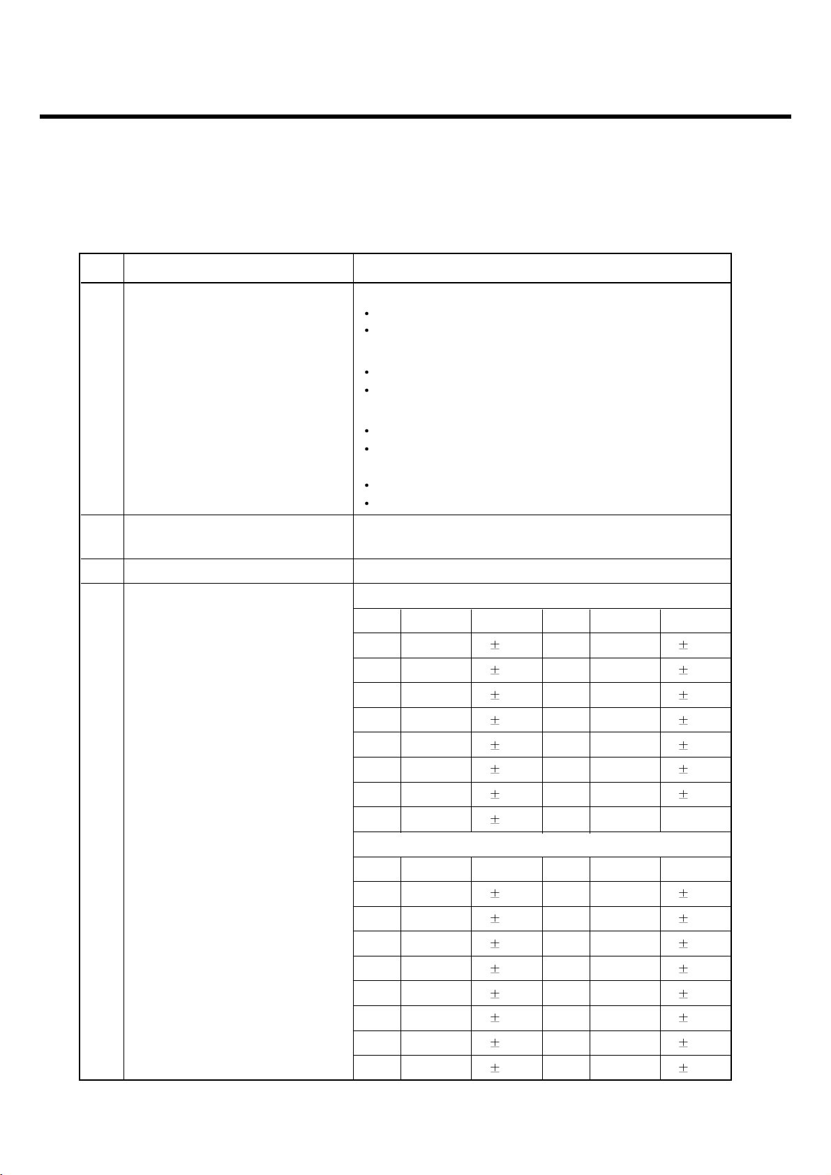
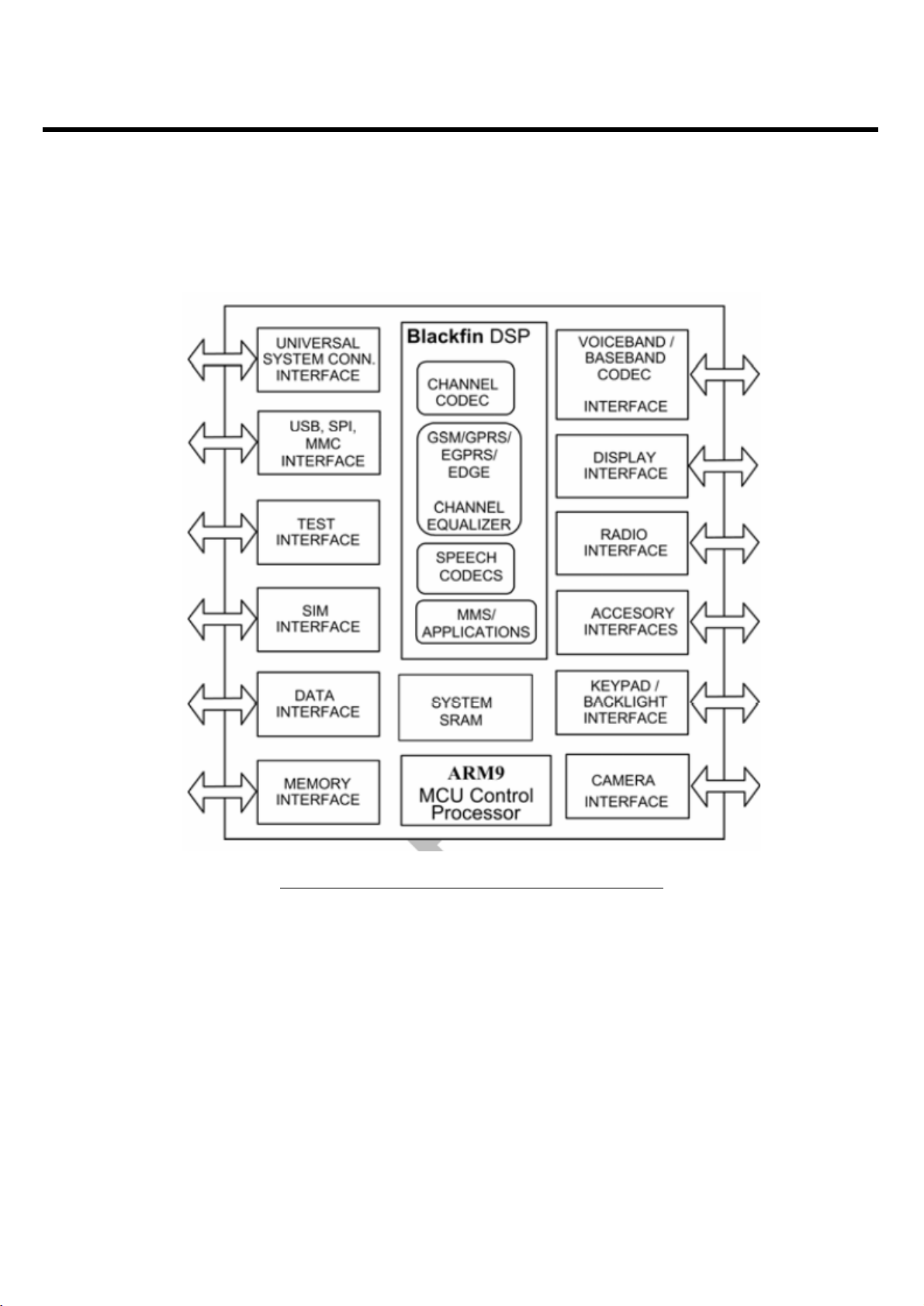
2. SYSTEM SPECIFICATION
2.1 H/W Features
2. SYSTEM SPECIFICATION
LGE Internal Use Only
Copyright © 2008 LG Electronics. Inc. All right reserved.
Only for training and service purposes
Item Feature Comment
Standard Battery Li-ion Polymer, 3.7V 800mAh
Stand by TIME Up to 200 hrs : Paging Period 5, RSSI 85dBm
Talk time Up to 200min : GSM Tx Level 7
Stand by time Up to 200 hours (Paging Period: 5, RSSI: -85 dBm)
Charging time Approx. 3 hours
RX Sensitivity GSM850/EGSM: -109dBm, DCS/PCS: -109dBm
TX output power
GSM850, EGSM: 32.4dBm(Level 5),
DCS , PCS: 29.5dBm(Level 0)
GPRS compatibility Class 10
SIM card type 3V Small
Display
MAIN : TFT 240 × 320 pixel 262K Color
SUB : TFT 128 × 160 pixel 262K Color
Hard icons. Key Pad
Status Indicator
0 ~ 9, #, *, Up/Down/Left/Right/Ok Navigation Key
Menu Key, Clear Key, Back Key, Confirm Key
Send Key, Volume Key, PWR Key, Camera Key, Hot Key
ANT Internal
EAR Phone Jack Yes
PC Synchronization Yes
Speech coding EFR/FR/HR
Data and Fax Yes
Vibrator Yes
Loud Speaker Yes
Voice Recoding Yes
Microphone Yes
Speaker/Receiver 16Ø Speaker / 11x07 Receiver
Travel Adapter Yes
MIDI SW MIDI (Mono SPK)
Camera 2M
Bluetooth / FM Radio Bluetooth version 2.0 / 76~108MHz supported
Page 9
- 10 -
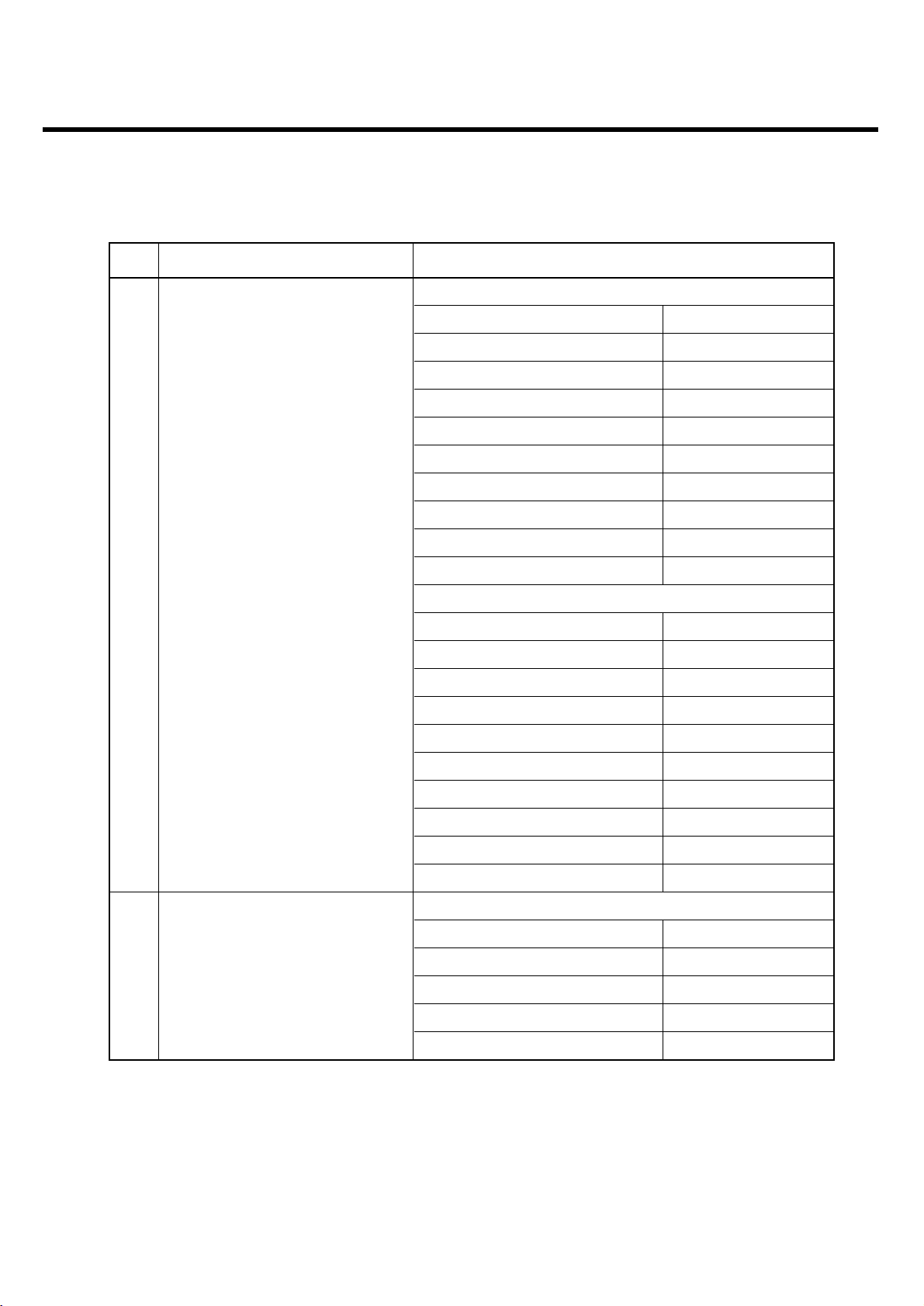
2. SYSTEM SPECIFICATION
2.2 Technical Specification
LGE Internal Use Only
Copyright © 2008 LG Electronics. Inc. All right reserved.
Only for training and service purposes
Item Description Specification
GSM850
TX: 824 ~ 849MHz
RX: 869 ~ 894MHz
EGSM
TX: 880 ~ 915MHz
RX: 925 ~ 960MHz
DCS1800
1Frequency Band TX: 1710 ~ 1785MHz
RX: 1805 ~ 1880MHz
PCS1900
TX: 1850 ~ 1910MHz
RX: 1930 ~ 1990MHz
2 Phase Error
RMS < 5 degrees
Peak < 20 degrees
3 Frequency Error < 0.1 ppm
GSM850/EGSM
Level Power Toler. Level Power Toler.
5 33 dBm 2dB 13 17 dBm 3dB
6 31 dBm 3dB 14 15 dBm 3dB
7 29 dBm 3dB 15 13 dBm 3dB
8 27 dBm 3dB 16 11 dBm 5dB
9 25 dBm 3dB 17 9 dBm 5dB
10 23 dBm 3dB 18 7 dBm 5dB
11 21 dBm 3dB 19 5 dBm 5dB
4 Power Level 12 19 dBm 3dB
DCS/PCS
Level Power Toler. Level Power Toler.
0 30 dBm 2dB 8 14 dBm 3dB
1 28 dBm 3dB 9 12 dBm 4dB
2 26 dBm 3dB 10 10 dBm 4dB
3 24 dBm 3dB 11 8 dBm 4dB
4 22 dBm 3dB 12 6 dBm 4dB
5 20 dBm 3dB 13 4 dBm 4dB
6 18 dBm 3dB 14 2 dBm 5dB
7 16 dBm 3dB 15 0 dBm 5dB
Page 10
- 11 -
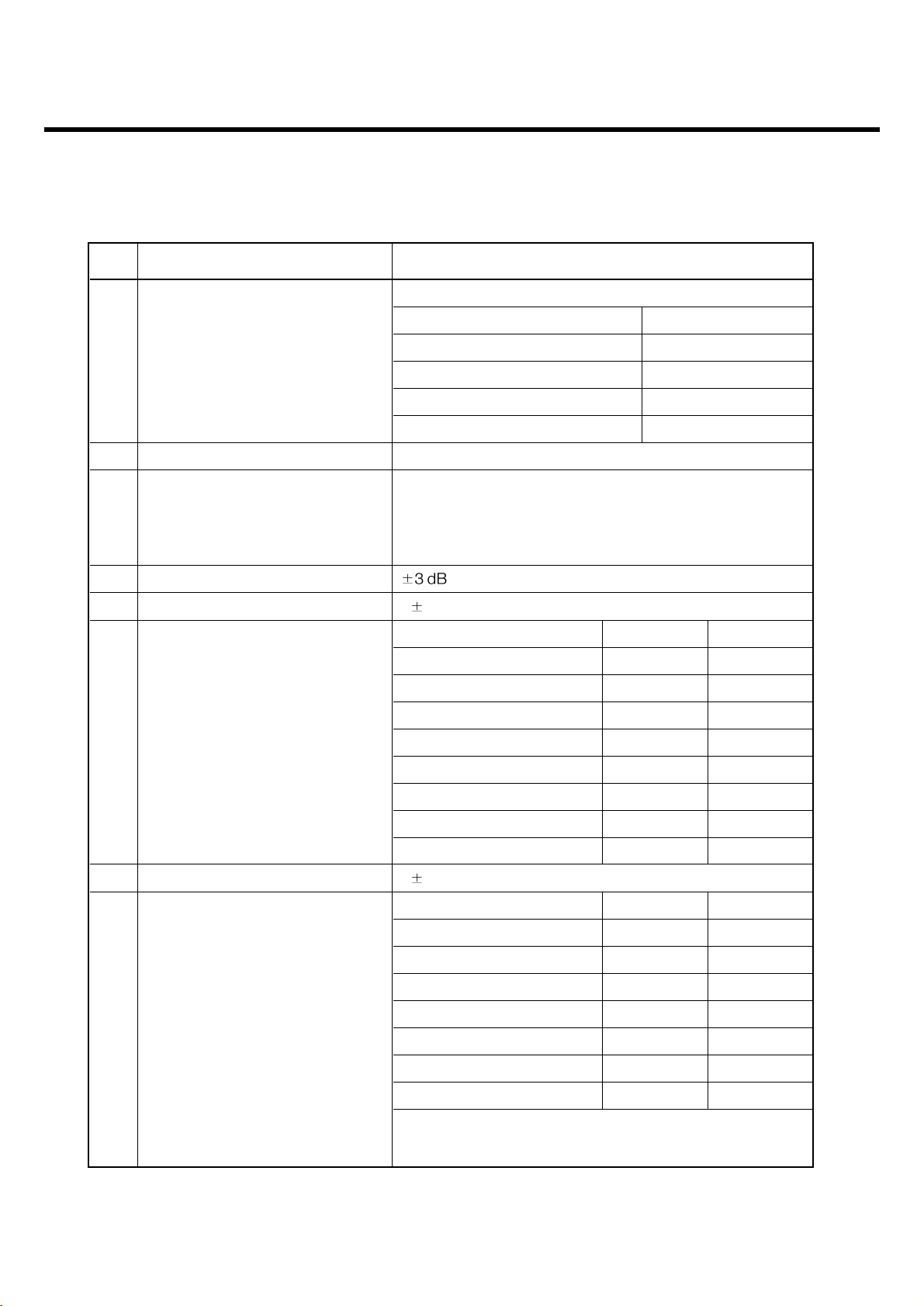
2. SYSTEM SPECIFICATION
LGE Internal Use Only
Copyright © 2008 LG Electronics. Inc. All right reserved.
Only for training and service purposes
Item Description Specification
GSM850/EGSM
Offset from Carrier (kHz). Max. [dBc]
100 0.5
200 -30
250 -33
400 -60
600 ~ 1,200 -60
1,200 ~ 1,800 -60
1,800 ~ 3,000 -63
3,000 ~ 6,000 -65
5
Output RF Spectrum 6,000 -71
(due to modulation) DCS/PCS
Offset from Carrier (kHz). Max. [dBc]
100 0.5
200 -30
250 -33
400 -60
600 ~ 1,200 -60
1,200 ~ 1,800 -60
1,800 ~ 3,000 -65
3,000 ~ 6,000 -65
6,000 -73
GSM850/EGSM
Offset from Carrier (kHz) Max. [dBm]
Output RF Spectrum 400 -19
6
(due to switching transient) 600 -21
1,200 -21
1,800 -24
Page 11
- 12 -
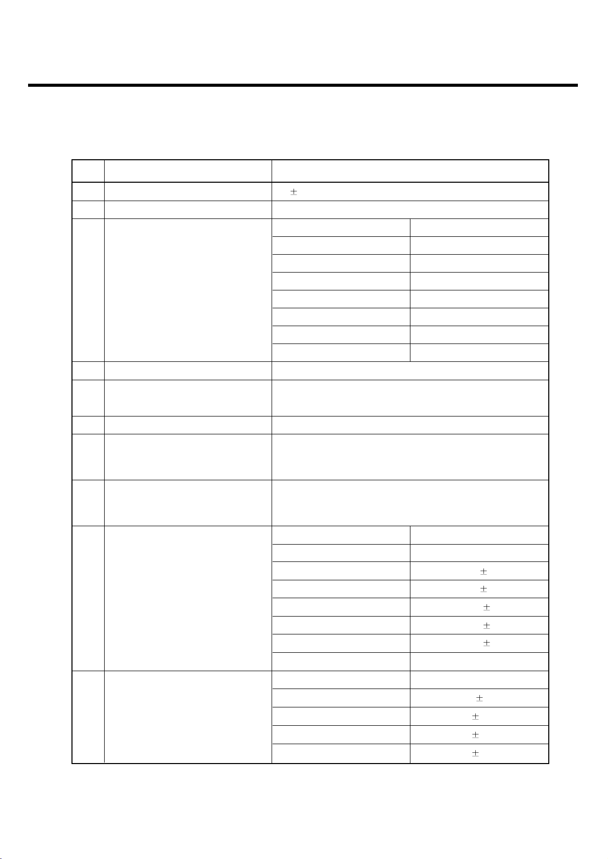
2. SYSTEM SPECIFICATION
LGE Internal Use Only
Copyright © 2008 LG Electronics. Inc. All right reserved.
Only for training and service purposes
Item Description Specification
DCS/PCS
Offset from Carrier (kHz) Max. [dBm]
Output RF Spectrum 400 -22
6
(due to switching transient) 600 -24
1,200 -24
1,800 -27
7 Spurious Emissions Conduction, Emission Status
GSM850/EGSM
8Bit Error Ratio
BER (Class II) < 2.439% @-102 dBm
DCS/PCS
BER (Class II) < 2.439% @-100 dBm
9 RX Level Report Accuracy
10 SLR 8 3 dB
Frequency (Hz) Max.(dB) Min.(dB)
100 -12 -
200 0 -
300 0 -12
11 Sending Response 1,000 0 -6
2,000 4 -6
3,000 4 -6
3,400 4 -9
4,000 0 -
12 RLR 2 3 dB
Frequency (Hz) Max.(dB) Min.(dB)
100 -12 -
200 0 -
300 0 -12
13 Receiving Response
1,000 0 -6
3,000 4 -6
3,400 4 -6
4,000 4 -9
*Mean that Adopt a straight line in between 300 Hz
and 1,000 Hz to be Max. level in the range.
Page 12
- 13 -
2. SYSTEM SPECIFICATION
LGE Internal Use Only
Copyright © 2008 LG Electronics. Inc. All right reserved.
Only for training and service purposes
Item Description Specification
14 STMR 13 5 dB
15 Stability Margin > 6 dB
dB to ARL (dB) Level Ratio (dB)
-35 17.5
-30 22.5
16 Distortion
-20 30.7
-10 33.3
0 33.7
7 31.7
10 25.5
17 Side Tone Distortion Three stage distortion < 10%
18
System frequency
≤2.5 ppm
(13 MHz) tolerance
19 32.768KHz tolerance ≤ 30 ppm
At least 65 dBspl under below conditions:
20 Ringer Volume 1. Ringer set as ringer.
2. Test distance set as 50 cm
Fast Charge : Typ. 430 mA
21 Charge Current Slow Charge : Typ. 80mA
Total Charging Time : < 3 hours
Bar Number Power
7 -93~
7 → 5 -93 2
22 Antenna Display 5 → 4 -98 2
4 → 2-101 2
2 → 1-104 2
1 → 0-106 2
0 → OFF ~-106
Battery Bar Number Voltage
3≤3.75 0.05 V
23 Battery Indicator 3 → 2 3.75 0.05 V
2 → 1 3.64 0.05 V
1 → 0 3.54 0.05 V
Page 13
Item Description Specification
24
Low Voltage Warning ≤ 3.54 0.05V (Call)
(Blinking Bar) ≤ 3.4 0.05V (Standby)
25
Forced shut down
3.33 0.05V
Voltage
26 Sustain RTCwithout battery Over 50 hours
Li-Ion Battery
27 Battery Type
Standard Voltage = 3.7 V
Battery full charge voltage = 4.2 V
Capacity: 800mAh
Switching-mode charger
28 Travel Charger Input: 100 ~ 350V, 50/60 Hz
Output: 5.1 V, 700 mA
- 14 -
2. SYSTEM SPECIFICATION
LGE Internal Use Only
Copyright © 2008 LG Electronics. Inc. All right reserved.
Only for training and service purposes
Page 14
- 15 -
3. TECHNICAL BRIEF
3. TECHNICAL BRIEF
LGE Internal Use Only
Copyright © 2008 LG Electronics. Inc. All right reserved.
Only for training and service purposes
3.1 Digital Main Processor(AD6900, U101)
The AD6900 is an advanced, low-power baseband processing solution from Analog Devices, and is
part of the AD20msp500 SoftFone® chipset family. The AD6900 is intended for use in a wide variety of
feature-rich phones with GSM/GPRS/EGPRS based system connectivity requirements. It is designed
to interface easily to an application/OS processor, or to stand alone as a fully integrated and easy-touse solution for mobile handset and wireless modem applications.
Figure. 3-1 AD6900 FUNCTIONAL BLOCK DIAGRAM
Page 15
- 16 -
3. TECHNICAL BRIEF
LGE Internal Use Only
Copyright © 2008 LG Electronics. Inc. All right reserved.
Only for training and service purposes
3.1.1 Features of AD6900
Complete Single-Chip Programmable Digital Baseband Processor with four main subsystems
MCU Control Processor Subsystem:
32-bit ARM926EJ-S® MCU Control Processor
260 MHz operation at 1.5V
dedicated caches, 16K bytes each, for instructions and data
4kB Instruction Tightly Coupled Memory (TCM)
2-Mbit On-chip System SRAM
Ciphering coprocessor for GPRS supporting GEA1 and GEA2 encryption algorithms
Kasumi cipher coprocessor for GEA3 encryption
Dedicated multichannel DMA controller
DSP Subsystem:
Blackfin 16-bit fixed-point DSP Processor
260 MHz operation at 1.5V
Memory:
→ L1 program space: 64 kB SRAM and 16 kB configurable as instruction cache or SRAM
→ L1 data space: Two banks of 16K bytes, each with 8K bytes of dedicated SRAM and an
additional 8K bytes that can be configured as either cache or SRAM
→ L2 space: 64KB SRAM
Ciphering coprocessor (GEA1 and GEA2)
Kasumi cipher coprocessor for GEA3 encryption
Dedicated multichannel DMA controller
Peripherals Subsystem:
Shared on-chip peripherals and off-chip interfaces:
Support for Burst-mode, Page-mode, and NAND Flash memory
Support for SRAM, SDRAM, and PSRAM (cellular RAM)
Full-Speed USB 2.0 Dual-Role Interface with OTG (On-The-Go) Host Mode or traditional Peripheralonly mode
Page 16

- 17 -
3. TECHNICAL BRIEF
LGE Internal Use Only
Copyright © 2008 LG Electronics. Inc. All right reserved.
Only for training and service purposes
Applications Subsystem for Enhanced Multimedia:
Parallel Peripheral Interface (PPI) for 10-bit dedicated camera
sensor or video input interface (including ITU-656 and ITU-601 digital video)
Separate external bus interface for parallel LCD displays (or camera module inputs)
- reduces noise and loading on the
main EBUS interface
Dedicated multi-channel DMA controller
OTHER FEATURES
Real-Time Clock (RTC) with Alarm
Four General-Purpose Timers
Baseband Converter Interface
Compatible with Othello® radio subsystem
Highly configurable interrupt controller architecture
Programmable bus arbitration to optimize system performance
Supports 13 MHz and 26 MHz Input Clocks
Programmable Power Management and Clock Management
- Slow Clocking Scheme for Low Idle Mode Current
- Power Down modes
- Dynamic Core Voltage Scaling from 1.1 - 1.5V
Independent I/O Voltage Domains
On-chip support for EGPRS Data Services up to Class 10
Embedded Trace Macrocell for MCU Debug
JTAG Interface for Test and In-Circuit Emulation of both the MCU and DSP Advanced features for
security
Page 17
LGE Internal Use Only
Copyright © 2008 LG Electronics. Inc. All right reserved.
Only for training and service purposes
3. TECHNICAL BRIEF
- 18 -
3.2 Analog Main Processor(AD6855, U100)
The AD6855 is a complete mixed-signal baseband processor that combines all of the data converters
and power supply regulators required for a GSM 900 / GSM 850 / DCS 1800 / PCS 1900 mobile on a
single device, including HSCSD, GPRS and EGPRS.
Figure. 3-2-1 AD6855 FUNCTIONAL BLOCK DIAGRAM
Page 18

- 19 -
3. TECHNICAL BRIEF
LGE Internal Use Only
Copyright © 2008 LG Electronics. Inc. All right reserved.
Only for training and service purposes
3.2.1 General Description
The AD6855 baseband transmit section supports the following mobile station GMSK modulation power
classes:
GSM 900/850 power classes 4 and 5,
DCS 1800 power classes 1 and 2, and
PCS 1900 power classes 1 and 2.
The AD6855 baseband transmit section supports the following mobile station 8-PSK modulation power
classes:
GSM 900/850 power classes E2 and E3,
DCS 1800 power classes E2 and E3, and
PCS 1900 power classes E2 and E3.
The AD6855 baseband receive section supports GMSK and 8-PSK applications.
The AD6855 auxiliary section provides a voltage reference, an automatic frequency control DAC, an
auxiliary ADC, and light controllers. The auxiliary ADC provides two channels for measuring
temperature using discrete external devices placed in critical locations. The AD6855 audio section
provides 8 kHz and 16 kHz sampling rates for voiceband data input and output and provides nine
standard sample rates ranging from 8kHz to 48 kHz for personal audio output on two PCM Audio serial
ports. The two Audio serial ports allow support for concurrency. The AD6855 power management
section provides voltage regulators for digital and analog components, a battery charger, battery
protection circuitry, and power supply activation logic. The AD6855 digital processor interface provides
serial ports for control data, baseband transmit and receive data, and two for audio data.
Page 19
- 20 -
3. TECHNICAL BRIEF
LGE Internal Use Only
Copyright © 2008 LG Electronics. Inc. All right reserved.
Only for training and service purposes
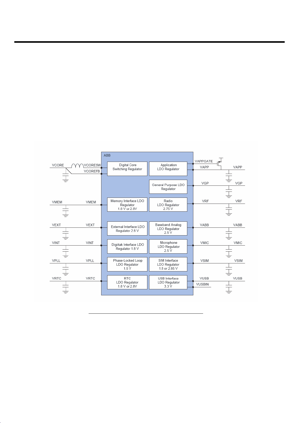
3.2.2 Power Block
CSPORT interface, power management control interface and the circuit that generates power up
RESET pulses (RESET2P8 and RESET1P8) for use by the DBB chip.
All regulators except the USB interface regulator are powered from the main battery.
The USB regulator is powered from USB VBUS.
And the user presses KEYON which puts the AD6855 power management system into ACTIVATION
state (see definitions below) and signals DBB software that it’s time to wake up and operate using the
KEYOUT signal.
Figure. 3-2-2 AD6855 POWER BLOCK DIAGRAM
Page 20
- 21 -
3. TECHNICAL BRIEF
LGE Internal Use Only
Copyright © 2008 LG Electronics. Inc. All right reserved.
Only for training and service purposes
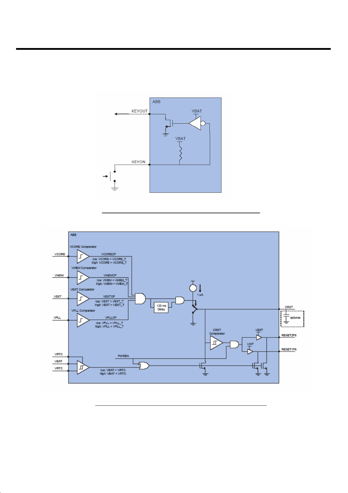
Figure. 3-2-3 AD6855 KEYON/KEYOUT BLOCK DIAGRAM
Figure. 3-2-4 AD6855 RESET GENERATION BLOCK DIAGRAM
Page 21

- 22 -
3. TECHNICAL BRIEF
LGE Internal Use Only
Copyright © 2008 LG Electronics. Inc. All right reserved.
Only for training and service purposes
Power On Reset Generator
The power-on reset signals (RESET1P8 and RESET2P8) are asserted based on the VCORE (if
VAPPCFG = 0), VMEM, VEXT, and VPLL regulators. RESET1P8 and RESET2P8 are low when reset
is enabled and high when reset is disabled.
When the outputs of all four regulators reach their corresponding threshold voltages, reset will be
disabled after a nominal reset period of 130ms.
The outputs of all four regulators must remain at or above their corresponding threshold voltages for
the duration of the reset period for reset to be disabled (pulled high).
The nominal 130ms reset period is restarted whenever all four regulators reach their threshold
voltages. The nominal reset period of 130ms can be extended by connecting an external capacitor to
CRST. This capacitor is charged using a small current when reset is enabled. Once the capacitor
reaches the threshold, reset is disabled.
Reset will be enabled immediately if any one of the four regulators falls below their corresponding
threshold voltages. In addition, reset will be enabled if VBAT falls below VRTC. The PWREN signal is
the logical AND of all the state controls that enable or disable many of the regulators on the chip. If the
regulators enabled by PWREN are disabled by PMT state controls described below then PWREN
must go low.
When PWREN goes low reset will be immediately enabled causing RESET1P8 and RESET2P8 to be
pulled low.
When reset is enabled, both RESET1P8 and RESET2P8 are actively pulled low. CRST is also actively
pulled low when reset is enabled.
VABB Regulator Enable/Disable Logic Operation
The VABB regulator powers many on-chip analog circuits on the ABB. The VCXOEN signal, the
VABBEn bit in the LDOControl1 Bit Positions ( Addr 0x35) register, and the AFCDACMode and
AFCDACOn bits in the AuxControl1 Bit Positions ( Addr 0x13) register all particpate in controlling the
VABB enable/disable.
When the ABB power management system transitions from Off state, DDLO state, UVLO state, or
Thermal Shutdown State to Power Key Activation, Charger Activation, USB Charger Activation, or
Active State VABB will be enabled. During these state transitions ABBEn = 0 and AFCDACMode = 0,
VRF is enabled.
Once the ABB power management system is in Power Key Activation, Charger Activation, USB
Charger Activation, Active-Standby or Active State the VABB regulator enable/disable is controlled by
the information written to the VABBEn and AFCDACMode register bits by system software.
Page 22

- 23 -
3. TECHNICAL BRIEF
LGE Internal Use Only
Copyright © 2008 LG Electronics. Inc. All right reserved.
Only for training and service purposes
Digital Baseband Core (VCORE)
The Digital Baseband Core regulator supplies the digital baseband processor (DBB) core.
The voltage on VCORE is selectable using the VCOREControl register.
The VCOREActive code selects the voltage on VCORE in high power mode and the VCOREStandby
code selects the voltage on VCORE in low-power mode.
DBB Interface (VINT)
The DBB interface regulator supplies the DBB/ABB digital interfaces. The output voltage of the VINT
regulator is nominal 1.8V.
Memory (VMEM)
The VMEM regulator supplies the external memory(s) and the interface to the external memory on the
digital baseband processor. The output voltage of the Memory Interface regulator can be selected as
1.8V nominal or 2.8V nominal using the VMEMSEL terminal.
External Interface (VEXT)
The External Interface regulator supplies the Radio digital interface and the high voltage (>1.8V)
interface between the digital baseband processor and various peripherals, such as the LED indicators
and the LCD display.
SIM Interface (VSIM)
AD6855 is designed to support 3.0 V and 1.8 V SIMs exclusively (i.e. no 5 V SIMs).
The SIM Interface regulator supplies the SIM interface circuitry on the digital processor and the SIM
card. By default the SIM Interface regulator output is 2.85 V, which can be decreased to 1.8 V if a 1.8
V SIM is detected.
Real-Time Clock (VRTC)
The Real-Time Clock regulator supplies the Real-Time Clock module. The Real-Time Clock regulator
is optimized for low ground current.
Baseband Analog (VABB)
The Baseband Analog regulator supplies the analog portions of the AD6855. Operation of the VABB
regulator is controlled by the VABBEn bit in the LDOControl1 register.
If VABBEn = 0, the VABB regultor will be disabled unless the AFCDAC is enabled or VCXOEN = 1. If
VABBEn = 1 (the default state) VABB is enabled along with VCORE, VMEM, and VEXT. The
Baseband Analog regulator is optimized for high ripple rejection and low noise. The output of the
Baseband Analog regulator should not be used as a supply for any external components.
Page 23

- 24 -
3. TECHNICAL BRIEF
LGE Internal Use Only
Copyright © 2008 LG Electronics. Inc. All right reserved.
Only for training and service purposes
Microphone (VMIC)
The Microphone regulator supplies the microphone interface circuitry. The Microphone regulator is
optimized for extremely high ripple rejection up to 217 Hz and low noise.
VRF (VRF)
The VCXO regulator supplies the voltage controlled crystal oscillator (VCXO). The VCXO regulator is
optimized for high ripple rejection and low noise.
USB Interface (VUSB)
The VUSB regulator supplies the USB transceiver located in the DBB. Digital Baseband PLL (VPLL)
The VPLL regulator supplies the phase locked loop on the digital baseband (DBB).
General Purpose Regulator (VGP)
The General Purpose regulator is intended primarily to serve as a supply rail for camera modules. Its
voltage is programmable by setting VGPSel[3:0] in theLDOControl2 Register. VGP is enabled by
setting the VGPEn bit in LDOControl1 to 1.
Applications Regulator (VAPP)
The VAPP regulator is an adjustable regulator that uses an off chip pass device. It has two modes of
operation selected by the state of the VAPPCFG terminal. If VAPPCFG is pulled low the VAPP
regulator functions as a programmable voltage applications supply.
In this mode, VAPP is enabled or disabled using the VAPPEn bit of LDOControl1.
Page 24
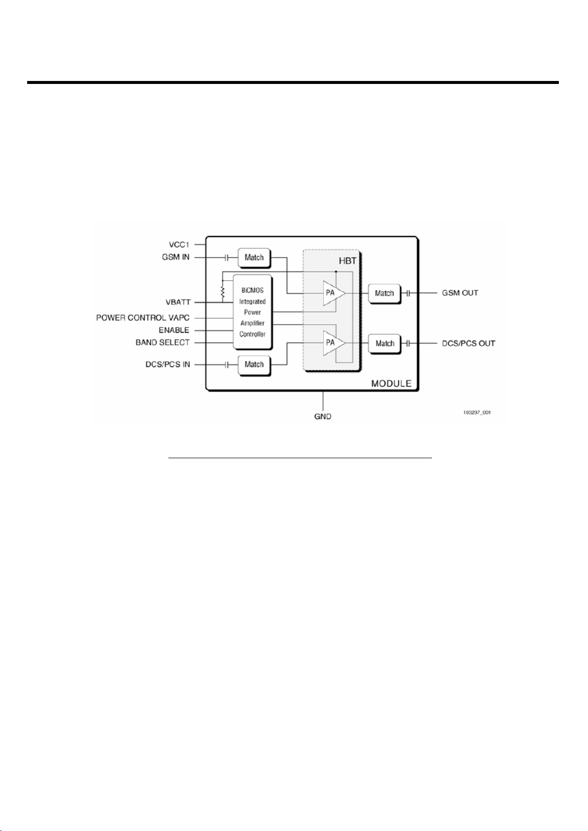
3.3 Power Amplifier Module(SKY77318, U601)
3.3.1 Internal Block Diagram
3.3.2 General Description
The SKY77318 Power Amplifier Module (PAM) is designed in a low profile (1.2 mm), compact form
factor for quad-band cellular handsets comprising GSM850/900, DCS1800, and PCS1900 operation.
The PAM also supports Class 12 General Packet Radio Service (GPRS) multi-slot operation.
The module consists of separate GSM PA and DCS1800/PCS1900 PA blocks, impedance-matching
circuitry for 50 ߟ input and output impedances and a Power Amplifier Control (PAC) block with an
internal current-sense resistor. The custom BiCMOS integrated circuit provides the internal PAC
function and interface circuitry.
Fabricated onto a single Gallium Arsenide (GaAs) die, one Hetero-junction Bipolar Transistor (HBT)
PA block supports the GSM bands and the other supports the DCS1800 and PCS1900 bands. Both
PA blocks share common power supply pins to distribute current.
- 25 -
3. TECHNICAL BRIEF
LGE Internal Use Only
Copyright © 2008 LG Electronics. Inc. All right reserved.
Only for training and service purposes
Figure. 3-3-1 SKY77318 FUNCTIONAL BLOCK DIAGRAM
Page 25
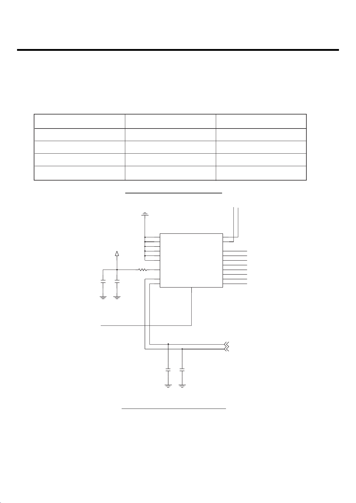
3.4 FEM (DGM1110M014, FL601)
The FEM is integrated of quadband RX SAWs, internal diplexer and ESD protection at Ant port to 8kV
acc.
- 26 -
3. TECHNICAL BRIEF
LGE Internal Use Only
Copyright © 2008 LG Electronics. Inc. All right reserved.
Only for training and service purposes
Figure 3-4-2 FEM CIRCUIT DIAGRAM
Figure 3-4-1 Band SW Logic Table
2
1
ANT_SW1 ANT_SW2
GSM850/900 TX L H
DCS/PCS TX H H
GSM850/900 RX L L
DCS/PCS RX H L
GND6
20
2V75_VCXO
C632
39p
C628
0.1u
R612
10
GND5
19
GND4
18
GND3
16
GND2
11
GND1
9
VDD
12
VC2
13
VC1
14
DGM1110M014
C643
FL601
100p
GSM1800_1900_TX
C644
100p
GSM850_900_TX
GSM1900_RX2
GSM1900_RX1
GSM1800_RX2
GSM1800_RX1
GSM900_RX2
GSM900_RX1
GSM850_RX2
ANT
GSM850_RX1
17
15
10
8
7
6
5
4
3
2
1
ANT_SW
ANT_SW
Page 26
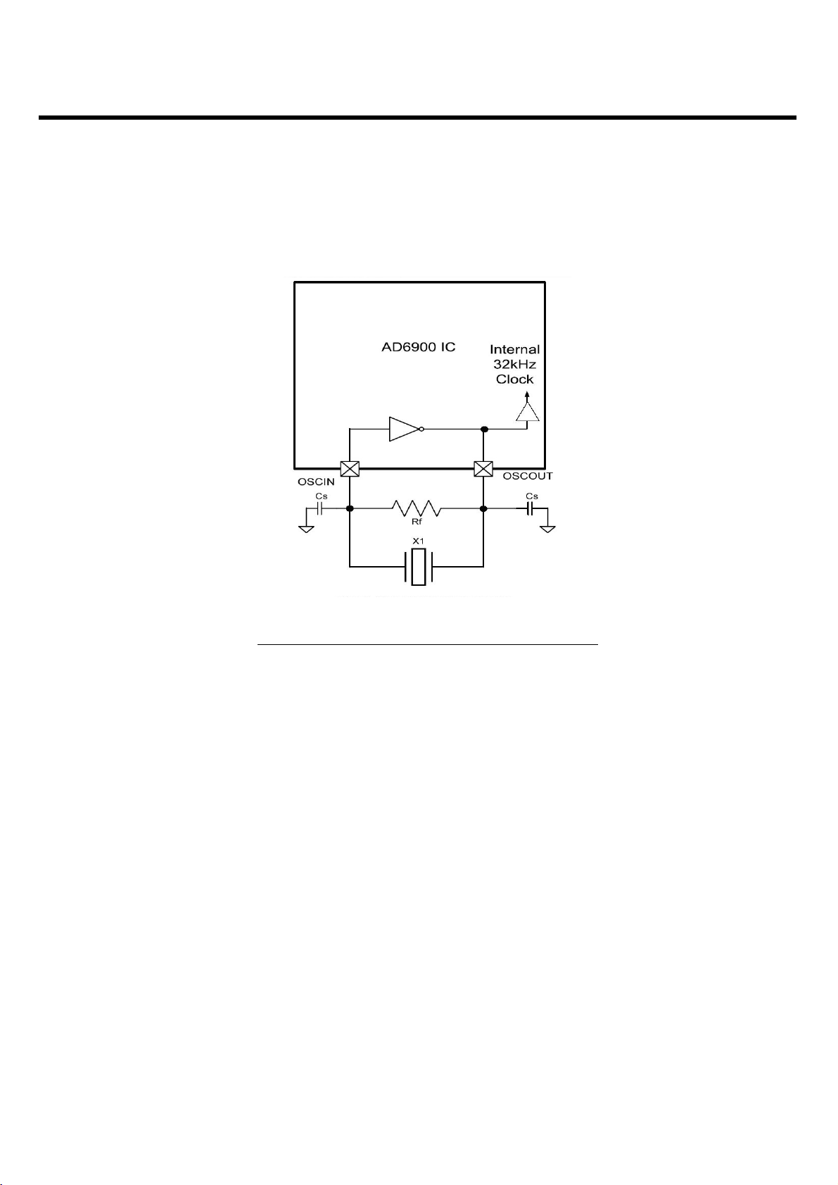
3.5 RTC(FC-135, X100)
The AD6900 supports a Real Time Clock function. A total of 25pF+/-10% capacitance to graound is
required (including board trace capacitance) on each OSCIN and OSCOUT.
RTC functionality allows the application software to implement standard clock, calendar, or organizer
functions.
A 32KHz clock is required in AD6900 based systems to take advantage of power saving “slow
clocking” mode. A combination of an oscillator circuit within the AD6900 IC and an external 32KHz
crystal results in a stable 32kHz clock for use in the system. The purpose of this application note is to
discuss the system issues that affect operation of the 32kHz oscillator circuit.
- 27 -
3. TECHNICAL BRIEF
LGE Internal Use Only
Copyright © 2008 LG Electronics. Inc. All right reserved.
Only for training and service purposes
Figure. 3-5-1 32.768KHz Crystal Basic Connections
Page 27
- 28 -
3. TECHNICAL BRIEF
LGE Internal Use Only
Copyright © 2008 LG Electronics. Inc. All right reserved.
Only for training and service purposes
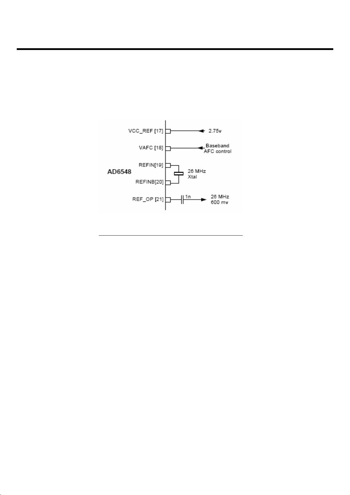
3.6 Crystal(26 MHz, X601)
The AD6548 requires only an external low cost as the frequency reference. The circuitry to oscillate
the crystal and tune its frequency is fully integrated. The Oscillator is a balanced implementation
requiring the crystal to be connected across 2 pins. There is a programmable capacitor array
included for coarse tuning of fixed offsets, and an integrated varactor for dynamic control. The
oscillator is designed for use with a 26MHz crystal. The crystal is connected as shown in figure 3-3.
Figure. 3-6-1 Crystal Oscillator External Connection
Page 28
- 29 -
3. TECHNICAL BRIEF
LGE Internal Use Only
Copyright © 2008 LG Electronics. Inc. All right reserved.
Only for training and service purposes
Dedicated control software ensures excellent frequency stability under all circumstances. The AD6548
reference oscillators provides a 26MHz 600mVpp (typical) output (REF_OP), for use as the baseband
clock input.
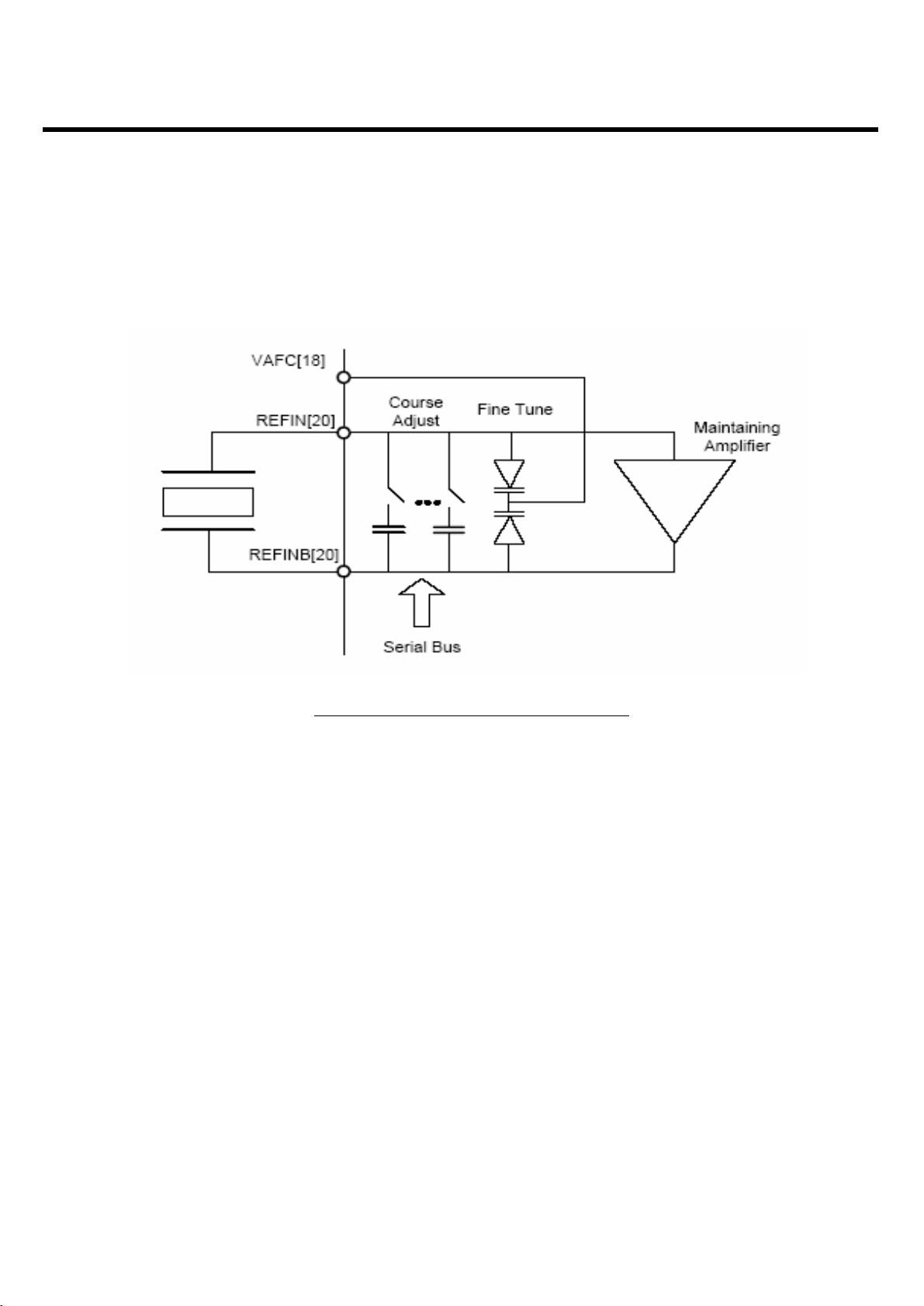
The AD6548 integrates this frequency tuning range the tuning section comprises a switchable
capacitor array for discrete steps and varactor for fine tuning. Contol of the tuning process is driven by
software, whereby the frequency can be maintained accurately during reception gaps and initial
frequency upon startup can be accurately estimated without the need for temperature sensors.
Figure. 3-6-2 Crystal Circuit Block Diagram
Page 29
- 30 -
3. TECHNICAL BRIEF
LGE Internal Use Only
Copyright © 2008 LG Electronics. Inc. All right reserved.
Only for training and service purposes
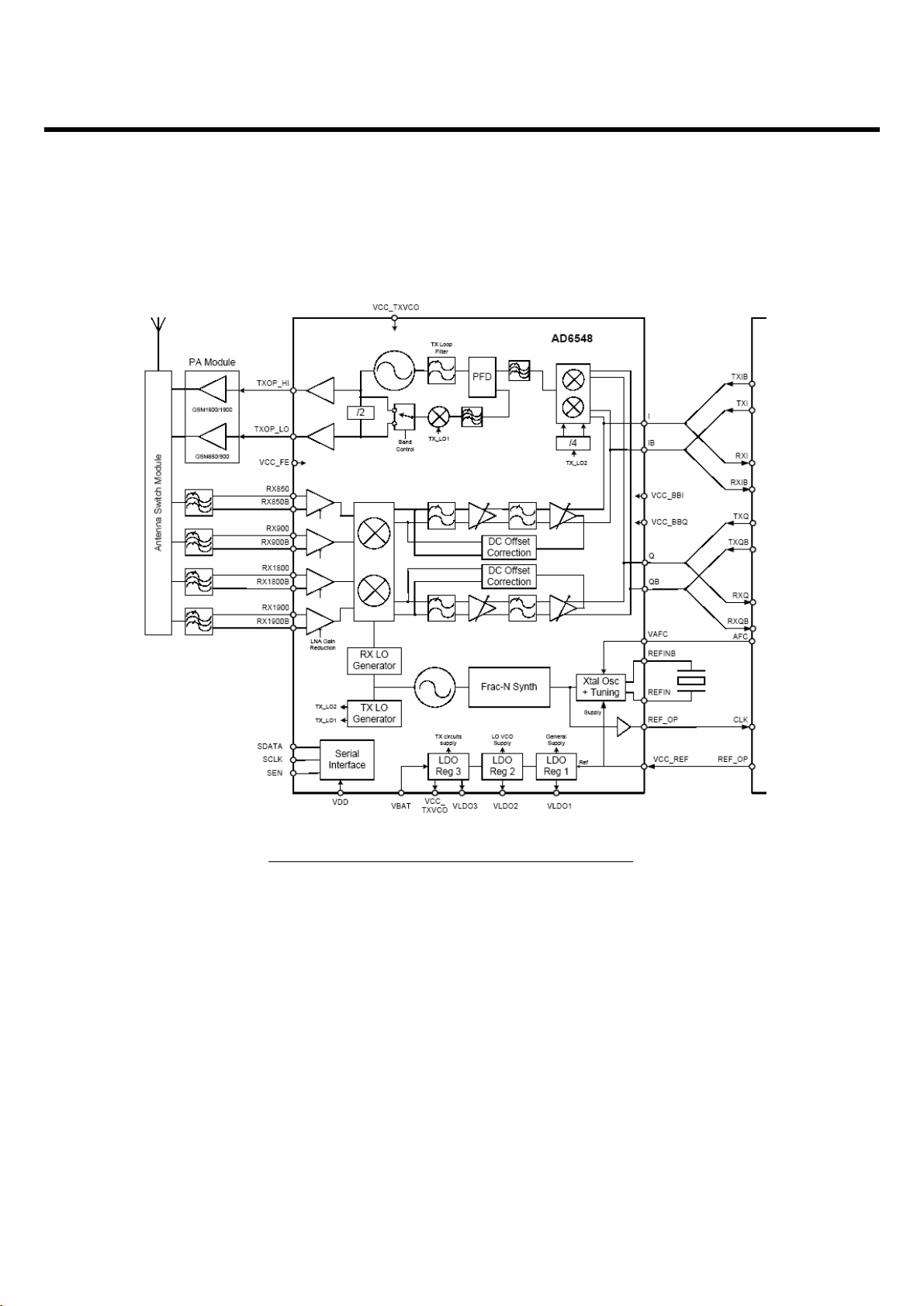
3.7 RF Tranceiver(AD6548, U602)
3.7.1 GENERAL DESCRIPTION
The AD6548 provides a highly integrated direct conversion radio solution that combines, on a single
chip, all radio and power management functions necessary to build the most compact GSM radio
solution possible. The only external components required for a complete radio design are the Rx
SAWs, PA, Switchplexer and a few passives enabling an extremely small cost effective GSM Radio
solution.
The AD6548 uses the industry proven direct conversion receiver architecture of the OthelloTM family.
For Quad band applications the front end features four fully integrated programmable gain differential
LNAs. The RF is then downconverted by quadrature mixers and then fed to the baseband
programmable-gain amplifiers and active filters for channel selection. The Receiver output pins can be
directly connected to the baseband analog processor. The Receive path features automatic calibration
and tracking to remove DC offsets.
Figure. 3-7-1 CIRCUIT DIAGRAM of RF Tranceiver
Page 30
- 31 -
3. TECHNICAL BRIEF
The transmitter features a translation-loop architecture for directly modulating baseband signals onto
the integrated TX VCO. The translation-loop modulator and TX VCO are extremely low noise removing
the need for external SAW filters prior to the PA.
The AD6548 uses a single integrated LO VCO for both the receive and the transmit circuits. The
synthesizer lock times are optimized for GPRS applications up to and including class 12.
3.7.2 FUNCTIONAL DESCRIPTION
LGE Internal Use Only
Copyright © 2008 LG Electronics. Inc. All right reserved.
Only for training and service purposes
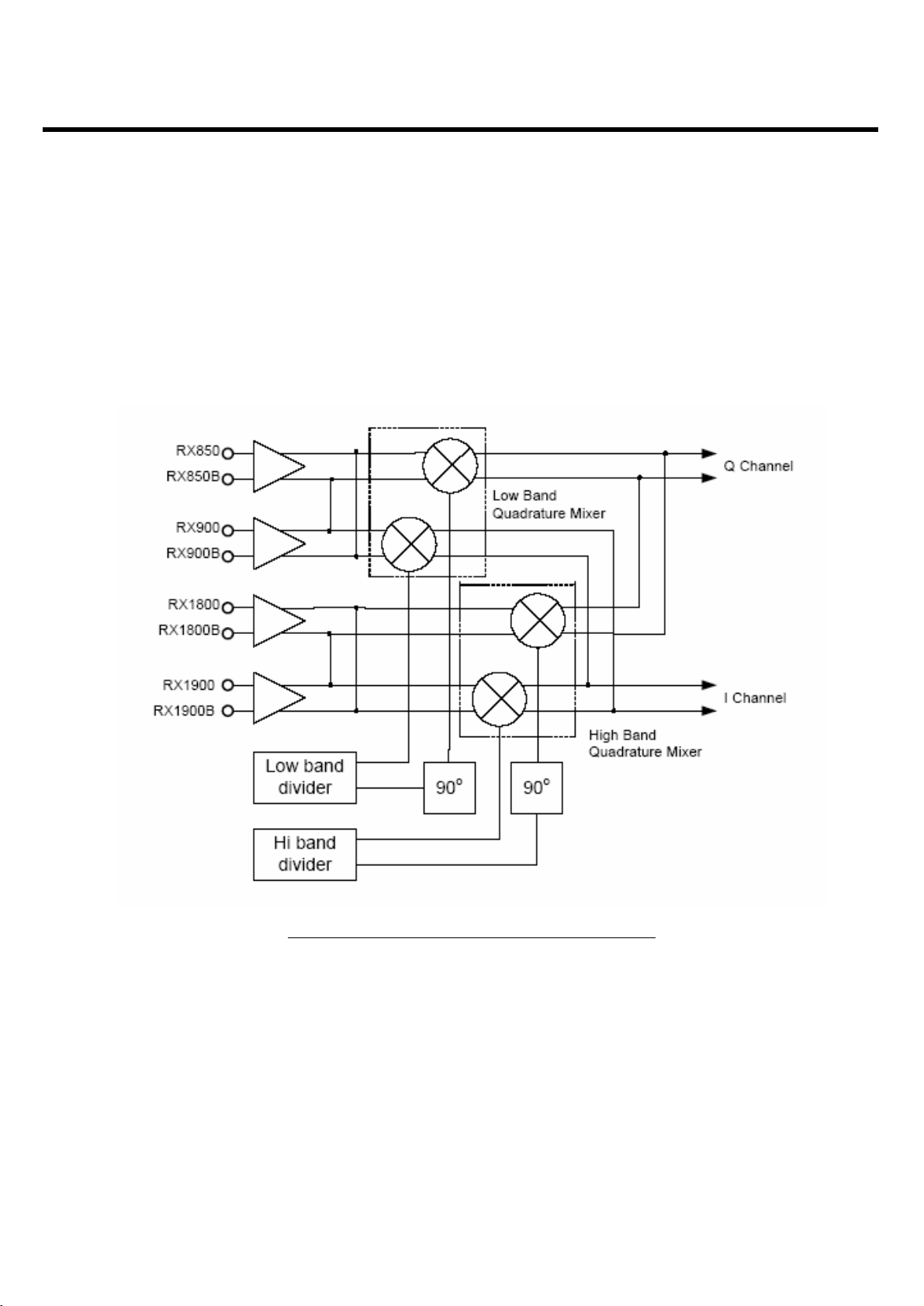
Figure. 3-7-2 RECEIVER CHAIN BLOCK DIAGRAM
Page 31

- 32 -
3. TECHNICAL BRIEF
LGE Internal Use Only
Copyright © 2008 LG Electronics. Inc. All right reserved.
Only for training and service purposes
3.7.2.1 RECEIVER CHAIN
The AD6548/9 receiver section fully integrates all the RF and baseband signal processing. Each major
block is described in the following sections.
Low Noise Amplifiers
The AD6548 includes four fully integrated Low Noise Amplifiers (LNAs), to support quad band
applications without further external active components. The LNAs have differential inputs which
minimize the effect of unwanted interferers. The inputs are easily matched to industry standard
Front End Modules (FEMs) or discrete Rx SAW filters. The outputs of the LNAs are directly coupled
to the down-converting mixers.
The voltage gain of the LNAs are typically 24 dB. Each LNA can be switch to a low gain mode when
receiving large input signals as part of the AGC system.
Down-Converting Mixers Two quadrature mixers are used to mix down the signals from the LNAs,
one for the high bands (1800 and 1900 MHz) and one for the low bands (850 and 900 MHz). The
outputs of the mixers are connected to the baseband section through an integrated single pole filter
with nominal cut-off frequency of 800kHz. This acts as a “roofing filter” for the largest blocking
signals (i.e. those ≥ 3MHz) and prevents the baseband amplifiers from being overloaded.
Baseband Amplifiers / Low Pass Filters
The baseband amplifiers provide the majority of the analog receiver gain. The filtering is provided by
an integrated 5thorder Chebyshev filter giving the necessary adjacent channel and blocking filtering,
it is also acting as an anti-alias filtering for Baseband IC’s converters. A final low pass pole is
possible Baseband Output D.C. Offset Correction In order to minimize D.C. offsets inherent in the
receiver and maximize dynamic range a D.C offset correction circuit is integrated. This correction is
triggered over the serial bus and then an offset tracking loop is enabled to minimize residual offsets
under all conditions. The tracking loop is fully hardware integrated, requiring no software
intervention.
Receiver Local Oscillator (LO) Generator
The Rx LO generator is used to avoid DC offset problems associated with LO leakage into the
receiver RF path. By operating the VCO at a frequency other than the desired receive frequencies,
any leakage of the VCO will fall out of band. The LO generator is used to convert the offset
synthesized VCO output to the on-frequency quadrature LO required by the chipset. The LO
generator is implemented as a regenerative frequency divider, performing a 2/3 multiplication of the
VCO output for the high band (DCS1800/PCS1900) and a 1/3 multiplication for low band (E-GSM
900/GSM850).
Page 32

LGE Internal Use Only
Copyright © 2008 LG Electronics. Inc. All right reserved.
Only for training and service purposes
3. TECHNICAL BRIEF
- 33 -
3.7.2.2 Transmit Path
Overview
The transmit section of the AD6548/9 radio implements a translation loop modulator.
This consists of a quadrature modulator, high speed phase-frequency detector (PFD) with charge
pump output, loop filter, TX VCO and a feedback down converting mixer. The VCO output (divided
by 2 for low band) is fed to the power amplifier with a portion internally fed back into the downconverting feedback mixer to close the feedback loop.
Quadrature Modulator
The Quadrature modulator takes the baseband I & Q signals and translates these into a GMSK
signal at the Transmit Intermediate Frequency (TX IF). After bandpass filtering and limiting the TX IF
signal is used as the reference input to the Phase Frequency Detector (PFD) of the transmit PLL.
Figure. 3-7-3 TRANSMIT PATH BLOCK DIAGRAM
Page 33

LGE Internal Use Only
Copyright © 2008 LG Electronics. Inc. All right reserved.
Only for training and service purposes
3. TECHNICAL BRIEF
- 34 -
Phase Frequency Detector (PFD)
The PFD ensures that the transmitted signal contains the required modulation and is accurately
locked to the desired GSM channel. The downconverted feedback signal from the TX VCO and the
Quadrature Modulator output are phase compared by the PFD.
The PFD charge pump generates a current pulse proportional to the difference in phase which is
applied to the loop filter.
Loop filter
To minimize complexity of the external PCB layout the TX loop filter is fully integrated into the IC. At
power up the filter is automatically calibrated as part of the baseband filter cal, eliminating process
tolerances. The calibration is fully integrated and requires no extra programming.
TX VCO
The Transmit Voltage Controlled Oscillator (TX VCO) and tank components are a fully integrated
subsystem. The subsystem includes PA drivers so the outputs are used to directly drive the external
PAs. The low noise oscillator design and internal filtering mean that external TX SAW filters are not
required. In Low band operation the TX VCO output is divided by two and filtered. The TX VCO is
automatically calibrated to ensure optimum performance over its operating frequency of 1648 to
1910 MHz.
Feedback Down-Converting Mixer
The feedback down converting mixer is used to translate the TX VCO output frequency to the TX IF.
An integrated band pass filter exists between the mixer and the PFD to filter the mixers unwanted
side band and higher order mixing products.
Page 34

- 35 -
3. TECHNICAL BRIEF
LGE Internal Use Only
Copyright © 2008 LG Electronics. Inc. All right reserved.
Only for training and service purposes
3.7.2.3 Main Frequency Synthesizer
The AD6548 has a single fast-locking fractional synthesizer used for VCO control in both receive and
transmit mode. The entire system including VCO, tank, fractional N dividers, sigma delta
compensation, charge pump and loop filters are fully integrated.
The only external component is the frequency reference. The synthesizer is controlled via the serial
interface. The VCO is fed into the respective dividers to generate the appropriate LO frequencies for
the RX and TX bands.
Fractional N Dividers
The fractional N divider allows the PLL system to have a smaller step size than theb comparison
frequency which is set by the external reference to 26 MHz. This feature allows all the GSM
frequency band rasters to be achieved, with fast lock times and good phase noise characteristics.
The divider section consists of a dual modulus 8/9 prescaler, integer M & A dividers, and fractional
N system based on sigma-delta modulation to generate the required fractional divide ratio. The
Denominator of the fractional divider can be set to 3 different values, (1040, 1170, 1235), depending
on the mode of operation. For example a denominator of 1040 with an input fraction F maintains an
average value of F/1040 allowing 25 kHz steps when operated at a reference of 26 MHz.
The Overall count value is thus:
8*M + A + Fraction
Where: M is 4 bits, but the MSB is set to 1. A is 3 Bits. Fraction is N/ Denominator.
The Denominator is set to one of 3 values: 1040, 1170, 1235. N is a 11 bit value.
Values for M, A and N are loaded from serial interface word, but the denominator is automatically
set according to the mode.
Refer to the Programming Procedures for more details.
Phase Frequency Detector/Charge Pump
A Phase Frequency Detector (PFD) is used for the PLL phase detector. The charge pump is
designed such that good matching of up and down currents is achieved over a wide output
operating range. The charge pump output is internally routed to the integrated synthesizer loop filter.
Synthesizer Loop filter
To minimize complexity of the external PCB layout the Main Synthesizer loop filter is also fully
integrated into the IC. No external components or adjustments are required.
Voltage Controlled Oscillator
The integrated voltage controlled oscillator (VCO) is a complete self-calibrating subsystem. This
employs a fully automated digital self-calibration function to ensure optimum phase noise
performance over the entire frequency range. The VCO generates frequencies between 2520MHz
and 2985MHz as required to operate in the four GSM bands for RX and TX.
Page 35

- 36 -
3. TECHNICAL BRIEF
3.8 MEMORY(PF38F5060M0Y0BE, U202)
The 512Mbit Ballaire Wireless Flash memory with LPSDRAM stacked device family offers multiple
high-performance solutions. The Ballaire flash die is manufactured on 65 n m ETOX™IX Process
Technology. It delivers 108 MHz synchronous burst and pagemode read rates with supports multipartitioning with Read-While-Write (RWW) or Read-While-Erase (RWE) dual operations. The
LPSDRAM is a high-performance volatile memory operating at speeds up to 133 MHz with
configurable burst lengths.
The Ballaire stacked device features programmable driver strength and low-power operation.
This Stacked Chip Scale Package (SCSP) device is packaged in a standard Intel® x16D footprint and
signal ballout.
This model uses 512Mbits Flash memory and 128Mbits LPSDRAM memory with stacked.
LGE Internal Use Only
Copyright © 2008 LG Electronics. Inc. All right reserved.
Only for training and service purposes
Figure. 3-8-1 MEMORY BLOCK DIAGRAM
Page 36

- 37 -
3. TECHNICAL BRIEF
The DBB External Bus Interface provides a memory-mapped interface to external devices such as
NOR Flash, NAND Flash, SRAM, SDRAM, PSRAM, and other custom devices.
The External Memory Interface contains three distinct memory controllers: a NAND Flash Controller
(NFC), an SDRAM Controller (SDC), and the External Bus Controller (EBC).
These three controllers share the external pins. They also share an arbiter through which the DMA
controllers (via DDBUS, ADBUS, and DMABUS) and the processor cores (via DSPBUS and
MCUEBUS) access external devices. The following figure shows the external memory interface block
diagram.
The following table shows the pin list for the external memory interface which supported
by Main Base Band chipset(AD6900).
LGE Internal Use Only
Copyright © 2008 LG Electronics. Inc. All right reserved.
Only for training and service purposes
Figure. 3-8-2 DBB EBU SUBSYSTEM BLOCK DIAGRAM
Page 37

- 38 -
3. TECHNICAL BRIEF
LGE Internal Use Only
Copyright © 2008 LG Electronics. Inc. All right reserved.
Only for training and service purposes
Function Signal Name
Data DATA[15:0]
Address ADDR[25:0]
Write Enable nWE
Read Enable nRD
Valid Address nADV
General Purpose Chip Select nA0CS
General Purpose Chip Select nA1CS
General Purpose Chip Select nA2CS
General Purpose Chip Select nA3CS
General Purpose Chip Select nA4CS
General Purpose Chip Select nA5CS
SDRAM Chip Select nSDCS
NAND Flash Chip Select nNDCS
Auxiliary Chip Select nB0CS
Auxiliary Chip Select nB1CS
High Write / Byte Strobe / Data Mask/ Command Latch Enable nHWR / nUBS/ SDQM[1] / CLE
Low Write / Byte Strobe / Data Mask / Address Latch Enable nLWR / nLBS / SDQM[0] / ALE
Burst Memory Clock BURSTCLK
External Device Wait Input nWAIT
SDC Row Address Strobe nSDRAS
SDC Column Address Strobe nSDCAS
SDC Write Enable nSDWE
SDC address 10 SDA10
SDC Clock Enable SDCKE
SDC Clock Output SDCLKOUT
NFC Busy Request nNDBUSY
Page 38

- 39 -
3. TECHNICAL BRIEF
3.9 BT Module with integrated FM tuner (EWFMLBAXX, U201)
LGE Internal Use Only
Copyright © 2008 LG Electronics. Inc. All right reserved.
Only for training and service purposes
Figure. 3-9-1 Bluetooth Module
BLOCK DIAGRAM
Figure. 3-9-2 BCM2048 POWER
BLOCK DIAGRAM
Page 39

- 40 -
3. TECHNICAL BRIEF
3.9.1 Power Block
To reduce the external BOM, the BCM2048 features three internal voltage regulators for the Bluetooth
and FM sections that eliminate the need for filtering between the digital and noise sensitive RF circuits.
These regulators operate from either 2.3V to 5.5V input supplies that support direct connection to
Lithium batteries, or to a 1.7V to 3.6V input supply.
The pre-regulator, PRE-REG, regulates battery power supply down to a level acceptable to the internal
main regulators, BT REG and FM REG. The PRE-REG and the BT REG are enabled by an external
input VREG_CTL. If VREG_CTL is low, the BCM2048 is shut down. If preregulation is not required
because the input power supply is in the range 1.7V to 3.6V, VDDR5V and VDDR3V should be tied
together to form the input power supply.
For more on supplying power to the BCM2048, refer to the reference schematic document, available
from your Broadcom representative.
3.9.2 Operational Description
The BCM2048 Bluetooth radio transceiver provides enhanced radio performance to meet the most
stringent industrial temperature applications and the tightest integration into mobile handsets and
portable devices. It is fully compatible with all standard TCXO frequencies and provides full radio
compatibility to operate simultaneously with GPS and cellular radios. It also integrates a complete FM
and RDS/RBDS solution. The integrated solution saves power and board space, minimizes the BOM,
and maximizes interface flexibility over a separate Bluetooth and FM solution. The FM subsystem can
operate independently of Bluetooth and achieve full performance while Bluetooth is operating.
It is designed to cover from 76 MHz, up to 108 MHz, bands (US, Europe, Japan) and to operate from
either the Bluetooth reference clock or a 32-kHz LPO input. The FM subsystem supports a
conventional I2C compatible interface and analog outputs for legacy systems, as well as digital
interface options, such as I2S and PCM. The I2S and PCM interfaces supports 48-kHz operation and
can be either master or slave. The analog interface consists of high-quality, line-level stereo DACs.
The BCM2048 FM subsystem includes advanced RDS/RBDS capability. The BCM2048 synchronizes,
demodulates, and decodes RDS/RBDS signals including CRC processing, post data filter detection,
signal quality estimation, and buffering thus making it easy for an external application to read and
process the RDS/RBDS data. The FM radio provides excellent reception, with 1 •ÏV for 26 dB (S+N)/N
typical sensitivity and greater than 60-dB SNDR capability, allowing easier system integration and
antenna design. The FM subsystem includes many sought-after features, including signal-dependant
mono/stereo blend, soft mute, and signal bandwidth control. The system has digital RSSI, signal
quality, and IF frequency error indicators for system monitoring. The FM subsystem contains
embedded automatic search and scan features, and large RDS data buffers to simplify the interface
with an external host.
LGE Internal Use Only
Copyright © 2008 LG Electronics. Inc. All right reserved.
Only for training and service purposes
Page 40

- 41 -
3. TECHNICAL BRIEF
3.10 SIM Card Interface
The Main Base Band Processor(AD6900) provides SIM Interface Module.
The AD6900 checks status Periodically During established call mode whether SIM card is inserted or
not, but it doesn't check during deep sleep mode. In order to communicate with SIM card, 3 signals
SIM_DATA, SIM_CLK, SIM_RST.
And This model supports only 3V SIM Card.
LGE Internal Use Only
Copyright © 2008 LG Electronics. Inc. All right reserved.
Only for training and service purposes
)
T
S
K
Figure 3-10. SIM CARD Interface
Signals Description
SIM_RST This signal makes SIM card to HW default status.
SIM_CLK This signal is transferred to SIM card.
SIM_DATA This signal is interface datum.
2V85_VSIM
(5000-6T-1.8SL)
R316
15K
IM_DATA SIM_CL
C323
DNI
4
5
6
10
9
C5
C6
C7
GND4
J300
GND1
GND2GND3
C1
C2
C3
1
2
3
7
8
2V85_VSIM
C318
220n
C324
22p
(GPIO_100
SIM_RS
C325
1000p
Page 41

- 42 -
3. TECHNICAL BRIEF
3.11 Micro-SD Card Interface
AD6900 provides an interface for Multi-Media Cards (MMC), Secure Digital Memory Cards (SD Card),
and Secure Digital Input/Output Cards (SDIO). All of these cards use similar interface protocols. The
main difference between MMC and SD support is the initialization sequence. The main difference
between SD card and SDIO support is the use of interrupt and read wait signals for SDIO.
Features of the MMC/SD interface (MMCI) include:
Support for a single MMC, SD Memory or SDIO card
Support for 1-bit and 4-bit SD modes (SPI mode is not supported)
A six-pin external interface with clock, command, and up to 4 data lines
Card detection using one of the data pins
Card interface clock generation from SYSCLK
SDIO interrupt and read wait features
The following table lists the six pins in the MMCI
The MMCI consists of an MMC/SD controller along with a peripheral bus interface.
The controller handles the multi-media and secure digital card functions. This includes clock
generation, power management, command transfer, and data transfer. The bus interface contains 32bit memory mapped registers, converts 16-bit PBUS accesses to 32-bit register accesses,
LGE Internal Use Only
Copyright © 2008 LG Electronics. Inc. All right reserved.
Only for training and service purposes
M
0
1M
Figure 3-11. Micro-SD Interface
2V93_VEXT
R319
100K 100K
C_D2
C_D3
MC_CMD
R325 0
MC_DET
R328
1M
R323
2V93_VEXT
C329
2.2u
2V93_VEXT
R320
(SCHB1A0202)
J301
1
2
3
4
9
10
DAT2
DAT3
CMD
VDD
GND1
GND2
DAT1
DAT0
VSS
CLK
GND3
GND4
100K
8
7
6
5
11
12
R321
100K
MC_D
MC_D
MC_CLK
Page 42

- 43 -
3. TECHNICAL BRIEF
3.12 LCD Interface
LCD Module provides 2 LCD, Primary LCD(240x320, 262K Color) and Secondary LCD(128x160, 262k
Color).
The controller handles the multi-media and secure digital card functions. This includes clock
generation, power management, command transfer, and data transfer. The bus interface contains 32bit memory mapped registers, converts 16-bit PBUS accesses to 32-bit register accesses,
Two LCD shared Data bus, RD, WR and RS but CS (chip select signal).
BLU (Back Light Unit) is shared primary and secondary LCD and include 5 white LEDs. White LCD
driver is AAT3169 and it is descripted at next page.
LGE Internal Use Only
Copyright © 2008 LG Electronics. Inc. All right reserved.
Only for training and service purposes
Figure 3-12-1. LCD Interface
VIBRATOR_P
LCD_ID
LCD_DATA15
LCD_DATA14
LCD_DATA13
LCD_DATA12
LCD_DATA10
LCD_DATA09
LCD_DATA08
LCD_RESET
LCD_WR
(LCD_RD : Internally Pulled Up)
LCD_SUB_CS
MLED
2V93_VEXT
(0.15mm)
(0.15mm)
(IF_MODE = LOW : 16BIT)
(SUB LCD VSYNC)
CN802
G1 G2
1
2
3
4
5
6
7
8
9
10
11
12
13
14
15
16
17
18
19
20
21
22 23
G3 G4
44
43
42
41
40
39
38
37
36
35
34
33
32
31
30
29
28
27
26
25
24
(0.2mm/ Shield)
(0.2mm/ Shield)
(0.15mm)
(0.15mm)
(0.15mm)
(0.15mm)
(0.15mm)(0.4mm)
RCV_N
RCV_P
LCD_MAIN_CS
LCD_RS
LCD_VSYNC
LCD_DATA07
LCD_DATA06
LCD_DATA05
LCD_DATA04LCD_DATA11
LCD_DATA03
LCD_DATA02
LCD_DATA01
LCD_DATA00
MLED1
MLED2
MLED3
MLED4
MLED5
Page 43

- 44 -
3. TECHNICAL BRIEF
The AAT3169 is a low noise, constant frequency charge pump DC/DC converter that uses a tri-mode
load switch (1X), fractional (1.5X), and doubling (2X) conversion to maximize efficiency for white LED
applications. The AAT3169 is capable of driving six LEDs for a total of 180mA from a 2.7V to 5.5V
input. The current sinks may be operated individually or in parallel for driving higher current LEDs.
A low external parts count (two 1µF flying capacitors and two small 1µF capacitors at IN and OUTCP)
make this part ideally suited for small, battery-powered applications.
AnalogicTech's AS2Cwire™ (Advanced Simple Serial Control™) serial digital input is used to enable,
disable, and set current for each LED with a 16-level logarithmic scale plus four low-current settings
down to 115µA. For optimized efficiency, low-current settings require only 65µA of housekeeping
current.
Each output of the AAT3169 is equipped with builtin protection for output short-circuit and auto-disable
for load short-circuit conditions. Built-in softstart circuitry prevents excessive inrush current during
start-up. A low-current shutdown feature disconnects the load from the input and reduces quiescent
current to less than 1µA.
LGE Internal Use Only
Copyright © 2008 LG Electronics. Inc. All right reserved.
Only for training and service purposes
D
L
Figure 3-12-2. AAT3169 CIRCUIT DIAGRAM
LCD BACKLIGHT
CD_BACKLIGHT_CTRT
C520
VBAT
1u
1u
R503
C517
100K
10
15
4
5
9
3
C1+
C1-
IN
EN_SET
GND
PGND
AAT3169IFO-T1U501
C2+
C2-
OUTCP
D1
D2
D3
D4
D5
D6
C518
7
1u
8
6
11
12
13
14
1
2
MLED1
MLED2
MLED3
MLED4
MLED5
C519
1u
MLE
D503
RSB6.8CST2R
Page 44

- 45 -
3. TECHNICAL BRIEF
The AAT3169 can setup three group as Maximum current, 15mA, 20mA and 30mA Each group has 16
steps of 2 stages as current level, so totally has 32 steps.
One stage is about high current and the other stage is about low current.
Refer to Detail feature below.
This model uses level 5 in maximum 20mA group and level 15 in low current mode. But it don’t use
low current stage.
LGE Internal Use Only
Copyright © 2008 LG Electronics. Inc. All right reserved.
Only for training and service purposes
Figure 3-12-3 AAT3169 High Current Stage Figure 3-12-4 AAT3169 Low Current Stage
Page 45

- 46 -
3. TECHNICAL BRIEF
3.13 Battery Charger Interface
The ISL6299 is a fully integrated low-cost single-cell Li-ion or Li-polymer battery charger. The charger
accepts two power inputs, normally one from a USB port and the Other from a desktop cradle. The
ISL6299 is an ideal charger for smart handheld devices that need to communicate with a personal
computer via USB.
The ISL6299 features 28V and 7V maximum voltages for the cradle and the USB inputs respectively.
Due to the 28V rating for the cradle input, low-cost, large output tolerance adapters can be used
safely. When both inputs are powered, the cradle input is used to charge the battery.
LGE Internal Use Only
Copyright © 2008 LG Electronics. Inc. All right reserved.
Only for training and service purposes
(
(
5
Figure 3-13 BATTERY CHARGER BLOCK
From External Source
(Wall Adaptor or Computer)
GPIO_037)
GPIO_059)
USB_DET
CHG_EN
CHG_ABB
VUSBIN
CRDL
USB
IMIN
ICDL
USBON
_EN
ISL6299U203
_CHG
PGND
R214
100K
R210
10K
R216
10K
R212
100K
1
2
6
9
7
5
R213
36K
(1%)
BAT
_PPR
GND
VBAT
10
3
4
8
11
C21
1u
Page 46

- 47 -
3. TECHNICAL BRIEF
3.14 Keypad Interface
LGE Internal Use Only
Copyright © 2008 LG Electronics. Inc. All right reserved.
Only for training and service purposes
D
K
K
K
K
K
K
Figure 3-14-1 MAIN KEY STRUCTURE
Figure 3-14-2 HOT KEY STRUCTURE
KEY_COL3
KEY_COL4
EY_ROW0
EY_ROW1
EY_ROW2
EY_ROW3
EY_ROW4
KEY_COL0
KEY_COL1
KEY_COL2
R405
680
VA502
EVLC18S02015
R614
680
VA503
EVLC18S02015
KB400 KB401
1
KB405
2
KB410
3
KB415
MENU
KB418
UP
4
KB406 KB407
5
6
KB416
CONF
KB419
RIGHT
KB412
KB420
LEFT
KB403
7
8
9
*
KB408
0
KB413KB411
#
KB404KB402
KB409
CLEAR
KB414
SEND
F1
680R402
680R403
KB417
OK
KB421
(VOLUME_UP)
(VOLUME_DOWN)
VA402
VA403
EVLC18S02015
EVLC18S02015
4
3
2
1
SIDEKEY_PA
CN400
DOWN
R404 680
VA404
EVLC18S02015
VBAT
END
KB422
10K
POWERKEY
R406
EY_ROW5
KB702KB701 KB703 KB704
Match Two Column Lines
to Outer Circle of Buttons
HOT 1 HOT 2
KEY_COL3
KEY_COL4
KEY_ROW4
KEY_ROW5
HOT 3 HOT 4
Page 47

- 48 -
3. TECHNICAL BRIEF
The keypad interface supports a row/column decoding of a keyboard matrix of up to 8 rows and 8
columns. The interface generates an interrupt when any key is pressed, and the interrupt is routed
through the system interrupt controller to the MCU. Software must scan the columns to determine
which key was pressed. Debouncing must also be implemented in software. The keypad interface
consists of eight tristateable KEYPADCOL outputs and eight KEYPADROW inputs. Pressing a key
pulls the corresponding KEYPADROW input low. When all KEYPADCOL outputs are driven low,
pulling any KEYPADROW input low generates an interrupt.
In the interrupt service routine, the keypad must be scanned by setting only one column output low at
a time and reading the row inputs. A zero is read anywhere a key is pressed on that column. The scan
should be repeated at regular intervals until no key is being pressed. To implement debouncing, the
software must require the same scan result for several scans. The keypad interrupt should not be
cleared until no key has been pressed for several scans.
The 8 by 8 matrix of rows and columns provides the possibility of up to 64 keys (with an additional 8 if
a ghost column is used). Full flexibility in enabling and disabling individual rows and columns is
provided. Any rows or columns not used should be disabled in the Keypad Control Register. The
following figure shows the keypad interface and interrupt generation logic.
LGE Internal Use Only
Copyright © 2008 LG Electronics. Inc. All right reserved.
Only for training and service purposes
Figure 3-14-3 keypad interface and interrupt generation logic
Page 48

- 49 -
3. TECHNICAL BRIEF
3.15 Audio Interface
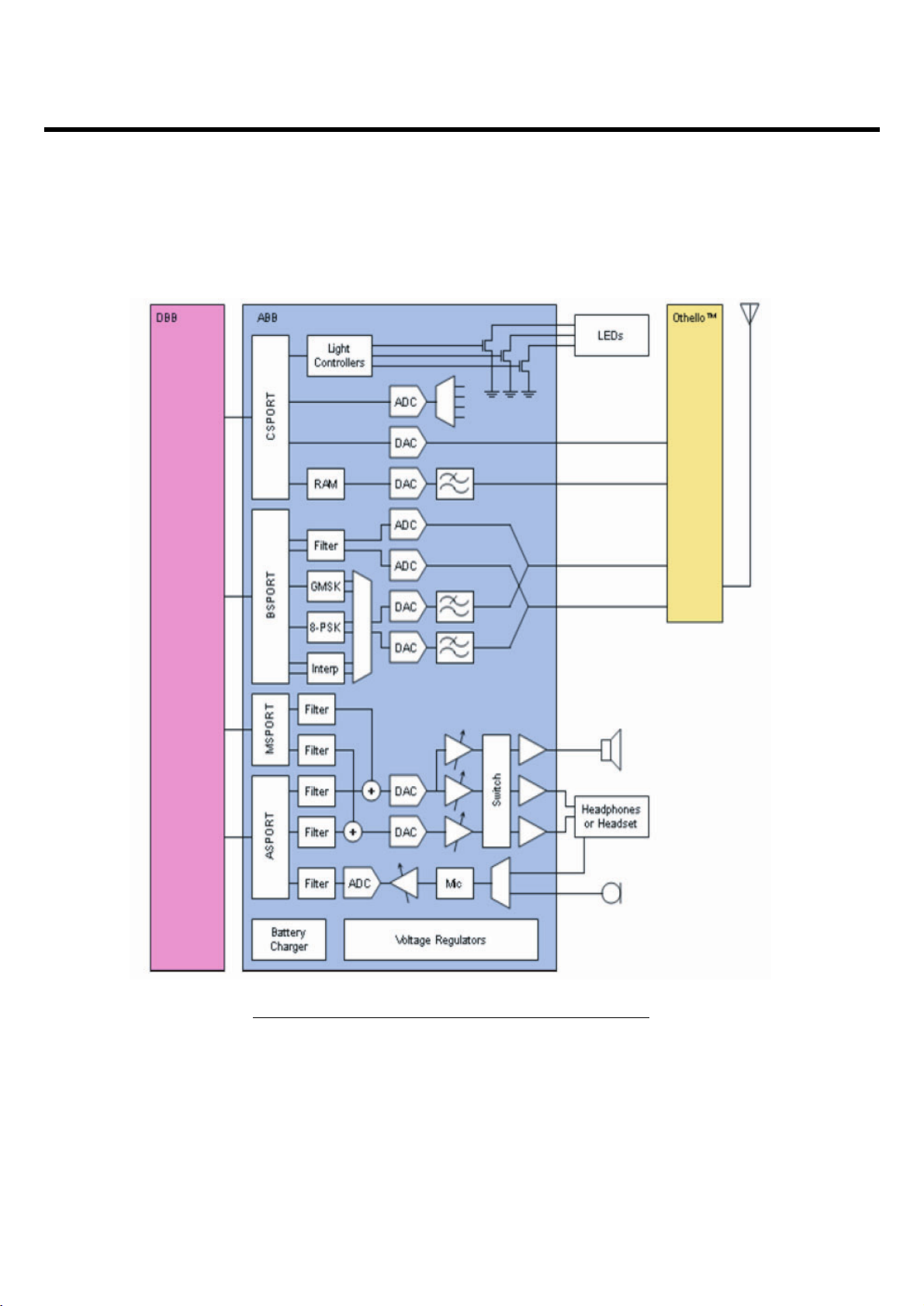
The AD6855 Audio Section supports communications and personal audio applications.
The Audio Section provides an audio codec with two digital-to-analog converters and an analog-todigital converter, a microphone interface, and analog input and output channels.
Audio and Music Serial Ports
The AD6855 Audio Serial Port is described in detail in the Audio Serial Port (ASPORT) section below.
AD6855 Music serial port (MSPORT) is described in detail in the Music Serial Port (MSPORT) section
below.
Audio Codec
The AD6855 audio codec supports communications applications with digital sample rates of 8 kHz or
16kHz. DAC 1 is used for receiving speech. An ADC is used for sending speech. The AD6855 audio
codec supports personal audio applications with digital sample rates of 8 kHz, 11.025kHz, 12 kHz, 16
kHz, 22.05 kHz, 24 kHz, 32 kHz, 44.1 kHz, or 48 kHz. DAC 1 and DAC 2 are used for monophonic
audio. The channels are common in the digital section. DAC 1 and DAC 2 are used together for stereo
audio, with DAC 1 decoding the left-channel digital input and DAC 2 decoding the right-channel digital
input.
LGE Internal Use Only
Copyright © 2008 LG Electronics. Inc. All right reserved.
Only for training and service purposes
Figure 3-15-1 ABB Internal Audio Block Diagram
Page 49

- 50 -
3. TECHNICAL BRIEF
Audio codec operating modes can be controlled by writing 5 bit codes in the AudMode field of the
AudControl1 register and in the AudMode_M field of the AudControl4 register.
AudControl1 programs the sampling rate and stereo or monophonic operating mode for PCM audio
samples input via the ASPORT.
AudControl4 programs the sampling rate and stereo or monophonic operating mode for PCM audio
samples input via the MSPORT.
The AudControl1 and AudControl4 contain control bits that allow system software to turn on three
audio loudness enhancement techniques meant for use when driving 8 ohm loudspeakers. These are
high pass filter, dynamic range compressor, and x4 gain boost.
These loudness enhancement techniques can be used with any AudMode or AudMode_M setting. And
are programmed seperately and independently for the ASPORT and MSPORT PCM audio decoder
data streams.
Analog Audio Output & Input Configurations
Output configurations are set by AudOS[4:0] bits in the AudControl2 register. Input configurations are
set by AudIS[3:0] bits in the AudControl2 register.
AudIn3LMute bit high in the AudMuteControl register (0x27). For configurations using “DAC2+AIN3R”,
the AIN3R input may be muted by setting AudIn3RMute bit high in the AudMuteControl register. For
configurations using “AIN3(L)”, the AIN3L and AIN3R inputs may be used as a differential input or the
AIN3L input may be used as a single-ended input.
Single ended configuration is chosen by setting AudIn3Cfg bit high in the AudControl3 register (0x32).
Audio DACs and Analog Filters
The Audio DACs are over-sampled switched-capacitor DACs. The analog filters are switchedcapacitor filters followed by active-RC filters.
LGE Internal Use Only
Copyright © 2008 LG Electronics. Inc. All right reserved.
Only for training and service purposes
Page 50

- 51 -
3. TECHNICAL BRIEF
Analog Audio Output Drivers
Audio Output 1
PGA gain for Audio Output 1 can be set by using bits AudOut1Gain[4:0] in the AudOut12Control
(0x21 ) register. Output 1 is used for 32ߟ interface with differential output but can be used by
single ended interface.
And this model only uses passive filters between output port and Receiver.
Audio Output 2
PGA gain for Audio Output 2 can be set by using bits AudOut2Gain[4:0] in the AudOut12Control
(0x21) register. Output 2 is used for 8ߟ. This port supports only a differential interface. And this
model only uses passive filters and Class D audio amplifier between output port and speaker. Audio
amplifier Gain is set by hardware component and gain is 6 times.
LGE Internal Use Only
Copyright © 2008 LG Electronics. Inc. All right reserved.
Only for training and service purposes
Figure 3-15-2 ABB Audio OUTPUT1
Figure 3-15-3 ABB Audio OUTPUT2
Page 51

- 52 -
3. TECHNICAL BRIEF
Audio Output 3
PGA gain for Audio Output 3 Stereo Configuration can be set by using bits AudOutLGain[4:0] and
AudOutRGain[4:0] in the AudOutLRControl (0x22) register. When Audio Output 3 configured as
monophonic differential output PGA gain can be set by using bits AudOut3Gain[4:0] in the
AudOut3Control register (0x23).
This port is used for headset speaker in stereo. This port must use DC-coupling capacitor as output
DC. It uses two 100uF capacitor each other in left and right output.
Analog Audio Input
The AD6855 provides two analog input channels, AIN1 and AIN2, that may be used for both
microphone and line inputs. The AIN1 and AIN2 channels are identical. One of the two channels is
typically used with microphone built into a handset. The other channel is typically used with an external
microphone or external line input.
LGE Internal Use Only
Copyright © 2008 LG Electronics. Inc. All right reserved.
Only for training and service purposes
Figure 3-15-3 ABB Audio OUTPUT3
Figure 3-15-4 Audio Input Block Diagram
Page 52

- 53 -
3. TECHNICAL BRIEF
Analog Input AIN1, AIN2 and VMIC configurations can be chosen by setting bits AudIS[3:0] in the
AudControl2 register (0x1E ). Additional gain of 9dB can be inserted into Analog Audio Input signal
chain by setting AudPreampGainSel bit high in the AudControl3 register (0x32 ).
Microphone Interface
The microphone pre-amplifier and associated integrated resistors support electret microphones. An
internal (Configuration 11) or external (Configuration 01 or 10) load resistor converts the current input
of the microphone to a voltage signal which is amplified using a low-noise pre-amplifier. The
Microphone signal path also includes an additional programmable gain of +9 dB gain directly after the
pre-amplifier. Different microphones require different DC bias currents for optimum sensitivity.
Audio ADC and PGA
The Audio ADC is a high-order single-bit sigma-delta ADC that includes a switchedcapacitor PGA at
the input.
Digital Filters
The AD6855 Audio Section provides two digital filters. The voiceband filter is used for applications with
a 8 kHz digital sample rate. The high-quality audio filter is used for applications with higher digital
sample rates.
Audio Accessory Detection
The AD6855 provides for detection of audio headset accessory insertion, extraction, and hookswitch
events. The detector circuit is designed to operate with minimum power in standby mode. There are
two pins dedicated to the accessory detector. AccDet is intended to interface to the external
microphone and monitor its bias voltage. The ACCDET terminal is used to sense hookswitch events
while a headset accessory is inserted. The JackSense terminal is interfaced to the switch pin of the
Jack socket or a Jack Sense terminal on a handset system connector.
LGE Internal Use Only
Copyright © 2008 LG Electronics. Inc. All right reserved.
Only for training and service purposes
Page 53

- 54 -
3. TECHNICAL BRIEF
Use of the AccDet Terminal for Hookswitch Event Detection
The AccDet terminal may be connected directly to the Ain2P pin in the case of a DC coupling of the
accessory microphone. If the accessory microphone is connected via a capacitor then the AccDet pin
may be connected to the microphone side of the coupling capacitor. The AccDet terminal is used to
detect hookswitch events. Hookswitch events cause the system to answer an incoming phone call or
hang up on an active phone call.
The detector circuit is in operation only if an accessory is inserted. It monitors the voltage at the
AccDet terminal using a comparator as shown Figure below.
Associated logic then provides the AudAccInt interrupt and updates the contents of the Detector
Control register as follows on each comparator transition.
LGE Internal Use Only
Copyright © 2008 LG Electronics. Inc. All right reserved.
Only for training and service purposes
Figure 3-15-5 Audio Accessory Detection Block Diagram
Page 54

- 55 -
3. TECHNICAL BRIEF
Use of the JackSense Terminal for Accessory Insertion and Removal Detection
Accessory insertion and removal is detected using the JackSense terminal.
The JackSense terminal is connected to a signal produced by a mechanical connection that indicates
the presence or absence of the headset accessory. The insertion/removal sense circuit fed by
JackSense is flexible as far as the characteristics of the mechanical connection are concerned. The
mechanical connection will often times be pulled down in one state and floating in the other. In such
cases a 1uA on chip current source is used to pull JsckSense to VBAT when the mechanical
connection is floating.
To avoid false interrupts the Accessory detect logic has a hardware polling loop which will prevent
Interrupt generation from comparator transitions with a duration of no less than 10 mSec.
LGE Internal Use Only
Copyright © 2008 LG Electronics. Inc. All right reserved.
Only for training and service purposes
Figure 3-15-6 Accessory Insertion/Removal Detector Block Diagram
Page 55

- 56 -
3. TECHNICAL BRIEF
3.16 Camera Interface(2M Fixed Focus Camera)
3.16.1 AD6900 Camera Interface (PPI Block)
AD6900 provides a Parallel Peripheral Interface (PPI) that can connect directly to camera modules.
The PPI is an input-only parallel external port that accommodates up to 10 bits of data, in a variety of
RGB and YUV color formats. In addition, ITU-656 (CCIR656) and ITU-601 (CCIR601) compatible data
transfers are supported.
The PPI feature set includes:
Eight dedicated data pins and two data pins muxed with GPIOs
Parallel data transfer rates up to 32.5 MB/s
Two frame syncs (horizontal and vertical), with programmable polarity
A bidirectional clock pin, with programmable output clock rate up to 65 MHz
Synchronization by detection of embedded preamble codes or by using frame synchronization pins
ITU standard and counter controlled data transfers
8-bit data packing to reduce DMA bandwidth for image data
Data re-ordering to reduce DMA bandwidth for YUV 4:2:2 data
A 32 word by 16 bit input FIFO
The PPI offers specific configurations to support still image and video data inputs.
The PPI supports ITU-601 and ITU-656 standards. It also provides Active Video Only and Entire Field
operational modes. In all modes, data packing options optimize DMA transfer bandwidth for YUV 4:2:2
and other data formats.
The PPI pins are listed in the following table.
LGE Internal Use Only
Copyright © 2008 LG Electronics. Inc. All right reserved.
Only for training and service purposes
Page 56

- 57 -
3. TECHNICAL BRIEF
PPI Architecture
A simplified PPI block diagram is shown in the following figure. The PPI contains a 32 word by 16 bit
FIFO, interrupt request (IRQ) generation logic, clock dividers, and memory mapped registers(MMRs).
The PPI provides a parallel interface to camera modules.
LGE Internal Use Only
Copyright © 2008 LG Electronics. Inc. All right reserved.
Only for training and service purposes
Bi-Directional Input Clock PPI_CLK
Input Frame Sync PPI_VSYNC
Input Frame Sync PPI_HSYNC
Input Optional Data PPI_DATA_10B_LSB[0]
Input Optional Data PPI_DATA_10B_LSB[1]
Input Data PPI_DATA[0]
Input Data PPI_DATA[1]
Input Data PPI_DATA[2]
Input Data PPI_DATA[3]
Input Data PPI_DATA[4]
Input Data PPI_DATA[5]
Input Data PPI_DATA[6]
Input Data PPI_DATA[7]
Direction Default Function Signal Name
Figure 3-16-1 PPI Block Diagram
Page 57

- 58 -
3. TECHNICAL BRIEF
FIFO Operation
The PPI FIFO is 32 words by 16 bits. Received data is stored in the FIFO either as 16- bit words or as
8-bit words. The data is only stored a 8-bit words when the DLEN and PACK_EN bits in the PPI
Control register are cleared. The data in the FIFO may be read whenever the FIFO is not empty. The
DMA controllers may burst read the FIFO data whenever at least four words are contained in the
FIFO. These FIFO status conditions are reported in the PPI Status register and can be unmasked in
the PPI DMA Interrupt Mask register to generate interrupts.
Interrupt Request Generation
The PPI generates interrupt requests for the DMA controllers, MCU, and DSP.
An interrupt can be generated for the following conditions:
Start of a frame
FIFO overflow
FIFO underflow
Incorrect number of data words in a line or lines in a frame
Preamble code error (in ITU-656 mode)
PPI Clock Frequency
The PPI transfer clock may be provided either by an external source or internally by the PPI. BCLK is
the source for the PPI clock divider. The clock may be divided by 1, 2, 3, 4, 5, 6, 7,8, 16, 32 or 64 from
BCLK. However, the maximum frequency supported is 32.5 MHz for packed 8-bit transfers and 16.25
MHz for 10-bit or unpacked 8-bit transfers. At higher clock frequencies, the APPDMA does not support
the incoming data bandwidth. A PPI FIFO (32 words deep, 16-bits wide) is provided to compensate for
arbitration latency encountered by APP DMA accessing system resources.
LGE Internal Use Only
Copyright © 2008 LG Electronics. Inc. All right reserved.
Only for training and service purposes
Page 58

- 59 -
3. TECHNICAL BRIEF
3.17 KEY BACLKLIGHT LED Interface
The AD6855 Auxiliary Section provides three independent PWM light controllers.
The PWM output controllers regulate the average current through active lights.
The output frequencies of the LIGHTx PWM output controllers are set by the Light12Period (0x2F) and
Light3Period (0x31) control registers.
With fMCLK = 13 MHz, frequencies ranging from 50.781 kHz to 49.591 Hz may be specified.
fLIGHT1 = ( fMCLK / 256 ) / ( Light12Period[9:0] + 1)
fLIGHT2 = ( fMCLK / 256 ) / ( Light12Period[9:0] + 1)
fLIGHT3 = ( fMCLK / 256 ) / ( Light3Period[9:0] + 1)
he output duty cycles of the PWM output controllers are set by the LightxDutyCycle[7:0] control
registers - Light1DutyCycle (0x2D), Light2DutyCycle (0x2E) and Light3DutyCycle (0x30).
This model use only Light3 port and 2 high luminance white LED with light guard film.
LGE Internal Use Only
Copyright © 2008 LG Electronics. Inc. All right reserved.
Only for training and service purposes
Figure 3-17 ABB Light Controller Block Diagram
Page 59

- 60 -
3. TECHNICAL BRIEF
3.18 Vibrator Interface
Vibrator is drived by Dual BJT with bias resistor.
VIBRATOR_P is connected with + terminal of vibrator and - terminal is connected with Ground. It is
controlled by VIBRATOR signal of DBB with only ON/OFF function.
LGE Internal Use Only
Copyright © 2008 LG Electronics. Inc. All right reserved.
Only for training and service purposes
T
V
Figure 3-18 Vibrator Driver Block Diagram
VBA
Q400
IBRATOR_P
R408
2.2
VIBRATOR
Q2_C
3
Q1_B
2
Q1_E
1
Q2_E
4
Q2_B
5
Q1_C
6
Page 60

4.1 RF Component
U601 Power Amp Module (SKY77318)
U602 (AD6548) RF Main Chip (Transceiver)
X601 Crystal, 26MHz Clock
FL601 FEM
- 61 -
4. TROUBLE SHOOTING
4. TROUBLE SHOOTING
LGE Internal Use Only
Copyright © 2008 LG Electronics. Inc. All right reserved.
Only for training and service purposes
TEST POINT
U601
FL601
U602
X601
Figure 4-1
Page 61

LGE Internal Use Only
Copyright © 2008 LG Electronics. Inc. All right reserved.
Only for training and service purposes
- 62 -
4. TROUBLE SHOOTING
4.2 RX Trouble
CHECKING FLOW
START
HP8960 : Test mode
62 CH, 7 level setting (TCH)
62CH, -60dBm setting (BCCH)
Spectrum analyzer setting
Oscilloscope se
tting
(1) Check
Crystal Circuit
(2) Check
Mobile SW &FE
(3) Check
RX I/Q Signa
Re-download SW or
Do calibration again
M
l
Page 62

LGE Internal Use Only
Copyright © 2008 LG Electronics. Inc. All right reserved.
Only for training and service purposes
4. TROUBLE SHOOTING
- 63 -
(1) Checking Crystal Circuit
C120(b)
C619(a)
26 MHzO.K?
NoNo
Crystal Circuit is OK
See next Page to check
Mobile
SW
See next Page to check
Mobile SW
Yes
Change 60
1
5
u
4
2
TEST POINT CHECKING FLOW
CIRCUIT
WAVEFORM
Graph 4-2-1(a)
Graph 4-2-1(b)
Figure 4-2-1
QN
82p
C617
QP
VLDO1
C618
47p
25
26
27
28
29
30
31
32
33
VLDO1
IP
C642
IN
C636
39p
82p
RX1900B
RX1900
RX1800B
RX1800
RX900B
RX900
RX850B
RX850
GND
24
1
23
VCC_BBQ
VCC_FE
2
AA12
KEY_ROW4
SIM_DATA
1
2V75_VCXO
X601
26MHz
2
34
26M
TSX-3225_26MHZ
17
22QB20
19
21
18
Q
REFIN
REFINB
REF_OP
VCC_REF
VAFC_NC
VLDO2
VLDO1
VBAT
AD6548
U602
VCC_TXVCO
TXOP_HI
TXOP_LO
VLDO3
SCLK
SDATA7SEN
VCC_BBI
I
IB
NC
6
5
4
3
8
C639
100p
C622
16
15
220n
14
13
VDD
12
11
10
9
C634
0.1u
C640
C641
100p
100p
R611
AFC
10K
C619
1u
0.1u
C620
2V93_VEXT
C626
C629
0.1u
C630
0.1u
27p
S_EN
S_CLK
S_DATA
(GPIO_072)
(GPIO_074)
(GPIO_073)
VLDO1
VBAT
C62
0.1
C627
0.1u
6M
FOLDER_DET
CAM_LDO_EN
LOUD_SPK_EN
LCD_RESET
CAM_RESET
CAM_I2C_DATA
CAM_I2C_CLK
SIM_CLK
MC_CLK
MC_CMD
MC_D0
MC_D1
MC_D2
MC_D3
LCD_WR
LCD_RS
LCD_VSYNC
CAM_PWDN
BT_LDO_EN
BT_RESET
CAM_HSYNC
CAM_VSYNC
CAM_PCLK
C120
KEYPADROW_
L19
SIMDATAIO
K19
SIMCLK
B14
1000p
CLKIN
F22
MC_CLK
J19
MC_CMD
J17
MC_DAT_0
E21
MC_DAT_1
F21
MC_DAT_2
K17
MC_DAT_3
P4
GPIO_010
P19
EB2_NRD
N17
EB2_NWE
W17
EB2_NWAIT
P21
EB2_ADDR_00
P17
EB2_ADDR_01
R19
EB2_ADDR_02
T19
EB2_ADDR_03
U22
EB2_ADDR_04
R17
EB2_ADDR_05
K21
EB2_ADDR_06
L21
EB2_ADDR_07
P22
EB2_ADDR_08
N22
EB2_ADDR_09
U19
EB2_ADDR_10
T17
EB2_ADDR_11
W18
EB2_ADDR_12
AB21
PPI_HSYNC
AA22
PPI_VSYNC
Y21
PPI_CLK
L22
Page 63

LGE Internal Use Only
Copyright © 2008 LG Electronics. Inc. All right reserved.
Only for training and service purposes
4. TROUBLE SHOOTING
- 64 -
(2) Checking Mobile SW & FEM
ANT_SW1
ANT_SW2
2V75_VCXO
2
1
TEST POINT
CIRCUIT
Figure 4-2-2
WAVEFORM
EGSM RX
ANT_SW1
ANT_SW2
Low
Low
Graph 4-2-2 FEM Control Signal
2V75_VCXO
C628
C632
0.1u
39p
R612
10
GND6
20
GND5
19
GND4
18
GND3
16
GND2
11
GND1
9
VDD
12
VC2
13
VC1
14
DGM1110M014
FL601
GSM850_900_TX
GSM1800_1900_TX
GSM1900_RX2
GSM1900_RX1
GSM1800_RX2
GSM1800_RX1
GSM900_RX2
GSM900_RX1
GSM850_RX2
ANT
GSM850_RX1
17
15
10
8
7
6
5
4
3
2
1
ANT_SW
ANT_SW
C643
100p
C644
100p
Page 64

LGE Internal Use Only
Copyright © 2008 LG Electronics. Inc. All right reserved.
Only for training and service purposes
4. TROUBLE SHOOTING
- 65 -
CHECKING FLOW
Table 4.2.1
Switch Mode Vc1 Vc2
GSM850/900 Tx 0 1
GSM1800/1900 Tx 1 1
GSM850/900 Rx 0 0
GSM1800/1900 Rx 1 0
For these 2 test case,
No Call connection is needed
Check SW601 Pin ANT,RF
with RF Cable connected.
Check SW601 Pin ANT,RF
with No RF Cable Connected
Check C643,C644,C632
Check whether Ant SW
Set as RX mode
Refer to Table 4.2.2
Check RF Level of
FL601.3(for EGSM) &
FL601.5&7(for DCS&PCS)
Open
Yes
Short
Yes
Check Vctrl 1,2 & Vcxo
Yes
Pin 16 : ~ -62dBm
Pin 14 & 12 : ~ -63dBm
Yes
Ant SW & Mobile SW is OK
See next Page to check
Rx I/Q Signal
No
No
No
No
Changing SW
Changing SW
Changing the Board.
Chang
601
601
ing FL601
For this RF Level test case,
RX Stand alone Mode is needed
refer to chapter
10
Page 65

(3) Checking RX I/Q
LGE Internal Use Only
Copyright © 2008 LG Electronics. Inc. All right reserved.
Only for training and service purposes
4. TROUBLE SHOOTING
- 66 -
TEST POINT
WAVEFORM
CIRCUIT
Graph 4-2-3
Figure 4-2-3
5
u
CHECKING FLOW
C642
SW601
U617
U602
QN
82p
C617
QP
VLDO1
C618
47p
24
23
Q
25
RX1900B
26
RX1900
VCC_BBQ
27
RX1800B
28
RX1800
29
RX900B
30
RX900
31
RX850B
32
RX850
33
GND
VCC_FE
I
1
2
VLDO1
C636
39p
IP
C642
82p
IN
22QB20
AD6548
U602
IB
3
26M
21
REF_OP
VCC_BBI
4
19
REFIN
SDATA7SEN
6
5
17
18
REFINB
VAFC_NC
VCC_TXVCO
TXOP_LO
SCLK
8
C639
100p
26MHz
VCC_REF
VLDO2
VLDO1
TXOP_HI
VLDO3
NC
1
2
34
VBAT
VDD
C640
100p
X601
TSX-3225_26MHZ
16
15
14
13
12
11
10
9
C641
100p
2V75_VCXO
R611
AFC
2V93_VEXT
C630
0.1u
S_EN
S_CLK
S_DATA
C620
C626
0.1u
0.1u
(GPIO_072)
(GPIO_074)
(GPIO_073)
10K
VLDO1
VBAT
C62
0.1
C627
0.1u
C619
1u
C622
220n
C629
27p
C634
0.1u
Check C617, C642.
Check if there is any
Major difference
Refer to graph 4.
2.3
No
No
Similar?
Yes
Redownload software and calibration again
Replace U60
2
Page 66

LGE Internal Use Only
Copyright © 2008 LG Electronics. Inc. All right reserved.
Only for training and service purposes
4. TROUBLE SHOOTING
- 67 -
4.3 TX Trouble
CHECKING FLOW
START
HP8960 : Test mode
62 CH, 7 level setting (TCH)
62CH, -60dBm setting (BCCH)
Spectrum analyzer setting
Oscilloscope se
tting
(1)Check
Crystal Circuit
(2)Check
Mobile SW
& FEM
(3)Check
PAM control
al
sign
(4)Check
TX I/Q Signal
Redownload SW or
Do calibration again
Page 67

(1) Checking Crystal Circuit
- 68 -
LGE Internal Use Only
Copyright © 2008 LG Electronics. Inc. All right reserved.
Only for training and service purposes
C120(b)
C619(a)
26 MHzO.K?
No
No
Crystal Circuit is OK
See next Page to check
Mobile
SW
See next Page to check
Mobile SW
Yes
Change 60
1
TEST POINT CHECKING FLOW
CIRCUIT
WAVEFORM
Graph 4-3-1(a)
Graph 4-3-1(b)
Figure 4-3-1
5
u
4
2
AA12
QN
82p
C617
QP
VLDO1
C618
47p
24
25
RX1900B
26
RX1900
27
RX1800B
28
RX1800
29
RX900B
30
RX900
31
RX850B
32
RX850
33
GND
1
VLDO1
C636
39p
IP
C642
82p
IN
23
VCC_BBQ
VCC_FE
2
1
2V75_VCXO
X601
26MHz
2
34
26M
TSX-3225_26MHZ
17
22QB20
19
21
18
Q
REFIN
REFINB
REF_OP
VCC_REF
VAFC_NC
VLDO2
VLDO1
AD6548
U602
VCC_TXVCO
TXOP_HI
TXOP_LO
VLDO3
SCLK
SDATA7SEN
VCC_BBI
I
IB
NC
6
5
4
3
8
C639
100p
C622
16
15
220n
14
VBAT
13
VDD
12
11
10
C629
9
27p
C634
0.1u
C640
C641
100p
100p
R611
AFC
10K
C619
1u
0.1u
C620
VLDO1
VBAT
2V93_VEXT
C62
0.1
C627
C626
0.1u
0.1u
C630
0.1u
(GPIO_072)
S_EN
(GPIO_074)
S_CLK
(GPIO_073)
S_DATA
SIM_DATA
6M
FOLDER_DET
CAM_LDO_EN
LCD_VSYNC
CAM_PWDN
BT_LDO_EN
LOUD_SPK_EN
LCD_RESET
CAM_RESET
CAM_I2C_DATA
CAM_I2C_CLK
CAM_HSYNC
CAM_VSYNC
KEY_ROW4
SIM_CLK
MC_CLK
MC_CMD
MC_D0
MC_D1
MC_D2
MC_D3
LCD_WR
LCD_RS
BT_RESET
CAM_PCLK
C120
KEYPADROW_
L19
SIMDATAIO
K19
SIMCLK
B14
1000p
CLKIN
F22
MC_CLK
J19
MC_CMD
J17
MC_DAT_0
E21
MC_DAT_1
F21
MC_DAT_2
K17
MC_DAT_3
P4
GPIO_010
P19
EB2_NRD
N17
EB2_NWE
W17
EB2_NWAIT
P21
EB2_ADDR_00
P17
EB2_ADDR_01
R19
EB2_ADDR_02
T19
EB2_ADDR_03
U22
EB2_ADDR_04
R17
EB2_ADDR_05
K21
EB2_ADDR_06
L21
EB2_ADDR_07
P22
EB2_ADDR_08
N22
EB2_ADDR_09
U19
EB2_ADDR_10
T17
EB2_ADDR_11
W18
EB2_ADDR_12
AB21
PPI_HSYNC
AA22
PPI_VSYNC
Y21
PPI_CLK
L22
Page 68

- 69 -
LGE Internal Use Only
Copyright © 2008 LG Electronics. Inc. All right reserved.
Only for training and service purposes
(2) Checking Mobile SW & FEM
TEST POINT
CIRCUIT
Figure 4-3-2
WAVEFORM
Graph 4-3-2 FEM Control Signal
2
1
ANT_SW1
ANT_SW2
2V75_VCXO
2V75_VCXO
C632
39p
C628
0.1u
R612
10
GND6
20
GND5
19
GND4
18
GND3
16
GND2
11
GND1
9
VDD
12
VC2
13
VC1
14
DGM1110M014
FL601
C643
100p
GSM850_900_TX
GSM1800_1900_TX
GSM1900_RX2
GSM1900_RX1
GSM1800_RX2
GSM1800_RX1
GSM900_RX2
GSM900_RX1
GSM850_RX2
ANT
GSM850_RX1
17
C644
100p
15
10
8
7
6
5
4
3
2
1
ANT_SW
ANT_SW
Page 69

LGE Internal Use Only
Copyright © 2008 LG Electronics. Inc. All right reserved.
Only for training and service purposes
4. TROUBLE SHOOTING
- 70 -
CHECKING FLOW
Table 4-3-1
Switch Mode Vc1 Vc2
GSM850/900 Tx 0 1
GSM1800/1900 Tx 1 1
GSM850/900 Rx 0 0
GSM1800/1900 Rx 1 0
TX Stand alone Mode is needed. Refer to
Check C643,C644,C632
Check whether Ant SW
Set as TX mode
Refer to Graph 4.3.2
Refer to Table 4.3.2
For the test,
chapter 10 (PL=7 for EGSM, PL=2 for
Check Vctrl 1,2 & Vcxo
DCS&PCS)
No
Yes
Changing boar
d
Check RF Level of
FL601.15(for EGSM) & FL601.10(for
DCS&PCS)
Check SW601.ANT, RF with RF
Cable connected.
Check SW601.ANT,RF
with RF Cable disconnected
Pin15 : ~29.5dBm
Pin10 : ~26.5dBm
Yes
Open
Yes
Short
Yes
END
No
No
No
Go to 4.3.4 Checking PAM
control sign
Changing SW
Changing SW
601
601
al
Page 70

LGE Internal Use Only
Copyright © 2008 LG Electronics. Inc. All right reserved.
Only for training and service purposes
4. TROUBLE SHOOTING
- 71 -
(3) Checking PAM Control Signal
Similar?
Yes
No
Check TX_RAMP and PAM_EN
Any Major Difference or not
¨
Similar?
Yes
No
Go to Next Step
Similar?
Yes
No
Re-download
S/W
Check if there is
Any Major Difference or not
¨
Refer to Graph 4.3.3
C614 PA_EN
C613 PA_BAND
C604 Tx_R
amp
(GPIO_060)
(GPIO_070)
0.01u
C606
DNI
C615
C604
39p
27p
C614
22u
C601
0.01u
C605
VBAT
DNI
C610
C612 4.3nH
0R613
C602
33p
27p
C613
1K R603
R610
82
C603
C616
2.7p
0.01u
0.5p
C609
51
R607
7
GND2
GND38GND4
9
10
GND512GND613GND7
GND814GND9
16
P_GND
21
19
RSVD_GND
VAPC
20
VBATT
17
2
VCC1A6VCC1B
U601
SKY77318
BS
1
3
DCS_PCS_INDCS_PCS_OUT
15
4
EGSM_IN
11
EGSM_OUT
ENABLE
18
GND1
5
TX_RAMP
PA_EN
PA_BAND
TEST POINT
CHECKING FLOW
WAVEFORM
CIRCUIT
Graph 4-3-3
Figure 4-3-3
Page 71

LGE Internal Use Only
Copyright © 2008 LG Electronics. Inc. All right reserved.
Only for training and service purposes
4. TROUBLE SHOOTING
- 72 -
(4) Checking TX I/Q
Re-download the Software
And calibrate
Check if there is
Any
Major Difference
¨
Refer to Graph4.3.4
Similar?
Yes
No
Replace U60
2
U602
U617
C642
SW601
TEST POINT
WAVEFORM
CIRCUIT
Graph 4-3-4
Figure 4-3-4
5
u
CHECKING FLOW
QN
82p
C617
QP
VLDO1
C618
47p
24
23
Q
25
RX1900B
26
RX1900
VCC_BBQ
27
RX1800B
28
RX1800
29
RX900B
30
RX900
31
RX850B
32
RX850
33
GND
VCC_FE
I
1
2
VLDO1
C636
39p
IP
C642
82p
IN
22QB20
AD6548
U602
IB
3
21
4
26M
REF_OP
VCC_BBI
5
19
18
REFIN
REFINB
VCC_TXVCO
SCLK
SDATA7SEN
6
17
VCC_REF
VAFC_NC
TXOP_HI
TXOP_LO
NC
8
C639
100p
26MHz
VLDO2
VLDO1
VLDO3
VBAT
VDD
1
X601
2
34
TSX-3225_26MHZ
16
15
14
13
12
11
10
9
C640
C641
100p
100p
2V75_VCXO
R611
AFC
2V93_VEXT
C630
0.1u
S_EN
S_CLK
S_DATA
C620
C626
0.1u
0.1u
(GPIO_072)
(GPIO_074)
(GPIO_073)
10K
VLDO1
VBAT
C62
0.1
C627
0.1u
C619
1u
C622
220n
C629
27p
C634
0.1u
Page 72

4.4 Power On Trouble
LGE Internal Use Only
Copyright © 2008 LG Electronics. Inc. All right reserved.
Only for training and service purposes
4. TROUBLE SHOOTING
- 73 -
V
V
1
TEST POINT
CIRCUIT
Figure 4-4
E
N
P
2V75_VCX
2V93_VEXT
VCORE
O
2V5_VABB
U100
2V5_VMIC
R101
1V5_VPLL
2V85_VSIM
1V8_VRTC
1V8_VG
P
1V82_VINT
1V88_VMEM
D100
2V93_VEXT
1V88_VMEM
2V5_VABB
A3
VEXT1
B3
VEXT2
L4
VMEMOUT1
M4
VMEMOUT2
G12
VABB
F12
VPLL
F2
COREPWR2
F1
COREPWR1
E1
VCORESW1
VCORESW2
VINTOUT
VINT
VAPPGATE
VUSB
VSIM
VMIC
VRF
VGP
PA
IP
IN
QP
QN
L100 4.7uH
E2
K1
K2
D12
C11
M6
J12
C12
M5
A8
TX_RAMP
VBAT
A9
IP
A10
IN
A12
QP
A11
QN
1u
FB100
1V5_VPLL
VBAT
VCORE
1V82_VINT
C123
C122C121
C132
1u
2.2u
C125
1u
22u
22u
(2012)
C126
1u
VUSB
C127
1u
PWRON
XT_PWRON
2V85_VSIM
2V5_VMIC
C128C124
1u
2V75_VCXO
1u
C130C129
1u
1V8_VGP
D100
1
2
KDR331V
3
R101
100K
RPWRO
VBAT
END
KB422
10K
R406
OWERKEY
C13
1u
KEY_ROW4
POWERKEY
L10
M10
KEYOUT
KEYON
Page 73

LGE Internal Use Only
Copyright © 2008 LG Electronics. Inc. All right reserved.
Only for training and service purposes
4. TROUBLE SHOOTING
- 74 -
CHECKING FLOW
START
Check Battery Voltage
> 3.35V
YES
Push power-on key
And check the level change
into low of POWERKEY
YES
Check the voltage of
The LDO outputs at U
Logic level at
RPWRON(DBBON) of D100
= HIGH(above 1.2V)
100
YES
?
YES
NO
NO
NO
VCORE=1.2V~1.5V 2V75_VCXO=2.75V
1V88_VMEM=1.88V 2V85_VSIM= 2.85V
2V93_VEXT=2.93V 1V5_VPLL=1.5V
2V5_VMIC=2.5V 2V5_VABB=2.5V
NO
Charge or Change Battery
Check the contact of power key
Or dome-switc
Replace U100
Re-download software
h
Is the phone power on?
YES
The phone will
Properly operati
ng.
NO
Replace U100 and Re-download software
Does it work properly?
NO
Replace the main board
Page 74

- 75 -
4. TROUBLE SHOOTING
LGE Internal Use Only
Copyright © 2008 LG Electronics. Inc. All right reserved.
Only for training and service purposes
4.5 Charging Trouble
TEST POINT
(GPIO_037)
(GPIO_059)
(1%)
R216
10K
R213
36K
R214
100K
R212
100K
CHG_ABB
R210
10K
VUSBIN
BAT
10
CRDL
1
8
GND
9
ICDL
6
IMIN
PGND
11
2
USB
USBON
7
4
_CHG
_EN
5
_PPR
3
ISL6299U203
C215
1u
VBAT
USB_DET
CHG_EN
(GPIO_013)
30K
R217
IN3
5
11
NC1
NC2
12
OUT1
6
7
OUT2
_EN
10
3
_FLAG
VCHARGE
NCP348MTR2GU204
GATE
8
9
GATE_OUT
GND
2
1
IN1
4
IN2
CHG_ABB
R211
30K
CHG_DET
CIRCUIT
Figure 4-5
CN300
U204
C310
R213
U203
Page 75

LGE Internal Use Only
Copyright © 2008 LG Electronics. Inc. All right reserved.
Only for training and service purposes
4. TROUBLE SHOOTING
- 76 -
CHECKING FLOW
START
Change the battery
Battery is charged?
NO
Is I/O Connector(CN300)
at pin6 of U204 = 5.1V?
Is Voltage across R213
soldered ?
well-
YES
Check the voltage at
C310 = 5.
Is the voltage
about 1.2V
1V ?
YES
YES
?
YES
YES
NO
NO
NO
NO
Charging is
properly operati
Resolder the CN300
(Pin 12,13 : VCHARGE)
The TA is out of order
Change the TA
Replace the
U204
Replace the
U203
ng
Battery is charged?
YES
Charging is
properly operati
ng
NO
Replace the main board
Page 76

LGE Internal Use Only
Copyright © 2008 LG Electronics. Inc. All right reserved.
Only for training and service purposes
4. TROUBLE SHOOTING
- 77 -
4.6 Vibrator Trouble
TEST POINT
T
V
CIRCUIT
Figure 4-6
LCD Module
VIBRATOR
Vibrator PAD
PIN
1
Q400
3
2
1
Q400
Q2_C
Q1_B
Q1_E
IBRATOR_P
VIBRATOR
R408
2.2
Q2_E
Q2_B
Q1_C
VBA
4
5
6
Page 77

- 78 -
4. TROUBLE SHOOTING
LGE Internal Use Only
Copyright © 2008 LG Electronics. Inc. All right reserved.
Only for training and service purposes
CHECKING FLOW
SETTING : Enter the engineering mode, and set vibrator on at vibration of BB test menu
START
Is the voltage at pin 2
of Q400 hi
S
YE
Is the voltage at pin 4
of Q400 high (VBAT
YES
Check the soldering
of vibrator
Replace vibrator
Working well !
gh?
?
YES
YES
Vibrator
) ?
NO
NO
Check the soldering
Q400
Check the soldering
of Q400
NO
Resolder or Replace vibrator
Page 78

- 79 -
4. TROUBLE SHOOTING
LGE Internal Use Only
Copyright © 2008 LG Electronics. Inc. All right reserved.
Only for training and service purposes
4.7 LCD Trouble
TEST POINT
Figure 4-7
FL508
FL505
CN500
FL507
R504
R503
FL504
FL501
LCD Connector
CN802
U501
CN803
C519
Page 79

LGE Internal Use Only
Copyright © 2008 LG Electronics. Inc. All right reserved.
Only for training and service purposes
4. TROUBLE SHOOTING
- 80 -
C
4
5
1
0
8
9
2
3
CIRCUIT
D
L
FPCB CONNECTOR
LCD_VSYNC
CAM_VSYNC
CAM_HSYNC
CAM_RESET
CAM_DATA7
CAM_DATA6
CAM_DATA5
CAM_DATA4
CAM_DATA3
CAM_DATA2
CAM_DATA1
CAM_DATA0
CAM_MCLK
CAM_PCLK
CAM_I2C_CLK
AM_I2C_DATA
LCD_MAIN_CS
LCD_SUB_CS
LCD_WR
LCD_RS
MLED3
MLED4
MLED5
2V8_IOVDD
R501
4.7K
2V93_VEXT
C503
C504
0.1u
56p
ICVE10184E150R500FRFL500
9
INOUT_B1
8
INOUT_B2
7
INOUT_B3
6
INOUT_B4
ICVE10184E150R500FRFL502
9
INOUT_B1
8
INOUT_B2
7
INOUT_B3
6
INOUT_B4
5G110
INOUT_A4
4
INOUT_A3
3
INOUT_A2
2
INOUT_A1
1
ICVE10184E150R500FRFL503
R502
4.7K
INOUT_A4
4
INOUT_A3
3
INOUT_A2
2
INOUT_A1
1
FL506 ICVE10184E150R500FR
5G110
INOUT_A4
4
INOUT_A3
3
INOUT_A2
2
INOUT_A1
1
G15G2
INOUT_A1
INOUT_A2
INOUT_A3
INOUT_A4
G110G2
INOUT_A1
INOUT_A2
INOUT_A3
INOUT_A4
G110G2
G2
INOUT_B4
INOUT_B3
INOUT_B2
INOUT_B1
10
INOUT_B4
INOUT_B3
INOUT_B2
INOUT_B1
G2
INOUT_B4
INOUT_B3
INOUT_B2
INOUT_B1
ICVE10184E150R101FRFL508
RCV_N
RCV_P
CAM_PWDN
ZD501
RSB6.8CST2R
1
2
3
4
5
1
2
3
4
5
6
7
8
9
6
7
8
9
6
7
8
9
KEY_ROW4
KEY_ROW5
C500
DNI
C501
C502
39p
39p
L500
L501
18nH
18nH
CN500
G1G2
60
1
59
2
58 3
57
4
5
56
6
55
7
54
8
53
9
52
51
10
50
11
12
49
13
48
14
47
46
15
45
16
44
17
43
18
19
42
20
41
21
40
22
39
23
38
24
37
25
36
26
35
27
34
28
33
29
32
3031
G3G4
1V8_DVDD
C508 C509
2V8_IOVDD
0.1u0.1u
2V8_AVDD
C510
0.1u
KEY_COL3
KEY_COL4
VIBRATOR_P
MLED
100ohm R504
R505
DNI
VA501
ICVN0505X150FR
C511
C522
27p
DNI
LCD_RESET
C521
DNI
D502
D501
RSB6.8CST2R
10
G15G2
INOUT_A4
INOUT_B4
4
INOUT_A3
INOUT_B3
3
INOUT_A2
INOUT_B2
2
INOUT_A1
INOUT_B1
1
FL501 ICVE10054E250R201FR
5G110
G2
INOUT_B4
INOUT_A4
4
INOUT_A3
INOUT_B3
3
INOUT_A2
INOUT_B2
2
INOUT_A1
INOUT_B1
1
ICVE10054E250R201FRFL504
10
G15G2
INOUT_A4
INOUT_B4
4
INOUT_A3
INOUT_B3
3
INOUT_A2
INOUT_B2
2
INOUT_A1
INOUT_B1
1
FL505 ICVE10054E250R201FR
5G110
RSB6.8CST2R
G2
INOUT_A4
INOUT_B4
4
INOUT_A3
INOUT_B3
3
INOUT_B2
INOUT_A2
2
INOUT_B1
INOUT_A1
1
ICVE10054E250R201FRFL507
LCD_DATA1
6
LCD_DATA1
7
LCD_DATA1
8
LCD_DATA1
9
LCD_DATA1
6
LCD_DATA1
7
LCD_DATA0
8
LCD_DATA0
9
LCD_DATA07
6
LCD_DATA06
7
LCD_DATA05
8
LCD_DATA04
9
LCD_ID_L
MLED2
MLED1
LCD_DATA03
6
LCD_DATA02
7
LCD_DATA00
8
LCD_DATA01
9
D506
D505
D504
RSB6.8CST2R
RSB6.8CST2R
RSB6.8CST2R
LCD BACKLIGHT
10
15
4
5
9
3
C1+
C1-
IN
EN_SET
GND
PGND
AAT3169IFO-T1U501
OUTCP
C2+
C2-
D1
D2
D3
D4
D5
D6
1u
C517
VBAT
CD_BACKLIGHT_CTRT
C520
1u
R503
100K
C518
7
1u
8
6
11
12
13
14
1
2
MLED1
MLED2
MLED3
MLED4
MLED5
C519
1u
MLE
D503
RSB6.8CST2R
Page 80

LGE Internal Use Only
Copyright © 2008 LG Electronics. Inc. All right reserved.
Only for training and service purposes
4. TROUBLE SHOOTING
- 81 -
Waveform
Graph 4-7-1. LCD Backlight Control Signal Waveform
Graph 4-7-2. LCD Data Waveform
Page 81

- 82 -
4. TROUBLE SHOOTING
LGE Internal Use Only
Copyright © 2008 LG Electronics. Inc. All right reserved.
Only for training and service purposes
CHECKING FLOW
START
Is the connection of
CN802 with LCD
connector ok ?
YES
Is the connection of
CN803 with CN500
connector ok ?
YES
Check the
Voltage Level of
C519 is about Battery voltage ?
(LCD_BACKLIGHT_CTRT signal
is high Level)
YES
Check the Waveform of
EMI filter ?
YES
NO
NO
NO
NO
Reassemble FPCB with LCD connector
Reassemble FPCB with Main connector
Resoldering or Replace U501
Resolde
(FL501,FL504,
ring EMI filter.
FL505,FL507,FL508)
Check the Waveform of
Data pins on CN802 ?
LCD working well !
YES
Does LCD work
properly ?
YES
NO
NO
Replace Main FPCB
Replace LCD module
Page 82

- 83 -
4. TROUBLE SHOOTING
LGE Internal Use Only
Copyright © 2008 LG Electronics. Inc. All right reserved.
Only for training and service purposes
4.8 Camera Trouble
TEST POINT
Figure 4-8
R501
R502
FL503
FL502
FL500
FL506
U500
CN500
C523
Camera Connector
CN701
CN801
CN702
C506
C507
FB500
CN803
Page 83

LGE Internal Use Only
Copyright © 2008 LG Electronics. Inc. All right reserved.
Only for training and service purposes
4. TROUBLE SHOOTING
- 84 -
CIRCUIT
C
4
5
1
0
8
9
2
3
3
C
FPCB CONNECTOR
LCD_VSYNC
CAM_VSYNC
CAM_HSYNC
CAM_RESET
CAM_DATA7
CAM_DATA6
CAM_DATA5
CAM_DATA4
CAM_DATA3
CAM_DATA2
CAM_DATA1
CAM_DATA0
CAM_MCLK
CAM_PCLK
CAM_I2C_CLK
AM_I2C_DATA
LCD_MAIN_CS
LCD_SUB_CS
LCD_WR
LCD_RS
MLED3
MLED4
MLED5
2V8_IOVDD
R501
4.7K
2V93_VEXT
C503
C504
0.1u
56p
ICVE10184E150R500FRFL500
9
INOUT_B1
8
INOUT_B2
7
INOUT_B3
6
INOUT_B4
ICVE10184E150R500FRFL502
9
INOUT_B1
8
INOUT_B2
7
INOUT_B3
6
INOUT_B4
5G110
INOUT_A4
4
INOUT_A3
3
INOUT_A2
2
INOUT_A1
1
ICVE10184E150R500FRFL503
R502
4.7K
G15G2
INOUT_A4
4
INOUT_A3
3
INOUT_A2
2
INOUT_A1
1
FL506 ICVE10184E150R500FR
5G110
INOUT_A4
4
INOUT_A3
3
INOUT_A2
2
INOUT_A1
1
CAM_PWDN
ZD501
RSB6.8CST2R
INOUT_A1
INOUT_A2
INOUT_A3
INOUT_A4
G110G2
5
INOUT_A1
INOUT_A2
INOUT_A3
INOUT_A4
G110G2
5
G2
INOUT_B4
INOUT_B3
INOUT_B2
INOUT_B1
10
INOUT_B4
INOUT_B3
INOUT_B2
INOUT_B1
G2
INOUT_B4
INOUT_B3
INOUT_B2
INOUT_B1
ICVE10184E150R101FRFL508
RCV_N
RCV_P
C500
DNI
C501
C502
39p
39p
L500
L501
18nH
18nH
CN500
1
2
3
4
KEY_ROW4
1
2
3
4
6
7
8
9
6
7
8
9
6
7
8
9
KEY_ROW5
60
59
58 3
57
56
55
54
53
52
51
50
49
48
47
46
45
44
43
42
41
40
39
38
37
36
35
34
33
32
G1G2
1
2
4
5
6
7
8
9
10
11
12
13
14
15
16
17
18
19
20
21
22
23
24
25
26
27
28
29
3031
G3G4
1V8_DVDD
C508 C509
2V8_IOVDD
0.1u0.1u
2V8_AVDD
C510
0.1u
KEY_COL3
KEY_COL4
VIBRATOR_P
MLED
100ohm R504
R505
DNI
VA501
ICVN0505X150FR
C511
C522
27p
DNI
LCD_RESET
C521
DNI
D502
D501
RSB6.8CST2R
10
G15G2
INOUT_A4
INOUT_B4
4
INOUT_A3
INOUT_B3
3
INOUT_A2
INOUT_B2
2
INOUT_A1
INOUT_B1
1
FL501 ICVE10054E250R201FR
5G110
G2
INOUT_B4
INOUT_A4
4
INOUT_A3
INOUT_B3
3
INOUT_A2
INOUT_B2
2
INOUT_A1
INOUT_B1
1
ICVE10054E250R201FRFL504
10
G15G2
INOUT_A4
INOUT_B4
4
INOUT_A3
INOUT_B3
3
INOUT_A2
INOUT_B2
2
INOUT_A1
INOUT_B1
1
FL505 ICVE10054E250R201FR
5G110
RSB6.8CST2R
G2
INOUT_A4
INOUT_B4
4
INOUT_A3
INOUT_B3
3
INOUT_B2
INOUT_A2
2
INOUT_B1
INOUT_A1
1
ICVE10054E250R201FRFL507
LCD_DATA1
6
LCD_DATA1
7
LCD_DATA1
8
LCD_DATA1
9
LCD_DATA1
6
LCD_DATA1
7
LCD_DATA0
8
LCD_DATA0
9
LCD_DATA07
6
LCD_DATA06
7
LCD_DATA05
8
LCD_DATA04
9
LCD_ID_L
MLED2
MLED1
LCD_DATA03
6
LCD_DATA02
7
LCD_DATA00
8
LCD_DATA01
9
D506
D505
D504
RSB6.8CST2R
RSB6.8CST2R
RSB6.8CST2R
CAMERA POWER
VBAT
RT9011-MGPQWU500
18
VIN
EN1
EN2
NC1
PGND
9
VOUT1
VOUT2
NC2
GND
AM_LDO_EN
(EB2_ADDR_00)
R500
100K
C505
1u
2
3
1V8_DVDD
7
6
54
2V8_IOVDD
C506
2.2u
C507
1u
2V8_AVDD
FB500
C52
2.2u
Page 84

LGE Internal Use Only
Copyright © 2008 LG Electronics. Inc. All right reserved.
Only for training and service purposes
4. TROUBLE SHOOTING
- 85 -
Waveform
Graph 4-8-1 I2C Data Waveform Graph 4-8-2 MCLK Waveform
Graph 4-8-3 CAM_VSYNC vs.
CAM_HSYNC Waveform
Graph 4-8-4 CAM_HSYNC vs.
CAM_PCLK Waveform
Page 85

LGE Internal Use Only
Copyright © 2008 LG Electronics. Inc. All right reserved.
Only for training and service purposes
4. TROUBLE SHOOTING
- 86 -
CHECKING FLOW
START
Is the connection of
CN702 with Camera
connector ok ?
YES
Is the connection of
CN801 with CN701
connector ok ?
YES
Is the connection of
CN803 with CN500
connector ok ?
YES
Check the
each voltage Level of
C506(1.8V), C507(2.8V), C523(2.8V)
is right ?
(CAM_LDO_EN
is
signal
high Level)
YES
Check the Waveform of
I2C_CLK, I2C_DATA ?
S
YE
Check the Waveform of
CAM_MCLK(13MHz) ?
NO
Reassemble KEY PCB
with camera connector.
NO
Reassemble FPCB
with KEY PCB connector
NO
NO
NO
NO
Reassemble FPCB with Main connector
Resoldering or Replace U500
Resoldering R501, R502
Replace U101 or Change the board
Check the Waveform of
Data pins on CN701 ?
Check the Waveform of
Does Camera work
Cam era working well !
YES
S
YE
EMI filter ?
YE
S
properly ?
YES
NO
NO
NO
Replace Camera Module.
Resoldering EMI filter.
(FL500,FL502,FL50
3,FL506)
Replace U101 or Change the board
Page 86

LGE Internal Use Only
Copyright © 2008 LG Electronics. Inc. All right reserved.
Only for training and service purposes
4. TROUBLE SHOOTING
- 87 -
4.9 Speaker Trouble
TEST POINT
A
A
A
A
T
T
S
CIRCUIT
Figure 4-9
R314
R313
U100
AOUT1N
AOUT1P
OUT2N_1
OUT2N_2
OUT2P_1
OUT2P_2
AOUT3R
AOUT3L
TDO
TMS
TCK
TDI
F11
E11
L8
M8
L9
M9
G10
F10
C2
C1
B1
D1
39p
39p
C153C151
39p
C154
C155C152
DNI
C156
DNI39p
U303
C158
100p
RCV_N
RCV_P
SPK_N
SPK_P
HP_ROU
HP_LOU
PEAKER
VBAT
(GAIN x6)
R314 47K
SPK_N
SPK_P
0.01uC316
C317 0.01u
LOUD_SPK_EN
47KR315
R317
100K
D1
C1
A1
IN-
IN+
_SD
TPA2005D1ZQYRU303
GND1
GND2
GND3
A2
A3
B3
C2
GND4
GND5D2GND6
C3
VDD1
VDD2
VO-
VO+
D3
NC
GND7
B4
C4
B1
A4
D4
C319
10u
FB304
FB305
C320
DNI
C321
1000p
C322
1000p
EVLC14S02050
VA304
CN302
1
2
VA305
EVLC14S02050
Page 87

LGE Internal Use Only
Copyright © 2008 LG Electronics. Inc. All right reserved.
Only for training and service purposes
4. TROUBLE SHOOTING
- 88 -
CHECKING FLOW
START
Check the state of
contact of spea
Yes
Check the Audio signal
R313,R314
Yes
Check the Power voltage
U303 = VBAT
And work properly ?
Yes
Speaker
Working well!
ker
!
No
No
No
Replace/Change speaker
Change the U100
Change the Speaker
Page 88

LGE Internal Use Only
Copyright © 2008 LG Electronics. Inc. All right reserved.
Only for training and service purposes
4. TROUBLE SHOOTING
- 89 -
4.10 Earphone Trouble
TEST POINT
CIRCUIT
H
T
Figure 4-10
1
V
J
P
N
R307
R309
C302
C331
C158
C303
R300
R302
C142
U100
U304
FB300
FB301
FB302
CN300
L301
2V5_VJACK
R300
1.5K
C300
10u
HP_LOUT
HP_EN
2V93_VEXT
R305
100K
R302
2.2K
R306
100K
MIC_P
MIC_N
HP_MIC_
HP_MIC_
C301
39p
HP_MIC_P
2V93_VEXT
U301
NLAS5223BMNR2G
10
NO21VCC
100u
C302
9
2
NO1
3
4
5
JACK_DETECT
EXT_PWRON
DSR_DET
(TX)
(RX)
JACK_DETECT
COM2
8
COM1
IN2
7
IN1
NC2
6
GND
NC1
USC2
USC1
C139
0.1u
0.1uC142
AIN1P
AIN1N
ACKSENSE
AIN2N
AIN2P
100uC303
R304
C304
100K
1u
MULTI_PORT_TX
MULTI_PORT_RX
M11
M12
K9
L12
L11
P_ROUT
HP_EN
(GPIO_009)
C332
DNI
EXT_PWRON
DSR
TX
RX
DNIR303
R307 4.7
R309 4.7
R311 47
47R310
HOOK_DETECTHP_MIC_N
VA300
VA301
EVLC5S0250
VUSBIN VBAT
R312
1
ZD300
C309
C308
47p
1u
EVLC5S0250
FB301
FB302
L301 100nH
VA303
C307
10u
RSB6.8CST2R
JACK_LDO_EN
VCHARGE
1800FB300
C310
1u
EVLC14S02050
R329
100K
CN300
21
19
1
2
3
4
5
6
7
8
9
10
11
12
13
14
15
16
17
18
20
22
C311
47p
U304 R1114D251D
1
VDD VOUT
4
NC
6
CE
C330 C33
1u
C305
L300
10p
270nH
GND1
GND2
FM_AN
2V5_VJACKVBAT
3
2
5
1u
Page 89

LGE Internal Use Only
Copyright © 2008 LG Electronics. Inc. All right reserved.
Only for training and service purposes
4. TROUBLE SHOOTING
- 90 -
CHECKING FLOW
START
Resolder CN300
Check the
pin(#8) in CN300 is LO
S
YE
Is FB303(JACK DETECT)
LOW?
YES
Set the audio part of the test
equipment to PRBS or
Continuous wave m
Can you hear
the sound from
the earphone?
YE
S
Set the audio part of the test
Equipment to echo m
Can you hear your
voice from
the earphone?
W?
ode
ode
NO
NO
NO
Change the earphone
and try again
NO
Change the earphone
and try again
Resolder pin8 in CN300
Resolder FB303
Can you hear
the sound from
the earphone?
YE
S
Can you hear your
voice from
the ea
rphone?
NO
NO
Resolder C302, C303, R307 &
, FB301&FB302
R309
Resolder C142,FB300, R300 &
R302
Or Change the U304 &U100
Earphone will work properly
YES
Page 90

4.11 Receiver Trouble
LGE Internal Use Only
Copyright © 2008 LG Electronics. Inc. All right reserved.
Only for training and service purposes
4. TROUBLE SHOOTING
- 91 -
TEST POINT
A
A
A
A
T
T
Figure 4-11
CIRCUIT
L500
L501
AOUT1N
AOUT1P
OUT2N_1
OUT2N_2
OUT2P_1
OUT2P_2
AOUT3R
AOUT3L
TDO
TMS
TCK
TDI
F11
E11
L8
M8
L9
M9
G10
F10
C2
C1
B1
D1
U100
RCV_N
C500
DNI
RCV_P
CAM_PWDN
RCV_N
RCV_P
SPK_N
SPK_P
HP_ROU
C158
100p
HP_LOU
C154
C153C151
39p
39p
39p
C156
C155C152
DNI39p
DNI
C501
39p
C502
39p
L500
18nH
L501
18nH
60
59
58 3
57
56
CN500
2V8_IOVDD
2V8_AVDD
1V8_DVDD
G1G2
1
2
4
Page 91

LGE Internal Use Only
Copyright © 2008 LG Electronics. Inc. All right reserved.
Only for training and service purposes
4. TROUBLE SHOOTING
- 92 -
CHECKING FLOW
SETTING : After initialize Agilent 8960, Test GSM850, PCS mode
Set the property of audio as PRBS or continuous wave. Set the receiving volume of mobile as Max.
START
Does waveform at
L500 and L501
fluctuate
?
YES
Is receiver connected
Properly?
YE
S
Receiver will work properly.
NO
NO
Change the U100
Resolder/Change the receiver
Page 92

LGE Internal Use Only
Copyright © 2008 LG Electronics. Inc. All right reserved.
Only for training and service purposes
4. TROUBLE SHOOTING
- 93 -
4.12 Microphone Trouble
TEST POINT
CIRCUIT
0
M
M
Figure 4-12
R235
R233
R317
IC_P
IC_N
MIC
C328
39p
R324
100ohm
R326
100ohm
MIC200
2V5_VMIC
1K
R318
2.2K
R322
2.2K
R327
C326
39p
C327
10u
VA306
EVLC14S02050
VA307
EVLC14S02050
C139
OBG-415L42-C33LH
MIC30
Page 93

LGE Internal Use Only
Copyright © 2008 LG Electronics. Inc. All right reserved.
Only for training and service purposes
4. TROUBLE SHOOTING
- 94 -
CHECKING FLOW
SETTING : After initialize Agilent 8960, Test GSM850, PCS mode
START
Check microphone sound hole
Make a phone call,
then check R317 mic bias signal
comes from U
YES
Check the signal
Level at each side
of MIC300.
Is it a few tens
YE
Check the soldering of
R323, R325 & C139
YES
Microphone will work
100?
mV AC?
S
properly.
NO
NO
1. Check mic Bias signal line
2. Change the U100
Change the microphone
NO
Resolder component
Page 94

LGE Internal Use Only
Copyright © 2008 LG Electronics. Inc. All right reserved.
Only for training and service purposes
4. TROUBLE SHOOTING
- 95 -
4.13 SIM Card Interface Trouble
TEST POINT
TEST POINT
)
T
S
K
Figure 4-13
PIN6 PIN4
C318
IM_DATA SIM_CL
2V85_VSIM
R316
15K
C323
DNI
PIN1 PIN3
(5000-6T-1.8SL)
4
C5
5
C6
6
C7
10
9
GND4
GND1
GND2GND3
J300
J300
2V85_VSIM
1
C1
2
C2
3
C3
7
8
C318
220n
C324
22p
C325
1000p
(GPIO_100
SIM_RS
Page 95

- 96 -
4. TROUBLE SHOOTING
LGE Internal Use Only
Copyright © 2008 LG Electronics. Inc. All right reserved.
Only for training and service purposes
CHECKING FLOW
START
Does the SIM card
support 3V or 1.8V
YES
Is Voltage at the pin1
of J300 2.85V or 1.8V
YES
Change the SIM Card
And try again.
Does it work
Properly?
S
YE
NO
?
?
This phone supports 3V or 1.8V SIM card
NO
NO
Change the SIM Card.
Voltage output
of VSIM LDO
Is 2.
85V?
YES
Resolder J300
Redownload SW.
Does it work
YES
Properly
?
NO
NO
.
Change the U100
Change the main board
SIM card is properly working
SIM card is properly working.
Page 96

- 97 -
4. TROUBLE SHOOTING
LGE Internal Use Only
Copyright © 2008 LG Electronics. Inc. All right reserved.
Only for training and service purposes
4.14 KEY backlight Trouble
TEST POINT
Figure 4-14
TOP
LD400 LD401
BOTTOM
VA400R400VA401R401
Page 97

- 98 -
4. TROUBLE SHOOTING
LGE Internal Use Only
Copyright © 2008 LG Electronics. Inc. All right reserved.
Only for training and service purposes
V
3
CIRCUIT
CHECKING FLOW
BAT
LEWWS44-E
LEWWS44-E
LD400
LD401
VA400
ICVN0505X150FR
START
Is the level Period at VA400,
VA401 Low Duty(20%)
?
VA401
ICVN0505X150FR
NO
R400
KEY_BACKLIGHT
47
R401
47
Check U100
YES
Is the level Period at VA400,
VA401 High Duty(80%)?
NO
Check U100
YES
NO
Check the soldering
each R and LE
D
NO
Replace or resolder
com
ponent
Are all LEDs
ing?
Work
YES
Backlight will work properly.
Page 98

- 99 -
4. TROUBLE SHOOTING
LGE Internal Use Only
Copyright © 2008 LG Electronics. Inc. All right reserved.
Only for training and service purposes
4.15 RTC Trouble
TEST POINT
CIRCUIT
1
2
3
4
5
6
7
8
9
3
Figure 4-15
X100
X100
FC-135
2.768KHz
R103
12
C141
22p
R104
DNI
C135
22p
R103
10M
CAM_DATA0
CAM_DATA1
CAM_DATA2
CAM_DATA3
CAM_DATA4
CAM_DATA5
CAM_DATA6
CAM_DATA7
BT_UART_TX
BT_UART_RX
BT_UART_CTS
BT_UART_RTS
M22
N21
M21
V22
V21
W22
W21
V19
Y22
A17
A16
M4
M1
M2
N6
PPI_DATA_
PPI_DATA_
PPI_DATA_
PPI_DATA_
PPI_DATA_
PPI_DATA_
PPI_DATA_
PPI_DATA_
PPI_DATA_
OSCIN
OSCOUT
L1
GPIO_000
GPIO_001
GPIO_002
GPIO_003
GPIO_004
Page 99

- 100 -
4. TROUBLE SHOOTING
LGE Internal Use Only
Copyright © 2008 LG Electronics. Inc. All right reserved.
Only for training and service purposes
CHECK FLOW
START
Is frequency
at R103 about 32.768KHz?
YES
Is voltage
at R103 about 400mV
YES
Is RTC properly working?
YES
RTC will work properly
?
NO
NO
NO
Resolder the X100 or
change the
Resolder the X100 or
change the X100
Re-download software and try
aga
X100
in
Page 100

- 101 -
4. TROUBLE SHOOTING
LGE Internal Use Only
Copyright © 2008 LG Electronics. Inc. All right reserved.
Only for training and service purposes
4.16 Folder on/off Trouble
TEST POINT
CIRCUIT
2
T
Figure 4-16
U400
V93_VEXT
C402
1u
2
1
VDD
VSS
NC OUT
4
3
EM-0781-T5
R407
R407
FOLDER_DE
0
U400
VA405
ICVN0505X150FR
 Loading...