

Service Manual
Model : HB620(T)/KB620
Service Manual
HB620(T)/KB620
Date: June, 2008 / Issue 1.0
Internal Use Only
Z3X-BOX.COM

- 3 -
1. INTRODUCTION .............................. 5
1.1 Purpose................................................... 5
1.2 Regulatory Information............................ 5
2. PERFORMANCE...............................7
2.1 System Overview .....................................7
2.2 Usable environment .................................8
2.3 Radio Performance ..................................9
2.4 Current Consumption.............................16
2.5 RSSI BAR ..............................................16
2.6 Battery BAR ...........................................16
2.7 Sound Pressure Level............................17
2.8 Charging ................................................18
3. TECHNICAL BRIEF ........................19
3.1 General Description ...............................19
3.2 GSM Mode.............................................21
3.3 UMTS Mode...........................................24
3.4 LO generation and distribution circuits...26
3.5 Off-chip RF Components .......................27
3.6 Digital Baseband (DBB/MSM6280)........43
3.7 Subsystem(MSM6280) ..........................45
3.8 Power Block ...........................................54
3.9 External memory interface .....................59
3.10 H/W Sub System..................................61
3.11 Feature List ..........................................72
4. TROUBLE SHOOTING ...................75
4.1 Power on trouble....................................75
4.2 USB trouble............................................77
4.3 SIM detect trouble..................................78
4.4 Key sense trouble (KEYPAD) ................79
4.5 Keypad backlight trouble........................81
4.6 Micro SD trouble ....................................83
4.7 Audio trouble..........................................84
4.8 Camera trouble ......................................95
4.9 Main LCD trouble ...................................99
4.10 Bluetooth trouble................................102
4.11 RF Component...................................104
4.12 SIGNAL PATH ...................................105
4.13 Checking VCTCXO Block ..................107
4.14 Checking Front-End Module Block ....109
4.15 Checking UMTS Block .......................112
4.16 Checking GSM Block .........................119
4.17 DVB-H/T trouble.................................126
5. DOWNLOAD .................................129
5.1 Introduction ..........................................129
5.2 Downloading Procedure.......................129
5.3 Troubleshooting Download Errors .......142
5.4 Caution.................................................147
6. BLOCK DIAGRAM ........................148
6.1 GSM & UMTS RF Block.......................148
6.2 Interface Diagram ................................150
7. Circuit Diagram ............................153
8. BGM Pin Map................................163
9. PCB LAYOUT................................167
10. CALIBRATION & RF AUTO TEST
(HOT KIMCHI) .............................175
10.1 Usage of Hot-Kimchi ..........................175
11. EXPLODED VIEW &
REPLACEMENT PART LIST ......179
11.1 EXPLODED VIEW .............................179
11.2 Replacement Parts
<Mechanic component>.....................181
<Main component> ............................184
11.3 Accessory ..........................................202
Table Of Contents
LGE Internal Use Only
Copyright © 2008 LG Electronics. Inc. All right reserved.
Only for training and service purposes
Z3X-BOX.COM

- 4 -
LGE Internal Use Only
Copyright © 2008 LG Electronics. Inc. All right reserved.
Only for training and service purposes
Z3X-BOX.COM

LGE Internal Use Only
Copyright © 2008 LG Electronics. Inc. All right reserved.
Only for training and service purposes
- 5 -
1.1 Purpose
This manual provides the information necessary to repair, calibration, description and download the
features of this model.
1.2 Regulatory Information
A. Security
Toll fraud, the unauthorized use of telecommunications system by an unauthorized part (for example,
persons other than your company’s employees, agents, subcontractors, or person working on your
company’s behalf) can result in substantial additional charges for your telecommunications services.
System users are responsible for the security of own system. There are may be risks of toll fraud
associated with your telecommunications system. System users are responsible for programming and
configuring the equipment to prevent unauthorized use. The manufacturer does not warrant that this
product is immune from the above case but will prevent unauthorized use of common-carrier
telecommunication service of facilities accessed through or connected to it. The manufacturer will not
be responsible for any charges that result from such unauthorized use.
B. Incidence of Harm
If a telephone company determines that the equipment provided to customer is faulty and possibly
causing harm or interruption in service to the telephone network, it should disconnect telephone
service until repair can be done. A telephone company may temporarily disconnect service as long as
repair is not done.
C. Changes in Service
A local telephone company may make changes in its communications facilities or procedure. If these
changes could reasonably be expected to affect the use of the phones or compatibility with the net
work, the telephone company is required to give advanced written notice to the user, allowing the user
to take appropriate steps to maintain telephone service.
D. Maintenance Limitations
Maintenance limitations on the phones must be performed only by the manufacturer or its authorized
agent. The user may not make any changes and/or repairs expect as specifically noted in this manual.
Therefore, note that unauthorized alternations or repair may affect the regulatory status of the system
and may void any remaining warranty.
1. INTRODUCTION
1. INTRODUCTION
Z3X-BOX.COM

LGE Internal Use Only
Copyright © 2008 LG Electronics. Inc. All right reserved.
Only for training and service purposes
E. Notice of Radiated Emissions
This model complies with rules regarding radiation and radio frequency emission as defined by local
regulatory agencies. In accordance with these agencies, you may be required to provide information
such as the following to the end user.
F. Pictures
The pictures in this manual are for illustrative purposes only; your actual hardware may look slightly
different.
G. Interference and Attenuation
A phone may interfere with sensitive laboratory equipment, medical equipment, etc. Interference from
unsuppressed engines or electric motors may cause problems.
H. Electrostatic Sensitive Devices
ATTENTION
Boards, which contain Electrostatic Sensitive Device (ESD), are indicated by the sign.
Following information is ESD handling:
• Service personnel should ground themselves by using a wrist strap when exchange system boards.
• When repairs are made to a system board, they should spread the floor with anti-static mat which is
also grounded.
• Use a suitable, grounded soldering iron.
• Keep sensitive parts in these protective packages until these are used.
• When returning system boards or parts like EEPROM to the factory, use the protective package as
described.
1. INTRODUCTION
- 6 -
Z3X-BOX.COM
LGE Internal Use Only
Copyright © 2008 LG Electronics. Inc. All right reserved.
Only for training and service purposes
2. PERFORMANCE
- 7 -
2.1 System Overview
2. PERFORMANCE
Item Specification
Shape GSM900/1800/1900 and WCDMA Folder Handset
Size 88.5 x 54.9 x17.9 mm
Weight 110 g (with 1000mAh Battery)
Power 4.0V normal, 1000 mAh(Li-ion) inner-pack
Talk Time Over 180 min (WCDMA, Tx=12 dBm, Voice)
(with 1000mAh) Over 180 min (GSM, Tx=Max, Voice)
Standby Time Over 250 Hrs (WCDMA, DRX=1.28)
(with 1000mAh) Over 320 Hrs (GSM, Paging period=5)
Antenna Internal type
LCD Main 320 x 240 pixel (TFT) / sub 34 x 96 pixel (TFT)
LCD Backlight White LED Back Light (2way ; main/sub common)
Camera 2.0 Mega (CMOS) / VGA (CMOS).
Vibrator Yes
LED Indicator No
MIC Yes
Receiver Yes
Earphone Jack Yes (18 pin)
Connectivity Bluetooth, USB
Volume Key Push Type (+, -)
External Memory Trans-Flash
I/O Connect 18 Pin
Z3X-BOX.COM
LGE Internal Use Only
Copyright © 2008 LG Electronics. Inc. All right reserved.
Only for training and service purposes
2.2 Usable environment
2.2.1 Environment
2.2.2 Environment (Accessory)
* CLA : 12~24V(DC).
2. PERFORMANCE
- 8 -
Item Specification
Voltage 4.0 V(Typ), 3.38 V(Min), [Shut Down : 3.28 V]
Operation Temp -20 ~ +60°C
Storage Temp -20 ~ +70°C
Humidity 85% (Max)
Reference Spec. Min Typ. Max Unit
TA Power Available power 100 220 240 Vac
Z3X-BOX.COM
LGE Internal Use Only
Copyright © 2008 LG Electronics. Inc. All right reserved.
Only for training and service purposes
2. PERFORMANCE
- 9 -
2.3 Radio Performance
2.3.1 Transmitter - GSM Mode
* In case of DCS : [A] -> 1710, [B] -> 1785* In case of PCS : [A] -> 1850, [B] -> 1910
No Item GSM850/900 DCS & PCS
1 Conducted MS allocated 100k~1GHz -39dBm 9k ~ 1GHz -39dBm
Spurious Channel 1G~[A]MHz -33dBm
Emission 1G~12.75GHz -33dBm [A]M~[B]MHz -39dBm
[B]M~12.75GHz -33dBm
Idle Mode 100k~880MHz -60dBm 100k~880MHz -60dBm
880M~915MHz -62dBm 880M~915MHz -62dBm
915M~1GHz -60dBm 915M~1GHz -60dBm
1G~[A]MHz -50dBm 1G~[A]MHz -50dBm
[A]M~[B]MHz -56dBm [A]M~[B]MHz -56dBm
[B]M~12.5GHz -50dBm [B]M~12.5GHz -50dBm
2 Radiated MS allocated 30M ~ 1GHz -36dBm 30M~1GHz 36dBm
Spurious Channel 1G~[A]MHz -30dBm
Emission 1G ~ 4GHz -30dBm [A]M~[B]MHz -36dBm
[B]M~4GHz -30dBm
Idle Mode 30M ~ 880MHz -57dBm 30M~880MHz -57dBm
880M ~ 915MHz -59dBm 880M~915MHz -59dBm
915M~1GHz -57dBm 915M~1GHz -57dBm
1G~[A]MHz -47dBm 1G~[A]MHz -47dBm
[A]M~[B]MHz -53dBm [A]M~[B]MHz -53dBm
[B]M~4GHz -47dBm [B]M~4GHz -47dBm
Z3X-BOX.COM
* In case of DCS : [A] -> 1710, [B] -> 1785* In case of PCS : [A] -> 1850, [B] -> 1910
LGE Internal Use Only
Copyright © 2008 LG Electronics. Inc. All right reserved.
Only for training and service purposes
2. PERFORMANCE
- 10 -
No Item GSM850/900 DCS & PCS
3 Frequency Error ± 0.1ppm ± 0.1ppm
4 Phase Error ± 5(RMS) ± 5(RMS)
± 20(PEAK) ± 20(PEAK)
5 Frequency Error 3dB below reference sensitivity 3dB below reference sensitivity
Under Multipath and RA250 : ± 200Hz RA250: ± 250Hz
Interference Condition HT100 : ± 100Hz HT100: ± 250Hz
TU50 : ± 100Hz TU50: ± 150Hz
TU3 : ± 150Hz TU1.5: ± 200Hz
6 Output RF Due to 0 ~ 100kHz +0.5dB 0 ~ 100kHz +0.5dB
Spectrum modulation 200kHz -30dB 200kHz -30dB
250kHz -33dB 250kHz -33dB
400kHz -60dB 400kHz -60dB
600 ~ 1800kHz -66dB 600 ~ 1800kHz -60dB
1800 ~ 3000kHz -69dB 1800 ~ 6000kHz -65dB
3000 ~ 6000kHz -71dB ≥ 6000kHz -73dB
≥ 6000kHz -77dB
Due to 400kHz -19dB 400kHz -22dB
Switching 600kHz -21dB 600kHz -24dB
transient 1200kHz -21dB 1200kHz -24dB
1800kHz -24dB 1800kHz -27dB
7 Intermodulation attenuation - Frequency offset 800kHz
Intermodulation product should
be Less than 55dB below the
level of Wanted signal
Z3X-BOX.COM

LGE Internal Use Only
Copyright © 2008 LG Electronics. Inc. All right reserved.
Only for training and service purposes
2. PERFORMANCE
- 11 -
No Item GSM850/900 DCS & PCS
8 Transmitter Output Power Level Power Toler. Level Power Toler.
533 ±3030 ±3
631 ±3128 ±3
729 ±3226 ±3
827 ±3324 ±3
925 ±3422 ±3
10 23 ±3 5 20 ±3
11 21 ±3 6 18 ±3
12 19 ±3 7 16 ±3
13 17 ±3 8 14 ±3
14 15 ±3 9 12 ±4
15 13 ±3 10 10 ±4
16 11 ±5 11 8 ±4
17 9 ±5 12 6 ±4
18 7 ±5 13 4 ±4
19 5 ±5 14 2 ±5
15 0 ±5
9 Burst timing Mask IN Mask IN
Z3X-BOX.COM
LGE Internal Use Only
Copyright © 2008 LG Electronics. Inc. All right reserved.
Only for training and service purposes
2. PERFORMANCE
- 12 -
2.3.2 Transmitter - WCDMA Mode
No Item Specification
1 Maximum Output Power Class3: +24dBm(+1/-3dB)
Class 4 : +21dBm( ± 2dB)
2 Frequency Error ± 0.1ppm
3 Open Loop Power control in uplink ± 9dB@normal, ± 12dB@extreme
4 Inner Loop Power control in uplink Adjust output(TPC command)
cmd 1dB 2dB 3dB
+1 +0.5/1.5 +1/3 +1.5/4.5
0 -0.5/+0.5 -0.5/+0.5 -0.5/+0.5
-1 -0.5/-1.5 -1/-3 -1.5/-4.5
Group (10 equel command group)
+1 +8/+12 +16/+24
5 Out-band Blocking -50dBm(3.84MHz)
6 Out-of-synchronization handling of output power Qin/Qout : PCCH quality levels
Toff@DPCCH/Ior : -22 -> -28dB
Ton@DPCCH/Ior : -24 -> -18dB
7 Transmit OFF Power -56dBm(3.84MHz)
8 Transmit ON/OFF Time Mask ± 25us
PRACH,CPCH,uplinlk compressed mode
9 Change of TFC ± 25us
Power varies according to the data rate DTX :
DPCH off (minimize interference between UE)
10 Power setting in uplink compressed ± 3dB(after 14slots transmission gap)
11 Occupied Bandwidth(OBW) 5MHz(99%)
12 Spectrum emission Mask -35-15*(∆f-2.5)dBc@∆f=2.5~3.5MHz,30k
-35-1*(∆f-3.5)dBc@∆f=3.5~7.5MHz,1M -39-
10*(∆f-7.5)dBc@∆f=7.5~8.5MHz,1M
-49dBc@∆f=8.5~12.5MHz,1M
13 Adjacent Channel Leakage Ratio(ACLR) 33dB@5MHz, ACP>-50dBm
43dB@10MHz, ACP>-50dBm
Z3X-BOX.COM
LGE Internal Use Only
Copyright © 2008 LG Electronics. Inc. All right reserved.
Only for training and service purposes
2. PERFORMANCE
- 13 -
No Item Specification
14 Spurious Emissions (*: additional requirement) -36dBm@f=9~150KHz, 1K BW -
36dBm@f=50KHz~30MHz, 10K BW -
36dBm@f=30MHz~1000MHz, 100K BW
-30dBm@f=1~12.5GHz, 1M BW (*)-
41dBm@f=1893.5~1919.6MHz, 300K
(*)-67dBm@f=925~935MHz, 100K BW
(*)-79dBm@f=935~960MHz, 100K BW
(*)-71dBm@f=1805~1880MHz, 100K BW
15 Transmit Intermodulation -31dBc@5MHz,Interferer -40dBc
-41dBc@10MHz, Interferer -40dBc
16 Error Vector Magnitude (EVM) 17.5%(>-20dBm)
(@12.2K, 1DPDCH+1DPCCH)
17 Transmit OFF Power -15dB@SF=4.768Kbps, Multi-code
-15dB@SF=4.768Kbps, Multi-code
Z3X-BOX.COM
- 14 -
2. PERFORMANCE
LGE Internal Use Only
Copyright © 2008 LG Electronics. Inc. All right reserved.
Only for training and service purposes
2.3.3 Receiver - GSM Mode
No Item GSM850/900 DCS & PCS
1 Sensitivity (TCH/FS Class II) -105dBm -105dBm
2 Co-Channel Rejection (TCH/FS C/Ic=7dB Storage -30 ~ +85
Class II, RBER, TU high/FH)
3 Adjacent 200kHz C/Ia1=-12dB C/Ia1=-12dB
Channel
Rejection 400kHz C/Ia2=-44dB C/Ia2=-44dB
4 Intermodulation Rejection Wanted Signal :-98dBm Wanted Signal :-96dBm
1st interferer :-44dBm 1st interferer :-44dBm
2nd interferer :-45dBm 2nd interferer :-44dBm
5 Blocking Response (TCH/FS Wanted Signal :-101dBm Wanted Signal :-101dBm
Wanted Signal :-101dBm Unwanted : Depend on Unwanted : Depend on
Frequency Frequency
Z3X-BOX.COM
- 15 -
2. PERFORMANCE
LGE Internal Use Only
Copyright © 2008 LG Electronics. Inc. All right reserved.
Only for training and service purposes
2.3.4 Receiver - WCDMA Mode
No Item Specification
1 Reference Sensitivity Level -106.7 dBm(3.84 MHz)
2 Maximum Input Level -25dBm(3.84MHz)
-44dBm/3.84MHz(DPCH_Ec)
UE@+20dBm output power(Class3)
3 Adjacent Channel Selectivity (ACS) 33dB
UE@+20dBm output power(Class3)
4 In-band Blocking -56dBm/3.84MHz@10MHz
UE@+20dBm output power(Class3)
-44dBm/3.84MHz@15MHz
UE@+20dBm output power(Class3)
5 Out-band Blocking -44dBm/3.84MHz@f=2050~2095 and
2185~2230MHz
UE@+20dBm output power(Class3)
-30dBm/3.84MHz@f=2025~2050 and
2230~2255MHz
UE@+20dBm output power(Class3)
-15dBm/3.84MHz@f=1~2025 and
2255~12500MHz
UE@+20dBm output power(Class3)
6 Spurious Response -44dBm CW
UE@+20dBm output power(Class3)
7 Intermodulation Characteristic -46dBm CW@10MHz
-46dBm/3.84MHz@20MHz
UE@+20dBm output power(Class3)
8 Spurious Emissions -57dBm@f=9KHz~1GHz, 100K BW
-47dBm@f=1~12.5GHz, 1M BW -
60dBm@f=1850 MHz ≤ f ≤ 1910 MHz,
3.84M BW
-60dBm@f=824 MHz ≤ f ≤ 849 MHz, 3.84M BW
Z3X-BOX.COM
- 16 -
2. PERFORMANCE
LGE Internal Use Only
Copyright © 2008 LG Electronics. Inc. All right reserved.
Only for training and service purposes
2.4 Current Consumption
(Stand by and Voice Call Test Condition : LCD backlight Off)
(VT Test Condition : Speaker off, LCD backlight On,0dBm Tx power)
2.5 RSSI BAR
2.6 Battery BAR
Stand by(BT Off condition) Voice Call VT
WCDMA Under 3.5 mA Under 320 mA Under 430mA
(DRX=1.28) (Tx=12dBm) (Tx=0dBm)
Under 6.5 mA
(@Bluetooth Connected,
DRX=1.28)
GSM Under 3.5 mA Under 310 mA
(Paging=5period) (Tx=Max)
Under 6.5 mA
(@Bluetooth Connected,
Paging=5period)
No Level Change CDMA GSM
2 BAR 7 → 5 -91 ± 2 dBm -92 ± 2 dBm
3 BAR 5 → 4 -104 ± 2 dBm -97 ± 2 dBm
4 BAR 4 → 2 -108 ± 2 dBm -100 ± 2 dBm
5 BAR 2 → 1 -110 ± 2 dBm -103 ± 2 dBm
6 BAR 1 → 0 -112 ± 2 dBm -105 ± 2 dBm
Indication Standby
Bar 3 Over 3.775 ± 0.1V
Bar 3 → 2 3.775 ± 0.1V
Bar 2 → 1 3.67 ± 0.1V
Bar 1 → Empty 3.56 ± 0.1V
Low Voltage, 3.56 ± 0.1V [Interval: 3min(Stand by)/1min(talk)]
Power Off 3.2 ± 0.1V
Z3X-BOX.COM
- 17 -
2. PERFORMANCE
LGE Internal Use Only
Copyright © 2008 LG Electronics. Inc. All right reserved.
Only for training and service purposes
2.7 Sound Pressure Level
No Test Item Specification
1 Sending Loudness Rating (SLR) 8 ± 3 dB
2 Receiving Loudness Rating (RLR) Nor 1 ± 3 dB
Max -8 ± 3 dB
3 Side Tone Masking Rating (STMR) Min 17 dB
4 Echo Loss (EL) Min 40 dB
5 Idle Noise-Sending (INS) Max -64 dBm0p
6 Idle Noise-Receiving (INR) Nor Under -58 dBPA
Max Under -58 dBPA
7 Sending Loudness Rating (SLR) 7 ± 3dB
8 Receiving Loudness Rating (RLR) Nor -6 ± 3 dB
Max -13 ± 3 dB
9 Side Tone Masking Rating (STMR) Min 25 dB
10 Echo Loss (EL) Min 40 dB
11 Idle Noise-Sending (INS) Max -55 dBm0p
12 Idle Noise-Receiving (INR) Nor Under -45 dBPA
Max Under -40 dBPA
13 TDMA Noise Max Under -62 dBm
-. GSM : Power Level : 5
DCS/PCS : Power Level : 0
(Cell Power : -90 ~ -105 dBm)
-. Acoustic (Max Vol.)
MS/Headset SLR : 8 ± 3 dB
MS/Headset RLR : -15 ± 3 dB/-12 dB
(SLR/RLR : Mid-value setting)
MS
Headset
MS and
Headset
Z3X-BOX.COM

- 18 -
2. PERFORMANCE
LGE Internal Use Only
Copyright © 2008 LG Electronics. Inc. All right reserved.
Only for training and service purposes
2.8 Charging
• Charging Method : CC & CV (Constant Current and Constant Voltage)
• Maximum Charging Voltage : 4.2 V
• Maximum Charging Current : 600 mA
• Normal Battery Capacity : 1000 mAh
• Charging Time : Max 3 hours (except for trickle charging time)
• Full charging indication current (charging icon stop current) : 193mA
• Cut-off voltage : 3.20 V
Z3X-BOX.COM

- 19 -
3. TECHNICAL BRIEF
3. TECHNICAL BRIEF
LGE Internal Use Only
Copyright © 2008 LG Electronics. Inc. All right reserved.
Only for training and service purposes
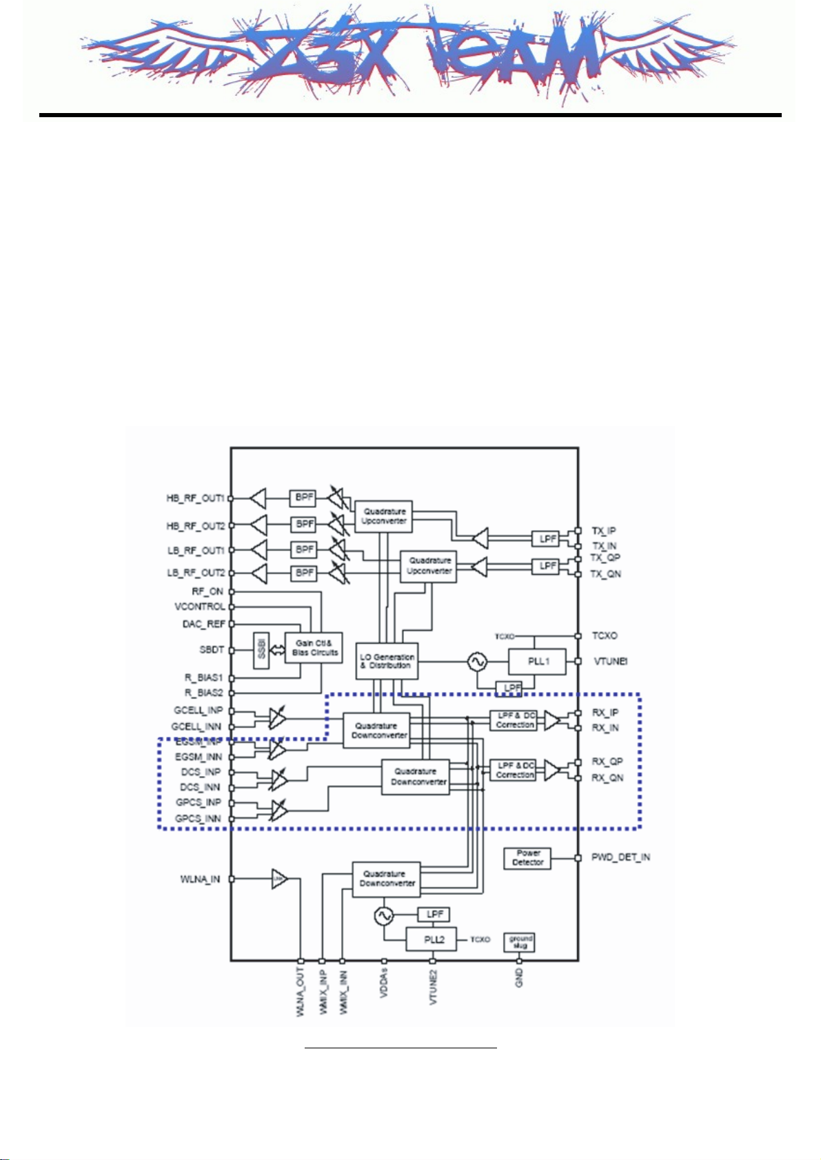
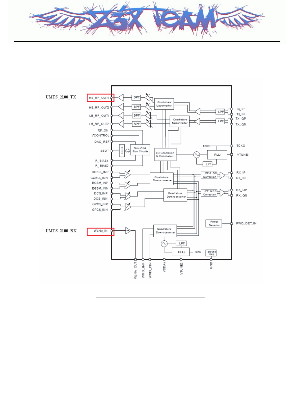
3.1 General Description
The HB620T supports UMTS-2100, EGSM-900, DCS-1800, and PCS-1900 based
GSM/GPRS/EDGE/UMTS. All receivers and the UMTS transmitter use the radioOne1Zero-IF
architecture to eliminate intermediate frequencies, directly converting signals between RF and
baseband. The quad-band GSM transmitters use a baseband-to-IF upconversion followed by an offset
phase-locked loop that translates the GMSK-modulated or 8-PSK-modulated signal to RF.
A generic, high-level functional block diagram of HB620T is shown in [Fig. 3.1]. One antenna collects
base station forward link signals and radiates handset reverse link signals. The antenna connects with
receive and transmit paths through a FEM(Front End Module).
The UMTS receive paths each include an LNA, an RF band-pass filter, and a downconverter that
translate the signal directly from RF-to-baseband using radio One ZIF techniques. The RFIC’s Rx
analog baseband outputs, for the receive chains, connect to the MSM IC. The UMTS and GSM Rx
baseband outputs share the same inputs to the MSM IC.
[Fig. 3.1] Block diagram of RF part
1
QUALCOMM’s branded chipset that implements a Zero-IF radio architecture.
Z3X-BOX.COM

LGE Internal Use Only
Copyright © 2008 LG Electronics. Inc. All right reserved.
Only for training and service purposes
3. TECHNICAL BRIEF
- 20 -
For the transmit chains, the RTR6275 IC directly translates the Tx baseband signals (from the MSM
device) to an RF signal using an internal LO generated by integrated on-chip PLL and VCO. The
RTR6275 IC outputs deliver fairly high-level RF signals that are first filtered by Tx SAWs and then
amplified by their respective UMTS PAs. The high- and low-band UMTS RF transmit signals emerge
from the RTR6275 transceiver.
In the GSM receive path, the received RF signals are applied through their band-pass filters and
down-converted directly to baseband in the RTR6275 transceiver IC. These baseband outputs are
shared with the UMTS receiver and routed to the MSM IC for further signal processing.
The GSM/EDGE transmit path employs one stage of up-conversion and, in order to improve efficiency,
is divided into phase and amplitude components to produce an open-loop Polar topology:
1. The on-chip quadrature upconverter translates the GMSK-modulated signal or 8-PSK modulated
signal, to a constant envelope phase signal at RF;
2. The amplitude-modulated (AM) component is applied to the ramping control pin of Polar power
amplifier from a DAC within the MSM
HB620T power supply voltages are managed and regulated by the PM6650 Power Management IC.
This versatile device integrates all wireless handset power management, general housekeeping, and
user interface support functions into a single mixed signal IC. It monitors and controls the external
power source and coordinates battery recharging while maintaining the handset supply voltages using
low dropout, programmable regulators.
The device’s general housekeeping functions include an ADC and analog multiplexer circuit for
monitoring on-chip voltage sources, charging status, and current flow, as well as user-defined off-chip
variables such as temperature, RF output power, and battery ID. Various oscillator, clock, and counter
circuits support IC and higher-level handset functions. Key parameters such as under-voltage lockout
and crystal oscillator signal presence are monitored to protect against detrimental conditions.
Z3X-BOX.COM
LGE Internal Use Only
Copyright © 2008 LG Electronics. Inc. All right reserved.
Only for training and service purposes
3. TECHNICAL BRIEF
- 21 -
3.2 GSM Mode
3.2.1 GSM Receiver
The Dual-mode HB620T’s receiver functions are operated by only one RFIC as follows:
■ EGSM-900, DCS-1800, PCS-1900 and UMTS-2100 modes use the RTR6275 IC only. Each mode
has independent front-end circuits and down-converters, but they share common baseband circuits
(with only one mode active at a time). All receiver control functions are beginning with SBI2controlled parameters.
RF Front end consists of antenna, antenna switch module (LSHS-M090UH) which includes three RX
saw filters (EGSM-900, DCS-1800 and PCS-1900). The antenna switch module allows multiple
operating bands and modes to share the same antenna. In HB620T, a common antenna connects to
one of six paths: 1) UMTS-2100 Rx/Tx, 2) EGSM-900 Rx, 3) EGSM-900 Tx, 4) DCS-1800 Rx, and 5)
DCS-1800, PCS-1900 Tx(High Band Tx’s share the same path), 6) PCS-1900 Rx. UMTS operation
requires simultaneous reception and transmission, so the UMTS Rx/Tx connection is routed to a
duplexer that separates receive and transmit signals. GSM900, DCS1800, and PCS1900 operation is
time division duplexed, so only the receiver or transmitter is active at any time and a frequency
duplexer is not required.
The GSM900, DCS1800, and PCS1900 receiver inputs of RTR6275 are connected directly to the
transceiver front-end circuits(filters and antenna switch module). GSM900, DCS1800, and PCS1900
receiver inputs use differential configurations to improve common-mode rejection and second-order
non-linearity performance. The balance between the complementary signals is critical and must be
maintained from the RF filter outputs all the way into the IC pins.
Since GSM900, DCS1800, and PCS1900 signals are time-division duplex (the handset can only
receive or transmit at one time), switches are used to separate Rx and Tx signals in place of frequency
duplexers - this is accomplished in the switch module.
2
The RFIC operating modes and circuit parameters are MSM-controlled through the proprietary 3- line Serial Bus Interface (SBI). The Application
Programming Interface (API) is used to implement SBI commands. The API is documented in AMSS Software - please see applicable AMSS
Software documentation for details.
ANT_SEL0 ANT_SEL1 ANT_SEL2
EGSM TX HIGH HIGH LOW
DCS/PCS TX HIGH LOW LOW
UMTS2100 HIGH LOW HIGH
EGSM RX LOW LOW/HIGH LOW
DCS RX LOW HIGH HIGH
[Table 3.1] Antenna Switch Module Control logic
Z3X-BOX.COM
LGE Internal Use Only
Copyright © 2008 LG Electronics. Inc. All right reserved.
Only for training and service purposes
3. TECHNICAL BRIEF
- 22 -
The GSM900, DCS1800, and PCS1900 receive signals are routed to the RTR6275 through band
selection filters and matching networks that transform single-ended 50Ω sources to differential
impedances optimized for gain and noise figure. The RTR input uses a differential configuration to
improve second-order inter-modulation and common mode rejection performance. The RTR6275 input
stages include MSM-controlled gain adjustments that maximize receiver dynamic range.
The amplifier outputs drive the RF ports of the quadrature RF-to-baseband downconverters. The
downconverted baseband outputs are multiplexed and routed to lowpass filters (one I and one Q)
having passband and stopband characteristics suitable for GMSK or 8-PSK processing. These filter
circuits include DC offset corrections. The filter outputs are buffered and passed on to the MSM6280 IC
for further processing.
[Fig. 3.2] RTR6275 RX feature
Z3X-BOX.COM
LGE Internal Use Only
Copyright © 2008 LG Electronics. Inc. All right reserved.
Only for training and service purposes
3. TECHNICAL BRIEF
- 23 -
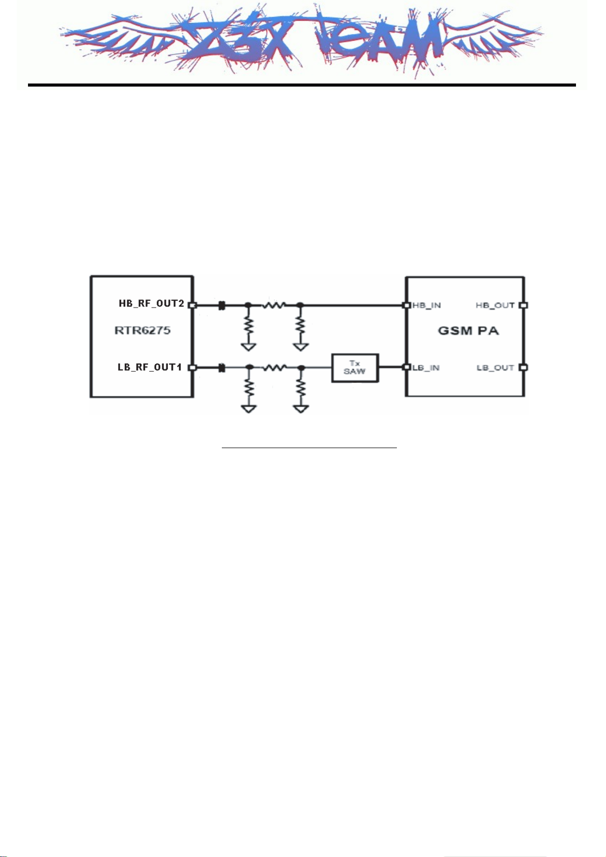
3.2.2 GSM Transmitter
The RTR6275 transmitter outputs (HB_RF_OUT2 and LB_RF_OUT1) include on-chip output matching
inductors. 50ohm output impedance is achieved by adding a series capacitor at the output pins. The
capacitor value may be optimized for specific applications and PCB characteristics based on passband
symmetry about the band center frequency. The suggested circuit is shown in [Fig. 3.3].
The RTR6275 IC is able to support EGSM900 and DCS1800/PCS1900 mode transmitting. This design
guideline shows a tri-band GSM application.
Both high-band and low band outputs are followed by resistive pads to ensure that the load Presented
to the outputs remains close to 50ohm. The low-band GSM Tx path also includes a Tx-band SAW filter
to remove noise-spurious components and noise that would be amplified by the PA and appear in the
GSM Rx band.
[Fig. 3.3] GSM Transmitter matching
Z3X-BOX.COM

LGE Internal Use Only
Copyright © 2008 LG Electronics. Inc. All right reserved.
Only for training and service purposes
3. TECHNICAL BRIEF
- 24 -
3.3 UMTS Mode
3.3.1 Receiver
The UMTS duplexer receiver output is routed to LNA circuits within the RTR6275 device. The UMTS Rx
input is provided with an on-chip LNA that amplifies the signal before a second stage filter that provides
differential downconverter. This second stage input is configured differentially to optimize second-order
intermodulation and common mode rejection performance. The gain of the UMTS frontend amplifier and
the UMTS second stage differential amplifier are adjustable, under MSM control, to extend the dynamic
range of the receivers. The second stage UMTS Rx amplifiers drive the RF ports of the quadrature RFto-baseband downconverters. The downconverted UMTS Rx baseband outputs are routed to lowpass
filters having passband and stopband characteristics suitable for UMTS Rx processing. These filter
circuits allow DC offset corrections, and their differential outputs are buffered to interface shared with
GSM Rx to the MSM IC. The UMTS baseband outputs are turned off when the RTR6275 is
downconverting GSM signals and on when the UMTS is operating.
3.3.2 Transmitter
The UMTS Tx path begins with differential baseband signals (I and Q) from the MSM device. These
analog input signals are amplified, filtered, and applied to the quadrature upconverter mixers. The
upconverter output is amplified by multiple variable gain stages that provide transmit AGC control. The
AGC output is filtered and applied to the driver amplifier; this output stage includes an integrated
matching inductor that simplifies the external matching network to a single series capacitor to achieve
the desired 50-Ω interface.
The RTR6275 UMTS output is routed to its power amplifier through a bandpass filter, and delivers fairly
high-level signals that are filtered and applied to the PA. Transmit power is delivered from the duplexer
to the antenna through the switch module.
The transceiver LO synthesizer is contained within the RTR6275 IC with the exception of the off-chip
loop filter components and the VC-TCXO. This provides a simplified design for multimode applications.
The PLL circuits include a reference divider, phase detector, charge pump, feedback divider, and digital
logic generator.
UMTS Tx using only PLL1, the LO generation and distribution circuits create the necessary LO signals
for nine different frequency converters. The UMTS transmitter also employs the ZIF architecture to
translate the signal directly from baseband to RF. This requires FLO to equal FRF, and the RTR6275 IC
design achieves this without allowing FVCO to equal FRF.
Z3X-BOX.COM
LGE Internal Use Only
Copyright © 2008 LG Electronics. Inc. All right reserved.
Only for training and service purposes
3. TECHNICAL BRIEF
- 25 -
[Fig. 3.4] RTR6275 IC functional block diagram
Z3X-BOX.COM

LGE Internal Use Only
Copyright © 2008 LG Electronics. Inc. All right reserved.
Only for training and service purposes
3. TECHNICAL BRIEF
- 26 -
3.4 LO generation and distribution circuits
The integrated LO generation and distribution circuits are driven by internal VCOs to support various
modes to yield highly flexible quadrature LO outputs that drive all GSM/EDGE and UMTS band
upconverters and downconverters; with the help of these LO generation and distribution circuits, true
zero-IF architecture is employed in all GSM and UMTS band receivers and transmitters to translate the
signal directly from RF to baseband and from baseband to RF.
Two fully functional fractional-N synthesizers, including VCOs and loop filters, are integrated within the
RTR6275 IC. The first synthesizer (PLL1) creates the transceiver LOs that support the UMTS 2100
transmitter, and all four GSM band receivers and transmitters including: GSM900, DCS1800, and
PCS1900. The second synthesizer (PLL2) provides the LO for the UMTS 2100 receiver. An external
TCXO input signal is required to provide the synthesizer frequency reference to which the PLL is
phase and frequency locked. The RTR6275 IC integrates most of PLL loop filter components on-chip
except two off-chip loop filter series capacitors, and significantly reduces off-chip component
requirement. With the integrated fractional-N PLL synthesizers, the RTR6275 has the advantages of
more flexible loop bandwidth control, fast lock time, and low-integrated phase error
Z3X-BOX.COM
LGE Internal Use Only
Copyright © 2008 LG Electronics. Inc. All right reserved.
Only for training and service purposes
3. TECHNICAL BRIEF
- 27 -
3.5 Off-chip RF Components
3.5.1 UMTS PAM (U105: ACPM-7381)
The UMTS PA output power is monitored by power detector circuits (U101 : RTR6275) .
This detector voltage can be used for transmitter calibration and monitor to meet RF system
specification.
3.5.2 VCTCXO (X101 : TG-5010LH(19.2M)-75A)
The Voltage Controlled Temperature Compensated Crystal Oscillator (VCTCXO) provides the reference
frequency for all RFIC synthesizers as well as clock generation functions within the MSM6280 IC. The
oscillator frequency is controlled by the MSM6280 ICs. TRK_LO_ADJ pulse density modulated signal in
the same manner as the transmit gain control TX_AGC_ADJ. A two-pole RC lowpass filter is
recommended on this control line.
The PM6650 IC controls the handset power-up sequence, including a special VCTCXO warm-up
interval before other circuits are turned on. This warm-up interval (as well as other TCXO controller
functions) is enabled by the MSM TCXO_EN line. The PM6650 IC VREG_TCXO regulated output
voltage is used to power the VCTCXO and is enabled before most other regulated outputs.
Any GSM mode power control circuits within the MSM6280 IC require a reference voltage for proper
operation and sufficient accuracy. Connecting the PM6650 IC REF_OUT directly to the MSM6275 IC
GSM_PA_PWR_CTL_REF provides this reference. This sensitive analog signal needs a 0.1 µF low
frequency filter near to MSM side, and isolate from digital logic and clock traces with ground on both
sides, plus ground above and below if routed on internal layers.
[Fig. 3.5] UMTS PAM, Duplexer, Coupler
3
ANT
4
ACMD-7602
PGND
FL104
1RX2
TX
+VPWR
C159
LDC151G9520Q-359
33p
SCDY0004101
R120
51
U104
2
1
IN
OUT
20dB
TER
COU
4
3
R121
120
1nHC162
C166
R119
51
8 dB
C167
1p
1p
PWR_DET
R122
120
C156
C158
C157
10u
100p
1u
U105ACPM-7381
11
PGND
110
VCC1
VCC2
2
9
GND3
RFIN
8
3
RFOUT
VMODE1
7
4
VMODE0
GND2
5
6
GND1
VEN
C169
100p
C160
10p
C163
C168
100p
DNI
PA_R1
PA_ON
4
5
O1
G3
1
IN
G1
2G23
FL105
EFCH1950TDF1
L125 3.9nH
C164
DNI
WCDMA_2100_TX_OUT
Z3X-BOX.COM
LGE Internal Use Only
Copyright © 2008 LG Electronics. Inc. All right reserved.
Only for training and service purposes
3.5.3 Front-End Module (FL101 : LSHS-M090UH)
This equipment uses a single antenna to support all handset operating modes, with an antenna switch
module select the operating frequency and band. UMTS operation requires simultaneous reception and
transmission, so the UMTS Rx/Tx connection is routed to a duplexer that separates receive and
transmit signals. The active connection is MSM-selected by three control lines (GPIO[9], GPIO[10], and
GPIO[11]). These GPIOs are programmed to be ANT_SEL0, ANT_SEL1, and ANT_SEL2 respectively.
3.5.4 PMIC Functional Block Diagram (U401 : PM6650-3P)
■ Input power management
- Valid external supply attachment and removal detection
- Supports unregulated (closed-loop) external charger supplies and USB supplies as input power
sources
- Supports lithium-ion main batteries
- Trickle, constant current, constant voltage, and pulsed charging of the main battery
- Supports coin cell backup battery (including charging)
- Battery voltage detectors with programmable thresholds
- VDD collapse protection
- Charger current regulation and real-time monitoring for over-current protection
- Charger transistor protection by power limit control
- Control drivers for two external pass transistors and one external battery MOSFET - MOSFET is
optional
- Voltage, current and power control loops
- Automated recovery from sudden momentary power loss
3. TECHNICAL BRIEF
- 28 -
ANT_SEL0 ANT_SEL1 ANT_SEL2
EGSM TX HIGH HIGH LOW
DCS/PCS TX HIGH LOW LOW
UMTS2100 HIGH LOW HIGH
EGSM RX LOW LOW/HIGH LOW
DCS RX LOW HIGH HIGH
[Table 3.2] Front End Module control logic
Z3X-BOX.COM

LGE Internal Use Only
Copyright © 2008 LG Electronics. Inc. All right reserved.
Only for training and service purposes
3. TECHNICAL BRIEF
- 29 -
■ Output voltage regulation
- One boost (step-up) switched-mode power supply (SMPS) for driving white LEDs and hosting
USBOTG
- Three buck (step-down) switched-mode power supplies that efficiently generate MSMC, MSME,
and PA (or second MSMC) supply voltages
- Supports dynamic voltage scaling (DVS) for MSMC and PA
- Eleven low dropout regulator circuits with programmable output voltages, implemented using three
different current ratings: 300 mA (two), 150 mA (six), and 50 mA (three). These can be used to
power MSMA, MSMP, RFRX1, RFRX2, RFTX, SYNT, TCXO, WLAN, MMC, USB, and RUIM
circuits.
- All regulators can be individually enabled/disabled for power savings
- Low power mode available on MSMA and MSMP regulators
- All regulated outputs are derived from a common bandgap reference - close tracking
■ Integrated handset-level housekeeping functions reduces external parts count, size, cost
- Analog multiplexer selects from 8 internal and up to 18 external inputs
- Multiplexer output’s offset and gain are adjusted, increasing the effective ADC resolution
- Adjusted multiplexer output is buffered and routed to an MSM device ADC
- Dual oscillators - 32.768 kHz off-chip crystal and on-chip RC assures MSM device sleep clock
- Crystal oscillator detector and automated switch-over upon lost oscillation
- Real time clock for tracking time and generating associated alarms
- On-chip adjustments minimize crystal oscillator frequency errors
- Circuits control TCXO warm-up and synchronize, deglitch, and buffer the TCXO signal
- TCXO buffer control for optimal QPH/catnap timing
- Three-stage over-temperature protection (smart thermal control)
■ Integrated handset-level user interfaces
- Four programmable current sinks recommended as keypad backlight, LCD backlight, camera
flash, and general-purpose drivers
- Vibration motor driver programmable from 1.2 to 3.1V in 100 mV increments
- Speaker driver with programmable gain, turn-on time, and muting; differential operation (drives
external 8 Ω speakers with volume controlled 500 mW)
Z3X-BOX.COM

LGE Internal Use Only
Copyright © 2008 LG Electronics. Inc. All right reserved.
Only for training and service purposes
3. TECHNICAL BRIEF
- 30 -
■ IC-level interfaces
- MSM device-compatible 3-line SBI for efficient initialization, status, and control
- Supports the MSM device’s interrupt processing with an internal interrupt manager
- Many functions monitored and reported through real-time and interrupt status signals
- Dedicated circuits for controlled power-on sequencing, including the MSM device’s reset signal
- Several events continuously monitored for triggering power-on/power-off sequences
- Supports and orchestrates soft resets
- USB-OTG transceiver for full-speed (12 Mb/s) and low speed (1.5 Mb/s) interfacing of the MSM
- device to computers as a USB peripheral, or connecting the MSM device to other peripherals
- RUIM level translators enable MSM device interfacing with external modules
■ Twelve multi-purpose pins that can be configured as digital or analog I/Os, bi-directional I/Os, or
current sinks. Default functions support the RUIM level translators, power-on circuits, analog
multiplexer inputs, an LED driver, and a reference voltage buffer.
■ Highly integrated functionality in a small package - 84-pin BCCS with a large center slug for
electrical ground, mechanical stability, and thermal relief.
Z3X-BOX.COM
LGE Internal Use Only
Copyright © 2008 LG Electronics. Inc. All right reserved.
Only for training and service purposes
3. TECHNICAL BRIEF
- 31 -
[Fig. 3.6] PM6650 Block Diagram
Z3X-BOX.COM

- 32 -
3. TECHNICAL BRIEF
LGE Internal Use Only
Copyright © 2008 LG Electronics. Inc. All right reserved.
Only for training and service purposes
3.5.5 GSM PAM (U102 : SKY77329)
The SKY77329 Power Amplifier Module (PAM) is designed in a compact form factor for quad-band
cellular handsets comprising GSM850/900, DCS1800, PCS1900, and supports Class 12 General
Packet Radio Service (GPRS) multi-slot operation.
The module consists of a GSM850/900 PA block and a DCS1800/PCS1900 PA block, impedance
matching circuitry for 50 Ω input and output impedances, and a Power Amplifier Control (PAC) block.
A custom CMOS integrated circuit provides the internal PAC function and interface circuitry. Two
separate Hetero-junction Bipolar Transistor (HBT) PA blocks are fabricated onto InGaP/GaAs die; one
supports the GSM850/900 bands, the other supports the DCS1800 and PCS1900 bands. Both PA
blocks share common power supply pins to distribute current. The GaAs die, the silicon die, and the
passive components are mounted on a multi-layer laminate substrate and the entire assembly is
encapsulated with plastic overmold.
[Fig. 3.7] GSM PAM Schematic
C127
C126
33u
1u
6
5
11
GND110GND2
VAPC
VBATT
2
DCS_PCS_IN
7
GSM_IN
1
TX_EN
3
BS
C139
15p
PGND1026PGND1127PGND12
PGND1
PGND2
PGND319PGND4
PGND5
PGND6
PGND7
PGND825PGND9
18
20
21
22
23
24
17
16
DCS_PCS_OUT
9
GSM_OUT
R107
2.2K
PGND20
36
C132
68p
13
14
15
4
GND3
GND4
GND5
RSVD18RSVD212RSVD3
U102
SKY77329
PGND1330PGND14
PGND15
PGND1633PGND17
PGND1834PGND19
28
29
31
32
35
GSM_PA_RAMP
C136
56p
C137
NA
C138
56p
C141
NA
+VPWR
R108
68
R109
91
GSM_PA_EN
GSM_PA_BAND
C140
15p
FL102
EFCH897MTDB1
DCS_PCS_TX
R110
91
5
4
G3
O1
1
IN
G12G2
3
R112
51
R114
120
GSM_TX
R115
120
Z3X-BOX.COM

- 33 -
3. TECHNICAL BRIEF
LGE Internal Use Only
Copyright © 2008 LG Electronics. Inc. All right reserved.
Only for training and service purposes
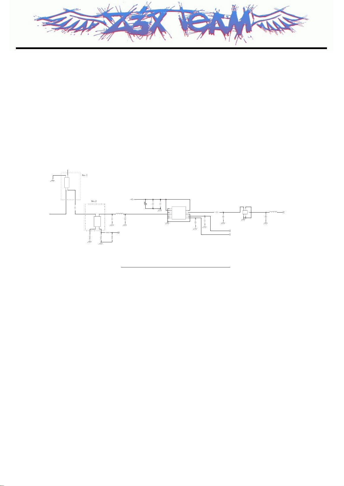
3.5.6 UMTS Duplexer(FL104: ACMD-7602)
A UMTS duplexer splits a single operating band into receive and transmit paths. Important
performance requirements include;
Insertion loss, this component is also in the receive and transmit paths ;
In the HB620T typical losses : UMTS2100_ Tx = 1.6 dB, UMTS2100_ Rx = 2.0 dB
Out-of-band rejection or attenuation, the duplexer provides input selectivity for the receiver, output
filtering for the transmitter, and isolation between the two. Rejection levels for both paths are specified
over a number of frequency ranges. Two Tx-to-Rx isolation levels are critical to receiver performance:
Rx-band isolation, the transmitter is specified for out-of-band noise falling into the Rx band. This noise
leaks from the transmit path into the receive path, and must be limited to avoid degrading receiver
sensitivity. The required Rx-band isolation depends on the PA out of-band noise levels and Rx-band
losses between the PA and LNA. Minimum duplexer Rx band isolation value is about 46.7 dB.
Tx-band isolation, the transmit channel power also leaks into the receiver. In this case, the leakage is
outside the receiver passband but at a relatively high level. It combines with Rx band jammers to
create cross-modulation products that fall in-band to desensitize the receiver. The required Tx-band
isolation depends on the PA channel power and Tx-band losses between the PA and LNA. Minimum
duplexer Tx-band isolation value is about 51.7dB.
Passband ripple, the loss of this fairly narrowband device is not flat across its passband. Passband
ripple increases the receive or transmit insertion loss at specific frequencies, creating performance
variations across the band.s channels, and should be controlled.
Return loss, minimize mismatch losses with typical return losses of 10 dB or more (VSWR <2:1).
Power handling, high power levels in the transmit path must be accommodated without degraded
performance. The specified level depends on the operating band class and mobile station class (per
the applicable standard), as well as circuit losses and antenna EIRP. Several duplexer characteristics
depend upon its source and load impedances. QUALCOMM strongly recommends an isolator be used
between the UMTS PA and duplexer to assure proper performance.
Z3X-BOX.COM

3.5.7 UMTS Rx RF filter (FL103 : EFCH2140TDE1)
An RF filter is located between the UMTS LNA and mixer. Insertion loss is important, but not as critical
as losses before the LNA. The most important parameters of this component include:
■ Out-of-band rejection or attenuation levels, usually specified to meet these conditions:
■ Far out-of-band signals - ranging from DC up to the first band of particular concern and from the last
band of particular concern to beyond three times the highest passband frequency.
■ Tx-band leakage - the transmitter channel power, although attenuated by the duplexer, still presents
a cross-modulation threat in combination with Rx-band jammers. The RF filter must provide rejection
of this Tx-band leakage
■ Other frequencies of particular concern . bands known to include other wireless transmitters that
may deliver significant power levels to the receiver input.
Parameter Frequency Our Prellminary spec. Unit
D/N: T2140F3A
Min. Typ. Max.
Passband 2110...2170 MHz
Insertion Ioss 2110...2170MHz 1.5 2.0 dB
Ripple in passband 2110...2170MHz 0.5 1.2 dB
Amplitude imbalance 2110...2170MHz -1.5 -1.11 +1.5\ dB
+0.73
Phase imbalance 2110...2170MHz -10.0 -1.92 +10.0 deg.
+1.02
Attenuation Att1 0.1...1980MHz 40 43 dB
Att2 1980...2040MHz 30 34 dB
Att3 2250...3000MHz 18 25 dB
Att4 3000...6000MHz 25 40 dB
VSWR Input 2110...2170MHz 1.5 2.0
Output 2110...2170MHz 1.5 2.0
Input impedance (Single Ended) 50 Ohm
Output impedance (Differential) 100//10nH Ohm
Maximum drive level 1920...1980MHz +10 mW
DC Input level +3 V
Operating temperature -25 +85 deg. C
Storage temperature -30 +85 deg. C
LGE Internal Use Only
Copyright © 2008 LG Electronics. Inc. All right reserved.
Only for training and service purposes
3. TECHNICAL BRIEF
- 34 -
[Table 3.3] UMTS Rx SAW Filter Specification
Z3X-BOX.COM

LGE Internal Use Only
Copyright © 2008 LG Electronics. Inc. All right reserved.
Only for training and service purposes
3. TECHNICAL BRIEF
- 35 -
3.5.8 Bluetooth (M701 : LBDA23QJS0)
The MSM6280 includes BT baseband embedded BT 1.1 compliant baseband core, so the other
bluetooth components are bluetooth RF module and Antenna. [Fig. 3.8] shows the bluetooth system
architecture in the HB620T.
[Fig. 3.8] Bluetooth system architecture
A
MSM 6280
Bluetooth Baseband
rt
BT_TX _RX_N
SBST
BT_DA TA
SBCK
SBDT
BT_CLK
7
TCXO
VREG _MSMP
VDD_
A
NT
LBRQ-2B43A
LBRQ-2B43A
SYNC_DET/ TX_EN
SYNC_DET/ TX_EN
RX_BB/TX _BB
RX_BB/TX _BB
16
BPF
GND Pa rt
GND
GND
1 2 3
678
1 2 3
678
BCM2004
15
15
LDO Pa rt
VDD_I NT
VDD_I NT
VCC_OUT
VCC_OUT
CLK_REF
CLK_REF
XTAL _IN
XTAL _IN
VDD _MSM
VDD _MSM
VDD_BA T
VDD_BA T
SBST
SBST
SBCK
SBCK
SBDT
SBDT
BlueQ Interfa ce Pa
5
5
4
4
13
13
11
11
12
12
Clo ck Part
9
9
Supply Pa rt
10
10
14
14
Z3X-BOX.COM

LGE Internal Use Only
Copyright © 2008 LG Electronics. Inc. All right reserved.
Only for training and service purposes
3. TECHNICAL BRIEF
- 36 -
3.5.9 DVB-H/T (U104 : DIB9080H)
■ DVB-H/T block diagram
DVB-H/T system block diagram is shown in the figure below. You can see the flow of DVB-H/T signal
by the below figure. First of all, you can see the antenna & the GSM rejection filter. The GSM rejection
filter is used to protect the DVB-H/T signal from the GSM interference which is near the DVB-H/T
signal band. First, DVB-H/T signal passes through the antenna and the GSM rejection filter. And the
tuner in DVB-H/T IC receives signal from the filter and passes the signal over to the demodulator
which demodulates the receiving signal and passes it to the DSP. DSP receives the signal from the
demodulator and decodes the signal, so that it can play sound with the speaker and display the video
of DVB-H/T signal through LCD. The DVB-H/T signal path is in the next page.
[Fig. 3.10] DVB-H/T Signal Path and Components(SUB)
[Fig. 3.9] DVB-H/T System Block Diagram
Z3X-BOX.COM

LGE Internal Use Only
Copyright © 2008 LG Electronics. Inc. All right reserved.
Only for training and service purposes
3. TECHNICAL BRIEF
- 37 -
■ GSM Rejection Filter (SUB FL101)
GSM rejection filter is placed between antenna and tuner. The filter is a type of BPF(Band Pass Filter)
and has pass-band from 470MHz to 862MHz. This filter is used protect DVB-H/T signal from GSM
interference which is near by DVB-H/T band. So, the performance of the filter is decided by attenuation
for GSM band.
■ Integrated Tuner in DVB-H/T IC (SUB U104)
Tuner is integrated in the IC. The functions of each of the individual blocks in the diagram will be
described in the following subsections.
[Fig. 3.11] DVB-H/T Signal Path and Components(MAIN)
Z3X-BOX.COM

- 38 -
3. TECHNICAL BRIEF
- RF switch
A RF switch allows the use of a single antenna input for all supported bands
- RXRF
RXRF consist of three parallel signal paths for different input bands, VHF, UHF and L-band.
Each path has an LNA, RFVGA and a WBD.
In UHF band, a notch filter improve the GSM compression up to 20dB. Depending on the sensitivity
loss, the DiB9080H can handle up to -15dBm GSM signal.
The function of the RFVGA is to amplify the signal after LNA while adding as little noise as possible.
It should be linear enough to handle all in-band interferes and GSM900 interferer.
The function of the WBD is to measure the amplitude on the output of RFVGA sio that the digital
baseband demodulator knows if or how far from compression RFVGA is.
- MIXER
The function of the MIXER is to down convert the signal from the radio frequency between 88MHz
and 1800MHz, to the baseband and performs channel selection. This is accomplished through the
selection of the LO frequency.
- Baseband
The baseband is a combination BBVGA and a high reject filter. The filter bandwidth is
programmable from 2 to 4 MHz. The gain is programmable in 0.13dB steps.
- LO
The PLL generates the LO I and Q signals needed for the down conversion.
- Crystal Oscillator
Crystal oscillator provides reference frequency for LO, DIGITAL and the system clock output for the
digital baseband demodulator.
- Bias
Bias block is based on a band gap voltage reference, voltage to current converter and a PTAT
current source for stable temperature behavior.
- ADC
This block samples the differential input analog signals. The maximum sampling frequency is
30MHz and the number of bits at both outputs of the ADC is 10.
LGE Internal Use Only
Copyright © 2008 LG Electronics. Inc. All right reserved.
Only for training and service purposes
Z3X-BOX.COM

- 39 -
3. TECHNICAL BRIEF
■ Integrated Demodulator in DVB-H/T IC (SUB U104)
The DiB9080H performs all the processing from RF input signal to MPEG-TS outout (in DVB-T mode)
and MPE tables/sections output (in DVB-H mode). The COFDM demodulator embedded in DiB9080H
uses the state of the art Signal Processing to offer high performance for mobile, portable and fixed
reception of Digital Terrestrial Television signals compliant with EN 300.744 DVB-T and ETS 301.192
DVB-H standards. The integrated tuner uses direct conversion technology for low power consumption.
Dual AGC BB/RF is implemented in order to offer very high dynamic range control through digital. A
digital filter with high rejection capability is added to cope with adjacent channels. Combined with the
interpolation function it allows the circuit to demodulate 8, 7 or 5 MHz channels without changing the
analog front-end.
Host Interface offering: SRAM like Interface
The roles of DIB9080H in the DVB-H/T front-end are below :
- Tuner : DiB9080H controls
RF frequency, RF Gain, Base band Gain, Switch on and off
Monitor the Wide Band Detector in order to avoid the saturation of first amplification stage of the
tuner
- Application processor :
Data transfer(MPE tables, sections), Monitoring and configuration
LGE Internal Use Only
Copyright © 2008 LG Electronics. Inc. All right reserved.
Only for training and service purposes
[Fig. 3.12] Integrated Tuner Block Diagram in DVB-H/T IC
Z3X-BOX.COM

- 40 -
3. TECHNICAL BRIEF
LGE Internal Use Only
Copyright © 2008 LG Electronics. Inc. All right reserved.
Only for training and service purposes
[Fig. 3.13] DiB9080H Functional Block Diagram
Z3X-BOX.COM

- 41 -
3. TECHNICAL BRIEF
■ DVB-H/T Interface
DVB-H/T interface block diagram is shown in below Figure. In the DVB-H/T system, DSP & MSM both
are related to control the demodulator. Each interface is shown in below figure. Each control signals
are explained in table
LGE Internal Use Only
Copyright © 2008 LG Electronics. Inc. All right reserved.
Only for training and service purposes
[Fig. 3.14] DVB-H/T Interface
[Table 3.4] DVB-H/T Interface
Name Note
OE Output Enable
CS Chip Select
WE Write Enable
DATA[0-7 ] DATA signal
ADDR[1-2 ] Address signal
RDY Ready signal
IRQ Interrupt signal
Z3X-BOX.COM

- 42 -
3. TECHNICAL BRIEF
■ Radio performance of DVB-H receiver
■ DVB-H/T Current Consumption
LGE Internal Use Only
Copyright © 2008 LG Electronics. Inc. All right reserved.
Only for training and service purposes
Item specification
Receive DVB-H (H3G) 470 ~ 750 MHz
Frequency DVB-H (TIM)
DVB-T 470 ~ 862 MHz
Reference DVB-H (H3G) -95.6 dBm for MFER 5%
BW : 7.61 MHz, Modulation : QPSK, Code rate : 1/2, Guard
interval : 1/8
DVB-H (TIM) -89.6 dBm for MFER 5%
BW : 7.61 MHz, Modulation : 16QAM, Code rate : 1/2,
Guard interval : 1/4
DVB-T -87.5 dBm [470 ~ 750MHz] for MFER 5%
-84.5 dBm [750 ~ 862MHz] for MFER 5%
BW : 7.61 MHz, Modulation : 16QAM, Code rate : 2/3,
Guard interval : 1/8
Maximum Input Level -10 dBm for MFER 5%
Frequency offset ± 350 KHz offset recovery
[Table 3.5] DVB-H/T RF performance
Stand by (BT Off condition) PLAY
DVB-H Same as Phone Deep Sleep state Average Under 300mA
DVB-T Same as Phone Deep Sleep state Average Under 400mA
Z3X-BOX.COM

- 43 -
3. TECHNICAL BRIEF
LGE Internal Use Only
Copyright © 2008 LG Electronics. Inc. All right reserved.
Only for training and service purposes
3.6 Digital Baseband (DBB/MSM6280)
3.6.1 General Description
A. Features (MSM6280)
■ Support for multimode operation - HSDPA, tri-band WCDMA(UMTS), quad GSM/GPRS/EDGE
■ Support for HSDPA downlink up to 7.2Mbps (initial commercial release will support 3.6Mbps
■ HSDPA. Later releases will have support for 7.2 Mbps HSDPA)
■ Support for WCDMA (UMTS) uplink data rate up to 384 kbps
■ High-performance ARM926EJ-S running at up to 225 MHz (later at 270 MHz for 7.2 Mbps HSDPA)
■ ARM Jazelle Java hardware acceleration for faster Java-based games and other applets
■ QDSP4000 high-performance DSP cores
■ Integrated Bluetooth 1.2 baseband processor for wireless connectivity to peripherals
■ Qcamera™ with 15 fps QVGA viewfinder resolution, and support for 4 MP camera sensors
■ Direct interface to digital camera module with video front end (VFE) image processing
■ True 3D graphics for advanced wireless gaming
■ SecureMSM v2.0 includes support for Open Mobile Alliance (OMA) DRM v2.0, SIM-lock and IMEI
integrity. Support for Q-fuse.
■ Audio on par with portable music players
■ Vocoder support (AMR, FR, EFR, HR)
■ Advanced 14 x 14 mm, 0.5 mm pitch, 409-pin lead-free CSP packaging technology
■ SD/SDIO hardware support
Z3X-BOX.COM

LGE Internal Use Only
Copyright © 2008 LG Electronics. Inc. All right reserved.
Only for training and service purposes
3. TECHNICAL BRIEF
- 44 -
[Fig. 3.15] Simplified Block Diagram of Baseband
Z3X-BOX.COM

LGE Internal Use Only
Copyright © 2008 LG Electronics. Inc. All right reserved.
Only for training and service purposes
3. TECHNICAL BRIEF
- 45 -
3.7 Subsystem(MSM6280)
3.7.1 ARM Microprocessor Subsystem
The MSM6280 device uses an embedded ARM926EJ-S microprocessor. This microprocessor,
through the system software, controls most of the functionality for the MSM, including control of the
external peripherals such as the keypad, LCD, SDRAM, and NAND-Flash devices. Through a
QUALCOMM proprietary serial bus interface (SBI) the ARM926EJ-S configures and controls the
functionality of the RTR6275 and PM6650 devices.
3.7.2 WCDMA R99 features
The MSM6280 device supports release 99 June 2004 of the W-CDMA FDD standard, including the
following features:
■ All modes and data rates for W-CDMA frequency division duplex (FDD), with the following
restrictions:
■ The downlink supports the following specifications:
- Up to four physical channels, including the broadcast channel (BCH), if present
- Up to three dedicated physical channels (DPCHs)
- Spreading factor (SF) range support from 4 to 256
- The following transmit diversity modes are supported:
Space time transmit diversity (STTD)
Time-switched transmit diversity (TSTD)
Closed-loop feedback transmit diversity (CLTD)
■ The uplink supports the following specifications:
■ The uplink provides the following UE support:
- One physical channel, eight TrCH, and 16 TrBks starting at any frame boundary
- A maximum data rate of 384 kbps
■ SMS (CS and PS)
■ Full SF range support from 4 to 256
■ PS data rate - 384 kbps DL / 384 kbps UL
■ CS data rate - 64 kbps DL / 64 kbps UL
■ AMR (all rates)
Z3X-BOX.COM

LGE Internal Use Only
Copyright © 2008 LG Electronics. Inc. All right reserved.
Only for training and service purposes
3. TECHNICAL BRIEF
- 46 -
3.7.3 HSDPA features
The MSM6280 device supports the HSDPA release 5 standard:
■ Supports HS-DSCH (HS-SCCH, HS-PDSCH and HS-DPCCH) in addition to the R99 transport
channels as defined in 3GPP specifications.
■ Supports a maximum of four simultaneous HS-SCCH channels as defined in 3GPP specifications.
■ Supports a maximum of 10 HS-PDSCH channels and supports both QPSK and 16 QAM modulation.
It supports UE category 6 in SW release 2.0 and category 8 in SW release 4.0.
■ Supports CQI, and ACK/NACK on HS-DPCCH channel as defined in 3GPP specifications.
■ Supports all incremental redundancy versions for HARQ, as defined in 3GPP specifications.
■ Can switch between HS-PDSCH and DPCH channel resources, as directed by the network.
■ Can be configured to support any of the two power classes 3 or 4 as defined in 3GPP R5
specifications (25.101).
■ Supports network activation of compressed mode by SF/2 or HLS on the DPCH for conducting interfrequency or inter-RAT measurements when the HS-DSCH is active.
■ Supports STTD on both associated DPCH and HS-DSCH simultaneously.
■ Supports CLTD mode 1 on the DPCH when the HS-PDSCH is active.
■ Supports STTD on HS-SCCH when either STTD or CLTD Mode 1 are configured on the associated
DPCH.
■ Supports TFC selection limitation on the UL factoring in the transmissions on the HS-DPCCH as
required in TS 25.133.
Z3X-BOX.COM

LGE Internal Use Only
Copyright © 2008 LG Electronics. Inc. All right reserved.
Only for training and service purposes
3. TECHNICAL BRIEF
- 47 -
3.7.4 GSM features
The following GSM modes and data rates are supported by the MSM6280 device hardware.
Support modes conform to release '99 specifications of the sub-feature.
■ Voice features
❏ FR
❏ EFR
❏ AMR
❏ HR
❏ A5/1, A5/2, and A5/3 ciphering
■ Circuit-switched data features
❏ 9.6k
❏ 14.4k
❏ Fax
❏ Transparent and non-transparent modes for CS data and fax
❏ No sub-rates are supported.
3.7.5 GPRS features
■ Packet switched data (GPRS)
❏ DTM (Simple Class A) operation
❏ Multi-slot class 12 data services
❏ CS schemes: CS1, CS2, CS3, and CS4
❏ GEA1, GEA2, and GEA3 ciphering
■ Maximum of four Rx timeslots per frame
3.7.6 EDGE features
■ EDGE E2 power class for 8 PSK
■ DTM (simple Class A), multi-slot class 12
■ Downlink coding schemes - CS 1-4, MCS 1-9
■ Uplink coding schemes - CS 1-4, MCS 1-9
■ BEP reporting
■ SRB loopback and test mode B
■ 8-bit, 11-bit RACH
■ PBCCH support
■ 1phase/2 phase access procedures
■ Link adaptation and IR
■ NACC, extended UL TBF.
Z3X-BOX.COM

LGE Internal Use Only
Copyright © 2008 LG Electronics. Inc. All right reserved.
Only for training and service purposes
3. TECHNICAL BRIEF
- 48 -
3.7.7 MSM6280 device audio processing features
■ Integrated wideband stereo CODEC
❏ 16-bit DAC with typical 88 dB dynamic range
❏ Supports sampling rates up to 48 kHz on the speaker path and 16 kHz on the microphone path
■ VR- Voice mail + voice memo
■ Acoustic echo cancellation
■ Audio AGC
■ Audio Codecs: AMR-NB, AAC, AAC Plus, Enhanced AAC Plus, Windows Audio v9, Real Audio 8
(G2)
■ Internal vocoder supporting AMR, FR, EFR, and HR
3.7.8 MSM6280 microprocessor subsystem
■ Industry standard ARM926EJ-S embedded microprocessor subsystem
❏ 16 kB instruction and 16 kB data cache
❏ Instruction set compatible with ARM7TDMI®
❏ ARM version 5TEJ instructions
❏ Higher performance 5 stage pipeline, Harvard cached architecture
❏ Higher internal CPU clock rate with on-chip cache
■ Java hardware acceleration
■ Enhanced memory support
Please note that NOR/PSRAM will not be supported on ESM6270.
❏ 75 MHz and 90 MHz bus clock for SDRAM
❏ 32-bit SDRAM
❏ Dual memory buses separating the high-speed memory subsystem (EBI1) from low-speed
❏ peripherals (EBI2) such as LCD panels
❏ 1.8 V or 2.6 V memory interface support (excluding EBI1)
❏ NAND FLASH memory interface
- 8/16-bit data I/O width NAND flash support
- 1- or 4-bit ECC
- 512-byte/2KB page-size support
- 2 chip selects supported for NAND Flash
❏ Boot from NAND
❏ Low-power SDRAM (LP-SDRAM) interface
■ Internal watchdog and sleep timers
Z3X-BOX.COM

LGE Internal Use Only
Copyright © 2008 LG Electronics. Inc. All right reserved.
Only for training and service purposes
3. TECHNICAL BRIEF
- 49 -
3.7.9 Supported interface features
■ USB On-the-Go core supports both slave and host functionality
■ Three universal asynchronous receiver transmitter (UART) serial ports
■ USIM controller (via UART)
■ Integrated 4-bit secure digital (SD) controller for SD and Mini SD cards
■ Parallel LCD interface
■ General-purpose I/O pins
■ External keypad interface
3.7.10 Supported multimedia features
■ Provide additional general purpose MIPS by using:
❏ Two QDSP4000s
❏ Dedicated hardware accelerators and compression engines
■ Improve Java, BREW, and game performance
❏ Integrated Java and 2D/3D graphics accelerator with Sprite engine
■ Enable various accessories via USB host connectivity.
❏ Integrated USB host controller functionality
■ Enable compelling visual and audio applications.
Qcamera
■ High-quality digital camera processing, supporting CCD or CMOS image sensors up to 4-megapixel
with 15 fps capture rate
■ 15 fps QVGA viewfinder
Qtv
■ Audio and video decoder that supports VOD, MOD and Broadcast multimedia services.
■ Audio Codecs supported: AMR-NB, AAC, AAC Plus, Enhanced AAC Plus, Windows®
■ Audio v9, RealAudio® v8
■ Integrated stereo wideband Codec for music/digital clips
■ CMX
■ Video Codecs supported: MPEG-4, H.263, H.264, Windows Media® v9 and RealNetworks® v10
Z3X-BOX.COM

LGE Internal Use Only
Copyright © 2008 LG Electronics. Inc. All right reserved.
Only for training and service purposes
3. TECHNICAL BRIEF
- 50 -
Video telephony services: Qvideophone
■ A two-way mobile video conferencing solution that delivers 15 fps @ QCIF
■ Video Codecs supported: MPEG-4 and H.263
■ Audio Codecs supported: AMR-NB.
Qcamcorder
■ Real time mobile video encoder
■ Video Codecs supported: MPEG-4, H.263.H.264
■ Audio Codecs supported: AMR-NB, AAC
■ Recording performance: 15 fps @ QVGA, 384 kbps
gpsOne
■ Integrated gpsOne processing
■ Standalone gpsOne mode in which the handset acts as a GPS receiver
CMX (MIDI and still image, animation, text, LED/vibrate support)
■ 72 simultaneous polyphonic tones
■ 44 kHz sampling rate
■ 512 kB wave table
■ Support of universal file formats
❏ Standard MIDI Format (SMF)
❏ SP-MIDI
❏ SMAF Audio playback (MA-2, MA-3, MA-5)
❏ XMF/OLS
❏ MFil (requires Docomo license)
■ PNG decoder
■ Pitch bend range support
■ LED/vibrate support
■ Scalable Vector Graphics (SVG- Tiny 1.1 + SVG Tiny 1.2)
■ MLZ decoder
■ Integrated PNG/SAF A.T.
Z3X-BOX.COM

LGE Internal Use Only
Copyright © 2008 LG Electronics. Inc. All right reserved.
Only for training and service purposes
3. TECHNICAL BRIEF
- 51 -
[Table 3.6] Summary of MSM6280 device features
Z3X-BOX.COM

LGE Internal Use Only
Copyright © 2008 LG Electronics. Inc. All right reserved.
Only for training and service purposes
3. TECHNICAL BRIEF
- 52 -
3.7.11 Serial Bus Interface(SBI)
The MSM6280 device’s SSBI is designed specifically to be a quick, low pin count control protocol for
QUALCOMM’s RTR6275 and PM6650 ASICs. Using the SSBI, the RTR6275 and PM6650 devices
can be configured for different operating modes and for minimum power consumption, extending
battery life in Standby mode. The SSBI also controls DC baseband offset errors.
3.7.12 Wideband CODEC
The MSM6280 device integrates a wideband voice/audio CODEC into the mobile station modem
(MSM). The CODEC supports two differential microphone inputs, one differential earphone output, one
single-ended earphone output, and a differential analog auxiliary interface.
The CODEC integrates the microphone and earphone amplifiers into the MSM6280 device, reducing
the external component count to just a few passive components. The microphone (Tx) audio path
consists of a two-stage amplifier with the gain of the second stage set interally. The Rx/Tx paths are
designed to meet the ITU-G.712 requirements for digital transmission systems.
3.7.13 Vocoder Subsystem
The MSM6280 device’s QDSP4000 supports AMR,FR,EFR and HR. In addition, the QDSP4000 has
modules to support the following audio functions: DTMF tone generation, DTMF tone detection, Tx/Rx
volume controls, Tx/Rx automatic gain control (AGC), Rx Automatic Volume Control(AVC), EarSeal
Echo Canceller (ESEC), Acoustic Echo Canceller (AEC), Noise Suppression(NS), and programmable,
13-tap, Type-I, FIR, Tx/Rx compensation filters. The MSM6280 device’s integrated ARM9TDMI
processor downloads the firmware into the QDSP4000 and configures QDSP4000 to support the
desired functionality.
3.7.14 ARM Microprocessor subsystem
The MSM6280 device uses an embedded ARM926EJ-S microprocessor. This microprocessor,
through the system software, controls most of the functionality for the MSM device, including control of
the external peripherals such as the keypad, LCD, RAM, ROM, and EEPROM devices. Through a
generic single serial bus interface (SSBI) the ARM926EJ-S configures and controls the functionality of
the RTR6275, and PM6650 devices.
3.7.15 Mode Select and JTAG Interfaces
The mode pins to the MSM6280 device determine the overall operating mode of the ASIC. The options
under the control of the mode inputs are Native mode, which is the normal subscriber unit operation,
ETM mode, which enables the built-in trace mode, and test mode for factory testing. The MSM6280
device meets the intent of the ANSI/IEEE 1149.1A-1993 feature list. The JTAG interface can be used
to test digital interconnects between devices within the mobile station during manufacture.
Z3X-BOX.COM

LGE Internal Use Only
Copyright © 2008 LG Electronics. Inc. All right reserved.
Only for training and service purposes
3. TECHNICAL BRIEF
- 53 -
3.7.16 General-Purpose Input/Output Interface
The MSM6280 device has general-purpose bidirectional input/output pins. Some of the GPIO pins
have alternate functions supported on them. The alternate functions include USB interface, additional
RAM, ROM, general-purpose chip selects, parallel LCD interface, and a UART interface. The function
of these pins is documented in the various software releases.
3.7.17. UART
The MSM6280 device employs three UARTs. UART1 has dedicated pins while UART2 and UART3
share multiplexed pins.
■ UART1 for data
■ UART2 (can be used for SIM interface)
■ UART3 for data
3.7.18. USB
The MSM6280 device integrates a universal serial bus (USB) controller that supports both
unidirectional and bidirectional transceiver interfaces. The USB controller acts as a USB peripheral
communicating with the USB host.
Z3X-BOX.COM

3.8 Power Block
3.8.1 General
MSM6280, included RF, is fully covered by PM6650(Qualcomm PMIC). PM6650 cover the power of
MSM6280, MSM memory, RF block, Bluetooth, USIM and TCXO.
Major power components are :
PM6650 : Phone power supply
MAX8645Y : LCD Backlight/Flash charge pump
3.8.2 PM6650
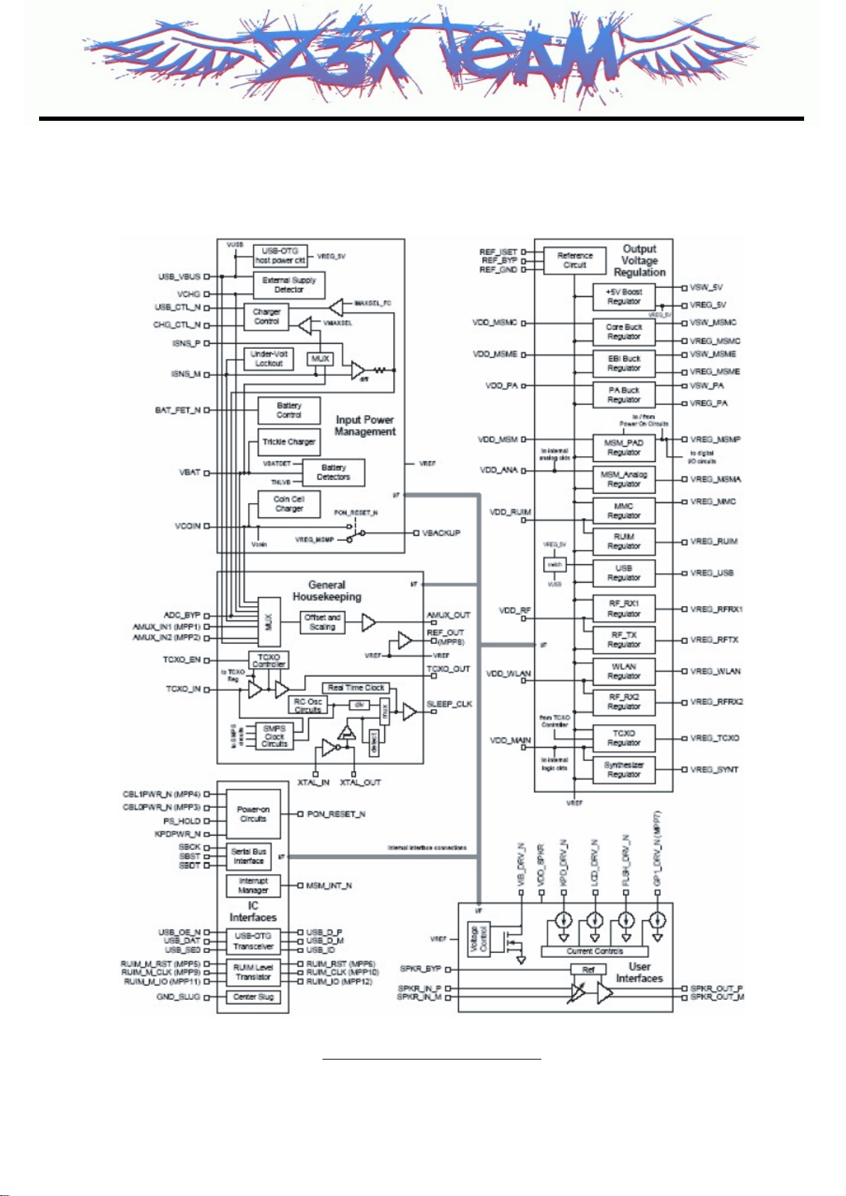
As shown in [Fig. 3.16], the PM6650 device integrates all wireless handset power management. The
power management portion accepts power from all the most common sources - battery, external
charger, adapter, coin cell back-up - and generates all the regulated voltages needed to power the
appropriate handset electronics. It monitors and controls the power sources, detecting which sources
are applied, verifying that they are within acceptable operational limits, and coordinates battery and
coin cell recharging while maintaining the handset electronics supply voltages. Eight programmable
output voltages are generated using low dropout voltage regulators, all derived from a common
trimmed voltage reference.
A dedicated controller manages the TCXO warm-up and signal buffering, and key
parameters(undervoltage lockout and crystal oscillator signal presence) are monitored to protect
against detrimental conditions. MSM device controls and statuses the PM6650 IC using Single Serial
Bus Interface (SSBI)supplemented by an Interrupt Manager for time-critical information. Another
dedicated IC Interface circuit monitors multiple trigger events and controls the power-on sequence.
LGE Internal Use Only
Copyright © 2008 LG Electronics. Inc. All right reserved.
Only for training and service purposes
3. TECHNICAL BRIEF
- 54 -
Z3X-BOX.COM

LGE Internal Use Only
Copyright © 2008 LG Electronics. Inc. All right reserved.
Only for training and service purposes
3. TECHNICAL BRIEF
- 55 -
[Fig. 3.16] PM6650 Functional Block Diagram
Z3X-BOX.COM

3.8.3 Charging control
A programmable charging block in PM6650 is used for battery charging. It is possible to set limits for
the charging current. The external supply typically connects directly to pin (VCHG). The voltage on this
pin (VCHG) is monitored by detection circuitry to ascertain whether a valid external supply is applied or
not. For additional accuracy or to capture variations over time, this voltage is routed internally to the
housekeeping ADC via the analog multiplexer. PM6650 circuits monitor voltages at VCHARGER and
ICHARGE pins to determine which supply should be used and when to switch between the two
supplies. These pins are connected to the Source (or emitter) and Drain (or collector) contacts of the
pass transistor respectively.
LGE Internal Use Only
Copyright © 2008 LG Electronics. Inc. All right reserved.
Only for training and service purposes
3. TECHNICAL BRIEF
- 56 -
KF700 Battery Bar Display(Stand By Condition)
Z3X-BOX.COM

LGE Internal Use Only
Copyright © 2008 LG Electronics. Inc. All right reserved.
Only for training and service purposes
3. TECHNICAL BRIEF
- 57 -
Trickle Charging
Trickle Charging of the main battery, enabled through SBI control and powered from VDD, is provided
by the PM6650 IC, The trickle charger is on-chip programmable current source that supplies current
from VDD to pin (VBAT). Trickle charging can be used for lithium-ion and nickel-based batteries, with
its performance specified below (3.2V). The charging current is set to 80mA.
Parameter Min Typ Max Unit
Trickle Current 60 80 100 mA
Z3X-BOX.COM

LGE Internal Use Only
Copyright © 2008 LG Electronics. Inc. All right reserved.
Only for training and service purposes
Constant Current Charging
The PM6650 IC supports constant current charging of the main battery by controlling the charger pass
transistor and the battery transistor. The constant current charging continues until the battery reaches
its target voltage, 4.2V.
Constant Voltage Charging
Constant voltage charging begins when the battery voltage reaches a target voltage, 4.2V. The end of
constant voltage charging is commonly detected 10% of the full charging current.
■ Charging Method : CC & CV (Constant Current & Constant Voltage)
■ Maximum Charging Voltage : 4.2V
■ Maximum Charging Current : 600mA
■ Nominal Battery Capacity : 900mAh
■ Charger Voltage : 5.1V
■ Charging time : Max 3h (Except time trickle charging)
■ Full charge indication current (icon stop current) : 193mA
■ Low battery POP UP : Idle - 3.56V, Dedicated(GSM/WCDMA) - 3.56V
■ Low battery alarm interval : Idle - 3 min, Dedicated - 1min
■ Cut-off voltage : 3.20V
3. TECHNICAL BRIEF
- 58 -
Z3X-BOX.COM

3.9 External memory interface
The MSM6280 device was designed to provide two distinct memory interfaces. EBI1 was targetedv for
supporting high speed synchronous memory devices. EBI2 was targeted towards supporting slower
asynchronous devices such as LCD, NAND flash, SRAM, etc. In addition, MSM6280 provide SD bus
interface. HB620T supports 512MByte free user memory using SD interface.
❏ EBI1 Features
- 16 bit static and dynamic memory interface
- 32 bit dynamic memory interface
- 24 bits of address for static memory devices which can support up to 32MBytes on each chip
select
- Synchronous burst memories supported (burst NOR, burst PSRAM)
- Synchronous DRAM memories supported
- Byte addressable memory supporting 8 bit, 16 bit and 32 bit accesses
- Pseudo SRAM (PSRAM) memory support
❏ EBI2 Features
- Support for asynchronous FLASH and SRAM(16bit & 8bit).
- Interface support for byte addressable 16bit devices (UB_N & LB_N signals).
- 2Mbytes of memory per chip select.
- Support for 8 bit/16bit wide NAND flash.
- Support for parallel LCD interfaces, port mapped of memory mapped(18 or 16 bit).
❏ 2Gb NAND(16bit, Large Block ) flash memory + 1Gb SDRAM (32bit)
❏ 1-CS(Chip Select) are used.
❏ The SD bus allows the dynamic configuration of the number of data line from 1 to 4 Bidirectional
data signal. After power up by default, the Device will use only DAT0. After initialization, host can
change the bus width.
LGE Internal Use Only
Copyright © 2008 LG Electronics. Inc. All right reserved.
Only for training and service purposes
3. TECHNICAL BRIEF
- 59 -
Interface Spec
Device Part Name Maker Read Access Time
FLASH TYA000BC00DOGG Toshiba 35 ns
SDRAM TYA000BC00DOGG Toshiba 8 ns
[Table 3.7] External memory interface
Z3X-BOX.COM

LGE Internal Use Only
Copyright © 2008 LG Electronics. Inc. All right reserved.
Only for training and service purposes
3. TECHNICAL BRIEF
- 60 -
[Fig. 3.17] Simplified Block Diagram of Memory Interface
Z3X-BOX.COM

3.10 H/W Sub System
3.10.1 RF Interface
A. RTR6275 (WCDMA Tx, GSM Tx/Rx)
MSM6280 controls RF part(RTR6275) using these signals.
❏ SBST : SSBI I/F signals for control Sub-chipset
❏ PA_ON1 : Power AMP on RF part
❏ RX0_I/Q_M/P,TX_I/Q_M/P : I/Q for T/Rx of RF
❏ TX_AGC_ADJ : control the gain of the Tx signal prior to the power amplifier
❏ DAC_REF : Reference input to the MSM Tx data DACs
LGE Internal Use Only
Copyright © 2008 LG Electronics. Inc. All right reserved.
Only for training and service purposes
3. TECHNICAL BRIEF
- 61 -
[Fig. 3.18] Schematic of RF Interface of MSM6280
SBDT1_GPIO1
GPIO28
GPIO43
GPIO66
TX_AGC_ADJ
TRK_LO_ADJ
PA_ON0
Q_OUT_N
Q_OUT
I_OUT_N
I_OUT
DAC_REF
Q_IM_CH1
Q_IP_CH1
I_IM_CH1
I_IP_CH1
Q_IM_CH0
Q_IP_CH0
I_IM_CH0
I_IP_CH0
TRST_N
RTCK
MDDIC_DATP
MDDIC_DATN
MDDIC_STBP
MDDIC_STBN
H25
F26
H11
D5
J21
A6
N19
W15
AA15
AE13
H9
B6
F8
AA1
Y6
L25
H6
F18
H18
H13
L13
F19
F17
A12
B12
A13
B13
F12
W23
V23
V25
W25
AA25
Y25
AB25
AC25
D17
H17
H15
D16
TCK
F15
TMS
D15
TDI
A17
TDO
H16
K19
N21
G4
J8
H12
B4
T23
T19
D11
H10
F10
D9
A8
B8
G23
F23
E26
E25
H21
R19
A22
A23
B22
B23
TP202
TCC_PWR_EN
CAM_SYSCLK
LCD_IF_MODE_0
V_CAM_RESET_N
EAR_SENSE_N
FOLDER_DETECT
RMT_INT
RCV_EN
TCC_RESET_N
LCD_MAKER_ID
TCXO_EN
PA_ON
(WCMDA 2100 PAM Enable)
TX_QM
TX_QP
TX_IM
TX_IP
DAC_REF
RX_QM
RX_QP
RX_IM
RX_IP
JTAG_TRST_N
JTAG_TCK
JTAG_TMS
JTAG_TDI
JTAG_TDO
JTAG_RTCK
LCD_RESET_N
VC_IO_OFF
TCC_INT
M_CAM_RESET_N
TX_ON
ANT_SEL2
ANT_SEL1
ANT_SEL0
BT_CLK
BT_SBST
BT_SBCK
BT_SBDT
BT_TX_RX_N
BT_DATA
R211 2K
R212
100K
C226
33nF
TX_AGC_ADJ
TRK_LO_ADJ
PA_R1
GSM_PA_BAND
GSM_PA_EN
WDOG_STB_SBCK1_GPIO0
PA_ON1_GPIO2
GRFC9_GPIO12
CAMCLK_PO_GP_MN_GPIO13
USB_RX_DATA_GPIO29
XMEM2_CS_N2_GPIO35
XMEM2_CS_N3_GPIO36
LCD_EN_GPIO37
SYNTH2_GPIO65
XMEM1_CS_N3_SDRAM1_CS_N1_GPIO77
XMEM1_CS_N1_GPIO76
UART3_RFR_N_GPIO87
UART2_DP_RX_DATA_GPIO89
SYNTH0_GP_PDM0_GPIO92
SBST1_GPIO93
TCXO_EN_GPIO94
GP_PDM2_PA_RAN_GE1
GP_PDM1_PA_RAN_GE0
Z3X-BOX.COM
AUX_PCM_CLK_GRFC14_GPIO80
AUX_PCM_DIN_GRFC13_GPIO14
AUX_PCM_DOUT_GRFC12_GPIO103
AUX_PCM_SYNC_GRFC11_GPIO102
TX_ON_GRFC10
GRFC8_GPIO11
GRFC7_GPIO10
GRFX6_GPIO9
GRFC5_AUX_SBST_GPIO8
GRFC4_AUX_SBCK_GPIO7
GRFC3_GPIO6
GRFC2_GPIO5
GRFC1_AUX_SBDT_GPIO4
GRFC0_GPIO3
BT_CLK_GPIO25
BT_SBST_GPIO24
BT_SBCK_GPIO23
BT_SBDT_GPIO22
BT_TX_RX_N_GPIO21
BT_DATA_GPIO20

LGE Internal Use Only
Copyright © 2008 LG Electronics. Inc. All right reserved.
Only for training and service purposes
B. the others
❏ TRK_LO_ADJ : TCXO(19.2M) Control
❏ PA_ON : WCDMA(2100) TX Power Amp Enable
❏ ANT_SEL[0-2] : Ant Switch Module Mode Selection(WCDMA,GSM Tx/Rx, DCS-PCS Tx/Rx)
❏ GSM_PA_BAND : GSM/DCS-PCS Band Selection of Power Amp
❏ GSM_PA_RAMP : Power Amp Gain Control of APC_IC
❏ GSM_PA_EN : Power Amp Gain Control Enable of APC_IC
3.10.2 MSM Sub System
SIM Interface
SIM interface scheme is shown in [Fig. 3.19].
And, there control signals are followed
❏ USIM_CLK : USIM Clock
❏ USIM_Reset : USIM Reset
❏ USIM_Data : USIM Data T/Rx
UART Interface
UART signals are connected to MSM GPIO through IO connector with 115200 bps speed.
3. TECHNICAL BRIEF
- 62 -
[Fig. 3.14] SIM Interface
GPIO_Map Name Note
GPIO_96 UART_RXD Data_Rx
GPIO_95 UART_TXD Data_Tx
[Table 3.8] UART Interface
Z3X-BOX.COM

USB
The MSM6280 device contains a Universal Serial Bus (USB) interface to provide an efficient
interconnect between the mobile phone and a personal computer (PC). The USB interface of the
MSM6280 was designed to comply with the definition of a peripheral as specified in USB Specification,
Revision 2.0. Therefore, by definition, the USB interface is also compliant as a peripheral with the USB
Specification, Revision 2.0. The USB Specification Revision 2.0 defines three speeds of operation,
namely low-speed (1.5 Mbps) and full-speed (12 Mbps), and hi-speed(480Mbps). HB620T supports
low-speed and full-speed.
LGE Internal Use Only
Copyright © 2008 LG Electronics. Inc. All right reserved.
Only for training and service purposes
3. TECHNICAL BRIEF
- 63 -
[Table 3.9] USB Signal Interface
Name Note
USB_DAT Data to/from MSM
USB_SE0 Data to/from MSM
USB_OE_N Out-Put Enable of Transceiver
USB_VBUS USB_Power From Host(PC)
USB_D+ USB Data+ to Host
USB_D- USB Data- to Host
[Fig. 3.20] Schematic of USB block(MSM6280 Side & PM6650 Side)
USB_DAT_VP
USB_OE_TP_N
GPIO40
GPIO42
D6
D7
PS_HOLD
PM_INT_N
USB_SE0_VM
N23
N26
USB_SE0
USB_DAT
MMC_DATA_SDCC_DAT0_GPIO32
MMC_CLK_SDCC_CLK_GPIO31
MMC_CMD_GPIO30
Z3X-BOX.COM
L14
N25
H14
M16
USB_OE_N
MICROSD_CLK
MICROSD_CMD
MICROSD_DATA(0)
USB_VBUS
C424
4.7u
R409
47K
USB_CTL_N
USB_DAT
USB_D+
USB_SE0
USB_D-
USB_OE_N
11
USB_ID
12
VREG_5V
13
USB_OE_N
14
VSW_5V
15
USB_CTL_N
16
USB_VBUS
17
USB_DAT
18
USB_D_P
19
USB_SE0
20
USB_D_M
21
GP1_DRV_N(MPP7)

- 64 -
3. TECHNICAL BRIEF
LGE Internal Use Only
Copyright © 2008 LG Electronics. Inc. All right reserved.
Only for training and service purposes
3.10.3 HKADC(House Keeping ADC)
The MSM6280 device has an on-chip 8-bit analog-to-digital converter (HKADC) which is tended to
digitize DC signals corresponding to analog parameters such as battery voltage, temperature, and RF
power levels. The MSM6280 device has six analog input pins which are multiplexed to the input of the
internal HKADC.
[Fig. 3.21] MSM6280HKADC Block diagram
[Table 3.10] HKADC channel table
Channel Signal Note
HKADC0 AMUX_OUT RF PAM Temperature Check
HKADC1 VBATT_SENSE Battery voltage level
HKADC2 EAR_MIC_P Ear jack Detection
HKADC3 RNT_ADC Headset remote key detection
HKADC4 PCB_Rev_ADC PCB Version Check
HKADC5 Battery_THERM Battery Temperature Check
Z3X-BOX.COM

- 65 -
3. TECHNICAL BRIEF
LGE Internal Use Only
Copyright © 2008 LG Electronics. Inc. All right reserved.
Only for training and service purposes
3.10.4 Key Pad
There are 29 key buttons. Shows the Key Matrix & Keypad circuit. ‘END’ Key is connected to
PMIC(PM6650).
[Table 3.11] Key Matrix Mapping Table
COL(0) COL(1) COL(2) COL(3) COL(4) COL(5)
ROW 0 SEND 1 4 7 * SIDE1
ROW 1 SOET1 2 5 8 0 SIDE2
ROW 2 UP 3 6 9 # SIDE3
ROW 3 SOET2 TV Guide MYch MENU HOOK
ROW 4 LEFT OK RIGHT CLR DOWN
[Fig. 3.22] Main Keypad Circuit
KEY_ROW[0]
KEY_ROW[1]
KEY_ROW[2]
KEY_ROW[3]
KEY_ROW[4]
KEY_COL[0]
KEY_COL[1]
KEY_COL[2]
KEY_COL[3]
KEY_COL[4]
VREG_MSMP_2.7V
51KR504
51KR503
CN503
1
2
CN504
3
4
3
2
1
R506 51K
R505 51K
R507 51K
HOT501 star
(VT CALL)
HOT502
(JAVA)
HOT503
(MENU)
501
504
HOT507HOT506 HOT508
502
509508
503
506505
510
HOT509
507
sharp
HOT505HOT504
HOT510
Z3X-BOX.COM
100ohm
R904
100ohm
R905
100ohm
R906
VA710 EVLC14S02050
100ohm
R907
100ohm
R908
VA714 EVLC14S02050
VA711 EVLC14S02050
VA712 EVLC14S02050
EVLC14S02050
VA713
KEY_ROW[0]
KEY_ROW[1]
KEY_COL[5]
KEY_ROW[2]
KEY_COL[5]
SIDE_VOLUME_UP_KEY
SIDE_VOLUME_DOWN_KEY
SIDE_VOLUME_CAMERA
SIDE KEY
KEY MATRIX

3.10.5 Camera Interface
HB620T Installed a 2M and VGA Camera. Below [Fig. 3.23] shows the camera board to board
connector and camera I/F signal.
The MEGA Camera module is connected to LCD FPCB with 24pin Board to Board connector. Its
interface is dedicated camera interface port in MSM6280. The MEGA camera port supply 24.576MHz\
master clock to camera module, vertical sync signal, horizontal sync signal, reset signal and 8bits data
from camera module. The MEGA camera module is controlled by I2C port from MSM6280.
LGE Internal Use Only
Copyright © 2008 LG Electronics. Inc. All right reserved.
Only for training and service purposes
3. TECHNICAL BRIEF
- 66 -
[Fig. 3.23] Camera PCB Board to Board Connector
VREG_CAM_AVDD_2.9V
VREG_CAM_DVDD_2.8V
VREG_CAM_DVDD_1.5V
CN104
G1 G2
1
24
2
CAM_DATA[7]F
CAM_DATA[6]F
CAM_DATA[5]F
CAM_DATA[4]F
CAM_DATA[3]F
CAM_DATA[2]F
CAM_DATA[1]F
CAM_DATA[0]F
M_CAM_RESET_N
MC_IO_OFF
EVLC14S02050VA110
3
4
5
6
7
8
9
10
11
12
G3 G4
23
22
21
20
19
18
17
16
15
14
13
1uC952
1uC111
I2C_SCL
I2C_SDA
CAM_VSYNC
CAM_HSYNC
CAM_SYSCLK
VREG_CAM_AVDD_2.9V
VCAM_1.8V
AXK720147G
CN105
20
VC_IO_OFF
CAM_SYSCLK
CAM_PCLK
CAM_DATA[0]F
CAM_DATA[1]F
CAM_DATA[2]F
CAM_DATA[3]F
CAM_DATA[4]F
CAM_DATA[5]F
Z3X-BOX.COM
1
192
18
3
17
4
16
5
15
6
14
7
13
8
12
9
11
10
I2C_SCL
I2C_SDA
CAM_HSYNC
CAM_VSYNC
CAM_DATA[7]F
CAM_DATA[6]F
V_CAM_RESET_N
VA109
EVLC14S02050

I/O pin description
LGE Internal Use Only
Copyright © 2008 LG Electronics. Inc. All right reserved.
Only for training and service purposes
3. TECHNICAL BRIEF
- 67 -
No Pin Name I/O Description
1 AGND G Analog GND
2D7ODigital Video data [7]
3D6ODigital Video data [6]
4D5ODigital Video data [5]
5D4ODigital Video data [4]
6D3ODigital Video data [3]
7D2ODigital Video data [2]
8D1ODigital Video data [1]
9D0ODigital Video data [0]
10 PCLK O Clock for output data
11 RESETB I RESET (Active Low)
12 STDBYB I Stand BY (Active Low)
13 DGND G GND
14 DVDD-CORE I 1.5V, Core Digital Power
15 IOVDD I 1.8V or 2.8V, I/O Digital Power
16 AVDD I 2.8V, Analog Power
17 DGND G Digital GND
18 MCLK I Master input clock
19 HSYNC O Horizontal Sync Signal
20 VSSYNC O Vertical Sync Signal
21 DGND G Digital GND
22 SDA I/O I2C Data
23 SCK I/O I2C Clock
24 AGND I Analog GND
[Table 3.12] Interface between MEGA Camera Module and MAIN PCB (in camera module)
Z3X-BOX.COM

LGE Internal Use Only
Copyright © 2008 LG Electronics. Inc. All right reserved.
Only for training and service purposes
3. TECHNICAL BRIEF
- 68 -
The VGA Camera module is connected to LCD FPCB with 20pin Board to Board connector
(AXK720147G). Its interface is dedicated camera interface port in MSM6280. The VGA camera port
supply 24.576MHz master clock to camera module and receive 24.576MHz pixel clock (30fps), vertical
sync signal, horizontal sync signal, reset signal and 8bits data from camera module. The VGA camera
module is controlled by I2C port from MSM6280.
I/O Infomationa
No Name Type Description
1 ENABLE I Active ‘High’
2 MCLK I Master Clock
3 GND I Ground
4 PCLK O Video Output Clock D [0:7]
5D0OImaga Data [0]
6D1OImaga Data [1]
7D2OImaga Data [2]
8D3OImaga Data [3]
9D4OImaga Data [4]
10 D5 O Imaga Data [5]
11 D6 O Imaga Data [6]
12 D7 O Imaga Data [7]
13 VSYNC I Vertical Synchronization
14 HSYNC I Horizontal Synchronization
15 GND I Ground
16 SDA I/O Data for two wire serial interface
17 SCL I Clock for two wire serial interface
18 RESET I Reset initializes sensor Active Low
19 DVDD I Digital core circuit power supply voltage
20 AVDD &IOVDD I Analog core circuit power supply voltage &
Digital I/O circuit power supply voltage
[Table 3.13] Interface between VGA Camera Module and FPCB (in camera module)
Z3X-BOX.COM

3.10.6 LCD Module (IM300SBN1A : LG Innotek)
- The IM200RST1A model is a Color Landscape TFT(Main) & Color TFT(Sub) LCD supplied by LG
Innotek. This main Module has a 2.0 inch diagonally measured active display area with
320(RGB)X240 resolution and sub Module has a 0.86 inch diagonally measured active display area
with 34(RGB)X96 resolution. each pixel is divided into Red, Green and Blue subpixels and dots which
are arranged in vertical stripes.
* Features
- Display mode : Main: Normally Black, Transmissive LCD. VA mode 262K colors
Sub: Normally White, Trasmissive LCD, VA mode 65K colors
- LCD Driver IC- Main : R61513 (RENESAS) Sub : NT39107(Novatek)
- Driving Method : a-Si TFT Active Matrix
- 16/18 Bit, CPU I/F Parallel
LGE Internal Use Only
Copyright © 2008 LG Electronics. Inc. All right reserved.
Only for training and service purposes
3. TECHNICAL BRIEF
- 69 -
[Fig. 3.24] LCD Module Block Diagram
Z3X-BOX.COM

- 70 -
3. TECHNICAL BRIEF
3.10.7 Display
LCD module is connected to LCD F-PCB with 40 pin B TO B connector.
The LCD module is controlled by 16/18-bit EBI2 in MSM6280.
Audio Signal Processing & Interface
Audio signal processing is divided uplink path and downlink path. The uplink path amplifies the audio
signal from MIC and converts this analog signal to digital signal and then transmits it to DBB Chip
(MSM6280). This transmitted signal is reformed to fit in GSM & WCDMA frame format and delivered to
RF Chipset. The downlink path amplifies the signal from DBB chip (MSM6280) and outputs it to
receiver (or speaker).
The receive path can be directed to either one of two earphone amplifiers or the auxiliary output. The
outputs earphone1 (EAR1OP, EAR1ON) and auxiliary out (LINE_OP, LINE_ON) are differential
outputs. Earphone2 (HPH_L, HPH_R) is a single-ended output stage designed to drive a headset
speaker. The microphone interface consists of two differential microphone inputs, one differential
auxiliary input and a two-stage audio amplifier.
LGE Internal Use Only
Copyright © 2008 LG Electronics. Inc. All right reserved.
Only for training and service purposes
TCC_2.7V_EHI_LCD
CN103
G2
MAIN_LED1
MAIN_LED4
WLED_PWR
FILTER_LCD_RESET_N
FILTER_MM_LCD_DATA[15]
FILTER_MM_LCD_DATA[13]
FILTER_MM_LCD_DATA[11]
FILTER_MM_LCD_DATA[9]
FILTER_MM_LCD_DATA[7]
FILTER_MM_LCD_DATA[5]
FILTER_MM_LCD_DATA[3]
FILTER_MM_LCD_DATA[1]
MM_LCD_RD_N
FILTER_MM_LCD_ADS_N
MM_LCD_VSYNC
20 21
19
18
17
16
15
14
13
12
11
10
9
8
7
6
5
4
3
2
1
G1
AXK8L40125G
ENBY0020201
22
23
24
25
26
27
28
29
30
31
32
33
34
35
36
37
38
39
40
MAIN_LED2
MAIN_LED3
MAIN_LED5
LCD_IF_MODE_0
FILTER_MM_SUB_LCD_CS_N
FILTER_MM_LCD_WE_N
MM_MAIN_LCD_CS_N
LCD_MAKER_ID
FILTER_MM_LCD_DATA[14]
FILTER_MM_LCD_DATA[12]
FILTER_MM_LCD_DATA[10]
FILTER_MM_LCD_DATA[8]
FILTER_MM_LCD_DATA[6]
FILTER_MM_LCD_DATA[4]
FILTER_MM_LCD_DATA[2]
FILTER_MM_LCD_DATA[0]
C409 0.1u
D402
PLW0501H-LF
INSTPAR
Z3X-BOX.COM

- 71 -
3. TECHNICAL BRIEF
LGE Internal Use Only
Copyright © 2008 LG Electronics. Inc. All right reserved.
Only for training and service purposes
# Image Signal Processor Chip
[Fig. 3.25] Audio Interface Detailed Diagram(MSM6280)
Z3X-BOX.COM

- 72 -
3. TECHNICAL BRIEF
3.11 Feature List
3.11.1 USB Interface
* The MSM6280 device integrates a universal serial bus (USB) controller that supports both
unidirectional and bidirectional transceiver interfaces characteristics:
■ Compliant with both the USB 2.0 Specification and the OTG Supplement
■ Complies with 3-wire USB support only
■ USB Transceiver integrated in PM6650-3P power management device
■ Either low-speed (1.5Mbps) or full-speed (12Mbps) as a host
■ In peripheral mode, PM6650-3P supports charging from VBUS
■ MSM6280 with PM6650-3P also supports analog car kit mode (CEA-936-A)
LGE Internal Use Only
Copyright © 2008 LG Electronics. Inc. All right reserved.
Only for training and service purposes
USB_VBUS
C424
R409
4.7u
EAR_SENSE_N
11
USB_ID
12
VREG_5V
13
USB_OE_N
USB_CTL_N
USB_DAT
USB_D+
47K
Z3X-BOX.COM
RMT_ADC
USB_D-
USB_SE0
USB_D-
+VPWR
C703
0.01u
FSUSB30UMX U701
10
SEL
9
VCC
8
_OE
7
HSD1-
6
HSD2-
HSD1+
HSD2+
D+
GND
1
2
3
4
5
D-
USB_OE_N
14
VSW_5V
15
USB_CTL_N
16
USB_VBUS
17
USB_DAT
18
USB_D_P
19
USB_SE0
20
USB_D_M
21
GP1_DRV_N(MPP7)
RMT_INT
USB_D+
RMT_INT/USB_D+
RMT_ADC/USB_D-

- 73 -
3. TECHNICAL BRIEF
LGE Internal Use Only
Copyright © 2008 LG Electronics. Inc. All right reserved.
Only for training and service purposes
3.11.2 MMC interface
The MSM6280 has a 4-bit SD interface as shown below. It supports 4-bits of data and a command
signal.
■ Supports 4-bit SD, 1-bit SD, and 1-bit MMC interface
■ SW configurable edge latching (falling or rising)
■ SW configurable data and command values change (rising or falling edge)
■ Clock gating for power saving (and a power-saving option to always turn the clock off when bus is
idle)
■ Flow control option to prevent overflow and underflow
■ MCLK output up to 25 MHz
Z3X-BOX.COM

- 74 -
3. TECHNICAL BRIEF
LGE Internal Use Only
Copyright © 2008 LG Electronics. Inc. All right reserved.
Only for training and service purposes
3.11.3 Power Domain
Z3X-BOX.COM

- 75 -
4. TROUBLE SHOOTING
4. TROUBLE SHOOTING
LGE Internal Use Only
Copyright © 2008 LG Electronics. Inc. All right reserved.
Only for training and service purposes
4.1 Power on trouble
Power on sequence of HB620T is :
PWR key press → PM_ON_SW_N go to low (VA401, PM6650-3P KPDPWR_N pin#24) →
PM6650-3P Power Up → VREG_MSMC_1.2V(C436), VREG_MSME_1.8V(C433),
VREG_MSMP_2.7V(C423), VREG_MSMA_2.6V(C422), VREG_TCXO_2.85V(C413) powerup → PON_RESET_N assert to MSM → Phone booting & PS_HOLD(D402) assert High to
PMIC(PM6650-3P)
3
Start
Start
NO
Battery voltg. higher
Battery voltg. higher
than 3.2V?
than 3.2V?
NO
Change or charging the
Change or charging the
Battery
Battery
YES
YES
Press PWR key
Press PWR key
Keypad LED o n?
Keypad LED o n?
YES
YES
VA4 01 h i g h to low
VA4 01 h i g h to low
when key press?
when key press
VREG_M SMC_1 . 2V,
VREG_M SMC_1 . 2V,
VREG_MSMP_2 .7V, V REG_M SME_1. 8
VREG_MSMP_2 .7V, V REG_M SME_1. 8 V
VREG _TCXO _2. 85 V,
VREG _TCXO _2. 85 V,
VREG_MSMA_2 .6V p owe r up?
VREG_MSMA_2 .6V p owe r up?
Z3X-BOX.COM
Is c loc k ok?
Is c loc k ok?
X10 1 : 19.2M
X10 1 : 19.2M
X40 1 : 32 .768KHz
X40 1 : 3
Change the Main board
Change the Main board
YES
YES
YES
YES
2.768KHz
YES
YES
?
NO
NO
NO
NO
Follow the LED trouble
Follow the LED trouble
Check open Pattern
Check open Pattern
of power button
of power button
Check Dome Sheet
Check Dome Sheet
NO
NO
Change the Main board
Change the Main board
NO
NO
Check the TXCO and SLEEP CRYSTAL
Check the TXCO and SLEEP CRYSTAL
shoot
shoot

LGE Internal Use Only
Copyright © 2008 LG Electronics. Inc. All right reserved.
Only for training and service purposes
4. TROUBLE SHOOTING
- 76 -
Z3X-BOX.COM

LGE Internal Use Only
Copyright © 2008 LG Electronics. Inc. All right reserved.
Only for training and service purposes
4. TROUBLE SHOOTING
- 77 -
4.2 USB trouble
USB Initial sequence of HB620T is :
USB connected to HB620T → USB_VBUS(VA704) go to 5V → USB_D+(VA708) go to 3.3V →
USB_DATA is triggered → USB work
Start
Start
NO
Cable is insert?
Cable is insert?
YES
YES
NO
Cable insert
Cable insert
USB_VBUS is about
USB_VBUS is about
to 5V?
to 5V?
YES
YES
USB_D+ is about to 3.3V?
USB_D+ is about to 3.3V?
YES
YES
Change the Main board
Change the Main board
NO
NO
NO
Check VA704 and USB
Check VA704 and USB
cable
cable
Check VA708
Check VA708
NO
Z3X-BOX.COM

LGE Internal Use Only
Copyright © 2008 LG Electronics. Inc. All right reserved.
Only for training and service purposes
4.3 SIM detect trouble
USB Initial sequence of HB620T is :
VREG_USIM_2.85V(C427 of PM6650) go to 2.85V → USIM clock, reset and data triggered
→ USIM IF work (Schematic and place are refer to SIM technical brief)
4. TROUBLE SHOOTING
- 78 -
Start
Start
Re- i nsert the SIM card
Re- i nsert the SIM card
Yes
Work well?
Work well?
Yes
End
End
No
No
O
O
N
Ye
Ye
N
Check C427,C438
Check C427,C438
s
s
VREG_USIM_2. 85V?
VREG_USIM_2. 85V?
USIM_P_CLK is run?
USIM_P_CLK is run?
YES
YES
Change SIM card
Change SIM card
Work well? End
Work well? End
No
No
Change the Main board
Change the Main board
Z3X-BOX.COM

LGE Internal Use Only
Copyright © 2008 LG Electronics. Inc. All right reserved.
Only for training and service purposes
4. TROUBLE SHOOTING
- 79 -
4.4 Key sense trouble (KEYPAD)
Key Sense sequence of HB620T is :
Default condition ROW(0-4) is 2.7V → Press the key → Corresponding ROW(x) and COL(x) go to 0V
→ Scan pulse( Col → Row ) → MSM sense what key pressed.
e
e
1
2
3
4
CN503
100ohm
R906
R905
100ohm
100ohm
R904
VA710 EVLC14S02050
100ohm
R908
VA711 EVLC14S02050
CN504
1
2
3
VA713
EVLC14S02050
VA714 EVLC14S02050
VA712 EVLC14S02050
R907
100ohm
KEY_COL[5]
KEY_ROW[2]
KEY_COL[5]
KEY_ROW[1]
KEY_ROW[0]
R503~R507
VA401
VA502~VA512
R904~R908
VA710~VA714
START
START
Check R503~ R507
Check R503~ R507
with no key press
with no key press
ROW( 0 - 4) is 2 . 7V?
ROW( 0 - 4) is 2 . 7V?
Yes
Yes
Check R503~ R507
Check R503~ R507
with key press
with key press
ROW( 0- 4 ),
ROW( 0- 4 ),
COL(0- 5) is 0V
COL(0- 5) is 0V
Change the DOME SHEET
Change the DOME SHEET
Work w ell?
Work w ell?
Change SIDE KE
Change SIDE KE
Work w ell?
Work w ell?
Check VA401, VA502~ VA512,
Check VA401, VA502~ VA512,
~
VA714, R904R908
~
VA714, R904R908
VA710
VA710
Work wel l?
Work wel l?
Change the Main bo ar d
Change the Main bo ar d
?
?
NO
NO
NO
NO
Y
Y
NO
NO
NO
NO
Z3X-BOX.COM
NO
NO
N
N
YE
YE
YE
YE
YES
YES
O
O
Check R503~ R507
Check R503~ R507
s
s
Ye
Ye
Change the Main bo ard
Change the Main bo ard
S
S
S
S
End
End
PM_ON_SW_N
KEY_ROW[0]
KEY_ROW[1]
KEY_ROW[2]
KEY_ROW[3]
KEY_ROW[4]
KEY_COL[0]
KEY_COL[1]
KEY_COL[2]
KEY_COL[3]
KEY_COL[4]
51KR503
KEY_ROW[4]
KEY_ROW[3]
KEY_ROW[2]
KEY_ROW[1]
KEY_ROW[0]
KEY_COL[5]
KEY_COL[4]
KEY_COL[3]
KEY_COL[2]
KEY_COL[1]
KEY_COL[0]
VREG_MSMP_2.7V
51KR504
R505 51K
VA401
EVLC18S02015
R507 51K
R506 51K
(VT CALL)
(JAVA)
(MENU)
KEY MATRIX
END
HOT501 star
HOT502
HOT503
capacitor
51p
VA502
501
504
HOT507HOT506 HOT508
VA503
VA504
capacitor
capacitor
51p
51p51p
VA505
capacitor
capacitor
51p
VA506
502
509508
51p
VA507
capacitor
VA508
capacitor
51p51p
503
506505
510
HOT509
VA509
capacitor
VA510
capacitor
51p
51p
507
sharp
HOT505HOT504
HOT510
VA511
capacitor
51p
capacitor VA512

LGE Internal Use Only
Copyright © 2008 LG Electronics. Inc. All right reserved.
Only for training and service purposes
4. TROUBLE SHOOTING
- 80 -
[Fig. 4.1] Schematic of key sense part (TOP)
[Fig. 4.2] Schematic of key sense part (Bottom)
Z3X-BOX.COM

4.5 Keypad backlight trouble
Key Pad Back Light is on as below :
Key pressing → PM6650 KYPD_LED_EN go to Low → LED On (Key Pad LED controlled by
PM6650)
LGE Internal Use Only
Copyright © 2008 LG Electronics. Inc. All right reserved.
Only for training and service purposes
4. TROUBLE SHOOTING
- 81 -
O
O
O
Start
Start
Start
Key press
Key press
Key press
Check device short :
Check device short :
Check device short :
LD501~ LD516
LD501~ LD516
LD501~ LD516
+VPWR is OK
+VPWR is OK
+VPWR is OK
NO
NO
?
?
?
NO
Yes
Yes
Yes
Signal KYPD_LED_EN
Signal KYPD_LED_EN
Signal KYPD_LED_EN
is Low?
is Low?
is Low?
Yes
Yes
Yes
Some LED
Some LED
Some LED
?
?
NO
NO
NO
Ye
Ye
Ye
?
s
s
s
is not work
is not work
is not work
Work wel l?
Work wel l?
Work wel l?
End
End
End
Z3X-BOX.COM
LD503
LD501
SSC-TWH104-HLS
R511 47
LD502
SSC-TWH104-HLS
47R512
LD504
SSC-TWH104-HLS
R513 47
47R514
Yes
Yes
Yes
N
N
N
LD505
SSC-TWH104-HLS
SSC-TWH104-HLS
R515 47
NO
NO
NO
O
O
O
+VPWR
LD506
SSC-TWH104-HLS
47R516
Check the VA501
Check the VA501
Check the VA501
Change the main board
Change the main board
Change the main board
Check devic e open :
Check devic e open :
LD501~ LD516
LD501~ LD516
R51 1~ R520 , R83 8, R839,R900~ R903
R51 1~ R520 , R83 8, R839,R900~ R903
Change the Key FPCB
Change the Key FPCB
Change the Key FPCB
LD512
LD511
LD507
SSC-TWH104-HLS
47R517
LD508
SSC-TWH104-HLS
R518 47
LD509
SSC-TWH104-HLS
47R519
LD510
SSC-TWH104-HLS
R520 47
SSC-TWH104-HLS
R838 47
SSC-TWH104-HLS
R839 47
LD513
SSC-TWH104-HLS
R900 47
LD515
SSC-TWH104-HLS
R901 47
LD514
SSC-TWH104-HLS
R902 47
LD516
SSC-TWH104-HLS
47
R903
EVL14S02200
VA501
KYPD_LED_EN

- 82 -
4. TROUBLE SHOOTING
LGE Internal Use Only
Copyright © 2008 LG Electronics. Inc. All right reserved.
Only for training and service purposes
[Fig. 4.3] Schematic of keypad backlight part
Z3X-BOX.COM

4.6 Micro SD trouble
Micro SD is worked as below :
VREG_MMC_3.0V(C428) is over 2.85V → go working
- 83 -
4. TROUBLE SHOOTING
LGE Internal Use Only
Copyright © 2008 LG Electronics. Inc. All right reserved.
Only for training and service purposes
C428
Star
Star
t
t
Insert the Micro SD Card
Insert the Micro SD Card
O
O
N
Check VREG_MMC_3 .0 V
Check VREG_MMC_3 .0 V
is over 2.85V?
is over 2.85V?
N
YES
YES
NO
Work well?
Work well?
YES
YES
End
End
NO
Change the MAIN board
Change the MAIN board
Z3X-BOX.COM

4.7 Audio trouble
4.7.1 Receiver path
Voice Receiver path as below:
MSM6280 Ear1ON/Ear1OP → U304(Speaker/Receiver Selection Switch) → CN502(Main PCB to
LCD FPCB connector) → CN101(LCD FPCB to Main PCB Connector) → OUT1, OUT2(Receiver
PAD) → Receiver
LGE Internal Use Only
Copyright © 2008 LG Electronics. Inc. All right reserved.
Only for training and service purposes
4. TROUBLE SHOOTING
- 84 -
Start
Start
Connect the phone to network
Connect the phone to network
Equipmen t and setup call
Equipmen t and setup call
Set up 1KHz ton e o ut
Set up 1KHz ton e o ut
Hear the to ne to the receiver
Hear the to ne to the receiver
NO
NO
Change the Rec eiver
Change the Rec eiver
Work We ll
Work We ll
NO
NO
CheckCN502(Main),CN101
CheckCN502(Main),CN101
(LCD FPCB) Connector or
(LCD FPCB) Connector or
Change the LCD FPCB
Change the LCD FPCB
Can you hear the tone?
Can you hear the tone?
Z3X-BOX.COM
END
END
YES
YES
?
?
YES
NO
NO
YES
END
END
Change the main Board
Change the main Board

LGE Internal Use Only
Copyright © 2008 LG Electronics. Inc. All right reserved.
Only for training and service purposes
4. TROUBLE SHOOTING
- 85 -
Z3X-BOX.COM

- 86 -
4. TROUBLE SHOOTING
LGE Internal Use Only
Copyright © 2008 LG Electronics. Inc. All right reserved.
Only for training and service purposes
4.7.2 Voice path for headset
Voice path for Head_Set as below:
MSM6280 HPH_R, HPH_L → C841,C842 → #4, #5 pin of CN701 headset Jack
Start
Start
Connect the phone to network
Connect the phone to network
Equipm en t a nd setup call
Equipm en t a nd setup call
Set up 1KH z t one o ut
Set up 1KH z t one o ut
And insert head_Set
And insert head_Set
NO
Headset insertion detection
Headset insertion detection
in the Main LCD Display OK?
in the Main LCD Display OK?
NO
Check # 8 p in of CN701
Check # 8 p in of CN701
or change the Main bíd
or change the Main bíd
YES
YES
NO
The s ine wave appear at
The s ine wave appear at
C841,C842 ?
C841,C842 ?
YES
YES
Can you hear the tone?
Can you hear the tone?
YES
YES
END
END
NO
NO
NO
Change the Main b oard
Change the Main b oard
Check the CN701
Check the CN701
or change the Main bíd
or change the Main bíd
Z3X-BOX.COM

- 87 -
4. TROUBLE SHOOTING
LGE Internal Use Only
Copyright © 2008 LG Electronics. Inc. All right reserved.
Only for training and service purposes
FB503
3
4
5
6
7
8
9
1
10
11
19
2
21
CN701
VBATT
+5V_PWR
MICBIAS
C842
C841
33u
33u
FL701
68R703
R704 68
R702
2.2K
FB504
EAR_SENSE_N
TV_OUT
EAR_R
EAR_L
EAR_MIC_P
RMT_ADC/USB_D-
RMT_INT/USB_D+
[Fig. 4.4] Schematic of voice path
Z3X-BOX.COM

LGE Internal Use Only
Copyright © 2008 LG Electronics. Inc. All right reserved.
Only for training and service purposes
4. TROUBLE SHOOTING
- 88 -
4.7.3 Loud speaker path (voice speaker phone/VT)
Loud speaker path as below:
MSM6280 HEADSET_R, HEADSET_L → C324,C301 → U805(Audio Codec) → SPK_R, SPK_L →
U301(Speaker/Receiver Selection Switch) → FB302,FB303 → CN502(Main PCB to LCD FPCB
connector) → CN101(LCD FPCB to Main PCB Connector) → OUT1, OUT2(SPK PAD) → Speaker
Start
Start
Connect the phone to network
Connect the phone to network
Equipment and setup call
Equipment and setup call
Set up 1KHz tone out
Set up 1KHz tone out
Set phon e w ith speaker phone mode
Set phon e w ith speaker phone mode
NO
The sine wave appear at
The sine wave appear at
FB302,FB303
FB302,FB303
YES
YES
The si ne wave appear at
The si ne wave appear at
?
YE
YE
YES
YES
?
S
S
pads of speaker
pads of speaker
Change the speaker
Change the speaker
Z3X-BOX.COM
END
END
NO
NO
NO
Change the Main board
Change the Main board
change the LCD FPCB
change the LCD FPCB

EAR_MIC_P
LGE Internal Use Only
Copyright © 2008 LG Electronics. Inc. All right reserved.
Only for training and service purposes
4. TROUBLE SHOOTING
- 89 -
RMT_ADC
R840 0
W21
V19
HKAIN2
HKAIN3
HKAIN1
VBAT_TEMP
TP201
Y21
AB23
HKAIN4
HKAIN5
OPT_L
OPT_R
AC18
AC17
LINE_OP
LINE_ON
HEADSET_L
HEADSET_R
W17
AA17
AE18
HPH_L
HPH_R
RECEIVER+
RECEIVER-
MICBIAS
T15
AF18
AA18
EAR1OP
MICBIAS
EAR1ON
AUXOUT
AC22
AA19
HPH_VREF
HEADSET_L
HEADSET_R
OPT_L
OPT_R
C9011u1u
C319
C324
C327
DNI
1KR307 18K
1u1uC317
R305 1K
C900
DNI
CODEC_I2C_SCL
CODEC_I2C_SDA
12nC321
4.7nC320
C318 4.7n
C312
12n
I2C I/F From MSM
D1
LOP
R308
R306
18K
R309
100K
G2
G3
G1
D3
C5
C6
B6
D5
E5
D4
D6
F2
F1
E3
E2
GPIO3_BCLK2
GPIO4_DACLRC2
GPIO5_DACDAT2
LIN1
LIN2
LIN3_GPI7
LIN4_RXN
RIN3_GPI8
RIN4_RXP
RIN1
RIN2
CSB_ADDR
SCLK
SDIN
MODE
LOUT
ROUT
OUT3
OUT4
SPKP
SPKN
ROP
RON
C2
LON
B4
B5
A4
C4
A1
C1
E1
D2
EAR_L
EAR_R
SPK_R
SPK_L
SPK_R
SPK_L
RECEIVER-
SPK_RCV+
SPK_RCV-
C306
22p
U304 FSA2268TUMX
10
20R313
1
1B1
2B0
20R314
3
2B1
4
GND
TCC_2.7V_EHI_LCD
C307
V_CAM_RESET_N
22p
M_CAM_RESET_N
CN502
OUT1
OUT2
1
2
3
4
5
6
7
8
9
G1 G2
70
69
68
67
66
65
64
63
62
FB302
8
1A1B0
7
S1
FB303
52
2A
6
S2
9
VCC
R315
+VPWR
Z3X-BOX.COM
KEY_ROW[3]
+VPWR
51K
C334
0.01u
10
11
12
RCV_ENRECEIVER+
1
2
3
4
5
6
7
8
9
CN101
G1 G2
SPK_RCV+
SPK_RCV-
70
69
68
67
66
65
64
63
62
61
60
59
+VPWR
TCC_2.7V_EHI_LCD
SPK_RCV+
SPK_RCV-
SPK_RCV+
SPK_RCV-

LGE Internal Use Only
Copyright © 2008 LG Electronics. Inc. All right reserved.
Only for training and service purposes
4. TROUBLE SHOOTING
- 90 -
Z3X-BOX.COM

4.7.4 Microphone for main MIC
Main Microphone path as below:
MIC → C330, C331 → MSM internal CODEC
LGE Internal Use Only
Copyright © 2008 LG Electronics. Inc. All right reserved.
Only for training and service purposes
4. TROUBLE SHOOTING
- 91 -
Start
Start
Make a c all
Make a c all
MIC_BIAS(R702) is 1. 8V?
MIC_BIAS(R702) is 1. 8V?
YES
YES
NO
NO
Change the Main Bíd
Change the Main Bíd
Can you sco ping some
Can you sco ping some
sound signal at C330,C33
sound signal at C330,C33
YE
YE
S
S
Change the MIC
Change the MIC
YE
YE
S
S
Work well?
Work well?
END
END
NO
NO
1
1
Change the Main Bíd
Change the Main Bíd
Z3X-BOX.COM

- 92 -
4. TROUBLE SHOOTING
LGE Internal Use Only
Copyright © 2008 LG Electronics. Inc. All right reserved.
Only for training and service purposes
SPM0204LE5-QB
G4
PWR
G3
G2
G1
OUT
MIC301
0.1uC203
AF21
AF19
AE19
AUXIP
AUXIN
LINE_R_IN
EAR_MIC_P
MIC1N
C202 0.1u
AF20
AF22
MIC2P
MIC1N
MIC2N
AE20
MIC1P
AA20
MIC1P
CCOMP
C204 0.1u
10%
MICBIAS
C328
10u
6
5
4
3
2
1
C333
10p
C329
47p
Near to MIC
C330
0.1u
0.1uC331
MIC Rev.E
MIC1N
MIC1P
RECEIVER+
MICBIAS
T15
AF18
AA18
EAR1OP
MICBIAS
AUXOUT
AC21
AC22
AA19
LINE_L_IP
HPH_VREF
C201
10p
AC20
AC19
LINE_L_IN
LINE_R_IP
Z3X-BOX.COM

- 93 -
4. TROUBLE SHOOTING
LGE Internal Use Only
Copyright © 2008 LG Electronics. Inc. All right reserved.
Only for training and service purposes
4.7.5 Microphone for headset
MIC for Head_Set path as below:
Insert Headset → EAR_SENSE_N(pin8) go 0V → MSM6280 sense Head_Set insertion →
EAR_MIC_P signal(MMI connector) → MSM6280.
Start
Start
Make a call
Make a call
Try c hange t he head set
Try c hange t he head set
NO
EAR_SENSE_N is 0V?
EAR_SENSE_N is 0V?
(FB504)
(FB504)
YES
YES
make some sound or
make some sound or
voice to MIC
voice to MIC
YES
YES
Can you sc oping some
Can you sc oping some
sound signal at FB503
sound signal at FB503
YE
YE
S
S
Work well?
Work well?
YE
YE
S
S
END
Z3X-BOX.COM
END
NO
N
N
Change the Main bíd
Change the Main bíd
NO
NO
Change the Ear MIC
Change the Ear MIC
O
O
Change the Main bíd
Change the Main bíd

LGE Internal Use Only
Copyright © 2008 LG Electronics. Inc. All right reserved.
Only for training and service purposes
4. TROUBLE SHOOTING
- 94 -
_
R202
1% 1%
RECEIVER-
HEADSET_L
HEADSET_R
OPT_L
OPT_R
AC17
W17
AA17
AE18
HPH_L
HPH_R
EAR1ON
LINE_OP
LINE_ON
VREG_MSMP_2.7V
R203
150K
RECEIVER+
MICBIAS
T15
AC22
AA19
AF18
AA18
EAR1OP
MICBIAS
AUXOUT
HPH_VREF
C201
AC21
AC19
LINE_L_IP
LINE_L_IN
PCB Rev. Check
68R703
MICBIAS
R702
680K
2.2K
FB503
EAR_MIC_P
TV_OUT
AMUX_OUT
VBAT_SENSE
Rev C
R840 0
AA23
W21
V21
HKAIN0
HKAIN1
EAR_MIC_P
RMT_ADC
TP201
V19
Y21
AB23
HKAIN2
HKAIN3
HKAIN4
VBAT_TEMP
AC18
HKAIN5
CN701
21
19
1
2
3
10p
AC20
AF19
AUXIN
LINE_R_IP
LINE_R_IN
AE19
0.1uC203
AF21
AUXIP
C202 0.1u
AF22
MIC2N
EAR_MIC
MIC1P
MIC1N
AF20
AE20
MIC1P
MIC2P
MIC1N
AA20
CCOMP
Z3X-BOX.COM

LGE Internal Use Only
Copyright © 2008 LG Electronics. Inc. All right reserved.
Only for training and service purposes
4. TROUBLE SHOOTING
- 95 -
4.8 Camera trouble
Camera control signals are generated by MSM6280 and directly connected with Cameras.
HB620T has two cameras. The one is a 2 M Camera, the other is VGA camera.
2M START
2M START
Check t he came ra connect or and
Check t he came ra connect or and
reconnect the camera(LCD FPCB)
reconnect the camera(LCD FPCB)
Yes
Camera is OK?
Camera is OK?
N
N
O
O
Check the main Board
I2C_SCL(R213), I2C_SDA(R214 ),CAM_SYSCLK(R502 ),
I2C_SCL(R213), I2C_SDA(R214 ),CAM_SYSCLK(R502 ),
CAM_PCLK(# 61 CN502), M_CAM_RESET_n(#10 CN502),
CAM_PCLK(# 61 CN502), M_CAM_RESET_n(#10 CN502),
Check the main Board
CAM_VSYNC(FB501), CAM_HSYNC(FB502
CAM_VSYNC(FB501), CAM_HSYNC(FB502
CAM_DATA[ 0]~[7](FB506,FB507)
CAM_DATA[ 0]~[7](FB506,FB507)
Yes
End
End
Check the LCD FPCB
Check the LCD FPCB
I2C_SCL(# 23 CN104), I2C_SDA(# 22 CN104),
Yes
Yes
I2C_SCL(# 23 CN104), I2C_SDA(# 22 CN104),
CAM_SYSCLK(#18 CN104),
CAM_SYSCLK(#18 CN104),
CAM_PCLK(C951), M_CAM_RESET_n(VA110),
CAM_PCLK(C951), M_CAM_RESET_n(VA110),
CAM_VSYNC(# 20CN104), CAM_HSYNC(# 19 CN104
CAM_VSYNC(# 20CN104), CAM_HSYNC(# 19 CN104
CAM_DATA[ 0]~[7](#2~#9 CN104)
CAM_DATA[ 0]~[7](#2~#9 CN104)
Yes
Yes
Chec k the LCD FPCB
Chec k the LCD FPCB
VREG_C AM_AVD D_2. 9V( C1 07 )
VREG_C AM_AVD D_2. 9V( C1 07 )
VREG_C AM_AVD D_2. 8V( C9 55 )
VREG_C AM_AVD D_2. 8V( C9 55 )
VREG_C AM_AVD D_1. 5V( C9 56 )
VREG_C AM_AVD D_1. 5V( C9 56 )
N
N
O
O
Change the Main Board
Change the Main Board
N
N
O
Camera is OK?
Camera is OK?
Ye
Ye
End
End
O
B
Change the LCD FPC
Change the LCD FPC
s
s
B
NO
NO
Change the CAMER
Change the CAMER
N
N
O
O
Camera is OK?
Camera is OK?
Yes
Yes
YE
YE
S
S
A
A
Z3X-BOX.COM

LGE Internal Use Only
Copyright © 2008 LG Electronics. Inc. All right reserved.
Only for training and service purposes
4. TROUBLE SHOOTING
- 96 -
[Fig. 4.5] 2M CAM CONNECTOR
Z3X-BOX.COM

LGE Internal Use Only
Copyright © 2008 LG Electronics. Inc. All right reserved.
Only for training and service purposes
4. TROUBLE SHOOTING
- 97 -
VGA S TART
C
C
VGA S TART
Check t he came ra connect or and
Check t he came ra connect or and
reconnect the camera(LCD FPCB)
reconnect the camera(LCD FPCB)
Camera is OK?
Camera is OK?
N
N
O
O
Check the main Board
I2C_SCL(R213), I2C_SDA(R214),CAM_SYSCLK(R502 ),
I2C_SCL(R213), I2C_SDA(R214),CAM_SYSCLK(R502 ),
CAM_PCLK(# 61 CN502), M_CAM_RESET_n(# 9 CN502),
CAM_PCLK(# 61 CN502), M_CAM_RESET_n(# 9 CN502),
Check the main Board
CAM_VSYNC(FB501), CAM_HSYNC(FB 502
CAM_VSYNC(FB501), CAM_HSYNC(FB 502
CAM_DATA[ 0] ~[ 7](FL506,FL507)
CAM_DATA[ 0] ~[ 7](FL506,FL507)
NO
NO
Change the Main Board
Change the Main Board
Yes
Yes
Yes
Yes
Camera is OK?
Camera is OK?
End
End
End
End
Check the LCD FPCB
Check the LCD FPCB
I2C_SCL(# 17 CN105), I2C_SDA(# 16 CN105),
I2C_SCL(# 17 CN105), I2C_SDA(# 16 CN105),
CAM_SYSCLK(# 2 CN10 5),
CAM_SYSCLK(# 2 CN10 5),
CAM_PCLK(C951), V_CAM_RESET_n(VA109),
CAM_PCLK(C951), V_CAM_RESET_n(VA109),
CAM_VSYNC(# 13CN105), CAM_HSYNC(# 14 CN105
CAM_VSYNC(# 13CN105), CAM_HSYNC(# 14 CN105
CAM_DATA[ 0] ~[ 7] (#5~ # 12 CN105)
CAM_DATA[ 0] ~[ 7] (#5~ # 12 CN105)
Change the LCD FPC
Change the LCD FPC
Ye
Ye
s
s
NO
NO
Chec k the LCD FPCB
Yes
Yes
B
B
Chec k the LCD FPCB
VREG _CAM _AVDD _2 .9 V( C1 07 )
VREG _CAM _AVDD _2 .9 V( C1 07 )
VCAM _1. 8V( C1 06 )
VCAM _1. 8V( C1 06 )
NO
NO
A
Change the CAMER
Change the CAMER
Camera is OK?
Camera is OK?
Yes
Yes
A
N
N
O
O
YE
YE
S
S
Z3X-BOX.COM

LGE Internal Use Only
Copyright © 2008 LG Electronics. Inc. All right reserved.
Only for training and service purposes
4. TROUBLE SHOOTING
- 98 -
[Fig. 4.6] Schematic of VGA camera part
Z3X-BOX.COM

LGE Internal Use Only
Copyright © 2008 LG Electronics. Inc. All right reserved.
Only for training and service purposes
4. TROUBLE SHOOTING
- 99 -
4.9 Main LCD trouble
Main LCD control signals are generated by MSM6280. Those signal’s path are :
MSM6280 → TCC7920 → 64-pin connector(CN502 in Main PCB) → 40-pin connector (in LCD
Module)
Start
Press END key to turn the power on.
Is the circuit power on?
Disconnect and reconnect
70-pin B to B connector
Check the main board
TCC_2.7V_EHI_LCD(R830)
FILTER_LCD_SESET_N(#6 FL501)
FILTER_MM_LCD_DATA[0]~[15]
(FL502~F
Change the main board
L505)
Z3X-BOX.COM
YES
YES
YES
Camera is OK?
END
Follow the power on
trouble shootin
TCC_2.7V_EHI_LCD(D402)
FILTER_LCD_SESET_N(#16 CN103)
FILTER_MM_LCD_DATA[0]~[15]
(#7~#14, #34~#27, CN103)
Change the LCD FPCB
NO
NO
g
ENDLCD display OK?
Check the LCD FPCB
YES
Press END key to turn the power on.

- 100 -
4. TROUBLE SHOOTING
LGE Internal Use Only
Copyright © 2008 LG Electronics. Inc. All right reserved.
Only for training and service purposes
Z3X-BOX.COM

- 101 -
4. TROUBLE SHOOTING
LGE Internal Use Only
Copyright © 2008 LG Electronics. Inc. All right reserved.
Only for training and service purposes
[Fig. 4.7] Schematic of LCD part
+VPWR
TCC_2.7V_EHI_LCD
SPK_RCV+
SPK_RCV-
V_CAM_RESET_N
M_CAM_RESET_N
KEY_ROW[3]
KEY_COL[1]
KEY_COL[2]
KEY_COL[3]
LCD_BL_CTRL
CAM_DUAL_LDO_EN
LCD_MAKER_ID
LCD_IF_MODE_0
FILTER_MM_LCD_DATA[0]
FILTER_MM_LCD_DATA[1]
FILTER_MM_LCD_DATA[2]
FILTER_MM_LCD_DATA[3]
FILTER_MM_LCD_DATA[4]
FILTER_MM_LCD_DATA[5]
FILTER_MM_LCD_DATA[6]
FILTER_MM_LCD_DATA[7]
MM_LCD_RD_N
FILTER_MM_LCD_ADS_N
MM_LCD_VSYNC
FILTER_LCD_RESET_N
R501
100ohm
Rev D
CN502
G1 G2
1
2
3
4
5
6
7
8
9
10
11
12
13
14
15
16
17
18
19
20
21
22
23
24
25
26
27
28
29
30
31
32
33
34
35 36
G3
C502
0.1u
EVRC14S03Q030100R
70
69
Rev.D
68
67
66
65
64
63
62
61
60
59
58
57
56
55
54
53
52
51
50
49
48
47
46
45
44
43
42
41
40
39
38
37
G4
L501 56nH
FB501
FB502
MOTOR_PWR-
I2C_SCL
I2C_SDA
CAM_VSYNC
CAM_HSYNC
CAM_PCLK
MC_IO_OFF
VC_IO_OFF
CAM_DATA[0]F
CAM_DATA[1]F
CAM_DATA[2]F
CAM_DATA[3]F
CAM_DATA[4]F
CAM_DATA[5]F
CAM_DATA[6]F
CAM_DATA[7]F
FILTER_MM_LCD_DATA[8]
FILTER_MM_LCD_DATA[9]
FILTER_MM_LCD_DATA[10]
FILTER_MM_LCD_DATA[11]
FILTER_MM_LCD_DATA[12]
FILTER_MM_LCD_DATA[13]
FILTER_MM_LCD_DATA[14]
FILTER_MM_LCD_DATA[15]
FILTER_MM_LCD_WE_N
FILTER_MM_SUB_LCD_CS_N
MM_MAIN_LCD_CS_N
VREG_CAM_DVDD_2.8V
Camera filter Rev.B
R502
C501
33p
CAM_SYSCLK
47
L502
NA
MM_SUB_LCD_CS_N
MM_LCD_ADS_N
MM_LCD_WE_N
LCD_RESET_N FILTER_LCD_RESET_N
MM_LCD_DATA[0]
MM_LCD_DATA[1]
MM_LCD_DATA[2]
MM_LCD_DATA[3]
MM_LCD_DATA[4]
MM_LCD_DATA[5]
MM_LCD_DATA[6]
MM_LCD_DATA[7]
MM_LCD_DATA[8]
MM_LCD_DATA[9]
MM_LCD_DATA[10]
MM_LCD_DATA[11]
MM_LCD_DATA[12]
MM_LCD_DATA[13]
MM_LCD_DATA[14]
MM_LCD_DATA[15]
1
2
3
4
EVRC14S03Q030100R
1
2
3
4
EVRC14S03Q030100R
1
2
3
4
EVRC14S03Q030100R
1
2
3
4
EVRC14S03Q030100R
1
2
3
4
INOUT_A1
INOUT_A2
INOUT_A3
INOUT_A4
INOUT_A1
INOUT_A2
INOUT_A3
INOUT_A4
INOUT_A1
INOUT_A2
INOUT_A3
INOUT_A4
INOUT_A1
INOUT_A2
INOUT_A3
INOUT_A4
INOUT_A1
INOUT_A2
INOUT_A3
INOUT_A4
9
INOUT_B1
INOUT_B2
INOUT_B3
INOUT_B4
G110G2
5
FL501
INOUT_B1
INOUT_B2
INOUT_B3
INOUT_B4
G2
5
10
FL502
INOUT_B1
INOUT_B2
INOUT_B3
INOUT_B4
G1
G2
5
10
FL503
INOUT_B1
INOUT_B2
INOUT_B3
INOUT_B4
G2
G1 G1
5
10
FL504
INOUT_B1
INOUT_B2
INOUT_B3
INOUT_B4
G110G2
5
FL505
8
7
6
9
8
7
6
9
8
7
6
9
8
7
6
9
8
7
6
FILTER_MM_SUB_LCD_CS_N
FILTER_MM_LCD_ADS_N
FILTER_MM_LCD_WE_N
FILTER_MM_LCD_DATA[0]
FILTER_MM_LCD_DATA[1]
FILTER_MM_LCD_DATA[2]
FILTER_MM_LCD_DATA[3]
FILTER_MM_LCD_DATA[4]
FILTER_MM_LCD_DATA[5]
FILTER_MM_LCD_DATA[6]
FILTER_MM_LCD_DATA[7]
FILTER_MM_LCD_DATA[8]
FILTER_MM_LCD_DATA[9]
FILTER_MM_LCD_DATA[10]
FILTER_MM_LCD_DATA[11]
FILTER_MM_LCD_DATA[12]
FILTER_MM_LCD_DATA[13]
FILTER_MM_LCD_DATA[14]
FILTER_MM_LCD_DATA[15]
TCC_2.7V_EHI_LCD
MAIN_LED1
MAIN_LED4
WLED_PWR
FILTER_LCD_RESET_N
FILTER_MM_LCD_DATA[15]
FILTER_MM_LCD_DATA[13]
FILTER_MM_LCD_DATA[11]
FILTER_MM_LCD_DATA[9]
FILTER_MM_LCD_DATA[7]
FILTER_MM_LCD_DATA[5]
FILTER_MM_LCD_DATA[3]
FILTER_MM_LCD_DATA[1]
CN103
G2
20 21
22
19
23
18
24
17
16
25
15
26
14
27
13
28
12
29
30
11
31
10
32
9
33
8
34
7
35
MM_LCD_RD_N
FILTER_MM_LCD_ADS_N
MM_LCD_VSYNC
Z3X-BOX.COM
6
5
4
3
2
1
AXK8L40125G
ENBY0020201
36
37
38
39
40
G1
FILTER_MM_SUB_LCD_CS_N
FILTER_MM_LCD_WE_N
MM_MAIN_LCD_CS_N
LCD_MAKER_ID
MAIN_LED2
MAIN_LED3
MAIN_LED5
LCD_IF_MODE_0
FILTER_MM_LCD_DATA[14]
FILTER_MM_LCD_DATA[12]
FILTER_MM_LCD_DATA[10]
FILTER_MM_LCD_DATA[8]
FILTER_MM_LCD_DATA[6]
FILTER_MM_LCD_DATA[4]
FILTER_MM_LCD_DATA[2]
FILTER_MM_LCD_DATA[0]
C409 0.1u
D402
PLW0501H-LF
INSTPAR
 Loading...