

Page 1
Service Manual Model : LG-C320
Internal Use Only
Service Manual
LG-C320
Date: October, 2010 / Issue 1.0
Page 2

Table Of Contents
1. INTRODUCTION ..................................................................5
1.1 Purpose ............................................................................................... 5
1.2 Regulatory Information ............................................................... 5
1.3 Abbreviations ................................................................................... 7
2. PERFORMANCE ...................................................................9
2.1 Product Name .................................................................................. 9
2.2 Supporting Standard .................................................................... 9
2.3 Main Parts : GSM Solution ........................................................... 9
2.4 HW Features ....................................................................................10
2.5 SW Features ....................................................................................12
2.6 HW SPEC. .........................................................................................14
2.7 C320 Figures ...................................................................................15
3. TECHNICAL BRIEF .............................................................16
3.1 General Description .....................................................................16
3.2 Power management ....................................................................28
3.3 SUB SYSTEM ....................................................................................32
3.4 General Description (RF Part) ..................................................40
4.12 Speaker/Speaker Phone path ...............................................73
4.13 Main microphone ......................................................................78
4.14 Headset microphone ................................................................80
4.15 RF Component ............................................................................82
4.16 RF Path ............................................................................................83
4.17 Trouble Shooting of GSM Part ..............................................84
4.18 Checking Bluetooth Block ......................................................91
4.19 Checking FM Radio Block .......................................................96
5. DOWNLOAD ......................................................................99
6. BLOCK DIAGRAM ........................................................... 112
7. CIRCUIT DIAGRAM ........................................................ 123
8. BGA Pin Map .................................................................. 137
9. PCB LAYOUT ................................................................... 143
10. RF CALIBRATION ......................................................... 149
10.1 Usage of Tachyon for RF Calibration and Test ............. 149
3.5 GSM MODE ......................................................................................41
3.6 OFF-CHIP RF COMPONENTS ....................................................44
3.7 OFF-CHIP COMPONENTS ..........................................................46
4. TROUBLE SHOOTING .......................................................50
4.1 Power ON Troubleshooting ......................................................50
4.2 Charger Troubleshooting ..........................................................52
4.3 USB Troubleshooting ..................................................................54
4.4 USIM Detect Troubleshooting .................................................56
4.5 Camera Troubleshooting ...........................................................58
4.6 Main side view LED Troubleshooting ...................................60
4.7 Slide Key side view LED Troubleshooting ...........................61
4.8 LCD Troubleshooting ..................................................................63
4.9 Vibrator Troubleshooting ..........................................................65
4.10 Receiver Path ...............................................................................67
4.11 Headset path ...............................................................................70
11. TEST ALONE ................................................................. 152
11.1 Phone Test Mode.....................................................................152
12. EXPLODED VIEW & REPLACEMENT PART LIST ......... 157
11.1 EXPLODED VIEW ......................................................................157
11.2 Replacement Parts..................................................................159
11.3 Accessory ...................................................................................175
Copyright © 2010 LG Electronics. Inc. All right reserved.
Only for training and service purposes
- 3 -
LGE Internal Use Only
Page 3

LGE Internal Use Only Copyright © 2010 LG Electronics. Inc. All right reserved.
- 4 -
Only for training and service purposes
Page 4

1. INTRODUCTION
1.1 Purpose
This manual provides the information necessary to repair, calibration, description and download the features
of this model.
1.2 Regulatory Information
A. Security
Toll fraud, the unauthorized use of telecommunications system by an unauthorized part (for example,
persons other than your company’s employees, agents, subcontractors, or person working on your
company’s behalf) can result in substantial additional charges for your telecommunications services. System
users are responsible for the security of own system.
There are may be risks of toll fraud associated with your telecommunications system. System users are
responsible for programming and configuring the equipment to prevent unauthorized use. The
manufacturer does not warrant that this product is immune from the above case but will prevent
unauthorized use of common carrier telecommunication service of facilities accessed through or connected
to it. The manufacturer will not be responsible for any charges that result from such unauthorized use.
B. Incidence of Harm
If a telephone company determines that the equipment provided to customer is faulty and possibly causing
harm or interruption in service to the telephone network, it should disconnect telephone service until repair
can be done. A telephone company may temporarily disconnect service as long as repair is not done.
C. Changes in Service
A local telephone company may make changes in its communications facilities or procedure. If these
changes could reasonably be expected to affect the use of the phones or compatibility with the net work, the
telephone company is required to give advanced written notice to the user, allowing the user to take
appropriate steps to maintain telephone service.
D. Maintenance Limitations
Maintenance limitations on the phones must be performed only by the manufacturer or its authorized agent.
The user may not make any changes and/or repairs expect as specifically noted in this manual. Therefore,
note that unauthorized alternations or repair may affect the regulatory status of the system and may void
any remaining warranty.
1. INTRODUCTION
Copyright © 2010 LG Electronics. Inc. All right reserved.
Only for training and service purposes
- 5 -
LGE Internal Use Only
Page 5

1. INTRODUCTION
G
E. Notice of Radiated Emissions
This model complies with rules regarding radiation and radio frequency emission as defined by local
regulatory agencies. In accordance with these agencies, you may be required to provide information such as
the following to the end user.
F. Pictures
The pictures in this manual are for illustrative purposes only; your actual hardware may look slightly different.
G. Interference and Attenuation
A phone may interfere with sensitive laboratory equipment, medical equipment, etc. Interference from
unsuppressed engines or electric motors may cause problems.
H. Electrostatic Sensitive Devices
ATTENTION
Boards, which contain Electrostatic Sensitive Device (ESD), are indicated by the sign. Following
information is ESD handling:
• Service personnel should ground themselves by using a wrist strap when exchange system boards.
• When repairs are made to a system board, they should spread the floor with anti-static mat which is also
grounded.
• Use a suitable, grounded soldering iron.
• Keep sensitive parts in these protective packages until these are used.
• When returning system boards or parts like EEPROM to the factory, use the protective package as described.
LGE Internal Use Only Copyright © 2010 LG Electronics. Inc. All right reserved.
- 6 -
Only for training and service purposes
Page 6
1.3 Abbreviations
For the purposes of this manual, following abbreviations apply:
Offset Phase Locked LoopOPLL
Light Emitting DiodeLED
Low Drop OutputLDO
Liquid Crystal DisplayLCD
Intermediate FrequencyIF
International Portable User IdentityIPUI
Global System for Mobile CommunicationsGSM
General Purpose Interface BusGPIB
Gaussian Minimum Shift KeyingGMSK
Flexible Printed Circuit BoardFPCB
Electrostatic DischargeESD
Electrical Erasable Programmable Read-Only MemoryEEPROM
Digital Signal ProcessingDSP
dB relative to 1 milli wattdBm
Digital Communication SystemDCS
Digital to Analog ConverterDAC
Constant Current – Constant VoltageCC-CV
Bit Error RatioBER
BasebandBB
Automatic Power ControlAPC
1. INTRODUCTION
1. INTRODUCTION
Copyright © 2010 LG Electronics. Inc. All right reserved.
Only for training and service purposes
- 7 -
LGE Internal Use Only
Page 7
1. INTRODUCTION
Wireless Application Protocol
WAP
Voltage Control Temperature Compensated Crystal OscillatorVCTCXO
Voltage Controlled OscillatorVCO
Universal Asynchronous Receiver/TransmitterUART
Time Division Multiple AccessTDMA
Time Division DuplexTDD
Travel AdapterTA
Side Tone Masking RatingSTMR
Pseudo SRAMPSRAM
Static Random Access MemorySRAM
Sending Loudness RatingSLR
Subscriber Identity ModuleSIM
Surface Acoustic WaveSAW
Real Time ClockRTC
Root Mean SquareRMS
Receiving Loudness RatingRLR
Radio FrequencyRF
Public Switched Telephone NetworkPSTN
Phase Locked LoopPLL
Programmable Gain AmplifierPGA
Printed Circuit BoardPCB
Power Amplifier ModulePAM
1. INTRODUCTION
LGE Internal Use Only Copyright © 2010 LG Electronics. Inc. All right reserved.
- 8 -
Only for training and service purposes
Page 8
2. PERFORMANCE
2.1 Product Name
C320 : EGSM/GSM850/DCS/PCS
(GPRS Class 12 / EDGE Class 12)
2.2 Supporting Standard
Item Feature Comment
Supporting Standard EGSM/GSM850/DCS1800/PCS1900
with seamless handover
Phase 2+(include AMR)
SIM Toolkit : Class 1, 2, 3, C-E
Frequency Range EGSM TX : 880 – 915 MHz
EGSM RX : 925 – 960 MHz
GSM850 TX : 824 – 849 MHz
GSM850 RX : 869 – 894 MHz
DCS1800 TX : 1710 – 1785 MHz
DCS1800 RX : 1805 – 1880 MHz
PCS1900 TX : 1850 – 1910 MHz
PCS1900 RX : 1930 – 1990 MHz
Application Standard WAP 2.0, JAVA 2.0
2.3 Main Parts : GSM Solution
Item Part Name Comment
Digital Baseband ESC6270 : Qualcomm
Analog Baseband ESC6270 : Qualcomm
RF Chip ESC6270 : Qualcomm
2. PERFORMANCE
Phase 2+(include AMR)
SIM Toolkit : Class 1, 2, 3, C-E
Copyright © 2010 LG Electronics. Inc. All right reserved.
Only for training and service purposes
- 9 -
LGE Internal Use Only
Page 9
2. PERFORMANCE
2.4 HW Features
Item Feature Comment
Form Factor Slide type
1) Capacity
Standard : Li-Ion, 900 mAh
Battery
2) Packing Type : Soft Pack
Size Standard : 91 x 63 x 15.9 mm
Weight 115.6g With Battery
Volume TBD
PCB Stag type, 10 Layers , 0.8t
Stand by time Up to 300 hrs @ Paging Period 5
Charging time Up to 3 hrs @
Talk time 2G Up to 3.4hr @ Tx=Max(2G)
RX sensitivity EGSM : -105 dBm
GSM850 : -105 dBm
DCS 1800 : -105 dBm
PCS 1900 : -105 dBm
GSM/
GPRS
EGSM : 33dBm
GSM850 : 33 dBm
DCS 1800 : 30 dBm
PCS 1900 : 30 dBm
Class4 (EGSM)
Class4 (GSM850)
Class1 (PCS)
Class1 (DCS)
TX
output
power
EDGE GSM 900 : 27 dBm
GSM 850 : 27 dBm
DCS 1800 : 26 dBm
PCS 1900 : 26 dBm
E2 (GSM900)
E2 (GSM850)
E2 (PCS)
E2 (DCS)
GPRS compatibility GPRS Class 12
EDGE compatibility EDGE Class 12
SIM card type Plug-In SIM
3V /1.8V
Display 2.4” TFT QVGA landscape
Built-in Camera 2M FF SOC Camera
Status Indicator Yes
Keypad
ANT Main : Internal Fixed Type
System connector 5 Pin
Ear Phone Jack 3.5Phi, 4 Pole, Stereo
PC synchronization Yes
Memory NAND Flash : 2Gbit
SDRAM : 1Gbit
Speech coding FR, EFR, HR,AMR
Data & Fax Built in Data & Fax support
Vibrator Built in Vibrator
BlueTooth V2.1 + EDR
MIDI(for Buzzer
Function)
SW Decoded 64Poly
LGE Internal Use Only Copyright © 2010 LG Electronics. Inc. All right reserved.
- 10 -
Only for training and service purposes
Page 10
2. PERFORMANCE
Music Player MP3/AAC/AAC+/WMA
Video Player PEG4, H.263,H.264 30fps@QVGA
WMV 15fps@QCIF
Camcorder MPEG4, 15fps@QVGA
Voice Recording Yes
Speaker Phone mode
Support
Yes
Travel Adapter Yes
CDROM No
Stereo Headset Yes
Data Cable Yes
T-Flash
(External Memory)
Yes
Copyright © 2010 LG Electronics. Inc. All right reserved.
Only for training and service purposes
- 11 -
LGE Internal Use Only
Page 11
2. PERFORMANCE
2.5 SW Features
Item Feature Comment
RSSI 0 ~ 7 Levels
Battery Charging 0 ~ 3 Levels
Key Volume 0 ~ 7 Level
Audio Volume 1 ~ 20 Level
Time / Date Display Yes
Multi-Language Yes English / Chinese Trad. / Chinese Simp.
/ Thai / Korean / Malay / Indonesian /
Vietnamese
Quick Access Mode Dialing / Contact / Menu /
Message / Camera
PC Sync Yes PC suite 4
Speed Dial Yes Voice mail center -> 1 key
Profile Yes not same with feature phone setting
CLIP / CLIR Yes
Phone Book Name + 5 Numbers + 1 Memo + 2
e-mail + 3 Group Select + Picture +
Ringtone + Anniversary day
1000 + SIM
Last Dial Number Yes Total Call DB Max 100
LDN (SIM) N/A
Last Received
Number
Yes Total Call DB Max 100
LDN (SIM) N/A
Last Missed Number Yes Total Call DB Max 100
LDN (SIM) N/A
Search by Number
/ Name
Name and Number
Group Yes 30
Fixed Dial Number Yes
Service Dial Number No
Own Number Yes Read only
(add/edit/delete are not supported)
Voice Memo Yes Support voice recorder
Call Reminder Yes
Network Selection Automatic
Mute Yes
Call Divert Yes
Call Barring Yes
Call Charge (AoC) Yes
Call Duration Yes
SMS (EMS) Yes (1000+SIM) EMS : Release4
(Except Text align)
SMS Over GPRS Yes
EMS Melody / Picture
Send / Receive / Save
Yes
(Receive only)
MMS MPEG4
Send / Receive / Save
Yes
Long Message MAX 1000 Characters SMS 7pages
LGE Internal Use Only Copyright © 2010 LG Electronics. Inc. All right reserved.
- 12 -
Only for training and service purposes
Page 12
Cell Broadcast Yes
Download Over the WAP
Game Yes
Calendar Yes
Memo Yes 100
World Clock Yes
Unit Convert Yes
Stop Watch Yes
Wall Paper Yes
WAP Browser Over WAP 2.0 Obigo
Download Melody /
Wallpaper
Yes Over WAP
SIM Lock Yes Operator Dependent
SIM Toolkit Yes R99
MMS Yes Obigo +LG MMS Client
EONS No
CPHS Yes V4.2
ENS No
Camera Yes 2M FF
JAVA Yes CLDC V1.1 / MIDP V2.1
Download Over WAP
Voice Dial No
IrDa No
Bluetooth Yes BT 2.1+EDR
HFP/HSP/A2DP&AVRCP
/OPP/BPP/PBAP/SPP/
FM radio Yes
GPRS Yes Class 12
EDGE Yes Class 12
Hold / Retrieve Yes
Conference Call Yes Max. 6
DTMF Yes
Memo pad Yes
TTY No
AMR Yes
SyncML No
IM Yes JAVA midlet (neustar)
Email Yes
2. PERFORMANCE
Copyright © 2010 LG Electronics. Inc. All right reserved.
Only for training and service purposes
- 13 -
LGE Internal Use Only
Page 13

2. PERFORMANCE
2.6 HW SPEC.
1) GSM transceiver specification
Item Specification
Phase Error
Rms : 5°
Peak : 20 °
Frequency Error
GSM : 0.1 ppm
DCS/PCS : 0.1 ppm
EMC(Radiated Spurious Emission
Disturbance)
GSM/DCS : < -28dBm
Transmitter Output power and Burst
Timing
GSM : 5dBm – 33dBm ± 3dB
DCS/PCS : 0dBm – 30dBm ± 3dB
Burst Timing <3.69us
Spectrum due to modulation out to less
than 1800kHz offset
200kHz : -36dBm
600kHz : -51dBm/-56dBm
Spectrum due to modulation out to
larger than 1800kHz offset to the edge
of the transmit band
GSM :
1800-3000kHz :< -63dBc(-46dBm)
3000kHz-6000kHz : <-65dBc(-46dBm)
6000kHz < : < -71dBc(-46dBm)
DCS :
1800-3000kHz :< -65dBc(-51dBm)
6000kHz < : < -73dBc(-51dBm)
Spectrum due to switching transient
400kHz : -19dBm/-22dBm(5/0), -23dBm
600kHz : -21dBm/-24dBm(5/0), -26dBm
Reference Sensitivity – TCH/FS Class II(RBER) : -105dBm(2.439%)
Usable receiver input level range 0.012(-15 - -40dBm)
Intermodulation rejection – Speech
channels
± 800kHz, ± 1600kHz
: -98dBm/-96dBm (2.439%)
AM Suppression
T GSM : -31dBm
- DCS : -29dBm
-98dBm/-96dBm (2.439%)
Timing Advance ± 0.5T
LGE Internal Use Only Copyright © 2010 LG Electronics. Inc. All right reserved.
- 14 -
Only for training and service purposes
Page 14
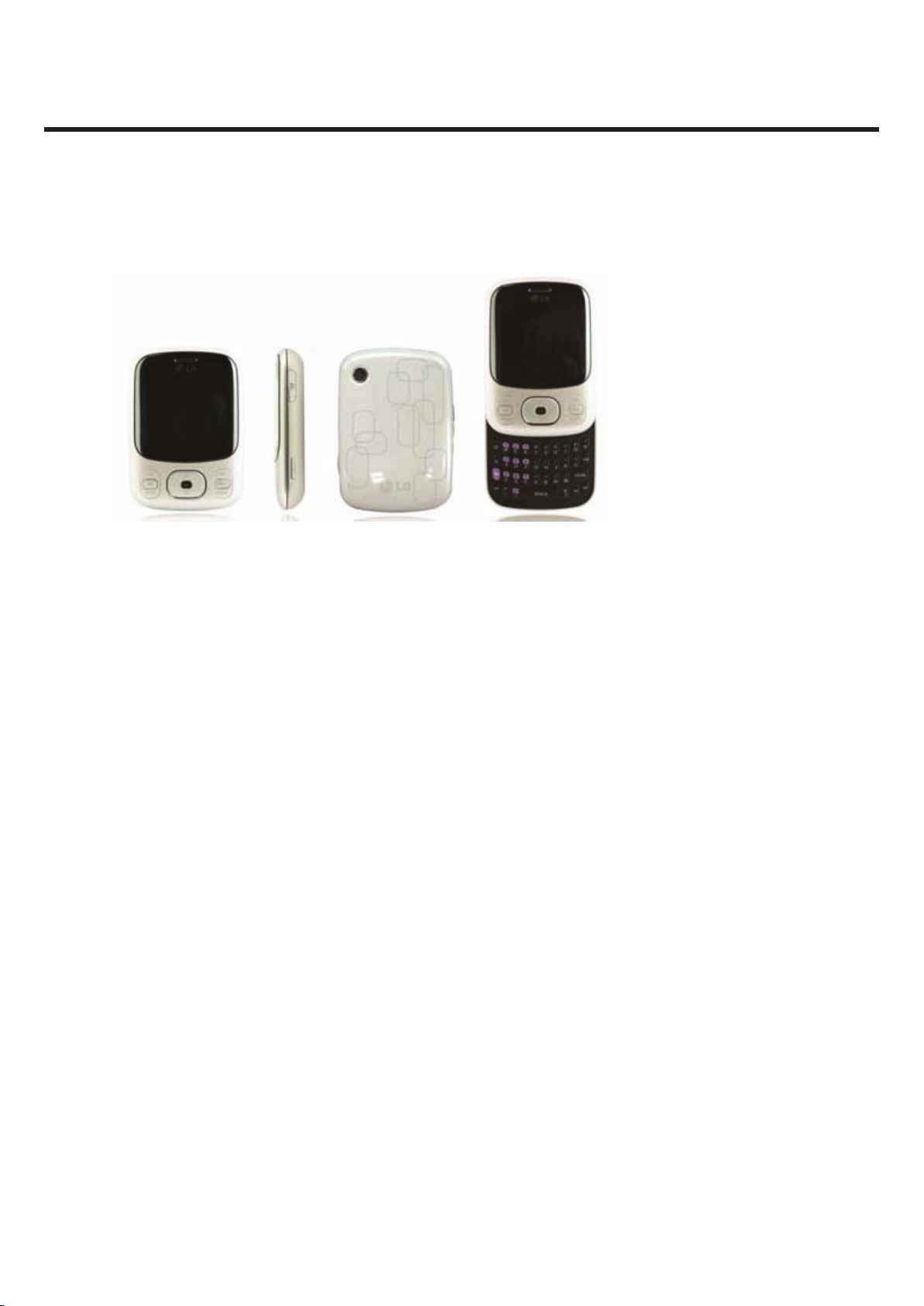
2.7 C320 Figures
2. PERFORMANCE
Copyright © 2010 LG Electronics. Inc. All right reserved.
Only for training and service purposes
- 15 -
LGE Internal Use Only
Page 15
3. TECHNICAL BRIEF
2. Base Band Technical Description
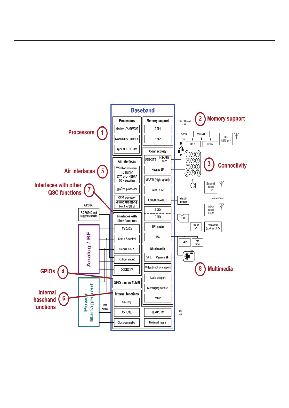
3.1 General Description
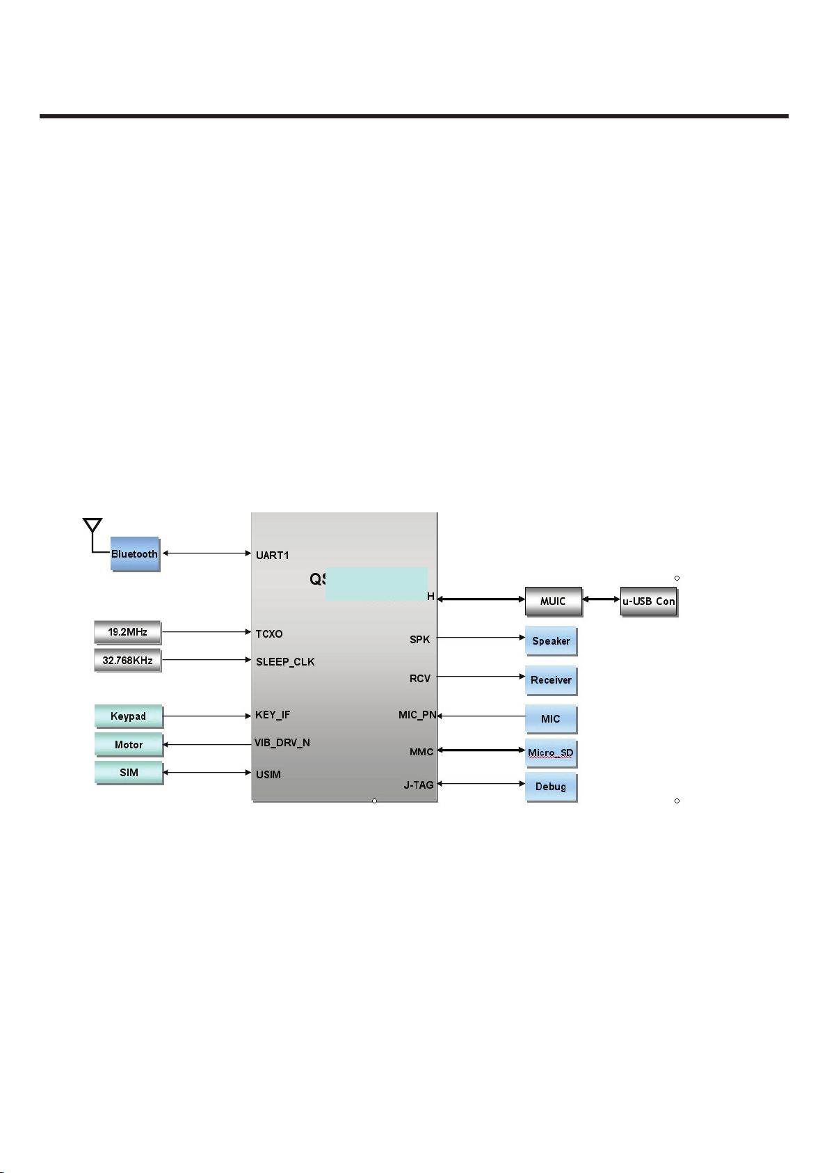
QSC6270 (3G disable)has all eight major functional blocks as like Figure 3.1
Figure 3.1 QSC6270(3G disable) Base band block
3. TECHNICAL BRIEF
LGE Internal Use Only Copyright © 2010 LG Electronics. Inc. All right reserved.
- 16 -
Only for training and service purposes
Page 16
3. TECHNICAL BRIEF
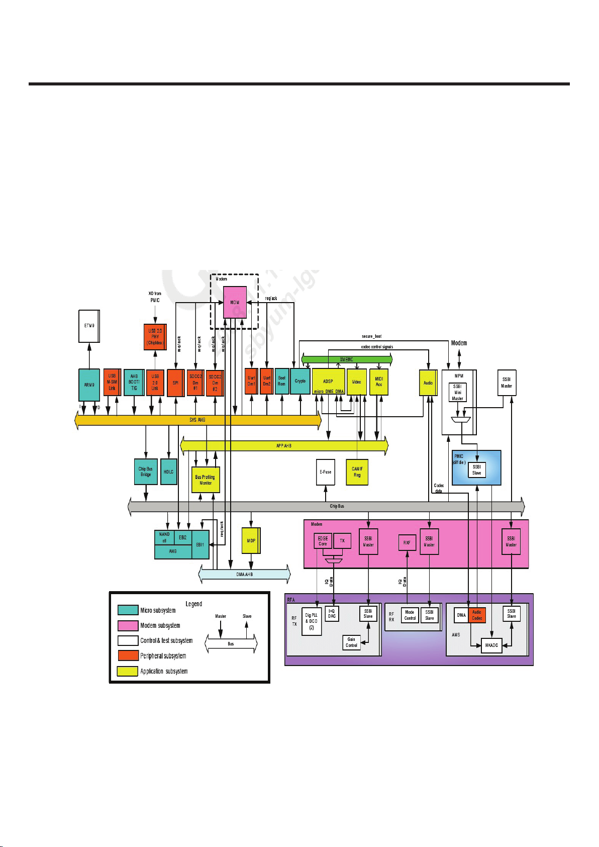
3.1.1 Processor
The QSC6270(3Gdisable) device integrates multiple processors on-chip: one ARM microprocessor and two
DSP processors. Each processor is part of a functional subsystem:
The micro subsystem includes the ARM926EJ-S microprocessor.
The modem subsystem includes the QDSP4u8 digital signal processor (mDSP).
The application subsystem includes the QDSP4u8 application digital signal processor(aDSP).
Figure 3.1.1 Processors and bus architecture
Copyright © 2010 LG Electronics. Inc. All right reserved.
Only for training and service purposes
- 17 -
LGE Internal Use Only
Page 17
3. TECHNICAL BRIEF
3.1.2 Memory support (and LCD interface)
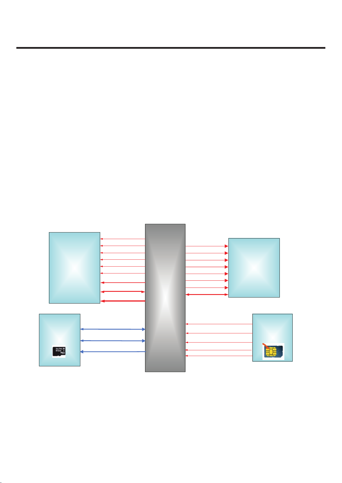
The QSC62x0 device has two external bus interface (EBI) ports: EBI1 and EBI2.
EBI1 supports high-speed synchronous dynamic devices. Its memory controller supports the new mobile
DDR SDRAM memories with its higher bandwidth and ability to run at high clock frequencies. This
interface supports the high-bandwidth, high-density, and low-latency requirements of the QSC’s
advanced on-chip capabilities such as the ARM9 processor, highperformance graphics, and video
applications.
EBI2 is the slower speed interface intended to support memory devices such as NAND flash and
asynchronous SRAM, peripheral devices such as LCDs, and the UBM receiver for multicast or
broadcast reception (QSC6270 only). In addition, EBI2 is required to support a synchronous-burst
AAD NOR flash to enable a NOR/DDR SDRAM memory configuration because the simultaneous mode
(NOR, SDRAM) is not supported on the EBI1 bus.
The ARM926EJ-S microprocessor is a cached processor and all its accesses to external memory use burst
techniques of four or eight 32-bit words when the memory region is declared to be
cacheable/bufferable. To take advantage of this QSC higher performance feature, data from
memories must satisfy the requirements for these burst accesses.
Figure 3.1.2.1 The memory control blocks of C320
QSC6270
NAND Flash
(1Gbit)
SDRAM
512Mbit)
NAND_DATA[ 0: 15]
NAND__CS__N
NAND_ LB_N
NAND_UB_N
NAND_OE_N
NAND_WE_N
NAND_BSY_N
NAND_WP_N
_CE
ALE
CLE
_RE
_WE
RY_BY
_WP
IO[1: 16]
DDR_ A[0:13]
DDR_M_CLK_N
DDR_CKE[0]_
DDR_CS[0]_N_
DDR_RAS_N
DDR_CAS_N
DDR_WE_N_ _
DDR_DQM[0:1]_
DDR_ D[0:15]
CLK
CKE
_CS
_RAS
_CAS
_WE D
DQM
ADDR
DQ
EBI1
EBI2
(3G disable)
USIM
(SIM PLUS)
SIM_CLK
_ _
SIM_DATA
MUSIM_DM
MUSIM_DP
SIM_RST_N
External
Memory
( MICRO SD)
MSD_D[0:3]
MSD_CMD
MSD_CLK
3.1.2 Memory support (and LCD interface)
The QSC62x0 device has two external bus interface (EBI) ports: EBI1 and EBI2.
EBI1 supports high-speed synchronous dynamic devices. Its memory controller supports the new mobile DDR
SDRAM memories with its higher bandwidth and ability to run at high clock frequencies. This interface supports
the high-bandwidth, high-density, and low-latency requirements of the QSC’s advanced on-chip capabilities such
as the ARM9 processor, highperformance graphics, and video applications.
EBI2 is the slower speed interface intended to support memory devices such as NAND flash and asynchronous
SRAM, peripheral devices such as LCDs, and the UBM receiver for multicast or broadcast reception (QSC6270 only).
In addition, EBI2 is required to support a synchronous-burst AAD NOR flash to enable a NOR/DDR SDRAM memory
configuration because the simultaneous mode (NOR, SDRAM) is not supported on the EBI1 bus.
The ARM926EJ-S microprocessor is a cached processor and all its accesses to external memory use burst
techniques of four or eight 32-bit words when the memory region is declared to be cacheable/bufferable. To take
advantage of this QSC higher performance feature, data from memories must satisfy the requirements for these
burst accesses.
LGE Internal Use Only Copyright © 2010 LG Electronics. Inc. All right reserved.
- 18 -
Only for training and service purposes
Page 18
QSC6270
(3G disable)
QVGA Main
LCD
(2.4", 320x240)
EBI2_DATA[15:0]
LCD_ADS
LCD_CS_N
EBI2_WE_N
LCD_RST
LDO_LCD_2.8V
WLED_PWR
LCD_IF(2:1)
LDO_LCD_1.8V
Figure 3.1.2.2 The LCD interfaces of C320
3. TECHNICAL BRIEF
Copyright © 2010 LG Electronics. Inc. All right reserved.
Only for training and service purposes
- 19 -
LGE Internal Use Only
Page 19
3. TECHNICAL BRIEF
3.1.3 Connectivity
QSC6270 has connectivity features as below
– USB-OTG; USB LS, FS, and HS (2.0 compliant)
– I2C compatible for peripheral controls (1.8 V)
– UART: up to 4 Mbps
– Bluetooth 2.0 support via external SoC
– WLAN via external device (SDIO)
– NFC via external module (I2C)
– FM radio via external module (I2C)
– USIM, SIM, and USB-UICC support; 1.8 and 3 V
– Keypad interface
– SPI (master only) for peripheral support
– Two secure digital controllers — WLAN and secure digital (SD) cards
Figure 3.1.3 The connectivity of BL20
QSC6270
LGE Internal Use Only Copyright © 2010 LG Electronics. Inc. All right reserved.
- 20 -
Only for training and service purposes
Page 20
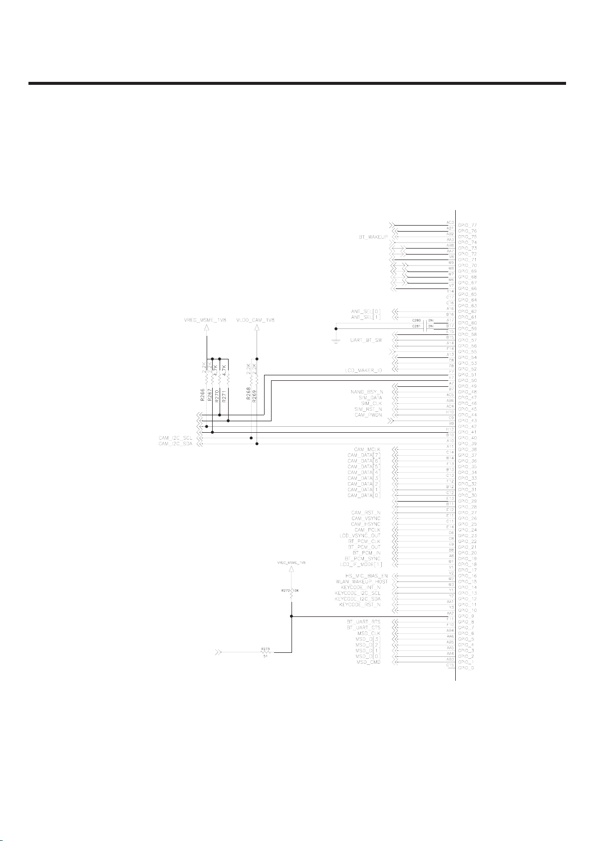
Figure 3.1.4 GPIOs of C320
3.1.4 GPIOs
QSC6270 (3G disable has 78 configurable I/O pins
UART_BT_SEL
MUIC_INT_N
CHG_EN_N
BT_WAKEUP_HOST
CHG_STS_N
HALL_SENS_DET
MUIC_AUD_FM_I2C_SCL
MUIC_AUD_FM_I2C_SDA
BL_LCD_CAM_LDO_I2C_SCL
HS_JACK_DET
WLAN_BT_REG_ON
WLAN_CLK
LCD_IF_MODE[0]
BL_LCD_CAM_LDO_I2C_SDA
WLAN_RST_N
BL_LCD_CAM_LDO_EN
BT_RST_N
WLAN_CMD
LCD_RST_N
WLAN_SDIO[3]
WLAN_SDIO[0]
WLAN_SDIO[1]
WLAN_SDIO[2]
BT_PWR_ON
MUSIM_DM
MUSIM_DP
Low : UART Comm
High : BT UART
3. TECHNICAL BRIEF
Copyright © 2010 LG Electronics. Inc. All right reserved.
Only for training and service purposes
- 21 -
LGE Internal Use Only
Page 21
3. TECHNICAL BRIEF
3.1.5 Air interfaces
The supported air-interface standards and features include: (See the RF technical description)
GSM/GPRS/EDGE Specification Release 4 (3GPP R4)
Enhanced GPS position location using gpsOne (with RGR6240 IC)
Integrated gpsOne functionality, featuring enhancements by SnapTrack®, Inc., to enable a wide variety of
location-based services and applications, including points of interest, personal navigation, and friend finder
Simultaneous-GPS (processes GPS using dedicated circuitry while voice and/or data signals continue to be
processed separately)
1024x searcher, direct facility termination (DFT) accelerator, off-chip RAM for measured data storage
3.1.6 Internal base band functions
Several baseband circuits within the QSC6270(3G disable)device provide functions that are necessary only to
make the device operate properly — these functions are not generally used directly by other
handset circuits and functions.
PLLs and clock generation
Modes and resets
Security
Qfuse
JTAG/ETM
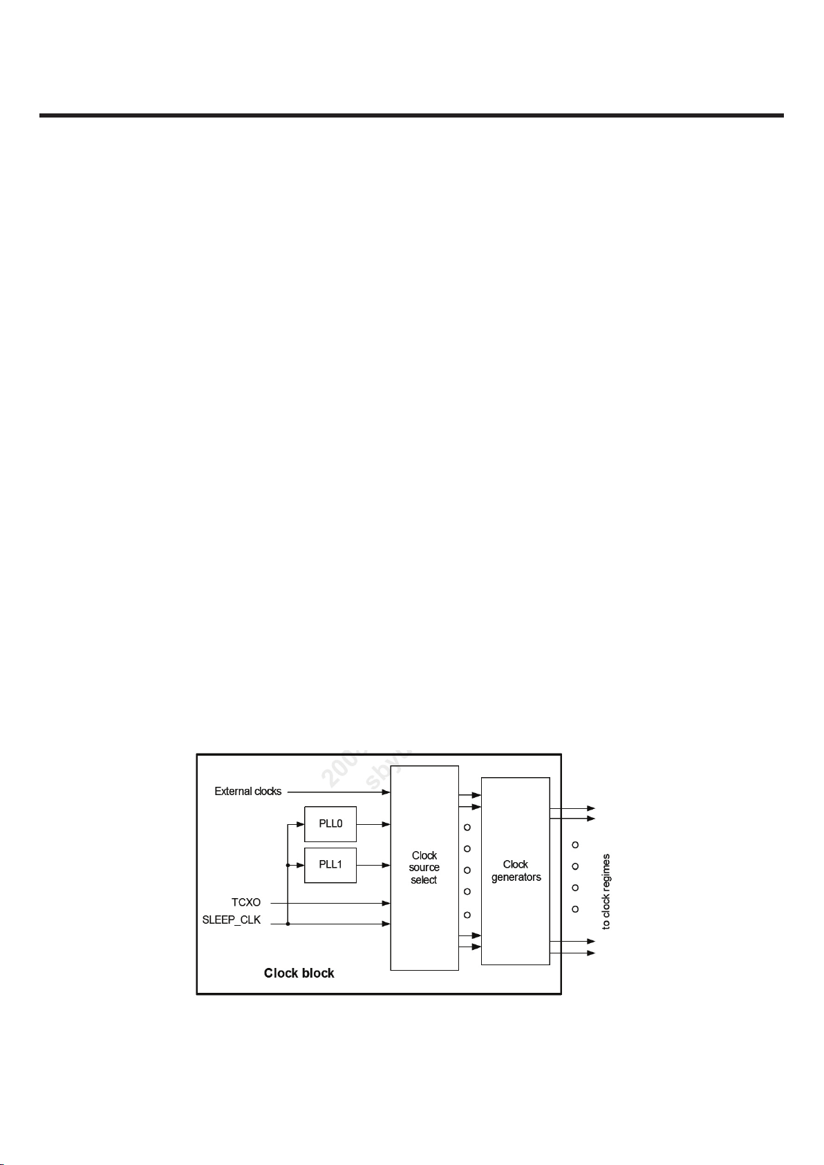
The clock block includes two PLLs, all phase-locked to the TCXO signal. These PLLs generate several
different stable, low-jitter clock signals that are distributed throughout the QSC device and to external c
omponents as needed.
All the required WCDMA, GSM, GPS(only QSC6270), ARM, QDSP, and most peripheral clocks are derived in
some way from the TCXO (or XO) source for their operating modes, plus the 32.768 kHz
oscillator for their sleep modes
Figure 3.1.6 Clock block basic architecture of QSC6270(3G disable)
LGE Internal Use Only Copyright © 2010 LG Electronics. Inc. All right reserved.
- 22 -
Only for training and service purposes
Page 22
3. TECHNICAL BRIEF
3.1.7 Multimedia
Multimedia topics are as below in QSC6270, including:
Camera interface and video front-end
Mobile display processor
Additional multimedia support: video, audio, graphics, and messaging
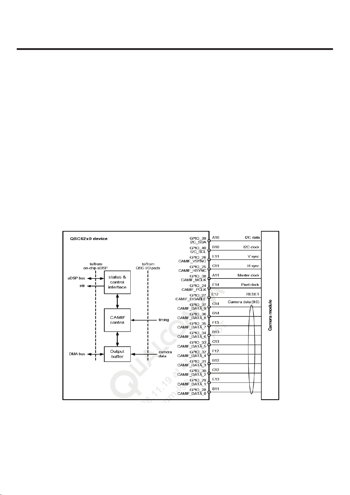
3.1.7.1 Camera interface and video front-end
The camera interface (CAMIF) connects the QSC62x0 device directly to a camera sensor. Typical applications
include Qcamera, Qcamcorder, and QvideophoneThe CAMIF delivers the raw 10-bit Bayer pattern data
(preferred) to the video front-end (VFE) that performs the required image processing (RGB-triplet generation,
color-space conversion, auto-white balance, auto exposure, gamma correction, etc.) and prepares the image
for capture or transmission. The QSC device also supports a YUV 4:2:2 input from the sensor
(8-bit, 2:1 MUX YUV or CCIR656 YUV).
The video capabilities of the two QSC devices varies slightly, with the QSC6270 providing higher performance
than the QSC6270 device — greater resolution, higher capture and streaming rates, etc.
Copyright © 2010 LG Electronics. Inc. All right reserved.
Only for training and service purposes
- 23 -
LGE Internal Use Only
Page 23

3. TECHNICAL BRIEF
3.1.7.2 Mobile display processor
The MDP is a hardware accelerator primarily responsible for transferring an updated image from the QSC
memory subsystem to the LCD module. The transferring of an updated image is an operation that is shared
between software, video processing, and graphics processing, so a common block helps to reduce
redundant circuitry. The MDP is designed with the assumption that the LCD panel has an embedded LCD
controller and a frame buffer. The image transfer is then the copying of the image from the QSC memory
system to the frame buffer within the LCD module.
While the MDP is transferring an image to the LCD module, it can perform a final set of operations to the
image. The set of operations that the MDP can perform has been chosen to maximize the efficiency of the
QSC memory subsystems, typically removing two or more copy operations of the image to and from
memory.
The MDP reduces redundant circuitry and offloads the ARM and aDSP from memory-transfer operations and
a certain set of graphics and video operations
Figure 3.1.7.2.1 MDP-to-LCD interface functional block diagram
LGE Internal Use Only Copyright © 2010 LG Electronics. Inc. All right reserved.
- 24 -
Only for training and service purposes
Page 24
3. TECHNICAL BRIEF
Figure 3.1.7.2.2 The LCD interface of C320
C102
0.1u0.1u
C101
CN102
35
34
33
32
31
30
29
28
27
26
25
24
23
22
21
20
19
18
17
16
15
14
13
12
11
10
9
8
7
6
5
4
3
2
1
1
101R
201R 1
VLDO_LCD_1V8 VLDO_LCD_2V8
LCD_MAKER_ID
LCD_RD
WLED3
WLED2
WLED1
LCD_VSYNC_OUT
LCD_RS
LCD_DATA[7]
LCD_DATA[6]
LCD_DATA[5]
LCD_DATA[4]
LCD_DATA[3]
LCD_DATA[2]
LCD_DATA[1]
LCD_DATA[0]
LCD_WR_N
LCD_CS_N
LCD_RST_N
LCD_DATA[15]
LCD_DATA[14]
LCD_DATA[13]
LCD_DATA[12]
LCD_DATA[11]
LCD_DATA[10]
LCD_DATA[9]
LCD_DATA[8]
LCD_IF_MODE[0]
WLED4
WLED5
LCD_IF_MODE[1]
WLED_VOUT
Copyright © 2010 LG Electronics. Inc. All right reserved.
Only for training and service purposes
- 25 -
LGE Internal Use Only
Page 25

3. TECHNICAL BRIEF
3.1.8 UART
One universal asynchronous receiver transmitter (UART) port that supports low-speed, full-speed,
and high-speed modes
Serial data port communications that conform to the RS-232 interface protocol
Used for data transport during Bluetooth operation (BTS402x™ SoC required)
Other possible uses:
– Test and debug
– External keypad
– Ringer
– Load/upgrade system software
Separate FIFOs for Rx and Tx
Supporting circuits include:
– Interrupt control
– Clock source
– Bit-rate generator (BRG)
– Microprocessor interface
Flow control is not available on UART2 (behind USIM)
3.1.9 USB
Each USB link has a host and a peripheral; the host is responsible for initiating and controlling bus traffic
The USB specification requires PCs to act as hosts, and other devices such as printers, keyboards, mice, etc.,
to act as peripherals
USB 2.0 implementation defines three modes
- Low-speed (LS): 1.5 Mbps
- Full-speed (FS): 12 Mbps
- High-speed (HS): 480 Mbps
The QSC62x0 is compliant with the USB 2.0 specification
- All three modes are supported when acting as a host
- FS and HS are supported when acting as a peripheral
The QSC62x0 has two USB controllers
- Primary USB controller
- Secondary USB controller
The primary USB controller is supplemented by an integrated physical layer (PHY)
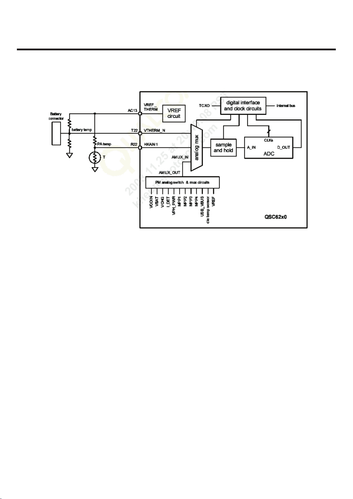
3.1.10 HKADC
The HKADC includes an analog multiplexer that selects an input for the sample and
hold circuit. One of three inputs can be selected:
HKAIN1, pin R22 – an external connection that is available as a general-purpose input,
though it is often used to monitor the power amplifier(s) temperature.
An on-chip connection to the power management circuit’s analog multiplexer output. This allows monitoring of:
-. Key power supply nodes such as VBAT, VCHG, etc.
-. Multipurpose pins (when configured as analog inputs)
-. A few on-chip parameters such as the die temperature or VREF
LGE Internal Use Only Copyright © 2010 LG Electronics. Inc. All right reserved.
- 26 -
Only for training and service purposes
Page 26
3. TECHNICAL BRIEF
QSC6270HKADC Block diagram
Copyright © 2010 LG Electronics. Inc. All right reserved.
Only for training and service purposes
- 27 -
LGE Internal Use Only
Page 27
3. TECHNICAL BRIEF
3.2 Power management
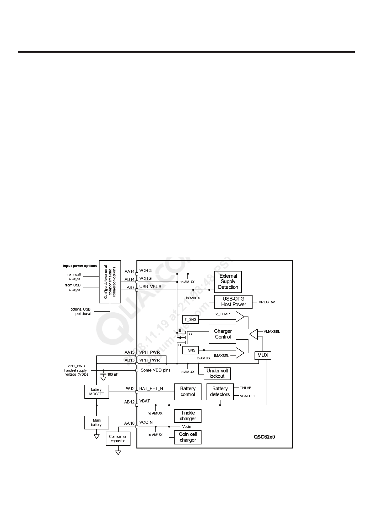
3.2.1 Input power management
Valid external supply attachment and removal detection
Unregulated (closed-loop) external charger supply as input power source
Integrated PFET charging pass transistor; eliminated sense resistor
Support for lithium-ion and lithium-ion polymer main batteries; nickel-based batteries are not supported
Trickle, constant current, constant voltage, and pulse charging of the main battery
Autonomous charging option – driven by an on-chip state machine without software intervention
Software-controlled charging option – backwards-compatible with previous QSC and PM products
Coin-cell battery (including charging)
Battery-voltage detectors with programmable thresholds
VDD collapse protection
Charger-current regulation and real-time monitoring for overcurrent protection
Charger-transistor protection by thermal control
Control drivers for the internal charging PFET and external battery PFET
Voltage, current, and thermal control loops
Automated recovery from sudden momentary power loss (requires external32.768 kHz crystal)
Figure 3.2.1 Input circuits schematic diagram
LGE Internal Use Only Copyright © 2010 LG Electronics. Inc. All right reserved.
- 28 -
Only for training and service purposes
Page 28

3. TECHNICAL BRIEF
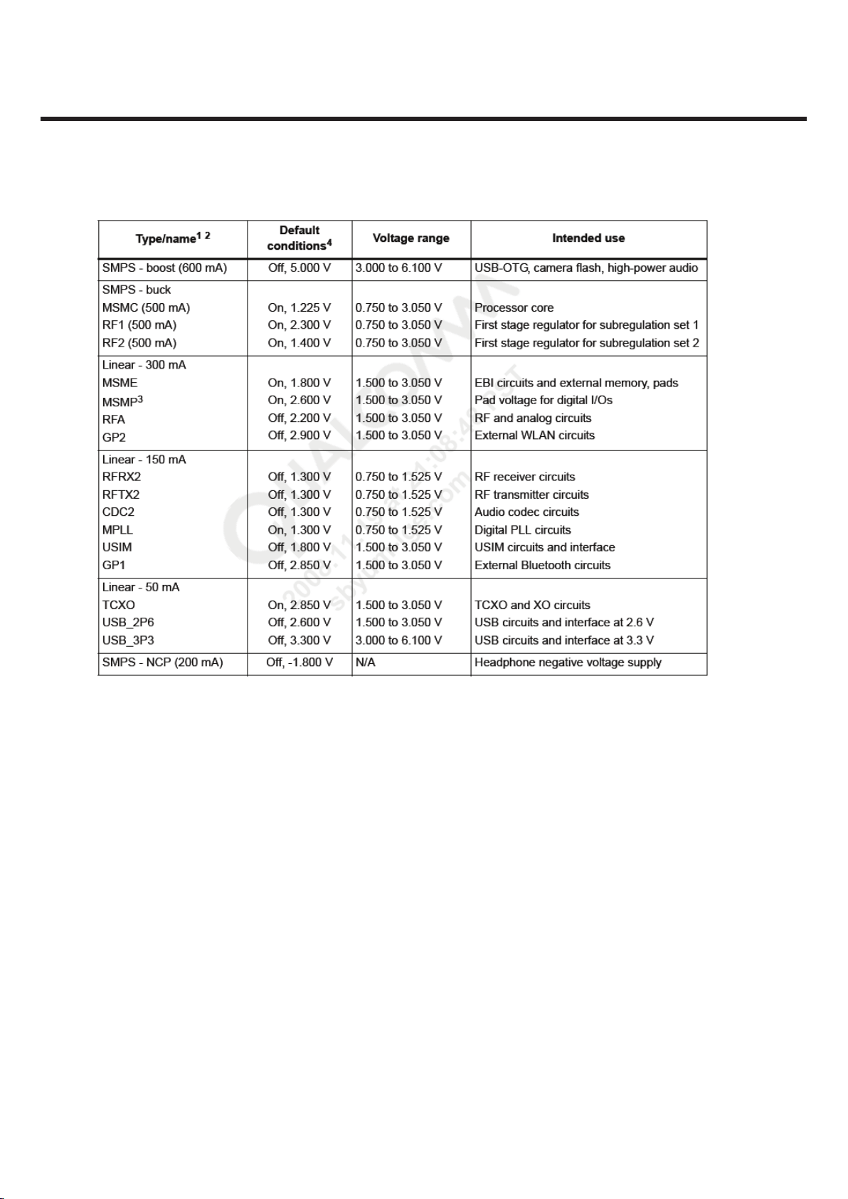
3.2.2 Output voltage regulation
The QSC62x0 device includes all the regulated voltages needed for most low-cost wireless
handset applications (and many other applications). Independent regulated power sources are
required for various electronic functions to avoid signal corruption between diverse circuits,
support power-management sequencing, and meet different voltage-level requirements. Sixteen
voltage regulators are provided — all programmable, all derived from a common bandgap reference circuit.
Three major types of voltage regulator circuits are on-chip:
Three positive voltage switched-mode power supply (SMPS) circuits
- One boost converter (rated for 600 mA)
- Three buck converters (rated for 500 mA each)
Thirteen positive voltage linear regulators
- Four rated for 300 mA
- Six rated for 150 mA
- Three rated for 50 mA
One negative voltage charge pump rated for 200 mA, referred to as a negative charge pump(NCP)
Each regulator has two logic-OR input bits; a logic high at either input enables that regulator:
A master bit that enables all regulators according to their default condition
A dedicated bit that enables only that regulator
The master enable reduces the number of write cycles needed when switching between the phone’s
sleep and active modes.
Additional comments that apply to regulator functions:
If a regulator’s default condition is on, that regulator will power on automatically at QSC startup.
The MSMP regulator must be on to allow internal communications between major functional blocks.
Each regulator and SMPS can provide more than its rated output current, though some
performance characteristics might be degraded.
All regulated output voltages are programmable.
All regulators can be set to a low-power mode except the VREG_USB_3P3 and VREG_NCP circuits
Copyright © 2010 LG Electronics. Inc. All right reserved.
Only for training and service purposes
- 29 -
LGE Internal Use Only
Page 29
3. TECHNICAL BRIEF
Table 3.2.2 Voltage regulator summary
1. All regulator names are based on their intended use, though some may be used to power alternate
functions. For example, the USIM regulator is intended to power an external SIM card but may be used to
power other circuits (or not used at all).
2. Each current listed in this table is its regulator's rated value – the current at which the regulator meets all its
performance specifications. Higher currents are allowed, but higher input voltages may be required and
some performance characteristics may become degraded. See the appropriate regulator sections for details.
3. VREG_MSMP powers key internal circuits and should be kept on at its default voltage setting.
4. All regulators have default output voltage settings, even if they default to an off condition.
LGE Internal Use Only Copyright © 2010 LG Electronics. Inc. All right reserved.
- 30 -
Only for training and service purposes
Page 30

3. TECHNICAL BRIEF
3.2.3 Charging control
C320 use single Charger.
- Single charger has five mode like “ OFF / TRICKLE / ISET / USB500 / FACTORY mode”.
- Single Charger is working as ISET mode in case of CC(Constant Current), CV(Constant Voltage) mode,
as USB 500mode in case of USB Charging.
- FACTORY mode is working only for Factory use.
p
j
j
ylT
kGG
kGuv{G
VBUS_LDO_4V9
I
ND
CHG_STS_N
MUIC_IO_M
MUIC_IO_P
MUIC_ACC_ID
Copyright © 2010 LG Electronics. Inc. All right reserved.
Only for training and service purposes
- 31 -
LGE Internal Use Only
Page 31

3. TECHNICAL BRIEF
3.3 SUB SYSTEM
3.3.1 KEY PAD
C320 have a key-coder IC that supports eight sense lines, or columns, and eight keypad rows.
The device scans and encodes 64 matrix – addressed keys on keypads . Key press and release events are stored
in a FIFO buffer with 16 event lengths for uploading to a host processor. The event data stored will indicate the
sequence of events and which keys set pressed or released.
25pF
25pF
25pF
VREG_MSME_1V8
KEY_COL7
KEY_COL6
LGE Internal Use Only Copyright © 2010 LG Electronics. Inc. All right reserved.
- 32 -
Only for training and service purposes
Page 32

3. TECHNICAL BRIEF
SDRAM
-16-bit low-power DDR SDRAM
-Minimum size per chip-select: 16 MB (128 Mbit)
-Maximum size per chip-select: 128 MB (1 Gbit, 1 k columns only)
Characteristics of the EBI1 clock are listed below:
-Maximum clock rate is 92 MHz, defined by the AMSS software.
-The EBI1 memory controller clock is synchronous to the bus clock (HCLK).
EBI2 Features
EBI2 is used to interface with slower memory and peripheral devices (NAND flash, burst NOR, LCDs, etc.).
The following EBI2 devices are supported:
NAND flash
-8/16 bit, single-level cell (SLC)/multi-level cell (MLC) 512/2048-byte page devices
-DMA support
-Boot-up capability from the above devices
Burst NOR flash
-16-bit multiplexed AAD burst NOR devices
8/16/18-bit (write only) LCD devices (both Motorola and Intel style)
Characteristics of the EBI2 clock are listed below:
The maximum clock rate is 46 MHz, defined by the AMSS software.
The EBI2 memory controller operates at HCLK/2.
Broadcasting and multicasting (QSC6270 only, with MBP1600 IC) are based on:
-Wideband MediaFLO™, DBV-H, and ISDB-T
Asynchronous/burst controller (EBI1 and EBI2)
The external memory controller (xmem_ctlr) forms the asynchronous/burst controller for both EBI1 and EBI2 in
the QSC62x0 device. The controller is generic in terms of its software programmable options and can be
customized when used for EBI1 and EBI2. This block has been enhanced in the QSC62x0 device to support 32-bit
burst memories and byte masking during write operations.
.
3.3.2 External memory interface
The QSC62x0 device has two external bus interface (EBI) ports: EBI1 and EBI2.
EBI1 supports high-speed synchronous dynamic devices. Its memory controller supports the new mobile DDR
SDRAM memories with its higher bandwidth and ability to run at high clock frequencies. This interface supports
the high-bandwidth, high-density, and low-latency requirements of the QSC’s advanced on-chip capabilities
such as the ARM9 processor, highperformance graphics, and video applications.
EBI2 is the slower speed interface intended to support memory devices such as NAND flash and asynchronous
SRAM, peripheral devices such as LCDs, and the UBM receiver for multicast or broadcast reception (QSC6270
only). In addition, EBI2 is required to support a synchronous-burst AAD NOR flash to enable a NOR/DDR SDRAM
memory configuration because the simultaneous mode (NOR, SDRAM) is not supported on the EBI1 bus.
EBI1 Features
EBI1 is a high-performance external memory interface for the QSC62x0 digital block that supports DDR SDRAM
devices Specifically, the following memory devices are supported on EBI1:
Copyright © 2010 LG Electronics. Inc. All right reserved.
Only for training and service purposes
- 33 -
LGE Internal Use Only
Page 33

3. TECHNICAL BRIEF
3.3.3 Camera Interface ( 2M CAMERA )
3.3.3.1 2M CAMERA
C320 Installed a 2M Pixel Camera. Below picture shows the camera board to board connector and
camera I/F signal.
LGE Internal Use Only Copyright © 2010 LG Electronics. Inc. All right reserved.
- 34 -
Only for training and service purposes
Page 34

3. TECHNICAL BRIEF
01
5
64
73
82
91
01
5
64
73
82
91
01
5
64
73
82
91
Copyright © 2010 LG Electronics. Inc. All right reserved.
Only for training and service purposes
- 35 -
LGE Internal Use Only
Page 35

3. TECHNICAL BRIEF
3.3.4 LCD Module (LQ024Q3UX01 : SHARP)
The DM24-DSM04 model is a Color TFT LCD supplied by LG Innotek.
This main Module has a 2.4 inch diagonally measured active display area with 320(RGB) X 240 resolution.
Each pixel is divided into Red, Green and Blue sub-pixels and dots which are arranged in vertical stripes.
Main LCD color is determined with 262k colors signal for each pixel.
The DM24-DSM04 has been designed to apply the interface method that enables low power, high speed, and
high contrast. The DM24-DSM04 is intended to support applications where thin thickness and low power are
critical factors and graphic displays are important
GENERAL DESCRIPTION
LGE Internal Use Only Copyright © 2010 LG Electronics. Inc. All right reserved.
- 36 -
Only for training and service purposes
Page 36

Input Signal and Power : Pin Description ( Input Pin : 35 )
PIN DESCRIPTION
3. TECHNICAL BRIEF
Copyright © 2010 LG Electronics. Inc. All right reserved.
Only for training and service purposes
- 37 -
LGE Internal Use Only
Page 37

3. TECHNICAL BRIEF
LGE Internal Use Only Copyright © 2010 LG Electronics. Inc. All right reserved.
- 38 -
Only for training and service purposes
Page 38

3. TECHNICAL BRIEF
3.3.5 Audio Signal Processing & Interface
Audio signal processing is divided uplink path and downlink path. The uplink path amplifies the audio signal
from MIC and converts this analog signal to digital signal and then transmits it to DBB Chip (QSC6270). This
transmitted signal is reformed to fit in GSM & WCDMA frame format and delivered to RF Chipset. The downlink
path amplifies the signal from DBB chip (QSC6270) and outputs it to receiver (or speaker).
The receive path can be directed to either one of two earphone amplifiers or the auxiliary output. The outputs
earphone1 (EAR1OP, EAR1ON) and auxiliary out (LINE_OP, LINE_ON) are differential outputs. Earphone2 (HPH_L,
HPH_R) is a single-ended output stage designed to drive a headset speaker. The microphone interface consists
of two differential microphone inputs, one differential auxiliary input and a two-stage audio amplifier.
Copyright © 2010 LG Electronics. Inc. All right reserved.
Only for training and service purposes
- 39 -
LGE Internal Use Only
Page 39

3. TECHNICAL BRIEF
G
3.4 GENERAL DESCRIPTION
The RF platform of C320 supports four communication bands (GSM850 / GSM900 / GSM1800 / GSM1900).
The all the RF blocks can be divided into two main parts, which are a GSM, and an antenna switch Mode.
The simplified block diagram is shown in Figure 3.4
[Figure 1.1] Block diagram of RF part
(RF Part)
3.4
LGE Internal Use Only Copyright © 2010 LG Electronics. Inc. All right reserved.
- 40 -
Only for training and service purposes
Page 40

3. TECHNICAL BRIEF
G
3.5 GSM MODE
The EDGE/GPRS/GSM transceiver use a digital interface that is shared between receive and transmit data.
The receive interface is based on I and Q data and the transmitter interface is based on envelop and
frequency data.
The quad band EDGE/GSM/GPRS transceiver has the following general features:
Power class
GMSK low bands: Class 4 (33 dBm)
GMSK high bands: Class 1 (30 dBm)
8PSK low bands: Class E2 (27 dBm)
8PSK high bands: Class E2 (26 dBm)
Multi slot class 12 (4+4=5)
Dual Transfer Mode (DTM) class 9 (3+2=5)
Zero-IF receiver
-Polar modulation transmitter
3.5.1 GSM RECEIVER
The RF receiver designs are leveraged from previous-generation RTR devices, including the latest innovations.
All ESC receiver paths are discussed in this section.
The ZIF receive signal paths support multiband, multimode applications:
Quad-band GSM:
Low-band
GSM 850 (869 to 894 MHz) and GSM 900 (925 to 960 MHz)
High-band
DCS1800 (1805 to 1880 MHz) and PCS1900 (1930 to 1990 MHz)
The on-chip receive signal paths are functionally identical for each mode (GSM or EDGE) and each band type
(low or high). The external circuitry includes the antenna switch module and a filter function.
All RF Rx inputs use a differential configuration to maximize common-mode rejection, Tx isolation, out-ofband suppression, and second-order intermodulation performance. The first of two quadrature
downconverters accepts inputs from two LNAs (only one is active at a time). An example application could
support the following bands using these two LNAs:
GSM 1900
GSM 850
Copyright © 2010 LG Electronics. Inc. All right reserved.
Only for training and service purposes
- 41 -
LGE Internal Use Only
Page 41

3. TECHNICAL BRIEF
G
The second downconverter accepts inputs from another two LNAs (again, just one is active at time) and is
dedicated to GSM 900 and GSM 1800 operation.
The two downconverter outputs drive analog baseband filters and buffer circuits that are programmed to
support the active operating mode’s waveforms (GSM or EDGE). The analog baseband signals are then
digitized by analog-to-digital converters (ADCs) whose outputs are routed to the digital baseband circuits for
further processing.
Numerous secondary Rx functions are also integrated: Rx frequency synthesizers (each having their own PLL
and VCO circuits), LO generation and distribution circuits, reference and clock circuits for the ADCs, and
various interface, control, and status circuits. Power reduction features (such as selective circuit powerdown,
gain control, and bias control) extend handset standby time.
Like the Tx LO, all Rx LO circuits are completely integrated. All received LO signals are generated by the onchip Rx VCOs under control of their PLLs.
[Figure 3.5.1] QSC GSM receiver signal paths functional diagram
LGE Internal Use Only Copyright © 2010 LG Electronics. Inc. All right reserved.
- 42 -
Only for training and service purposes
Page 42

3. TECHNICAL BRIEF
G
3.5.2 GSM TRANSMITTER
The RF transmitters are leveraged from previous-generation RTR™ devices, including the latest innovations.
The ESC transmitter paths and Tx power-detector input are discussed in this section. It provides the zero-IF
(ZIF) transmit signal paths for multiband, multimode applications:
Quad-band GSM:
Low-band
GSM 850 (869 to 894 MHz) and GSM 900 (925 to 960 MHz)
High-band
DCS1800 (1805 to 1880 MHz) and PCS1900 (1930 to 1990 MHz)
The transmit signal paths include a shared set of baseband amplifiers, a dedicated quadrature upconversion
for each band-type (low and high), gain control RF amplification, and multiple output driver amplifiers for
each band-type. Two GSM output drivers support one low-band and one high-band type (but each GSM
band-type is dual-band). The GSM transmitters in polar PA configuration are also supported by a PA envelope
control path, plus the ability to route LO signals to the transmit chains for test and calibration purposes. In
linear PA configuration, phase and envelope paths are combined inside the ESC and amplified using a
multistage linear PA.
Numerous secondary Tx functions are also integrated: a reference for the transmit DACs, the Tx phase-locked
loop (PLL), the Tx OSC circuit, the Tx LO generation and distribution circuits, an RMS Tx power detector, and
various interface, control, and status circuits.
The RF transmitter interfaces internally with the baseband circuits for its analog baseband input and status
and control signaling. Power reduction features controlled by baseband circuits (such as selective circuit
powerdown, gain control, and transmit puncturing) extend handset talk time. The driver amplifier outputs
are routed externally to the final stages of the transmit chains, culminating with the antenna switch whose
output drives the antenna.
Sophisticated Tx LO circuits implement the frequency plan and are completely integrated on-chip. All Tx LO
signals are generated by the on-chip Tx OSC under the control of its PLL.
[Figure 3.5.2] QSC GSM transmitter signal paths functional diagram
Copyright © 2010 LG Electronics. Inc. All right reserved.
Only for training and service purposes
- 43 -
LGE Internal Use Only
Page 43

3. TECHNICAL BRIEF
G
3.6 OFF-CHIP RF COMPONENTS
3.6.1 D5008 (FL101: FEM)
Low-loss SAW frontend module for mobile telephone system
Covering GSM850, GSM900, GSM1800 and GSM1900 bands
Integration of Tx low pass filters, switch, de-coder and diplexing network between GSM Filters
Integration of GSM850, GSM900, GSM1800 and GSM1900 Rx SAWs
Balanced outputs of all Rx ports
Integration of ESD protection at Ant port to 8kV acc. IEC-61000-4-2 (contact discharge)
[Figure 3.6.1] Block diagram of FEM
[Table 3.6.1] Control table of FEM
LGE Internal Use Only Copyright © 2010 LG Electronics. Inc. All right reserved.
- 44 -
Only for training and service purposes
Page 44

3. TECHNICAL BRIEF
G
3.6.2 GSM850/EGSM/DCS/PCS Dual band Transmit Power Amplifier
(U101: SKY77336)
The dual band PA is operating to transmit for low band (GSM-850, GSM-900) and high band (GSM-1800,
GSM1900). Operating mode is selected and controlled by the ESC6270
(GSM_PA_BAND).
[Figure 3.6.2] Block diagram of GSM PAM
Copyright © 2010 LG Electronics. Inc. All right reserved.
Only for training and service purposes
- 45 -
LGE Internal Use Only
Page 45

3. TECHNICAL BRIEF
G
3.7 OFF-CHIP COMPONENTS
3.7.1 Bluetooth (BCM2070)
Bluetooth block of LG-C320 consists of a BCM2070 chip-set, an external crystal oscillator(26MHz), and a
Bluetooth chip antenna (2.4GHz). QSC6270_3G disable, which is main HW solution of LG-C320 Model, doesn’t
include BT baseband core. Instead, Bluetooth chipset, BCM2070, contains stand-alone baseband processor
(V2.1+EDR) as well as BT RF block. An external crystal oscillator (26MHz) is used to provide reference
frequency to BCM2070.
Figure 3.7 shows the Bluetooth system architecture in the LG-C320.
[Figure 3.7] Bluetooth system architecture
LGE Internal Use Only Copyright © 2010 LG Electronics. Inc. All right reserved.
- 46 -
Only for training and service purposes
Page 46

3. TECHNICAL BRIEF
G
[Table 3.7] Bluetooth Connection(GPIO) with QSC6270
Copyright © 2010 LG Electronics. Inc. All right reserved.
Only for training and service purposes
- 47 -
LGE Internal Use Only
Page 47

3. TECHNICAL BRIEF
G
3.7.2 FM Receiver (TEA5991)
The TEA5991 is a single chip FM stereo radio with RDS and RBDS decoder. The radio can be connected to a
headphone antenna and can tune from 70-108 MHz to cover the European, US, Chinese and Japanese FM
band. The radio delivers stereo audio output to an external amplifier. The radio can be controlled with a high
level command based interface through a I2C or SPI-bus.
[Figure3.7.2] shows the FM Radio system architecture in the LGC320.
[Figure3.7.2] FM Radio system architecture
[Figure3.7.2.1] Pin Descriptions
G
ESC6270
AUDIO
SUBSYSTEM
FM
TEA5991
FM_R
FM_L
FM_I2C_SDA
FM_I2C_SDL
HP_R
HP_L
Ear-Jack
FM_ANT
HP_EAR_R
HP_EAR_L
LGE Internal Use Only Copyright © 2010 LG Electronics. Inc. All right reserved.
- 48 -
Only for training and service purposes
Page 48

3. TECHNICAL BRIEF
G
SYMBOL HVQFN WLCSP DESCRIPTION
AGND 1 F1 Analog ground
RFI 2 E1 RF input
RFGND 3 D1 RF ground
NC 4 - not connected
BUSSEL2 5 A1 Bus Selection pin 2
BUSSEL1 6 C1 Bus Selection pin 1
RST 7 A2 Reset, used for operating mode change
SEN 8 B1 Chip Select for SPI bus
SCL 9 A3 Serial Bus Clock
SDA 10 A4 Serial Bus Data
FREF 11 A5 Reference frequency (32.768 kHz)
VREFDIG 12 A6 Reference voltage for digital I/Os
VDD 13 B6 Digital supply voltage
DGND 14 C6 Digital ground
AUDOR 15 D6 Audio output signal right
AUDOL 16 E6 Audio output signal left
NC 17 - Not connected
VCC 18 F6 Analog supply voltage
GPIO2 19 F5 General Purpose I/O 2; Dataout for 4-wire SPI-bus
[Table 3.7.2] pin description
Copyright © 2010 LG Electronics. Inc. All right reserved.
Only for training and service purposes
- 49 -
LGE Internal Use Only
Page 49

4. TROUBLE SHOOTING
5. Base band part
4.1 Power ON Troubleshooting
Power On sequence is :
PWR key press PM_ON_SW_N Î QSC6270 KPDPWR_N pin(AA2) go to low(Main BOARD R205) Î QSC6270
Power Up Î VREG_MSMC_1.2V(C261), VREG_MSME_1.8V(C209), VREG_MSMP_2.6V(C414),
VREG_RFRX2_1.3V(C232), VREG_TCXO_2.85V(C275) power up and system reset assert to QSC6270 Î Phone
booting and PS_HOLD assert to QSC6270
4. TROUBLE SHOOTING
START
Battery voltage. higher
than 3.20V?
Yes
Replaced
with normal LCD module,
and then Booting is OK?
No
TP1_R205 go to low
When Power key press?
Yes
TP2_VREG_MSMC_1.2V(L201)
TP3_VREG_RF1_2.3V(L202)
TP4_VREG_RF1_1.4V(L203)
power up?
Yes
No
Change or charging the Battery
Yes
Go to LCD Troubleshooting
No
Check the Key Dome
No
Change the main board
Change the main board
LGE Internal Use Only Copyright © 2010 LG Electronics. Inc. All right reserved.
- 50 -
Only for training and service purposes
Page 50

TP3TP4TP2TP1
VREG_RF2_1V4|VREG_RF2
N
_WSNO_MP
TP1
TP2
TP3
4. TROUBLE SHOOTING
TP4
Copyright © 2010 LG Electronics. Inc. All right reserved.
Only for training and service purposes
- 51 -
LGE Internal Use Only
Page 51

4. TROUBLE SHOOTING
൯ Charging Procedure
- Connect TA or USB Cable
- Control the charging current by QSC6270(disable 3G)
- Charging current flows into the battery
ත Check Point
- Connection of TA or USB Cable
- Charging current path
- Battery
ත Troubleshooting Setup
- Connect TA and battery to the phone
ත Troubleshooting Procedure
- Check the charger (TA or USB Cable) connector
- Check the charging current Path
- Check the battery
4.2 Charger Troubleshooting
START
Check the pin and battery
Connect terminals of I/O
Connection OK?
Yes
Is the TA voltage TP1_5.1V(FL401)?
Yes
Is it charging properly?
No
Change the main board
connector
No
Change I/O connector
No
Change TA
Yes
END
[ Charger Troubleshooting Flow ]
LGE Internal Use Only Copyright © 2010 LG Electronics. Inc. All right reserved.
- 52 -
Only for training and service purposes
Page 52

4. TROUBLE SHOOTING
FL401
TP1
Copyright © 2010 LG Electronics. Inc. All right reserved.
Only for training and service purposes
TP1
- 53 -
LGE Internal Use Only
Page 53

4. TROUBLE SHOOTING
4.3 USB Troubleshooting
USB Initial sequence is : Isert USB Cable Î USB_VBUS +5V Check Î IC400 triggered USB IF work
START
Cable is insert
physically?
Yes
Is TP1_FL401(VBUS) voltage 5.1V?
Yes
TP2_C409(LDO4.9V)
OUTPUT is about 5V?
Yes
Is IC401 OUTPUT is TP3_C265(USB_
DM,USB_DP) signal OK?
Yes
Change the main board
No
Change CN400
No
Change CN401
No
Change the U401
No
Change the IC401
[ USB Troubleshooting Flow ]
LGE Internal Use Only Copyright © 2010 LG Electronics. Inc. All right reserved.
- 54 -
Only for training and service purposes
Page 54

USB Troubleshooting
kt
kw
TP1 TP2
TP3
FL401
VBUS_LDO_4V9
4. TROUBLE SHOOTING
TP1
TP3
TP2
TP3
Copyright © 2010 LG Electronics. Inc. All right reserved.
Only for training and service purposes
- 55 -
LGE Internal Use Only
Page 55

4. TROUBLE SHOOTING
4.4 USIM Detect Troubleshooting
USIM Initial sequence is :
VREG_USIM_2.85V go to 1.8V or 3.0V Æ USIM_CLK,USIM_RST,USIM_DATA triggered Æ USIM IF work
START
Re-insert the SIM card
Work well ?
No
TP1(Vreg_USIM) is 1.8V or 3.0V ?
TP2(USIM_CLK) & TP3(RST) is run ?
Yes
Change the SIM card
Work well ?
Yes
END
Yes
No
No
END
Check J301
Work well ?
No
Change the Main board
Yes
LGE Internal Use Only Copyright © 2010 LG Electronics. Inc. All right reserved.
- 56 -
Only for training and service purposes
Page 56

TP1 TP3TP2
MUSIM_DM
MUSIM_DP
TP2
4. TROUBLE SHOOTING
TP1
TP3
Copyright © 2010 LG Electronics. Inc. All right reserved.
Only for training and service purposes
- 57 -
LGE Internal Use Only
Page 57

4. TROUBLE SHOOTING
4.5 Camera Troubleshooting
Camera control signals are generated by QSC6270.
START
Check the camera connection to the
socket and reconnect the camera
Camera is OK?
No
CAM_AVDD_2.8V
CAM_VDD_1.8V (TP1, TP2)
Yes
Check the CAM_MCLK
TP4
Check the CAM_PCLK
TP3
Camera is OK
Yes
END
No
Chang the Main board
No
Change the Main board
No
Change the Camera Module
Yes
END
No
Change the Main board
LGE Internal Use Only Copyright © 2010 LG Electronics. Inc. All right reserved.
- 58 -
Only for training and service purposes
Page 58

Camera Troubleshooting
TP1 TP2
TP3
TP4
CAM_70MHz PCLK CAM_24MHz MCLK
Camera Troubleshooting
TP1 TP2
TP3
TP4
4. TROUBLE SHOOTING
TP1
TP3
TP2
TP4
TP4TP3
Copyright © 2010 LG Electronics. Inc. All right reserved.
Only for training and service purposes
- 59 -
LGE Internal Use Only
Page 59

4. TROUBLE SHOOTING
4.6 Main side view LED Troubleshooting
MAIN Key Pad LED is on as below :
Key pressing Æ LED_CON go down low (below 0.8v) Æ MAIN Key Backlight LED On
Key press
START
+VPWR is above 3.2V?
Yes
When the LCD is on,
TP1 is below 0.8v
Yes
LED ON ?
Yes
END
No
Check battery
No
Change QSC6270
No
Change LED
LGE Internal Use Only Copyright © 2010 LG Electronics. Inc. All right reserved.
- 60 -
Only for training and service purposes
Page 60

4.7 Slide Key side view LED Troubleshooting
Sub Key Pad Slide is on as below :
Key pressing Æ LED_CON go down low (below 0.8v) Æ Sub Key Backlight LED On
START
Key press
4. TROUBLE SHOOTING
+VPWR is above 3.2V?
Yes
When the LCD is on,
TP2 is below 0.8v?
Yes
LED ON ?
Yes
END
No
No
No
Check battery
Change the FPCB
or KEY PCB
Change the MAIN PCB
Copyright © 2010 LG Electronics. Inc. All right reserved.
Only for training and service purposes
- 61 -
LGE Internal Use Only
Page 61

4. TROUBLE SHOOTING
LED
TP1
LED
TP2
LD103 LD104 LD105 LD108LD106 LD107
10
R107 R108
10
10
R105 R106
10
10
R109 R110
10
VA101
SLIDE_KEY_LED
WLED_VOUT
SUB KEY B/L
MAIN
SLIDE
TP2
TP1
LGE Internal Use Only Copyright © 2010 LG Electronics. Inc. All right reserved.
- 62 -
Only for training and service purposes
Page 62

4.8 LCD Troubleshooting
LCD control signals are generated by QSC6270.
The signal path is : QSC6270 Æ CN102 Æ LCD Module
START
Press END key
4. TROUBLE SHOOTING
Key LED is on?
Yes
Disconnect and reconnect
The LCD connector
(Slide PCB CN102,CN101)
LCD display OK?
No
Change the FPCB
LCD display OK?
No
Change SUB PCB
No
Yes
Yes
Move to KEY LED Troubleshooting
END
END
LCD display OK?
No
Change the Main Board
Copyright © 2010 LG Electronics. Inc. All right reserved.
Only for training and service purposes
Yes
- 63 -
END
LGE Internal Use Only
Page 63

4. TROUBLE SHOOTING
[Slide Side view placement]
LCD Troubleshooting
LGE Internal Use Only Copyright © 2010 LG Electronics. Inc. All right reserved.
- 64 -
Only for training and service purposes
Page 64

4.9 Vibrator Troubleshooting
Vibrator is operate when DC motor driver is enabled.
START
Operate the Vibrator
4. TROUBLE SHOOTING
CN803(Main B/d)
and CN101(motor_FPCB) are well
connected ?
Yes
Wired
Vibrator to FPCB
”VIB”?
Yes
LINMOT_P
above 3.0V or LINMOT_M
below 1V?
No
Change the FPCB
working?
Yes
No
No
Yes
No
Reconnect Board to FPCB connector
Solder the wire on to FPCB
Change vibrator or
Change the Main PCB
Change vibrator or
Change the Main PCB
END
Copyright © 2010 LG Electronics. Inc. All right reserved.
Only for training and service purposes
- 65 -
LGE Internal Use Only
Page 65

4. TROUBLE SHOOTING
F_SUB_FPCB to Main PCB Connector(CN101)
Main to F_SUB_FPCB Connector(CN803)
1
22
Motor Pad(CN101)
LGE Internal Use Only Copyright © 2010 LG Electronics. Inc. All right reserved.
- 66 -
Only for training and service purposes
Page 66

4.10 Receiver Path
QSC6270(3G disable) EAROP(EARON) Æ TP1_CN801(Main to Slide FPCB Connector) 2,3 PIN
Æ TP2_CN103(=Slide FPCB to Main PCB Connector) 2, 3 PIN Æ TP3_FB101, FB102(of F_SLIDE_ FPCB)
TP4_CN101(= Receiver Pad of F_SLIDE_ FPCB )
START
Connect the phone to network
Equipment and setup call
Setup 1KHz tone out
4. TROUBLE SHOOTING
Can you hear the tone?
No
The sine wave appears at
Receiver Pad(TP4)
No
The sine wave appears at
TP3_FB101, FB102?
No
The sine wave appears at
TP2_CN103 2,3 PIN?
No
The sine wave appears at
TP1_CN801 2,3 PIN?
No
Yes
Yes
Yes
Yes
Yes
END
Re-Solder Receiver
Change the Receiver
Change F_SLIDE_FPCB
Re-Solder FB101,FB102
Change F_SLIDE_FPCB
Re-Connect CN103
Change F_SLIDE_FPCB
Change the QSC6270
Change the Main PCB
Copyright © 2010 LG Electronics. Inc. All right reserved.
Only for training and service purposes
- 67 -
LGE Internal Use Only
Page 67

4. TROUBLE SHOOTING
Main to Slide FPCB Connector(CN801)
1
27
TP1
15pF
15pF
15pF
VCOIN
RCV_P
RCV_N
LCD_DATA[4]
LCD_DATA[5]
LCD_DATA[6]
LCD_DATA[7]
LCD_VSYNC_OUT
LCD_RST_N
LCD_MAKER_ID
TP1
LGE Internal Use Only Copyright © 2010 LG Electronics. Inc. All right reserved.
- 68 -
Only for training and service purposes
Page 68

4. TROUBLE SHOOTING
TP4_Receiver PAD=CN101
1
27
Slide FPCB to Main PCB
Connector(CN103)
TP3_FB101
TP3_FB102
TP2
FB102 100n
10
1
AV
2
0
1C Fp
9
3
101C Fp93
CN101
2
1
2
0
1AV
FB101 100n
RCV_N
RCV_P
Can be Changed to TVS or ECLAMP
CN103
505
514
523
532
541
LCD_MAKER_IDRCV_N
RCV_P LCD_DATA[15]
LCD_DATA[14]
TP3
TP3
TP2
TP4
TP4
Copyright © 2010 LG Electronics. Inc. All right reserved.
Only for training and service purposes
- 69 -
LGE Internal Use Only
Page 69

4. TROUBLE SHOOTING
4.11 Headset path
QSC6270(3G disable) HPH_OUT_L_P/N Æ TP1_C506,C507 Æ IC501(Audio Sub System) Æ
TP2_R504,R505 Æ TP3_FB504, FB505 Æ J501(=3.5pi Ear-jack)
Connect the phone to network
equipment and setup call.
Setup 1KHz tone out and insert headset.
START
Can you hear the tone?
No
Sine wave appears at
TP3_FB504, FB505
No
Sine wave appears at
TP2_R504, R505?
No
Sine wave appears at
TP1_C506, C507?
No
Change the Main board
Yes
Yes
Yes
Yes
END
Re-solder or Change J501
Change the Main PCB
Re-solder the FB504, FB505
Change the Main PCB
Change the IC501
LGE Internal Use Only Copyright © 2010 LG Electronics. Inc. All right reserved.
- 70 -
Only for training and service purposes
Page 70

4. TROUBLE SHOOTING
TP3_FB504
TP3_FB505
TP2_R504
TP2_R505
HS_GND
HS_MIC_P|Hook_ADC
FM_ANT
HS_OUT_R
HS_OUT_L
NC
TP2
TP2
TP3
TP3
Copyright © 2010 LG Electronics. Inc. All right reserved.
Only for training and service purposes
- 71 -
LGE Internal Use Only
Page 71

4. TROUBLE SHOOTING
Audio Sub system IC501TP1_C506TP1_C507
GND
HS_R
SPK_N
SPK_P
MUIC_AUD_FM_I2C_SCL
MUIC_AUD_FM_I2C_SDA
SPK_OUT_
N
SPK_OUT_P
HS_OUT_R
HS_OUT_L
HS_L
WM9093 is possible to 1.8 & 2.6 IO When HPVDD is 1.8V
TP1
TP1
LGE Internal Use Only Copyright © 2010 LG Electronics. Inc. All right reserved.
- 72 -
Only for training and service purposes
Page 72

4.12 Speaker/Speaker Phone path
QSC6270 LINE_OUT_L_P/LINE_OUT_R_N ÆTP1_C508, C509Æ Audio Sub System(IC501) Æ TP2_FB507, FB508 Æ
TP3_CN803 1/2, 3/4 PIN(=Main to F_SUB_FPCB Connector) Æ TP4_CN101 1,2 PIN(=F_SUB_FPCB to Main PCB
Connector) Æ TP5_CN102(= Speaker Pad of F_SUB_FPCB)
START
Connect the phone to network
Equipment and setup call
Setup 1KHz tone out
4. TROUBLE SHOOTING
Can you hear the tone?
No
Sine wave appears at
TP5_Speaker Pad
No
Sine wave appears at
TP4_CN101 1,2 PIN
No
Sine wave appears at
TP3_CN803 1/2, 3/4 PIN
No
Sine wave appears at
TP2_FB507, FB508
No
Sine wave appears at
TP1_C508, C509
Yes
Yes
Yes
Yes
Yes
Yes
END
Re-Solder Speaker Pad
Change the Speaker
Change the F_SUB FPCB
Re-Connect the CN101
Change the F_SUB FPCB
Change the Main PCB
Change the IC501
No
Change the QSC6270
Change the Main board
Copyright © 2010 LG Electronics. Inc. All right reserved.
Only for training and service purposes
- 73 -
LGE Internal Use Only
Page 73

4. TROUBLE SHOOTING
TP1_C508
Audio Sub
System(IC501)
TP1_C509 TP2_FB507 TP2_FB508
GND
HS_R
SPK_N
SPK_P
MUIC_AUD_FM_I2C_SCL
MUIC_AUD_FM_I2C_SDA
SPK_OUT_
N
SPK_OUT_P
HS_OUT_R
HS_OUT_L
HS_L
WM9093 is possible to 1.8 & 2.6 IO When HPVDD is 1.8V
TP2
TP2
TP1
TP1
LGE Internal Use Only Copyright © 2010 LG Electronics. Inc. All right reserved.
- 74 -
Only for training and service purposes
Page 74

4. TROUBLE SHOOTING
TP3
Main to F_SUB_FPCB
Connector(CN803)
1
10
TP3
TP3
Copyright © 2010 LG Electronics. Inc. All right reserved.
Only for training and service purposes
- 75 -
LGE Internal Use Only
Page 75

4. TROUBLE SHOOTING
F_SUB_FPCB to Main PCB
Connector(CN101)
1
10
TP4
CN101
1110
129
138
147
156
165
174
183
192
201
G1 G2
G3 G4
MOTOR_POWER_N
SPK_OUT_P
SPK_OUT_N
MSD_D[3]
MSD_D[2]
MSD_D[1]
MSD_CMD
VBAT
MSD_D[0]
MSD_CLK
VREG_MICROSD_3V0
TP4
LGE Internal Use Only Copyright © 2010 LG Electronics. Inc. All right reserved.
- 76 -
Only for training and service purposes
Page 76

4. TROUBLE SHOOTING
TP5_CN102(=Speaker Pad)
2
1
CN102
SPK_OUT_P
SPK_OUT_N
Can be Changed to TVS or ECLAMP
TP5
Copyright © 2010 LG Electronics. Inc. All right reserved.
Only for training and service purposes
- 77 -
LGE Internal Use Only
Page 77

4. TROUBLE SHOOTING
4.13 Main microphone
MIC501 Æ VMIC_BIAS_P(TP1_C526) Æ MAIN_MIC_P(TP2_C261) Æ MIC1P PAD of QSC6270(3G disable)
START
Make a call
MIC_BIAS(TP1_C526)
is about 1.8V?
Yes
Make sound to MIC
Sine wave appears at
TP2_C261?
Yes
Change the Main board
No
No
No
Change the Main board
Change the MIC
Work well?
Yes
END
LGE Internal Use Only Copyright © 2010 LG Electronics. Inc. All right reserved.
- 78 -
Only for training and service purposes
Page 78

MIC501
TP1_C526
TP2_C261
DNG_CIM
_
N
IA
M
P
_C
I
M_
N
IA
M
TP2
4. TROUBLE SHOOTING
TP1
Copyright © 2010 LG Electronics. Inc. All right reserved.
Only for training and service purposes
- 79 -
LGE Internal Use Only
Page 79

4. TROUBLE SHOOTING
4.14 Headset microphone
3.5 pie Headset ÆHS_MIC_BIAS(TP1_R502) Æ HS_MIC_P(TP2_FB503) Æ HS_MIC_P(TP3_C263)
Æ MIC2P PAD of QSC6270(3G disable)
START
Insert Headset & Make a call
TP1_R502 is About 1.8V ?
Yes
Sine wave appears at
TP2_FB503?
Yes
Sine wave appears at
TP3_C263?
Yes
Change the Headset
Change the MAIN board
No
No
No
Change the LDO(U501)
Change the Main board
Re-Solder FB503
Change the MAIN board
Re-Solder C263
Change the MAIN board
LGE Internal Use Only Copyright © 2010 LG Electronics. Inc. All right reserved.
- 80 -
Only for training and service purposes
Page 80

TP1_R502
TP2_FB503
TP3_C263U501
DNG
_
S
H
TP3
VREG_MSMP_2V6
HS_GND
HS_MIC_P|Hook_ADC
FM_ANT
HS_OUT_R
HS_OUT_L
HS_JACK_DET
´ëüǰ : EUSY0407501
NC
RP183K181D is possible to 1.8 & 2.6 IO
4. TROUBLE SHOOTING
TP1
TP2
Copyright © 2010 LG Electronics. Inc. All right reserved.
Only for training and service purposes
- 81 -
LGE Internal Use Only
Page 81

4. TROUBLE SHOOTING
㝘⪌HG 㵬㦤G 㠄⸬㡸G 㵲㡸G ㍌G 㛺㏩⏼␘UU㝘⪌HG 㵬㦤G 㠄⸬
㡸G 㵲㡸G ㍌G 㛺㏩⏼␘UG
4.15 RF Component
MAIN board Bottom
RF component (GSM)
Reference Description Reference Description
U201 QSC6270 3G disable FL101 FEM
X202 XO SW101 RF connector
U101 GSM(EDGE) TX PAM
FL101
SW101
U101
X202
U201
4.15 RF Component
LGE Internal Use Only Copyright © 2010 LG Electronics. Inc. All right reserved.
- 82 -
Only for training and service purposes
Page 82

4. TROUBLE SHOOTING
㝘⪌HG 㵬㦤G 㠄⸬㡸G 㵲㡸G ㍌G 㛺㏩⏼␘UU㝘⪌HG 㵬㦤G 㠄⸬
㡸G 㵲㡸G ㍌G 㛺㏩⏼␘UG G
G
4.16 RF Path
4.16.1 GSM path
T
X Path
RX Path
T
x/RX Path
4.16 RF Path
Copyright © 2010 LG Electronics. Inc. All right reserved.
Only for training and service purposes
- 83 -
LGE Internal Use Only
Page 83

4. TROUBLE SHOOTING
㝘⪌HG 㵬㦤G 㠄⸬㡸G 㵲㡸G ㍌G 㛺㏩⏼␘UU㝘⪌HG 㵬㦤G 㠄⸬
㡸G 㵲㡸G ㍌G 㛺㏩⏼␘UG G
G
4.17 Trouble Shooting of GSM Part
(GSM850/GSM900/1800/1900)
㝘⪌HG 㵬㦤G 㠄⸬㡸G 㵲㡸G ㍌G 㛺㏩⏼␘UU㝘⪌HG 㵬㦤G 㠄⸬
㡸G 㵲㡸G ㍌G 㛺㏩⏼␘UG G
G
=
LGE Internal Use Only Copyright © 2010 LG Electronics. Inc. All right reserved.
- 84 -
Only for training and service purposes
Page 84

START
Setup Test Equipnment
Cell power = -74dbm
EGSM CH: 38
DCS1800 CH: 698
PCS1900 CH: 661
GSM850 CH: 190
Check M/S & FEM
(SW101 & FL101)
4. TROUBLE SHOOTING
Check
Rx Part
Check
Tx Part
END
Copyright © 2010 LG Electronics. Inc. All right reserved.
Only for training and service purposes
- 85 -
LGE Internal Use Only
Page 85

4. TROUBLE SHOOTING
㝘⪌HG 㵬㦤G 㠄⸬㡸G 㵲㡸G ㍌G 㛺㏩⏼␘UU㝘⪌HG 㵬㦤G 㠄⸬
㡸G 㵲㡸G ㍌G 㛺㏩⏼␘UG G
G
4.17.1 Checking Front-End Module Block
4.17.1 Checking Front-End Module Block
Setup Test Equipnment
Cell power = -74dbm
EGSM CH: 38
DCS1800 CH: 698
PCS1900 CH: 661
GSM850 CH: 190
Check TP3=2.85V?
Yes
Check the logic in each
Mood TP1~TP2 high level
2.85V ≥ Vcc ≥ L4V?
Yes
END
No
No
Check U201
Replace FL101
LGE Internal Use Only Copyright © 2010 LG Electronics. Inc. All right reserved.
- 86 -
Only for training and service purposes
Page 86

4. TROUBLE SHOOTING
㡸G 㵲㡸G ㍌G 㛺㏩⏼␘UG G
G
51
51
51
51
51
51 51
51
850, 900,1800,1900MHz
R109
ANT_FEED
TP4
TP1
TP3
TP2
Copyright © 2010 LG Electronics. Inc. All right reserved.
Only for training and service purposes
- 87 -
LGE Internal Use Only
Page 87

4. TROUBLE SHOOTING
㡸G 㵲㡸G ㍌G 㛺㏩⏼␘UG G
G
51 51 51 51
RX_DCS1800_M
RX_DCS1800_P
RX_GSM850_M
RX_GSM850_P
4.17.2 Checking GSM Rx part
START
Check TP1~TP3
Signal exist?
Yes
Rx still has problem?
Yes
Re-download & calibration
No
Check FEM & Soldeing of TPs
No
GSM Rx is OK
TP1
TP2
TP3
TP4
LGE Internal Use Only Copyright © 2010 LG Electronics. Inc. All right reserved.
- 88 -
Only for training and service purposes
Page 88

4. TROUBLE SHOOTING
㝘⪌HG 㵬㦤G 㠄⸬㡸G 㵲㡸G ㍌G 㛺㏩⏼␘UU㝘⪌HG 㵬㦤G 㠄⸬
㡸G 㵲㡸G ㍌G 㛺㏩⏼␘UG G
G
4.17.3 Checking GSM Tx part
Table 4.17.3 GPAM Logic Control
4.17.3 Checking GSM Tx part
Setup Test Equipnment
Cell power = -60dbm
Tx Power Level Set
GSM850/GSM900 = 5,
DCS/PCS = 0
Yes
Is the level of TP4 same
to Table 4.17.3
Yes
No
Check U201
Yes
TP2, 30dBm over?
TP3, 33dBm over?
Yes
Check TP1,
GSM850, EGSM 32dBm
DCS,PCS 29dBm over?
Yes
Re-download & calibration
No
No
Remove U101 and check
The power of pin1, pin8 (on board)
Yes
The power of pin1, pin8
Replace U101
No
Check U201
Copyright © 2010 LG Electronics. Inc. All right reserved.
Only for training and service purposes
- 89 -
LGE Internal Use Only
Page 89

4. TROUBLE SHOOTING
㝘⪌HG 㵬㦤G 㠄⸬㡸G 㵲㡸G ㍌G 㛺㏩⏼␘UU㝘⪌HG 㵬㦤G 㠄⸬
㡸G 㵲㡸G ㍌G 㛺㏩⏼␘UG G
G
LGE Internal Use Only Copyright © 2010 LG Electronics. Inc. All right reserved.
- 90 -
Only for training and service purposes
Page 90

4. TROUBLE SHOOTING
㝘⪌HG 㵬㦤G 㠄⸬㡸G 㵲㡸G ㍌G 㛺㏩⏼␘UU㝘⪌HG 㵬㦤G 㠄⸬
㡸G 㵲㡸G ㍌G 㛺㏩⏼␘UG G
G
4.18 Checking Bluetooth Block
4.18.1 BLUETOOTH RF components
RF component ( BT )
- Main board bottom -
Reference Description
ANT BT Pattern ANT
U703
BT module_BCM2070
FL701 Band pass filter
X702 26Mhz crystal
U703
X702
FL701
ANT
Copyright © 2010 LG Electronics. Inc. All right reserved.
Only for training and service purposes
- 91 -
LGE Internal Use Only
Page 91

4. TROUBLE SHOOTING
㝘⪌HG 㵬㦤G 㠄⸬㡸G 㵲㡸G ㍌G 㛺㏩⏼␘UU㝘⪌HG 㵬㦤G 㠄⸬
㡸G 㵲㡸G ㍌G 㛺㏩⏼␘UG G
G
4.18.2 BLUETOOTH SIGNAL PATH
Bluetooth Signal PATH (Main board bottom)
Bluetooth T/Rx PATH
LGE Internal Use Only Copyright © 2010 LG Electronics. Inc. All right reserved.
- 92 -
Only for training and service purposes
Page 92

4. TROUBLE SHOOTING
㝘⪌HG 㵬㦤G 㠄⸬㡸G 㵲㡸G ㍌G 㛺㏩⏼␘UU㝘⪌HG 㵬㦤G 㠄⸬
㡸G 㵲㡸G ㍌G 㛺㏩⏼␘UG G
G
4.18.3 BLUETOOTH Trouble shooting
TP# TP description
TP1 VREG_MSMP_2.6V
TP2 VREG_MSME_1.8V
TP3 BT_CLK(26Mhz)
TP4 BT_ANT_OUT
4.18.3 BLUETOOTH Trouble shooting
START
Check TP1, TP2
Signal exist?
No
Change the main board
Yes
Check TP3
IS clock OK?
Yes
Check TP4
Signal exist?
Yes
Change the main board
No
Check X700
No
Check U700
Copyright © 2010 LG Electronics. Inc. All right reserved.
Only for training and service purposes
- 93 -
LGE Internal Use Only
Page 93

4. TROUBLE SHOOTING
㝘⪌HG 㵬㦤G 㠄⸬㡸G 㵲㡸G ㍌G 㛺㏩⏼␘UU㝘⪌HG 㵬㦤G 㠄⸬
㡸G 㵲㡸G ㍌G 㛺㏩⏼␘UG G
G
{wX
{wYG
{wZG
{w[G
WLAN_BT_ANT_FEED
BT_ANT_FEED
Connectivity_ANT_PAD
LGE Internal Use Only Copyright © 2010 LG Electronics. Inc. All right reserved.
- 94 -
Only for training and service purposes
Page 94

4. TROUBLE SHOOTING
㝘⪌HG 㵬㦤G 㠄⸬㡸G 㵲㡸G ㍌G 㛺㏩⏼␘UU㝘⪌HG 㵬㦤G 㠄⸬
㡸G 㵲㡸G ㍌G 㛺㏩⏼␘UG G
G
[BT main clk : 26MHz]
{wX
{wY
{wZ
{w[G
26MHz
A4
C4
E4
D4
RTC_32K
BT_WAKEUP
BT_PCM_CLK
BT_PCM_OUT
BT_PCM_IN
BT_PCM_SYNC
BT_UART_RTS
BT_UART_CTS
BT_WAKEUP_HOST
BT_RST_N
BT_ANT_FEED
RTC_32K768
RTC_32K768
BT_UART_RX
BT_UART_TX
BT_PWR_ON
must have 1% tolerance
can be removed
When power class 1.5 is used, R307 is populated and R308 is depopulated.
(Vice versa for power class 2)
Class 1.5
TP4
TP3
TP2
TP1
Copyright © 2010 LG Electronics. Inc. All right reserved.
Only for training and service purposes
- 95 -
LGE Internal Use Only
Page 95

4. TROUBLE SHOOTING
㝘⪌HG 㵬㦤G 㠄⸬㡸G 㵲㡸G ㍌G 㛺㏩⏼␘UU㝘⪌HG 㵬㦤G 㠄⸬
㡸G 㵲㡸G ㍌G 㛺㏩⏼␘UG G
G
4.19 Checking FM Radio Block
4.19.1 FM Signal Path
Reference Description
U701 TEA5991(FM module)
|^WX
LGE Internal Use Only Copyright © 2010 LG Electronics. Inc. All right reserved.
- 96 -
Only for training and service purposes
Page 96

4.19.2 FM Trouble shooting
START
4. TROUBLE SHOOTING
TP1, TP2 Check the Sianal
Yes
TP3 Check the Signal
Yes
TP4 Check the Signal
Yes
Change the main board
No
Change the main board
No
Change the Ear Jack
No
Change the U601
Copyright © 2010 LG Electronics. Inc. All right reserved.
Only for training and service purposes
- 97 -
LGE Internal Use Only
Page 97

4. TROUBLE SHOOTING
㝘⪌HG 㵬㦤G 㠄⸬㡸G 㵲㡸G ㍌G 㛺㏩⏼␘UU㝘⪌HG 㵬㦤G 㠄⸬
㡸G 㵲㡸G ㍌G 㛺㏩⏼␘UG G
G
TP# TP description
TP1 VREG_MSMP_2.6V
TP2 VREG_MSME_1.8V
TP3 FM_ANT_IN
TP4 FM_OUT_AUDIO signal
XUXU
X
{wYG
{wZG
{w[G
VREG_MSME_1V8
VREG_MSMP_2V6
K2
3_
C
TR
FM_R
L
CS
_
C2
I_
M
F_
D
UA
_C
I
UM
ADS_C2I_MF_DUA_CIUM
FM_L
FM_ANT
Close to QSC
Close to ANT
TP1
TP2
TP3
TP4
TP3
LGE Internal Use Only Copyright © 2010 LG Electronics. Inc. All right reserved.
- 98 -
TP2
TP4
TP1
Only for training and service purposes
Page 98

5. DOWNLOAD
5. DOWNLOAD
LG-C320
Copyright © 2010 LG Electronics. Inc. All right reserved.
Only for training and service purposes
LG-C320
- 99 -
LGE Internal Use Only
Page 99

5. DOWNLOAD
5. DOWNLOAD
LG-C320
LG-C320
LG-C320
LGE Internal Use Only Copyright © 2010 LG Electronics. Inc. All right reserved.
- 100 -
Only for training and service purposes
Page 100

LG-C320
5. DOWNLOAD
LG-C320
Copyright © 2010 LG Electronics. Inc. All right reserved.
Only for training and service purposes
- 101 -
LGE Internal Use Only
 Loading...