

LENOVO Yoga C930 Schematics
5
4
3
2
1
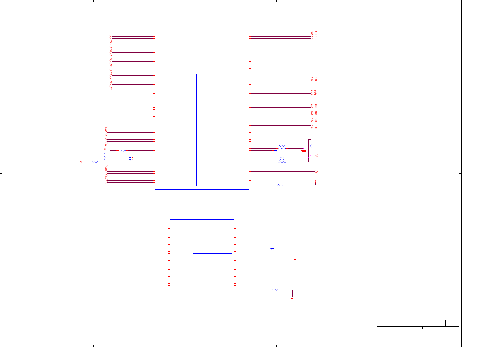
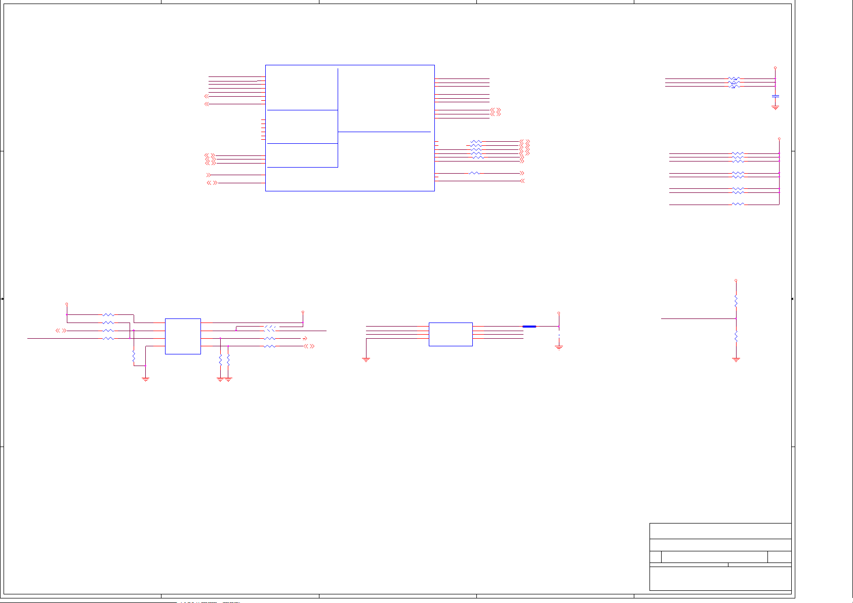
U1 F
AN8
1
UART2_RXD
UART2_TXD
UART2_RTS_N
UART2_CTS_N
AP7
AP8
AR7
AM5
AN7
AP5
AN5
AB1
A
AB3
AD1
AD2
AD3
AD4
AH9
AH10
AH11
AH12
AF11
AF12
BOARD_ID0
BOARD_ID1
BOARD_ID2
BOARD_ID3
BOARD_ID4
B2
W4
U7
U6
U8
U9
M.2_WLAN_WIFI_WAKE_R_N20
RF_KILL_N_WIFI_NGFF20
M.2_WIFI_RST_N20
TP20
BOARD_ID0
R27
100K_0201_5%
1 2
@DDR
R34
100K_0201_5%
1 2
@DDR
BOARD_ID1
BOARD_ID2
BOARD_ID3
TP21TESTPAD
TP22TESTPAD
1 2
1 2
I2C2_SDA
I2C2_SCL
R28
100K_0201_5%
1 2
@DDR
R35
100K_0201_5%
1 2
@DDR
R3849.9K_0201_1% @
R3949.9K_0201_1% @
D D
+3V
I2C0_SDA_TPANEL24
I2C0_SCL_TPANEL24
I2C1_SDA_TPAD26
I2C1_SCL_TPAD26
I2C3_SDA_SENSOR27
I2C3_SCL_SENSOR27
C C
+3V
1 2
@DDR
1 2
@DDR
R24
100K_0201_5%
R31
100K_0201_5%
R25
100K_0201_5%
1 2
@DDR
R32
100K_0201_5%
1 2
@DDR
R26
100K_0201_5%
1 2
@DDR
R33
100K_0201_5%
1 2
@DDR
LPSS ISH
GPP_B15/G SPI0_CS#
GPP_B16/GSPI0_CLK
GPP_B17/G SPI0_MISO
GPP_B18/G SPI0_MOSI
GPP_B19/G SPI1_CS#
GPP_B20/GSPI1_CLK
GPP_B21/G SPI1_MISO
GPP_B22/G SPI1_MOSI
GPP_C8/UART0_RXD
GPP_C9/UART0 _TXD
GPP_C10/U ART0_RTS#
GPP_C11/U ART0_CTS#
GPP_C20/U ART2_RXD
GPP_C21/U ART2_TXD
GPP_C22/U ART2_RTS#
GPP_C23/U ART2_CTS#
GPP_C16/I2C0_SDA
GPP_C17/I2C0_SCL
GPP_C18/I2C1_SDA
GPP_C19/I2C1_SCL
GPP_F4/I2C2_SDA
GPP_F5/I2C2_SCL
GPP_F6/I2C3_SDA
GPP_F7/I2C3_SCL
GPP_F8/I2C4_SDA
GPP_F9/I2C4_SCL
SKL_ULT
SKL_ULT
GPP_D5/ISH_I2C0_SDA
GPP_D6/ISH_I2C0_SCL
GPP_D7/ISH_I2C1_SDA
GPP_D8/ISH_I2C1_SCL
GPP_F10/I2C5_SDA/ISH_I2C2_SDA
GPP_F11/I2C5_SCL/ISH_I2C2_SCL
GPP_D13/I SH_UART0_RXD/ SML0BDATA/I2C4B_ SDA
GPP_D14/ISH_UART0_TXD/SML0BCLK/I2C4B_SCL
6 OF 20
GPP_D15/ISH_UART0_RTS#
GPP_D16/ISH_UART0_CTS#/SML0BALERT#
GPP_C12/UART1_RXD/ISH_UART1_RXD
GPP_C13/UART1_TXD/ISH_UART1_TXD
GPP_C14/UART1_RTS#/ISH_UART1_RTS#
GPP_C15/UART1_CTS#/ISH_UART1_CTS#
GPP_A18/ISH _GP0
GPP_A19/ISH _GP1
GPP_A20/ISH _GP2
GPP_A21/ISH _GP3
GPP_A22/ISH _GP4
GPP_A23/ISH _GP5
GPP_A12/BM_BU SY#/ISH_GP6
I2C2_SDA
I2C2_SCL
GPP_D9
GPP_D10
GPP_D11
GPP_D12
REV= 1
P2
P3
P4
P1
M4
N3
N1
N2
AD11
AD12
U1
U2
U3
U4
AC1
AC2
AC3
AB4
AY8
BA8
BB7
BA7
AY7
AW7
AP13
R16
R17
BM_BUSY_N
BOARD_ID4
12
0_0201_5%
0_0201_5%
12
2
R135 10K_0201_5%@
U5 5
1
VCCA
2
A1
3
A2
GND4OE
PI4ULS5V202XVE_1P2X1P6
AUDIO_PWR_EN 34
TOUCHPANEL_PWR_EN 29
H_DCI_CLK 25
H_DCI_DATA 25
MCU_I2C_SDA_PCH 23
MCU_I2C_SCL_PCH 23
EC_CS_LOWER POWER 27
CCG4_INT_PCH_N 37
FPBACK 24
EC_SENSOR_INT 27
+VCCPGPPA
1
@
8
VCCB
7
B1
6
B2
5
+3VAUX
1
1
100K_0201_5%
1
+3V
1 2
+1.8VAUX
1 2
2
+1.8VDX_SENSORHUB
+3V
V3P0_CCG4_VDDD+1.8VAUX
@
R473 0_0201_5%
2
R476 0_0201_5%@
12
1
CCG4_I2C_PCH_SDA 37
CCG4_I2C_PCH_SCL 37
UART2_RXD
2
R3649.9K_0201_1%
UA RT 2 _T XD
2
R3749.9K_0201_1%
CCG4_INT_PCH_N
R132
2
M.2_WLAN_WIFI_WAKE_R_N
12
R318100K_0201_5%
TOUCHPANEL_PWR_EN
R21610K_0201_5%
AUDIO_PWR_EN
R342410K_0201_5% @
I2C2_SDA
R7532.2K_0201_5% @
12
I2C2_SCL
1
R7522.2K_0201_5% @
I2C3_SDA_SENSOR
12
R7442.2K_0201_5%
I2C3_SCL_SENSOR
12
R7432.2K_0201_5%
12
R202.2K_0201_5%
R212.2K_0201_5%
12
12
R221K_0201_5%
12
R231K_0201_5%
I2C1_SDA_TPAD
I2C1_SCL_TPAD
I2C0_SDA_TPANEL
I2C0_SCL_TPANEL
B B
A A
LENOVO.CRDN
LENOVO.CRDN
1
LENOVO.CRDN
4 50Wednesday, Ju n e 13,2018
4 50Wednesday, Ju n e 13,2018
4 50Wednesday, Ju n e 13,2018
Rev
Rev
Rev
V1.0
V1.0
V1.0
Ti tl e
Ti tl e
Ti tl e
Kaby LakeM CP ( I2C GPIO)
Kaby LakeM CP ( I2C GPIO)
Kaby LakeM CP ( I2C GPIO)
Siz e Document Number
Siz e Document Number
Siz e Document Number
C
C
C
YOGA930
YOGA930
YOGA930
Date: She e t of
Date: She e t of
Date: She e t of
"PROPERTY N OT E : this document contains information confidential and
"PROPERTY N OT E : this document contains information confidential and
"PROPERTY N OT E : this document contains information confidential and
property to LENOVO PND and shall not be reproduced or transferred to other documents
property to LENOVO PND and shall not be reproduced or transferred to other documents
property to LENOVO PND and shall not be reproduced or transferred to other documents
or disclosed to others or used for any purpose other than that for w h ic h it wa s
or disclosed to others or used for any purpose other than that for w h ic h it wa s
or disclosed to others or used for any purpose other than that for w h ic h it wa s
obtained without the expressed wr i t t e n consent of LENOVO PND. "
obtained without the expressed wr i t t e n consent of LENOVO PND. "
obtained without the expressed wr i t t e n consent of LENOVO PND. "
5
4
3
2
5
4
3
2
1
U1 H
PCI E/USB3/ SATA
PCIE_COMP
1
1
H13
PCIE1_RXN/USB3 _5_RXN
G13
PCIE1_RXP/USB3 _5_RXP
B17
PCIE1_TXN/USB3_ 5_TXN
A17
PCIE1_TXP/USB3_ 5_TXP
G11
PCIE2_RXN/USB3 _6_RXN
F11
PCIE2_RXP/USB3 _6_RXP
D16
PCIE2_TXN/USB3_ 6_TXN
C16
PCIE2_TXP/USB3_ 6_TXP
H16
PCIE3_RXN
G16
PCIE3_RXP
D17
PCIE3_TXN
C17
PCIE3_TXP
G15
PCIE4_RXN
F15
PCIE4_RXP
B19
PCIE4_TXN
A19
PCIE4_TXP
F16
PCIE5_RXN
E16
PCIE5_RXP
C19
PCIE5_TXN
D19
PCIE5_TXP
G18
PCIE6_RXN
F18
PCIE6_RXP
D20
PCIE6_TXN
C20
PCIE6_TXP
F20
PCIE7_RXN/SATA0_ RXN
E20
PCIE7_RXP/SATA0_ RXP
B21
PCIE7_TXN/SATA0_TXN
A21
PCIE7_TXP/SATA0_TXP
G21
PCIE8_RXN/SATA1A_ RXN
F21
PCIE8_RXP/SATA1A_ RXP
D21
PCIE8_TXN/SATA1A_TXN
C21
PCIE8_TXP/SATA1A_TXP
E22
PCIE9_RXN
E23
PCIE9_RXP
B23
PCIE9_TXN
A23
PCIE9_TXP
F25
PCIE10_RXN
E25
PCIE10_RXP
D23
PCIE10_TXN
C23
PCIE10_TXP
F5
PCIE_RCOMPN
E5
PCIE_RCOMPP
D56
PROC_PRDY#
D61
PROC_PREQ#
BB11
GPP_A7/PIRQ A#
E28
PCIE11_RXN/ SATA1B_RXN
E27
PCIE11_RXP/SATA1 B_RXP
D24
PCIE11_TXN/SATA1B_ TXN
C24
PCIE11_TXP/SATA1B_ TXP
E30
PCIE12_RXN/ SATA2_RXN
F30
PCIE12_RXP/SATA2 _RXP
A25
PCIE12_TXN/SATA2_ TXN
B25
PCIE12_TXP/SATA2_ TXP
SKL_ULT
PCIE1_TBT_R N35
PCIE1_TBT_R P35
PCIE1_TBT_T N35
D D
TBT
Wlan
PCIE1_TBT_T P35
PCIE2_TBT_R N35
PCIE2_TBT_R P35
PCIE2_TBT_T N35
PCIE2_TBT_T P35
PCIE3_TBT_R N35
PCIE3_TBT_R P35
PCIE3_TBT_T N35
PCIE3_TBT_T P35
PCIE4_TBT_R N35
PCIE4_TBT_R P35
PCIE4_TBT_T N35
PCIE4_TBT_T P35
PCIE5_WLAN_RX_DN20
PCIE5_WLAN_RX_DP20
PCIE5_WLAN_TX_DN20
PCIE5_WLAN_TX_DP20
PCIE Port 9-Port 11 SSD
PCIE9_SSD_RN21
C C
PM_SLP_S0_N8,16,42,43,47
PCIE9_SSD_RP21
PCIE9_SSD_TN21
PCIE9_SSD_TP21
PCIE10_SSD_RN21
PCIE10_SSD_RP21
PCIE10_SSD_TN21
PCIE10_SSD_TP21
PCIE11_SSD_RN21
PCIE11_SSD_RP21
PCIE11_SSD_TN21
PCIE11_SSD_TP21
PCIE12_SSD_RN21
PCIE12_SSD_RP21
PCIE12_SSD_TN21
PCIE12_SSD_TP21
2
R49
0_0201_5%
+VCCPGPPA
R48 100_0201_1%
12
R40
10K_0201_5%
@
1
@
12
TP27TESTPAD
TP28TESTPAD
SKL_ULT
USB2
8 OF 20
SSIC / USB3
USB3_1_RXN
USB3_1_RXP
USB3_1_TXN
USB3_1_TXP
USB3_2_RXN /SSIC_1_RXN
USB3_2_RXP/ SSIC_1_RXP
USB3_2_TXN/SSI C_1_TXN
USB3_2_TXP/SSIC _1_TXP
USB3_3_RXN /SSIC_2_RXN
USB3_3_RXP/ SSIC_2_RXP
USB3_3_TXN/SSI C_2_TXN
USB3_3_TXP/SSIC _2_TXP
USB3_4_RXN
USB3_4_RXP
USB3_4_TXN
USB3_4_TXP
USB2N_1
USB2P_1
USB2N_2
USB2P_2
USB2N_3
USB2P_3
USB2N_4
USB2P_4
USB2N_5
USB2P_5
USB2N_6
USB2P_6
USB2N_7
USB2P_7
USB2N_8
USB2P_8
USB2N_9
USB2P_9
USB2N_10
USB2P_10
USB2_COMP
USB2_ID
USB2_VBUSSENSE
GPP_E9/USB2_ OC0#
GPP_E10/USB2_OC1#
GPP_E11/USB2_OC2#
GPP_E12/USB2_OC3#
GPP_E4/DEVSLP0
GPP_E5/DEVSLP1
GPP_E6/DEVSLP2
GPP_E0/SATAXPCIE0/ SATAGP0
GPP_E1/SATAXPCIE1/ SATAGP1
GPP_E2/SATAXPCIE2/ SATAGP2
GPP_E8/SATALED#
REV= 1
H8
G8
C13
D13
J6
H6
B13
A13
J10
H10
B15
A15
E10
F10
C15
D15
AB9
AB10
AD6
AD7
AH3
AJ3
AD9
AD10
AJ1
AJ2
AF6
AF7
AH1
AH2
AF8
AF9
AG1
AG2
AH7
AH8
AB6
AG3
AG4
A9
C9
D9
B9
J1
J2
J3
H2
H3
G4
H1
US B2 _ CO MP
R47 113_0201_1%
US B2 _ ID
R45 1K_0201_5%
1
USB_ OC_ N1
R41 10K_0201_5%
USB_ OC_ N2
R44 10K_0201_5%
USB_ OC_ N3
R43 10K_0201_5%
TP26 TESTPAD
2
1
USB3_RX1_N 25
USB3_RX1_P 25
USB3_TX1_N 25
USB3_TX1_P 25
USB_ PN1 24
USB_PP1 24
TBTB_USB2_D_ N 39
TBTB_USB2_D_ P 39
USB_ PN5 26
USB_PP5 26
TBTA_USB2_D_ N 38
TBTA_USB2_D_ P 38
USB_ PN7 25
USB_PP7 25
USB_ PN8 20
USB_PP8 20
+3VAUX
12
12
12
12
12
R5010K_0201_5% @
12
R42
10K_0201_5%
USB_ OC_ N0 25
SATA2_DEVSLP 21
+3V
USB3.0 PORT
CAMERA
Finger Print
USB3.0 PORT
BT
B B
A36
CSI2_DN0
B36
CSI2_DP0
C38
CSI2_DN1
D38
CSI2_DP1
C36
CSI2_DN2
D36
CSI2_DP2
A38
CSI2_DN3
B38
CSI2_DP3
C31
CSI2_DN4
D31
CSI2_DP4
C33
CSI2_DN5
D33
CSI2_DP5
A31
CSI2_DN6
B31
CSI2_DP6
A33
CSI2_DN7
B33
CSI2_DP7
A29
CSI2_DN8
B29
CSI2_DP8
C28
CSI2_DN9
D28
CSI2_DP9
A27
CSI2_DN10
B27
CSI2_DP10
C27
CSI2_DN11
D27
CSI2_DP11
A A
5
4
U1 I
CSI-2
SKL_ULT
SKL_ULT
EMMC
GPP_F13/EMMC_DATA0
GPP_F14/EMMC_DATA1
GPP_F15/EMMC_DATA2
GPP_F16/EMMC_DATA3
GPP_F17/EMMC_DATA4
GPP_F18/EMMC_DATA5
GPP_F19/EMMC_DATA6
GPP_F20/EMMC_DATA7
GPP_F21/EMMC_RCLK
9 OF 20
CSI2_CLKN0
CSI2_CLKP0
CSI2_CLKN1
CSI2_CLKP1
CSI2_CLKN2
CSI2_CLKP2
CSI2_CLKN3
CSI2_CLKP3
CSI2_COMP
GPP_D4/FLASHTRIG
GPP_F22/EMMC_CLK
GPP_F12/EMMC_CMD
EMMC_RCO MP
REV= 1
C37
D37
C32
D32
C29
D29
B26
A26
CSI2_COMP
R51 100_0201_1%@
R52 200_0201_1%@
12
12
LENOVO.CRDN
LENOVO.CRDN
1
LENOVO.CRDN
5 50Wednesday, June 13,2018
5 50Wednesday, June 13,2018
5 50Wednesday, June 13,2018
Rev
Rev
Rev
V1.0
V1.0
V1.0
Ti tl e
Ti tl e
Ti tl e
Kaby LakeM CP ( PCIE US B GPIO)
Kaby LakeM CP ( PCIE US B GPIO)
Kaby LakeM CP ( PCIE US B GPIO)
Siz e Document Number
Siz e Document Number
Siz e Document Number
C
C
C
YOGA930
YOGA930
YOGA930
Dat e: She e t of
Dat e: She e t of
Dat e: She e t of
"PROPERTY NO T E: this document contains information confidential and
"PROPERTY N O T E: this document contains information confidential and
"PROPERTY N O T E: this document contains information confidential and
property to LENOVO PND and shall not be reproduced or transferred to other documents
property to LENOVO PND and shall not be reproduced or transferred to other documents
property to LENOVO PND and shall not be reproduced or transferred to other documents
or disclosed to others or used for any purpose other than that for wh i c h it wa s
or disclosed to others or used for any purpose other than that for wh i c h it wa s
or disclosed to others or used for any purpose other than that for wh i c h it wa s
obtained without the expressed written consent of LENOVO PND."
obtained without the expressed written consent of LENOVO PND."
obtained without the expressed written consent of LENOVO PND."
2
E13
B7
AP2
AP1
AP3
AN3
AN1
AN2
AM4
AM1
AM2
AM3
AP4
EMMC_COMP
AT1
3
5
D D
4
3
2
1
SKL_ULT
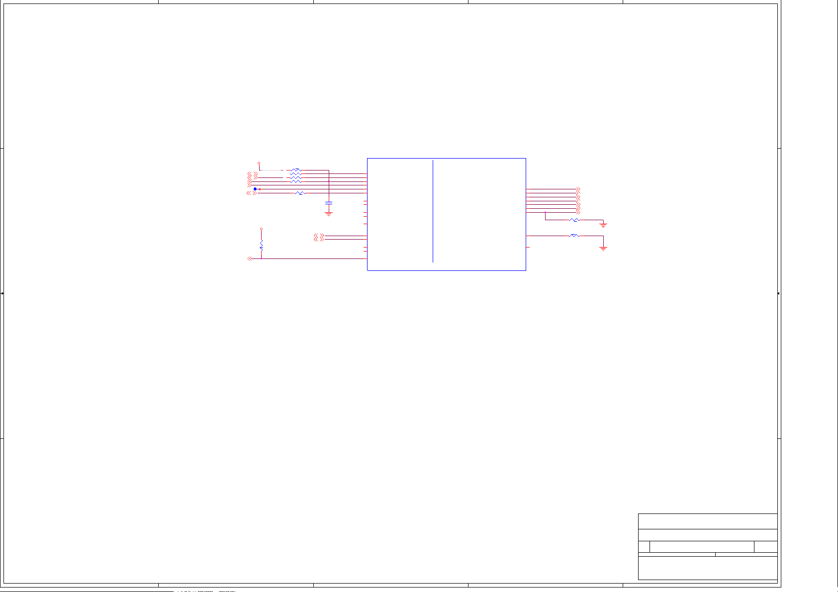
SDIO/ SDXC
GPP_A17/SD_ PWR_EN#/ISH _GP7
7 OF 20
GPP_G0/SD_CMD
GPP_G1/SD_ DATA0
GPP_G2/SD_ DATA1
GPP_G3/SD_ DATA2
GPP_G4/SD_ DATA3
GPP_G5/SD_CD#
GPP_G6/SD_CLK
GPP_G7/SD_WP
GPP_A16/SD_1P8_SEL
SD_RCOMP
GPP_F23
REV= 1
AB11
AB13
AB12
W12
W11
W10
W8
W7
BA9
BB9
AB7
AF13
SD_COMP
1 2
R3425 100K_0201_5%@
2
R57 200_0201_1%@
TBT_CIO_PLUG_EVENT_N 35
TBT_USB_PWR_EN 35
TBT_FORCE_PWR 35
TBT_CIO_PWR _EN 35
TBT_BATLOW_N 35
TBT_WAKE_N 35
TBT_RST_N 35
RTD3
1
BA22
HDA_SYNC/I2S0_SFRM
AY22
HDA_BLK/I2S0_SCLK
BB22
HDA_SDO/I2S0_TXD
BA21
HDA_SDI0/I2S0_RXD
AY21
HDA_SDI1/I2S1_RXD
AW22
HDA_RST#/I2S1_SCLK
J5
GPP_D23/I2S_MCLK
AY20
I2S1_SFRM
AW20
I2S1_TXD
AK7
GPP_F1/I2S2 _SFRM
AK6
GPP_F0/I2S2_SCLK
AK9
GPP_F2/I2S2 _TXD
AK10
GPP_F3/I2S2_RXD
H5
GPP_D19/DMIC_CLK0
D7
GPP_D20/DMIC_DATA0
D8
GPP_D17/DMIC_CLK1
C8
GPP_D18/DMIC_DATA1
AW5
GPP_B14/SPKR
U1 G
SKL_ULT
AUDIO
+VCCPAZIO
HDA_SYNC33
HDA_BCLK33
HDA_SDO33
HDA_SDI33
HDA_RST_N33
C C
PCH_BEEP33
B B
TP29
1
+3V
12
R59
@
1K_0201_5%
1 2
1
1
1
1 2
DMIC_CLK0_PCH24
DMIC_DATA0_PCH24
R581K_0201_5% @
2
R72433_0201_5%
2
R5433_0201_5%
2
R72533_0201_5%
R5333_0201_5% @
2
C3
2P_0201_25V_C
1
A A
LENOVO.CRDN
LENOVO.CRDN
1
LENOVO.CRDN
6 50Wednesday, June 13,2018
6 50Wednesday, June 13,2018
6 50Wednesday, June 13,2018
Rev
Rev
Rev
V1.0
V1.0
V1.0
Ti tl e
Ti tl e
Ti tl e
Kaby LakeM CP ( HDA/I2S/SDIO/DMIC)
Kaby LakeM CP ( HDA/I2S/SDIO/DMIC)
Kaby LakeM CP ( HDA/I2S/SDIO/DMIC)
Siz e Document Number
Siz e Document Number
Siz e Document Number
C
C
C
YOGA930
YOGA930
YOGA930
Dat e: She e t of
Dat e: She e t of
Dat e: She e t of
"PROPERTY N O T E: this document contains information confidential and
"PROPERTY N O T E: this document contains information confidential and
"PROPERTY N O T E: this document contains information confidential and
property to LENOVO PND and shall not be reproduced or transferred to other documents
property to LENOVO PND and shall not be reproduced or transferred to other documents
property to LENOVO PND and shall not be reproduced or transferred to other documents
or disclosed to others or used for any purpose other than that for wh i c h it wa s
or disclosed to others or used for any purpose other than that for wh i c h it wa s
or disclosed to others or used for any purpose other than that for wh i c h it wa s
obtained without the expressed written consent of LENOVO PND."
obtained without the expressed written consent of LENOVO PND."
obtained without the expressed written consent of LENOVO PND."
5
4
3
2
5
Any un-used SRCCLKRQ# signal not mapped to a
Down Device or Connector/ADD-in Card must be
disabled using the Kaby Lake Platform FITC tool
and they must be left as no connects at the CPU
D D
C C
side on the platform
+3V
VCCRTC
SRCCLKREQ2_N
R6110K_0201_5% @
12
SRCCLKREQ4_N
1
2
R6210K_0201_5% @
SRCCLKREQ5_N
1
2
R6310K_0201_5% @
CLK_REQ_TBT_N
1
2
R6610K_0201_5% @
CLK_REQ_WLAN_N
R6410K_0201_5%
12
CLK_REQ_SSD_N
12
R6510K_0201_5%
CLK_SRC1_M.2_SSD_DN21
CLK_SRC1_M.2_SSD_DP21
4
U1 J
CLK_TBT_N35
CLK_TBT_P35
CLK_REQ_TBT_N35
CLK_REQ_SSD_N21
SRCCLKREQ2_N
CLK_WLAN_DN20
CLK_WLAN_DP20
CLK_REQ_WLAN_N20
SRCCLKREQ4_N
SRCCLKREQ5_N
D42
CLKOUT_PCIE_N0
C42
CLKOUT_PCIE_P0
AR10
GPP_B5/SRCCL KREQ0#
B42
CLKOUT_PCIE_N1
A42
CLKOUT_PCIE_P1
AT7
GPP_B6/SRCCL KREQ1#
D41
CLKOUT_PCIE_N2
C41
CLKOUT_PCIE_P2
AT8
GPP_B7/SRCCL KREQ2#
D40
CLKOUT_PCIE_N3
C40
CLKOUT_PCIE_P3
AT10
GPP_B8/SRCCL KREQ3#
B40
CLKOUT_PCIE_N4
A40
CLKOUT_PCIE_P4
AU8
GPP_B9/SRCCL KREQ4#
E40
CLKOUT_PCIE_N5
E38
CLKOUT_PCIE_P5
AU7
GPP_B10/SRC CLKREQ5#
SKL_ULT
SKL_ULT
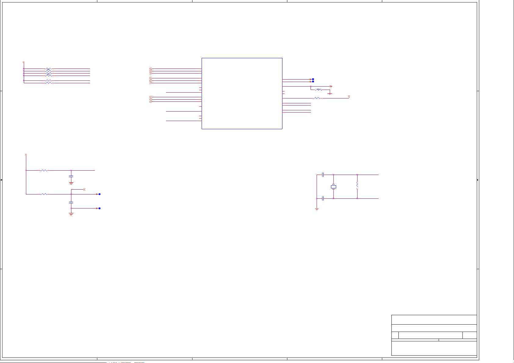
CLOC K S I GN A L S
3
10OF 20
CLKOUT_ITPXDP_N
CLKOUT_ITPXDP_P
GPD8/SUSCLK
XTAL24_IN
XTAL24_OUT
XCLK_BIASREF
RTCX1
RTCX2
SRTCRST#
RTCRST#
REV= 1
F43
E43
BA17
E37
E35
E42
AM18
AM20
AN18
AM16
XCLK_BIASREF
RTC_X1
RTC_X2
SRTC_RST_N
RTC_RST_N
2
R67 1K_0201_5%@
TP32
TP33
R60
TESTPAD
TESTPAD
1
2.7K_0402_0.5%
12
2
SUS_CLK 20,21
+VCCCLK5
1
1 2
R69 20K_0201_1%
1 2
R71 20K_0201_1%
B B
A A
5
SRTC_RST_N
1
C5
1U_0201_10V6K
2
1
C9
1U_0201_10V6K
2
RTC_RST_N 27
ME RESET
SAVE ME = PU (Default)
CLEAR ME = PD
CMOS RESET
TP34
SAVE CMOS = PU (Default)
TESTPAD
CLEAR CMOS = PD
TP34 TP35 Need to put on the TOP
TP35
TESTPAD
4
8.2P_0402_50V8J
1 2
C4
12
Y1
32.768KHZ_9PF_1T JG090DP1AC011
8.2P_0402_50V8J
1 2
C8
3
2
R70
10M_0201_5%
1 2
RTC_X1
RTC_X2
LENOVO.CRDN
LENOVO.CRDN
1
LENOVO.CRDN
7 50Wednesday, June 13,2018
7 50Wednesday, June 13,2018
7 50Wednesday, June 13,2018
Rev
Rev
Rev
V1.0
V1.0
V1.0
Ti tl e
Ti tl e
Ti tl e
Kaby LakeM CP (CLK)
Kaby LakeM CP (CLK)
Kaby LakeM CP (CLK)
Siz e Document Number
Siz e Document Number
Siz e Document Number
C
C
C
YOGA930
YOGA930
YOGA930
Dat e: She e t of
Dat e: She e t of
Dat e: She e t of
"PROPERTY N O T E: this document contains information confidential and
"PROPERTY N O T E: this document contains information confidential and
"PROPERTY N O T E: this document contains information confidential and
property to LENOVO PND and shall not be reproduced or transferred to other documents
property to LENOVO PND and shall not be reproduced or transferred to other documents
property to LENOVO PND and shall not be reproduced or transferred to other documents
or disclosed to others or used for any purpose other than that for wh i c h it wa s
or disclosed to others or used for any purpose other than that for wh i c h it wa s
or disclosed to others or used for any purpose other than that for wh i c h it wa s
obtained without the expressed written consent of LENOVO PND."
obtained without the expressed written consent of LENOVO PND."
obtained without the expressed written consent of LENOVO PND."
5
4
3
2
1
SKL_ULT
SYSTEM POWER MANAGEMEN T
11OF 20
GPP_B12/SLP_S0#
GPD4/SLP_S3 #
GPD5/SLP_S4 #
GPD10/SLP_S5#
SLP_SUS#
SLP_LAN#
GPD9/SLP_W LAN#
GPD6/SLP_A#
GPD3/PWRBTN#
GPD1/ACPRESENT
GPD0/BATLOW#
GPP_A11/PME#
INTRUDER#
GPP_B11/EXT_PWR_GATE#
GPP_B2/VRALER T#
REV= 1
SLP_S0_N
AT11
AP15
BA16
SLP_S5_N
AY16
SLP_SUS_N
AN15
SLP_LAN_N
AW15
BB17
AN16
R220 0_0201_5%@
BA15
AY15
PM_BATLOW_N_R
AU13
AU11
SM_INTRUDER_N
AP16
MPHY_EXT_PWR_GATEB
AM10
AM11
1 2
R89 0_0201_5%
TP45
1
1
TP37
1
TP39
12
SLP_WLAN_N 29
SLP_A_N 27
PCH_PWRBTN_N 27
AC_PRESENT_R 27
1
TP42
1 2
R96 330K_0201_5%
GP_VRALERTB 42
PM_SLP_S0_N 5,16,42,43,47
SLP_S3_N 27,35
SLP_S4_N 27
VCCRTC
PM_BATLOW_N_R
AC_PRESENT_R
PCH_PWRBTN_N
PCIE_WAKE_N
SMC_WAKE_SCI_N
GP_VRALERTB
MPHY_EXT_PWR_GATEB
SLP_WLAN_N
SLP_A_N
PM_RSMRST_N
PLT_RST_N
1 2
R72 8.2K_0201_5%
R73 10K_0201_5%
R74 100K_0201_5%
R75 1K_0201_5%
1 2
R77 10K_0201_5%
1 2
R79 10K_0201_5%@
1 2
R80 20K_0201_5%@
1 2
R81 10K_0201_5%@
1 2
R221 10K_0201_5%@
1 2
R86 100K_0201_5%
1 2
R98 100K_0201_5%
+3VAUX
12
12
12
1K_0201_5%
+3VAUX
+3V
12
R83
SYS_RESET_N
PM_RSMRST_N27
10K_0201_5%
SYS_PWROK_R
PCH_PWROK
2
R3427 10K_0201_5%@
R94
PLT_RST_N16,20,21,27,35
@
0_0201_5%
PCIE_WAKE_N20,21,35
R97 0_0402_5%
R85 0_0402_5%
R82 60.4_0201_1%
R84 0_0201_5%
1
R3429
12
1 2
1 2
1
TP38
1 2
@/VPRO
1 2
0_0201_5%
SMC_WAKE_SCI_N
TP43
1
H_CP UPWR GD
12
SUS_PWR_ACK
SUSACK_N
U1 K
AN10
GPP_B13/PL TRST#
B5
SYS_RESET#
AY17
RSMRST#
A68
PROCPWRGD
B65
VCCST_PWRGD
B6
SYS_PWROK
BA20
PCH_PWROK
BB20
DSW_PWROK
AR13
GPP_A13/SUSW ARN#/SUSPWRDNAC K
AP11
GPP_A15/SUSAC K#
BB15
WAKE#
AM15
GPD2/LAN_ WAKE#
AW17
GPD11/LAN PHYPC
AT15
GPD7/RSVD
SKL_ULT
+VCCST_CPU
1 2
1 2
1 2
12
10K_0201_5%
12
R93
SUS_PWR_ACK_R27
D D
EC_VCCST_PWR GD27
SYS_PWROK27
PM_PCH_PWROK27
C C
R95 0_0402_5%
R87 0_0402_5%
R88 0_0402_5%
12
R78
R76
@
@
100K_0201_5%
B B
A A
LENOVO.CRDN
LENOVO.CRDN
1
LENOVO.CRDN
8 50Wednesday, June 13,2018
8 50Wednesday, June 13,2018
8 50Wednesday, June 13,2018
Rev
Rev
Rev
V1.0
V1.0
V1.0
Ti tl e
Ti tl e
Ti tl e
Kaby LakeM CP (PM)
Kaby LakeM CP (PM)
Kaby LakeM CP (PM)
Siz e Document Number
Siz e Document Number
Siz e Document Number
C
C
C
YOGA930
YOGA930
YOGA930
Dat e: She e t of
Dat e: She e t of
Dat e: She e t of
"PROPERTY N O T E: this document contains information confidential and
"PROPERTY N O T E: this document contains information confidential and
"PROPERTY N O T E: this document contains information confidential and
property to LENOVO PND and shall not be reproduced or transferred to other documents
property to LENOVO PND and shall not be reproduced or transferred to other documents
property to LENOVO PND and shall not be reproduced or transferred to other documents
or disclosed to others or used for any purpose other than that for wh i c h it wa s
or disclosed to others or used for any purpose other than that for wh i c h it wa s
or disclosed to others or used for any purpose other than that for wh i c h it wa s
obtained without the expressed written consent of LENOVO PND."
obtained without the expressed written consent of LENOVO PND."
obtained without the expressed written consent of LENOVO PND."
5
4
3
2
5
4
3
2
1
U1 E
AW13
AY11
AV2
AW3
AV3
W2
A
AU4
AU3
AU2
AU1
M2
M3
J4
V1
V2
M1
G3
G2
G1
SPI - FLASH
SPI0_CLK
SPI0_MISO
SPI0_MOSI
SPI0_IO2
SPI0_IO3
SPI0_CS0#
SPI0_CS1#
SPI0_CS2#
SPI - TOUCH
GPP_D1/SPI1_CLK
GPP_D2/SPI1 _MISO
GPP_D3/SPI1 _MOSI
GPP_D21/SPI 1_IO2
GPP_D22/SPI 1_IO3
GPP_D0/SPI1 _CS#
C LI NK
CL_CLK
CL_DATA
CL_RST#
GPP_A0/RCIN #
GPP_A6/SERIRQ
SKL_ULT
PCH_SCK
D D
PCH_SCE0_N27
PCH_SCE2_N16
CL_CLK20
CL_DATA20
CL_RST_N20
H_RC IN_N27
INT_S ERIR Q27
C C
PCH_SO
PCH_SI
PCH_WP_N
PCH_HOLD_N
SKL_ULT
LPC
5 OF 20
SMBUS, S ML I N K
GPP_A14/SUS_ STAT#/ESPI_RESET#
GPP_C0/SMBCLK
GPP_C1/SMBDATA
GPP_C2/SMBALERT#
GPP_C3/SML0CLK
GPP_C4/SML0 DATA
GPP_C5/SML0 ALERT#
GPP_C6/SML1CLK
GPP_C7/SML1 DATA
GPP_B23/SML1 ALERT#/PCHHO T#
GPP_A1/LAD0 /ESPI_IO0
GPP_A2/LAD1 /ESPI_IO1
GPP_A3/LAD2 /ESPI_IO2
GPP_A4/LAD3 /ESPI_IO3
GPP_A5/LFRAME#/ ESPI_CS#
GPP_A9/CLKO UT_LPC0/ESPI_ CLK
GPP_A10/CL KOUT_LPC1
GPP_A8/CLKRUN#
REV= 1
SMB_CLK
R7
SMB_DATA
R8
SMB_ALERT_N
R10
SML0_CLK
R9
SML0_DATA
W2
SML0_ALERT_N
W1
W3
V3
SML1_ALERT_N
AM7
AY13
1 2
R208 15_0402_5%
BA13
1 2
R218 15_0402_5%
1 2
BB13
R219 15_0402_5%
R327 15_0402_5%
1 2
AY12
BA12
BA11
AW9
AY9
AW11
1 2
R3437 0_0402_5%
R329 15_0402_5%
1 2
SML1_CLK 27
SML1_DATA 27
LPC_AD0_ESPI_IO0 27
LPC_AD1_ESPI_IO1 27
LPC_AD2_ESPI_IO2 27
LPC_AD3_ESPI_IO3 27
LPC_FRAME_N_ESPI_CS_N 27
SUS_STAT_N_ESPI_RST_ N 27
CLK_PCI_LPC_ESPI_CLK 27
PM_CLKRUN_N 27
PM_CLKRUN_N
H_RCIN_N
INT_S ERIR Q
SMB_CLK
SMB_DATA
SMB_ALERT_N
SML0_CLK
SML0_DATA
SML1_CLK
SML1_DATA
SML1_ALERT_N
1 2
R1128.2K_0402_5% @
1
2
R11410K_0402_5% @
1
2
R11510K_0402_5% @
R120 1K_0201_5%
12
12
R122 1K_0201_5%
12
R123 2.2K_0201_5%
R732 499_0402_1%
R731 499_0402_1%
R131 4.7K_0201_5%
12
12
12
R127 1K_0201_5%
R129 1K_0201_5%
12
1 2
+3V
+3VAUX
1
C111U_0201_10V6K
2
HIGH: ESPI IS SELECTED FOR E C
LOW: LPC SELECTED
WEAK INTERNAL PD
+3VAUX
+3VAUX_SPI
1
2
R101150K_0201_5%
PCH_SCE0_N
2
R12820K_0201_5%
PCH_SO_R
R11733_0201_5%
12
PCH_WP_R_N
12
R13033_0201_5%
PCH_SO16,27
PCH_WP_N
1
12
@
B B
R119
100K_0201_5%
U4
1
CS
2
DO
3
WP
GND4DI
W25Q64FVSSIQ_SO8
HOLD
8
VCC
PCH_HOLD_R_N
7
PCH_SCK_R
6
CLK
PCH_SI_R
5
R103150K_0201_5%
1 2
1 2
@
1 2
R133 20K_0201_5%
R134 33_0201_5%
R116 33_0201_5%
R121 33_0201_5%
R124100K_0201_5%
+3VAUX_SPI
U5
PCH_SCE0_N
PCH_HOLD_N
12
12
PCH_SCK 16,27
12
PCH_SI 16,27
PCH_SO_R
PCH_WP_R_N
@/VPRO
1
CS#
2
SO(IO1)
3
WP#(IO2)
4
VSS
W25Q128JVSIQ SOIC
HOLD#(IO3)
SCLK
SI(IO0 )
+3VAUX_SPI
8
PCH_HOLD_R_N
VCC
7
PCH_SCK_R
6
PCH_SI_R
5
1 2
R100 0_0402_5%
+3VALW
2
C10
0.1u_0201_10V6K
1
SML0_ALERT_N
R113
1K_0201_5%
1 2
@
R118
20K_0201_5%
1 2
A A
LENOVO.CRDN
LENOVO.CRDN
1
LENOVO.CRDN
9 50Wednesday, June 13,2018
9 50Wednesday, June 13,2018
9 50Wednesday, June 13,2018
Rev
Rev
Rev
V1.0
V1.0
V1.0
Ti tl e
Ti tl e
Ti tl e
Kaby LakeM CP (LPC SPI SMBCLINK)
Kaby LakeM CP (LPC SPI SMBCLINK)
Kaby LakeM CP (LPC SPI SMBCLINK)
Siz e Document Number
Siz e Document Number
Siz e Document Number
C
C
C
YOGA930
YOGA930
YOGA930
Dat e: She e t of
Dat e: She e t of
Dat e: She e t of
"PROPERTY N O T E: this document contains information confidential and
"PROPERTY N O T E: this document contains information confidential and
"PROPERTY N O T E: this document contains information confidential and
property to LENOVO PND and shall not be reproduced or transferred to other documents
property to LENOVO PND and shall not be reproduced or transferred to other documents
property to LENOVO PND and shall not be reproduced or transferred to other documents
or disclosed to others or used for any purpose other than that for wh i c h it wa s
or disclosed to others or used for any purpose other than that for wh i c h it wa s
or disclosed to others or used for any purpose other than that for wh i c h it wa s
obtained without the expressed written consent of LENOVO PND."
obtained without the expressed written consent of LENOVO PND."
obtained without the expressed written consent of LENOVO PND."
5
4
3
2
5
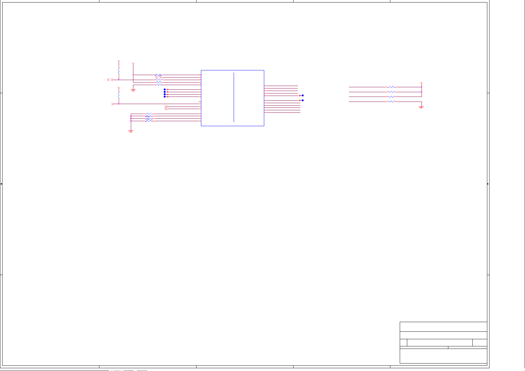
D D
+VCCSTG
+VCCST_CPU
R143
1 2
H_PR OCHO T_ N27,38,39,41,42
TO UCH_P ANEL _INTR _N24
C C
1K_0201_5%
+3V
12
R138
100K_0201_5%
4
1 2
1 2
12
12
12
1
R13749.9_0201_1% @
12
R144499_0402_1%
R1361K_0201_5%
12
R1390_0201_5% @
PECI_EC27
TO UCHPAD _INT R_N26
RF_KILL_N_BT_NGFF20
R151 49.9_0201_1%
R152 49.9_0201_1%
R149 49.9_0201_1%@
2
R150 49.9_0201_1%@
H_CATERR_N
H_PROCHOT_R_N
PCH_THRMTRIP_N
1
TP47
1
TP48
TP49
1
1
TP50
CPU_POPIRCOMP
PCH_POPIRCOMP
OPCE_RCOMP
OPC_RCOMP
AU16
D63
A54
C65
C63
A65
C55
D55
B54
C56
A6
A7
BA5
AY5
AT16
H66
H65
U1 D
CATERR#
PECI
PROCHOT#
THERMTRIP#
SKTOCC#
CPU M I S C
BPM#[0]
BPM#[1]
BPM#[2]
BPM#[3]
GPP_E3/CPU_ GP0
GPP_E7/CPU_ GP1
GPP_B3/CPU_ GP2
GPP_B4/CPU_ GP3
PROC_POPIRCOMP
PCH_OPIRCOMP
OPCE_RCOMP
OPC_RCOMP
SKL_ULT
SKL_ULT
4 OF 20
3
JTAG
PROC_TRST#
PCH_JTAG_TCK
PCH_JTAG_TDI
PCH_JTAG_TDO
PCH_JTAG_TMS
PCH_TRST#
PROC_TCK
PROC_TDI
PROC_TDO
PROC_TMS
JTAGX
REV= 1
PCH_TCK_JTAGX_CPU
B61
PCH_JTAG_TDI_CPU
D60
PCH_JTAG_TDO_CPU
A61
PCH_JTAG_TMS_CPU
C60
XDP_TRST_CPU_N
B59
PCH_JTAG_TCK
B56
PCH_JTAG_TDI_CPU
D59
PCH_JTAG_TDO_CPU
A56
PCH_JTAG_TMS_CPU
C59
XDP_TRST_CPU_N
C61
PCH_TCK_JTAGX_CPU
A59
1
1
TP51 T ESTPAD
TP52 T ESTPAD
2
PCH_JTAG_TDO_CPU
PCH_JTAG_TDI_CPU
PCH_JTAG_TMS_CPU
PCH_TCK_JTAGX_CPU
R140 100_0201_5%
R142 51_0201_5%
12
1 2
R141 51_0201_5%
1 2
12
R146 51_0201_5%
1
+VCCSTG
B B
A A
LENOVO.CRDN
LENOVO.CRDN
1
LENOVO.CRDN
10 50Wednesday,June 13, 2018
10 50Wednesday,June 13, 2018
10 50Wednesday,June 13, 2018
Rev
Rev
Rev
V1.0
V1.0
V1.0
Ti tl e
Ti tl e
Ti tl e
Kaby LakeM CP (MISC THERM CPU JTAG)
Kaby LakeM CP (MISC THERM CPU JTAG)
Kaby LakeM CP (MISC THERM CPU JTAG)
Siz e Document Number
Siz e Document Number
Siz e Document Number
C
C
C
YOGA930
YOGA930
YOGA930
Dat e: She e t of
Dat e: She e t of
Dat e: She e t of
"PROPERTY N O T E: this document contains information confidential and
"PROPERTY N O T E: this document contains information confidential and
"PROPERTY N O T E: this document contains information confidential and
property to LENOVO PND and shall not be reproduced or transferred to other documents
property to LENOVO PND and shall not be reproduced or transferred to other documents
property to LENOVO PND and shall not be reproduced or transferred to other documents
or disclosed to others or used for any purpose other than that for wh i c h it wa s
or disclosed to others or used for any purpose other than that for wh i c h it wa s
or disclosed to others or used for any purpose other than that for wh i c h it wa s
obtained without the expressed written consent of LENOVO PND."
obtained without the expressed written consent of LENOVO PND."
obtained without the expressed written consent of LENOVO PND."
5
4
3
2
5
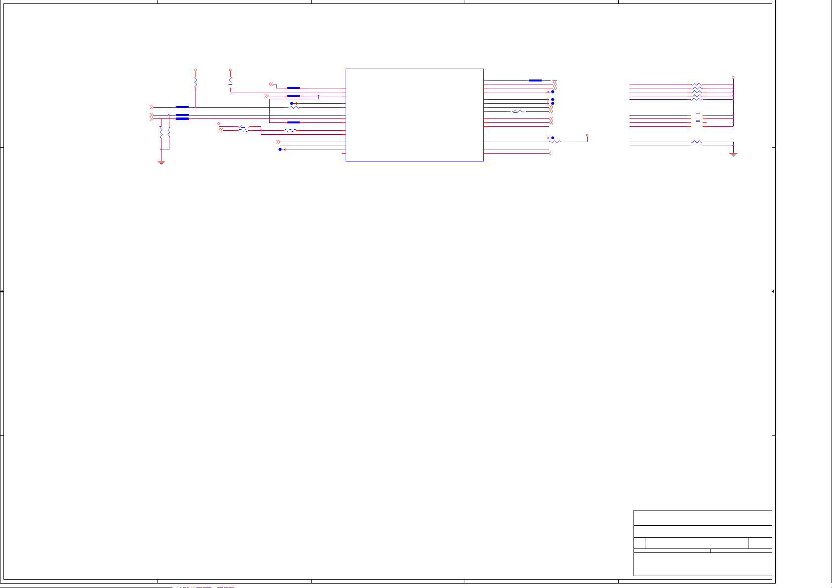
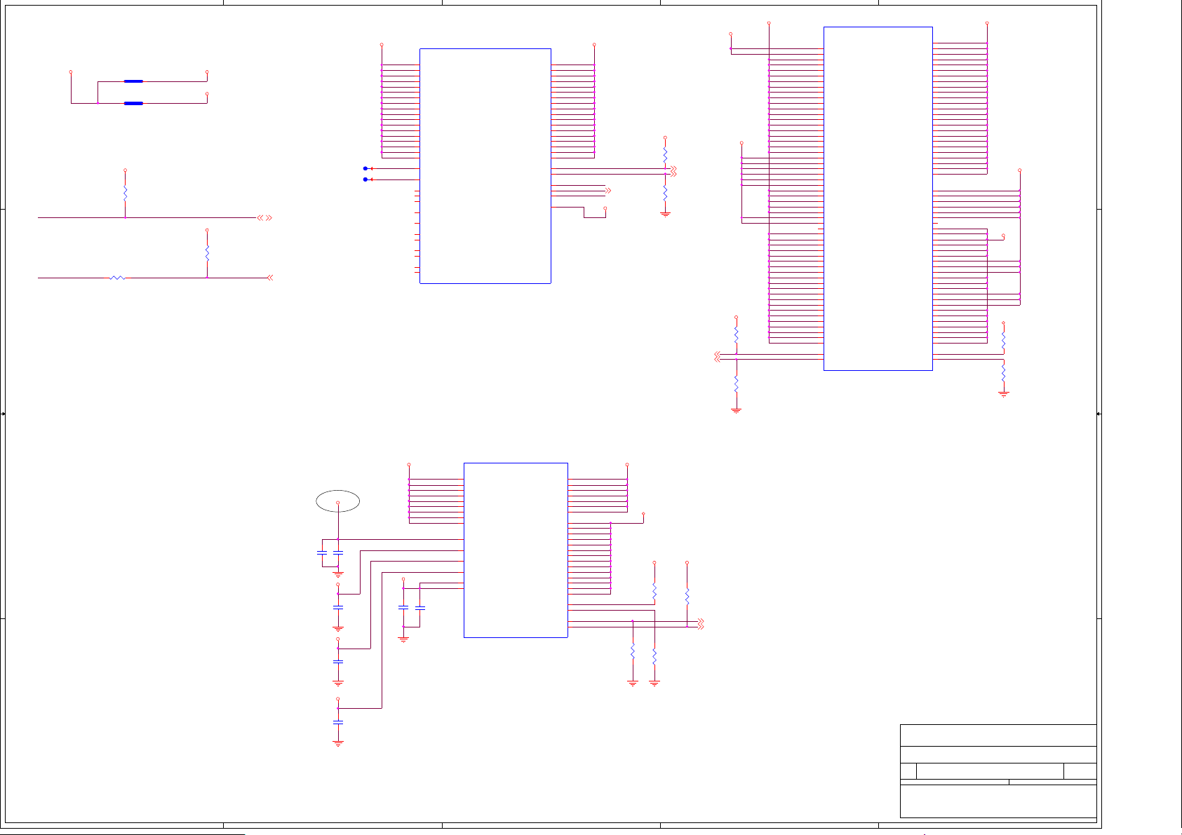
+1.00VDX
D D
VR_SVID_DATA
H_CPU_SVIDALRT_N
C C
1 2
R159 0_0402_5%
R160 0_0402_5%
1 2
+VCCST_CPU
12
R161
100_0201_1%
R167 220_0201_5%
12
+VCCST_CPU
+VCCSTG
+VCCST_CPU
1 2
R166
56_0201_5%
VR_SVID_DATA 42
VR_SVID_ALERT_N 42
4
CPU_CORE CPU_CORE
A30
A34
A39
A44
AK33
AK35
AK37
AK38
AK40
AL33
AL37
AL40
AM32
AM33
AM35
AM37
AM38
G30
1
K32
TP53
1
AK32
TP54
AB62
P62
V62
H63
G61
AC63
AE63
AE62
AG62
AL63
AJ62
SKL_ULT
U1 L
CPU PO WE R 1 OF 4
VCC_A30
VCC_A34
VCC_A39
VCC_A44
VCC_AK33
VCC_AK35
VCC_AK37
VCC_AK38
VCC_AK40
VCC_AL33
VCC_AL37
VCC_AL40
VCC_AM32
VCC_AM33
VCC_AM35
VCC_AM37
VCC_AM38
VCC_G30
RSVD_K32
RSVD_AK32
VCCOPC_AB62
VCCOPC_P62
VCCOPC_V62
VCC_OPC_1P8_H63
VCC_OPC_1P8_G61
VCCOPC_SENSE
VSSOPC_SENSE
VCCEOPIO
VCCEOPIO
VCCEOPIO_SENSE
VSSEOPIO_SENSE
SKL_ULT
12OF 20
VCC_SENSE
VSS_SENSE
VIDALERT#
VCCSTG_G20
VCC_G32
VCC_G33
VCC_G35
VCC_G37
VCC_G38
VCC_G40
VCC_G42
VCC_J30
VCC_J33
VCC_J37
VCC_J40
VCC_K33
VCC_K35
VCC_K37
VCC_K38
VCC_K40
VCC_K42
VCC_K43
VIDSCK
VIDSOUT
REV= 1
3
G32
G33
G35
G37
G38
G40
G42
J30
J33
J37
J40
K33
K35
K37
K38
K40
K42
K43
E32
E33
H_CPU_SVIDALRT_N
B63
A63
VR_SVID_DATA
D64
G20
H_CPU_SVIDCL K 42
+VCCSTG
CPU_CORE
12
12
R157
100_0201_1%
VCC_SENSE 42
VSS_SENSE 42
R158
100_0201_1%
VCCGT_SENSE42
VSSGT_SENSE42
2
GFX_CORE GFX_CORE
CPU_CORE
CPU_CORE
GFX_CORE
12
R162
100_0201_1%
12
R164
100_0201_1%
AA63
AA64
AA66
AA67
AA69
AA70
AA71
AC64
AC65
AC66
AC67
AC68
AC69
AC70
AC71
A48
A53
A58
A62
A66
J43
J45
J46
J48
J50
J52
J53
J55
J56
J58
J60
K48
K50
K52
K53
K55
K56
K58
K60
L62
L63
L64
L65
L66
L67
L68
L69
L70
L71
M62
N63
N64
N66
N67
N69
J70
J69
SKL_ULT
U1 M
CPU POWER 2 O F 4
VCCGT
VCCGT
VCCGT
VCCGT
VCCGT
VCCGT
VCCGT
VCCGT
VCCGT
VCCGT
VCCGT
VCCGT
VCCGT
VCCGT
VCCGT
VCCGT
VCCGT
VCCGT
VCCGT
VCCGT
VCCGT
VCCGT
VCCGT
VCCGT
VCCGT
VCCGT
VCCGT
VCCGT
VCCGT
VCCGT
VCCGT
VCCGT
VCCGT
VCCGT
VCCGT
VCCGT
VCCGT
VCCGT
VCCGT
VCCGT
VCCGT
VCCGT
VCCGT
VCCGT
VCCGT
VCCGT
VCCGT
VCCGT
VCCGT
VCCGT
VCCGT
VCCGT
VCCGT
VCCGT
VCCGT
VCCGT_SENSE
VSSGT_SENSE
SKL_ULT
13OF 20
VCCGTX_AK42
VCCGTX_AK43
VCCGTX_AK45
VCCGTX_AK46
VCCGTX_AK48
VCCGTX_AK50
VCCGTX_AK52
VCCGTX_AK53
VCCGTX_AK55
VCCGTX_AK56
VCCGTX_AK58
VCCGTX_AK60
VCCGTX_AK70
VCCGTX_AL43
VCCGTX_AL46
VCCGTX_AL50
VCCGTX_AL53
VCCGTX_AL56
VCCGTX_AL60
VCCGTX_AM48
VCCGTX_AM50
VCCGTX_AM52
VCCGTX_AM53
VCCGTX_AM56
VCCGTX_AM58
VCCGTX_AU58
VCCGTX_AU63
VCCGTX_BB57
VCCGTX_BB66
VCCGTX_SENSE
VSSGTX_SENSE
REV= 1
VCCGT
VCCGT
VCCGT
VCCGT
VCCGT
VCCGT
VCCGT
VCCGT
VCCGT
VCCGT
VCCGT
VCCGT
VCCGT
VCCGT
VCCGT
VCCGT
VCCGT
VCCGT
VCCGT
VCCGT
VCCGT
VCCGT
VCCGT
VCCGT
VCCGT
N70
N71
R63
R64
R65
R66
R67
R68
R69
R70
R71
T62
U65
U68
U71
W63
W64
W65
W66
W67
W68
W69
W70
W71
Y62
AK42
AK43
AK45
AK46
AK48
AK50
AK52
AK53
AK55
AK56
AK58
AK60
AK70
AL43
AL46
AL50
AL53
AL56
AL60
AM48
AM50
AM52
AM53
AM56
AM58
AU58
AU63
BB57
BB66
AK62
AL61
1
GFX_CORE
GFX_CORE
CPU_CORE
12
@
12
@
R163
100_0201_1%
R165
100_0201_1%
AU23
AU28
AU35
AU42
BB23
BB32
BB41
BB47
BB51
AM40
AL23
A18
A22
K20
K21
U1 N
CPU POWER 3 O F 4
VDDQ_AU23
VDDQ_AU28
VDDQ_AU35
VDDQ_AU42
VDDQ_BB23
VDDQ_BB32
VDDQ_BB41
VDDQ_BB47
VDDQ_BB51
VDDQC
VCCST
VCCSTG_A22
VCCPLL_OC
VCCPLL_K20
VCCPLL_K21
SKL_ULT
SKL_ULT
14OF 20
VCCIO
VCCIO
VCCIO
VCCIO
VCCIO
VCCIO
VCCIO
VCCSA
VCCSA
VCCSA
VCCSA
VCCSA
VCCSA
VCCSA
VCCSA
VCCSA
VCCSA
VCCSA
VCCSA
VCCSA
VCCSA
VCCIO_SENSE
VSSIO_SENSE
VSSSA_SENSE
VCCSA_SENSE
REV= 1
3
AK28
AK30
AL30
AL42
AM28
AM30
AM42
AK23
AK25
G23
G25
G27
G28
J22
J23
J27
K23
K25
K27
K28
K30
AM23
AM22
H21
H20
VCCIO_SENSE
VSSIO_SENSE
100_0201_1%
R170
+VCCIO
12
+VCCSA
12
R171
100_0201_1%
12
R172
100_0201_1%
+VCCSA+VCCIO
12
R168
100_0201_1%
VSSSA_SENSE 42
VCCSA_SENSE 42
LENOVO.CRDN
LENOVO.CRDN
1
LENOVO.CRDN
11 50Wednesday,June 13, 2018
11 50Wednesday,June 13, 2018
11 50Wednesday,June 13, 2018
Rev
Rev
Rev
V1.0
V1.0
V1.0
Ti tl e
Ti tl e
Ti tl e
Kaby LakeM CP (PROCESSOR POWER)
Kaby LakeM CP (PROCESSOR POWER)
Kaby LakeM CP (PROCESSOR POWER)
Siz e Document Number
Siz e Document Number
Siz e Document Number
C
C
C
YOGA920
YOGA920
YOGA920
Dat e: She e t of
Dat e: She e t of
Dat e: She e t of
"PROPERTY N O T E: this document contains information confidential and
"PROPERTY N O T E: this document contains information confidential and
"PROPERTY N O T E: this document contains information confidential and
property to LENOVO PND and shall not be reproduced or transferred to other documents
property to LENOVO PND and shall not be reproduced or transferred to other documents
property to LENOVO PND and shall not be reproduced or transferred to other documents
or disclosed to others or used for any purpose other than that for wh i c h it wa s
or disclosed to others or used for any purpose other than that for wh i c h it wa s
or disclosed to others or used for any purpose other than that for wh i c h it wa s
obtained without the expressed written consent of LENOVO PND."
obtained without the expressed written consent of LENOVO PND."
obtained without the expressed written consent of LENOVO PND."
2
+1.00VDX
C21
1U_0201_10V6K
+1.2VSUS
1
2
2
C22
0.1u_0201_10V6K
1
Note:Layout need to follow
CRB to do an Inductor
+1.2VSUS
B B
1
1
C19
C18
1U_0201_10V6K
1U_0201_10V6K
1U_0201_10V6K
A A
5
0.1u_0201_10V6K
10U_0402_6.3V6M
2
2
+VCCST_CPU
1
C20
2
+VCCSTG
1
C23
2
+1.2V_VCCPLLOC
2
C24
1
4
5
4
3
2
1
SKL_ULT
U1 O
AB19
VCCPRIM_1P0
AB20
VCCPRIM_1P0
P18
VCCPRIM_1P0
AF18
VCCPRIM_CORE
AF19
VCCPRIM_CORE
V20
VCCPRIM_CORE
V21
VCCPRIM_CORE
AL1
DCPDSW_1P0
K17
VCCMPHYAON_1P0
L1
VCCMPHYAON_1P0
N15
VCCMPHYGT_1P0_N15
N16
VCCMPHYGT_1P0_N16
N17
VCCMPHYGT_1P0_N17
P15
VCCMPHYGT_1P0_ P15
P16
VCCMPHYGT_1P0_ P16
K15
VCCAMPHYPLL_1P0
L15
VCCAMPHYPLL_1P0
V15
VCCAPLL_1P0
AB17
VCCPRIM_1P0_ AB17
Y18
VCCPRIM_1P0_Y18
AD17
VCCDSW_3P3_AD17
AD18
VCCDSW_3P3_AD18
AJ17
VCCDSW_3P3_AJ17
AJ19
VCCHDA
AJ16
VCCSPI
AF20
VCCSRAM_1P0
AF21
VCCSRAM_1P0
T19
VCCSRAM_1P0
T20
VCCSRAM_1P0
AJ21
VCCPRIM_3P3_AJ21
AK20
VCCPRIM_1P0_ AK20
N18
VCCAPLLEBB
SKL_ULT
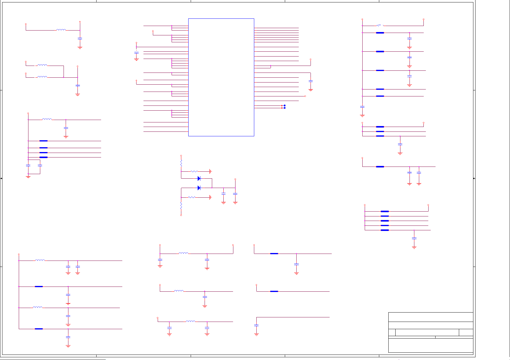
+3VALW
12
R183
3k_0201_1%
R186 45.3K_0201_1%
1 2
CH520N4-45GP_DFN1006-2-2
D1
CH520N4-45GP_DFN1006-2-2
R188 45.3K_0201_1%
1 2
12
R189
0_0402_5%
RTC_VCC
L5
1 2
BLM15GA750SN1D_2P
2 1
D2
2 1
CPU POWER 4 O F 4
2
C44
0.1u_0201_10V6K
1
15OF 20
1
C37
2
VCCRTC
1U_0201_10V6K
+VCCPAZIO
VCCPGPPA
VCCPGPPB
VCCPGPPC
VCCPGPPD
VCCPGPPE
VCCPGPPF
VCCPGPPG
VCCPRIM_3P3_V19
VCCPRIM_1P0_T1
VCCATS_1P8
VCCRTCPRIM_3P3
VCCRTC_AK19
VCCRTC_BB14
DCPRTC
VCCCLK1
VCCCLK2
VCCCLK3
VCCCLK4
VCCCLK5
VCCCLK6
GPP_B0/COR E_VID0
GPP_B1/COR E_VID1
REV= 1
2
C38
0.1u_0201_10V6K
1
AK15
AG15
Y16
Y15
T16
AF16
AD15
V19
T1
AA1
AK17
AK19
BB14
BB10
A14
K19
L21
N20
L19
A10
AN11
AN13
+3VAUX
R195 0_0402_5%
+VCCPGPPA
+VCCPGPPB
+VCCPGPPC
+VCCPGPPD
+VCCPGPPE
+VCCPGPPF
+VCCPGPPG
+VCCPRIM_3P3
+VCCDTS_1P0
+VCCATS_1P8
+VCCPRTCPRIM_3P3
VCCRTCEXT
+VCC19P2_1P0
+VCCCLK2
+VCCCLK3
+VCCCLK4
+VCCCLK6
1
TP55
1
TP56
12
1
C47
1U_0201_10V6K
2
VCCRTC
2
1
+VCCCLK5
C29
0.1u_0201_10V6K
+VCCPRIM_3P3
1 2
@
+VCCMPHYGTAON_1P0_L S
12
+VCCPRIM_CORE
1
C30
1U_0201_10V6K
2
+VCCPRIM_1P0
1
C32
1U_0201_10V6K
2
+VCCMPHYAON_1P0
+VCCDTS_1P0
+VCC19P2_1P0
1
1
C46
C45
1U_0201_10V6K
47U_0603_4V
2
2
PC1
0.1u_0201_10V6K
2.57A
+VCCFHV
3.5A
+VCCMPHYGT_1P0
+VCCDSW_1P0
1U_0201_10V6K
C26
+1.00VAUX
+VCCPRIM_1P0
+VCCPRIM_CORE
1
+VCCMPHYAON_1P0
+VCCMPHYAON_1P0_C
+VCCMPHYGT_1P0
2
+VCCAMPHYPLL_1P0
+VCCAPLL_1P0
+VCCPDSW_3P3
+VCCPAZIO
+VCCPSPI
+VCCSRAM_1P0
+VCCPRIM_3P3
+VCCFHV
+VCCAPLLEBB_1P0
+1.8VAUX
2
C43
2P_0201_25V_C
1
+1.00VAUX
PL1
BLM15PX330SN1D_2P
D D
+1.00VAUX
1 2
L1
BLM15PX330SN1D_2P
+VCCSA
1 2
L2
BLM15PX330SN1D_2P
+1.00VAUX
1 2
L3
BLM15PX121SN1D_2P
C C
R179 0_0402_5%
R182 0_0402_5%
R184 0_0402_5%
R185 0_0402_5%
1
2
B B
+VCCMPHYGTAON_1P0_L S
L6
BLM15PX330SN1D_2P
C544
22U_0402_4V6M
1 2
12
12
12
12
1
C550
22U_0402_4V6M
2
+3VAUX
2
R173 0_0402_5%@
R174 0_0402_5%
R175 0_0402_5%
R176 0_0402_5%
R177 0_0402_5%
R178 0_0402_5%
1
C31
47U_0603_4V
2
+1.8VAUX
R330 0_0402_5%
R180 0_0402_5%
R181 0_0402_5%
+3VAUX
R187 0_0402_5%
+1.00VAUX
R193 0_0402_5%
R190 0_0402_5%
R191 0_0402_5%
R192 0_0402_5%
R194 0_0402_5%
1
12
12
12
12
12
12
12
12
12
12
12
12
12
12
+VCCPGPPF
+VCCATS_1P8
1
C33
1U_0201_10V6K
2
+VCCPGPPA
+VCCPGPPB
1
C25
1U_0201_10V6K
2
+VCCPGPPC
1
C27
1U_0201_10V6K
2
+VCCPGPPE
1
C28
1U_0201_10V6K
2
+VCCPGPPD
+VCCPGPPG
+VCCPGPPA
+VCCPRTCPRIM_3P3
2
1
C35
1U_0201_10V6K
1
2
+VCCCLK2
+VCCCLK3
+VCCCLK4
+VCCCLK6
1
C42
1U_0201_10V6K
2
C36
0.1u_0201_10V6K
+VCCCLK5
+VCCAMPHYPLL_1P0
+VCCSRAM_1P0
+VCCAPLLEBB_1P0
1 2
12
1
C48
1U_0201_10V6K
2
1
C50
1U_0201_10V6K
2
12
1
C51
1U_0201_10V6K
2
5
R196 0_0402_5%
L8
A A
BLM15PX121SN1D_2P
R198 0_0402_5%
+3VAUX
L7
1 2
BLM15PX121SN1D_2P
+1.00VAUX
4
2
C40
2P_0201_25V_C
1
1 2
L4
BLM15GA750SN1D_2P
1
C49
1U_0201_10V6K
2
2
C41
0.1u_0201_10V6K
1
+VCCPDSW_3P3
+VCCAPLL_1P0
+3VAUX_SPI
R197 0_0402_5%
1
C39
1U_0201_10V6K
2
3
+VCCMPHYAON_1P0_C
12
+VCCPSPI
LENOVO.CRDN
LENOVO.CRDN
1
LENOVO.CRDN
12 50Wednesday,June 13, 2018
12 50Wednesday,June 13, 2018
12 50Wednesday,June 13, 2018
Rev
Rev
Rev
V1.0
V1.0
V1.0
Ti tl e
Ti tl e
Ti tl e
Kaby LakeM CP (PCHPOWER)
Kaby LakeM CP (PCHPOWER)
Kaby LakeM CP (PCHPOWER)
Siz e Document Number
Siz e Document Number
Siz e Document Number
C
C
C
YOGA930
YOGA930
YOGA930
Dat e: She e t of
Dat e: She e t of
Dat e: She e t of
"PROPERTY N O T E: this document contains information confidential and
"PROPERTY N O T E: this document contains information confidential and
"PROPERTY N O T E: this document contains information confidential and
property to LENOVO PND and shall not be reproduced or transferred to other documents
property to LENOVO PND and shall not be reproduced or transferred to other documents
property to LENOVO PND and shall not be reproduced or transferred to other documents
or disclosed to others or used for any purpose other than that for wh i c h it wa s
or disclosed to others or used for any purpose other than that for wh i c h it wa s
or disclosed to others or used for any purpose other than that for wh i c h it wa s
obtained without the expressed written consent of LENOVO PND."
obtained without the expressed written consent of LENOVO PND."
obtained without the expressed written consent of LENOVO PND."
2
5
4
3
2
1
CPU_CORE
1
1
1
1
C52
D D
47U_0603_4V
@
2
2
1
C70
1U_0201_10V6K
2
C C
+VCCSA
1
12
C85
C86
22U_0603_4V6M
2
1
C96
1U_0201_10V6K
2
1
C54
10U_0402_6.3V6M
2
1
C71
1U_0201_10V6K
2
1
C87
10U_0402_6.3V6M
2
1
C97
1U_0201_10V6K
2
1
C55
C56
10U_0402_6.3V6M
10U_0402_6.3V6M
2
2
1
1
C72
C73
1U_0201_10V6K
1U_0201_10V6K
2
2
1
1
C89
C88
10U_0402_6.3V6M
10U_0402_6.3V6M
2
2
1
1
C98
C99
1U_0201_10V6K
1U_0201_10V6K
2
2
1
1
C58
C57
22U_0402_4V6M
22U_0402_4V6M
2
2
1
1
C75
C74
1U_0201_10V6K
1U_0201_10V6K
2
2
1
1
C91
C90
10U_0402_6.3V6M
10U_0402_6.3V6M
2
2
1
1
C100
C101
1U_0201_10V6K
1U_0201_10V6K
2
2
1
1
C3441
@
10U_0402_6.3V6M
C77
1U_0201_10V6K
1
C3442
C3443
@
@
10U_0402_6.3V6M
10U_0402_6.3V6M
2
2
C60
C59
22U_0402_4V6M
22U_0402_4V6M
2
2
1
1
C76
1U_0201_10V6K
2
2
1
C92
10U_0402_6.3V6M
10U_0402_6.3V6M
2
+1.2VSUS
1
1
C3444
C3445
@
@
10U_0402_6.3V6M
10U_0402_6.3V6M
2
2
1
2
2
1
+VCCIO
1
1
C62
C61
10U_0402_6.3V6M
10U_0402_6.3V6M
2
2
2
C79
C78
0.1u_0201_10V6K
0.1u_0201_10V6K
1
1
C93
22U_0402_4V6M
2
1
1
C102
1U_0201_10V6K
2
2
C103
1
1
C63
C64
10U_0402_6.3V6M
10U_0402_6.3V6M
2
2
1
2
C81
C80
1U_0201_10V6K
0.1u_0201_10V6K
2
1
1
1
C94
C95
47U_0603_4V
22U_0402_4V6M
2
2
1
C104
1U_0201_10V6K
1U_0201_10V6K
2
1
1
C66
C65
10U_0402_6.3V6M
10U_0402_6.3V6M
2
2
1
1
C83
C82
1U_0201_10V6K
1U_0201_10V6K
2
2
1
1
C105
C106
1U_0201_10V6K
1U_0201_10V6K
2
2
1
1
C67
C69
C68
22U_0402_4V6M
22U_0402_4V6M
22U_0402_4V6M
2
2
1
C84
1U_0201_10V6K
2
GFX_CORE
1
C107
1U_0201_10V6K
2
1
C108
2
1
C129
2
47U_0603_4V
1U_0201_10V6K
CPU_CORE
1
C143
2
GFX_CORE
1
C109
10U_0402_6.3V6M
2
1
C130
2
1
C120
C259
22U_0603_6.3V
1
C260
22U_0402_4V6M
2
1
C110
10U_0402_6.3V6M
2
1U_0201_10V6K
1U_0201_10V6K
2
2
22U_0603_6.3V
1
1
C262
C261
22U_0402_4V6M
2
2
1
1
C112
C111
10U_0402_6.3V6M
10U_0402_6.3V6M
2
2
1
1
C131
C132
1U_0201_10V6K
1U_0201_10V6K
2
2
C122
C121
1U_0201_10V6K
2
2
1
1
C53
10U_0402_6.3V6M
10U_0402_6.3V6M
2
2
1
1
C113
C114
22U_0402_4V6M
22U_0402_4V6M
2
2
1
1
C133
C134
1U_0201_10V6K
1U_0201_10V6K
2
2
C267
C265
1U_0201_10V6K
1U_0201_10V6K
2
2
1
C263
C264
10U_0402_6.3V6M
10U_0402_6.3V6M
2
1
1
C116
C115
22U_0402_4V6M
22U_0402_4V6M
2
2
1
1
C136
C135
1U_0201_10V6K
1U_0201_10V6K
2
2
+
C266
1U_0201_10V6K
1U_0201_10V6K
1
2
C117
PC2
2
2
330U_B2_2.5VM_ESR9M
1
1
1
C118
22U_0402_4V6M
22U_0402_4V6M
2
1
1
C137
1U_0201_10V6K
2
2
C138
1
C119
10U_0402_6.3V6M
2
2
1
C139
1U_0201_10V6K
1U_0201_10V6K
2
C123
1
1
C124
22U_0402_4V6M
22U_0402_4V6M
2
2
1
1
C3446
C3447
@
@
10U_0402_6.3V6M
10U_0402_6.3V6M
@
2
2
C125
22U_0402_4V6M
1
2
C3448
47U_0603_4V
1
C3449
47U_0603_4V
1
C127
C128
22U_0402_4V6M
22U_0402_4V6M
2
2
1
1
C3451
C3450
47U_0603_4V
47U_0603_4V
@
@
2
2
C126
22U_0402_4V6M
2
1
@
2
1
1
1
1
1
1
1
B B
A A
Ti tl e
Ti tl e
Ti tl e
Kaby LakeM CP (Power CAP)
Kaby LakeM CP (Power CAP)
Kaby LakeM CP (Power CAP)
Siz e Document Number
Siz e Document Number
Siz e Document Number
C
C
C
YOGA930
YOGA930
YOGA930
Dat e: She e t o f
Dat e: She e t o f
Dat e: She e t o f
"PROPERTY N O T E: this document contains information confidential and
"PROPERTY N O T E: this document contains information confidential and
"PROPERTY N O T E: this document contains information confidential and
property to LENOVO PND and shall not be reproduced or transferred to other documents
property to LENOVO PND and shall not be reproduced or transferred to other documents
property to LENOVO PND and shall not be reproduced or transferred to other documents
or disclosed to others or used for any purpose other than that for w hi c h it w a s
or disclosed to others or used for any purpose other than that for w hi c h it w a s
or disclosed to others or used for any purpose other than that for w hi c h it w a s
obtained without the expressed wr i t t e n consent of LENOVO PND."
obtained without the expressed wr i t t e n consent of LENOVO PND."
obtained without the expressed wr i t t e n consent of LENOVO PND."
5
4
3
2
LENOVO.CRDN
LENOVO.CRDN
LENOVO.CRDN
13 50Wednesday, June 13, 2018
13 50Wednesday, June 13, 2018
13 50Wednesday, June 13, 2018
1
Rev
Rev
Rev
V1.0
V1.0
V1.0
5
D D
C C
B B
AG16
AG17
AG18
AG19
AG20
AG21
AG71
AA65
AA68
AB15
AB16
AB18
AB21
AD13
AD16
AD19
AD20
AD21
AD62
AE64
AE65
AE66
AE67
AE68
AE69
AF10
AF15
AF17
AF63
AH13
AH63
AH64
AH67
AJ15
AJ18
AJ20
AK11
AK16
AK18
AK21
AK22
AK27
AK63
AK68
AK69
AL28
AL32
AL35
AL38
AL45
AL48
AL52
AL55
AL58
AL64
4
SKL_ULT
U1 P
GN D 1 O F 3
A5
VSS
A67
VSS
A70
VSS
AA2
VSS
AA4
VSS
VSS
VSS
VSS
VSS
VSS
VSS
AB8
VSS
VSS
VSS
VSS
VSS
VSS
VSS
AD8
VSS
VSS
VSS
VSS
VSS
VSS
VSS
AF1
VSS
VSS
VSS
VSS
AF2
VSS
AF4
VSS
VSS
VSS
VSS
VSS
VSS
VSS
VSS
VSS
VSS
AH6
VSS
VSS
VSS
VSS
VSS
VSS
VSS
AJ4
VSS
VSS
VSS
VSS
VSS
VSS
VSS
VSS
VSS
VSS
AK8
VSS
AL2
VSS
VSS
VSS
VSS
VSS
AL4
VSS
VSS
VSS
VSS
VSS
VSS
VSS
SKL_ULT
16OF 20
VSS
VSS
VSS
VSS
VSS
VSS
VSS
VSS
VSS
VSS
VSS
VSS
VSS
VSS
VSS
VSS
VSS
VSS
VSS
VSS
VSS
VSS
VSS
VSS
VSS
VSS
VSS
VSS
VSS
VSS
VSS
VSS
VSS
VSS
VSS
VSS
VSS
VSS
VSS
VSS
VSS
VSS
VSS
VSS
VSS
VSS
VSS
VSS
VSS
VSS
VSS
VSS
VSS
VSS
VSS
VSS
VSS
VSS
VSS
VSS
VSS
VSS
VSS
VSS
VSS
VSS
VSS
VSS
VSS
VSS
REV= 1
AL65
AL66
AM13
AM21
AM25
AM27
AM43
AM45
AM46
AM55
AM60
AM61
AM68
AM71
AM8
AN20
AN23
AN28
AN30
AN32
AN33
AN35
AN37
AN38
AN40
AN42
AN58
AN63
AP10
AP18
AP20
AP23
AP28
AP32
AP35
AP38
AP42
AP58
AP63
AP68
AP70
AR11
AR15
AR16
AR20
AR23
AR28
AR35
AR42
AR43
AR45
AR46
AR48
AR5
AR50
AR52
AR53
AR55
AR58
AR63
AR8
AT2
AT20
AT23
AT28
AT35
AT4
AT42
AT56
AT58
3
SKL_ULT
U1 Q
GN D 2 O F 3
AT63
AT68
AT71
AU10
AU15
AU20
AU32
AU38
AV68
AV69
AV70
AV71
AW10
AW12
AW14
AW16
AW18
AW21
AW23
AW26
AW28
AW30
AW32
AW34
AW36
AW38
AW41
AW43
AW45
AW47
AW49
AW51
AW53
AW55
AW57
AW60
AW62
AW64
AW66
AY66
BA10
BA14
BA18
BA23
BA28
BA32
BA36
BA45
VSS
VSS
VSS
VSS
VSS
VSS
VSS
VSS
AV1
VSS
VSS
VSS
VSS
VSS
VSS
VSS
VSS
VSS
VSS
VSS
VSS
VSS
VSS
VSS
VSS
VSS
VSS
VSS
VSS
VSS
VSS
VSS
VSS
VSS
VSS
VSS
VSS
AW6
VSS
VSS
VSS
VSS
VSS
AW8
VSS
VSS
B10
VSS
B14
VSS
B18
VSS
B22
VSS
B30
VSS
B34
VSS
B39
VSS
B44
VSS
B48
VSS
B53
VSS
B58
VSS
B62
VSS
B66
VSS
B71
VSS
BA1
VSS
VSS
VSS
VSS
BA2
VSS
VSS
VSS
VSS
VSS
F68
VSS
VSS
17OF 20
SKL_ULT
VSS
VSS
VSS
VSS
VSS
VSS
VSS
VSS
VSS
VSS
VSS
VSS
VSS
VSS
VSS
VSS
VSS
VSS
VSS
VSS
VSS
VSS
VSS
VSS
VSS
VSS
VSS
VSS
VSS
VSS
VSS
VSS
VSS
VSS
VSS
VSS
VSS
VSS
VSS
VSS
VSS
VSS
VSS
VSS
VSS
VSS
VSS
VSS
VSS
VSS
VSS
VSS
VSS
VSS
VSS
VSS
VSS
VSS
VSS
VSS
VSS
VSS
VSS
VSS
VSS
VSS
VSS
VSS
VSS
REV= 1
BA49
BA53
BA57
BA6
BA62
BA66
BA71
BB18
BB26
BB30
BB34
BB38
BB43
BB55
BB6
BB60
BB64
BB67
BB70
C1
C25
C5
D10
D11
D14
D18
D22
D25
D26
D30
D34
D39
D44
D45
D47
D48
D53
D58
D6
D62
D66
D69
E11
E15
E18
E21
E46
E50
E53
E56
E6
E65
E71
F1
F13
F2
F22
F23
F27
F28
F32
F33
F35
F37
F38
F4
F40
F42
BA41
2
SKL_ULT
F8
VSS
G10
VSS
G22
VSS
G43
VSS
G45
VSS
G48
VSS
G5
VSS
G52
VSS
G55
VSS
G58
VSS
G6
VSS
G60
VSS
G63
VSS
G66
VSS
H15
VSS
H18
VSS
H71
VSS
J11
VSS
J13
VSS
J25
VSS
J28
VSS
J32
VSS
J35
VSS
J38
VSS
J42
VSS
J8
VSS
K16
VSS
K18
VSS
K22
VSS
K61
VSS
K63
VSS
K64
VSS
K65
VSS
K66
VSS
K67
VSS
K68
VSS
K70
VSS
K71
VSS
L11
VSS
L16
VSS
L17
VSS
SKL_ULT
GN D 3 O F 3
18OF 20
U1 R
REV= 1
1
L18
VSS
L2
VSS
L20
VSS
L4
VSS
L8
VSS
N10
VSS
N13
VSS
N19
VSS
N21
VSS
N6
VSS
N65
VSS
N68
VSS
P17
VSS
P19
VSS
P20
VSS
P21
VSS
R13
VSS
R6
VSS
T15
VSS
T17
VSS
T18
VSS
T2
VSS
T21
VSS
T4
VSS
U10
VSS
U63
VSS
U64
VSS
U66
VSS
U67
VSS
U69
VSS
U70
VSS
V16
VSS
V17
VSS
V18
VSS
W13
VSS
W6
VSS
W9
VSS
Y17
VSS
Y19
VSS
Y20
VSS
Y21
VSS
A A
LENOVO.CRDN
LENOVO.CRDN
1
LENOVO.CRDN
14 50Wednesday, June 13, 2018
14 50Wednesday, June 13, 2018
14 50Wednesday, June 13, 2018
Rev
Rev
Rev
V1.0
V1.0
V1.0
Ti tl e
Ti tl e
Ti tl e
Kaby LakeM CP (GND)
Kaby LakeM CP (GND)
Kaby LakeM CP (GND)
Siz e Document Number
Siz e Document Number
Siz e Document Number
C
C
C
YOGA930
YOGA930
YOGA930
Dat e: She e t of
Dat e: She e t of
Dat e: She e t of
"PROPERTY N O T E: this document contains information confidential and
"PROPERTY N O T E: this document contains information confidential and
"PROPERTY N O T E: this document contains information confidential and
property to LENOVO PND and shall not be reproduced or transferred to other documents
property to LENOVO PND and shall not be reproduced or transferred to other documents
property to LENOVO PND and shall not be reproduced or transferred to other documents
or disclosed to others or used for any purpose other than that for wh i c h it wa s
or disclosed to others or used for any purpose other than that for wh i c h it wa s
or disclosed to others or used for any purpose other than that for wh i c h it wa s
obtained without the expressed written consent of LENOVO PND."
obtained without the expressed written consent of LENOVO PND."
obtained without the expressed written consent of LENOVO PND."
5
4
3
2
5
+1.8VAUX
D D
4
@
12
R200 0_0201_5%
USE FOR U23E
RSVD_1V8
XTAL24_OUT _U42
AW69
AW68
AU56
AW48
U12
U11
H11
C7
U1 T
RSVD_AW69
RSVD_AW68
RSVD_AU56
RSVD_AW48
RSVD_C7
RSVD_U12
RSVD_U11
RSVD_H11
SKL_ULT
SKL_ULT
SPAR E
20OF 20
3
RSVD_C11
RSVD_B11
RSVD_A11
RSVD_D12
RSVD_C12
RSVD_F52
RSVD_F6
RSVD_E3
REV= 1
F6
E3
C11
B11
A11
D12
C12
F52
XTAL24_IN_U42
FIVR_EN
+VCCST_CPU
@
1 2
R199
150_0402_5%
2
1
U1 S
R201 1K_0201_5%@
R202 1K_0201_5%
C C
R203 49.9_0201_1%
B B
12
TP57TESTPAD
TP59TESTPAD
TP58TESTPAD
12
TP60TESTPAD
TP61TESTPAD
TP62TESTPAD
12
TP63
1
1
1
1
1
1
1
IT P_ PM OD E
CFG0
CFG4
AL25
AL27
BA70
BA68
E68
B67
D65
D67
E70
C68
D68
C67
F71
G69
F70
G68
H70
G71
H69
G70
E63
F63
E66
F66
E60
AY2
AY1
K46
K45
C71
B70
F60
A52
J71
J68
F65
G65
F61
E61
E8
D1
D3
CFG[0]
CFG[1]
CFG[2]
CFG[3]
CFG[4]
CFG[5]
CFG[6]
CFG[7]
CFG[8]
CFG[9]
CFG[10]
CFG[11]
CFG[12]
CFG[13]
CFG[14]
CFG[15]
CFG[16]
CFG[17]
CFG[18]
CFG[19]
CFG_RCOMP
ITP_PMODE
RSVD_AY2
RSVD_AY1
RSVD_D1
RSVD_D3
RSVD_K46
RSVD_K45
RSVD_AL25
RSVD_AL27
RSVD_C71
RSVD_B70
RSVD_F60
RSVD_A52
RSVD_TP_BA70
RSVD_TP_BA68
RSVD_J71
RSVD_J68
VSS_F65
VSS_G65
RSVD_F61
RSVD_E61
SKL_ULT
SKL_ULT
RESERVED SIGNALS-1
19OF 20
RSVD_TP_BB68
RSVD_TP_BB69
RSVD_TP_AK13
RSVD_TP_AK12
RSVD_BB2
RSVD_BA3
RSVD_D5
RSVD_D4
RSVD_B2
RSVD_C2
RSVD_B3
RSVD_A3
RSVD_AW1
RSVD_E1
RSVD_E2
RSVD_BA4
RSVD_BB4
RSVD_A4
RSVD_C4
RSVD_A69
RSVD_B69
RSVD_AY3
RSVD_D71
RSVD_C70
RSVD_C54
RSVD_D54
VSS_AY71
ZVM #
RSVD_TP_AW71
RSVD_TP_AW70
MSM#
PROC_SELECT#
REV= 1
BB68
BB69
AK13
AK12
BB2
BA3
AU5
TP5
AT5
TP6
D5
D4
B2
C2
B3
A3
AW1
E1
E2
BA4
BB4
A4
C4
BB5
TP4
A69
B69
AY3
D71
C70
C54
D54
AY4
TP1
BB3
TP2
AY71
AR56
AW71
AW70
AP56
C64
R206
TP64
1
@
NOT USE FOR KBL
XTAL24_IN_U42
1
2
100K_0201_5%
12
1
2
R204
0_0201_5%
R205
0_0201_5%
+VCCST_CPU
8P_0402_50V8J
12
C141
1
2
R777 0_0201_5%
1423
12
R102 1M_0201_1%
Y3
24MHZ_8PF_1ZZHAM24000BB0A
ADD XTAL for U4 2
R776 0_0201_5%
1
C140
8P_0402_50V8J
2
XTAL24_OUT _U42
12
A A
LENOVO.CRDN
LENOVO.CRDN
1
LENOVO.CRDN
15 50Wednesday, June 13, 2018
15 50Wednesday, June 13, 2018
15 50Wednesday, June 13, 2018
Rev
Rev
Rev
V1.0
V1.0
V1.0
Ti tl e
Ti tl e
Ti tl e
Kaby LakeM CP (RSVD)
Kaby LakeM CP (RSVD)
Kaby LakeM CP (RSVD)
Siz e Document Number
Siz e Document Number
Siz e Document Number
C
C
C
YOGA930
YOGA930
YOGA930
Dat e: She e t of
Dat e: She e t of
Dat e: She e t of
"PROPERTY N O T E: this document contains information confidential and
"PROPERTY N O T E: this document contains information confidential and
"PROPERTY N O T E: this document contains information confidential and
property to LENOVO PND and shall not be reproduced or transferred to other documents
property to LENOVO PND and shall not be reproduced or transferred to other documents
property to LENOVO PND and shall not be reproduced or transferred to other documents
or disclosed to others or used for any purpose other than that for wh i c h it wa s
or disclosed to others or used for any purpose other than that for wh i c h it wa s
or disclosed to others or used for any purpose other than that for wh i c h it wa s
obtained without the expressed written consent of LENOVO PND."
obtained without the expressed written consent of LENOVO PND."
obtained without the expressed written consent of LENOVO PND."
5
4
3
2
 Loading...