

Page 1

Embedded &
Industrial Computing
Hardware Platforms for Embedded and Industrial Computing
LEC-2530
V0.3 Preliminary
>>
User's Manual
Publication date:2014-07-07
Page 2

About
About
Overview
Icon Descriptions
The icons are used in the manual to serve as an indication
of interest topics or important messages. Below is a
description of these icons:
NOTE: This check mark indicates that
there is a note of interest and is something
that you should pay special attention to
while using the product.
Online Resources
The listed websites are links to the on-line product
information and technical support.
Resource Website
Lanner http://www.lannerinc.com
Product Resources
WARNING: This exclamation point
indicates that there is a caution or
warning and it is something that could
damage your property or product.
http://www.lannerinc.com/
download-center/
Acknowledgement
Intel, Pentium and Celeron are registered trademarks of
Intel Corp.
Microsoft Windows and MS-DOS are registered trademarks
of Microsoft Corp.
All other product names or trademarks are properties of
their respective owners.
Compliances and Certification
CE Certication
This product has passed the CE test for environmental
specifications. Test conditions for passing included the
equipment being operated within an industrial enclosure.
In order to protect the product from being damaged by
ESD (Electrostatic Discharge) and EMI leakage, we strongly
recommend the use of CE-compliant industrial enclosure
products.
FCC Class A Certication
This equipment has been tested and found to comply
with the limits for a Class A digital device, pursuant to Part
15 of the FCC Rules. These limits are designed to provide
reasonable protection against harmful interference when
the equipment is operated in a commercial environment.
This equipment generates, uses and can radiate radio
frequency energy and, if not installed and used in
accordance with the instruction manual, may cause
harmful interference to radio communications. Operation
of this equipment in a residential area is likely to cause
harmful interference in which case the user will be required
to correct the interference at his own expense.
Copyright and Trademarks
This document is copyrighted, © 2014. All rights are
reserved. The original manufacturer reserves the right to
make improvements to the products described in this
manual at any time without notice.
No part of this manual may be reproduced, copied,
translated or transmitted in any form or by any means
without the prior written permission of the original
manufacturer. Information provided in this manual is
intended to be accurate and reliable. However, the original
manufacturer assumes no responsibility for its use, nor for
any infringements upon the rights of third parties that
may result from such use.
Embedded and Industrial Computing
2
Page 3

TTaTTable of Contentsbeable of Contents
Chapter 1: Introduction 4
System Specications . . . . . . . . . . . . . . . . . . . . . . . . . . . . . . . . . . . . . . . . . . . 4
Package Contents . . . . . . . . . . . . . . . . . . . . . . . . . . . . . . . . . . . . . . . . . . . . . 5
Standard Accessories . . . . . . . . . . . . . . . . . . . . . . . . . . . . . . . . . . . . . . . . . . . 5
Optional Power Cords. . . . . . . . . . . . . . . . . . . . . . . . . . . . . . . . . . . . . . . . . . . 5
Optional Mounting Kit . . . . . . . . . . . . . . . . . . . . . . . . . . . . . . . . . . . . . . . . . . 5
Optional Accessories . . . . . . . . . . . . . . . . . . . . . . . . . . . . . . . . . . . . . . . . . . . 5
Chapter 2: System Components 6
System Drawing . . . . . . . . . . . . . . . . . . . . . . . . . . . . . . . . . . . . . . . . . . . . . . 6
Block Diagram . . . . . . . . . . . . . . . . . . . . . . . . . . . . . . . . . . . . . . . . . . . . . . . 7
Front Components. . . . . . . . . . . . . . . . . . . . . . . . . . . . . . . . . . . . . . . . . . . . . 8
Rear Components . . . . . . . . . . . . . . . . . . . . . . . . . . . . . . . . . . . . . . . . . . . . . 9
Chapter 3: Board Layout 10
External Connectors. . . . . . . . . . . . . . . . . . . . . . . . . . . . . . . . . . . . . . . . . . . .10
Internal Connectors and Jumpers . . . . . . . . . . . . . . . . . . . . . . . . . . . . . . . . . . .11
Internal Connectors and Jumpers . . . . . . . . . . . . . . . . . . . . . . . . . . . . . . . . . . .12
Connectors and Jumpers List. . . . . . . . . . . . . . . . . . . . . . . . . . . . . . . . . . . . . .13
Jumper Settings . . . . . . . . . . . . . . . . . . . . . . . . . . . . . . . . . . . . . . . . . . . . . .14
Chapter 4: Hardware Setup 18
Preparing the Hardware Installation. . . . . . . . . . . . . . . . . . . . . . . . . . . . . . . . . .18
Installing the System Memory . . . . . . . . . . . . . . . . . . . . . . . . . . . . . . . . . . . . .18
Installing the Wireless Module . . . . . . . . . . . . . . . . . . . . . . . . . . . . . . . . . . . . .19
Installing the 3G SIM Card . . . . . . . . . . . . . . . . . . . . . . . . . . . . . . . . . . . . . . . .19
Installing the Hard Disk . . . . . . . . . . . . . . . . . . . . . . . . . . . . . . . . . . . . . . . . . .19
Installing the CompactFlash Card . . . . . . . . . . . . . . . . . . . . . . . . . . . . . . . . . . .20
Appendix C: Terms and Conditions 21
Warranty Policy . . . . . . . . . . . . . . . . . . . . . . . . . . . . . . . . . . . . . . . . . . . .21
RMA Service . . . . . . . . . . . . . . . . . . . . . . . . . . . . . . . . . . . . . . . . . . . . . .21
3
Page 4

Chapter 1
Chapter 1:
Introduction
Introduction
Thank you for choosing the LEC-2530. The LEC-2530
features Intel Atom E3825 processor. It has dual LAN
, HDMI and VGA as well as audio connectors for high
demand of Internet and multimedia applications. In
addition, its fanless design reduces maintenance effort
and contributes to its longevity.
The following list highlights the capabilities of the LEC2530 system:
HDMI and VGA video output powered by Intel HD •
Graphics
Dual 10/100/1000 Mbps LAN •
Five USB (four USB 2.0 ports and one USB 3.0 port) and •
one Digital Input/Output connector (2 digital inputs
and 2 digital outputs)
Storage support of 2.5" SATA HDD/SSD and •
CompactFlash
Four serial ports (two in RS232 and two in •
RS232/422/485 supporting hardware auto-flow
control) with DB-9 connectors
Audio input and output through Mic-in and Line-out •
jack (provided by Realtek ALC 886 HD Audio)
Two Mini-PCIe sockets for 3G Internet and Wi-Fi •
connections (one comes with a SIM card reader)
Aluminum extrusion enclosure which improve heat •
dissipation
Fanless design which can sustain the operating •
temperature from -20~55°C (with industrial grade
components
System Specifications
Processor
BIOS AMI SPI Flash BIOS
System
Memory
USB
Digital I/O
Expansion Bus
OS Support Microsoft Windows 8
Storage
Networking
Display
Audio
LEDs Power, HDD active, 3G active
Physical
Characteristics
Environment
Power
Standards and
Regulation
Reliability
Sockets 1 x 204-pin SODIMM socket
Technology DDR3L 1066 MHz
Max. Capacity Up to 4 GB
HDD/SSD Support 1 x 2.5” HDD/SSD drive bay
Expansion 1 x CF type I/II socket
LAN
Controller Intel i210 x 2
Graphics Controller Intel® HD Graphics
Display Interface
Audio Controller
Connector
Housing
Weight 2 kg
Dimensions (WxHxD)
Mounting Options VESA and wall mount
Operating Temperature
Storage Temperature -20~70°C
Ambient Relative Humidity
(non-condensing)
Input Voltage
Connector 2 pin terminal block
AC Adapter
EMC FCC/CE: Class A
Green product RoHS
Alter tool
Automatic Reboot Trigger
Intel® Atom™ E3825 (1.33
GHz) CPU
4 x USB 2.0, 1x USB 3.0 compliant hosts: Type A connector
2 x DI and 2 x DO with +5V
TTL Level
Mini-PCIe x 2 (full-sized socket);
one with SIM card reader
2 x 10/100/1000Mbps,
Autosensing,RJ-45
VGA x 1 (1600x1200), HDMI x1
(1920x1080)
Audio Codec realtek ALC886 HD
Audio, Low Power Audio
Audio I /O for mic-in and lineout with phone jack connectors
Top cover is Aluminum extrusion
for main heat dissipation
273.8 x 60 x 144 mm (10.78” x
2.36” x 5.67”)
-20~55°C (with Industrial grade
components)
5 to 95% (non-condensing)
DC+9~30 V +/- 5% Input with
ATX power control
External AC/DC Adapter, 75W
19V/3.95A with Phoenix contact
Built-in buzzer and RTC (realtime clock) with lithium battery
backup
Watchdog Timer 1~255 level
time interval system reset,
software programmable
Embedded and Industrial Computing
4
Page 5

Chapter 1
Package Contents
Your package contains the following items:
LEC-2530 Fanless Embedded System •
Drivers and User’s Manual CD (S09OADA64H100) •
2-pin Terminal Block (P/N: 04AW20023Z101) •
6-pin Terminal Block (P/N: 04AW20061Z101) •
Standard Accessories
080W1N0002001 SATA SSD/HDD cable w/ power
SE9ESAD07R100 Wall Mount
Optional Power Cords
080W240318306 US Power Cord
080W240318305 Schuko (EU) Power Cord
080W240318301 UK Power Cord
080W240318307 China Power Cord
080W240318309 Japan Power Cord
Introduction
Optional Mounting Kit
SE9ESA900R100 Wall Mount 4
PE9ESA8300100 VESA Mount
SE9ESA8310100 Rack Mount
Optional Accessories
0TAWWPER11Z01
OTAWWPER12Z01
OTAWMC8090Z01 3G Module Green MC8090 PCI Express Mini Card 3G
080W0Q0000501 Cable Internal Antenna cable for 3G//GPS
080W1Q0001501 Cable Internal Wi-Fi Antenna Cable
0TZW000000039 Antenna SMA Antenna, male jack / female plug
For more information on the accessories, visit Lanner
website:
http://www.lannerinc.com/products/all-purpose-boxcomputers/industrial-automation/lec-2530
Wi-Fi module Green WPER-116GN 802.11bgn Mini PCIe
module
Green WPEA-121N 802.11abgn Mini PCIe
module
module
module
Embedded and Industrial Computing
5
Page 6

Chapter 2
Chapter 2:
System Components
System Drawing
Mechanical dimensions of the LEC-2530
Unit: mm
System Components
273.8
Embedded and Industrial Computing
58.13
144.75
52.13
6
Page 7
Chapter 2
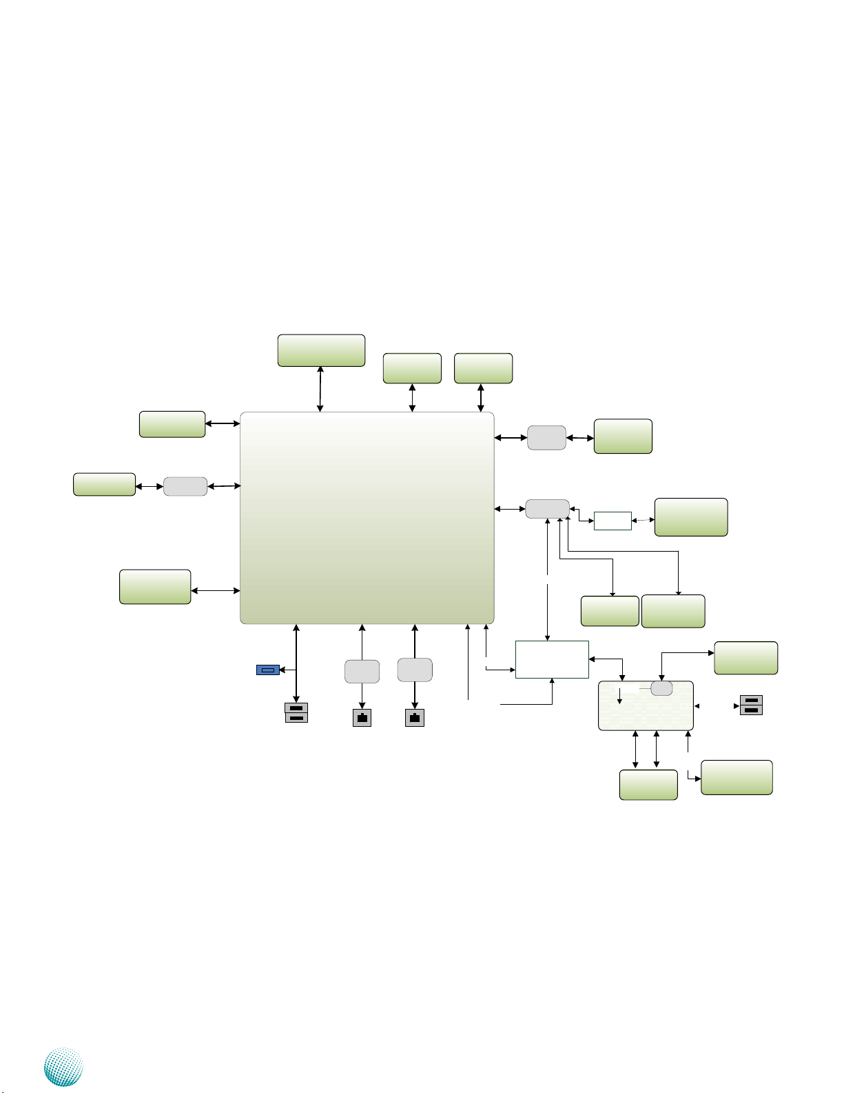
Intel® Atom™ E3825 Processor
2x PCI-E x1
1 x USB 3.0
Connector
2x USB 2.0
connectors
USB
2.0/3.0
SATA
2.0
SATA
2.0
USB 2.0
PCIe
Intel
I210
Intel
I210
SIO
DDR3L
SO-DIMM
Up to 4G
Audio
Codec
SP339E
UART X 2
MIO
Design Reservation
PCIe x 1
USB2.0 x 3
CF
SATA
Mini-PCIe with
SIM Card
Reader
Line-out
and Mic-in
Jack
DB9
RS232/422/485
x2
RS232
Pin Header
Digital I/O
DI x 2
DO x 2
VGA HDMI
SPIF223A
LEK-IOA10
DB9
RS232 x 2
2x USB 2.0
connector
USB 2.0 x2
Mini-PCIe
USB2.0
PCIe
9~30Vdc-in
PWN+12Vdc
Block Diagram
The block diagram depicts the relationships among the
interfaces and modules on the motherboard..
System Components
Embedded and Industrial Computing
7
Page 8

Chapter 2
Front Components
F1 Power-in Connector A phoenix connector for DC-in power supply;
F2
Four USB 2.0 Ports Four USB 2.0 type A connector.
F3 Reset
F4 MIC IN/LINE OUT Connect audio devices to these ports. The
F5 USB 3.0 Port
F6 Two 10/100/1000Mbps LAN ports Two RJ-45 (network) jacks with LED indicators as
LINK/ACT
System Components
F2
F1
Component Description Pin Definition
F4
F3
the system requires a 9~30V power input.
F5
F2
Reset switch
microphone and line out port are provided by
Realtek ALC
886 HD Audio.
An USB 3.0 type A connector.
described below. Both LAN ports are provided
by Intel I210. The I210 supports PXE and iSCSI
SPEED
remote boot options.
LINK/ACT (Yellow)
F6
F7
F8
F9
Reference
DCIN1 on page 17
USB1 of LEK-IOA10 on
page 17/ USB1 of LEB2530 on page 15
USB2 on page 15
LAN1/LAN2 on page
15
On/Flashing: The port is linking and active •
in data transmission.
Off: The port is not linking.•
SPEED (Green/Yellow)
Yellow: The connection speed is •
1000Mbps.
Green: The connection speed is 100Mbps•
Off: The connection speed is 10Mbps.•
F7 HDD (Yellow)
3G Status (Green) and
Power LED (Green)
F8 Power-on Switch A power-on switch through the Phoenix
F9 Power Button with dual LED ATX Power-on button with LEDs: Standby
Embedded and Industrial Computing
HDD
Blinking: data access activities•
Off: no data access activities•
3G Status
Blinking: 3G transmission activities•
On: 3G expansion card exists•
Off: no 3G expansion card exists•
Power
On: The computer is on.•
Off: The computer is off .•
PSBTN2 on page 16
contact for remote power-on/off control
8
mode in Red; Power-on mode in Green
Page 9

Chapter 2
Rear Components
System Components
R1
Component Description Pin Definition Reference
R1 HDMI The HDMI (High-Denition Multimedia Interface).
R2 VGA Port
R3 DIO Digital Input/Output Connector 2 DI and 2 DO
R4 COM1~COM4 Serial Ports COM1 and COM2 are capable of RS232/422/485
R2
R3
This port can support up to 1920x1080 resolution.
The displays can support VGA up to 1600x1200
resolution.
connections
modeswith automatic hardware flow control.
To switch among RS232/422/485, use the BIOS
menu.
COM3 and COM4 are capable of RS232 mode
only.
R4
HDMI1 on page 15
VGA1 on page 15
DIO1 on page 16
COM1/COM2 of LEB2530 on page 14
COM3/COM4 of
LEK-IOA10 on page 17
Embedded and Industrial Computing
9
Page 10

Chapter 3
Chapter 3:
Board Layout
External Connectors
The following picture highlights the location of the
external ports of the LEB-2530. Refer to the table 3.1
Connector List for more details.
Board Layout
HDMI1
VGA1
DIO1
COM1
COM2
PSBTN2
Embedded and Industrial Computing
LAN1
LAN2
USB1
USB2
LOUT1
MIC1
10
Page 11

Chapter 3
Internal Connectors and Jumpers
The following picture highlights the location of internal
connectors and pin headers of the LEB-2530. Refer to the
table 3.1 Connector List for more details.
Board Layout
JCMOS1
JLPC1
JSPI1
MPCIE1
JRI1
JRI2
JCOM1
JCOM2
Embedded and Industrial Computing
SATA1
SATAPWR1
CF1
JKBMS1
11
Page 12

Chapter 3
Internal Connectors and Jumpers
The following picture highlights the location of connectors
and jumpers of the LEK-IOA10. Refer to the table 3.2
Connector List for more details.
Board Layout
COM3
MPCIE1
COM4
Embedded and Industrial Computing
USB1
USB_SEL1
DCIN1
12
Page 13

Chapter 3
Board Layout
Connectors and Jumpers List
The tables below list the function of each of the board
jumpers and connectors by labels shown in the above
section. The next section in this chapter gives pin
definitions and instructions on setting jumpers.
Table 3.1 Connector List for LEB-2530 Board
Labels Function Pin Denition Refer-
ence Page
CF1 CompactFlash Connector P16
COM1/COM2 RS232 Serial Ports COM1 and COM2 P14
DIO1 Digital Input/Output P16
HDMI1 High-Denition Multimedia Interface Port P15
JCMOS1 Clear CMOS Jumper P15
JCOM1/2 RS232 Pin Headers P14
JKBMS1 PS/2 Keyboard & Mouse Connector P16
JLPC1 Low-pin Count Interface Reserved for Factory Use
JRI1/2 COM1/COM2 Pin 9 Signal Selection P14
JSPI1 SPI ROM Interface (for debug use only) Reserved for Factory Use
LAN1/LAN2 RJ45 Ethernet Ports P15
MPCIE1 Mini-PCIe Connectors (with SIM1) P16
PSBTN2 Power Button with Phoenix Connector P16
SATA1 Serial-ATA Connector (SATA1) P15
SATAPWR1 SATA HDD Power Connector P15
SIM1 SIM Card Reader P16
USB1 USB 2.0 Type A Dual Port P15
USB2 USB 3.0 Type A Port P15
VGA1 VGA Connector P15
Table 3.2 Connector List for LEK-IOA10 Board
Labels Function Pin Denition Refer-
ence Page
COM3/COM4 RS232 Serial Ports COM3 and COM4 P17
USB1 USB 2.0 Type A Dual Port P17
MPCIE1 Mini-PCIe Connectors (with SIM1) P17
DCIN1 DC-IN Connector P17
USB_SEL1 USB Signal Selection P17
Embedded and Industrial Computing
13
Page 14

Chapter 3
Board Layout
Jumper Settings
LEB-2530 Pin Definitions
RS-232 Pin Headers (JCOM1/2): It is a RS-232 serial
communication interface Connector
10
8
6
4
2
Pin No. Signal
1 Data Carrier Detect ( DCD # )
2 Receive Data ( RXD )
3 Transmit Data ( TXD )
4 Data Terminal Ready ( DTR # )
5 Ground ( GND )
6 Data Set Ready ( DSR # )
7 Request To Send ( RTS # )
8 Clear To Send ( CTS # )
9 Ring Indicator ( RI # )
9
7
5
3
1
2
1
RS-232
10
9
Select COM1/COM2 Pin 9 Function (JRI1/JRI2): The
pin 9 of COM1 and COM2 can be altered by JRI1 and JRI2
respectively according to the following jumper settings.
JRI1: COM1 JRI2: COM2
Default
+5V
+12V
2 4 6
1 3 5
2 4 6
2 4 6
1 3 5
6
4
2
6
4
2
6
4
2
5
3
1
5
3
1
5
3
1
RS-232/422/485 Serial Port (COM1 and COM2): It is
an RS-232/422/485 port with automatic hardware flow
control through a D-SUB9 connector.
12345
Pin No. Signal
1 Data Carrier Detect ( DCD # )
2 Receive Data ( RXD )
3 Transmit Data ( TXD )
4 Data Terminal Ready ( DTR # )
5 Ground ( GND )
6 Data Set Ready ( DSR # )
7 Request To Send ( RTS # )
8 Clear To Send ( CTS # )
9 Ring Indicator ( RI # )
Pin No. Signal
RS-422
1 TXD2 TXD+
3 RXD+
4 RXD5 GND
6789
RS-232
Pin No. Signal
RS-485
1 DATA2 DATA+
3
4
5 GND
Jumper Setting
Function
RI# (default) 1-2
+5V 3-4
+12V 5-6
SW1/SW4
Note: To switch among RS-232, 422, 485
communication protocols, use the BIOS menu.
Embedded and Industrial Computing
14
Page 15

Chapter 3
Board Layout
Clear CMOS jumper (JCMOS1): It is for clearing the CMOS
settings.
1
2
3
Pin No. Signal
1-2 Normal (Default)
2-3 Clear CMOS
VGA (VGA1)
11 12 13 14 15
1 2 3 4 5
Pin Signal Pin Signal Pin Signal
1 Red Color
Signal
2 Green Color
Signal
3 Blue Color
Signal
4 Reserved 9 +5V 14 VSYNC
5 GND 10 GND 15 DDC CLK
6 GND 11 NC
7 GND 12 DDC DATA
8 GND 13 HSYNC
HDMI Connector (HDMI1): High-Definition Multimedia
Interface Connector
19 1
18 2
Pin Signal Pin Signal
1 DATA2+ 2 GND
3 DATA2- 4 DATA1+
5 GND 6 DATA17 DATA0+ 8 GND
9 DATA0- 10 CLK+
11 GND 12 CLK13 N.C 14 N.C
15 DDC CLK 16 DDC DAT
17 GND 18 HDMI_VCC
19 HPD
Serial-ATA Connector (SATA1): It is for connecting a 2.5’’
harddisk to serve as your system’s storage. It can support
SATA II which features Data transfer rates up to 3.0 Gb/s
(300 MB/s).
Pin No. Signal
1 GND
2 TX0_P
3 TX0_N
4 GND
5 RX0_N
6 RX0_P
7 GND
SATA1
7
6
5
4
3
2
1
4-pin Serial-ATA Power Connector (SATAPWR1): It is for
connecting the SATA power cord.
1 2 3 4
Pin No. Signal
1 12V
2 GND
3 GND
4 +5V
Dual USB 2.0 Port (USB1):
1 2 3 4
5 6 7 8
Pin No. Signal
1 +5V
2 DATA3 DATA+
4 GND
5 +5V
6 DATA7 DATA+
8 GND
Single USB 3.0 Port (USB2)
Pin No. Signal
1 +5V
2 DATA3 DATA+
4 GND
5 SSRX6 SSRX+
7 GND
8 SSTX9 SSTX+
RJ45 LAN Ports (LAN1/LAN2): These LAN ports are
provided by Intel I210 to be fully compliant to IEEE802.3
Ehternet interface for 10BASE-T/100BASE-TX/1000BASE-T.
It also supports IEEE 802.1Qav Audio-Video Bridging (AVB)
and IEEE 802.3za EEE standards.
Pin No. Signal
1 MDI0+
2 MDI03 MDI1+
4 MDI2+
5 MDI26 MDI17 MDI3+
8 MDI3-
Embedded and Industrial Computing
15
Page 16

Chapter 3
Board Layout
Power-on Switch through Phoenix Contact (PSBTN2):
A Phoenix connector for distant power switch.
1 2
Pin No. Signal
1 PWRBTN#
2 GND
Digital Input/Output Connector (DIO1)
2 6
1 5
Pin NO. Signal Pin NO. Signal
1 DIO_IN1 2 DIO_IN2
3 DIO_OUT1 4 DIO_OUT2
5 +5V 6 GND
Maximum input/output current for each port is
10mA/100mA
For all Input/
output pins:
Voltage Logic Register
DI: < 0.8V
Low 0
Do: <0.4V
DI: >3.5V
High 1
Do: 5V
The default BIOS value is DI=0, DO=1
Mini PCI Express Connector (for 3G card with PCI
Express 1X and USB 2.0 signals and a SIM card reader,
MPCIE1):
PIN Signal PIN Signal
1 WAKE# 2 +3.3Vaux
3 COEX1 4 GND
5 COEX2 6 +1.5V
7 CLKREQ# 8 UIM_PWR
9 GND 10 UIM_DATA
11 REFCLK+ 12 UIM_CLK
13 REFCLK- 14 UIM_RESET
15 GND 16 UIM_VPP
Key
17 RSVD 18 GND
19 RSVD 20 W_DISABLE#
21 GND 22 PERST#
23 PERn0 24 +3.3Vaux
25 PERp0 26 GND
27 GND 28 +1.5V
29 GND 30 SMB_CLK
31 PETn0 32 SMB_DATA
33 PETp0 34 GND
35 GND 36 USB_D37 GND 38 USB_D+
39 +3.3Vaux 40 GND
41 +3.3Vaux 42 LED_WWAN#
43 GND 44 LED_WLAN#
45 RSVD 46 LED_WPAN#
47 RSVD 48 +1.5V
49 RSVD 50 GND
51 RSVD 52 +3.3Vaux
PS/2 Keyboard and Mouse Connector (JKBMS1)
1
3
5
7
Pin NO. Description Pin NO. Description
1 VCC 2 MSCLK
3 MSDATA 4 KEY
5 KBDATA 6 KEY
7 GND 8 KBCLK
2
4
6
8
SIM Card Reader (SIM1)
C5
C7
Pin NO. Signal Pin NO. Signal
C1 UIM_PWR C5 GND
C2 UIM_RST# C6 UIM_VPP
C3 UIM_CLK C7 UIM_DATA
C1
C3
CF Connector (CF1)
Pin No. Signal Pin No. Signal
1 GND 26 -CD1
2 D3 27 D11
3 D4 28 D12
4 D5 29 D13
5 D6 30 D14
6 D7 31 D15
7 -CS0 32 -CS1
8 A10 (GND) 33 -VS1
9 ATA_SEL# 34 -IORD
10 A9 (GND) 35 -IOWR
11 A8 (GND) 36 -WE
12 A7 (GND) 37 INTRQ
13 VCC 38 VCC
14 A6 (GND) 39 -CSEL
15 A5 (GND) 40 -VS2
16 A4 (GND) 41 -RESET
17 A3 (GND) 42 IORDY
18 A2 43 DMARQ
19 A1 44 -DDACK
20 A0 45 -DASP
21 D0 46 -PDIAG
22 D1 47 D8
23 D2 48 D9
24 -IOCS16 49 D10
25 -CD2 50 GND
Embedded and Industrial Computing
16
Page 17

Chapter 3
Board Layout
LEK-IOA10 Pin Definitions
RS-232 Serial Port (COM3 and COM4): It is an RS-232
serial port through a D-SUB9 connector.
12345
6789
Pin No. Signal
RS-232
1 Data Carrier Detect ( DCD # )
2 Receive Data ( RXD )
3 Transmit Data ( TXD )
4 Data Terminal Ready ( DTR # )
5 Ground ( GND )
6 Data Set Ready ( DSR # )
7 Request To Send ( RTS # )
8 Clear To Send ( CTS # )
9 Ring Indicator ( RI # )
Dual USB 2.0 Port (USB1):
Pin No. Signal
1 +5V
2 DATA3 DATA+
4 GND
5 SSRX6 SSRX+
7 GND
8 SSTX9 SSTX+
Mini PCI Express Connector (for cards with PCI Express 1X and USB 2.0 signals, MPCIE1):
PIN Signal PIN Signal
1 WAKE# 2 +3.3Vaux
3 COEX1 4 GND
5 COEX2 6 +1.5V
7 CLKREQ# 8 UIM_PWR
9 GND 10 UIM_DATA
11 REFCLK- 12 UIM_CLK
13 REFCLK+ 14 UIM_RESET
15 GND 16 UIM_VPP
Key
17 RSVD 18 GND
19 RSVD 20 W_DISABLE#
21 GND 22 PERST#
23 PERn0 24 +3.3Vaux
25 PERp0 26 GND
27 GND 28 +1.5V
29 GND 30 SMB_CLK
31 PETn0 32 SMB_DATA
33 PETp0 34 GND
35 GND 36 USB_D37 GND 38 USB_D+
39 +3.3Vaux 40 GND
41 +3.3Vaux 42 LED_WWAN#
43 GND 44 LED_WLAN#
45 RSVD 46 LED_WPAN#
47 RSVD 48 +1.5V
49 RSVD 50 GND
51 RSVD 52 +3.3Vaux
DC_IN CONNECTOR (DCIN1): A Phoenix connector for
external power supply.
1 2
Pin No. Pin Name
1 GND
2 DC_VIN
USB Signal Selection (USB_SEL1)
1
2
3
4
Pin No. Pin Name
1-5,2-6,3-7,4-8 (Default) For use with the LEB-7230 board only;
5-9,6-10,7-11,8-12 For other uses; the MPCIE1connector
Embedded and Industrial Computing
9
10
11
12
the MPCIE1 connector supports both
PCIe and USB signals.
supports PCIe signal only
17
Page 18

Chapter 4
Chapter 4:
Hardware Setup
Preparing the Hardware Installation
Hardware Setup
1
To access some components and perform certain service
procedures, you must perform the following procedures
first.
WARNING: To reduce the risk of personal injury,
electric shock, or damage to the equipment,
remove the power cord to remove power from
the server. The power switch button does not
completely shut off system power. Portions of the
power supply and some internal circuitry remain
active until power is removed.
Unpower the LEC-2530 and remove the power cord.1.
Turn the device upside down.2.
Unscrew the 4 rubber feet from the bottom cover.3.
Open the cover.4.
2
Note:
The system can support memory of DDR3L SODIMM up to 4 GB in maximum.
Installing the System Memory
The motherboard supports DDR3 memory to meet the
higher bandwidth requirements of the latest operating
system and Internet applications. It comes with one LowVoltage Double Data Rate Three (DDR3L) Small Outline
Dual Inline Memory Module (SO-DIMM) socket.
Align the memory module’s key with the SO-DIMM 1.
socket’s notch.
Install the SO-DIMM.2.
Embedded and Industrial Computing
18
Page 19

Chapter 4
Hardware Setup
Installing the Wireless Module
Align the wireless module’s key with the Mini-PCIe slot 1.
notch.
Insert the wireless module into the connector 2.
diagonally.
Fix the wireless module with the screws.3.
Installing the 3G SIM Card
Unlock the SIM card reader first by sliding it outward.1.
Flip the SIM card reader diagonally.2.
Put the SIM card into the reader. The angled corner of 3.
the SIM ensures that the card fits only the correct way
in the reader. Make sure the ICs will be in contact with
the SIM card reader.
C4. lose the tray. You should feel a click when the SIM
card is locked securely in the SIM card reader.
Installing the Hard Disk
The system can accommodate one Serial-ATA disk. Follow
these steps to install a hard disk into the system:
Align the mounting holes of the HDD and that on 1.
the LEC-2530 systems as illustrated in the following
picture. Fix the hard disk on the system by attaching
the screws through the back cover from the outside.
Plug the Serial-ATA cable to the hard disk.2.
Connect the Serial-ATA power and data disk cables to 3.
the Serial-ATA power and disk connectors on the main
board respectively.
Lock
Unlock
2
3
Embedded and Industrial Computing
19
Page 20

Chapter 4
Hardware Setup
Installing the CompactFlash Card
LEC-2530 provides one CompactFlash slot. Follow the
procedures bellow for installing a CompactFlash card.
Align CompactFlash card and the card slot with the 1.
arrow pointing toward the connector.
Push the card to insert into the connector.2.
1
Embedded and Industrial Computing
20
Page 21

Appendix C
Terms and Conditions
Appendix C:
Terms and Conditions
Warranty Policy
All products are under warranty against defects in 1.
materials and workmanship for a period of one year
from the date of purchase.
The buyer will bear the return freight charges for 2.
goods returned for repair within the warranty period;
whereas the manufacturer will bear the after service
freight charges for goods returned to the user.
The buyer will pay for repair (for replaced components 3.
plus service time) and transportation charges (both
ways) for items after the expiration of the warranty
period.
If the RMA Service Request Form does not meet the 4.
stated requirement as listed on “RMA Service,” RMA
goods will be returned at customer’s expense.
The following conditions are excluded from this 5.
warranty:
RMA Service
Requesting a RMA#
To obtain a RMA number, simply fill out and fax the 6.
“RMA Request Form” to your supplier.
The customer is required to fill out the problem code 7.
as listed. If your problem is not among the codes listed,
please write the symptom description in the remarks
box.
Ship the defective unit(s) on freight prepaid terms. 8.
Use the original packing materials when possible.
Mark the RMA# clearly on the box. 9.
Note: Customer is responsible for shipping
damage(s) resulting from inadequate/loose
packing of the defective unit(s). All RMA# are valid
for 30 days only; RMA goods received after the
effective RMA# period will be rejected.
Improper or inadequate maintenance by the customer
Unauthorized modification, misuse, or reversed
engineering of the product Operation outside of the
environmental specifications for the product.
Embedded and Industrial Computing
21
Page 22

Appendix C
RMA Service Request Form
When requesting RMA service, please fill out the following form. Without
this form enclosed, your RMA cannot be processed.
RMA No:
Reasons to Return: Ŀ Repair(Please include failure details)
Ŀ Testing Purpose
Company: Contact Person:
Phone No. Purchased Date:
Fax No.: Applied Date:
Return Shipping Address:
Shipping by: Ŀ Air Freight Ŀ Sea Ŀ Express ___
Ŀ Others:________________
Item Model Name Serial Number Configuration
Item Problem Code Failure Status
*Problem Code:
01:D.O.A.
02: Second Time
R.M.A.
03: CMOS Data Lost
04: FDC Fail
05: HDC Fail
06: Bad Slot
07: BIOS Problem
08: Keyboard Controller Fail
09: Cache RMA Problem
10: Memory Socket Bad
11: Hang Up Software
12: Out Look Damage
13: SCSI
14: LPT Port
15: PS2
16: LAN
17: COM Port
18: Watchdog Timer
19: DIO
20: Buzzer
21: Shut Down
22: Panel Fail
23: CRT Fail
24: Others (Pls specify)
Request Party
Confirmed By Supplier
Authorized Signature / Date Authorized Signature / Date
Terms and Conditions
Embedded and Industrial Computing
22
 Loading...