

Page 1

>>
Embedded &
Industrial Computing
Hardware Platforms for Embedded and Industrial Computing
LEC-2280
Preliminary
User's Manual
Publication date:2013-02-27
Page 2
2
About
About
Embedded and Industrial Computing
Overview
Icon Descriptions
The icons are used in the manual to serve as an indication
of interest topics or important messages. Below is a
description of these icons:
NOTE: This check mark indicates that
there is a note of interest and is something
that you should pay special attention to
while using the product.
WARNING: This exclamation point
indicates that there is a caution or
warning and it is something that could
damage your property or product.
Online Resources
The listed websites are links to the on-line product
information and technical support.
Resource Website
Lanner http://www.lannerinc.com
Product Resources http://assist.lannerinc.com
RMA http://eRMA.lannerinc.com
Copyright and Trademarks
This document is copyrighted ©2013. All rights are
reserved. The original manufacturer reserves the right to
make improvements to the products described in this
manual at any time without notice.
No part of this manual may be reproduced, copied,
translated or transmitted in any form or by any means
without the prior written permission of the original
manufacturer. Information provided in this manual is
intended to be accurate and reliable. However, the original
manufacturer assumes no responsibility for its use, nor for
any infringements upon the rights of third parties that
may result from such use.
Acknowledgement
Intel, Pentium and Celeron are registered trademarks of
Intel Corp.
Microsoft Windows and MS-DOS are registered trademarks
of Microsoft Corp.
All other product names or trademarks are properties of
their respective owners.
Compliances and Certification
CE Certication
This product has passed the CE test for environmental
specifications. Test conditions for passing included the
equipment being operated within an industrial enclosure.
In order to protect the product from being damaged by
ESD (Electrostatic Discharge) and EMI leakage, we strongly
recommend the use of CE-compliant industrial enclosure
products.
FCC Class A Certication
This equipment has been tested and found to comply
with the limits for a Class A digital device, pursuant to Part
15 of the FCC Rules. These limits are designed to provide
reasonable protection against harmful interference when
the equipment is operated in a commercial environment.
This equipment generates, uses and can radiate radio
frequency energy and, if not installed and used in
accordance with the instruction manual, may cause
harmful interference to radio communications. Operation
of this equipment in a residential area is likely to cause
harmful interference in which case the user will be required
to correct the interference at his own expense.
Page 3

TTaTTable of Contentsbeable of Contents
3
Chapter 1: Introduction 3
System Specication . . . . . . . . . . . . . . . . . . . . . . . . . . . . . . . . . . . . . . . . . . . 3
Package Contents . . . . . . . . . . . . . . . . . . . . . . . . . . . . . . . . . . . . . . . . . . . . . 4
Optional Accessories . . . . . . . . . . . . . . . . . . . . . . . . . . . . . . . . . . . . . . . . . . . 4
Chapter 2: System Components 5
System Drawing . . . . . . . . . . . . . . . . . . . . . . . . . . . . . . . . . . . . . . . . . . . . . . 5
System Drawing (Continued) . . . . . . . . . . . . . . . . . . . . . . . . . . . . . . . . . . . . . . 6
Block Diagram . . . . . . . . . . . . . . . . . . . . . . . . . . . . . . . . . . . . . . . . . . . . . . . 7
Front Components. . . . . . . . . . . . . . . . . . . . . . . . . . . . . . . . . . . . . . . . . . . . . 8
Rear Components . . . . . . . . . . . . . . . . . . . . . . . . . . . . . . . . . . . . . . . . . . . . . 9
Chapter 3: Board Layout 10
Connectors . . . . . . . . . . . . . . . . . . . . . . . . . . . . . . . . . . . . . . . . . . . . . . . . .10
External Connectors. . . . . . . . . . . . . . . . . . . . . . . . . . . . . . . . . . . . . . . . . . . .11
Internal Connectors and Jumpers . . . . . . . . . . . . . . . . . . . . . . . . . . . . . . . . . . .12
Internal Connectors and Jumpers (backside) . . . . . . . . . . . . . . . . . . . . . . . . . . . .13
Connectors and Jumpers List. . . . . . . . . . . . . . . . . . . . . . . . . . . . . . . . . . . . . .14
Jumper Settings . . . . . . . . . . . . . . . . . . . . . . . . . . . . . . . . . . . . . . . . . . . . . .15
Chapter 4: Hardware Setup 21
Preparing the Hardware Installation. . . . . . . . . . . . . . . . . . . . . . . . . . . . . . . . . .21
Installing the System Memory . . . . . . . . . . . . . . . . . . . . . . . . . . . . . . . . . . . . .21
Wireless Module Installation . . . . . . . . . . . . . . . . . . . . . . . . . . . . . . . . . . . . . .22
3G SIM Card Installation . . . . . . . . . . . . . . . . . . . . . . . . . . . . . . . . . . . . . . . . .22
PCI/PCIe Riser Card Installation . . . . . . . . . . . . . . . . . . . . . . . . . . . . . . . . . . . . .22
On 2280E with one PCIe slot. . . . . . . . . . . . . . . . . . . . . . . . . . . . . . . . . . . .22
Installing the Hard Disk . . . . . . . . . . . . . . . . . . . . . . . . . . . . . . . . . . . . . . . . . .23
On 2280P2 with 2 PCI slot . . . . . . . . . . . . . . . . . . . . . . . . . . . . . . . . . . . . .23
Connecting Power . . . . . . . . . . . . . . . . . . . . . . . . . . . . . . . . . . . . . . . . . . . . .24
Wall Mounting . . . . . . . . . . . . . . . . . . . . . . . . . . . . . . . . . . . . . . . . . . . . . . .24
Appendix A: Programming Watchdog Timer 25
Appendix G: Terms and Conditions 31
Warranty Policy . . . . . . . . . . . . . . . . . . . . . . . . . . . . . . . . . . . . . . . . . . . .31
RMA Service . . . . . . . . . . . . . . . . . . . . . . . . . . . . . . . . . . . . . . . . . . . . . .31
Page 4
4
Introduction
Chapter 1
Embedded and Industrial Computing
Chapter 1:
Introduction
Thank you for choosing the LEC-2280. The LEC-2280 is
an upgrade platform of Lanner LEC-2280 and features
Intel Ivy Bridge i3, i5, and i7 processors. It has dual LAN
as well as HDMI and DVI-D connectors for high demand
of Internet and video playback applications. The LEC-2280
also features slim and compact chassis design to allow
heat to dissipate off directly from the top of the platform.
The LEC-2280 also offers a variety of different expansion
opportunities to further customize the platform. Two
different expansions are possible.
On model LEC-2280E, it comes with one PCIe.
On model LEC-2280P2, it comes with 2 PCI slots.
These expansions adds capabilities of video capture or
extended LAN connections.
The following highlight the functionalities of the LEC2280 system:
Intel HD Graphics Engine •
Dual video output of VGA and HDMI or VGA and DVI-D •
with Intel integrated HD graphic engine
Dual 10/100/1000 Mbps LAN •
USB x 6 (2 by internal pin header) and COM x 2 •
1 SATA 6Gbps HDD bay support and 1 SATA-DOM •
connector
Totally 2 serial ports supporting Hardware Auto flow •
Control: DB9 x2 for RS232/422/485
Audio input and output through Mic-in and Line-out •
jack
Dual Mini-PCIe Socket (with on SIM card reader for 3G •
wireless Internet connection) can extend the capability
for Wi-Fi or Bluetooth
Aluminum extrusion enclosure which helps heat •
dissipation
Customization opportunity for expansion of extra LAN •
and serial port (board LEK-IOA5) or eSATA and DI/DO
(LEK-IOA3)
System Specification
Dimensions (WxHxD)
277x(67/89)x194mm
(10.91”x(2.64/3.50)”x7.64”)
Processor
i5-3610ME/i3-3120ME (Ivy Bridge),
i7-3612QE, i7-3555LE
Chipset
Intel HM65
System
Memory
Technology DDR3 SO-DIMM x2
Max. Capacity Up to 16GB
Storage
IDE N/A
SATA
2.5” SSD/HDD drive bay x1, SATA-DOM
x1
Ethernet Controller
Intel 82574L x2
Graphic Controller
Intel integrated HD graphic engine
Audio Controller
ALC886
IO
LAN RJ45 10/100/1000Mbps x2
Display
Dual Display
HDMI x1 , DVI-D x1 , VGA x1
VGA+HDMI, VGA+DVI
Dual Display Mode Clone, Independent, Extend
Audio Phone Jack x2 for Mic-In and Line-Out
Serial I/O DB9 x2 for RS232./422/485
Digital I/O
DB9 Female x1 for DI x4 &DO x4 (TTL,
DO Max 100ma) - optional
USB 2.0 Type A x6
Power Input Terminal Block 2-pin
Expansion
Mini-PCIe x1 with SIM card reader
Mini-PCIe x1
PCI x 2 or PCIe (x1) x 1
Power Input
+9~+30v Input, Support ATX Function
Hardware Monitor
Fintek F81865 integrated
Watchdog Timer 1~255 level
OS Support
Win7/XP/7Embedded/XP Embed-
ded, Redhat Enterprise 5/Fedora
14, Linux Kernel 2.6.18 or Later
Certications
CE, FCC Class A
Operating
Temperature
Range
With Industrial
Components
-10 to +45°C/14~113°F for processor
power consumption of 35W
-10 to +50°C/14~122°F for processor
power consumption below 25W
With Commercial
Components
-5~45°C / 23~113°F
High/Low Extended Temperature
Tested
Bootable after 24 hours @ -40°C
Ordering Information
LEC-2280E
Intel i5/i7/Celeron on-board CPU,
2 DDR3 SO-DIMM Sockets,
2 COM Ports,
1 HDMI, 1 DVI-D, 1 VGA, Audio Ports
2 LAN Ports, DIO (4 in, 4 out) – optional
+9~30V DC input support with one PCIe expansion
LEC-2280P2
Intel i5/i7/Celeron on-board CPU,
2 DDR3 SO-DIMM Sockets,
2 COM Ports,
1 HDMI, 1 DVI-D, 1 VGA, Audio Ports
2 LAN Ports, DIO (4 in, 4 out) – optional
+9~30V DC input support with two PCI expansion
Page 5

5
Introduction
Chapter 1
Embedded and Industrial Computing
Package Contents
Your package contains the following items:
LEC-2280 Fanless Embedded System •
Serial-ATA/Power Cable (P/N: 080W1N0002001) •
Wall-Mounting Kit (P/N: SE9ESA900R100) •
Drivers and User’s Manual CD (087W0200V1001) •
Power Adapter (P/N: 0P0W075190001) •
Optional Accessories
The system has a variety of optional accessories including
the power cords and Wi-Fi or 3G modules for extended
capabilities. For details of these modules, visit:
http://www.lannerinc.com/Embedded_Computing/LEC2280
Page 6
6
System Components
Chapter 2
Embedded and Industrial Computing
Chapter 2:
System Components
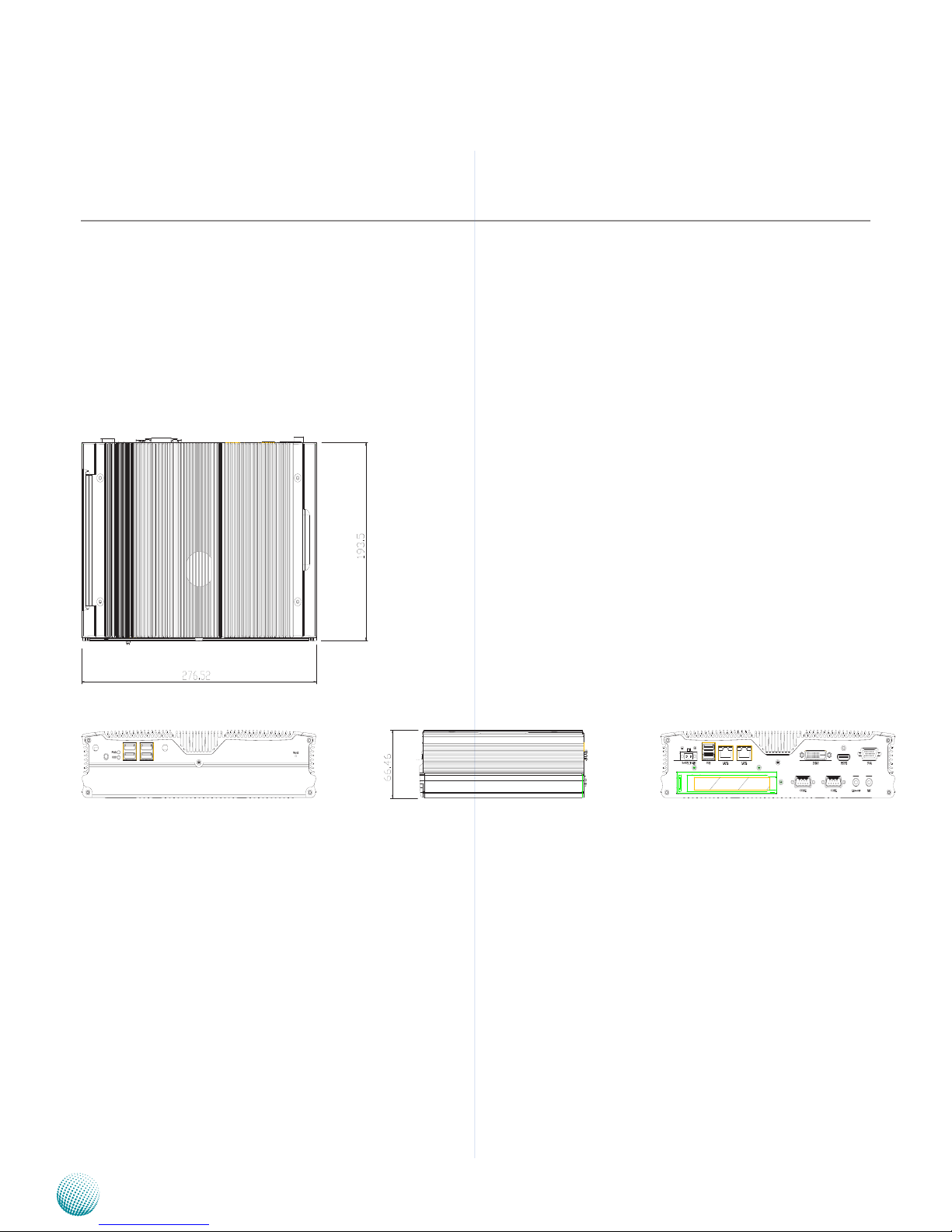
System Drawing
Mechanical dimensions of the LEC-2280E
Unit: mm
Page 7
7
System Components
Chapter 2
Embedded and Industrial Computing
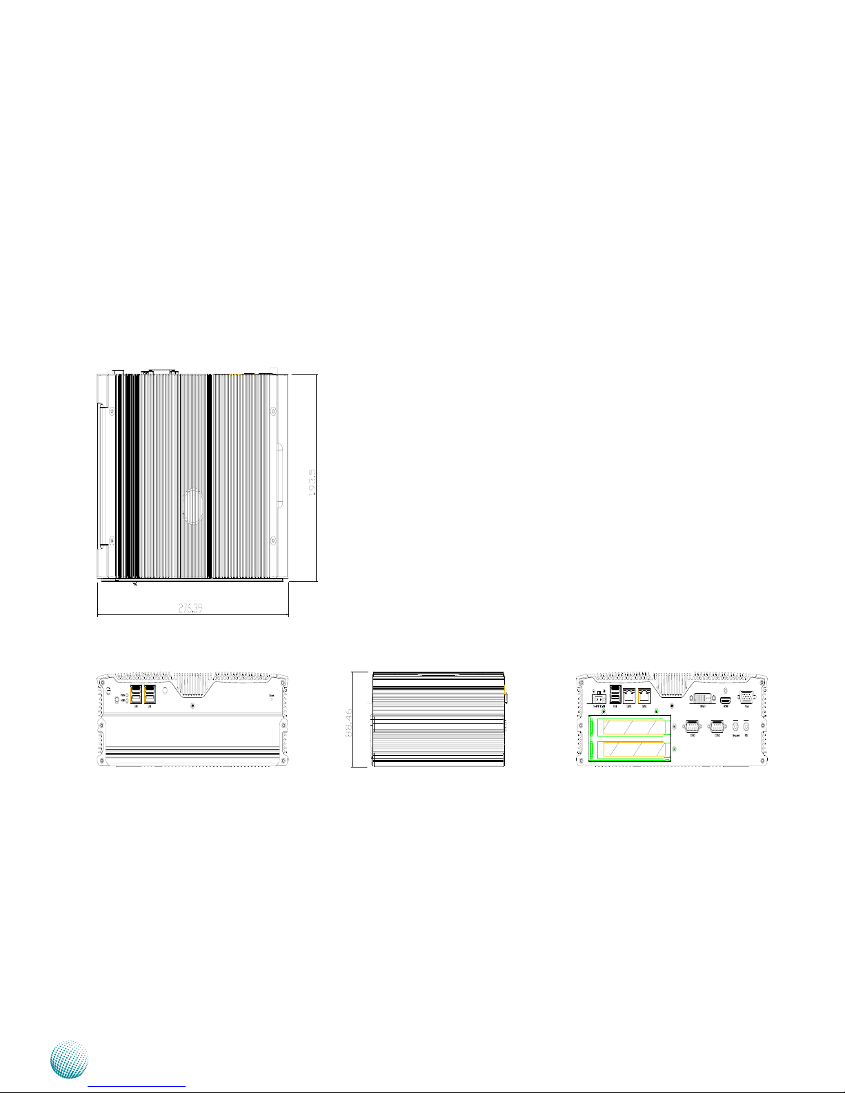
System Drawing (Continued)
Mechanical dimensions of the LEC-2280P2
Unit: mm
Page 8
8
System Components
Chapter 2
Embedded and Industrial Computing
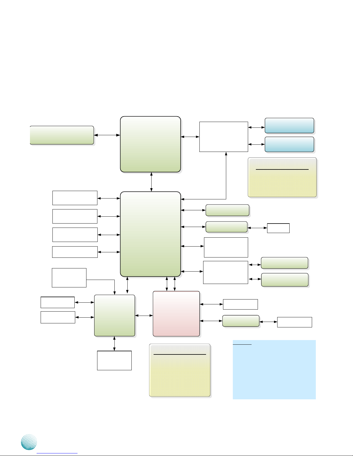
Block Diagram
The block diagram depicts the relationships among the
interfaces and modules on the motherboard..
PCH
HM65
Processor
Intel
IVY Bridge series
(BGA)
DMI2 x4
DDR3 1066/1333/1600
2x SO-DIMM up to 16GB
Fintek
F81865F
H/W Monitor
WDT
RS-232/422/485
2x DB-9
P/S2 KB/MS
Pin Header
SATA Port 0
SATA Port 1
USB
Flash BIOS
SPI
Mini PCI Express
2x Socket
Wifi Card
GbE LAN
Intel 82574L
2x PCIe
2x RJ-45
USB 2.0
4x Port-A (front I/O)
2x Port-A (rear I/O)
2x Pin Header
SATA Connector
2x 6 Gbps
PCIe x2
USB x2
VGA
Up to 2048x1536
DVI-D
Up to 1920x1200
Port C
HDMI
Up to 1920x1200
Port D
3G Card +
SIM Card Reader
LPC
PCIe Expansion
For Riser Board (pin header)
PEG
LEK-IOA2
audio & serial board
Serial
Intel HD
Audio In/Out
1/8 Phone Jack
Audio Codec
ALC 886
LEK-EA2*
PCIe x1 Slot
LEK-PB2*
2x PCI Slots
Voltage
Thermal
Sensor
2x PCIe !x
USB x2
Multi I/O Function
UART X4
Digital I/O x4
USB x2
PCIe x2
HD Audio
SATA x1
3.3V/5V/V1.5V/12V
PCIe I/O Function
PCI-Express 16X *1
PCI-Express 1X *2
PCI-E CLOCK *3
3.3V /3.3V
SB
/5V/12V
IR remote
Receiver
(Optional)
Remark*
The expansion gold finger is flexible for
PCI and PCIe 1X signals (please refers to
"PCIe I/O Function" block);
For LEC-2280, the daughter board
LEK-EA2 or LEK-PB2 are selected by
different SKUs.
* LEK-EA2 is for LEC-2280E
* LEK-PB2 is for LEC-2280P2
Page 9

9
System Components
Chapter 2
Embedded and Industrial Computing
Front Components
Component Description Pin Definition Reference
F1 Power Button with dual LED ATX Power-on button with LEDs:
Standby mode in Red; Power-on mode
in Green
F2 HDD (Yellow) and
Power LED (Green)
HDD
Blinking: data access activities•
Off: no data access activities•
Power
On: The computer is on.•
Off: The computer is off .•
F3 Four USB 2.0 Ports An USB type A connector. In addi-•
tion to this connector, an internal
pin header is also provided.
USB1, USB2 on Page 18
F4 Reset Reset switch RST1 on page 20
F1
F2
F3
F4
Page 10
10
System Components
Chapter 2
Embedded and Industrial Computing
Rear Components
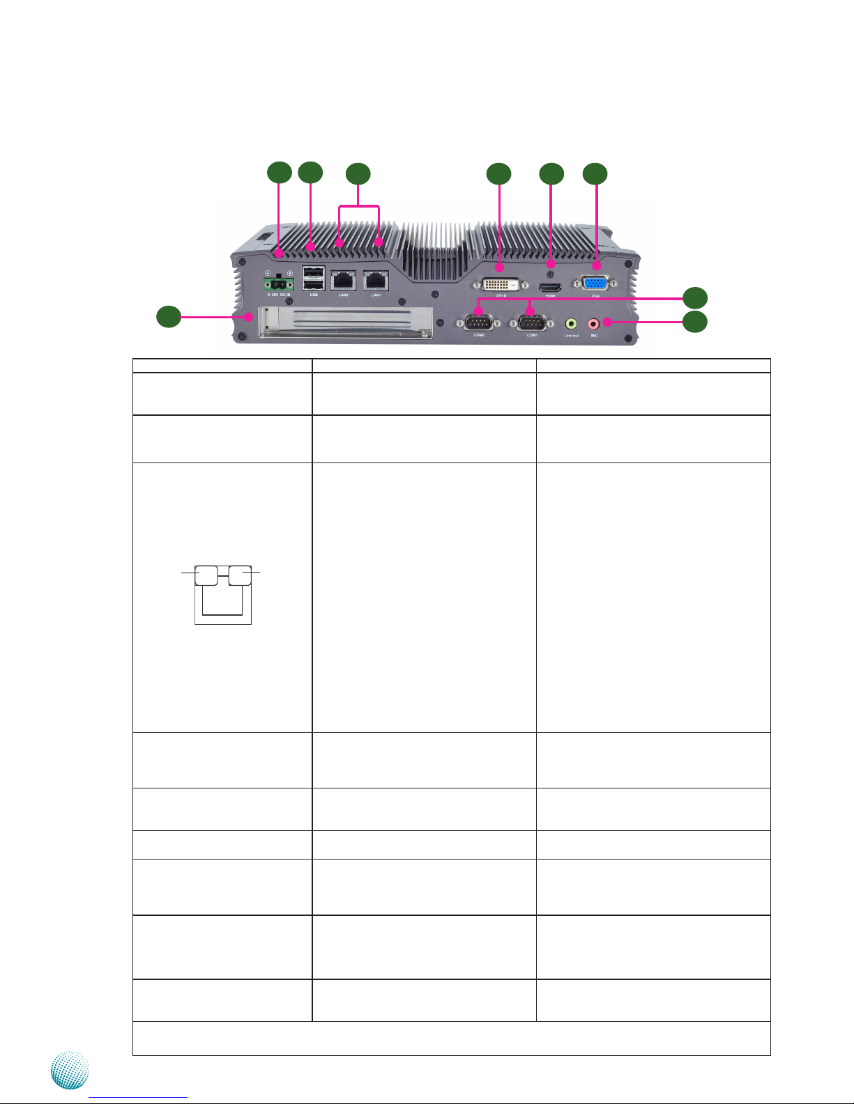
Component Description Pin Definition Reference
R1 DC-In (power) 1x2 Pin
Phoenix Contact Connector
Power-in Connector. The LEC-2280
support power range between
+9~+30V DC-in.
CN4 on page 20
R2 Two USB 2.0 Ports An USB type A connector. In addition to
this connector, an internal pin header is
also provided..
USB3 Connector on Page 18
R3 Two 10/100/1000Mbps LAN
ports
Two RJ-45 (network) jacks with LED
indicators as described below. The LAN
ports are provided by Intel 82574L.
They both support WOL/Remotewake-up/PXE function.
LINK/ACT (Yellow)
On/Flashing: The port is linking •
and active in data transmission.
Off: The port is not linking.•
SPEED (Green/Amber)
Amber: The connection speed is •
1000Mbps.
Green: The connection speed is •
100Mbps
Off: .The connection speed is •
10Mbps.
LAN1/LAN2 on page 21
R4 DVI-D A DVI-D port (single link) which is
provided by Intel HD Graphic Engine.
This port can support up to 1920x1200
@ 60 Hz resolution.
DVID1 Connectors on page 19
R5 HDMI A HDMI (High-Definition Multimedia
Interface).This port can support up to
1920x1200 @ 60 Hz resolution.
HDMI1 on page 19
R6 VGA Port(†) The displays can support VGA up to
2048x1536 resolution.
VGA1 on page 17
R7 MIC IN/LINE OUT(†) Connect the audio devices to these
ports. The Microphone and line out
port are provided by Realtek ALC
ALC886.
CN1, CN2 on page 16
F8 Serial Ports Serial ports through the DB-9
connector; Both COM1 and COM2
support RS-232/422/485 with jumper
selection among RS-232/422/485.
COM1/COM2 on page 16
R9 Slot for PCIe expansion (*) The PCIe/PCI expansion capability
is accomplished via the riser card
connected to the system
PCIEIO1 Connector on page 19
†Note that the driver for these ports should be installed with the following order: Chipset INF->Graphic->Audio
* Model LEC-2280P2 can support 2 PCI expansion.
R9
R2
R6
R1
SPEED
LINK/ACT
R3 R5
R4
R7
R8
Page 11
11
Board Layout
Chapter 3
Embedded and Industrial Computing
Chapter 3:
Board Layout
Connectors
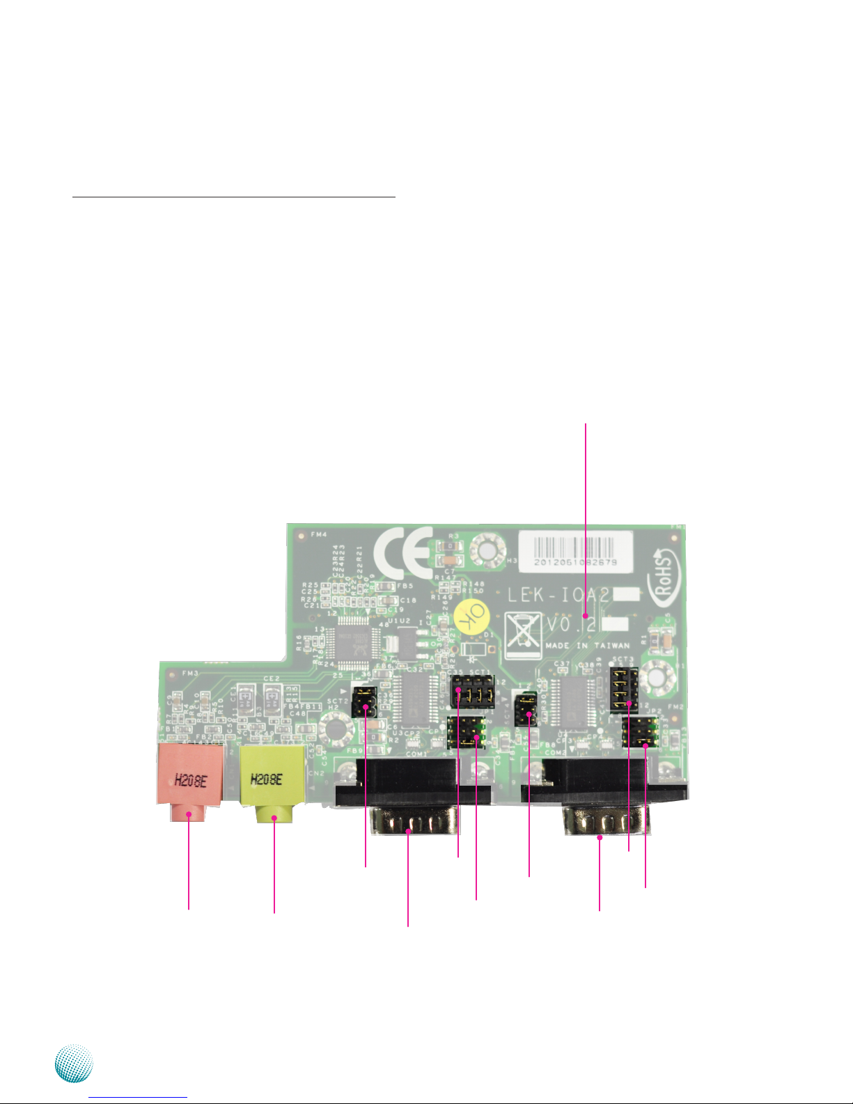
The following picture highlights the location of the COM
port and audio expansion card. Refer to the table 3.1
Connector List for more details.
Note: Daughter boards such as COM ports and
low-profile PCIe extension boards can only be
inserted to the mainboards with the same version.
Failure to do so may damage the system. The
board version is shown on top of the boards.
COM1
COM2
CN1
CN2
SCT2
SCT1
JP1
SCT4
SCT3
JP2
LEK-IOA2
Board Version
Page 12
12
Board Layout
Chapter 3
Embedded and Industrial Computing
External Connectors
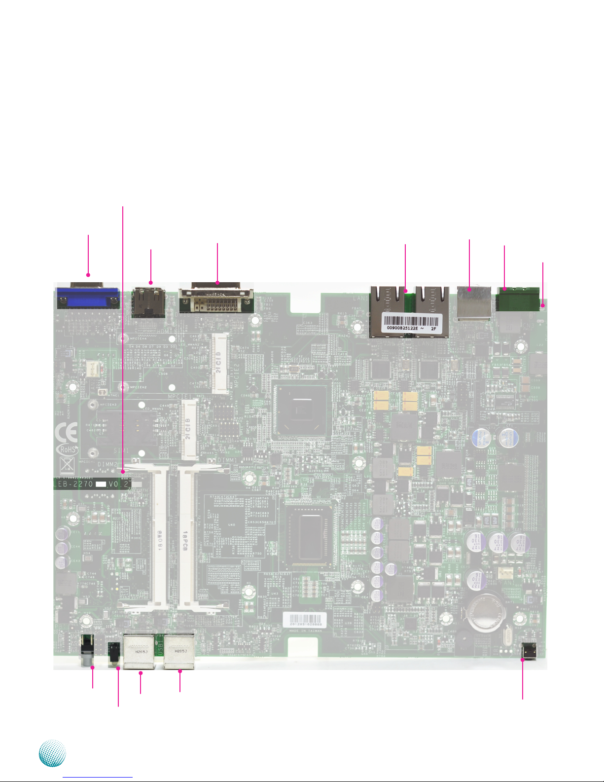
The following picture highlights the location of system
input/output connectors. Refer to the table 3.2 Connector
List for more details.
DVID1
USB1
LAN1/LAN2
HDMI1
USB3
USB2
RST1
VGA1
CN4
POWER1
LED1
LEB-2280
CN3/
DCJK1
(optional)
Board Version
Page 13
13
Board Layout
Chapter 3
Embedded and Industrial Computing
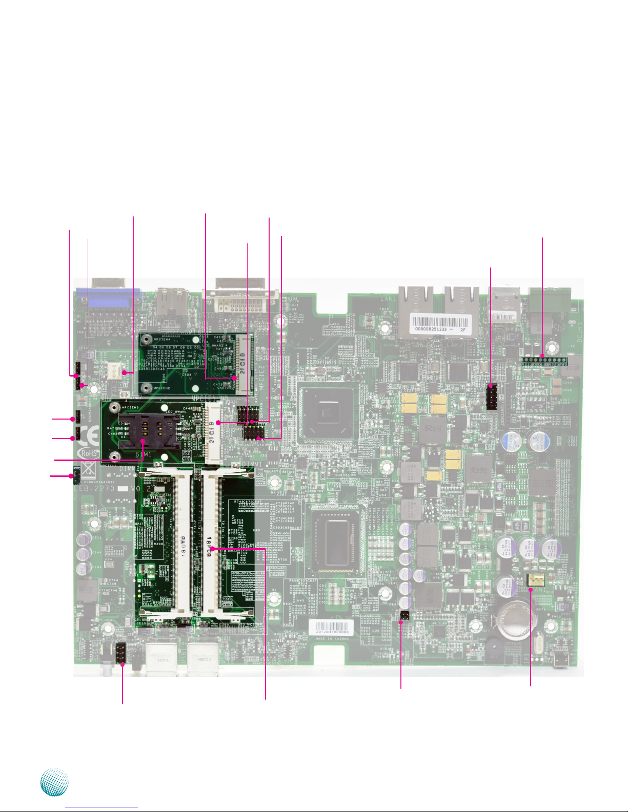
Internal Connectors and Jumpers
The following picture highlights the location of internal
connectors and jumpers. Refer to the table 3.2 Connector
List for more details.
LPC1
LEB-2280
MPCIE1
FAN2
USB4
SIM1
SO-DIMM
SPI1
FRONT1
CMOS2
J1
MPCIE2
FAN1
CMOS1
SATA_PW2
Ignition1
COMSLT2
COMSLT1
Page 14
14
Board Layout
Chapter 3
Embedded and Industrial Computing
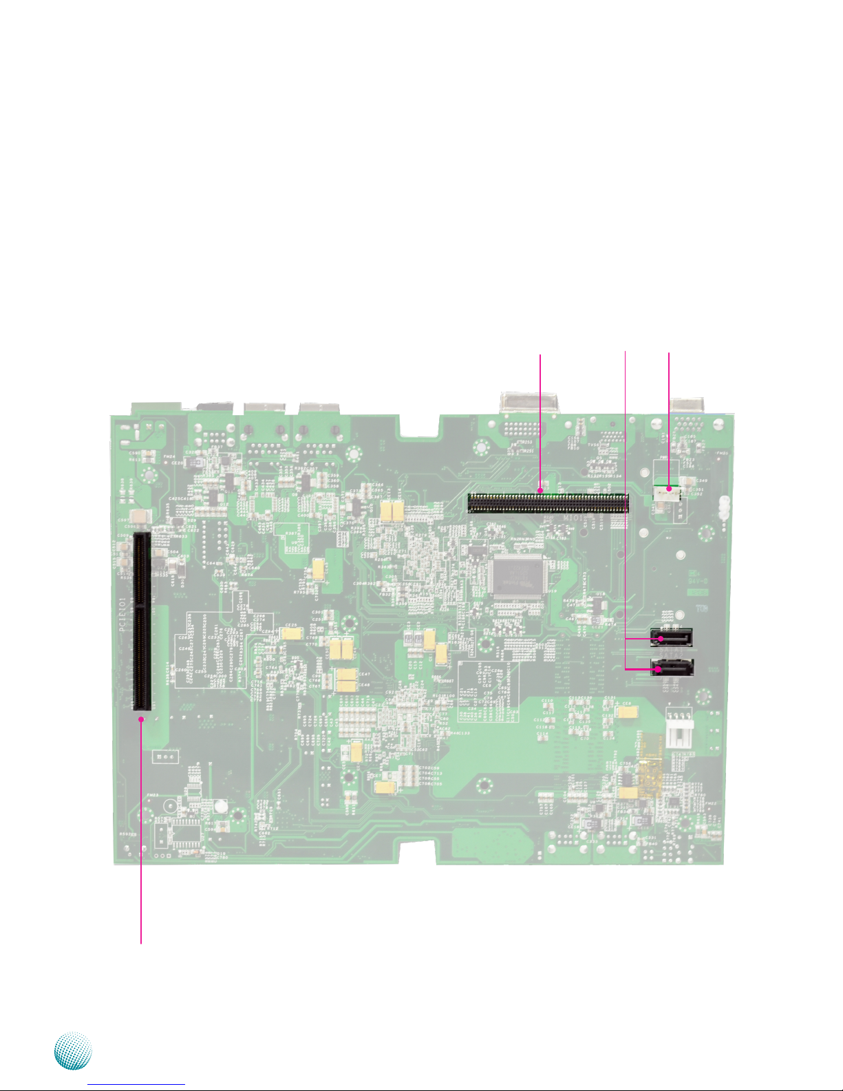
Internal Connectors and Jumpers
(backside)
The following picture highlights the location of internal
connectors and jumpers on the backside of the board.
Refer to the table 3.2 Connector List for more details.
SATA1
SATA2
PCIEIO1
PWR1
MIO1
LEB-2280
Page 15
15
Board Layout
Chapter 3
Embedded and Industrial Computing
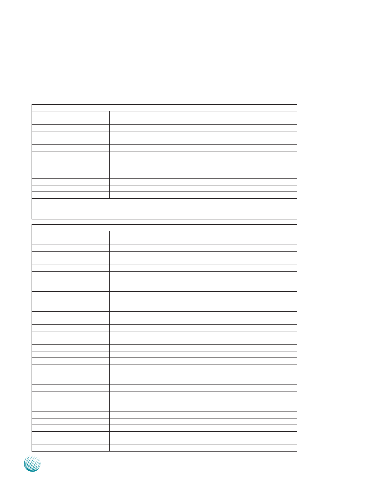
Connectors and Jumpers List
The tables below list the function of each of the board
jumpers and connectors by labels shown in the above
section. The next section in this chapter gives pin
definitions and instructions on setting jumpers.
Table 3.1 Connector List for LEK-IOA2 Board
Labels Function Pin Denition Reference
Page
CN1 Microphone-in Audio Jack P16
CN2 Line-out Audio Jack P16
COM1 RS232/422/485 Serial Port P16
COM2 RS232/422/485 Serial Port P16
MIO1 Connector for connecting the COM port and
audio expansion board to the LEC-2280 main
board
P17
SCT1/SCT2 Select COM1 Protocol Setting P16
SCT3/SCT4 Select COM2 Protocol Setting P16
JP1 Select COM1 Pin No. 9 function P17
JP2 Select COM2 Pin No. 9 function P17
Note: Daughter boards such as COM ports and low-profile PCIe extension boards can only be inserted
to the mainboards that has the same version as the extension boards. The board version is shown on
top of the boards. Failure to do so may damage the system.
Table 3.2 Connector List for LEB-2280 Board
Labels Function Pin Denition Reference
Page
CMOS1 Cleaning CMOS data including RTC P17
CMOS2 Cleaning CMOS data only P17
COMSLT1 Daughter board LEK-IOA3 enable/disable P21
COMSLT2 Daughter board LEK-IG1 enable/disable P21
CN3 (optional) Optional Power Connector with Power
-ignition Control
P21
CN4 DC-in Power Connector P20
DCJK1 (optional) Optional DC Jack type of Power Connector P21
DVID1 DVI-D Connector P19
FAN1/FAN2 System Fan Connector P19
Front1 Front Panel Function Pin Header P18
HDMI1 HDMI Port P19
Ignition1(optional) Connector for power Ignition Control P21
J1 PEG16X Lane Function Selection P20
LAN1/LAN2 Ethernet Connector 1/Ethernet Connector 2 P21
LPC1 Low Pin Count Interface Reserved for factory use
MIO1 COM and Audio Expansion Card Connector P18
MPCIE1 Mini-PCIe Connector P20
MPCIE2 Mini-PCIe Connector P20
PCIEIO1 PCI/PCIE Expansion connector for PCI or PCIe
low prole card (PCIEIO1, on the backside)
P19
PWR1 SATA Power Connector P18
RST1 Reset Button P20
SATA1/SATA2 Serial-ATA Connector (SATA2 supports SATA-
DOM)
P17
SATA_PW2 Switch for SATA port 2 power state P21
SIM1 SIM Card Reader P18
SPI1 Serial Peripheral Interface Bus Reserved for factory use
USB1/USB2/USB3 USB Type A Connector #0,1; #2,3; #4,5 P18
USB4 USB Pin Header P18
VGA1 VGA Port P19
Page 16
16
Board Layout
Chapter 3
Embedded and Industrial Computing
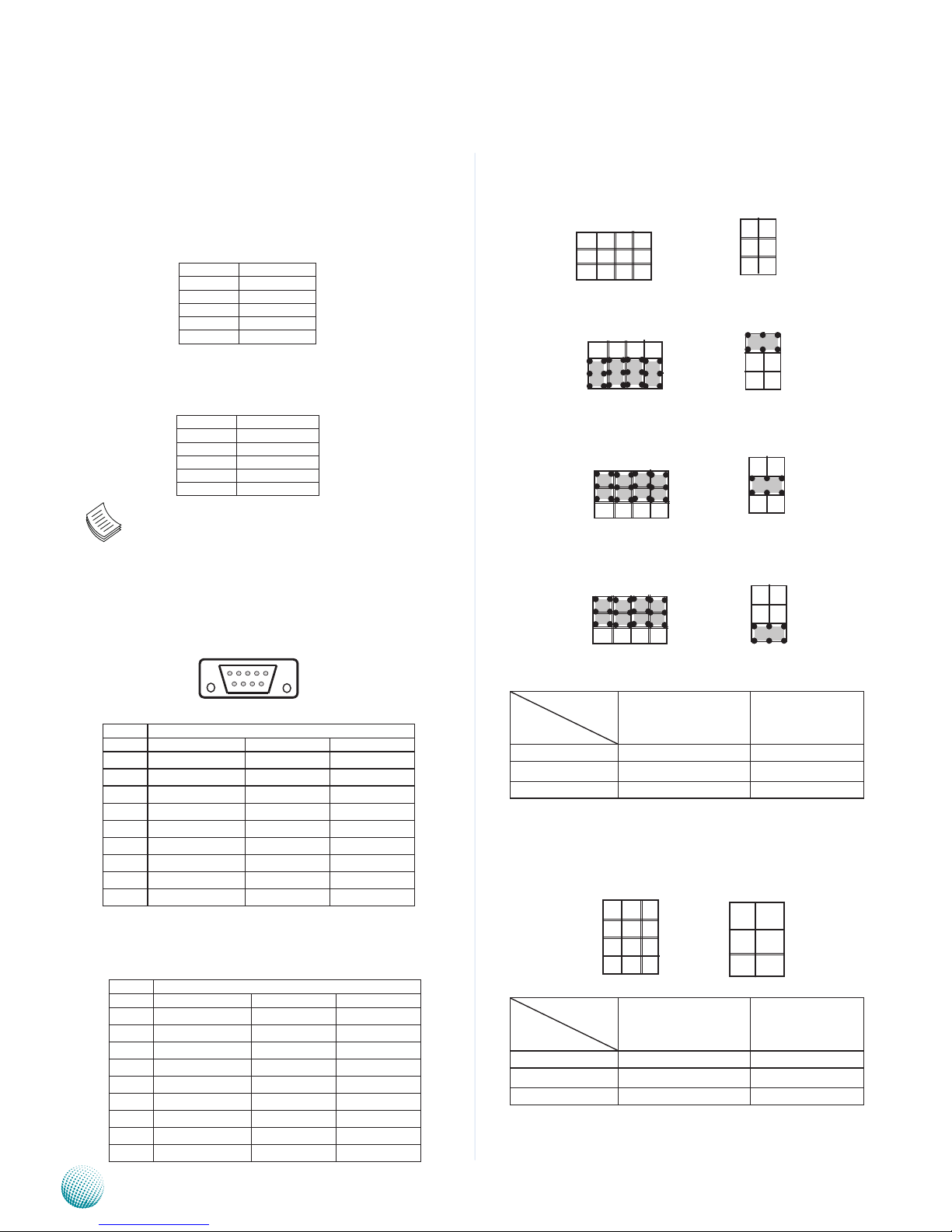
SCT1, SCT2: Select COM1 Protocol Setting
RS-232
RS-422
RS-485
Switch
Protocol
SCT1 SCT2
RS-232 (default) 1-5, 2-6, 3-7, 4-8 1-2
RS-422 5-9, 6-10, 7-11, 8-12 3-4
RS-485 5-9, 6-10, 7-11, 8-12 5-6
SCT3, SCT4: Select COM2 Protocol Setting
Switch
Protocol
SCT3 SCT4
RS-232 (default) 1-5, 2-6, 3-7, 4-8 1-2
RS-422 5-9, 6-10, 7-11, 8-12 3-4
RS-485 5-9, 6-10, 7-11, 8-12 5-6
Jumper Settings
Microphone-in Audio Jack (CN1)
Line-out Audio Jack (CN2)
Note: The driver for the VGA and Audio ports
should be installed with the following order:
Chipset INF->Graphic->Audio
COM1 RS-232 Serial Port(COM1): It is a RS-232/422/485
port through the D-SUB9 connector.
RS-232/422/485 Serial Port(COM2): It is a RS-232/422/485
port through the D-SUB9 connector.
6789
12345
Pin No. Function
1 CO_GND
2 MIC_INL
3 CO_GND
4 INSULATOR
5 MIC_INR
LEK-IOA2 Board
Pin No. Pin Name
RS-232 RS-422 RS-485
1 DCD TXD- DATA2 RXD TXD+ DATA+
3 TXD RXD+
4 DTR RXD5 GND
6 DSR
7 RTS
8 CTS
9 RI
Pin No. Function
1 CO_GND
2 LINOUT-L
3 CO_GND
4 INSULATOR
5 LINOUT- R
Pin No. Pin Name
RS-232 RS-422 RS-485
1 DCD TXD- DATA2 RXD TXD+ DATA+
3 TXD RXD+
4 DTR RXD5 GND
6 DSR
7 RTS
8 CTS
9 RI
SCT2
1
3
5
2
4
6
SCT1
9
5
1
12
8
4
9
5
1
12
8
4
1
3
5
2
4
6
1
3
5
2
4
6
1
3
5
2
4
6
9
5
1
12
8
4
9
5
1
12
8
4
SCT3
1
2
3
4
9
10
11
12
SCT4
1
3
5
2
4
6
Page 17
17
Board Layout
Chapter 3
Embedded and Industrial Computing
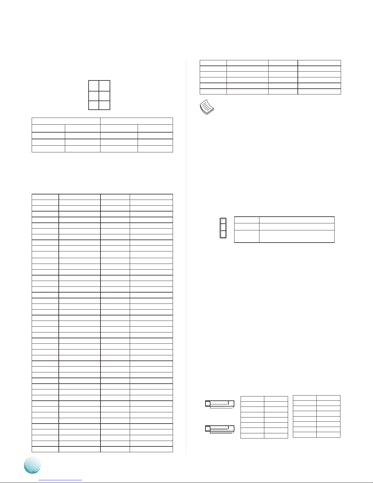
JP1, JP2: Select COM1 and COM2 Pin No9 (Ring Indicator)
function respectively
JP1 JP2
Pin Signal Pin Signal
1-2 VCC5 1-2 VCC5
3-4 VCC12 3-4 VCC12
5-6 SPI_RI 5-6 SPI_RI
MIO1 on the expansion card: Connector for connecting
the COM port and audio expansion board to the LEC-2280
main board.
PIN Pin Name PIN Pin Name
1 GND 51 HDA_BCLK
2 N/A 52 HDA_SYNC
3 N/A 53 HDA_RST
4 GND 54 HDA_SDIN0
5 N/A 55 HDA_SDO
6 N/A 56 SPK
7 GND 57 GND
8 VCC5 58 VCC3
9 VCC5 59 VCC3
10 N/A 60 N/A
11 GND 61 GND
12 N/A 62 N/A
13 N/A 63 N/A
14 N/A 64 N/A
15 N/A 65 N/A
16 N/A 66 N/A
17 N/A 67 N/A
18 GND 68 GND
19 N/A 69 N/A
20 N/A 70 N/A
21 GND 71 N/A
22 +12V 72 N/A
23 N/A 73 N/A
24 VCC5 74 N/A
25 VCC5 75 GND
26 VCC5 76 N/A
27 VCC5 77 N/A
28 GND 78 GND
29 N/A 79 N/A
30 N/A 80 N/A
31 N/A 81 N/A
32 N/A 82 N/A
33 GND 83 GND
34 N/A 84 COM1_DCD#
35 N/A 85 COM1_RI#
36 N/A 86 COM1_CTS#
37 N/A 87 COM1_DTR#
38 N/A 88 COM1_RTS#
39 N/A 89 COM1_DSR#
40 N/A 90 COM1_SOUT
41 N/A 91 COM1_SIN
42 GND 92 GND
43 N/A 93 COM2_DCD#
44 N/A 94 COM2_RI#
45 N/A 95 COM2_CTS#
46 N/A 96 COM2_DTR#
47 N/A 97 COM2_RTS#
48 N/A 98 COM2_DSR#
49 N/A 99 COM2_SOUT
50 N/A 100 COM2_SIN
Note: Daughter boards such as COM ports and
low-profile PCIe extension boards can only be
inserted to the mainboards with the same version.
Failure to do so may damage the system. The
board version is shown on top of the boards.
Clear CMOS jumper (CMOS1/CMOS2): It is for clearing
the CMOS data. CMOS 1clears CMOS data with real-time
clock (RTC) whereas CMOS2 clears CMOS data only.
To erase the CMOS data:
Turn off the computer and unplug the power cord.
Move the jumper cap from pins 1-2(default) to pins 1.
2-3. Keep the cap on pins 2-3 for about 5-10 seconds,
then move the cap back to pins 1-2.
Plug the power cord and turn on the computer.2.
Enter BIOS setup to re-enter data.3.
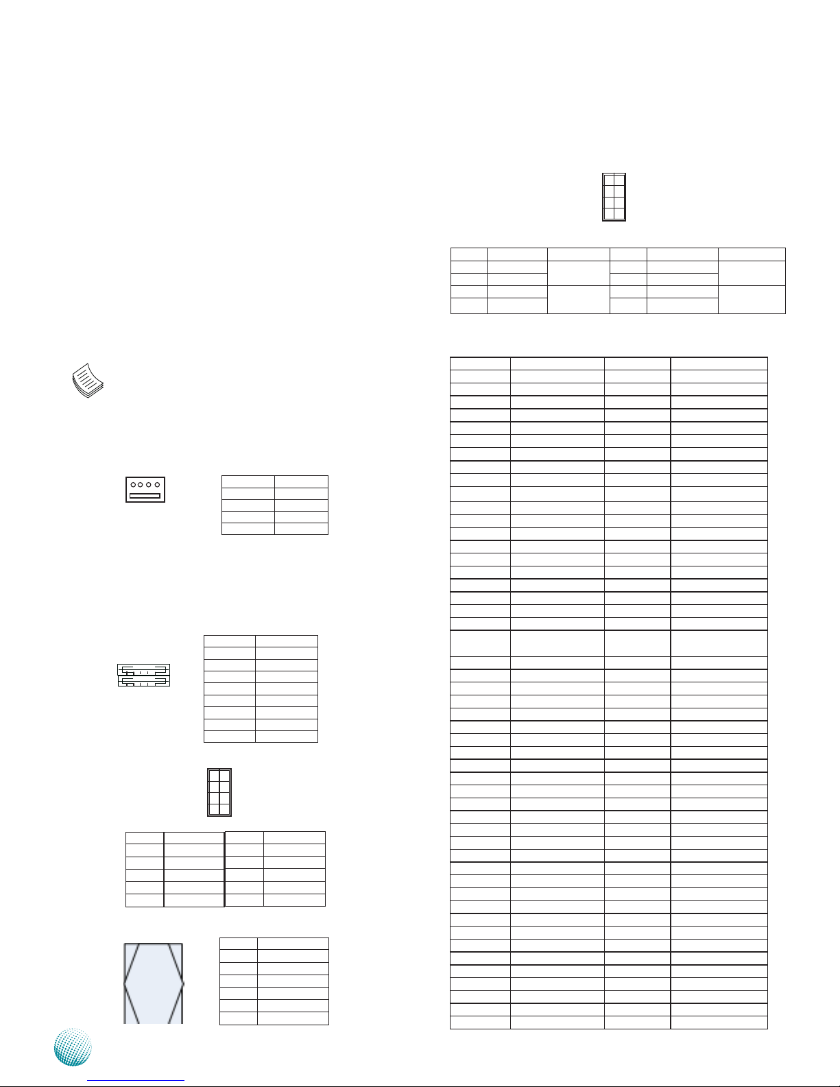
Serial-ATA Connector (SATA1/SATA2): It is for connecting
a 2.5’’ hard disk to be served as your system’s storage. It
can support SATA II which features Data transfer rates up
to 6.0 Gb/s (600 MB/s). SATA 2 connector also supports
SATA-DOM (the power line of SATA-DOM can be disabled
with a jumper on, see SATA_PW2).
Pin No. Pin Name
1-2 Normal (Default)
2-3 Clear CMOS and RTC (CMOS1)
Clear CMOS only (CMOS2)
1
2
3
1
3
5
2
4
6
Pin No. Function
1 GND
2 TX0_P
3 TX0_N
4 GND
5 RX0_N
6 RX0_P
7 GND
1 2 3 4 5 6 7
7 6 5 4 3 2 1
SATA1
SATA2
Pin No. Function
1 GND
2 TX1_P
3 TX1_N
4 GND
5 RX1_N
6 RX1_P
7 VCC5
LEB-2280 Board
Page 18
18
Board Layout
Chapter 3
Embedded and Industrial Computing
Front Panel Function Pin Header (FRONT1): It provides
LED signal and button function on the front panel.
Mini PCI Express Connector (MIO1) on the mainboard:
COM and Audio Expansion Card Connector
PIN Pin Name PIN Pin Name
1 GND 51 HDA_BCLK
2 SATATXN2 52 HDA_SYNC
3 SATATXP2 53 HDA_RST
4 GND 54 HDA_SDIN0
5 SATARXN2 55 HDA_SDO
6 SATARXP2 56 SPK
7 GND 57 VCC3_SB
8 VCC3P3_PS 58 VCC3_SB
9 VCC3P3_PS 59 VCC3_SB
10 VCC3P3_PS 60 VCC3_SB
11 GND 61 VCC3_SB
12 PCIE_RXN5 62 PCIE_RXN6
13 PCIE_RXP5 63 PCIE_RXP6
14 PCIE_TXN5 64 PCIE_TXN6
15 PCIE_TXP5 65 PCIE_TXP6
16 PCIE_CKN5 66 PCIE_CKN6
17 PCIE_CKP5 67 PCIE_CKP6
18 IGN_DI2 68 IGN_DI1
19 PLTRST 69 SMBCLK_
20 WAKE_N 70 SMBDATA
21 DCIN_VCC 71 REMOTE_POWER_
ON
22 VCC12_PS 72 3G_POWER_ON
23 VCC5_SB 73 USB_N12
24 VCC5_SB 74 USB_P12
25 VCC5 75 GND
26 VCC5 76 USB_N13
27 VCC5 77 USB_P13
28 GND 78 GND
29 DGOUT_0 79 DGIN_0
30 DGOUT_1 80 DGIN_1
31 DGOUT_2 81 DGIN_2
32 DGOUT_3 82 DGIN_3
33 GND 83 GND
34 COM3_DCD# 84 COM1_DCD#
35 COM3_RI# 85 COM1_RI#
36 COM3_CTS# 86 COM1_CTS#
37 COM3_DTR# 87 COM1_DTR#
38 COM3_RTS# 88 COM1_RTS#
39 COM3_DSR# 89 COM1_DSR#
40 COM3_SOUT 90 COM1_SOUT
41 COM3_SIN 91 COM1_SIN
42 GND 92 GND
43 COM4_DCD# 93 COM2_DCD#
44 COM4_RI# 94 COM2_RI#
45 COM4_CTS# 95 COM2_CTS#
46 COM4_DTR# 96 COM2_DTR#
47 COM4_RTS# 97 COM2_RTS#
48 COM4_DSR# 98 COM2_DSR#
49 COM4_SOUT 99 COM2_SOUT
50 COM4_SIN 100 COM2_SIN
The controller contains two modes of operation—a
legacy mode using I/O space, and an AHCI mode using
memory space. Software that uses legacy mode will not
have AHCI capabilities.
The AHCI ( Advanced Host Controller Interface) is a
programming interface which defines transactions
between the SATA controller and software and enables
advanced performance and usability with SATA. Platforms
supporting AHCI may take advantage of performance
features such as no master/slave designation for SATA
devices—each device is treated as a master—and
hardware assisted native command queuing. AHCI also
provides usability enhancements such as Hot-Plug.
Use the BIOS menu to configure your hard disk
to be AHCI compatible.
4-pin Serial-ATA Power Connector (PWR1): It is for
connecting the SATA power cord.
Dual USB 2.0 Port Connector #0 and #1 (USB1)
Dual USB 2.0 Port Connector #2 and #3 (USB2)
Dual USB 2.0 Port Connector #4 and #5 (USB3)
USB 2.0 Pin Header (USB4):
SIM Card Socket (SIM1):
10
8
6
4
2
9
7
5
3
1
Pin No. Description
C1 UIM_PWR
C2 UIM_RST
C3 UIM_CLK
C5 GND
C6 UIM_VPP
C7 UIM_DAT
C5 C7
C1 C3
1 2 3 4
5 6 7 8
Pin No. Pin Name
1 VCCUSB
2 USB0N
3 USB0P
4 GND
5 VCCUSB1
6 USB1N
7 USB1P
8 GND
Pin No. Pin Name
1 VCCUSB10
3 N/A
5 USB10N
7 USB10P
9 GND
Pin No. Pin Name
2 GND
4 USB11P
6 USB11N
8 N/A
10 VCCUSB11
1
3
5
7
9
2
4
6
8
10
Pin No. Function
1 +12V
2 GND
3 GND
4 +5V
4 3 2 1
Pin No. Pin Name Function Pin No. Pin Name Function
1 HD_LED+ HDD LED 2 PWR_LED+ Power LED
3 HD_LED- 4 PWR_LED5 Reset System Reset
Button
6 POWER_BTN Power On/Off
Push Button
7 GND 8 GND
Page 19
19
Board Layout
Chapter 3
Embedded and Industrial Computing
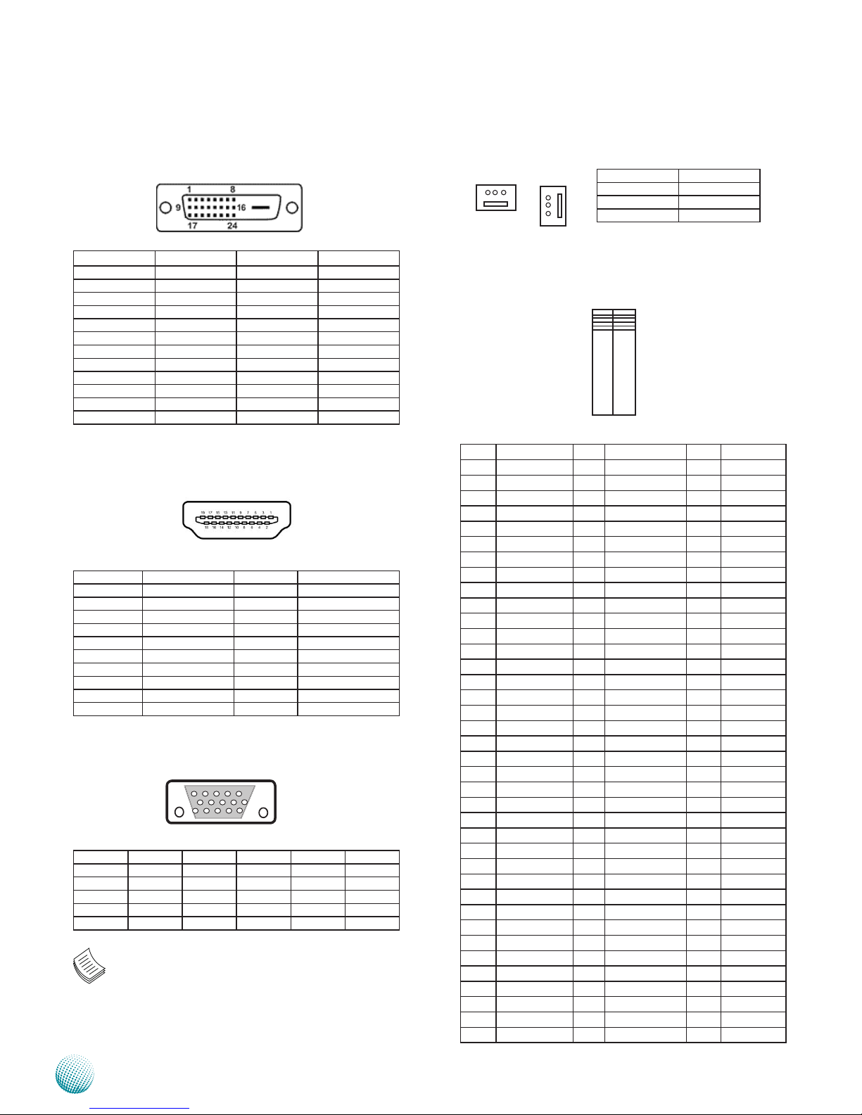
DVI-D Connector (DVID1): A single link DVI-D Connector
Pin No. Description Pin No. Description
1 TXD_2- 2 TXD_2+
3 GND 4 N/A
5 N/A 6 DDC_CLK
7 DDC_DATA 8 N/A
9 TXD_1- 10 TXD_1+
11 GND 12 N/A
13 N/A 14 VCC5
15 GND 16 HPD
17 TXD_0- 18 TXD_0+
19 GND 20 N/A
21 N/A 22 GND
23 TXD_CLK_P 24 TXD_CLK_N
HDMI Connector (HDMI1): An HDMI Connector
Pin No. Description Pin No. Description
1 HDMI_DATP2_P 2 GND
3 HDMI_DATP2_N 4 HDMI_DATP1_P
5 GND 6 HDMI_DATP1_N
7 HDMI_DATP0_P 8 GND
9 HDMI_DATP0_N 10 HDMI_CLK_P
11 GND 12 HDMI_CLK_N
13 N/A 14 N/A
15 HDMI_DDC_CLK 16 HDMI_DDC_DAT
17 GND 18 PHDMI
19 HDMI_HPD
VGA (VGA1)
Pin Signal Pin Signal Pin Signal
1 RED 6 CRT DET 11 N/A
2 GREEN 7 GND 12 DDC DAT
3 BLUE 8 GND 13 HSYNC
4 N/A 9 VCC5 14 VSYNC
5 GND 10 GND 15 DDC CLK
Note: The driver for the VGA and Audio ports
should be installed with the following order:
Chipset INF->Graphic->Audio
System FAN Connector (FAN1/FAN2)
Pin No. Description
1 GND
2 VCC5
3 FAN TAC
PCI/PCIE Expansion connector for PCI or PCIe low
prole card (PCIEIO1, on the backside)
PIN SIGNAL PIN SIGNAL PIN SIGNAL
1 VCC3P3_SB 53 PCIE_CKP1 105 PEG_RXP9
2 VCC5_SB 54 PCIE_TXP1 106 PEG_TXP9
3 VCC3P3_SB 55 PCIE_CKN1 107 GND
4 VCC5_SB 56 PCIE_TXN1 108 GND
5 N/A 57 GND 109 PEG_RXN8
6 N/A 58 GND 110 PEG_TXN8
7 VCC3P3_ 59 PEGACLKN 111 PEG_RXP8
8 V1P5 60 PEGBCLKN 112 PEG_TXP8
9 VCC3P3_ 61 PEGACLKP 113 GND
10 N/A 62 PEGBCLKP 114 GND
11 VCC3P3_ 63 GND 115 PEG_RXN7
12 VCC5 64 GND 116 PEG_TXN7
13 VCC3P3_ 65 GND 117 PEG_RXP7
14 VCC5 66 GND 118 PEG_TXP7
15 VCC3P3_ 67 PEG_RXN15 119 GND
16 VCC5 68 PEG_TXN15 120 GND
17 VCC3P3_ 69 PEG_RXP15 121 PEG_RXN6
18 VCC5 70 PEG_TXP15 122 PEG_TXN6
19 N/A 71 GND 123 PEG_RXP6
20 VCC5 72 GND 124 PEG_TXP6
21 GND 73 PEG_RXN14 125 GND
22 VCC5 74 PEG_TXN14 126 GND
23 N/A 75 PEG_RXP14 127 PEG_RXN5
24 N/A 76 PEG_TXP14 128 PEG_TXN5
25 +12V 77 GND 129 PEG_RXP5
26 GND 78 GND 130 PEG_TXP5
27 +12V 79 PEG_RXN13 131 GND
28 GND 80 PEG_TXN13 132 GND
29 +12V 81 PEG_RXP13 133 PEG_RXN4
30 CLKRQ1 82 PEG_TXP13 134 PEG_TXN4
31 +12V 83 GND 135 PEG_RXP4
32 CLKRQ2 84 GND 136 PEG_TXP4
33 N/A 85 PEG_RXN12 137 GND
34 GND 86 PEG_TXN12 138 GND
35 PLTRST 87 PEG_RXP12 139 PEG_RXN3
36 SMBCLK 88 PEG_TXP12 140 PEG_TXN3
37 WAKE_N 89 GND 141 PEG_RXP3
38 SMBDATA 90 GND 142 PEG_TXP3
1
159
2
160
3 2 1
FAN1
3
2
1
FAN2
15 14 13 12 11
5 4 3 2 1
Page 20
20
Board Layout
Chapter 3
Embedded and Industrial Computing
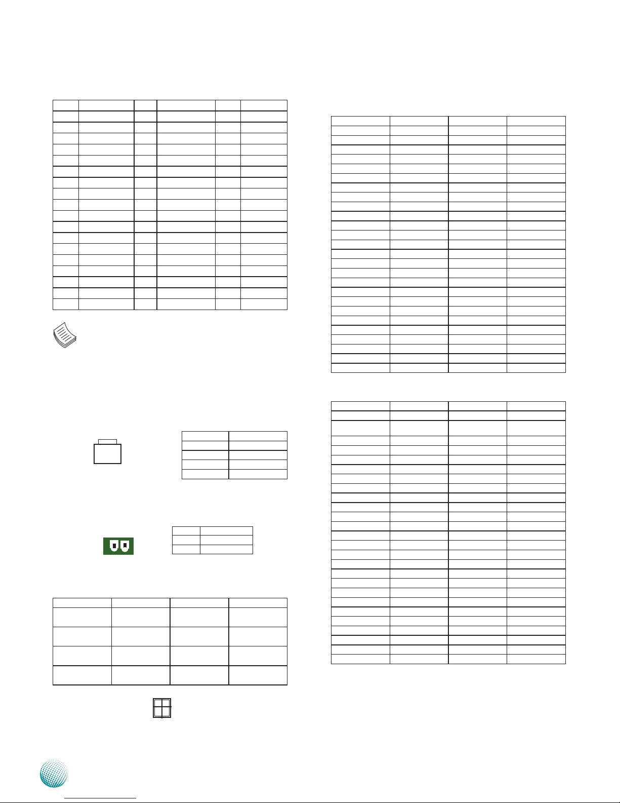
MPCIE1: Mini-PCIe Connector with SIM Card Reader
Pin Signal Pin Signal
1 WAKE# 2 VCC3.3
3 N/A 4 GND
5 N/A 6 VCC1.5
7 CLKREQ# 8 USIM_PWR
9 GND 10 UIM_DATA
11 PCIE_CLK_N3 12 UIM_CLK
13 PCIE_CLK _P3 14 UIM_RESET
15 GND 16 UIM_VPP
17 RSV 18 GND
19 RSV 20 N/A
21 GND 22 PLTRST
23 PCIE_RX_N3 24 VCC3.3
25 PCIE_RX_P3 26 GND
27 GND 28 VCC1.5
29 GND 30 SMBCLK
31 PCIE_TX_N3 32 SMBDATA
33 PCIE_TX_P3 34 GND
35 GND 36 USB_N8
37 GND 38 USB_P8
39 VCC3.3 40 GND
41 VCC3.3 42 N/A
43 GND 44 N/A
45 RSV 46 N/A
47 RSV 48 VCC1.5
49 RSV 50 GND
51 RSV 52 VCC3.3
MPCIE2: Mini-PCIe Connector
Pin Signal Pin Signal
1 WAKE# 2 VCC3.3
3 N/A 4 GND
5 N/A 6 VCC1.5
7 CLKREQ# 8 N/A
9 GND 10 N/A
11 PCIE_CLK _N4 12 N/A
13 PCIE_CLK _P4 14 N/A
15 GND 16 N/A
17 RSV 18 GND
19 RSV 20 N/A
21 GND 22 PLTRST
23 PCIE_RX_N4 24 VCC3.3
25 PCIE_RX_P4 26 GND
27 GND 28 VCC1.5
29 GND 30 SMBCLK
31 PCIE_TX_N4 32 SMBDATA
33 PCIE_TX_P4 34 GND
35 GND 36 USB_N9
37 GND 38 USB_P9
39 VCC3.3 40 GND
41 VCC3.3 42 N/A
43 GND 44 N/A
45 RSV 46 N/A
47 RSV 48 VCC1.5
49 RSV 50 GND
51 RSV 52 VCC3.3
PIN SIGNAL PIN SIGNAL PIN SIGNAL
39 GND 91 PEG_RXN11 143 GND
40 GND 92 PEG_TXN11 144 GND
41 PCIE_RXN2 93 PEG_RXP11 145 PEG_RXN2
42 PCIE_CKN2 94 PEG_TXP11 146 PEG_TXN2
43 PCIE_RXP2 95 GND 147 PEG_RXP2
44 PCIE_CKP2 96 GND 148 PEG_TXP2
45 GND 97 PEG_RXN10 149 GND
46 GND 98 PEG_TXN10 150 GND
47 PCIE_RXP1 99 PEG_RXP10 151 PEG_RXN1
48 PCIE_TXN2 100 PEG_TXP10 152 PEG_TXN1
49 PCIE_RXN1 101 GND 153 PEG_RXP1
50 PCIE_TXP2 102 GND 154 PEG_TXP1
51 GND 103 PEG_RXN9 155 GND
52 GND 104 PEG_TXN9 156 GND
157 PEG_RXN0
158 PEG_TXN0
159 PEG_RXP0
160 PEG_TXP0
Note: Daughter boards such as COM ports and
low-profile PCIe extension boards can only be
inserted to the mainboards with the same version.
Failure to do so may damage the system. The
board version is shown on top of the boards.
Reset Button (RST1)
Pin NO. Description
1 RST_BTN
2 GND
3 GND
4 N/A
DC_IN CONNECTOR (CN4): A Phoenix connector for
external power supply.
J1(PEG 16X lane function): PCI/PCIe (PCIEIO1) expansion
connector signal selection
Pin Lane Function1 Function2
(1) (3)
H H
x16 DISABLE DISABLE
(1) (3-4)
H L
x8, x8 ENABLE DISABLE
(1-2) (3)
L H
Reserved DISABLE ENABLE
(1-2) (3-4)
L L
x8, x4, x4 ENABLE ENABLE
Pin No. Pin Name
1 GND
2 DC_VIN
1
3
2
4
1 2
1
3
2
4
Page 21
21
Board Layout
Chapter 3
Embedded and Industrial Computing
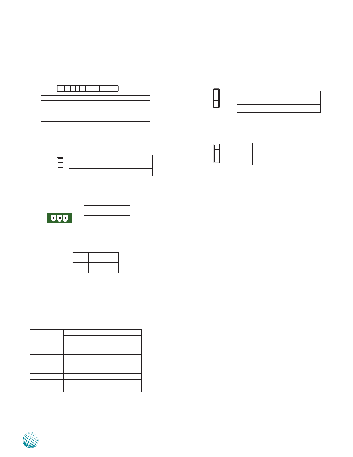
Ignition Connector on board (ignition1): Power
ignition connector.
SATA_PW2: A switch for supply of SATA Connector II’s
power.
CN3 (optional): An optional power connector with
power -ignition Control
DCJK1 (Optional): An optional DC Jack type of Power
Connector
LAN1/LAN2 Ports (LAN1/LAN2): The LAN ports are
provided by Intel 82574L Ethernet controller whose
interface complies with PCI-e 1.1 (2.5 Ghz). It has advanced
management features including IPMI pass-through via
SMBus or NC-SI, WOL, PXE remote boot, ISCSI boot and
VLAN filtering.
Pin No. Description
Fast Ethernet Gigabit Ethernet
1 TX+ BI_DA+
2 TX- BI_DA3 RX+ BI_DB+
4 -- BI_DC+
5 -- BI_DC6 RX- BI_DB7 -- BI_DD+
8 -- BI_DD-
Pin No. Pin Name
1 Ignition
2 GND
3 DC_VIN
Pin No. Pin Name
1-2 SATAII Connector without power
2-3 SATA II Connector with 5V power
Pin No. Pin Name Pin No. Pin Name
1 DCIN_VCC 6 DC2DC_PWROK
2 DC_VIN 7 COM5_SIN
3 GND 8 SOUT
4 SYS_PWROK 9 PWR_BTN_IGN
5 DC2DC_EN 10 IGNITION
1 2 3 4 10
1
2
3
Pin No. Pin Name
1 DC_VIN
2 GND
3 GND
1 2 3
Enable or Disable Daughter Board LEK-IOA3 (COMSLT1):
This jumper is for enabling or disabling daughter board
LEK-IOA3.
Enable or Disable Daughter Board LEK-IG1 (COMSLT2):
This jumper is for enabling or disabling daughter board
LEK-IG1.
Pin No. Pin Name
1-2 Disable
2-3 Enable
Pin No. Pin Name
1-2 Disable
2-3 Enable
1
2
3
1
2
3
Page 22
22
Hardware Setup
Chapter 4
Embedded and Industrial Computing
Chapter 4:
Hardware Setup
Preparing the Hardware Installation
To access some components and perform certain service
procedures, you must perform the following procedures
first.
WARNING: To reduce the risk of personal injury,
electric shock, or damage to the equipment,
remove the power cord to remove power from
the server. The power switch button does not
completely shut off system power. Portions of the
power supply and some internal circuitry remain
active until power is removed.
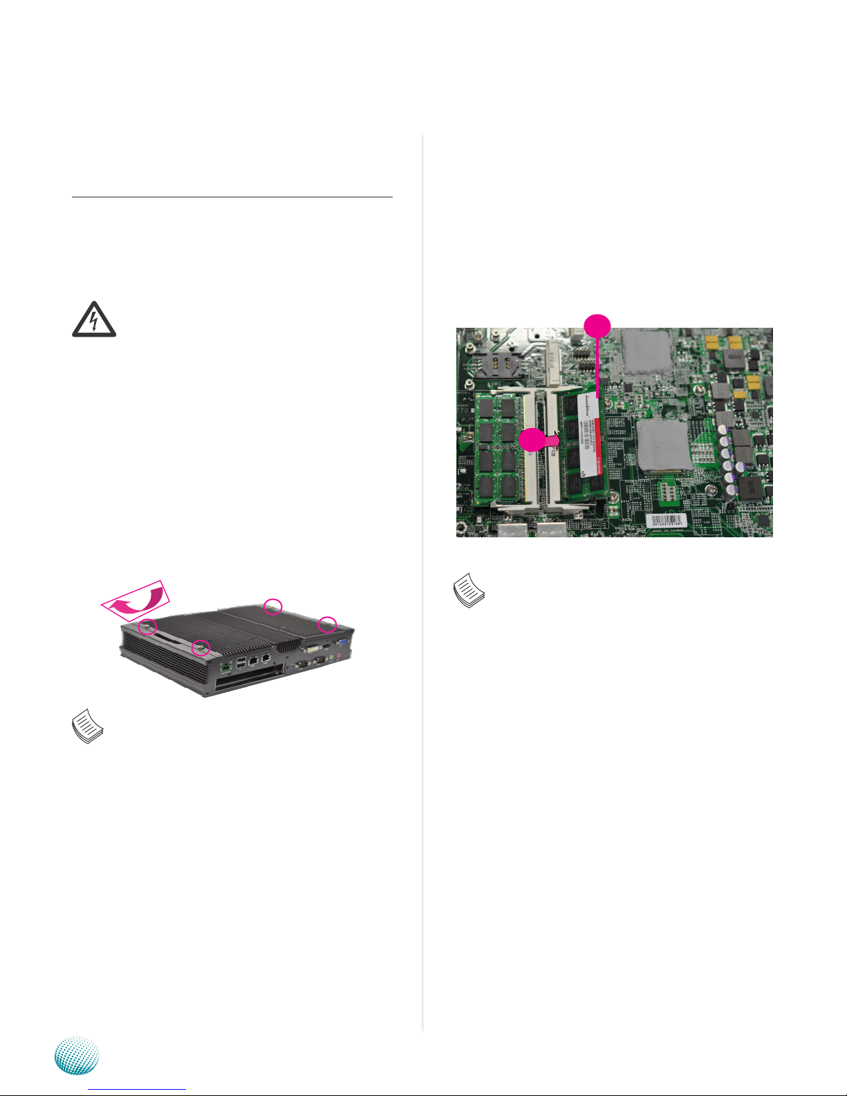
Unpower the LEC-2280 and remove the power cord.1.
Unscrew the 4 threaded screws from the top cover.2.
Open the cover.3.
Note:
If the CPU thermal pad mounting breaks apart,
use your hands to reattach the falling parts and
stick them together.
Installing the System Memory
The motherboard supports DDR3 memory to meet the
higher bandwidth requirements of the latest operating
system and Internet applications. It comes with two
Double Data Rate Three (DDR3) Small Outline Dual Inline
Memory Module (SO-DIMM) socket.
Align the memory module’s cutout with the SO-DIMM 1.
socket’s notch.
Install the SO-DIMM.2.
Note:
The system can support memory of DDR3 SODIMM up to 16 GB in maximum with 2 SO-DIMM
sockets.
1
2
Page 23
23
Hardware Setup
Chapter 4
Embedded and Industrial Computing
Note: To remove the SIM card, slide the card
reader outward to unlock it.
PCI/PCIe Riser Card Installation
The system can accommodate one PCIe expansion (or two
PCI expansion on model P2) module. In order the install
the PCIe expansion module, a low-profile riser card has
to be installed first. Follow these steps to install the riser
card:
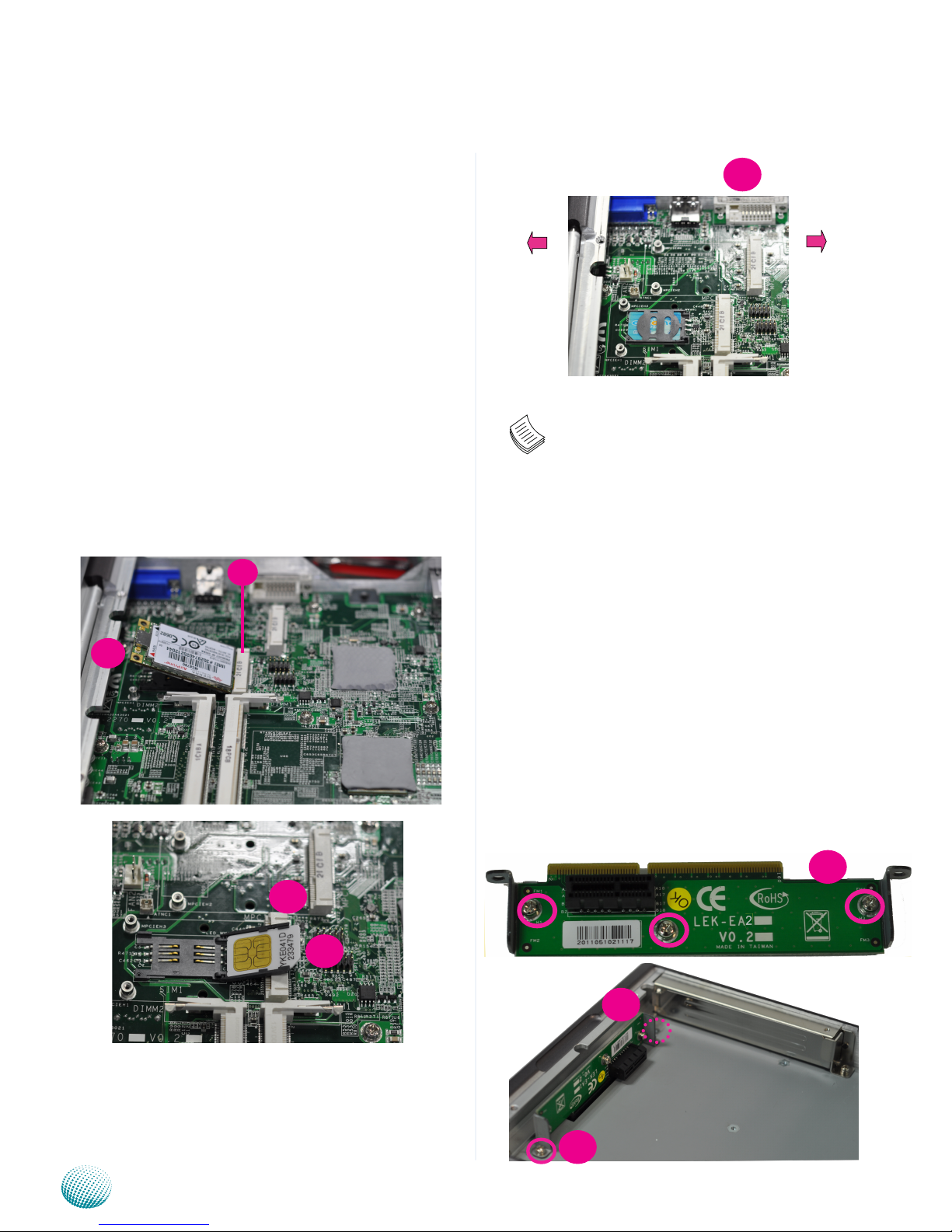
Fix the riser card on the bracket with 3 screws.1.
Install the riser card to the system by connecting the 2.
connectors with the system’s PCIEIO1 connector.
Fix the riser card on the board.3.
Connect the PCIe expansion card to the riser.4.
Fix the card holder back to the system.5.
On 2280E with one PCIe slot
Wireless Module Installation
Align the wireless module’s cutout with the Mini-PCIe 1.
slot notch.
Insert the wireless module into the connector 2.
diagonally.
Hold down the other end of the wireless module and 3.
tighten it with the screws.
3G SIM Card Installation
Unlink the SIM card reader first by sliding it outward.1.
Flip the SIM card reader diagonally.2.
Align the cut corner of the SIM card pointing toward 3.
SIM card reader. Make sure the ICs will be in contact
with the SIM card reader.
Insert the 4. SIM card into the reader and close the tray.
You should feel a click when the SIM card is locked
securely in the SIM card reader.
Lock
Unlock
1
2
3
2
3
4
2
3
Page 24
24
Hardware Setup
Chapter 4
Embedded and Industrial Computing
Installing the Hard Disk
The system can accommodate one Serial-ATA disk. Follow
these steps to install a hard disk into the system:
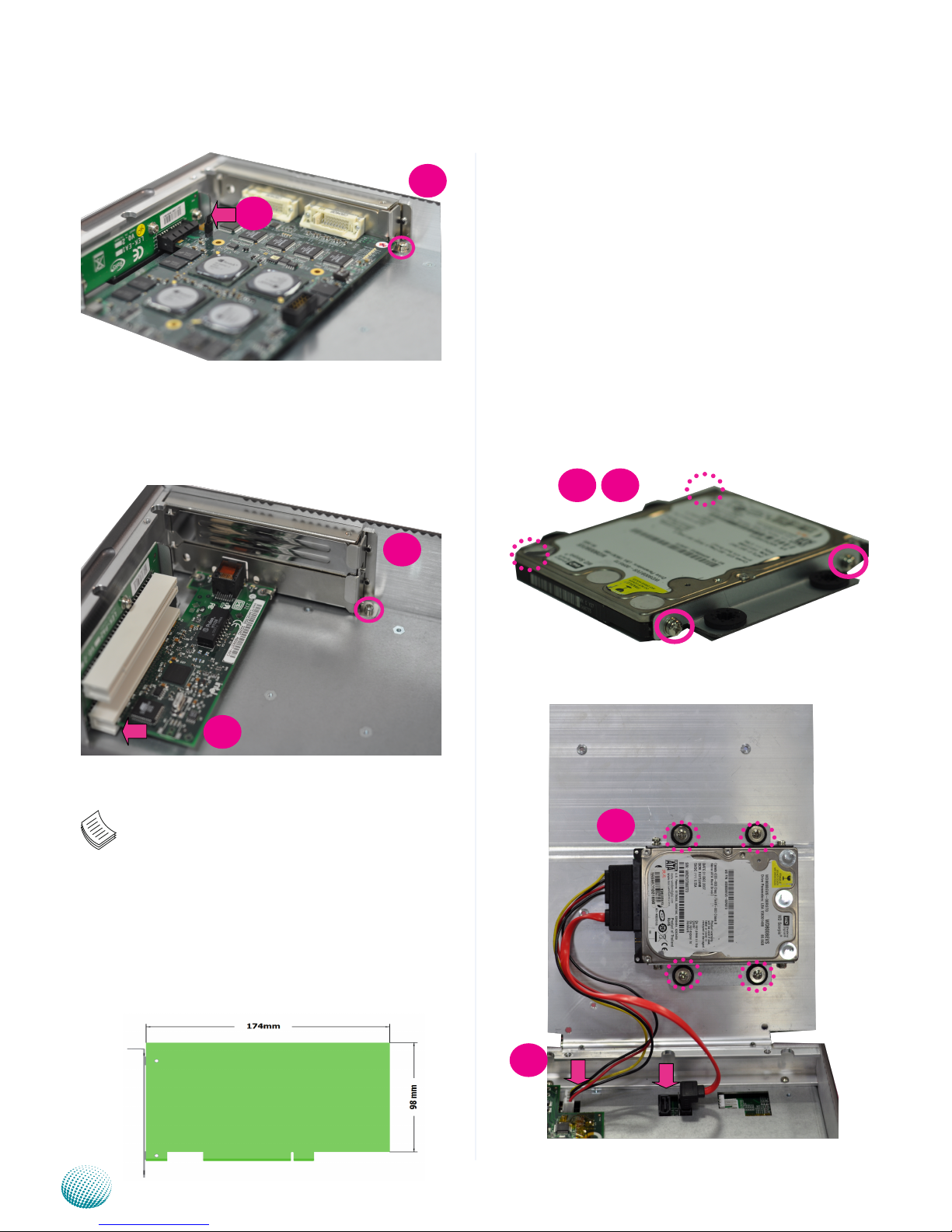
Take out the hard disk tray and fix the hard disk on 1.
the tray with 4 mounting screws as illustrated in the
following picture.
Plug the Serial-ATA cable to the hard disk.2.
Place the hard disk back to the system’s chassis and fix 3.
it with the mounting screws.
Connect the Serial-ATA power and data disk cables to 4.
the Serial-ATA power and disk connectors on the main
board respectively.
On 2280P2 with 2 PCI slot
Note: Using a PCIe or PCI riser card, users have
choice of either PCI Express x1 or PCI expansions.
1 PCIe is supported on model LEC-2280E1.
2 PCI are supported on model LEC-2280P22.
Both PCI or PCIe support the Max. Dimension 3.
as the following illustrated and the Max.
Power consumption reserved for expansion is
25W in total.
Daughter boards such as COM ports and 4.
low-profile PCIe extension boards can only
be inserted to the mainboards with the same
version. The board version is shown on top of
the boards.
5.
1
2
3
4
4
5
4
5
Page 25
25
Hardware Setup
Chapter 4
Embedded and Industrial Computing
Wall Mounting
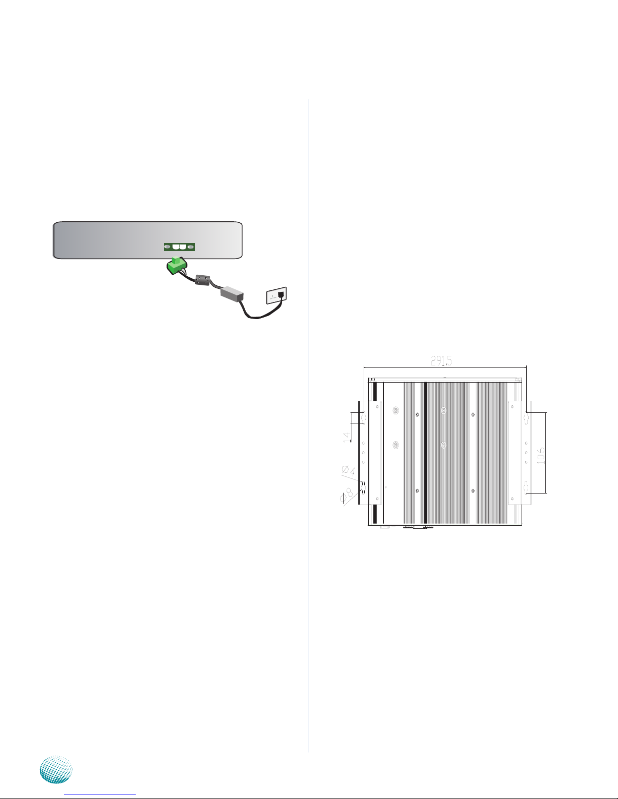
The product ships with wall mounting kit. To mount your
product on the wall, follow the instructions below:
First make a hole for the anchor in the surface on the 1.
wall. Use the following diagram as a guideline for
placing the anchors.
Then press the anchor into the hole until it is flush with 2.
the surface. You may need a hammer to tap the wall
anchor.
Use a screwdriver to screw the threaded screw into the 3.
plastic anchor.
Attach the wall mounting bracket to the back of the 4.
device, securing it in place with four of the flat-head
screws provided.
Hang the device on the wall.5.
Connecting Power
Connect the LEC-2280 to a +9~+30V DC-in power source.
The DC power-in connector comes with a 2-pin terminal
block for its Phoenix contact. This power socket can only
accept the power supply with the right pin contact so be
cautious when inserting power to the system.
Unit: mm
DC IN
– +
Page 26
26
Programming Watchdog Timer
Embedded and Industrial Computing
Appendix A
Appendix A:
Programming Watchdog
Timer
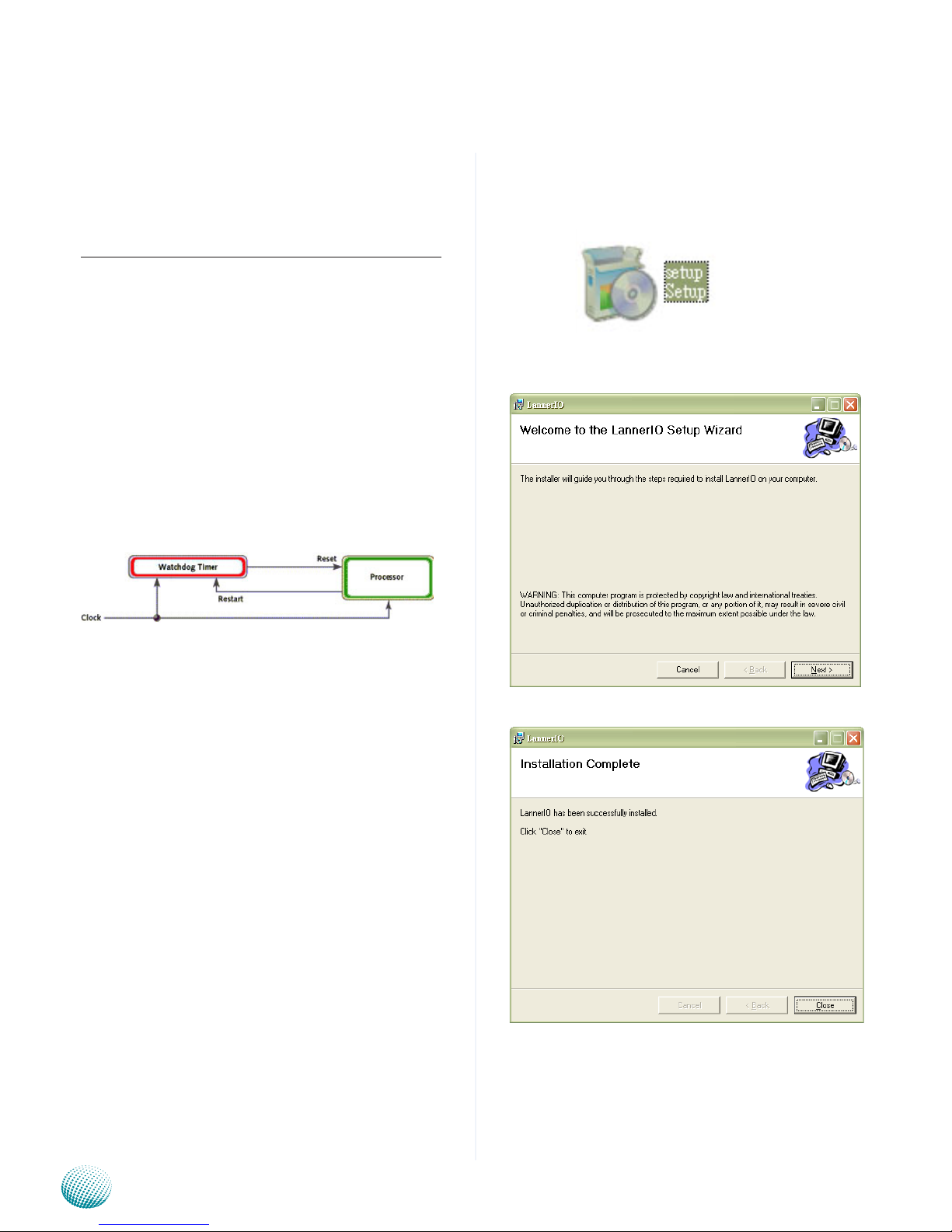
A watchdog timer is a piece of hardware that can be
used to automatically detect system anomalies and reset
the processor in case there are any problems. Generally
speaking, a watchdog timer is based on a counter that
counts down from an initial value to zero. The software
selects the counter’s initial value and periodically restarts
it. Should the counter reach zero before the software
restarts it, the software is presumed to be malfunctioning
and the processor’s reset signal is asserted. Thus, the
processor will be restarted as if a human operator had
cycled the power.
For sample watchdog code, see Watch dog and DIO folder
in the Driver and Manual CD
Driver Installation
Before you could access or control the operation of the
watchdog and Digital I/O functions, install the the L_IO
driver which is the library and driver needed for Lanner
General Purpose Input/Output interface or functions.
To install the L_IO driver:
Restart the computer, and then log on with 1.
Administrator privilege.
Insert the Drivers and User’s Manual CD to the USB-2.
optical drive.
Browse the contents of the support CD to locate the 3.
file LannerIO v101.rar under the \WD_DIO\ folder and
unzip the file.
Click the Setup program in the unzipped folder.4.
Click the Setup program.1.
The welcome screen appears. Click Next to proceed.2.
The installation process proceeds. Click Close when the 3.
process completes.
Page 27
27
Programming Watchdog Timer
Embedded and Industrial Computing
Appendix A
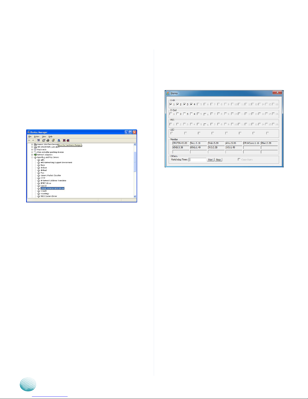
To verify the GPIO driver installation, do the following
steps:
Right-click on the My Computer icon, and then select 1.
Properties form the menu.
Click the Hardware tab, then click the Device Manager 2.
button.
Select 3. View from the menu and select show hidden
devices .
The Lanner common GPIO driver should be listed 4.
under the Non-Plug and Play Drivers. If not, click the
San for hardware changes button from the tool bar.
Sample Program
Via the Demo Program
Enter the number of seconds to start count down before
the system can be reset. Press start to start the counter
and stop to stop the counter.
Via the Command Line
Execute the executable file in the program folder, then
enter the values from 1~255. The system will reboot
automatically according to the time-out you set.
wd_tst --swt xxx (Set Watchdog Timer 1-255 seconds)
wd_tst[*] --start (Start Watchdog Timer)
wd_tst --stop (Stop Watchdog Timer)
Page 28

28
Programming Watchdog Timer
Embedded and Industrial Computing
Appendix A
Source Code
You can write your own program by modifying the source
code F81865_Test.cpp.. The index address is 2EH.
/////////////////////////////////////////////////////////////////////
////
// F81865_Test.cpp : F81865_test.exe utility for F81865.lib
APIs demonstration.
//
// History:
// 7/15/2011 Brand new F81865_test
program.
#include <winsock2.h>
#include “Windows.h”
#include “stdio.h”
#include “F81865.h”
#define PARAMETER_HELP “\n”\
“The F81865 GPIO utility of Lanner\n”\
“-------------------------------------\n”\
“Usage:\n”\
“ F81865_test DIO_IN port_
number\n”\
“ F81865_test DIO_OUT port_number
value\n”\
“ F81865_test PIO port_number
value\n”\
“ F81865_test RunLED port_number
value\n”\
“ F81865_test AlarmLED port_number
value\n”\
“ F81865_test GPS_LED port_number
value\n”\
“ F81865_test WirelessLED port_number
value\n”\
“ F81865_test WatchDog seconds\n”\
“ F81865_test CaseOpen\n”\
“ F81865_test CaseOpen_Clear\n”\
“ F81865_test Sleep
milliseconds\n”\
“\n”\
“Argement:\n”\
“ DIO_IN Read state from DIO
In.\n”\
“ DIO_OUT Set DIO Out state.\n”\
“ PIO Set PIO LED state.\n”\
“ RunLED Set RUN LED state.\n”\
“ AlarmLED Set Alarm LED state.\n”\
“ GPS_LED Set GPS LED state.\n”\
“ WirelessLED Set Wireless LED state.\n”\
“ Watchdog Set
Watchdog timer.\n”\
“ CaseOpen Check case opened state.\n”\
“ CaseOpen_Clear Clear case open state.\n”\
“ port_number The port number.\n”\
“ value 1 for on and 0 for off.\n”\
“ seconds The
watchdog count down seconds. 0 for disable.\n”\
“ milliseconds Milliseconds to
delay\n”
#define RETMSG(a,b) {printf (b) ; return a;}
#define CHECK_ARGC(a) {if (argc
!= a) throw PARAMETER_HELP ;}
// Translate Hex string to a long value
LONG Hex2Long (char *str)
{
LONG nLong ;
if (scanf (str, “%x”, &nLong) != 1)
throw “Error parsing parameter\n” ;
return nLong ;
}
Page 29

29
Programming Watchdog Timer
Embedded and Industrial Computing
Appendix A
// Make sure the argument is numeric
void CheckNumeric (char *szBuf )
{
int nLen = strlen (szBuf) ;
for (int i = 0 ; i < nLen ; i++)
if (!strchr (“01234567890ABCDEFabcdef”, szBuf[i]) )
throw “Wrong argument\n” ;
}
// Common GPIO output function definition
#define GPIO_OUT(a,b,c) \
int a (int argc, char *argv[]) \
{
\
CHECK_ARGC (4) ;
\
CheckNumeric (argv[2]) ; \
CheckNumeric (argv[3]) ; \
\
int nPort = atoi (argv[2]) ; \
int nValue = atoi (argv[3]) ; \
\
c (nPort, nValue) ;
\
\
printf (b “ #%d = %d\n”, nPort, nValue) ; \
\
return 0
; \
}
// Function generate by common function definition
GPIO_OUT (mDIO_
OUT , “DIO_OUT” , Write_DIO)
G P I O _ O U T
(mPIO , “DIO_OUT” , PIO)
G P I O _ O U T
(mRunLED , “RunLED” , RunLED)
G P I O _ O U T
(mAlarmLED , “AlarmLED” , AlarmLED)
GPIO_OUT (mGPS_
LED , “GPS_LED” , GPS_LED)
G P I O _ O U T
(mWirelessLED , “WirelessLED” , WirelessLED)
// Check case open
int mCaseOpen (int argc, char* argv[])
{
CHECK_ARGC (2) ;
BOOL bOpen = CaseOpen () ;
printf (“Case is %s\n”, bOpen ? “Open” : “Close”) ;
return bOpen ;
}
// Clear case open state
int mCaseOpen_Clear (int argc, char* argv[])
{
CHECK_ARGC (2) ;
CaseOpen_Clear () ;
BOOL bOpen = CaseOpen () ;
printf (“CaseOpen state %s”, bOpen ? “not cleared”
: “cleared”) ;
return bOpen ;
}
// Get DIO_IN state
int mDIO_IN (int argc, char* argv[])
{
CHECK_ARGC (3) ;
CheckNumeric (argv[2]) ;
int nPort = atoi (argv[2]) ;
Page 30

30
Programming Watchdog Timer
Embedded and Industrial Computing
Appendix A
BOOL ret = Read_DIO (nPort) ;
printf (“DIO_IN #%d = %d\n”, nPort, ret) ;
return ret ;
}
// Milli-second delay
int mSleep (int argc, char *argv[])
{
CHECK_ARGC (3) ;
CheckNumeric (argv[2]) ;
Sleep (atoi (argv[2]) ) ;
return 0 ;
}
// Watchdog
int mWatchDog (int argc, char *argv[])
{
if (argc != 3 && argc != 2)
RETMSG (-1, PARAMETER_HELP) ;
if (argc == 3)
{
CheckNumeric (argv[2]) ;
int nValue = atoi (argv[2]) ;
WatchDog_Enable (nValue) ;
}
int nLeft = WatchDog_GetLeft () ;
printf (“Watchdog timer left %d seconds\n”, nLeft)
;
return nLeft ;
}
// Argument - function mapping
typedef struct
{
char *szCmd ;
int (*function) (int argc, char *argv[]) ;
} CMD2FUN ;
CMD2FUN c2f[] =
{
{“DIO_IN” , mDIO_IN
},
{“DIO_OUT” , mDIO_OUT
},
{“PIO” , mPIO
},
{“RunLED” , mRunLED
},
{“AlarmLED” , mAlarmLED
},
{“GPS_LED” , mGPS_LED
},
{“WirelessLED” , mWirelessLED },
{“CaseOpen” , mCaseOpen },
{“CaseOpen_Clear”,mCaseOpen_Clear},
{“Watchdog” , mWatchDog
},
{“Sleep” , mSleep }
} ;
// Program start here
int main(int argc, char *argv[])
{
Page 31

31
Programming Watchdog Timer
Embedded and Industrial Computing
Appendix A
try
{
// The total argument allowed
int num = sizeof (c2f ) / sizeof (c2f[0]) ;
// Too few argument
if (argc < 2)
RETMSG (-1, PARAMETER_HELP)
;
// Find the match argument and execute
the mapping function
for (int i = 0 ; i < num ; i++)
if (stricmp (argv[1], c2f[i].szCmd)
== 0)
return c2f[i].function
(argc, argv) ;
// No match argument
RETMSG (-1, “Wrong Argument\n”) ;
}
catch (char *str)
{
// Output the error message
printf (“\n%s\n”, str) ;
}
catch (...)
{
// Unknown exception
printf (“\nUnknown Exception\n”) ;
}
return -1 ;
}
Page 32

32
Terms and Conditions
Appendix G
Embedded and Industrial Computing
Appendix G:
Terms and Conditions
Warranty Policy
All products are under warranty against defects in 1.
materials and workmanship for a period of one year
from the date of purchase.
The buyer will bear the return freight charges for 2.
goods returned for repair within the warranty period;
whereas the manufacturer will bear the after service
freight charges for goods returned to the user.
The buyer will pay for repair (for replaced components 3.
plus service time) and transportation charges (both
ways) for items after the expiration of the warranty
period.
If the RMA Service Request Form does not meet the 4.
stated requirement as listed on “RMA Service,” RMA
goods will be returned at customer’s expense.
The following conditions are excluded from this 5.
warranty:
Improper or inadequate maintenance by the customer
Unauthorized modification, misuse, or reversed
engineering of the product Operation outside of the
environmental specifications for the product.
RMA Service
Requesting a RMA#
To obtain a RMA number, simply fill out and fax the 6.
“RMA Request Form” to your supplier.
The customer is required to fill out the problem code 7.
as listed. If your problem is not among the codes listed,
please write the symptom description in the remarks
box.
Ship the defective unit(s) on freight prepaid terms. 8.
Use the original packing materials when possible.
Mark the RMA# clearly on the box. 9.
Note: Customer is responsible for shipping
damage(s) resulting from inadequate/loose
packing of the defective unit(s). All RMA# are valid
for 30 days only; RMA goods received after the
effective RMA# period will be rejected.
Page 33
33
Terms and Conditions
Appendix G
Embedded and Industrial Computing
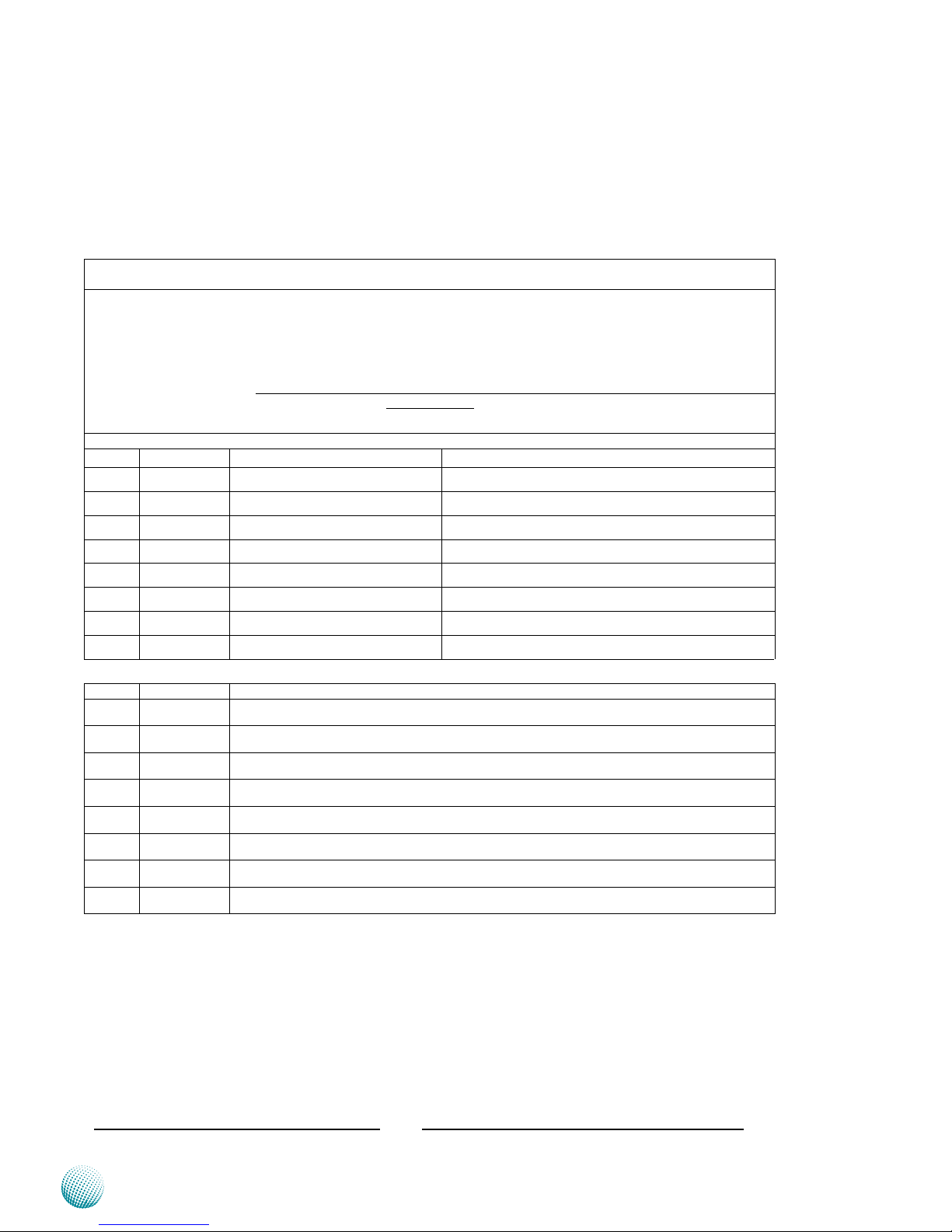
RMA Service Request Form
When requesting RMA service, please fill out the following form. Without
this form enclosed, your RMA cannot be processed.
RMA No:
Reasons to Return: Ŀ Repair(Please include failure details)
Ŀ Testing Purpose
Company: Contact Person:
Phone No. Purchased Date:
Fax No.: Applied Date:
Return Shipping Address:
Shipping by: Ŀ Air Freight Ŀ Sea Ŀ Express ___
Ŀ Others:________________
Item Model Name Serial Number Configuration
Item Problem Code Failure Status
*Problem Code:
01:D.O.A.
02: Second Time
R.M.A.
03: CMOS Data Lost
04: FDC Fail
05: HDC Fail
06: Bad Slot
07: BIOS Problem
08: Keyboard Controller Fail
09: Cache RMA Problem
10: Memory Socket Bad
11: Hang Up Software
12: Out Look Damage
13: SCSI
14: LPT Port
15: PS2
16: LAN
17: COM Port
18: Watchdog Timer
19: DIO
20: Buzzer
21: Shut Down
22: Panel Fail
23: CRT Fail
24: Others (Pls specify)
Request Party
Confirmed By Supplier
Authorized Signature / Date Authorized Signature / Date
 Loading...