

Page 1
Densitron Technologies plc does not warrant the accuracy or completeness of the information contained herein, the supply of products by
Densitron is subject to its standard terms and conditions of sale.
Page 2
Densitron Technologies plc does not warrant the accuracy or completeness of the information contained herein, the supply of products by
Densitron is subject to its standard terms and conditions of sale.
Caution
1. This Kyocera LCD module has been specifically designed for use only
in electronic devices in the areas of audio control, office automation,
industrial control, home appliances, etc. The modules should not be
used in applications where module failure could result in physical harm
or loss of life, and Kyocera expressly disclaims any and all liability
relating in any way to the use of the module in such applications.
2. Customer agrees to indemnify, defend and hold Kyocera harmless from
and against any and all actions, claims, losses, damages, liabilities,
awards, costs, and expenses, including legal fees, resulting from or
out of Customer's use, or sale for use, of Kyocera modules inarising
applications.
3. Kyocera shall have the right, which Customer hereby acknowledges, to
immediately scrap or destroy tooling for Kyocera modules for which no
Purchase Orders have been received from the Customer in a two-year
period.
Page 3
Densitron Technologies plc does not warrant the accuracy or completeness of the information contained herein, the supply of products by
Densitron is subject to its standard terms and conditions of sale.
Page 4
1.Application
This data sheet defines the specification for a (320×R.G.B)×240 dot, STN Transflective
color dot matrix type Liquid Crystal Display with CFL backlight.
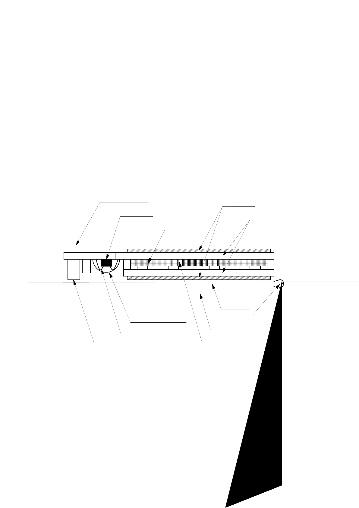
2.Construction and Outline
(320×R.G.B)×240 dots, COB type LCD with CFL backlight.
Backlight system : Side-edge type CFL (1 tube).
Inverter : Option
Recommended Inverter : PH-BLC08-K3 (HITACHI MEDIA ELECTRONICS)
or equivalent
Polarizer : Glare treatment.
Additional circuit : Bias voltage circuit, Randomizing circuit.
Backlight case
Driver IC
Protective resin
Au wire
Additional circuit
Color filter
B
GR
Polarizer
RBGR
Diffuser
Backlight case
Liquid crystal
Glass
BGRBG
CFL tube
This drawing is showing conception only.
-1-
Page 5
Densitron Technologies plc does not warrant the accuracy or completeness of the information contained herein, the supply of products by
Densitron is subject to its standard terms and conditions of sale.
3.Mechanical Specifications
Outline dimensions 154.6 (W) × 114.8 (H) × 8.5 (D) mm
Effective viewing area 118.18 (W) × 89.38 (H) mm
Dot number (320×R.G.B) (W) × 240 (H) Dots
Dot size 0.10 (W) × 0.34 (H) mm
Dot pitch 0.12 (W) × 0.36 (H) mm
Display color *1 White *2 -
Base color *1 Black *2 -
Mass 200 g
*1 Due to the characteristics of the LC material, the color vary with environmental temperature.
*2 Negative-type display
Display data "H" :R.G.B Dots ON : White
Display data "L" :R.G.B Dots OFF : Black
ITEM SPECIFICATION UNIT
4.Absolute Maximum Ratings
4-1. Electrical absolute maximum ratings
ITEM SYMBOL MIN. MAX. UNIT
Supply voltage for logic VDD 0 7.0 V
Supply voltage for LCD driving VEE 0 33.0 V
Input signal voltage *1 Vin 0 VDD V
*1 Input signal : CP,LOAD,FRM,DISP,D0~D7
-2-
Page 6
Densitron Technologies plc does not warrant the accuracy or completeness of the information contained herein, the supply of products by
Densitron is subject to its standard terms and conditions of sale.
4-2. Environmental absolute maximum ratings
ITEM SYMBOL MIN MAX UNIT
Operating temperature *1 Top 0 50 ℃
Storage temperature *2 T -20 60 ℃
STO
Operating humidity *3 Hop 10 *4 %RH
Storage humidity *3 H 10 *4 %RH
STO
Vibration - *5 *5 -
Shock - *6 *6 -
*1 LCD's display quality shall not be guaranteed at the temperature range of : below 0℃
and upper 40℃
*2 Temp. = -20℃<48 h , Temp = 60 ℃<168 h
Store LCD panel at normal temperature/humidity. Keep it free from vibration and shock.
LCD panel that is kept at low or high temperature for a long time can be defective due
to the other conditions, even if the temperature satisfies standard.
*3 Non-condensation.
*4 Temp. ≦ 40℃,85% RH Max.
Temp. > 40℃, Absolute Humidity shall be less than 85%RH at 40℃.
*5
Frequency 10~55 Hz Converted to
acceleration value :
Vibration width 0.15 mm (0.3~9m/s )
2
Interval 10-55-10 Hz 1 minute
2 hours in each direction X/Y/Z (6 hours as total)
EIAJ ED-2531.
*6 Acceleration: 490m/s
2
Pulse width : 11 ms
3 times in each direction : ±X/±Y/±Z.
EIAJ ED-2531.
-3-
Page 7
Densitron Technologies plc does not warrant the accuracy or completeness of the information contained herein, the supply of products by
Densitron is subject to its standard terms and conditions of sale.
5.Electrical Characteristics
ITEM SYMBOL CONDITION MIN. TYP. MAX. UNIT
Supply voltage for logic VDD - 4.75 5.00 5.25 V
LCD driving voltage *1 0 ℃ (25.0) (26.0) (27.0) V
Input voltage Vin "H" level 0.8VDD - VDD V
Clock frequency fcp - 2.02 2.16 16.0 MHz
Frame frequency *2 f-70 75 - Hz
Current consumption IDD - (3.0) (4.5) mA
for logic
Current consumption IEE *3 - (7.5) (11.3) mA
for LCD driving
Power consumption Pdisp - (210) (330) mW
Vop=
VEE 25 ℃ (24.6) (25.6) (26.6) V
50 ℃ (23.6) (24.6) (25.6) V
"L" level 0 - 0.2VDD V
FRM
VDD = +5.0V ± 5%, Temp. = 0~50℃
*1 Maximum contrast ratio is obtained by adjusting the LCD supply voltage( Vop= VEE ) for
driving LCD.
*2 In consideration of display quality, it is recommended that frame frequency is set in
the range of 70-80Hz. When you have to use higher frame and clock frequencies, confirm
the LCD's performance and quality prior to finalizing the frequency values: Generally,
as frame and clock frequencies become higher,current consumption will get bigger and
display quality will be degraded.
*3 Display high frequency pattern, ( see below ).
VDD = 5.0V , Vop = VEE , f = 75 Hz , fcp = 2.16MHz , Temp. = 25℃
FRM
Pattern:
1 2 3 4 5 6 960(dot)
1
■□■□■□■□■□■□■□■□■□■□
2
□■□■□■□■□■□■□■□■□■□■
3
■□■□■□■□■□■□■□■□■□■□
□■□■□■□■□■□■□■□■□■□■
:
■□■□■□■□■□■□■□■□■□■□
:
□■□■□■□■□■□■□■□■□■□■
239
■□■□■□■□■□■□■□■□■□■□
240
(dot)
-4-
Page 8

Densitron Technologies plc does not warrant the accuracy or completeness of the information contained herein, the supply of products by
Densitron is subject to its standard terms and conditions of sale.
6.Optical Characteristics
6-1. Reflective mode
ITEM SYMBOL CONDITION MIN. TYP. MAX. UNIT
Response Rise Tr θ=φ=0°-(200) (300) ms
time
Down Td θ=φ=0°-(150) (250) ms
Contrast ratio CR θ=φ=0° (4.0) (8.0) --
Reflectance ρ-(2.5) (5.0) - %
Optimum contrast is obtained by adjusting the LCD driving voltage(Vop) while at the viewing
angle of θ = φ =0°.
6-2. Transmimissive mode
Measuring Spot = φ6mm , Temp. = 25℃
Measuring Spot = φ6mm , Temp. = 25℃
ITEM SYMBOL CONDITION MIN. TYP. MAX. UNIT
Response Rise Tr θ=φ=0°-(200) (300) ms
time
Down Td θ=φ=0°-(150) (250) ms
Viewing angle range θφ=0゜ (-30) - (40) deg.
CR≧2
φθ=0゜ (-50) - (50) deg.
Contrast ratio CR θ=φ=0° (15.0) (30.0) --
Brightness (IL=5mA) L - (90) (130) - cd/㎡
Chromaticity Red x (0.39) (0.44) (0.49)
coordinates θ=φ=0°
y (0.28) (0.33) (0.38)
Green x (0.27) (0.32) (0.37)
θ=φ=0°
y (0.36) (0.41) (0.46)
Blue x (0.17) (0.22) (0.27)
θ=φ=0°-
y (0.15) (0.20) (0.25)
White x (0.26) (0.31) (0.36)
θ=φ=0°
y (0.26) (0.31) (0.36)
Optimum contrast is obtained by adjusting the LCD driving voltage(Vop) while at the viewing
angle of θ = φ =0°.
-5-
Page 9
Densitron Technologies plc does not warrant the accuracy or completeness of the information contained herein, the supply of products by
Densitron is subject to its standard terms and conditions of sale.
6-3. Definition of Reflectance
6-4. Definition of Contrast (Reflective Mode)
ρ(Reflectance) = × 100[%]
Reflection Brightness against Standard White Board
Measured Reflection Brightness
CR(Contrast) =
Reflectance at all pixels "White"
Reflectance at all pixels "Black"
6-5. Definition of Contrast (Transmissive Mode)
Brightness at all pixels "White"
CR(Contrast) =
Brightness at all pixels "Black"
6-6. Definition of Vop
C
C
o
o
CC
n
n
r
t
oo
r
t
a
nn
a
t
s
rr
tt
t
s
aa
tt
ss
x
x
C
C
R
R
m
m
a
a
xx
CC
RR
mm
aa
VVVVEEEEEEEE((((VVVV))))
VVVVoooopppp
-6-
Page 10

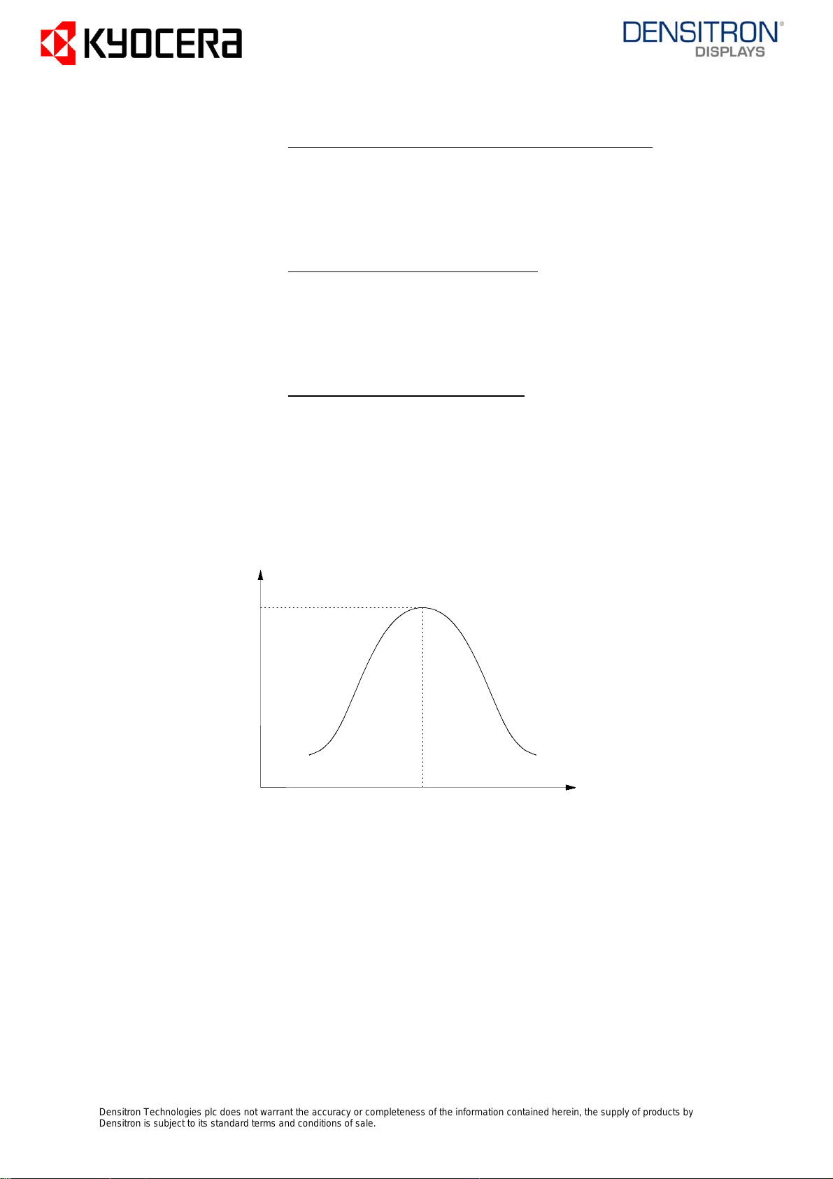
6-7. Definition of response time
6-8. Definition of viewing angle
-7-
Page 11

Densitron Technologies plc does not warrant the accuracy or completeness of the information contained herein, the supply of products by
Densitron is subject to its standard terms and conditions of sale.
6-9. Measuring points
80×3 160×3 240×3 (dot)
14
60 ○○
3
120 ○
25
180 ○○
(dot)
1) Rating is defined as the average brightness inside the viewing area.
2) 30 minutes after CFL is turned on. (Ambient Temp.=25℃)
3) The inverter should meet the eccentric conditions;
-Sine, symmetric waveform without spike in positive and negative.
4) Measuring Inverter : PH-BLC-08-K3(HITACHI MEDIA ELECTRONICS)
6-10. Measurement method of reflectance
Direction of detection light
Y
Direction of incident light
-
X
+
θ
θ=25°
-
Y
+X
-8-
Page 12

Densitron Technologies plc does not warrant the accuracy or completeness of the information contained herein, the supply of products by
Densitron is subject to its standard terms and conditions of sale.
7. Circuit Block Diagram
1/240 duty
SEGMENT DRIVER IC
D0 ~D7
CP
*1
LOAD
DISP
VDD,VSS
COMMON DRIVER IC
FRM
(320×R.G.B)×240 LCD
SEG
IC
VEE *2
*2 Bias voltage circuit
*1 Randomizing circuit
IC
COM
-9-
Page 13

Densitron Technologies plc does not warrant the accuracy or completeness of the information contained herein, the supply of products by
Densitron is subject to its standard terms and conditions of sale.
7-1.Power supply
VR
Tr
VEE
Vop KHS057QV1C
+5.0V VDD
VSS
-10-
Page 14

Densitron Technologies plc does not warrant the accuracy or completeness of the information contained herein, the supply of products by
Densitron is subject to its standard terms and conditions of sale.
8.Interface signals
8-1.LCD
CN1 : 53261-1510(Molex)
PIN NO. SYMBOL DESCRIPTION LEVEL
1 FRM Synchronous signal for driving scanning line H
2 LOAD Data signal latch clock H → L
3 CP Data signal shift clock H → L
4 DISP Display control signal H(ON),L(OFF)
5 VDD Power supply for logic ―
6 VSS GND ―
7 VEE Power supply for LCD ―
8D7
9 D6 Display data
10 D5
11 D4 H(ON),L(OFF)
12 D3
13 D2
14 D1
15 D0
Recommended matching connector :51021-1500(Molex)
This pin assignment is the reverse of what Molex defined.
Remember that for you designing.
8-2. CFL
PIN No SYMBOL DESCRIPTION
1 HOT Inverter output high voltage side
2 NC No connect
3 COLD Inverter output low voltage side
LCD side connector : BHR-03VS-1 (JST)
Recommended matching connector : SM02-(8.0)B-BHS-1 (JST)
-11-
Page 15

Densitron Technologies plc does not warrant the accuracy or completeness of the information contained herein, the supply of products by
Densitron is subject to its standard terms and conditions of sale.
9.Interface Timing Chart
LOAD
CP
D7 G318 R1 B3 G318 R1
D6 B318 G1 R4 B318 G1
D5 R319 B1 G4 R319 B1
D4 G319 R2 B4 G319 R2
D3 B319 G2 R5 B319 G2
D2 R320 B2 G5 R320 B2
D1 G320 R3 B5 G320 R3
D0 B320 G3 R6 B320 G3
FRM
CP × (320×R.G.B) / 8 pulse
LOAD
×1 ×2 ×240 ×1
D0~D7
FRM
* The cycle of load signal should be stable and continuously applied without interruption.
* The above-mentioned timing chart shows a reference to set up a LCD module, not an electrical
rating.
-12-
Page 16

Densitron Technologies plc does not warrant the accuracy or completeness of the information contained herein, the supply of products by
Densitron is subject to its standard terms and conditions of sale.
10.Data and Screen
CHIP AREA
Y1 Y2 Y3 ・・・ Y320
CX1
H D7D6D5D4D3D2D1D0D7 D2D1D0
I R1 G1 B1 R2 G2 B2 R3 G3 B3 R320 G320 B320
P
A
R
E
A
X240
-13-
Page 17

Densitron Technologies plc does not warrant the accuracy or completeness of the information contained herein, the supply of products by
Densitron is subject to its standard terms and conditions of sale.
11.Input Timing Characteristics
trCP tfCP
tWCLH tWCLL tCCL
CP
tDS tDH
DATA
CP
LOAD
FRM
last 1st 1st
tCL tLC
tWLPH
tLCL
tWLPL
tr tf
tFS tFH
-14-
Page 18

Densitron Technologies plc does not warrant the accuracy or completeness of the information contained herein, the supply of products by
Densitron is subject to its standard terms and conditions of sale.
11-1.Switching characteristics
ITEM SYMBOL MIN. MAX. UNIT
CP Cycle *1,*2 tCCL 62 - ns
CP "H" Pulse Width *2 tWCLH 25 - ns
CP "L" Pulse Width *2 tWCLL 25 - ns
CP Rise Up Time *2 trCP - 30 ns
CP Fall Down Time *2 tfCP - 30 ns
Data Set Up Time tDS 20 - ns
Data Hold Time tDH 15 - ns
LOAD "H" Pulse Width tWLPH 50 - ns
LOAD "L" Pulse Width tWLPL 370 - ns
Input characteristics; VDD = +5.0V ± 5% Temp. = 25 ℃
LOAD Cycle *3 tLCL 420 - ns
CP→LOAD Delay Time tCL 0 - ns
LOAD→CP Delay Time *4 tLC 120-tWLPH - ns
Input Signal Rise Up Time tr - 30 ns
Input Signal Fall Down Time tf - 30 ns
FRM Data Set Up Time tFS 100 - ns
FRM Data Hold Time tFH 30 - ns
*1 CP Cycle is adjust so that FRM signal is 75Hz.
*2 The formula of condition
①trCP + tfCP ≦ tCCL - ( tWCLH + tWCLL )
②trCp,tfCp ≦ 30ns
Please use on condition that ①,② are filled.
*3 LOAD Cycle is const.
*4 tLC ≧ 0
-15-
Page 19

12.Supply Voltage Sequence Condition
DO NOT apply DC voltage to the LCD panel. DC voltage induce irreversible electrochemical
reactions and reduce LCD life. Always follow the power supply ON/OFF sequence of VDD first,
input signal second, VEE third and finally DISP. This will prevent DC driving of the LCD or
CMOS LSI latch up as shown below.
1s MIN. 1s MIN.
VDD
0~50ms
0~50ms
Input signal
0~100ms 100ms MIN.
VEE
DISP
0s MIN. 0s MIN.
* Input signal : CP, LOAD, FRM, D0~D7
* The above sequence should be designed as to keep each normal figure on condition that
liquid crystal module is loaded on your system.
* Control the input signal and VEE to the above ON - OFF timing when you switch ON/OFF
the display during VDD and DISP are on.
And also design the circuit as VEE's OFF level become GND level.
* Control the supply voltage sequence not to float all signal line when the LCD panel is
driving.
-16-
Page 20

Densitron Technologies plc does not warrant the accuracy or completeness of the information contained herein, the supply of products by
Densitron is subject to its standard terms and conditions of sale.
13 .Backlight Characteristics
Temp.= 25℃
ITEM SYMBOL MIN. TYP. MAX. NOTE
Starting discharge Voltage --790 Vrms. 0 ℃
*1 VS
--525 Vrms. 25 ℃
Discharging tube current *2,*3 IL 2.0 mArms. 5.0 mArms. 6.0 mArms. -
Discharging tube voltage VL - 320 Vrms. --
Operating life *4 T 25,000 h 40,000 h --
(IL=5.0 mArms.)
Operating frequency F 30 kHz - 100 kHz -
*1 The Non-load output voltage (VS) of the inverter should be designed to have some margin,
because VS may increase due to the leak current which may becaused by wiring of CFL cables.
(Reference value: 1030 Vrms MIN.)
*2 We recommend that you should set the discharging tube current at lower than typical value
so as to prevent the heat accumulation of CFL tube from deteriorating a performance of the
LCD.
*3 Do not apply more than 6.0mA discharging tube current. Because CFL maybe broken due to over
current.
*4 When the illuminance or quantity of light has decreased to 50% of the initial value.
Average life time of CFL will be decreased when LCD is operating at lower and higher
temperature.
-17-
Page 21

Densitron Technologies plc does not warrant the accuracy or completeness of the information contained herein, the supply of products by
Densitron is subject to its standard terms and conditions of sale.
14.Lot Number Identification
The lot number shall be indicated on the back of the backlight case of each LCD.
KHS057QV1CJ-G01- □ □-□ □
DATE
MONTH
YEAR
YEAR 2004 2005 2006 2007 2008 2009
CODE 456789
MONTH JAN. FEB. MAR. APR. MAY JUN.
CODE 123456
MONTH JUL. AUG. SEP. OCT. NOV. DEC .
CODE 789XYZ
15.Warranty
15-1. Incoming inspection
Please inspect the LCD within one month after your receipt.
15-2. Production Warranty
Kyocera warrants its LCDs for a period of 12 months after receipt by the purchaser, and
within the limits specified. Kyocera shall, by mutual agreement, replace or rework defective
LCDs that are shown to be Kyocera's responsibility.
-18-
Page 22

Densitron Technologies plc does not warrant the accuracy or completeness of the information contained herein, the supply of products by
Densitron is subject to its standard terms and conditions of sale.
16.Precautions for use
16-1. Installation of the LCD
1. Please ground either of the mounting(screw) holes located at each corner of an LCD module,
in order to stabilize brightness and display quality.
2. A transparent protection plate shall be added to protect the LCD and its polarizers.
3. The LCD shall be installed so that there is no pressure on the LSI chips.
4. The LCD shall be installed flat, without twisting or bending.
5. The display window size should be the same as the effective viewing area.
6. In case you use outside frame of effective viewing area as outward appearance of your product,
unevenness of its outward appearance is out of guarantee.
7. Do not pull the CFL lead wires and do not bend the root of the wires. Housing should be
designed to protect CFL lead wires from external stress.
8. This Kyocera LCD module has been specifically designed for use in general electronic devices,
but not for use in a special environment such as usage in an active gas.
Hence, when the LCD is supposed to be used in a special environment, evaluate the LCD
thoroughly beforehand and do not expose the LCD to chemicals such as an active gas.
16-2. Static Electricity
1. Since CMOS ICs are mounted directly onto the LCD glass, protection from static electricity is
required. Operation should wear ground straps.
16-3. LCD Operation
1. The LCD shall be operated within the limits specified. Operation at values outside of these
limits may shorten life, and/or harm display images.
2. Adjust "LCD driving voltage" to obtain optimum viewing angle and contrast.
3. Operation of the LCD at temperature below the limit specified may cause image degradation
and/or bubbles. It may also change the characteristics of the liquid crystal.
This phenomenon may not recover. The LCD shall be operated within the temperature limits
specified.
16-4. Storage
1. The LCD shall be stored within the temperature and humidity limits specified. Store in
a dark area, and protected the LCD from direct sunlight or fluorescentlight.
2. The LCD should be packaged to prevent damage.
16-5. Screen Surface
1. DO NOT store in a high humidity environment for extended periods. Image degradation, bubbles,
and/or peeling off of polarizer may result.
2. The front polarizer is easily scratched or damaged. Prevent touching it with any hard
material, and from being pushed or rubbed.
3. The LCD screen may be cleaned with a soft cloth or cotton pad. Methanol, or Isopropyl
Alcohol may be used, but insure that all solvent residue is removed.
4. Water may cause damage or discoloration of the polarizer. Clean any condensation or moisture
from any source immediately.
5. Always keep the LCD free from condensation during testing. Condensation may permanently spot
or stain the polarizers.
-19-
Page 23

Densitron Technologies plc does not warrant the accuracy or completeness of the information contained herein, the supply of products by
Densitron is subject to its standard terms and conditions of sale.
17.Reliability Data / Environmental Test
TEST ITEM TEST CONDITION TEST TIME RESULT
High Temp. Display Quality : No defect
60℃ 240 h Display Function : No defect
Atmosphere Current Consumption : No defect
Low Temp. Bubble : None
Low Temp. Solid Crystallization of
-20℃ 240 h Liquid Crystal : None
Atmosphere Display Quality : No defect
Display Function : No defect
Current Consumption : No defect
High Temp. Display Quality : No defect
40℃ Display Function : No defect
Humidity 240 h Peel-off of Organic Sealing
90%RH : None
Atmosphere Current Consumption : No defect
-20℃ 0.5 h Display Quality : No defect
Display Function : No defect
Temp. Cycle R.T. 0.5 h 10cycles Peel-off of Organic Sealing
:None
60℃ 0.5 h Bubble on Cell : None
High Temp. 50℃ 500 h Display Quality : No defect
Operation Vop Current Consumption : No defect
* Each test item uses a test LCD only once. The tested LCD is not used in any other tests.
* The LCD is tested in circumstances in which there is no condensation.
* The tested LCD is inspected after 24 hours of storage at room temperature and room humidity
after each test is finished.
* The reliability test is not an out-going inspection.
* The results of the reliability test are for your reference purpose only.
The reliability test is conducted only to examine the LCD's capability.
-20-
Page 24

Page 25

Densitron Technologies plc does not warrant the accuracy or completeness of the information contained herein, the supply of products by
Densitron is subject to its standard terms and conditions of sale.
Page 26

Densitron Technologies plc does not warrant the accuracy or completeness of the information contained herein, the supply of products by
Densitron is subject to its standard terms and conditions of sale.
Date
Rev. No. Date Page Descriptions
Designed by: Engineering Dept. Confirmed by: QA Dept.
Prepared Checked Approved Checked Approved
Revision Record
Page 27

Densitron Technologies plc does not warrant the accuracy or completeness of the information contained herein, the supply of products by
Densitron is subject to its standard terms and conditions of sale.
Visuals specification
1)Note
Item Note
General 1.When defects specified in th is Inspection Standards are
inspected, o perating voltage(Vop ) shall be set at the
level where optimized contrast is available.
Display qual ity is applied up to effective viewi ng area.
(Bi-Level INSPEC TION)
2.This inspect ion standard about t he image quality shall be
applied to any defect within the effective viewi ng area
and shall not be applicable to outside of the ar ea.
3.Should any defects which are not specified in this
standard hap pen, additional standard shall be determined
by mutual agreement between customer and Kyocera.
4.Inspection c onditions
Luminance : 500 Lux mi nimum .
Inspection d istance : 300 mm (from the sample)
Temperature : 25 ± 5 ℃
Direction : right above
Definition of Inspection Pinhole, Brigh t spot The color of a small area is
item Black spot, Scratch diff erent from the remainder.
Foreign partic le The phenomeno n does not chang e
with voltage.
Contrast varia tion The color of a small are a is
different fro m the remainder.
The phenomeno n changes with
voltage.
Polarizer ( Scratch, Scratch, Bubble and Dent in the
Bubble, Dent ) polarizer which ca n be o bserved
in on / off state.
-1-
Page 28

Densitron Technologies plc does not warrant the accuracy or completeness of the information contained herein, the supply of products by
Densitron is subject to its standard terms and conditions of sale.
2)Standard
Inspection item Judgement sta ndard
Pinhole, Bright spot
Black spot,
Foreign particl e
Scratch,Foreign particle
b
a
d=(a+b)/2
Category Size (mm) Acceptable numb er
Ad≦ 0.2 neglected
B 0.2 < d ≦ 0.3 5
C 0.3 < d ≦ 0.5 3
D 0.5 < d0
Contrast variat ion
W
L
Width (mm) Length (mm) Acceptable No.
AW≦ 0.03 neglected
BL≦ 2.0 neglected
C 0.03< W ≦ 0.1 2.0 < L ≦ 4.0 3
D 4.0 < L0
E 0.1 < W According to
' Circular '
b
a
Category Size (mm) Acceptable number
Ad≦ 0.5 neglected
B 0.5 < d ≦ 0.7 3
C 0.7 < d0
-2-
d=(a+b)/2
Page 29

Densitron Technologies plc does not warrant the accuracy or completeness of the information contained herein, the supply of products by
Densitron is subject to its standard terms and conditions of sale.
Inspection item Judgement sta ndard
Polarizer ( Scratch, (1) Scratch W
Bubble, Dent )
L
Width (mm) Length (mm) Acceptable No.
AW≦ 0.1 neglected
BL≦ 5.0 neglected
0.1 < W ≦ 0.3
C 5.0 < L0
D 0.3 < W0
(2)Bubble ( dent )
b
a
d=(a+b)/2
Category Size (mm) Acceptable number
Ad≦ 0.2 neglected
B 0.2 < d ≦ 0.3 5
C 0.3 < d ≦ 0.5 3
D 0.5 < d0
-3-
 Loading...