Kenwood TM-V71E, TM-V71A Service Manual
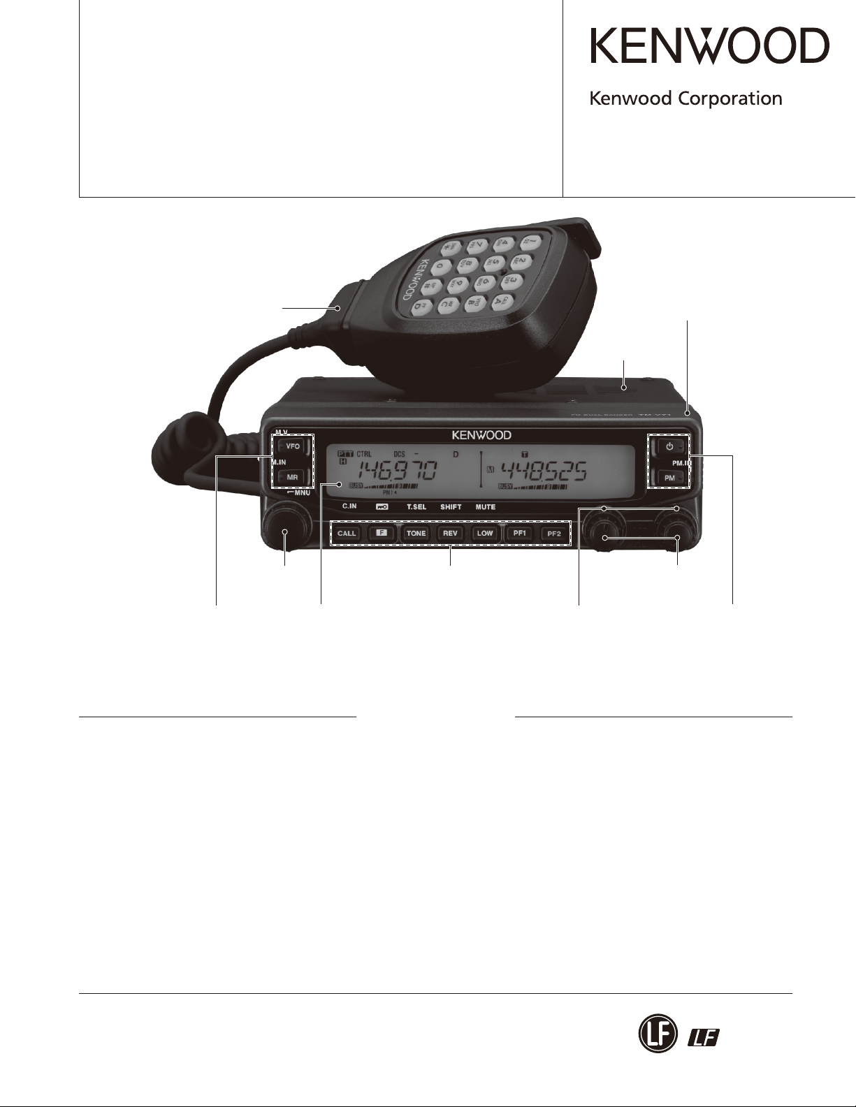
144/430 (440) MHz FM DUAL BANDER
TM-V71A/V71E
SERVICE MAN UAL
© 2007-5 PRINTED IN JA PA N
B51-8791-00 (N) 289
Button knob (VFO,MR)
(K29-9378-03)
Photo is TM-V71A.
Microhone
(T91-0657-15)
Knob (ENC)
(K29-9376-03)
Button knob (7KEYS)
(K29-9381-02)
Front glass (Display)
(B10-2775-12)
Metallic cabinet
(A01-2206-02)
Knob (SQL)
(K29-9380-03) x 2
Panel (Display)
(A62-1135-03)
Knob (VOL)
(K29-9377-03) x 2
Button knob (POWER,PM)
(K29-9379-03)
CONTENTS
DISASSEMBLY FOR REPAIR ......................2
CIRCUIT DESCRIPTION ..............................3
SEMICONDUCTOR DATA .........................11
COMPONENTS DESCRIPTION .................14
TERMINAL FUNCTION .............................19
PARTS LIST ...............................................22
EXPLODED VIEW ......................................38
PACKING ....................................................39
ADJUSTMENT ..........................................40
PC BOARD
DISPLAY UNIT (X54-3590-00) ...............60
TX-RX UNIT (X57-731X-XX) .................64
INTERCONNECTION DIAGRAM ..............72
SCHEMATIC DIAGRAM ............................74
BLOCK DIAGRAM .....................................86
LEVEL DIAGRAM ...................................... 88
OPTIONAL ACCESSORIES .......................90
SPECIFICATIONS ......................................91
This product uses Lead Free solder.This product complies with the RoHS directive for the European market.
TM-V71A/V71E
Document Copyrights
Copyright 2007 by Kenwood Corporation. All rights
reserved.
No part of this manual may be reproduced, translated,
distributed, or transmitted in any form or by any means,
electronic, mechanical, photocopying, recording, or
otherwise, for any purpose without the prior written
permission of Kenwood.
DISASSEMBLY FOR REPAIR
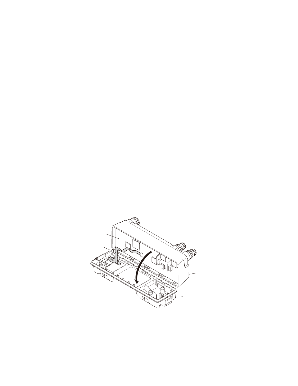
Precautions for Disassembly
When removing the rear case from the panel, open the
bottom side slowly so as not to stress the FPC, as the FPC
on the rear case is connected with the connector of the
display PCB.
Disclaimer
While every precaution has been taken in the preparation
of this manual, Kenwood assumes no responsibility for
errors or omissions. Neither is any liability assumed for
damages resulting from the use of the information contained
herein. Kenwood reserves the right to make changes to any
products herein at any time for improvement purposes.
Display PCB
FPC
Panel
Rear case
2
CIRCUIT DESCRIPTION
TM-V71A/V71E
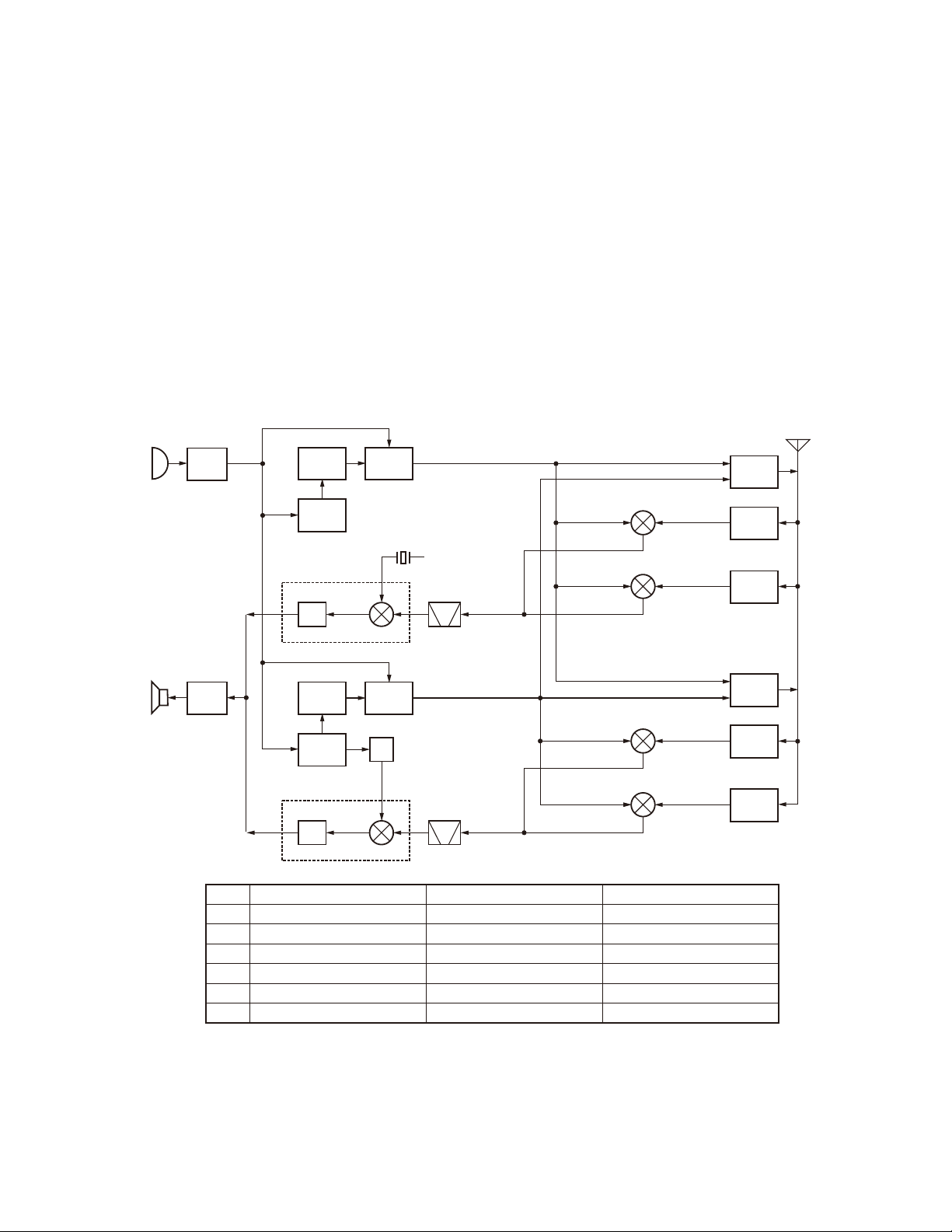
1. Frequency Confi guration
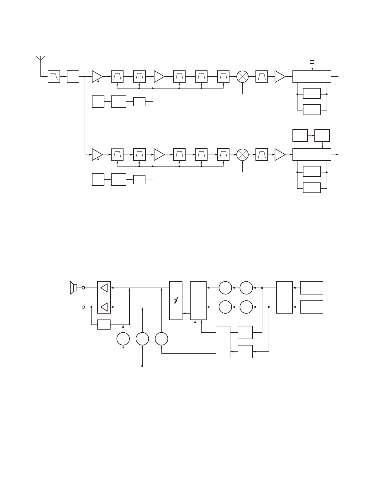
The TM-V71A/V71E has an individual VCO and PLL unit
for both band A and band B. Using these separate VCO and
PLL circuits, it can receive 2 separate bands at the same
time. You can also perform full-duplex operation.
The band A VCO is used for the following functions:
(i) VHF/UHF transmission
(ii) The first local oscillator for the band A (VHF)
reception.
(iii) The first local oscillator for the band A (UHF)
reception.
The band B VCO is used for the following functions:
(i) VHF/UHF transmission
(ii) The first local oscillator for the band B (VHF)
reception.
MIC
MIC
AMP
PLL A VCO A
TCXO
12.8MHz
FM IC
2dn IF
455kHz
DET
45.505MHz
MCF
45.05MHz
(iii) The first local oscillator for the band B (UHF)
reception.
The PLL reference frequency is generated by a 12.8MHz
(band A) and a 16.8MHz (band B) crystal oscillator connected
to the band A and band B PLL ICs. This reference frequency
is used for both PLL circuits. The 45.505MHz second local
oscillator for band A is generated by the FM IC crystal
oscillator circuit. The second local oscillator for the band B
uses the tripled 16.8MHz reference oscillator frequency.
Note:
The PCB layout and the mounting parts are the same for the
band A VCO (X57-731 B/6) and band B VCO (X57-731 C/6),
although the PCB silk print is different.
ANT
A
VHF TX
C
D
1st IF
45.05MHz
A
B
Band A
VHF RX
Band A
UHF RX
SP
AF
AMP
A 144.000 ~147.995MHz 144.000~145.995MHz 144.000~145.995MHz
B 438.000~449.995MHz 430.000~439.995MHz 430.000~439.995MHz
C 189.050~193.045MHz 189.050~191.045MHz 189.050~191.045MHz
D 392.950~404.945MHz 384.950~394.945MHz 384.950~394.945MHz
E 193.950~197.945MHz 193.950~195.945MHz 193.950~195.945MHz
F 388.050~400.045MHz 380.050~390.045MHz 380.050~390.045MHz
PLL B
TCXO
16.8MHz
FM IC
DET
K type E type M4 type
2dn IF
450kHz
VCO B
x3
50.4MHz
MCF
49.95MHz
E
F
1st IF
49.95MHz
Fig. 1 Frequency confi guration
B
A
B
UHF TX
Band B
VHF RX
Band B
UHF RX
3
TM-V71A/V71E
CIRCUIT DESCRIPTION
2. Receiver System
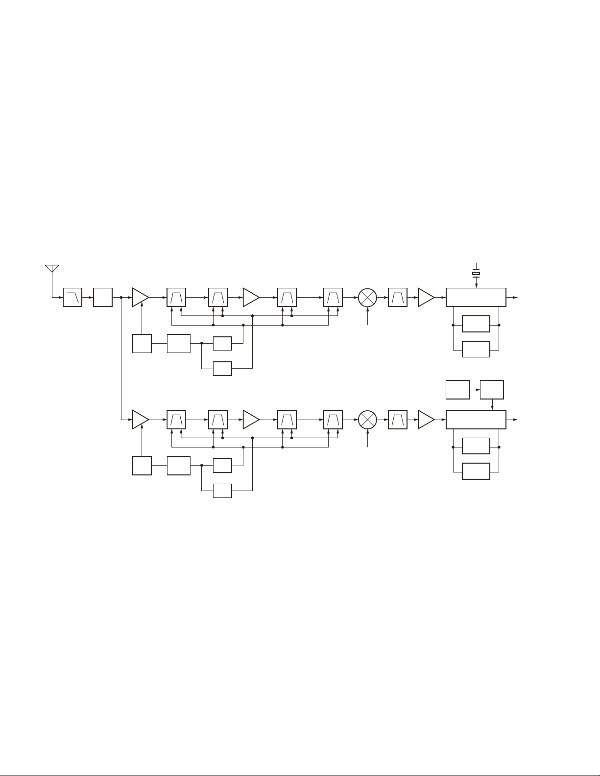
2-1. Band A VHF Receiver Circuit
The incoming signal from the antenna passes through
a filter circuit and goes to the RF amplifier (Q228). The
amplifi ed signal enters the band-pass fi lter. After the signal
passes through the band-pass fi lter, it is amplifi ed by another
RF amplifier (Q227) and then passes through the bandpass fi lter before entering the mixer (Q226). The frequency
of the signal is converted by the fi rst local oscillator (Upper
heterodyne) to generate a 45.05MHz first IF signal. The
signal passes through the MCF (XF486), is amplifi ed by the
IF amplifi er (Q495) and then enters the FM IC (IC486).
The signal is converted to the 455kHz second IF signal
by the second local oscillator (Upper heterodyne). It is then
detected to generate an audio signal.
BPF
D238~240
L245,257
IC667
D/A
IC576
SW
BPF
D303~305
L309,310,322
IC667
D/A
IC577
SW
RF AMP
Q227
RF AMP
Q292
D232~234
L232,236,250
D297~299
L301,302,323
LPF
D134,135
D186,188
ANT
SW
RF AMP
Q228
AIP
SW
IC576
Q229
RF AMP
Q293
AIP
SW
IC576
Q294
BPF
D241~243
L248,249,258
MPU
IC918
BPF
D306~308
L312~314
MPU
IC918
2-2. Band B VHF Receiver Circuit
The incoming signal from the antenna passes through
a filter circuit and goes to the RF amplifier (Q293). The
amplifi ed signal passes through the band-pass fi lter and is
amplified by another RF amplifier (Q292). It then passes
through the band-pass fi lter and goes to the mixer (Q291).
The frequency of the signal is converted by the fi rst local
oscillator (Upper heterodyne) to generate a 49.95MHz fi rst
IF signal. The signal passes through the MCF (XF546), is
amplified by the IF amplifier (Q551) and then enters the
FM IC (IC546). The signal is then converted to the 450kHz
second IF signal by the second local oscillator, which is
tripled 16.8MHz (Upper heterodyne). It is then detected to
generate an audio signal.
BPF
Band A
BPF
Band B
BPF
D229~231
L232,233,260
BPF
D294~296
L297,298,324
MIXER
Q226
1st Local OSC
MIXER
Q291
1st Local OSC
MCF
XF486
45.05MHz
MCF
XF546
49.95MHz
IF AMP
Q495
IF AMP
Q551
16.8MHz Q547
TCXO
X66
X486
45.505MHz
2nd Local OSC
FM IC
IC486
CF
Wide
CF
Narrow
Tripler
FM IC
IC546
CF
Wide
CF
Narrow
x3
2nd Local OSC
Band A
AF
Band B
AF
Fig. 2 Band A and Band B VHF receiver circuit
2-3. Band A UHF Receiver Circuit
The incoming signal from the antenna passes through
a filter circuit and goes to the RF amplifier (Q363). The
amplified signal enters the band-pass filter. After the
signal passes through the band-pass filter, it is amplified
by another RF amplifier (Q362) and then passes through
the band-pass filter before entering the mixer (Q361).
The frequency of the signal is converted by the fi rst local
oscillator (Lower heterodyne) to generate a 45.05MHz fi rst
IF signal. The signal passes through the MCF (XF486), is
amplifi ed by the IF amplifi er (Q495) and then enters the FM
IC (IC486). The signal is converted to the 455kHz second IF
signal by the second local oscillator (Upper heterodyne). It is
then detected to generate an audio signal.
4
2-4. Band B UHF Receiver Circuit
The incoming signal from the antenna passes through
a filter circuit and goes to the RF amplifier (Q408). The
amplifi ed signal passes through the band-pass fi lter and is
amplified by another RF amplifier (Q407). It then passes
through the band-pass fi lter and goes to the mixer (Q406).
The frequency of the signal is converted by the fi rst local
oscillator (Lower heterodyne) to generate a 49.95MHz fi rst
IF signal. The signal passes through the MCF (XF546), is
amplified by the IF amplifier (Q551) and then enters the
FM IC (IC546). The signal is then converted to the 450kHz
second IF signal by the second local oscillator, which is
tripled 16.8MHz (Upper heterodyne). It is then detected to
generate an audio signal.
The VHF/ UHF band-pass filter is tuned to the desired
frequency according to the BPF voltage output from the D/A
IC (IC667), and is controlled by the MPU (IC918) and the
varicap.
CIRCUIT DESCRIPTION
TM-V71A/V71E
LPF
D164,165
D187,189
ANT
SW
RF AMP
Q363
AIP
SW
IC576
Q400
RF AMP
Q408
AIP
SW
IC576
Q450
BPF
D378,379
L377
MPU
IC918
BPF
D423,424
L422
MPU
IC918
BPF
D375,376
L375
IC667
D/A
BPF
D420,421
L420
IC667
D/A
RF AMP
Q362
RF AMP
Q407
BPF
D370,371
L370
Band A
BPF
D415,416
L415
Band B
Fig. 3 Band A and Band B UHF receiver circuit
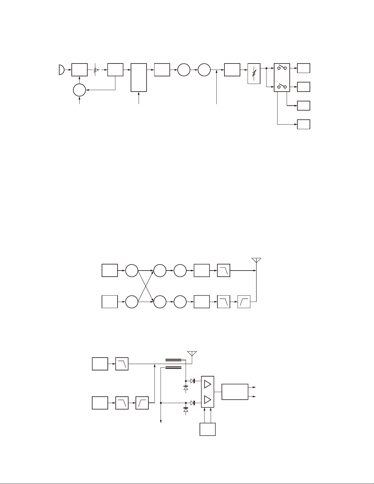
2-5. Audio Circuit
The detected band A audio signal is amplifi ed by Q810
and de-emphasized by Q806. The band B audio signal is
amplified by Q811 and de-emphasized by Q807. One of
these audio signals is selected with a cross point switch
(IC806). The signal passes through the electronic volume
BPF
D367,368
L368
BPF
D412,413
L413
BPF
D364,365
L366
BPF
D409,410
L411
MIXER
Q361
1st Local OSC
MIXER
Q406
1st Local OSC
MCF
XF486
45.05MHz
MCF
XF546
49.95MHz
IF AMP
Q495
IF AMP
Q551
16.8MHz Q547
TCXO
X66
X486
45.505MHz
2nd Local OSC
FM IC
IC486
CF
Wide
CF
Narrow
Tripler
FM IC
IC546
CF
Wide
CF
Narrow
x3
2nd Local OSC
(IC804), is amplifi ed by the AF amplifi er (IC801), and is then
fed to the speaker or the external speaker jack.
CTCSS and DCS signals that pass through the filter
circuit (IC805) go to the MPU (IC918) for CTCSS and DCS
decoding.
Band A
AF
Band B
AF
J801
(SP1)
J802
(SP2)
IC801
AF AMP
ATT
Q816
Q804 Q803
IC804
E VR
Fig. 4 Audio circuit
3. Transmitter System
3-1. Modulation Circuit
The audio modulation input from the microphone is
amplifi ed by IC802. After the DTMF signal and 1750Hz tone
signal generated by the MPU are switched with IC806, they
are mixed by IC803. After the signal amplified by IC802
is switched by IC806, it is amplifier by IC803. The signal
is then pre-emphasized by Q805 and Q808, and its level
is adjusted by IC804. The resulting signal goes to each of
DE-EMPHASIS A
IC486
FM IC (A)
IC546
FM IC (B)
IC806
Cross
Point
SW
MUTE1
MUTE2
BEEP
DTMF
Q806
Q807 Q811
DE-EMPHASIS B
IC918
MPU
Q810
IC805
1/2
IC805
1/2
CTCSS Filter AMP
IC666
Multi
SW
the band A and band B VCOs as a modulation signal. The
TONE/ DCS signal generated by the MPU is fed to IC803.
The signal amplifi ed by IC803 is distributed and the level is
adjusted by IC804. The modulating signal goes to each of
the band A and band B VCOs and the reference oscillation
circuit.
5
TM-V71A/V71E
CIRCUIT DESCRIPTION
MIC
MIC AMP
IC802
1/2
Q801
MUTE TONE/DCSDTMF
ALC AMP
IC802
1/2
ALC
IC806
Cross
Point
SW
1750Hz
PRE-EMPHASIS
IC803
1/2
Fig. 5 Modulation circuit
3-2. Transmitter Circuit
The VHF VCO output is amplifi ed by RF amplifi er (Q644)
and driver amplifi er (Q131). It is further amplifi ed to the fi nal
output by power module (IC131). The output signal passes
through antenna switch (D134, D135) and a low-pass fi lter,
and is then fed to the antenna.
The UHF VCO output is amplifi ed by RF amplifi er (Q161)
and driver amplifi er (Q162). It is further amplifi ed to the fi nal
output by power module (IC161). The signal passes through
antenna switch (D164, D165), and a low-pass and high-pass
fi lter, and is then fed to the antenna.
Q805
Q808
MOD AMP
IC803
2/2
IC804
E VR
IC807
TCXO (A)
X1
TCXO (B)
X66
VCO (A)
VCO (B)
3-3. APC Circuit
The Automatic transmission Power Control (APC) circuit
has a differential amplifier (IC187) that compares the DC
voltage generated by detecting part of the transmission
output using diodes (D191, D192) with the reference
voltage output from the D/A IC (IC667). The output signal is
switched by IC186 and is fed to the power module of each
VHF/UHF to keep transmission output constant.
IC131
Power
AMP
VHF
IC161
Power
AMP
UHF
VCO
A
VCO
B
LOCAL
AMP
Q7
LOCAL
AMP
Q72
LPF
LPF HPF
RF AMP
Q644
RF AMP
Q161
DRIVE
AMP
Q131
DRIVE
AMP
Q162
IC131
Power
AMP
VHF
IC161
Power
AMP
UHF
Fig. 6 Transmitter circuit
ANT
Reverse
Forward
VSF
to MPU
D192
D191
OP AMP
IC187
REV REFFWR REF
D/A
IC667
LPF
LPF HPF
Analog SW
IC186
ANT
APC V
APC U
Fig. 7 APC circuit
6
CIRCUIT DESCRIPTION
TM-V71A/V71E
3-4. Overheating Protection Circuit
To protect thermal destruction of the power modules
(IC131, IC161), the voltage of the thermistors (TH131,
TH161) near the power modules (IC131, IC161) is monitored
by the MPU (IC918). If their temperature becomes high,
this circuit reduces the APC voltage to cool down the
temperature.
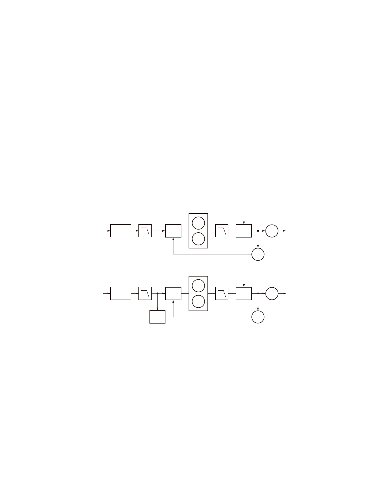
4. PLL Circuit
4-1. Reference Oscillator Circuit
Band A divides 12.8MHz inside the PLL IC (IC1) or band
B divides 16.8MHz inside the PLL IC (IC66) to generate a
5kHz or 6.25kHz reference frequency. The 16.8MHz signal
on IC66 side is tripled by Q547 to obtain the second local
oscillator for band B. The reference oscillation circuit is also
modulated to improve the modulation characteristics of the
DCS and 9600bps packet signal when it is transmitted.
4-2. Phase Comparator
Part of the band A VCO output is amplifi ed by Q5 and
goes to PLL IC (IC1). Also, a part of the band B VCO output
Band A
TCXO A
Mod Signal
X1
12.8MHz
TCXO
LPF LPF
PLL IC
IC1
is amplified by Q70 and goes to the PLL IC (IC66). The
pulse-swallow type PLL IC divides the input VCO oscillator
frequency using the data from the MPU (IC918). It compares
its phase with that of the reference frequency to make the
PLL synthesizer to generate the desired step.
4-3. Lock Voltage (VCO Control Voltage)
The phase differential comparator, output from the PLL
IC, results in a phase difference pulse. As for the result of
phase comparison with the PLL IC, a phase difference is
output as a pulse. This pulse is amplifi ed by a charge pump
(Q2, Q3 or Q67, Q68) and the ripples are removed by a
low-pass fi lter, then the signal is supplied as the oscillator
frequency control voltage for each VCO.
4-4. Unlock Detection Circuit
When the PLL is unlocked, a low state voltage is output
from the LD terminal (pin 8) of the PLL IC. This signal is
monitored by the MPU (IC918) to control transmission/
reception switching timing.
Charge Pump
Q2
Q3
VCO A
Mod Signal
VCO
A
Q7
LOCAL
Band B
TCXO B
Mod Signal
X66
16.8MHz
TCXO
LPF LPF
PLL IC
IC66
Tripler
Q547
x3
Fig. 8 PLL circuit
5. Power Supply Circuit
5-1. Microcomputers and Peripheral Circuits
Reset and Backup Circuits
■
The MPU reset signal detects a rising edge of the M5
line voltage with the reset IC (IC920). When the voltage
supplied to the transceiver decreases and the B line voltage
falls below the detection voltage of the voltage detection
IC (IC919), the MPU (IC918) detects it through the interrupt
terminal, stores the data in the EEPROM (IC916), and shuts
the power off.
Q5
Charge Pump
Q67
Q68
VCO B
Mod Signal
VCO
B
Q70
Q72
LOCAL
5-2. Voltage Detection Processing
The MPU (IC918) monitors and process various voltage
statuses at A/D ports of IC918.
The squelch voltage is input from the FM IC and a
change in the noise voltage is detected to control squelch.
The S-meter voltage is input from the FM IC to control
the S-meter display.
The thermistor voltage (temperature) is also detected
through the A/D port.
7
TM-V71A/V71E
CIRCUIT DESCRIPTION
5-3. Serial Control
The MPU (IC918) controls the panel section (Display unit
X54-359) through synchronous serial communications.
MPU
IC918
PANEL
X54-359
Fig. 9 Structure of non-synchronized serial
communication
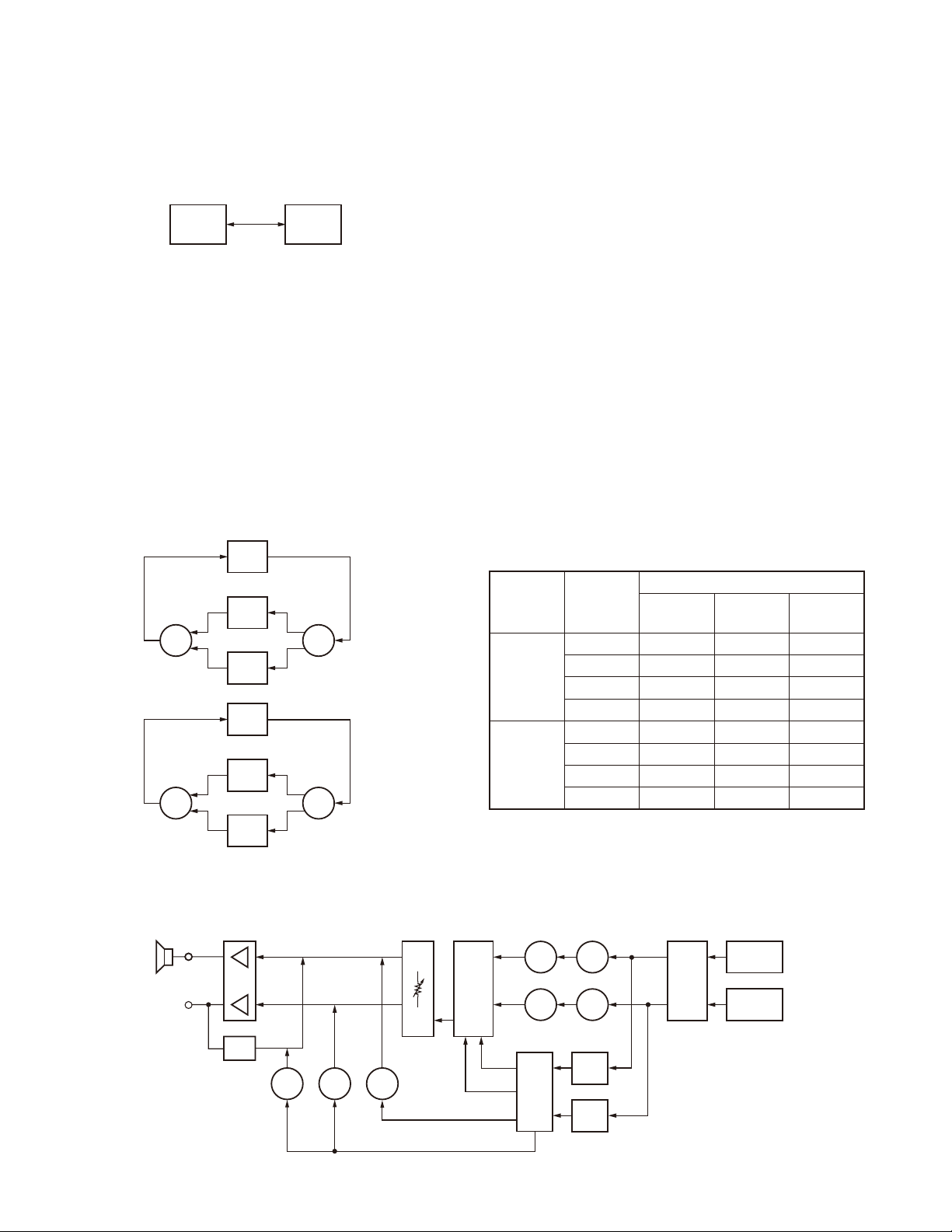
5-4. Narrow/ Wide Switching Circuit
On band A, the receiver bandwidth can be switched
between narrow and wide by selecting IF ceramic filters
CF487 (Narrow) and CF486 (Wide) with a switching circuit
(Q486, Q487, D486, D487).
On band B, the receiver bandwidth can also be switched
between narrow and wide by selecting IF ceramic filter
CF547 (Narrow) and CF546 (Wide) with a switching circuit
(Q546, Q548, D546, D547).
The transmitter deviation can be switched between
narrow and wide by setting the electronic variable resistor
(IC804) on the deviation adjustment point. It is controlled
from the MPU (IC918).
IC486
FM IC
CF WIDE
CF486
D486
D546
CF NARROW
CF487
IC546
FM IC
CF WIDE
CF546
CF NARROW
CF547
D487
D547
6. AF Signal System
6-1. Beep Circuit and Mute Circuit
A beep sound is generated by the MPU (IC918) and goes
to cross point switch (IC806). This signal is switched by
the cross point switch and is input to the electronic volume
(IC804). While the beep signal is output from the MPU,
audio signals for each band are muted by the cross point
switch with the serial data from the MPU (IC918). The beep
signal that has had its level adjusted by an electronic volume
is input to AF amplifi er (IC801).
6-2. Speaker Switching Circuit
There are two speaker jacks, J801 (SP1) and J802 (SP2).
The AF signals can be output in various combinations
matching the internal speakers. When an external speaker is
not connected to J802 (SP2), the J802 signal is added to the
AF amplifi er input of SP1 via the ATT circuit, and is output
through J801 (SP1). When an external speaker is connected
to J802 (SP2), it is output separately from a speaker for A /
B band. Crossing point switch connection can be switched
by switching the menu between MODE 1 and 2, and the
connection of SP1 and SP2.
The AF signal output combinations are shown in the
table below.
Mode
MODE 1
MODE 2
Speaker
Setup
None A, B – –
SP1 only x A, B –
SP2 only A – B
SP1, SP2 x A B
None A, B – –
SP1 only x A, B –
SP2 only B – A
SP1, SP2 x B A
Internal
Speaker
Table 1 AF signal output combinations
Band Output
External
SP1
External
SP2
Fig. 10 Narrow/ Wide switching circuit
J801
(SP1)
J802
(SP2)
8
IC801
AF AMP
ATT
Q816
Q804 Q803
Fig. 11 Beep circuit and mute circuit
IC804
E VR
IC806
Cross
Point
SW
MUTE1
MUTE2
BEEP
DTMF
DE-EMPHASIS A
Q806
Q807 Q811
DE-EMPHASIS B
IC918
MPU
Q810
IC805
1/2
IC805
1/2
CTCSS Filter AMP
IC666
Multi
SW
IC486
FM IC (A)
IC546
FM IC (B)
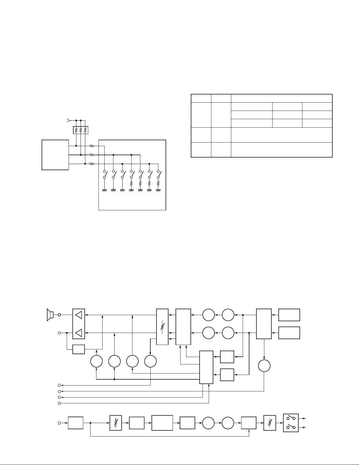
CIRCUIT DESCRIPTION
TM-V71A/V71E
6-3. Microphone Key Input
When the MC-59 (Supplied microphone) is used
■
The pulse is output from the CM terminal of the MPU to
the microphone. The MPU judges which key was pressed
from the number of pulses returned from the microphone.
When the MC-45 (Optional microphone) is used
■
The microphone UP/DOWN and function keys are
connected to the microprocessor analog input. The voltage
when a key is ON operates the corresponding function.
5M
CP952
UP
MIC
CALL
DOWN
22K
100K
VFO
MR
22K
100K
PF
MIC PTT
MIC UP
MIC DW
MPU
IC918
R983
R984
R985
PTT
Fig. 12 Microphone (MC-45) key input
7. Data Terminal and Peripheral Circuits
J607 (Data terminal) is the data communications terminal
on the rear of the transceiver. It handles transmission
control, data input/ output, and squelch signals.
There are two data communications modes: 9600bps
mode and 1200bps mode. 9600bps mode communications
are GMSK and G3RUH packet communications. Unlike with
1200bps AFSK, with this type of high-speed modulation,
frequency modulation is carried out after the digital base
band signals (rectangular wave) are passed through a band
IC804
E VR
Q606Q816 Q804 Q803
IC806
Cross
Point SW
PR1
PR9
SQC
PKS
PKD
J801
(SP1)
J802
(SP2)
IC801
AF AMP
ATT
D607
D609
Limiter
1200bps
9600bps
IC804
E VR
IC805
1/2
limiting filter. For 9600bps GMSK for example, compared
to 4800Hz signals (nearly sine wave signals passed
through a fi lter), the signals have a hissing sound like digital
modulation when listened to by ear. Different types of
modulation, such as GMSK and G3RUH, are distinguished
by the type of band limiting fi lter used.
Pin No.
Pin name
1 PKD
4 PR9
5 PR1
Specifi cation
bps switching 1200bps 9600bps
Modulation input 40mVp-p 2Vp-p
Frequency shift 3±0.5kHz 2.2±0.5kHz
Output level 500mVp-p/10k
Always output during reception
Output level 500mVp-p/10k
Not output when squelch off
Table 2 DATA terminal input/ output level
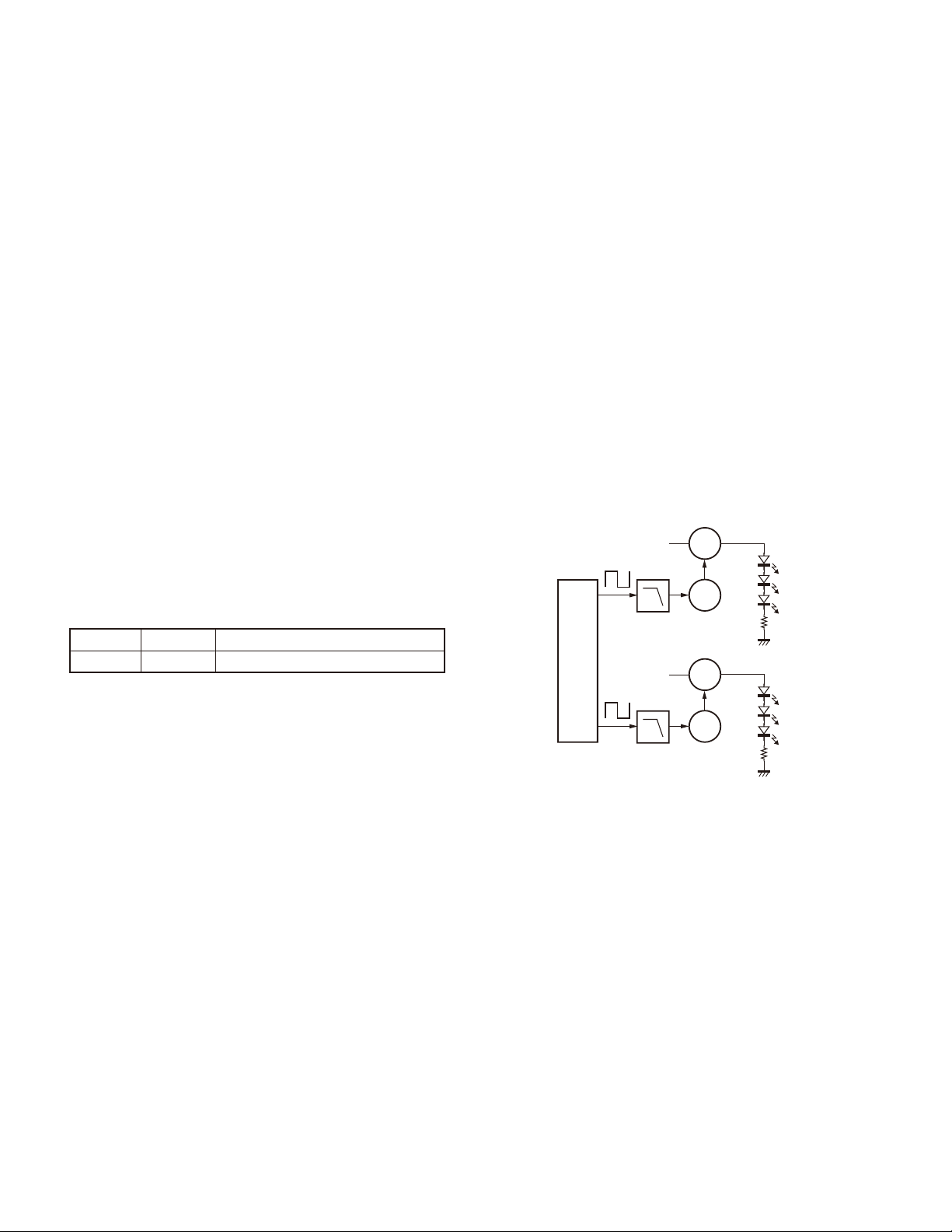
7-1. Transmission Signals
Transmission modulation signals enter from PKD of the
data terminals (J607). The path to the modulation depends
on whether communications are set for 1200bps or 9600bps
mode.
For 1200bps mode, the transmission modulation signals
pass through the analog switch (IC803), and are input to
IC801 (Pin 6). The signals pass through the pre-emphasis
(Q801, Q802), are adjusted by the electronic volume, and
are input to the VCO.
For 9600bps mode, the transmission modulation signals
pass through IC803 and are amplified by the tone amp
(IC802). Signals are then adjusted by the electronic volume,
and are input to the VCO.
The frequency shift depends on the input signal level, so
there is an amplitude limiting circuit (D702, D703) to hold
the signal below 4 Vp-p to avoid extreme shifts. This circuit
ensures that the PKD signal does not go above 4 Vp-p and
there is no extreme frequency shift fl uctuation.
DE-EMPHASIS A
IC486
FM IC (A)
IC546
FM IC (B)
IC807
IC806
Cross
Point
SW
MUTE1
MUTE2
IC803
1/2
BEEP
DTMF
Q806 Q810
Q807
DE-EMPHASIS B
IC918
MPU
PRE-EMPHASIS
Q805 Q808
Q811
IC805
1/2
IC805
1/2
CTCSS Filter AMP
MOD AMP
IC803
2/2
IC666
Multi
SW
Q607
IC804
E VR
Ω
Ω
VCO
TCXO
Fig. 13 Transmission signals
9
TM-V71A/V71E
CIRCUIT DESCRIPTION
7-2. Reception Signals
PR9 is the 9600bps data communications reception
output. It sends the FM detection circuit output (RD signals)
through a buffer amplifi er (Q607). These signals are always
output whether the squelch is open or closed.
PR1 is the 1200bps data communications reception
output. It sends the FM detection circuit output (RA signals)
through a buffer amplifi er (Q606). Output is controlled with
the cross point switch (IC806) according to whether squelch
is open or closed.
PR1: The audio signal that was de-emphasised is switched
by the cross point switch and passed through the
electronic volume. The signal is then buffered by Q606
and is sent to the data output terminal. The PR1 signal
is output when squelch is open.
PR9: The signal switched through IC666 is buffered by
Q607 and is sent to the data output terminal.
7-3. Squelch Signal Output Circuit
The squelch circuits is input to the TNC to prevent
conflicts from occurring between simultaneous
receive mode and transmit mode traffic during packet
communications (only during 1200bps). The SQC signal is
output by the MPU (IC918).
The SQC output can be set to the following using the
menu mode.
An initial value is Busy.TX. The logic of the output is Hi
active. The logic of the output can change by MCP-2A.
Menu No. Display SQC output type
520 SQC.SRC OFF/BUSY/SQL/TX/BUSY.TX/SQL.TX
Table 3 SQC output setting
8. Panel Section
The panel section controls serial communications with
the main unit control section, the key input circuit, the
display circuit, and the brightness circuit through the MPU
(IC903).
8-2. Key, Encoder, Volume Input Circuit
Circuits to operate the panel section keys are connected
to each microprocessor port. The POWER key is pulled up
and the other keys are pulled up within the MPU. Encoder
operating circuits are connected to the MPU and the port is
pulled up. The volume (VOL/SQ) divides the power supply
voltage, reads the A/D port of the MPU, and transfers that
data to the main unit.
8-3. Display Circuit
The MPU controls two LCD drivers (IC906, IC907). It
displays it by connecting IC906 (4 common dots and 39
segment dots) and IC907 (4 common dots and 38 segment
dots) with the LCD.
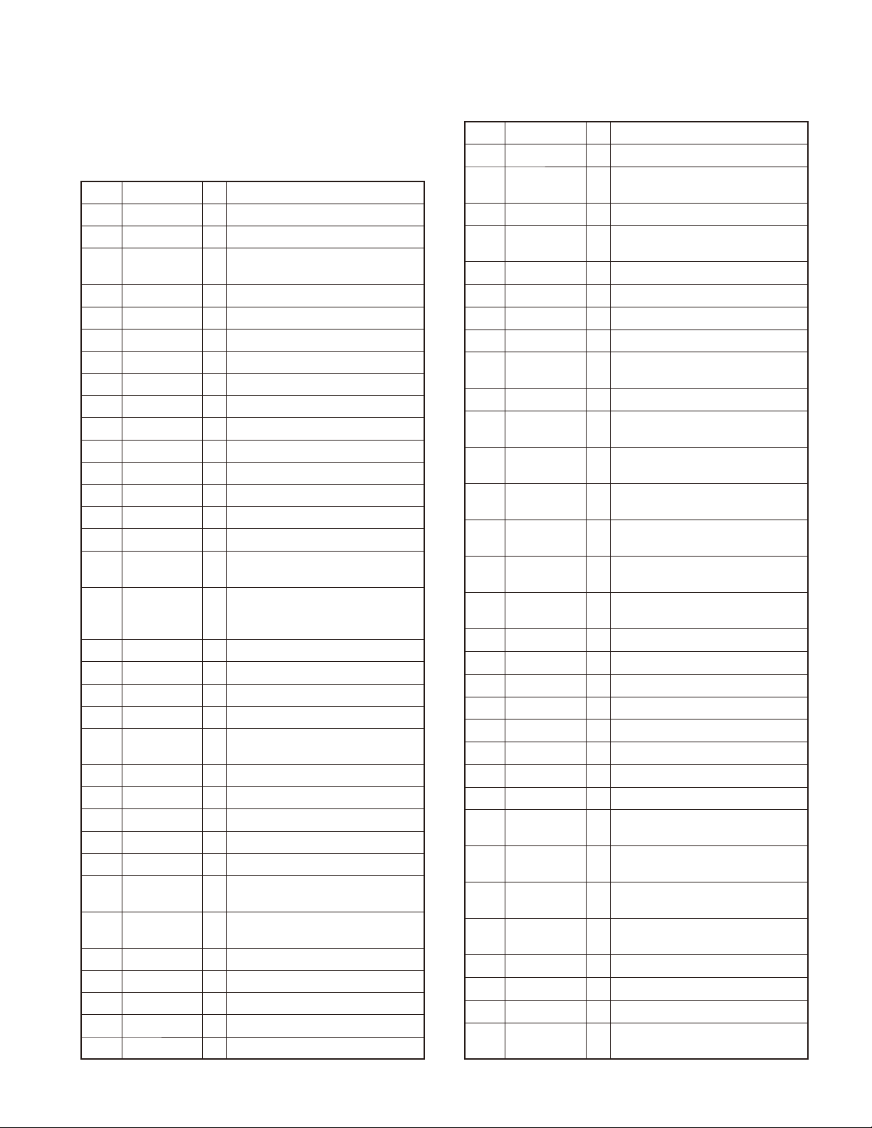
8-4. Brightness Circuit
The illumination color can be set to either amber or
green. The PWM signal output from the MPU passes
through LPF, is converted into the DC voltage, and controls
the current that fl ows to the LED with the transistor. The
duty of the PWM changes the LED brightness to one of
eight levels or OFF.
IC903
MPU
PWM
PWM
10V
LPF
10V
LPF
SW
Q904
Q902
Current
control
SW
Q905
Q903
Current
control
AMBER
GREEN
Fig. 14 Brightness circuit
8-1. Serial Communications Circuit
A buffer IC (IC901, IC902) is used in order to protect the
MPU ports.
10
SEMICONDUCTOR DATA
TM-V71A/V71E
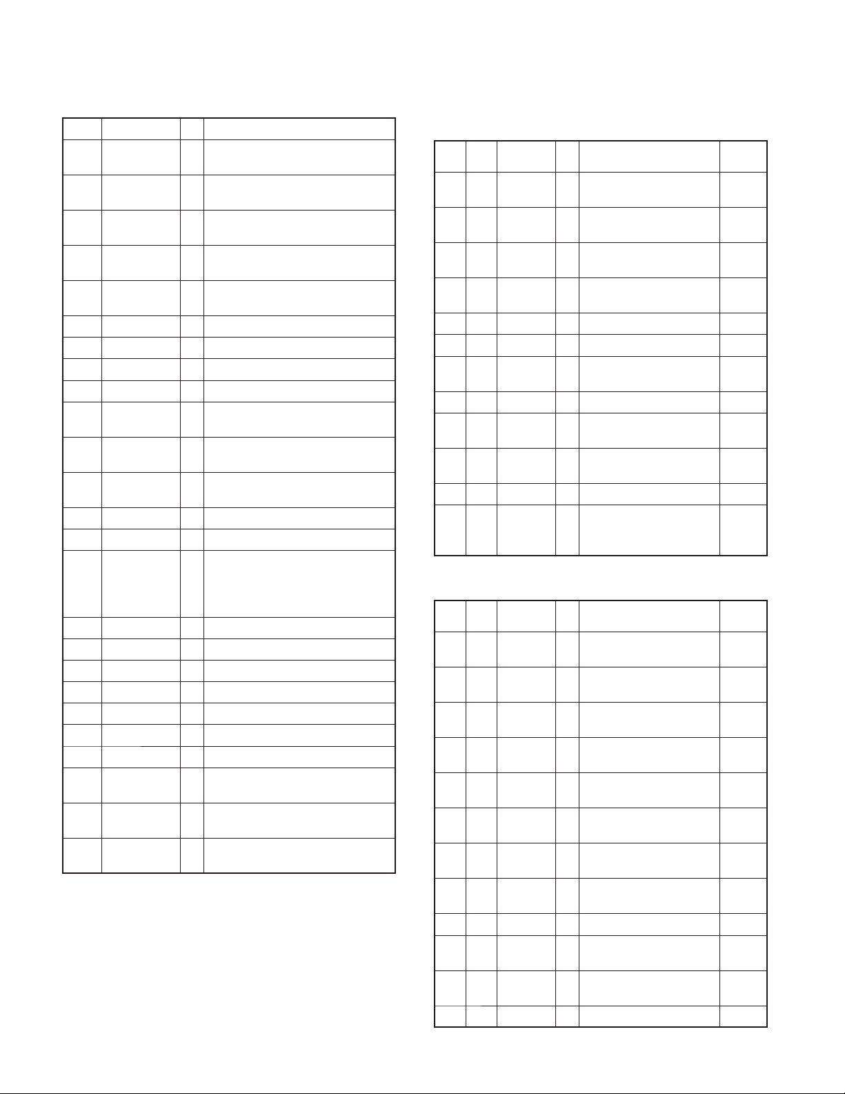
Main MPU: 3062LFGPUKBVB: K
3062LFGPUKBWB: E,M4
(TX-RX (Control) unit (D/6) IC918)
Pin No.
31,32 NC - Not used (GND)
Port Name I/O Function
1 DTMF/1750 O DTMF/Side tone output (D/A)
2 TONE O CTCSS, DCS output (D/A)
3 AMP_STB O
4 BSHIFT O Beat shift circuit control L: Normal
5 NC - Not used (GND)
6 BYTE I Not used (GND)
7 NC - Not used (5V)
8,9 NC - Not used (GND)
10 RESET I System reset
11 XOUT O System clock output (11.0592MHz)
12 VSS I GND
13 XIN I System clock input (11.0592MHz)
14 VCC1 I 5V power supply input
15 NMI I Not used (5V)
16 NC - Not used (Connect to RXD (PC))
17 SIS I
18 INT I
19 XSW_LD O Cross point switch LOAD
PKD96_MUTE
20
21 EEPCS O EEPROM chip select signal
22 EEPSO I EEPROM serial data input
23 MIC_MUTE2 O
24 EEPCK O EEPROM serial clock output
25 EEPSI O EEPROM serial data output
26 BEEP O Beep sound output
27 RXD (PNL) I UART data input from Panel
28 TXD (PNL) O UART data output to Panel
29 TR_DT O
30 TR_CLK O
33 TXD (PC) O UART data output to PC terminal
34 RXD (PC) I UART data input from PC terminal
35 PTT I [PTT] key input
36 PKS (PNL) I Internal TNC PKS input
AF power amplifi er standby switch
L: Standby
Start-up interruption from panel MPU
(Connect to RXD (PNL))
Power supply voltage fall detection
interrupt
( It is detected by approximately 8.8V.)
O PKD 9600bps mute switch H: Mute
MIC mute (After passing the splatter
fi lter.) H: Mute
Data terminal (Serial-parallel, DAC,
PLL, and VGS) for TX-RX unit
CLK terminal (Serial-parallel, DAC,
PLL, and VGS) for TX-RX unit
Pin No.
46~52 SIM6~SIM0 I Type 6~Type 0
73,74 NC - Not used (5V)
Port Name I/O Function
37 SQC (PNL) O Internal TNC SQC output
38 CNT_DT O
39 NC - Not used (GND)
40 CNT_CLK O
41
TCXO_B_MUTE
42
TCXO_A_MUTE
43 DA1_EN O Enable output for DAC (M62364)
44 NC - Not used (5V)
45 MIC_MUTE1 O
53 B_PLLUL I
54 A_PLLEN O
55 A_PLLUL I
56 B_PLLEN O
57 2099_EN O
58 DA2_EN O
59 NC - Not used (GND)
60 VCC2 I 5V power supply input
61 NC - Not used (GND)
62 VSS2 I GND
63 VRST O VGS-1 RESET signal output
64 VEN O VGS-1 ENABLE signal output
65 VPLY I VGS-1 PLAY signal input
66 VBSY I VGS-1 BUSY signal input
67 VSF I
68 TEMP I Temperature protection A/D input
69 PKS (EXT) I
70 SQC (EXT) O
71 CTS (PC) I PTT control terminal from PC terminal
72 RTS (PC) O BUSY control terminal to PC terminal
75 SB_C O
Serial data for DAC (M62364) and
cross point switch
Clock for DAC (M62364) and cross
point switch
O B band TCXO mute switch L: Mute
O A band TCXO mute switch L: Mute
MIC mute (Front of MIC amplifi er)
H: Mute
Unlock detection for B band
H: Lock
PLL enable output for A band
H: Enable
Unlock detection for A band
H: Lock
PLL enable output for B band
H: Enable
Enable output for serial-parallel
conversion IC (BU2099FV)
Enable output for external DAC
(BH2228FV)
Transmission protection A/D input
(FWD side)
PTT control terminal from mini DIN
terminal (PKS)
BUSY control terminal to mini DIN
terminal (SQC)
Main power switch of transceiver
(SBSW)
11
TM-V71A/V71E
SEMICONDUCTOR DATA
Pin No.
Port Name I/O Function
76 PKD_SEL O
77 VU_TX O
78 CM I
79 MIC_DW I
80 MIC_UP I
81 SQ_B I Noise level A/D input for B band
82 SQ_A I Noise level A/D input for A band
83 SM_B I S-meter level A/D input for B Band
84 SM_A I S-meter level A/D input for A Band
85 TOIN_B I
86 TOIN_A I
87 SCB_C O
88 S5M_C O Power switch for RS-232C driver
89 BATT - Not used
90 DTMFPD O
91 DTMFDT I DTMF serial data input
92 DTMFCLK O DTMF clock
93 DTMFDET I DTMF data detection terminal
94 AVSS I GND
95 AF_CAL I Not used
96 VREF I Reference voltage
97 AVCC I Analog power supply
98 AF_MUTE2 O
99 AF MUTE1 O
100 AMP_MUTE O
PKD input switching (PKD (PNL) or
PKD (EXT))
L:VHF TX, H:UHF TX (V/U switching)
H: Mute
MIC key serial input terminal
(for MC-59)
MIC key (DOWN, MR, PF) input
(for MC-45)
MIC key (UP, CALL, VFO) input
(for MC-45)
B band (CTCSS, DCS, and WX)
decoder A/D input
A band (CTCSS, DCS, and WX)
decoder A/D input
+B power switch for control unit
(power supply for AF power amplifi er)
Power down mode control terminal
of the DTMF IC (Reset processing
when the turning the transceiver
power ON.)
AF mute 2 (Front of AF power amplifi er) L: Mute
AF mute 1 (Front of AF power amplifi er) L: Mute
AF power amplifi er mute switch
H: Mute
Shift Register: BU2099FV (TX-RX unit (A/6) IC576)
Pin
Port
No.
6 Q0 WN_A O
7Q1
8 Q2 8TVA_C O
9 Q3 5RUA_C O
10 Q4 VHF_AIP O AIP switch (A band/B band) H
11 Q5 FAN_C O FAN control switch H
12 Q6 SFT_A O VCO switching (A band)
13 Q7 UHF_AIP O AIP switch (A band/B band) H
14 Q8 8TUA_C O
15 Q9 5RVA_C O
16 Q10
17 Q11 5RAM_C O
Pin name I/O Function
name
Wide/Narrow switching
SW for A band
VU_SEL_A
BP_SFT_A
O VCO VHF/UHF select
8V power supply control
switch for A Band VHF TX
5V power supply switch
for A Band UHF BPF
8V power supply control
switch for A band UHF TX
5V power supply switch
for A band VHF BPF
O
BPF shift switch for A band
5V power supply switch
(DET A switching SW) for
A band AM
Active
level
H (Narrow)
/ L (Wide)
H: VHF
L: UHF
H
H
H: Shift ON
L: Shift OFF
H
H
H
H (DET A)
/ L (AM)
Shift Register: BU2099FV (TX-RX unit (A/6) IC577)
Pin
Port
No.
6 Q0 WN_B O
7Q1
8 Q2 8TUB_C O
9 Q3 5RUB_C O
10 Q4 PR9_SEL O PR9 output switching SW
11 Q5
12 Q6 SFT_B O VCO switching (B band)
13 Q7 8TVB_C O
14 Q8 NC - Not used (5V) H
15 Q9 5RVB_C O
16 Q10 5R8B_C O
17 Q11
Pin name I/O Function
name
Wide/Narrow switching
SW for B band
VU_SEL_B
PR (PNL)_SEL
BP_SFT_B
O VCO VHF/UHF select
8V power supply control
switch for B band UHF TX
5V power supply switch
for B band UHF BPF
DET output switching SW
O
to internal TNC
8V power supply control
switch for B band VHF TX
5V power supply switch
for B band VHF BPF
5V power supply switch
for B band 800MHz BPF
O
BPF shift switch for B band
Active
level
H (Narrow)
/ L (Wide
)
H: VHF
L: UHF
H
H
H (DET_A)
/ L (DET_B)
H (DET_A)
/ L (DET_B
H: Shift ON
L: Shift OFF
H
H
H
H
12
SEMICONDUCTOR DATA
TM-V71A/V71E
Electorical Volume IC: M62364FP-F (TX-RX (Control) unit (D/6) IC804)
Pin No.
Pin name
1 VIN1 B band balance adjustment input
2 VOUT1 B band balance adjustment output
3 VOUT2 A band blance adjustment output
4 VIN2 A band blance adjustment input
9 VIN3 TX deviation adjustment input
10 VOUT3 TX deviation adjustment output
11 VOUT4 MIC sensitivity adjustment output
12 VIN4 MIC sensitivity adjustment input
13 VIN5 SP2 output VOL adjustment input
14 VOUT5 SP2 output VOL adjustment output
15 VOUT6 SP1 output VOL adjustment output
16 VIN6 SP1 output VOL adjustment input
21 VIN7
22 VOUT7
23 VOUT8
24 VIN8 DATA terminal PKD input level adjustment input
DATA terminal PR1 output level adjustment input
DATA terminal PR1 output level adjustment output
DATA terminal PKD input level adjustment output
Function
Cross Point Switch: BU8241FS (TX-RX (Control) unit (D/6) IC806)
Pin No.
Pin name
5 IN1
6 IN2
7 IN3
8 IN4 Beep signal input from MPU
9 IN5 MIC audio input (MIC amplifi er and AGC output)
10 IN6
11 IN7 RX audio input to internal TNC
12 IN8 VGS-1 playing audio input
13 OUT8 SP2 audio output VOL
14 OUT7 SP1 audio output VOL
15 OUT6
16 OUT5 VGS-1 recording audio output
17 OUT4 Audio level detection output to MPU
18 OUT3 RX audio output to DTMF IC
19 OUT2
20 OUT1 RX audio output to internal TNC
A band RX audio input (De-emphasis circuit output)
B band RX audio input (De-emphasis circuit output)
DTMF (1750Hz tone) encode signal input from MPU
PKD 1200bps data input and Audio input from PC
DATA terminal PR1 output
(Input to DAC for level adjustment)
MIC audio output
(Limiter and Pre-emphasis circuit input)
Function
Panel MPU: 3062LFGPUKBZA (Display unit IC903)
Pin No. Port Name I/O Function
1 KEY4 I [CALL] key input
2 KEY3 I [MHz] key input
3 NC - Not used (5V)
4 KEY2 I [MR] key input
5 KEY1 I [VFO] key input
6 BYTE I Not used (GND)
7 NC - Not used (GND)
8 ENC_B I Encoder 1
9 NC - Not used (GND)
10 RESET I System reset
11 XOUT O System clock output (11.0592MHz)
12 VSS I GND
13 XIN I System clock input (11.0592MHz)
14 VCC I 5V power supply input
15 NMI I Not used (5V)
16 ENC_A I Encoder 2 (INT)
17 RXD_INT I RXD detection
18 POWER I Power switch detection interrupt
19,20 NC - Not used (GND)
21 LCD_CE_1 O LCD driver 1 CE
22 LCD_CLK_1 O LCD driver 1 CLK
23 LCD_DT_1 O LCD driver_1 data
24 AMBER O Dimmer output PWM (Amber)
25 NC - Not used (GND)
26 GREEN O Dimmer output PWM (Green)
27 PSW O 5V switch L: ON
28 NC - Not used (GND)
29 TXD O UART output to main MPU
30 RXD I UART input from main MPU
31 CLK - Not used (GND)
32 BUSY - Not used (5V)
33~38 NC - Not used (GND)
39 EMP - Not used (GND)
40~43 NC - Not used (GND)
44 CE - Not used (5V)
45~59 NC - Not used (GND)
60 VCC I 5V power supply input
61 NC - Not used (GND)
62 VSS I GND
13
TM-V71A/V71E
SEMICONDUCTOR DATA
Pin No. Port Name I/O Function
63~67 NC - Not used (GND)
68 LCD_DT_2 O LCD driver 2 data
69 LCD_CLK_2 O LCD driver 2 CLK
70 LCD_CE_2 O LCD driver 2 CE
71 NC - Not used (5V)
72 KEY13 I [PM] key input
73 KEY12 I [Band SEL B] key input
74 KEY11 I [Band SEL A] key input
75 KEY10 I [PF2] key input
76 KEY9 I [PF1] key input
77 KEY8 I [LOW] key input
78 KEY7 I [REV] key input
Pin No. Port Name I/O Function
79~90 NC - Not used (GND)
91 VOL_B I AF VOL (Band B) A/D input
92 VOL_A I AF VOL (Band A) A/D input
93 SQL_B I SQL (Band B) A/D input
94 AVSS I GND
95 SQL_A I SQL (Band A) A/D input
96 VREF I Reference voltage input
97 AVCC I Analog power supply input
98 NC - Not used (5V)
99 KEY6 I [TONE] key input
100 KEY5 I [F] key input
COMPONENTS DESCRIPTION
DISPLAY UNIT (X54-3590-00)
Ref. No. Use / Function
IC901 Buffer RXD
IC902 Buffer TXD
IC903 MPU
IC904 5V AVR 5V
IC905 Reset IC for MPU
IC906,907
Q901 Switching SW5V for LCD driver IC
Q902 Switching GR10V control
Q903 Switching AM10V control
Q904 Switching 10V for Green LED
Q905 Switching 10V for Amber LED
D901~921
D922~951
D952~983
D984~986
D987 LED Green
D988,989
LCD driver
Switching Protection from surge input
LED Amber
LED Green
LED Amber
Varistor Protection from surge input
Operation / Condition / Compatibility
TX-RX UNIT (X57-731X-XX)
Ref. No. Use / Function
IC1 PLL IC A band
IC66 PLL IC B band
IC131 Power module VHF
IC161 Power module UHF
IC186
IC187 OP amplifi er for APC
IC486 FM IC A band
IC487 OP amplifi er AGC amplifi er
IC546 FM IC B band
IC576 Shift register
2CH analog
switch
Operation / Condition / Compatibility
APC voltage VHF/UHF select
Q0: Wide/Narrow select for A band
Q1: VU_Select for A band
Q2: 8TVA control
Q3: 5RUA control
Q4: VHF AIP control
Q5: FAN control
Q6: VCO shift for A band
Q7: UHF AIP control
Q8: 8TUA control
Q9: 5RVA control
Q10: VHF BPF control for A band
Q11: 5RAM control
14
TM-V71A/V71E
COMPONENTS DESCRIPTION
Ref. No. Use / Function
IC577 Shift register
IC578 8V AVR 8C
IC579 5V AVR 5C
IC606
IC666
IC667 D/A
IC668 Amplifi er LNA for 1.2G RX
IC801 Audio amplifi er
IC802 OP amplifi er MIC amplifi er/ALC
IC803 OP amplifi er Pre-emphasis/Modulation
IC804
IC805
IC806
IC807
IC916 EEPROM
IC917 Multiplexer PKD line select
IC918 MPU
IC919 Reset IC Backup signal
IC920 Reset IC Reset signal for MPU
IC921 DTMF decoder
IC951 Buffer Panel output line
IC952 10V AVR PB
IC953 5V AVR 5C
Q1 Ripple fi lter for A band charge pump
Q2,3 Switching A band charge pump
Q4 Ripple fi lter for A band VCO
Q5 Amplifi er to f-in on PLL IC
Q6 Switching
RS-232C driver IC
4CH multiplexer
Electorical
volume IC
4CH OP amplifi er
Cross point
switch IC
2CH analog
switch
Operation / Condition / Compatibility
Q0: Wide/Narrow select for B band
Q1: VU_Select for B band
Q2: 8TUB control
Q3: 5RUB control
Q4: PR9 select
Q5: PR for panel select
Q6: VCO shift for B band
Q7: 8TVB control
Q8: Not used
Q9: 5RVB control
Q10: 5R8B cintrol
Q11: VHF BPF control for B band
RS-232C driver
Detect signal line select
Ao1: Forward Ref
Ao2: Reverse Ref
Ao3: BPF control for B band
Ao4: BPF control for B band
Ao5:
TCXO reference voltage for B band
Ao6:
TCXO reference voltage for A band
Modulation line select
AV reference voltage/PKD amplifi er/
LSD amplifi er A/LSD amplifi er B
Audio line select
Modulation line for TCXO select
VHF/UHF selection for A band VCO
(On when A band VHF is selected)
Ref. No. Use / Function
Q7 Amplifi er Local amplifi er for A band
Q8 Switching
Q9 Switching
Q66 Ripple fi lter for B band charge pump
Q67,68 Switching B band charge pump
Q69 Ripple fi lter for A band VCO
Q70 Amplifi er to f-in on PLL IC
Q71 Switching
Q72 Amplifi er Local amplifi er for B band
Q73 Switching
Q74 Switching
Q131 Amplifi er VHF TX drive amplifi er
Q132 Switching
Q161 Amplifi er UHF TX Pre-drive amplifi er
Q162 Amplifi er UHF TX drive amplifi er
Q163 Switching
Q186 Switching
Q226 Mixer A band VHF RX
Q227 Amplifi er A band VHF RX 2nd LNA
Q228 Amplifi er A band VHF RX LNA
Q229 Switching
Q291 Mixer B band VHF RX
Q292 Amplifi er B band VHF RX 2nd LNA
Q293 Amplifi er B band VHF RX LNA
Q294 Switching
Q361 Mixer A band UHF RX
Q362 Amplifi er A band UHF RX 2nd LNA
Q363 Amplifi er A band UHF RX LNA
Q400 Switching
Q406 Mixer B band UHF RX
Q407 Amplifi er B band UHF RX 2nd LNA
Q408 Amplifi er B band UHF RX LNA
Q450 Switching
Q456 Amplifi er Local amplifi er for 1.2G RX
Q457 Mixer B band 1.2G RX
Q459 Amplifi er B band 1.2G RX LNA
Operation / Condition / Compatibility
A band PLL f-in fi lter select
(On when B band VHF is selected)
B band f-in VHF fi lter frequency shift
VHF/UHF selection for B band VCO
(On when A band VHF is selected)
B band PLL f-in fi lter select
(On when B band VHF is selected)
A band f-in VHF fi lter frequency shift
Mute Vgg line for VHF power module
Mute Vgg line for UHF power module
VHF/UHF selection (On when VHF TX)
Q228 gain drop (VHF AIP function)
(On when VHF AIP ON)
Q293 gain drop (VHF AIP function)
(On when VHF AIP ON)
Q363 gain drop (UHF AIP function)
(On when UHF AIP ON)
Q408 gain drop (UHF AIP function)
(On when UHF AIP ON)
15
TM-V71A/V71E
COMPONENTS DESCRIPTION
Ref. No. Use / Function
Q486 Switching
Q487 Switching
Q488 Switching
Q489 Amplifi er AM IF AGC amplifi er
Q490 Switching AGC switch
Q491 Amplifi er AM IF AGC amplifi er
Q492 Switching AGC switch
Q493 Amplifi er
Q494 Amplifi er AM IF AGC amplifi er
Q495 Amplifi er A band 1st IF amplifi er
Q496 Switching
Q546 Switching
Q547 Tripler 16.8MHz×3
Q548 Switching
Q549 Switching
Q550 Switching
Q551 Amplifi er B band 1st IF amplifi er
Q572 Switching Make BP_SFT_B signal
Q573 Switching Make BP_SFT_B_I signal
Q574 Switching Make BP_SFT_A signal
Q575 Switching Make BP_SFT_A_I signal
Q576 Switching Fan control (On when Fan turn)
Q578 Switching
Q579 Switching
Q580 Switching
Q582 Switching
Q583 Switching
Q584 Switching
Q585 Switching 8TV switch (On when VHF TX)
Q586 Switching 8TU switch (On when UHF TX)
Q587 Switching
Operation / Condition / Compatibility
Ceramic fi lter select (On when FMNarrow is selected on A band)
Ceramic fi lter select (On when FMWide is selected on A band)
Squelch select (On when FMNarrow is selected on A band)
A band discriminator dump switch (On
when FM-Wide is selected on A band)
AGC voltage select (AM/FM) (On
when FM is selected on A band)
Ceramic fi lter select (On when FMNarrow is selected on B band)
Ceramic fi lter select (On when FMWide is selected on B band)
Squelch select (On when FMNarrow is selected on B band)
B band discriminator dump switch (On
when FM-Wide is selected on B band)
5RVA switch
(On when A band VHF is selected)
5RUA switch
(On when A band UHF is selected)
5RAM switch
(On when A band AM is selected)
5RVB switch
(On when B band VHF is selected)
5RUB switch
(On when B band UHF is selected)
5R8B switch (On when B band 1.2G
is selected)
8TVA switch (On when A band VHF TX)
Ref. No. Use / Function
Q588 Switching
Q589 Switching
Q590 Switching
Q591,592
Q606 Amplifi er
Q607 Amplifi er
Q641 Switching FAN control switch
Q642 Switching IGN control switch
Q644 Amplifi er VHF TX Pre-drive
Q701,702
Q703,704
Q705 Oscilator VHF VCO
Q706 Oscilator UHF VCO
Q707 Amplifi er RF amplifi er
Q751,752
Q753,754
Q755 Oscilator VHF VCO
Q756 Oscilator UHF VCO
Q757 Amplifi er RF amplifi er
Q801 Amplifi er AGC control
Q802 Switching Audio amplifi er (IC801) mute switch
Q803,804
Q805 Active fi lter for splatter fi lter
Q806 Active fi lter A band de-emphasis fi lter amplifi er
Q807 Active fi lter B band de-emphasis fi lter amplifi er
Q808 Active fi lter for splatter fi lter
Q809 Switching MIC mute
Q810 Active fi lter A band de-emphasis fi lter amplifi er
Q811 Active fi lter B band de-emphasis fi lter amplifi er
Q812 Switching PKD 9600bps mute switch
Q816 Switching Audio line mute switch
Q817 Switching
Q916,917
Q918 Switching Over voltage protection switch
Q951 Switching SCB switch
Q952 Switching S5M switch
Q953 Switching SCB switch
Q954 Switching S5M switch
Q955 Switching PR1 amplifi er for Panel
Switching
Switching Shift VCO frequency range
Switching VCO select (VHF/UHF)
Switching Shift VCO frequency range
Switching VCO select (VHF/UHF)
Switching Audio line mute switch
Switching
Operation / Condition / Compatibility
8TUA switch (On when A band UHF TX)
8TVB switch (On when B band VHF TX)
8TUB switch (On when B band UHF TX)
SB switch
(On during transceiver power ON)
PR1 amplifi er in DATA terminal (J607)
PR9 amplifi er in DATA terminal (J607)
TCXO modulation level change
(On when UHF TX)
Crystal oscillator frequency shift switch
16
TM-V71A/V71E
COMPONENTS DESCRIPTION
Ref. No. Use / Function
D1
D2 Voltage shift A band charge pump
D3,4 Switching Speed up switch for ripple fi lter
D5,6 Switching Speed up switch for Loop fi lter
D10~13 Switching VHF/UHF BPF select
D14,18 Switching
D15 Switching RF switch (On when A band UHF)
D16 Switching
D17 Switching
D19 Switching
D20,21 Switching VHF BPF shift
D22 Switching
D23 Switching RF switch (On when B band UHF)
D24 Switching
D25 Switching
D26 Switching
D27 Switching
D28 Switching
D29 Switching
D30~33 Switching VHF/UHF BPF select
D34,35 Switching VHF BPF shift
D66 Switching B band PLL unlock signal
D67 Voltage shift B band charge pump
D68,69 Switching Speed up switch for ripple fi lter
D70,71 Switching Speed up switch for Loop fi lter
D130 Switching
D131 Switching
D132
D133
D134,135
D136
D160 Switching
D161 Switching
D162
D163
D164,165
D166
Reverse current
prevention
Temperature
compensation
5.1V Zener diode
Switching VHF TX RF switch
Temperature
compensation
Temperature
compensation
5.1V Zener diode
Switching UHF TX RF switch
Temperature
compensation
Operation / Condition / Compatibility
A band PLL unlock signal
RF switch (On when A band VHF TX)
RF switch (On when A band VHF RX)
RF switch (On when A band UHF RX)
RF switch (On when A band UHF TX)
RF switch (On when B band VHF TX)
RF switch (On when B band VHF RX)
RF switch (On when B band UHF RX)
RF switch (On when B band VHF TX)
RF switch (On when B band UHF TX)
Line mute (On when B band UHF TX)
Line mute (On when A band UHF TX)
RF switch (On when A band VHF TX)
RF switch (On when B band VHF TX)
for VHF drive circuit
Over voltage prevention
for thermal protection circuit
RF switch (On when A band UHF TX)
RF switch (On when B band UHF TX)
for UHF drive circuit
Over voltage prevention
for thermal protection circuit
Ref. No. Use / Function
D186 Switching RF switch
D187 Switching RF switch
D188 Switching RF switch
D189 Switching RF switch
D190
D191 Rectifi cation Forward voltage for APC circuit
D192 Rectifi cation Reverse voltage for APC circuit
D193
D226 Switching
D227 Switching
D229 Switching BPF frequency shift
D230,231
D232 Switching BPF frequency shift
D233,234
D238 Switching BPF frequency shift
D239,240
D241 Switching BPF frequency shift
D242,243
D291 Switching
D292 Switching
D294 Switching BPF frequency shift
D295,296
D297 Switching BPF frequency shift
D298,299
D303 Switching BPF frequency shift
D304,305
D306 Switching BPF frequency shift
D307,308
D356 Switching RF mute
D357,358
D361 Switching
D362,363
D364,365
D367,368
D370,371
D375,376
D377~379
D406 Switching IF switch (on when B band UHF RX)
Reverse current
prevention
5.1V Zener diode
Varicap Tune the A band VHF BPF
Varicap Tune the A band VHF BPF
Varicap Tune the A band VHF BPF
Varicap Tune the A band VHF BPF
Varicap Tune the B band VHF BPF
Varicap Tune the B band VHF BPF
Varicap Tune the B band VHF BPF
Varicap Tune the B band VHF BPF
Limiter VHF RF limiter
Switching
Varicap Tune the A band UHF BPF
Varicap Tune the A band UHF BPF
Varicap Tune the A band UHF BPF
Varicap Tune the A band UHF BPF
Varicap Tune the A band UHF BPF
Operation / Condition / Compatibility
APC circuit
Over voltage prevention
IF switch (On when A band VHF RX)
Local signal switch
(On when A band VHF RX)
IF switch (On when B band VHF RX)
Local signal switch
(On when B band VHF RX)
IF switch (On when A band UHF RX)
Local signal switch
(On when A band UHF RX)
17
TM-V71A/V71E
COMPONENTS DESCRIPTION
Ref. No. Use / Function
D407,408
D409,410
D412,413
D415,416
D419~421
D423,424
D451 Switching RF mute
D456 Switching IF switch (on when 1.2G RX)
D457 Switching
D486,487
D488 Detection AM AGC voltage detection
D489 Detection AM detection
D546,547
D576
D578
D580
D582
D583
D584
D606
D607 Limiter Prevention from over level input
D608
Switching
Varicap Tune the B band UHF BPF
Varicap Tune the B band UHF BPF
Varicap Tune the B band UHF BPF
Varicap Tune the B band UHF BPF
Varicap Tune the B band UHF BPF
Switching A band RX ceramic fi lter select
Switching B band RX ceramic fi lter select
Reverse current
prevention
Reverse current
prevention
Reverse current
prevention
Reverse current
prevention
Reverse current
prevention
Reverse current
prevention
Reverse current
prevention
Reverse current
prevention
Operation / Condition / Compatibility
Local signal switch
(on when B band UHF RX)
Local signal switch (on when 1.2G RX)
5RA output
5RB output
5RB output
8TV control for A band
8TV control for B band
8TU control
for alignment
for alignment
Ref. No. Use / Function
D609
D610,611
D612 Surge absorber Protection from surge input
D701 Switching UHF VCO shift
D703 Varicap UHF VCO tune
D704 Varicap VHF VCO tune
D705 Varicap UHF VCO tune
D707 Varicap VHF VCO tune
D708 Switching VHF VCO shift
D709 Varicap for VHF VCO modulation
D710 Varicap for UHF VCO modulation
D751 Switching UHF VCO shift
D753 Varicap UHF VCO tune
D754 Varicap VHF VCO tune
D755 Varicap UHF VCO tune
D757 Varicap VHF VCO tune
D758 Switching VHF VCO shift
D759 Varicap for VHF VCO modulation
D760 Varicap for UHF VCO modulation
D801,802
D916
D951~953
D954
D955
D956 Poly-switch Current limit
D957
Limiter Prevention from over level input
Switching Protection from surge input
Switching MIC mute
18V Zener diode
Limiter Protection from surge input
Reverse current
prevention
5.1V Zener diode
Reverse current
prevention
Operation / Condition / Compatibility
Over voltage prevention
8C
Over voltage prevention
5M
18
TERMINAL FUNCTION
TM-V71A/V71E
DISPLAY UNIT (X54-3590-00)
Pin No.
Name I/O Function
CN902
1 GND - GND
2 SW5V I Switched 5V
3 KEY11 O Volume key signal (A band)
4 VOL_A O AF volume voltage (A band)
5 SQL_A O SQL volume voltage (A band)
CN903
1 GND - GND
2 SW5V O Switched 5V
3 KEY11 I Volume key signal (A band)
4 VOL_A I AF volume voltage (A band)
5 SQL_A I SQL volume voltage (A band)
CN904
1 GND - GND
2 SW5V I Switched 5V
3 KEY12 O Volume key signal (B band)
4 VOL_B O AF volume voltage (B band)
5 SQL_B O SQL volume voltage (B band)
CN905
1 GND - GND
2 SW5V O Switched 5V
3 KEY12 I Volume key signal (B band)
4 VOL_B I AF volume voltage (B band)
5 SQL_B I SQL volume voltage (B band)
CN912 (to TX-RX (CONTROL) unit D/6)
1 PB I 10V for Display unit
2 PB I 10V for Display unit
3 GND - GND
4 GND - GND
5 RXD I Serial signal input (from main MPU)
6 TXD O Serial signal output (to main MPU)
TX-RX UNIT (X57-731X-XX) (A/6): TX-RX Section
Pin No.
Name I/O Function
CN641 (for FAN)
1SB OFAN 1+
2 FAN_C I FAN 1-
CN642 (for VGS-1)
1 VBSY I VGS-1 busy signal
2 VPLY I VGS-1 play signal
Pin No.
15~26 NC - No connection
Name I/O Function
3 SO - No connection
4 DATA O Data signal output for VGS-1
5 CLK O CLK for VGS-1
6 VEN O Enable signal for VGS-1
7 USEL - No connection
8 VRST O VGS-1 reset signal
9 DGND - DGND
10 AGND - GND
11 VAI I VGS-1 audio input
12 VAO O VGS-1 audio output
13 AGND - GND
14 5C O Switched 5V for VGS-1
CN676 (to TX-RX (CONTROL) unit D/6)
1 GND - GND
2CB OB
CN677 (to TX-RX (CONTROL) unit D/6)
1 S5M I Switched 5V for RS-232C driver (IC606)
2 NC - No connection
3 8C O Switched 8V
4 NC - No connection
5 5C O Switched 5V
6 NC - No connection
7 SB_C I SB control signal
8 ILLM O Illumination signal
9 IGN O Ignition signal
10 TXD (PC) I TXD input for PC
11 RXD (PC) O RXD output from PC
12 RTS (PC) I RTS input for PC
13 CTS (PC) O CTS output from PC
14 SQC (EXT) O SQC signal output
15 PKS (EXT) O PKS signal output
16 PKD (EXT) I PKD signal input
17 PR1 (EXT) I PR1 signal input
18 GND - GND
19 SM_A O A band S-meter voltage output
20 SQ_A O A band SQL voltage output
21 VSF O VSF voltage output
22 TEMP O Thermistor voltage output
23 SM_B O B band S-meter voltage output
24 SQ_B O B band SQL voltage output
19
TM-V71A/V71E
TERMINAL FUNCTION
Pin No.
Name I/O Function
25 GND - GND
26 DET_A O A band detect signal output
27 PR (PNL) O PR detect signal output for panel
28 DET_B O B band detect signal output
29 GND - GND
30 VBSY I VGS-1 busy signal
31 VPLY I VGS-1 play signal
32 VEN I Enable signal for VGS-1
33 VRST I VGS-1 reset signal
34 DA2_EN I Enable signal for D/A IC (IC667)
35 2099_EN I Enable signal for shift register (IC576)
36 TR_CLK I Clock
37 TR_DT I Data
38 B_PLLEN I Enable signal for B band PLL (IC66)
39 A_PLLUL O Unlock signal from A band PLL (IC1)
40 A_PLLEN I Enable signal for A band PLL (IC1)
41 B_PLLUL O Unlock signal from B band PLL (IC66)
42 VGSPLAY O Audio output from VGS-1
43 TCXO_A I Modulation signal for A band TCXO
44 VCO_B I Modulation signal for B band VCO
45 VCO_A I Modulation signal for A band VCO
46 TCXO_B I Modulation signal for B band TCXO
47 VGSREC I Audio input (VGS-1)
48 SIM0 O Type
49 SIM1 O Type
50 SIM2 O Type
J606 (8-pin mini DIN: PC terminal)
1 RTS O Request to send
2 CTS I Clear to send
3 TXD O Transmit data
4 GND - GND
5 RXD I Receive data
6 NC - No connection
7 NC - No connection
8 NC - No connection
J607 (6-pin Mini DIN: DATA terminal)
1 PKD I Packet data input
2 GND - GND
3 PKS I Packet standby
4 PR9 O Output of detected 9600bps data
5 PR1 O Output of detected 1200bps data
Pin No.
Name I/O Function
6 SQC O Squelch control output
TX-RX UNIT (X57-731X-XX) (B,E/6): VCO A Section
Pin No.
Name I/O Function
CN701
1 SHIFT I VCO shift signal
2 V/U I VHF VCO/UHF VCO select signal
3 CV I VCO control voltage
4 MOD I Modulation signal input
CN702
1 OUT O Oscillation signal output
2 E - GND
3 8C I 8V for VCO
TX-RX UNIT (X57-731X-XX) (C,F/6): VCO B Section
Pin No.
Name I/O Function
CN751
1 SHIFT I VCO shift signal
2 V/U I VHF VCO/UHF VCO select signal
3 CV I VCO control voltage
4 MOD I Modulation signal input
CN752
1 OUT O Oscillation signal output
2 E - GND
3 8C I 8V for VCO
TX-RX UNIT (X57-731X-XX) (D/6): CONTROL Section
Pin No.
Name I/O Function
CN960 (to TX-RX unit A/6)
1 SIM2 I Type
2 SIM1 I Type
3 SIM0 I Type
4 VGSREC O Audio output (VGS-1)
5 TCXO_B O Modulation signal for B band TCXO
6 VCO_A O Modulation signal for A band VCO
7 VCO_B O Modulation signal for B band VCO
8 TCXO_A O Modulation signal for A band TCXO
9 VGSPLAY I Audio input from VGS-1
10 B_PLLUL I Unlock signal from B band PLL (IC66)
11 A_PLLEN O Enable signal for A band PLL (IC1)
12 A_PLLUL I Unlock signal from A band PLL (IC1)
20
TERMINAL FUNCTION
TM-V71A/V71E
Pin No.
13 B_PLLEN O Enable signal for B band PLL (IC66)
14 TR_DT O Data
15 TR_CLK O Clock
16 2099_EN O Enable signal for shift register (IC576)
17 DA2_EN O Enable signal for D/A IC (IC667)
18 VRST O VGS-1 reset signal
19 VEN O Enable signal for VGS-1
20 VPLY O VGS-1 play signal
21 VBSY O VGS-1 busy signal
22 GND - GND
23 DET_B I B band detect signal input
24 PR (PNL) I PR1 detect signal input for panel
25 DET_A I A band detect signal input
26 GND - GND
27 SQ_B I B band SQL voltage
28 SM_B I B band S-meter voltage
29 TEMP I Thermistor voltage input
30 VSF I VSF voltage input
31 SQ_A I A band SQL voltage input
32 SM_A I A band S-meter voltage input
33 GND - GND
34 PR1 (EXT) O PR1 signal output
35 PKD (EXT) O PKD signal output
36 PKS (EXT) I PKS signal input
37 SQC (EXT) I SQC signal input
38 CTS (PC) I CTS input for PC
39 RTS (PC) O RTS output from PC
40 RXD (PC) I RXD input for PC
41 TXD (PC) O TXD output to PC
42 IGN I Ignition signal
43 ILLM I Illumination signal
44 SB_C O SB control signal
45 NC - No connection
46 5C I Switched 5V
Name I/O Function
Pin No.
Name I/O Function
47 NC - No connection
48 8C I Switched 8V
49 NC - No connection
50 S5M O Switched 5V for RS-232C driver (IC606)
CN961 (to TX-RX unit A/6 and INT. SP)
1CB IB
2 GND - GND
3 GND - GND
4 INTSP O Audio signal output to internal speaker
J801 (EXT.SP1 jack)
1 AF1 O External speaker 1 AF output
2 GND - GND
J802 (EXT.SP2 jack)
1 AF2 O External speaker 2 AF output
2 GND - GND
J951 (MIC jack)
1 MBL/UP I A/D input
2 8C O Switched 8V for MIC
3 GND - GND
4 PTT I MIC standby signal (PTT)
5 ME - MIC GND
6 MIC I MIC signal input
7 NC - No connection
8 CM/DWN I MIC data detection/ A/D input
J952 (Panel jack)
1 PR O TNC data output
2 PB O Switched 10V
3 GND - GND
4 TXD O Serial data output
5 PKS I Data standby control signal
6 PKD I TNC data input
7 RXD I Serial data input
8 SQC O Squelch control signal
21
TM-V71A/V71E
CAPACITORS
C C 4 5 T H 1 H 2 2 0 J
1 2 3 4 5 6
1 = Type ... ceramic, electrolytic, etc. 4 = Voltage rating
2 = Shape ... round, square, etc. 5 = Value
3 = Temp. coefficient 6 = Tolerance
• Temperature coefficient
1st Word C L P R S T U
Color* Black Red Orange Yellow Green Blue Violet
ppm/°C 0 –80 –150 –220 –330 –470 –750
PARTS LIST
CC45
Color*
2nd Word G H J K L
ppm/°C ±30 ±60 ±120 ±250 ±500
Example : CC45TH = –470±60ppm/°C
• Capacitor value
010 = 1pF 2 2 0 = 22pF
100 = 10pF
101 = 100pF Multiplier
102 = 1000pF = 0.001μF 2nd number
103 = 0.01μF 1st number
• Tolerance (More than 10pF)
Code C D G J K M X Z P No code
(%) ±0.25 ±0.5 ±2 ±5 ±10 ±20 +40 +80 +100 More than 10μF : –10~+50
–20 –20 –0 Less than 4.7μF : –10~+75
• Voltage rating
2nd word
1st word
0 1.0 1.25 1.6 2.0 2.5 3.15 4.0 5.0 6.3 8.0 –
1 10 12.5 16 20 25 31.5 40 50 63 80 35
2 100 125 160 200 250 315 400 500 630 800 –
3 1000 1250 1600 2000 2500 2150 4000 5000 6300 8000 –
• Chip capacitors
(EX) C C 7 3 F S L 1 H 0 0 0 J Refer to the table above.
1 2 3 4 5 6 7 1 = Type
(Chip) (CH, RH, UJ, SL) 2 = Shape
3 = Dimension
(EX) C K 7 3 F F 1 H 0 0 0 Z 4 = Temp. coefficient
1 2 3 4 5 6 7 5 = Voltage rating
(Chip) (B, F) 6 = Value
7 = Tolerance
RESISTORS
• Chip resistor (Carbon)
(EX) R D 7 3 E B 2 B 0 0 0 J
1 2 3 4 5 6 7
(Chip) (B, F)
• Carbon resistor (Normal type)
(EX) R D 1 4 B B 2 C 0 0 0 J
1 2 3 4 5 6 7
1 = Type 5 = Rating wattage
2 = Shape 6 = Value
3 = Dimension 7 = Tolerance
4 = Temp. coefficient
A B C D E F G H J K V
• Dimension
Chip capacitor
Code L W T
Empty 5.6±0.5 5.0±0.5 Less than 2.0
A 4.5±0.5 3.2±0.4 Less than 2.0
B 4.5±0.5 2.0±0.3 Less than 2.0
C 4.5±0.5 1.25±0.2 Less than 1.25
D 3.2±0.4 2.5±0.3 Less than 1.5
E 3.2±0.2 1.6±0.2 Less than 1.25
F 2.0±0.3 1.25±0.2 Less than 1.25
G 1.6±0.2 0.8±0.2 Less than 1.0
H 1.0±0.05 0.5±0.05 0.5±0.05
Chip resistor
Code L W T
E 3.2±0.2 1.6±0.2 1.0
F 2.0±0.3 1.25±0.2 1.0
G 1.6±0.2 0.8±0.2 0.5±0.1
H 1.0±0.05 0.5±0.05 0.35±0.05
• Rating wattage
Code Wattage Code Wattage Code Wattage
1J 1/16W 2C 1/6W 3A 1W
2A 1/10W 2E 1/4W 3D 2W
2B 1/8W 2H 1/2W
(Less than 10pF)
Code B C D F G
(pF) ±0.1 ±0.25 ±0.5 ±1 ±2
L
T
W
22
PARTS LIST
TM-V71A/V71E
New Parts. indicates safety critical components.
✽
Parts without Parts No. are not supplied.
Les articles non mentionnes dans le Parts No. ne sont pas fournis.
Teile ohne Parts No. werden nicht geliefert.
Ref. No.
Ad dress
New
Parts No. Description
parts
TM-V71A/V71E
1 1B ✽ A01-2206-02 METALLIC CABINET
2 3B ✽ A22-2521-02 SUB PANEL
3 2A ✽ A62-1135-03 PANEL (DISPLAY)
4 2A ✽ A82-0068-01 REAR PANEL (DISPLAY)
6 2A ✽ B10-2775-12 FRONT GLASS (DISPLAY)
7 2A ✽ B11-1839-03 ILLUMINATION GUIDE (DISPLAY)
8 2A ✽ B38-0921-05 LCD (DISPLAY)
9 1C ✽ B62-1926-00 INSTRUCTION MANUAL (ENG)
10 1C ✽ B62-1927-00 INSTRUCTION MANUAL (SPA/FRA) K,E
11 1C ✽ B62-1929-00
12 1C ✽ B62-1932-00 INSTRUCTION MANUAL (CHINESE) M4
14 3B E04-0167-15 RF COAXIAL RECEPTACLE (M) K,M4
15 3B E04-0170-15 RF COAXIAL RECEPTACLE (N) E
16 2A ✽ E29-1216-05 INTER CONNECTOR (DISPLAY)
17 2C ✽ E30-3452-05 DC CORD ACCESSORY E
18 3B ✽ E30-3453-05 DC CORD E
19 3A ✽ E30-7580-05 MODULAR CABLE (110mm)
20 2C ✽ E30-7628-05 DC CORD ACCESSORY K,M4
21 3B ✽ E30-7642-05 DC CORD K,M4
22 1B ✽ E37-1291-05 LEAD WIRE WITH CONNECTOR (SP)
23 2A E58-0457-05 MODULAR JACK (DISPLAY)
INSTRUCTION MANUAL (ITA/GER/DUT)
E
Desti-
nation
L : Scandinavia K : USA P : Canada
Y : PX (Far East, Hawaii) T : England E : Eu rope
Y : AAFES (Europe) X : Australia M : Oth er Areas
TM-V71A/V71E (Y51-513X-XX)
DISPLAY UNIT (X54-3590-00)
Ad dress
New
Parts No. Description
parts
BINDING HEAD TAPTITE SCREW (SUB PANEL)
Ref. No.
H 3A,3B ✽ N89-2606-43
53 2C N99-0331-15 SCREW SET ACCESSORY
55 1B T07-0368-15 SPEAKER
56 2C ✽ T91-0657-15 MICROPHONE ACCESSORY
DISPLAY UNIT (X54-3590-00)
D922-951 ✽ B30-2290-05 LED (G/Y)
D952-983 ✽ B30-2293-05 LED (YG)
D984-986 ✽ B30-2290-05 LED (G/Y)
D987 ✽ B30-2293-05 LED (YG)
C901,902 CK73HB1H472K CHIP C 4700PF K
C903 CK73GB1A105K CHIP C 1.0UF K
C904 CK73HB1A104K CHIP C 0.10UF K
C907 CK73GB1C104K CHIP C 0.10UF K
C911,912 CK73GB1C104K CHIP C 0.10UF K
C913 CK73HB1H102K CHIP C 1000PF K
C914 CK73GB1E105K CHIP C 1.0UF K
C915 CK73GB1C104K CHIP C 0.10UF K
C916 CK73HB1H102K CHIP C 1000PF K
C917-921 CK73HB1C103K CHIP C 0.010UF K
Destination
26 3B ✽ F07-1916-05 COVER (FANMOTOR)
27 3B ✽ F09-0489-05 FANMOTOR
28 2B ✽ F10-3072-03 SHIELDING COVER (POWER MODULE)
29 3A ✽ F15-1014-04 SHIELDING PLATE (DISPLAY)
30 2C F51-0079-05 FUSE (6X30,15A) ACCESSORY K,M4
31 2C F52-0024-05 FUSE (BLADE,15A) ACCESSORY E
33 2B ✽ G01-4554-04 COIL SPRING (DISPLAY)
34 1B ✽ G13-2153-04 CONDUCTIVE CUSHION (SP COVER)
35 2A ✽ G13-2198-14 CUSHION (DISPLAY)
37 2C J19-1584-15 HOLDER (MIC HOOK) K
38 1B ✽ J19-5500-04 HOLDER (SP)
39 2A ✽ J21-8554-12 MOUNTING HARDWARE (LCD)
40 2A ✽ J21-8558-03
41 1D J29-0628-33 BRACKET ACCESSORY
42 2A ✽ J82-0112-05 FPC (MODULAR JACK)
43 2B ✽ J82-0113-05 FPC (TXRX-CONT)
45 2A ✽ K29-9376-03 KNOB (ENC)
46 2A ✽ K29-9377-03 KNOB (VOL)
47 1A ✽ K29-9378-03 BUTTON KNOB (VFO,MR)
48 2A ✽ K29-9379-03 BUTTON KNOB (POWER,PM)
49 2A ✽ K29-9380-03 KNOB (SQL)
50 1A ✽ K29-9381-02 BUTTON KNOB (7KEYS)
51 2B ✽ K29-9382-03 LEVER KNOB (DISPLAY)
A 3B ✽ N09-6548-05 SEMS SCREW (FANMOTOR)
B 2A ✽ N14-0830-04 CIRCULAR NUT (VOL)
C 1B N33-2606-43 OVAL HEAD MACHINE SCREW (CASE)
D 2B N67-3008-48
E 2A,2B ✽ N80-2012-43
MOUNTING HARDWARE (MODULAR JACK)
PAN HEAD SEMS SCREW (PM,AMP,AVR)
PAN HEAD TAPTITE SCREW (REAR PANEL)
C922 CK73HB1H102K CHIP C 1000PF K
C924 CK73HB1C103K CHIP C 0.010UF K
C925 CK73GB1C104K CHIP C 0.10UF K
C926,927 CC73HCH1H101J CHIP C 100PF J
C928 CK73HB1H471K CHIP C 470PF K
C929 CK73GB1A105K CHIP C 1.0UF K
C930 CK73HB1H681K CHIP C 680PF K
C934 CK73HB1H102K CHIP C 1000PF K
C936 CK73GB1C104K CHIP C 0.10UF K
C937,938 CC73HCH1H101J CHIP C 100PF J
C939 CK73HB1H471K CHIP C 470PF K
C940 CK73GB1A105K CHIP C 1.0UF K
C941 CK73HB1H681K CHIP C 680PF K
C942,943 CK73HB1H102K CHIP C 1000PF K
C945,946 CK73HB1H102K CHIP C 1000PF K
C947-951 CC73GCH1H471J CHIP C 470PF J
C952-957 CK73HB1C103K CHIP C 0.010UF K
C958-961 CK73HB1H471K CHIP C 470PF K
C962 CK73HB1H102K CHIP C 1000PF K
C966 CK73GB1C104K CHIP C 0.10UF K
C968-971 CK73HB1C103K CHIP C 0.010UF K
CN902 E40-6710-05 PIN ASSY
CN903 E40-6708-05 PIN ASSY
CN904 E40-6710-05 PIN ASSY
CN905 E40-6708-05 PIN ASSY
CN912 ✽ E41-2833-05 FLAT CABLE CONNECTOR
L901 L92-0138-05 CHIP FERRITE
L906 L92-0138-05 CHIP FERRITE
X901 ✽ L78-1426-05 RESONATOR (11.0592MHZ)
F 2A ✽ N80-2606-48
G 2B,3B N87-2606-48
PAN HEAD TAPTITE SCREW (MODULAR JACK)
BRAZIER HEAD TAPTITE SCREW (PCB,ANT)
CP901 RK74HB1J102J CHIP-COM 1.0K J 1/16W
CP902 RK75HA1J472J CHIP-COM 4.7K J 1/16W
23
TM-V71A/V71E
DISPLAY UNIT (X54-3590-00)
TX-RX UNIT (X57-731X-XX)
Ad dress
New
Parts No. Description
parts
Ref. No.
CP905 RK75HA1J473J CHIP-COM 47K J 1/16W
CP906,907 RK74HB1J102J CHIP-COM 1.0K J 1/16W
CP908 RK74HB1J473J CHIP-COM 47K J 1/16W
CP909-912 RK74HB1J102J CHIP-COM 1.0K J 1/16W
CP913 RK74HB1J473J CHIP-COM 47K J 1/16W
R901 RK73HB1J102J CHIP R 1.0K J 1/16W
R902 RK73HB1J000J CHIP R 0.0 J 1/16W
R903 RK73HB1J102J CHIP R 1.0K J 1/16W
R904 RK73HB1J334J CHIP R 330K J 1/16W
R905 RK73HB1J473J CHIP R 47K J 1/16W
R906 RK73HB1J101J CHIP R 100 J 1/16W
R907 RK73HB1J823J CHIP R 82K J 1/16W
R908 RK73HB1J101J CHIP R 100 J 1/16W
R909 RK73HB1J823J CHIP R 82K J 1/16W
R912,913 RK73GB2A392J CHIP R 3.9K J 1/10W
R914,915 RK73HB1J103J CHIP R 10K J 1/16W
R924 RK73FB2B271J CHIP R 270 J 1/8W
R925 RK73FB2B331J CHIP R 330 J 1/8W
R926 RK73FB2B271J CHIP R 270 J 1/8W
R927 RK73FB2B331J CHIP R 330 J 1/8W
R928 RK73FB2B271J CHIP R 270 J 1/8W
R929 RK73FB2B331J CHIP R 330 J 1/8W
R930 RK73FB2B271J CHIP R 270 J 1/8W
R931 RK73FB2B331J CHIP R 330 J 1/8W
R932 RK73FB2B271J CHIP R 270 J 1/8W
R933 RK73FB2B331J CHIP R 330 J 1/8W
R934 RK73FB2B271J CHIP R 270 J 1/8W
R935 RK73FB2B331J CHIP R 330 J 1/8W
R936 RK73FB2B271J CHIP R 270 J 1/8W
R937 RK73FB2B331J CHIP R 330 J 1/8W
R938 RK73FB2B271J CHIP R 270 J 1/8W
R939 RK73FB2B331J CHIP R 330 J 1/8W
R940 RK73FB2B271J CHIP R 270 J 1/8W
R941 RK73FB2B331J CHIP R 330 J 1/8W
R942 RK73FB2B271J CHIP R 270 J 1/8W
R943 RK73FB2B331J CHIP R 330 J 1/8W
R944-949 RK73HB1J473J CHIP R 47K J 1/16W
R950 RK73GB2A472J CHIP R 4.7K J 1/10W
R952,953 RK73HB1J473J CHIP R 47K J 1/16W
R954 RK73GB2A472J CHIP R 4.7K J 1/10W
R955 RK73HB1J000J CHIP R 0.0 J 1/16W
R956 RK73FB2B271J CHIP R 270 J 1/8W
R957 RK73FB2B331J CHIP R 330 J 1/8W
VR901,902 R31-0629-15 VARIABLE RESISTOR
S902-912 S70-0439-15 TACT SWITCH
D901-909 DA221 DIODE
D911-921 DA221 DIODE
D988,989 AVRM1608080MAA VARISTOR
IC901,902 TC4S81F-F MOS-IC
IC903 ✽ 3062LFGPUKBZA MICROPROCESSOR IC
IC904 ✽ TA4805BF MOS-IC
IC905 BD4840FVE MOS-IC
IC906,907 PT6554LQ MOS-IC
Q901 DTA123JUA DIGITAL TRANSISTOR
Q902,903 2SC4617(R) TRANSISTOR
Q904,905 12A02CH TRANSISTOR
S901 W02-3704-05 ENCODER
PARTS LIST
Destination
Ref. No.
Ad dress
TX-RX UNIT (X57-731X-XX) 0-11: K 0-21: M4 2-71: E
C1 CK73HB1H471K CHIP C 470PF K
C2 CK73HB1H102K CHIP C 1000PF K
C3 CK73HB1E103K CHIP C 0.010UF K
C4,5 CK73GB1H104K CHIP C 0.10UF K
C6 CC73HCH1H470J CHIP C 47PF J
C7 CK73HB1H471K CHIP C 470PF K
C9 CK73HB1H471K CHIP C 470PF K
C10 CK73GB1H104K CHIP C 0.10UF K
C11 CK73HB1H102K CHIP C 1000PF K
C12 ✽ CS77CB21A220M CHIP TNTL 22UF 10WV
C13 CK73HB1E103K CHIP C 0.010UF K
C14 CK73HB1H102K CHIP C 1000PF K
C15,16 CK73HB1E103K CHIP C 0.010UF K
C17 CK73GB1C473K CHIP C 0.047UF K
C18 CS77AA1VR47M CHIP TNTL 0.47UF 35WV
C19 CK73HB1H102K CHIP C 1000PF K
C20 CS77AA1A100M CHIP TNTL 10UF 10WV
C21,22 CK73HB1H102K CHIP C 1000PF K
C23 CS77CA1VR22M CHIP TNTL 0.22UF 35WV
C24 ✽ CS77CB21A220M CHIP TNTL 22UF 10WV
C25 CK73HB1H102K CHIP C 1000PF K
C26 CK73HB1H471K CHIP C 470PF K
C27 CC73HCH1H100B CHIP C 10PF B
C28 CK73HB1E103K CHIP C 0.010UF K
C29 CK73GB1A105K CHIP C 1.0UF K
C30 CC73HCH1H040B CHIP C 4.0PF B
C31 CC73HCH1H270G CHIP C 27PF G
C32 CK73HB1E103K CHIP C 0.010UF K
C33 CC73HCH1H101J CHIP C 100PF J
C34 CC73HCH1H120G CHIP C 12PF G
C35 CC73HCH1H150G CHIP C 15PF G
C36-39 CK73HB1H471K CHIP C 470PF K
C40 CC73HCH1H040B CHIP C 4.0PF B
C41 CC73HCH1H1R5B CHIP C 1.5PF B
C42-44 CK73HB1H471K CHIP C 470PF K
C45 CC73HCH1H150G CHIP C 15PF G
C46 CC73HCH1H010B CHIP C 1.0PF B
C47 CC73HCH1H150G CHIP C 15PF G
C49,50 CK73HB1H471K CHIP C 470PF K
C51 CC73HCH1H030B CHIP C 3.0PF B
C52 CC73HCH1H150G CHIP C 15PF G
C53 CK73HB1H471K CHIP C 470PF K
C54 CC73HCH1H270G CHIP C 27PF G
C55 CC73HCH1H030B CHIP C 3.0PF B
C56,57 CK73HB1H102K CHIP C 1000PF K
C58 CC73HCH1H070B CHIP C 7.0PF B
C59 CC73HCH1H020B CHIP C 2.0PF B
C60 CK73HB1H102K CHIP C 1000PF K
C61,62 CK73HB1H471K CHIP C 470PF K
C63 CC73HCH1H040B CHIP C 4.0PF B
C64,65 CC73HCH1H100B CHIP C 10PF B
C66 CK73HB1H471K CHIP C 470PF K
C67 CK73HB1H102K CHIP C 1000PF K
C68 CK73HB1E103K CHIP C 0.010UF K
C69,70 CK73GB1H104K CHIP C 0.10UF K
C71 CC73HCH1H470J CHIP C 47PF J
C72 CK73HB1H471K CHIP C 470PF K
C74 CK73HB1H471K CHIP C 470PF K
New
Parts No. Description
parts
Desti-
nation
24

Ref. No.
C75 CK73GB1H104K CHIP C 0.10UF K
C76,77 CK73HB1H102K CHIP C 1000PF K
C78 ✽ CS77CB21A220M CHIP TNTL 22UF 10WV
C79 CK73HB1E103K CHIP C 0.010UF K
C80 CK73HB1H102K CHIP C 1000PF K
Ad dress
New
Parts No. Description
parts
PARTS LIST
Destination
Ref. No.
C164 CK73HB1H471K CHIP C 470PF K
C165 CC73HCH1H150G CHIP C 15PF G
C166 CK73HB1H471K CHIP C 470PF K
C167 CK73GB1H471K CHIP C 470PF K
C168 CK73HB1H471K CHIP C 470PF K
Ad dress
TM-V71A/V71E
TX-RX UNIT (X57-731X-XX)
New
Parts No. Description
parts
Destination
C81,82 CK73HB1E103K CHIP C 0.010UF K
C83 CK73GB1C473K CHIP C 0.047UF K
C84 CK73HB1H102K CHIP C 1000PF K
C85 CS77AA1VR47M CHIP TNTL 0.47UF 35WV
C86 CS77AA1A100M CHIP TNTL 10UF 10WV
C87,88 CK73HB1H102K CHIP C 1000PF K
C89 CS77CA1VR22M CHIP TNTL 0.22UF 35WV
C90 ✽ CS77CB21A220M CHIP TNTL 22UF 10WV
C91 CC73HCH1H040B CHIP C 4.0PF B
C92 CK73HB1H471K CHIP C 470PF K
C93 CC73HCH1H100B CHIP C 10PF B
C94 CK73HB1E103K CHIP C 0.010UF K
C95 CK73GB1A105K CHIP C 1.0UF K
C96 CC73HCH1H040B CHIP C 4.0PF B
C97 CC73HCH1H270G CHIP C 27PF G
C98 CK73HB1E103K CHIP C 0.010UF K
C99 CC73HCH1H101J CHIP C 100PF J
C100 CC73HCH1H120G CHIP C 12PF G
C101 CC73HCH1H150G CHIP C 15PF G
C102-105 CK73HB1H471K CHIP C 470PF K
C106 CC73HCH1H040B CHIP C 4.0PF B
C107 CC73HCH1H1R5B CHIP C 1.5PF B
C108-110 CK73HB1H471K CHIP C 470PF K
C111 CC73HCH1H150G CHIP C 15PF G
C112 CC73HCH1H010B CHIP C 1.0PF B
C113-117 CK73HB1H471K CHIP C 470PF K
C119,120 CK73HB1H471K CHIP C 470PF K
C121,122 CK73HB1H102K CHIP C 1000PF K
C123 CC73HCH1H070B CHIP C 7.0PF B
C124 CC73HCH1H020B CHIP C 2.0PF B
C169 CK73FB1A475K CHIP C 4.7UF K
C170 CK73GB1H471K CHIP C 470PF K
C171 CC73GCH1H100D CHIP C 10PF D
C172 CK73GB1H471K CHIP C 470PF K
C173 C93-0553-05 CHIP C 3.0PF C
C174 CK73GB1H471K CHIP C 470PF K
C175 CK73GB1H104K CHIP C 0.10UF K
C176 CK73GB1H471K CHIP C 470PF K
C177 CK73GB1H103K CHIP C 0.010UF K
C178 C93-0553-05 CHIP C 3.0PF C
C179 CK73HB1H102K CHIP C 1000PF K
C180 CK73HB1H471K CHIP C 470PF K
C181 CK73GB1H103K CHIP C 0.010UF K
C182 CK73HB1H102K CHIP C 1000PF K
C183,184 CK73HB1H471K CHIP C 470PF K
C185 C93-0551-05 CHIP C 1.5PF C
C186 C93-0552-05 CHIP C 2.0PF C
C188 CC73FCH1H220J CHIP C 22PF J
C189 CC73FCH1H070B CHIP C 7.0PF B
C190 C93-0554-05 CHIP C 4.0PF C K,M4
C190 C93-0555-05 CHIP C 5.0PF C E
C191 C93-0603-05 CHIP C 1000PF K
C192 C93-0556-05 CHIP C 6.0PF D
C193 C93-0562-05 CHIP C 15PF J
C194 C93-0553-05 CHIP C 3.0PF C
C195 C93-0554-05 CHIP C 4.0PF C
C196 CC73FCH1HR75B CHIP C 0.75PF B
C197 C93-0562-05 CHIP C 15PF J
C198 C93-0553-05 CHIP C 3.0PF C
C199 C93-0552-05 CHIP C 2.0PF C
C125 CK73HB1H102K CHIP C 1000PF K
C126 CK73GB1E105K CHIP C 1.0UF K
C127,128 CK73HB1H471K CHIP C 470PF K
C129,130 CC73HCH1H100B CHIP C 10PF B
C131-133 CK73HB1H102K CHIP C 1000PF K
C134 CK73GB1H102K CHIP C 1000PF K
C135 CK73HB1H471K CHIP C 470PF K
C136 CK73FB1A475K CHIP C 4.7UF K
C137-139 CK73GB1H471K CHIP C 470PF K
C141 CK73GB1H471K CHIP C 470PF K
C142 CK73GB1H104K CHIP C 0.10UF K
C143 CK73GB1H471K CHIP C 470PF K
C144 C93-0562-05 CHIP C 15PF J
C145 CK73GB1H103K CHIP C 0.010UF K
C146 CK73EB1E225K CHIP C 2.2UF K
C149 C93-0554-05 CHIP C 4.0PF C
C150 CK73GB1H102K CHIP C 1000PF K
C151 C93-0562-05 CHIP C 15PF J
C152 CK73GB1H103K CHIP C 0.010UF K
C153 CK73HB1H102K CHIP C 1000PF K
C154,155 CK73HB1H471K CHIP C 470PF K
C156 CC73HCH1H150G CHIP C 15PF G
C157-160 CC73HCH1H050B CHIP C 5.0PF B
C161,162 CK73HB1H471K CHIP C 470PF K
C163 CK73HB1H102K CHIP C 1000PF K
C200 CC73GCH1HR75B CHIP C 0.75PF B
C201 C93-0553-05 CHIP C 3.0PF C
C202-207 CK73GB1H102K CHIP C 1000PF K
C208 CK73HB1E103K CHIP C 0.010UF K
C209 CK73HB1H102K CHIP C 1000PF K
C210 CK73HB1C223K CHIP C 0.022UF K
C211 CK73HB1E103K CHIP C 0.010UF K
C212 CK73HB1C223K CHIP C 0.022UF K
C213-215 CK73HB1H102K CHIP C 1000PF K
C216 CK73GB1H471K CHIP C 470PF K
C217 CK73GB1H104K CHIP C 0.10UF K
C218,219 CK73HB1H102K CHIP C 1000PF K
C220-222 CK73GB1H471K CHIP C 470PF K
C223 CK73HB1H471K CHIP C 470PF K
C224 CK73HB1A104K CHIP C 0.10UF K
C225 C93-0555-05 CHIP C 5.0PF C
C226 C93-0553-05 CHIP C 3.0PF C
C227 CC73GCH1H3R5B CHIP C 3.5PF B
C228 CC73HCH1H030B CHIP C 3.0PF B
C229 CC73HCH1H070B CHIP C 7.0PF B
C230 CK73HB1H102K CHIP C 1000PF K
C231,232 CC73HCH1H040B CHIP C 4.0PF B
C233 CK73HB1H102K CHIP C 1000PF K
C234 CC73HCH1H110G CHIP C 11PF G
C235 CK73HB1A104K CHIP C 0.10UF K
25

TM-V71A/V71E
TX-RX UNIT (X57-731X-XX)
Ad dress
New
Parts No. Description
parts
Ref. No.
C236 CK73HB1H102K CHIP C 1000PF K
C237 CK73HB1A104K CHIP C 0.10UF K
C239-245 CK73HB1H102K CHIP C 1000PF K
C246 CC73HCH1H020B CHIP C 2.0PF B
C247-252 CK73HB1H102K CHIP C 1000PF K
PARTS LIST
Destination
Ref. No.
Ad dress
C383 CC73HCH1H1R5B CHIP C 1.5PF B
C384-388 CK73HB1H471K CHIP C 470PF K
C389 CC73HCH1H060B CHIP C 6.0PF B
C390 CK73HB1H471K CHIP C 470PF K
C391,392 CC73HCH1H470J CHIP C 47PF J
New
Parts No. Description
parts
Destination
C253,254 CK73HB1H471K CHIP C 470PF K
C255-257 CK73HB1H102K CHIP C 1000PF K
C259-261 CK73HB1H102K CHIP C 1000PF K
C262 CC73HCH1H020B CHIP C 2.0PF B
C263-269 CK73HB1H102K CHIP C 1000PF K
C270 CC73HCH1H101J CHIP C 100PF J
C271-274 CK73HB1H102K CHIP C 1000PF K
C275 CC73HCH1H270G CHIP C 27PF G
C276 CC73HCH1H150G CHIP C 15PF G
C279-281 CK73HB1H102K CHIP C 1000PF K
C283-288 CK73HB1H102K CHIP C 1000PF K
C292 CK73HB1A104K CHIP C 0.10UF K
C293 CC73HCH1H030B CHIP C 3.0PF B
C294 CC73HCH1H070B CHIP C 7.0PF B
C295 CK73HB1H102K CHIP C 1000PF K
C296,297 CC73HCH1H040B CHIP C 4.0PF B
C298 CK73HB1H102K CHIP C 1000PF K
C299 CC73HCH1H110G CHIP C 11PF G
C300 CK73HB1A104K CHIP C 0.10UF K
C301 CK73HB1H102K CHIP C 1000PF K
C302 CK73HB1A104K CHIP C 0.10UF K
C303 CK73HB1H102K CHIP C 1000PF K
C305-310 CK73HB1H102K CHIP C 1000PF K
C311 CC73HCH1H020B CHIP C 2.0PF B
C312-316 CK73HB1H102K CHIP C 1000PF K
C317 CC73HCH1H020B CHIP C 2.0PF B
C321,322 CK73HB1H102K CHIP C 1000PF K
C324-327 CK73HB1H102K CHIP C 1000PF K
C329-335 CK73HB1H102K CHIP C 1000PF K
C337-342 CK73HB1H102K CHIP C 1000PF K
C393 CK73GB1H471K CHIP C 470PF K
C394 CK73HB1H471K CHIP C 470PF K
C395 CC73HCH1H050B CHIP C 5.0PF B
C396-398 CK73HB1H471K CHIP C 470PF K
C399 CC73HCH1H040B CHIP C 4.0PF B
C400-405 CK73HB1H471K CHIP C 470PF K
C406 CC73HCH1H020B CHIP C 2.0PF B
C407 CC73HCH1H070B CHIP C 7.0PF B
C408 CC73HCH1H020B CHIP C 2.0PF B
C409 CC73HCH1H100B CHIP C 10PF B
C410 CK73HB1H471K CHIP C 470PF K
C411 CC73HCH1H030B CHIP C 3.0PF B
C413 CK73HB1H471K CHIP C 470PF K
C414 CC73HCH1H150G CHIP C 15PF G
C415 CK73HB1A104K CHIP C 0.10UF K
C416,417 CK73HB1H102K CHIP C 1000PF K
C418 CK73HB1H471K CHIP C 470PF K
C419 CK73HB1A104K CHIP C 0.10UF K
C420 CC73HCH1H120G CHIP C 12PF G
C421 CK73HB1H471K CHIP C 470PF K
C422 CC73HCH1H1R5B CHIP C 1.5PF B
C423 CK73HB1H471K CHIP C 470PF K
C425-427 CK73HB1H471K CHIP C 470PF K
C428 CC73HCH1H1R5B CHIP C 1.5PF B
C429-433 CK73HB1H471K CHIP C 470PF K
C434 CC73HCH1H040B CHIP C 4.0PF B
C435 CK73GB1H471K CHIP C 470PF K
C436-438 CK73HB1H471K CHIP C 470PF K
C439 CC73HCH1H050B CHIP C 5.0PF B
C440-442 CK73HB1H471K CHIP C 470PF K
C343,344 CC73HCH1H0R5B CHIP C 0.5PF B
C346,347 CK73HB1H102K CHIP C 1000PF K
C349-354 CK73HB1H102K CHIP C 1000PF K
C355 CC73HCH1H070B CHIP C 7.0PF B
C356 CC73HCH1H820J CHIP C 82PF J
C357 CC73HCH1H150G CHIP C 15PF G
C358 CC73HCH1H181J CHIP C 180PF J
C359 CK73HB1H102K CHIP C 1000PF K
C360 CC73HCH1H060B CHIP C 6.0PF B
C361 CK73HB1A104K CHIP C 0.10UF K
C363 CC73HCH1H020B CHIP C 2.0PF B
C364 CC73HCH1H100B CHIP C 10PF B
C365 CK73HB1H471K CHIP C 470PF K
C366 CC73HCH1H030B CHIP C 3.0PF B
C367 CC73HCH1H470J CHIP C 47PF J
C368 CK73HB1H471K CHIP C 470PF K
C369 CC73HCH1H180G CHIP C 18PF G
C370 CK73HB1A104K CHIP C 0.10UF K
C371,372 CK73HB1H102K CHIP C 1000PF K
C373 CK73HB1H471K CHIP C 470PF K
C375 CC73HCH1H120G CHIP C 12PF G
C376 CK73HB1H471K CHIP C 470PF K
C378 CK73HB1H471K CHIP C 470PF K
C379 CC73HCH1H470J CHIP C 47PF J
C380-382 CK73HB1H471K CHIP C 470PF K
26
C443 CC73HCH1H060B CHIP C 6.0PF B
C444-448 CK73HB1H471K CHIP C 470PF K
C449 CC73HCH1H020B CHIP C 2.0PF B
C450 CK73HB1E103K CHIP C 0.010UF K
C452 CK73HB1H471K CHIP C 470PF K
C455 CC73HCH1H020B CHIP C 2.0PF B
C457 CC73HCH1H020B CHIP C 2.0PF B
C458 CC73HCH1H101J CHIP C 100PF J
C459 CC73HCH1H020B CHIP C 2.0PF B
C460,461 CC73HCH1H101J CHIP C 100PF J
C462 CC73HCH1H020B CHIP C 2.0PF B
C463 CK73HB1H102K CHIP C 1000PF K
C464 CC73HCH1H101J CHIP C 100PF J
C465 CK73HB1H222K CHIP C 2200PF K
C466-469 CC73HCH1H101J CHIP C 100PF J
C470 CK73HB1E103K CHIP C 0.010UF K
C471 CK73HB1H102K CHIP C 1000PF K
C472 CC73HCH1H030B CHIP C 3.0PF B
C473 CC73HCH1H101J CHIP C 100PF J
C474 CC73HCH1H030B CHIP C 3.0PF B
C475 CK73HB1H471K CHIP C 470PF K
C476 CC73HCH1H820J CHIP C 82PF J
C477 CC73HCH1H101J CHIP C 100PF J
C478 CC73HCH1H100B CHIP C 10PF B
C480 CC73HCH1H050B CHIP C 5.0PF B

Ref. No.
C486 CK73HB1A104K CHIP C 0.10UF K
C487 CK73HB1H391K CHIP C 390PF K
C488 CK73HB1H392K CHIP C 3900PF K
C489 CC73HCH1H101J CHIP C 100PF J
C491 CC73HCH1H180G CHIP C 18PF G
Ad dress
New
Parts No. Description
parts
PARTS LIST
Destination
Ref. No.
C602,603 CK73GB1H104K CHIP C 0.10UF K
C604 CK73HB1H471K CHIP C 470PF K
C605 CC73HCH1H470J CHIP C 47PF J
C606 CK73GB0J475K CHIP C 4.7UF K
C607 CK73HB1A104K CHIP C 0.10UF K
Ad dress
TM-V71A/V71E
TX-RX UNIT (X57-731X-XX)
New
Parts No. Description
parts
Destination
C493 CS77AA1A100M CHIP TNTL 10UF 10WV
C494 CK73HB1A104K CHIP C 0.10UF K
C495 CK73HB1H102K CHIP C 1000PF K
C496 CK73HB0J105K CHIP C 1.0UF K
C497 CK73HB1A104K CHIP C 0.10UF K
C498 CC73HCH1H820J CHIP C 82PF J
C499-501 CK73HB1A104K CHIP C 0.10UF K
C502 CK73HB0J105K CHIP C 1.0UF K
C503,504 CK73HB1A104K CHIP C 0.10UF K
C505 CK73GB1A105K CHIP C 1.0UF K
C507 CK73HB1A104K CHIP C 0.10UF K
C509 CC73HCH1H560J CHIP C 56PF J
C511 CK73HB1E103K CHIP C 0.010UF K
C512,513 CK73HB1H102K CHIP C 1000PF K
C514 CK73HB1A104K CHIP C 0.10UF K
C515,516 CK73HB1H102K CHIP C 1000PF K
C518 CK73HB1A104K CHIP C 0.10UF K
C519 CC73HCH1H150G CHIP C 15PF G
C521-525 CK73HB1A104K CHIP C 0.10UF K
C527,528 CK73HB1A104K CHIP C 0.10UF K
C531-534 CK73GB0J475K CHIP C 4.7UF K
C538 CC73HCH1H050B CHIP C 5.0PF B
C539 CC73HCH1H220G CHIP C 22PF G
C540 C93-0570-05 CHIP C 68PF J
C541 CC73HCH1H070B CHIP C 7.0PF B
C542 CC73HCH1H090B CHIP C 9.0PF B
C544 CK73HB1H102K CHIP C 1000PF K
C545 CK73HB1C223K CHIP C 0.022UF K
C546 CK73HB1E103K CHIP C 0.010UF K
C548 CC73HCH1H220G CHIP C 22PF G
C608 CK73GB1H104K CHIP C 0.10UF K
C609 CK73GB1A105K CHIP C 1.0UF K
C610 CC73HCH1H121J CHIP C 120PF J
C611,612 CK73GB1H104K CHIP C 0.10UF K
C613 CS77AA1A100M CHIP TNTL 10UF 10WV
C614 CK73HB1A473K CHIP C 0.047UF K
C615,616 CK73GB1H104K CHIP C 0.10UF K
C617 CK73GB1H102K CHIP C 1000PF K
C618 CK73HB0J105K CHIP C 1.0UF K
C619 CC73HCH1H101J CHIP C 100PF J
C620 ✽ CD04AZ1E471M ELECTRO 470UF 25WV
C621-624 CC73HCH1H101J CHIP C 100PF J
C625,626 ✽ CD04AZ1E471M ELECTRO 470UF 25WV
C627-634 CC73HCH1H101J CHIP C 100PF J
C642 CS77AA1A100M CHIP TNTL 10UF 10WV
C643,644 CK73HB1H102K CHIP C 1000PF K
C645,646 CC73HCH1H470J CHIP C 47PF J
C647 CK73GB1H471K CHIP C 470PF K
C649,650 CC73HCH1H470J CHIP C 47PF J
C651 CE32CL1C470M CHIP EL 47UF 16WV
C652 CC73HCH1H470J CHIP C 47PF J
C653 CK73GB1H102K CHIP C 1000PF K
C655 CK73HB1E103K CHIP C 0.010UF K
C656 CC73HCH1H470J CHIP C 47PF J
C659 CC73HCH1H470J CHIP C 47PF J
C660 CK73GB1A105K CHIP C 1.0UF K
C661 CC73HCH1H470J CHIP C 47PF J
C662 CK73GB1H103K CHIP C 0.010UF K
C664 CK73HB1H102K CHIP C 1000PF K
C665 CK73GB1A105K CHIP C 1.0UF K
C549 CK73HB1A104K CHIP C 0.10UF K
C551 CC73HCH1H090B CHIP C 9.0PF B
C552 CK73HB1H391K CHIP C 390PF K
C553 CK73HB1H392K CHIP C 3900PF K
C554 CC73HCH1H101J CHIP C 100PF J
C555 C93-0555-05 CHIP C 5.0PF C
C556 CK73HB1H102K CHIP C 1000PF K
C557 ✽ CC73HCH1H910J CHIP C 91PF J
C558,559 CK73HB1A104K CHIP C 0.10UF K
C560 CK73GB1A105K CHIP C 1.0UF K
C561 CK73HB1A104K CHIP C 0.10UF K
C562 CS77AA1A100M CHIP TNTL 10UF 10WV
C563 CK73HB1A104K CHIP C 0.10UF K
C565 CC73HCH1H150G CHIP C 15PF G
C567-574 CK73HB1A104K CHIP C 0.10UF K
C576,577 CK73HB1A104K CHIP C 0.10UF K
C579-581 CK73GB1E105K CHIP C 1.0UF K
C583-592 CK73GB1E105K CHIP C 1.0UF K
C593 C93-0555-05 CHIP C 5.0PF C
C594,595 CE32CL1C470M CHIP EL 47UF 16WV
C596 CK73HB1H102K CHIP C 1000PF K
C597 CK73GB1E105K CHIP C 1.0UF K
C598,599 CK73GB1H104K CHIP C 0.10UF K
C600 CK73GB1E105K CHIP C 1.0UF K
C601 CK73GB1A105K CHIP C 1.0UF K
C666,667 CK73HB1A104K CHIP C 0.10UF K
C668 CK73HB1H102K CHIP C 1000PF K
C669 CS77AA1A100M CHIP TNTL 10UF 10WV
C670 CC73HCH1H470J CHIP C 47PF J
C671 CK73GB1A105K CHIP C 1.0UF K
C672 CC73HCH1H101J CHIP C 100PF J
C673 CC73HCH1H270G CHIP C 27PF G
C674 CC73HCH1H470J CHIP C 47PF J
C675,676 CC73HCH1H101J CHIP C 100PF J
C677-686 CK73HB1A104K CHIP C 0.10UF K
C687 CK73HB0J105K CHIP C 1.0UF K
C689 CC73HCH1H1R5B CHIP C 1.5PF B
C690 CC73HCH1H030B CHIP C 3.0PF B
C693 CC73HCH1H1R5B CHIP C 1.5PF B
C694 CC73HCH1H030B CHIP C 3.0PF B
C697 CC73HCH1H070B CHIP C 7.0PF B
C698 CC73HCH1H270G CHIP C 27PF G
C699 CC73HCH1H070B CHIP C 7.0PF B
C701,702 CK73HB1H102K CHIP C 1000PF K
C704 CK73HB1H471K CHIP C 470PF K
C708 CK73HB1H471K CHIP C 470PF K
C710,711 CK73HB1H102K CHIP C 1000PF K
C712 CK73HB1H471K CHIP C 470PF K
C713,714 CK73HB1H102K CHIP C 1000PF K
C715 CK73HB1H471K CHIP C 470PF K
27
TM-V71A/V71E
TX-RX UNIT (X57-731X-XX)
Ad dress
New
Parts No. Description
parts
Ref. No.
C716 CK73HB1E103K CHIP C 0.010UF K
C717 CC73HCH1H390J CHIP C 39PF J
C718 CK73HB1E103K CHIP C 0.010UF K
C719 CC73HCH1H050B CHIP C 5.0PF B
C720,721 CC73HCH1H0R5B CHIP C 0.5PF B
PARTS LIST
Destination
Ref. No.
Ad dress
C826 CK73HB1A104K CHIP C 0.10UF K
C827 CK73HB1H272K CHIP C 2700PF K
C828,829 CK73GB1A105K CHIP C 1.0UF K
C830 CK73HB1A104K CHIP C 0.10UF K
C831 CK73HB1H332K CHIP C 3300PF K
New
Parts No. Description
parts
Destination
C722 CC73HCH1H030B CHIP C 3.0PF B
C723 CC73HCH1H060B CHIP C 6.0PF B
C724 CC73HCH1H120G CHIP C 12PF G
C725 CC73HCH1H040B CHIP C 4.0PF B
C727 CC73HCH1H050B CHIP C 5.0PF B
C728 CK73HB1H102K CHIP C 1000PF K
C729,730 CC73HCH1H0R5B CHIP C 0.5PF B
C731,732 CK73HB1H471K CHIP C 470PF K
C733 CC73HCH1H220G CHIP C 22PF G
C734 CK73HB1H471K CHIP C 470PF K
C735 CK73GB1H104K CHIP C 0.10UF K
C736 CC73HCH1H0R5B CHIP C 0.5PF B
C751,752 CK73HB1H102K CHIP C 1000PF K
C754 CK73HB1H471K CHIP C 470PF K
C758 CK73HB1H471K CHIP C 470PF K
C760,761 CK73HB1H102K CHIP C 1000PF K
C762 CK73HB1H471K CHIP C 470PF K
C763,764 CK73HB1H102K CHIP C 1000PF K
C765 CK73HB1H471K CHIP C 470PF K
C766 CK73HB1E103K CHIP C 0.010UF K
C767 CC73HCH1H390J CHIP C 39PF J
C768 CK73HB1E103K CHIP C 0.010UF K
C769 CC73HCH1H050B CHIP C 5.0PF B
C770,771 CC73HCH1H0R5B CHIP C 0.5PF B
C772 CC73HCH1H030B CHIP C 3.0PF B
C773 CC73HCH1H060B CHIP C 6.0PF B
C774 CC73HCH1H120G CHIP C 12PF G
C775 CC73HCH1H040B CHIP C 4.0PF B
C777 CC73HCH1H050B CHIP C 5.0PF B
C778 CK73HB1H102K CHIP C 1000PF K
C832 CK73HB1H561K CHIP C 560PF K
C833 CK73HB1H102K CHIP C 1000PF K
C834-837 CK73HB1E103K CHIP C 0.010UF K
C838 CK73HB1C822K CHIP C 8200PF K
C839 CK73HB1A104K CHIP C 0.10UF K
C840,841 ✽ CS77CA1A4R7M CHIP TNTL 4.7UF 10WV
C842 CK73HB1H332K CHIP C 3300PF K
C843 CC73HCH1H221J CHIP C 220PF J
C844 CK73HB1H561K CHIP C 560PF K
C845,846 CK73HB1H472K CHIP C 4700PF K
C847 CK73HB1H102K CHIP C 1000PF K
C848 CK73HB0J105K CHIP C 1.0UF K
C849,850 CK73HB1H472K CHIP C 4700PF K
C851 CK73HB1H102K CHIP C 1000PF K
C852 CK73HB1A473K CHIP C 0.047UF K
C853 CK73HB1H102K CHIP C 1000PF K
C854 CK73HB1A473K CHIP C 0.047UF K
C855 CK73HB1A104K CHIP C 0.10UF K
C856 CK73HB1H102K CHIP C 1000PF K
C857 CK73HB1A104K CHIP C 0.10UF K
C858 CK73HB1H102K CHIP C 1000PF K
C859 CK73HB1H122K CHIP C 1200PF K
C860 CK73HB1H102K CHIP C 1000PF K
C861 CK73HB0J105K CHIP C 1.0UF K
C862 CK73HB1H122K CHIP C 1200PF K
C863,864 CK73HB1E103K CHIP C 0.010UF K
C865 ✽ CS77CA1A4R7M CHIP TNTL 4.7UF 10WV
C866,867 CK73HB1E562K CHIP C 5600PF K
C868 CC73HCH1H221J CHIP C 220PF J
C869 CK73HB0J105K CHIP C 1.0UF K
C779,780 CC73HCH1H0R5B CHIP C 0.5PF B
C781,782 CK73HB1H471K CHIP C 470PF K
C783 CC73HCH1H220G CHIP C 22PF G
C784 CK73HB1H471K CHIP C 470PF K
C785 CK73GB1H104K CHIP C 0.10UF K
C786 CC73HCH1H0R5B CHIP C 0.5PF B
C803,804 ✽ CE32BF1E331M CHIP EL 330UF 25WV
C805 CK73GB1H104K CHIP C 0.10UF K
C806,807 ✽ CE32BF1E331M CHIP EL 330UF 25WV
C808 CK73GB0J475K CHIP C 4.7UF K
C809 CK73HB1H102K CHIP C 1000PF K
C810 CE32CL1C470M CHIP EL 47UF 16WV
C811 ✽ CS77CA1A4R7M CHIP TNTL 4.7UF 10WV
C812 CK73HB1A473K CHIP C 0.047UF K
C813 C92-0661-05 CHIP TNTL 2.2UF 10WV
C814 CK73HB1H561K CHIP C 560PF K
C815 CK73HB1A393K CHIP C 0.039UF K
C816 CK73HB1A104K CHIP C 0.10UF K
C817 CK73HB1H102K CHIP C 1000PF K
C818 CK73HB1A104K CHIP C 0.10UF K
C819 CK73HB1H102K CHIP C 1000PF K
C820 CK73HB1A104K CHIP C 0.10UF K
C821,822 CK73GB1C474K CHIP C 0.47UF K
C823,824 CK73HB1H102K CHIP C 1000PF K
C825 CC73HCH1H121J CHIP C 120PF J
28
C870 CK73HB1H102K CHIP C 1000PF K
C872 CS77AA1A100M CHIP TNTL 10UF 10WV
C873 CK73HB0J105K CHIP C 1.0UF K
C874 CK73HB1A104K CHIP C 0.10UF K
C875,876 CK73HB1H102K CHIP C 1000PF K
C877 CK73HB1H561K CHIP C 560PF K
C878 CC73HCH1H470J CHIP C 47PF J
C879,880 CK73HB1A104K CHIP C 0.10UF K
C881 CK73HB1H102K CHIP C 1000PF K
C882 CC73HCH1H470J CHIP C 47PF J
C883 CC73HCH1H220G CHIP C 22PF G
C884 CK73HB1H472K CHIP C 4700PF K
C885 CK73HB1H561K CHIP C 560PF K
C887 CK73HB0J105K CHIP C 1.0UF K
C889 CK73HB1H681K CHIP C 680PF K
C891 CK73HB0J105K CHIP C 1.0UF K
C892 CK73HB1H102K CHIP C 1000PF K
C893 CK73HB1A104K CHIP C 0.10UF K
C894 CS77AA1A100M CHIP TNTL 10UF 10WV
C895-906 CK73HB0J105K CHIP C 1.0UF K
C907,908 CK73HB1H102K CHIP C 1000PF K
C909 CS77AA1A100M CHIP TNTL 10UF 10WV
C910 CK73HB1H102K CHIP C 1000PF K
C914 CK73HB1E682K CHIP C 6800PF K
C915 CK73HB1C822K CHIP C 8200PF K
Ref. No.
C916 CK73HB1A104K CHIP C 0.10UF K
C917,918 CK73HB1H102K CHIP C 1000PF K
C919-922 CC73HCH1H220G CHIP C 22PF G
C923 CK73HB1H102K CHIP C 1000PF K
C924 CC73HCH1H101J CHIP C 100PF J
Ad dress
New
Parts No. Description
parts
PARTS LIST
Destination
Ref. No.
CN702 ✽ E40-6770-05 PIN ASSY
CN751 ✽ E40-6771-05 PIN ASSY
CN752 ✽ E40-6770-05 PIN ASSY
CN960 ✽ E40-6745-05 FLAT CABLE CONNECTOR
CN961 E40-6527-05 PIN ASSY
Ad dress
TM-V71A/V71E
TX-RX UNIT (X57-731X-XX)
New
Parts No. Description
parts
Destination
C926 CK73HB1H681K CHIP C 680PF K
C928 CK73GB1H102K CHIP C 1000PF K
C929 CK73HB1A104K CHIP C 0.10UF K
C930,931 CK73HB1H102K CHIP C 1000PF K
C932 CK73HB0J105K CHIP C 1.0UF K
C933 CK73HB1H102K CHIP C 1000PF K
C934 CK73HB0J105K CHIP C 1.0UF K
C935-937 CK73HB1H102K CHIP C 1000PF K
C938,939 CK73HB1A104K CHIP C 0.10UF K
C941 CK73HB1H472K CHIP C 4700PF K
C943 CK73HB1H102K CHIP C 1000PF K
C944 CK73HB0J105K CHIP C 1.0UF K
C945 CK73HB1A104K CHIP C 0.10UF K
C946 CK73HB1H102K CHIP C 1000PF K
C947 CK73GB1A105K CHIP C 1.0UF K
C948 CK73HB1H102K CHIP C 1000PF K
C949 CK73GB1H104K CHIP C 0.10UF K
C950 CK73GB1C473K CHIP C 0.047UF K
C951 CK73HB1H102K CHIP C 1000PF K
C952 CK73GB1A105K CHIP C 1.0UF K
C953 CK73GB0J475K CHIP C 4.7UF K
C954 CK73GB1H102K CHIP C 1000PF K
C955 CK73HB1H102K CHIP C 1000PF K
C957 CK73HB1H102K CHIP C 1000PF K
C958 CK73HB1A104K CHIP C 0.10UF K
C960 CK73HB1H102K CHIP C 1000PF K
C962 CK73HB1H102K CHIP C 1000PF K
C963 CE32CL1C470M CHIP EL 47UF 16WV
C964 CK73HB1H102K CHIP C 1000PF K
C966 CK73HB1H102K CHIP C 1000PF K
C967-969 CK73HB1E103K CHIP C 0.010UF K
C970 ✽ CE32BF1E331M CHIP EL 330UF 25WV
C971 CK73GB1E105K CHIP C 1.0UF K
C972 CK73GB1H104K CHIP C 0.10UF K
C973 ✽ CE32BC1D220M CHIP EL 22UF 20WV
C974 CK73HB1H102K CHIP C 1000PF K
C975 CK73GB1H104K CHIP C 0.10UF K
C976 CK73HB1H102K CHIP C 1000PF K
C977 CK73HB1A104K CHIP C 0.10UF K
C978 CK73HB1H102K CHIP C 1000PF K
C979 CK73HB1A104K CHIP C 0.10UF K
C980 CK73GB1E105K CHIP C 1.0UF K
C981 CK73GB1C474K CHIP C 0.47UF K
C982 CK73HB1H102K CHIP C 1000PF K
C983 CK73GB1H102K CHIP C 1000PF K
C984,985 CK73HB1H102K CHIP C 1000PF K
C986 CK73HB1E103K CHIP C 0.010UF K
C988 CK73HB1A104K CHIP C 0.10UF K
C991 CC73HCH1H470J CHIP C 47PF J
CN641 E40-6525-05 PIN ASSY
CN642 E40-6389-05 PIN ASSY
CN676 E40-6525-05 PIN ASSY
CN677 ✽ E40-6745-05 FLAT CABLE CONNECTOR
CN701 ✽ E40-6771-05 PIN ASSY
J606 E56-0411-05 DIN SOCKET
J607 E56-0405-05 DIN SOCKET
J801,802 E11-0425-05 3.5D PHONE JACK(3P)
J951 ✽ E58-0523-05 MODULAR JACK
J952 E58-0527-05 MODULAR JACK
W601 ✽ E37-1403-05 PROCESSED LEAD WIRE K,M4
101 2B ✽ F10-3082-04 SHIELDING CASE
F576,577 F53-0392-05 FUSE (3A)
F641 F53-0128-05 FUSE (0.5A)
F951 ✽ F53-0323-05 FUSE (2A)
CD486 L79-1701-05 TUNING COIL
CD546 L79-1582-05 TUNING COIL
CF486 ✽ L72-1035-05 CERAMIC FILTER
CF487 ✽ L72-1036-05 CERAMIC FILTER
CF546 ✽ L72-1034-05 CERAMIC FILTER
CF547 L72-0999-05 CERAMIC FILTER
L2 L40-4775-92 SMALL FIXED INDUCTOR (47NH)
L10 L40-1875-92 SMALL FIXED INDUCTOR (18NH)
L11 L40-2275-92 SMALL FIXED INDUCTOR (22NH)
L12 L40-8265-92 SMALL FIXED INDUCTOR (8.2NH)
L13 L40-1875-92 SMALL FIXED INDUCTOR (18NH)
L14 L40-2275-92 SMALL FIXED INDUCTOR (22NH)
L15 L40-8265-92 SMALL FIXED INDUCTOR (8.2NH)
L16,17 L40-3975-92 SMALL FIXED INDUCTOR (39NH)
L19-22 L40-3975-92 SMALL FIXED INDUCTOR (39NH)
L67 L40-4775-92 SMALL FIXED INDUCTOR (47NH)
L131 L40-5675-92 SMALL FIXED INDUCTOR (56NH)
L132 L92-0443-05 CHIP FERRITE
L133 L34-0742-05 AIR-CORE COIL
L135 L34-0742-05 AIR-CORE COIL
L136 ✽ L34-4865-05 AIR-CORE COIL
L161,162 L40-2275-92 SMALL FIXED INDUCTOR (22NH)
L163 L92-0443-05 CHIP FERRITE
L164 L34-0742-05 AIR-CORE COIL
L165 ✽ L34-4811-05 AIR-CORE COIL
L166 L34-1239-05 AIR-CORE COIL
L186 L34-0894-05 AIR-CORE COIL
L187 L34-1185-05 AIR-CORE COIL
L188 ✽ L34-4811-05 AIR-CORE COIL
L189 L34-1228-05 AIR-CORE COIL
L190 L41-3378-03 SMALL FIXED INDUCTOR (33NH)
L191 ✽ L41-1278-03 SMALL FIXED INDUCTOR (12NH)
L192 ✽ L34-4810-05 AIR-CORE COIL
L193 ✽ L34-4811-05 AIR-CORE COIL
L194 L34-1052-05 AIR-CORE COIL
L195
L196 ✽ L34-4811-05 AIR-CORE COIL
L197 L40-1875-92 SMALL FIXED INDUCTOR (18NH)
L198 ✽ L34-4874-05 AIR-CORE COIL
L227,228 L40-4775-92 SMALL FIXED INDUCTOR (47NH)
L229,230 L41-5685-14 SMALL FIXED INDUCTOR (560NH)
L231 L40-2785-92 SMALL FIXED INDUCTOR (270NH)
L232 ✽ L41-1188-03 SMALL FIXED INDUCTOR (110NH)
L233 L41-5678-03 SMALL FIXED INDUCTOR (56NH)
L34-4864-05 AIR-CORE COIL
✽
29

TM-V71A/V71E
TX-RX UNIT (X57-731X-XX)
Ad dress
New
Parts No. Description
parts
Ref. No.
L234 ✽ L41-3385-14 SMALL FIXED INDUCTOR (330NH)
L236,237 L41-5678-03 SMALL FIXED INDUCTOR (56NH)
L242 L40-2785-92 SMALL FIXED INDUCTOR (270NH)
L244 ✽ L41-1088-03 SMALL FIXED INDUCTOR (100NH)
L245 L41-5678-03 SMALL FIXED INDUCTOR (56NH)
PARTS LIST
Destination
Ref. No.
Ad dress
L417 L41-2288-03 SMALL FIXED INDUCTOR (220NH)
L419 L41-2288-03 SMALL FIXED INDUCTOR (220NH)
L420 ✽ L41-1278-03 SMALL FIXED INDUCTOR (12NH)
L421 L40-1075-92 SMALL FIXED INDUCTOR (10NH)
L422 L41-1578-03 SMALL FIXED INDUCTOR (15NH)
New
Parts No. Description
parts
Destination
L246 L41-3988-14 SMALL FIXED INDUCTOR (390NH)
L248,249 L41-6878-03 SMALL FIXED INDUCTOR (68NH)
L254 L40-2785-92 SMALL FIXED INDUCTOR (270NH)
L255 L41-5685-14 SMALL FIXED INDUCTOR (560NH)
L256 ✽ L41-3388-03 SMALL FIXED INDUCTOR (330NH)
L257 ✽ L41-1278-03 SMALL FIXED INDUCTOR (12NH)
L258 L41-1578-03 SMALL FIXED INDUCTOR (15NH)
L259,260 ✽ L41-1278-03 SMALL FIXED INDUCTOR (12NH)
L292,293 L40-4775-92 SMALL FIXED INDUCTOR (47NH)
L294,295 L41-4785-14 SMALL FIXED INDUCTOR (470NH)
L296 L40-2785-92 SMALL FIXED INDUCTOR (270NH)
L297 ✽ L41-1188-03 SMALL FIXED INDUCTOR (110NH)
L298 L41-5678-03 SMALL FIXED INDUCTOR (56NH)
L299 ✽ L41-3385-14 SMALL FIXED INDUCTOR (330NH)
L301,302 L41-5678-03 SMALL FIXED INDUCTOR (56NH)
L307 L40-2785-92 SMALL FIXED INDUCTOR (270NH)
L308 L41-5685-14 SMALL FIXED INDUCTOR (560NH)
L309 ✽ L41-1088-03 SMALL FIXED INDUCTOR (100NH)
L310 L41-5678-03 SMALL FIXED INDUCTOR (56NH)
L311 L41-3988-14 SMALL FIXED INDUCTOR (390NH)
L312 L41-1578-03 SMALL FIXED INDUCTOR (15NH)
L313,314 L41-6878-03 SMALL FIXED INDUCTOR (68NH)
L319 L40-2785-92 SMALL FIXED INDUCTOR (270NH)
L320 L41-5685-14 SMALL FIXED INDUCTOR (560NH)
L321 ✽ L41-3388-03 SMALL FIXED INDUCTOR (330NH)
L322-324 ✽ L41-1278-03 SMALL FIXED INDUCTOR (12NH)
L356 L41-5678-03 SMALL FIXED INDUCTOR (56NH)
L357 L41-3988-14 SMALL FIXED INDUCTOR (390NH)
L358 L41-5678-03 SMALL FIXED INDUCTOR (56NH)
L359 ✽ L41-3385-14 SMALL FIXED INDUCTOR (330NH)
L423 L40-1091-86 SMALL FIXED INDUCTOR (1.0UH)
L424 L41-2288-03 SMALL FIXED INDUCTOR (220NH)
L425 ✽ L41-4378-03 SMALL FIXED INDUCTOR (43NH)
L451 ✽ L41-1278-03 SMALL FIXED INDUCTOR (12NH)
L452 L41-1578-03 SMALL FIXED INDUCTOR (15NH)
L454 L41-1578-03 SMALL FIXED INDUCTOR (15NH)
L457,458 L40-6865-92 SMALL FIXED INDUCTOR (6.8NH)
L460,461 L41-8285-14 SMALL FIXED INDUCTOR (820NH)
L462 L40-4781-86 SMALL FIXED INDUCTOR (0.47UH)
L465 L40-2263-92 SMALL FIXED INDUCTOR (2.2NH)
L468 L40-1075-92 SMALL FIXED INDUCTOR (10NH)
L500 L40-4781-86 SMALL FIXED INDUCTOR (0.47UH)
L501 ✽ L40-3981-86 SMALL FIXED INDUCTOR (0.39UH)
L546,547 ✽ L41-3385-14 SMALL FIXED INDUCTOR (330NH)
L606 L40-3381-86 SMALL FIXED INDUCTOR (0.33UH)
L607,608 L41-3988-14 SMALL FIXED INDUCTOR (390NH)
L613,614 L41-2785-14 SMALL FIXED INDUCTOR (270NH)
L617,618 L41-2785-14 SMALL FIXED INDUCTOR (270NH)
L621 L41-5685-14 SMALL FIXED INDUCTOR (560NH)
L622 L40-8265-57 SMALL FIXED INDUCTOR (8.2NH)
L623 L40-5675-92 SMALL FIXED INDUCTOR (56NH)
L624,625 L40-1085-57 SMALL FIXED INDUCTOR (100NH)
L626 ✽ L40-5663-57 SMALL FIXED INDUCTOR (5.6NH)
L641,642 L92-0443-05 CHIP FERRITE
L701,702 L41-1098-08 SMALL FIXED INDUCTOR (1.0UH)
L703 ✽ L41-1278-08 SMALL FIXED INDUCTOR (12NH)
L704,705 L41-1098-08 SMALL FIXED INDUCTOR (1.0UH)
L706 L41-3378-08 SMALL FIXED INDUCTOR (33NH)
L707 L41-2278-08 SMALL FIXED INDUCTOR (22NH)
L708 L41-1878-08 SMALL FIXED INDUCTOR (18NH)
L361 L40-1275-92 SMALL FIXED INDUCTOR (12NH)
L362 L40-1875-92 SMALL FIXED INDUCTOR (18NH)
L363 L41-1585-14 SMALL FIXED INDUCTOR (150NH)
L364 L41-4785-14 SMALL FIXED INDUCTOR (470NH)
L365 L40-2785-92 SMALL FIXED INDUCTOR (270NH)
L366 L41-1578-03 SMALL FIXED INDUCTOR (15NH)
L368 L41-1578-03 SMALL FIXED INDUCTOR (15NH)
L370 L41-1578-03 SMALL FIXED INDUCTOR (15NH)
L371 L40-1091-86 SMALL FIXED INDUCTOR (1.0UH)
L372 L41-2288-03 SMALL FIXED INDUCTOR (220NH)
L375 ✽ L41-1278-03 SMALL FIXED INDUCTOR (12NH)
L376 L41-2288-03 SMALL FIXED INDUCTOR (220NH)
L377 L41-1578-03 SMALL FIXED INDUCTOR (15NH)
L378 L40-1091-86 SMALL FIXED INDUCTOR (1.0UH)
L379 L41-2288-03 SMALL FIXED INDUCTOR (220NH)
L380 ✽ L41-4378-03 SMALL FIXED INDUCTOR (43NH)
L406 L40-1275-92 SMALL FIXED INDUCTOR (12NH)
L407 L40-1875-92 SMALL FIXED INDUCTOR (18NH)
L408 L41-1585-14 SMALL FIXED INDUCTOR (150NH)
L409 L41-4785-14 SMALL FIXED INDUCTOR (470NH)
L410 L40-2785-92 SMALL FIXED INDUCTOR (270NH)
L411 L41-1578-03 SMALL FIXED INDUCTOR (15NH)
L413 L41-1578-03 SMALL FIXED INDUCTOR (15NH)
L415 L41-1578-03 SMALL FIXED INDUCTOR (15NH)
L416 L40-1091-86 SMALL FIXED INDUCTOR (1.0UH)
30
L709 L41-1098-08 SMALL FIXED INDUCTOR (1.0UH)
L710,711 ✽ L41-1095-14 SMALL FIXED INDUCTOR (1.0UH)
L712 L40-1585-92 SMALL FIXED INDUCTOR (150NH)
L751,752 L41-1098-08 SMALL FIXED INDUCTOR (1.0UH)
L753 ✽ L41-1278-08 SMALL FIXED INDUCTOR (12NH)
L754,755 L41-1098-08 SMALL FIXED INDUCTOR (1.0UH)
L756 L41-3378-08 SMALL FIXED INDUCTOR (33NH)
L757 L41-2278-08 SMALL FIXED INDUCTOR (22NH)
L758 L41-1878-08 SMALL FIXED INDUCTOR (18NH)
L759 L41-1098-08 SMALL FIXED INDUCTOR (1.0UH)
L760,761 ✽ L41-1095-14 SMALL FIXED INDUCTOR (1.0UH)
L762 L40-1585-92 SMALL FIXED INDUCTOR (150NH)
L916,917 L92-0443-05 CHIP FERRITE
L921,922 ✽ L41-3385-14 SMALL FIXED INDUCTOR (330NH)
L951,952 L92-0443-05 CHIP FERRITE
X1 ✽ L77-3018-05 TCXO (12.8MHZ)
X66 ✽ L77-3017-05 TCXO (16.8MHZ)
X486 ✽ L77-3021-05 CRYSTAL RESONATOR (45.505MHZ)
X916 ✽ L77-3022-05 CRYSTAL RESONATOR (11.0592MHZ)
X917 L78-0459-05 RESONATOR (4.19MHZ)
XF486 ✽ L71-0642-05 MCF (45.05MHZ)
XF546 ✽ L71-0641-05 MCF (49.95MHZ)
CP1 RK75HA1J103J CHIP-COM 10K J 1/16W
CP66 RK75HA1J103J CHIP-COM 10K J 1/16W
 Loading...