

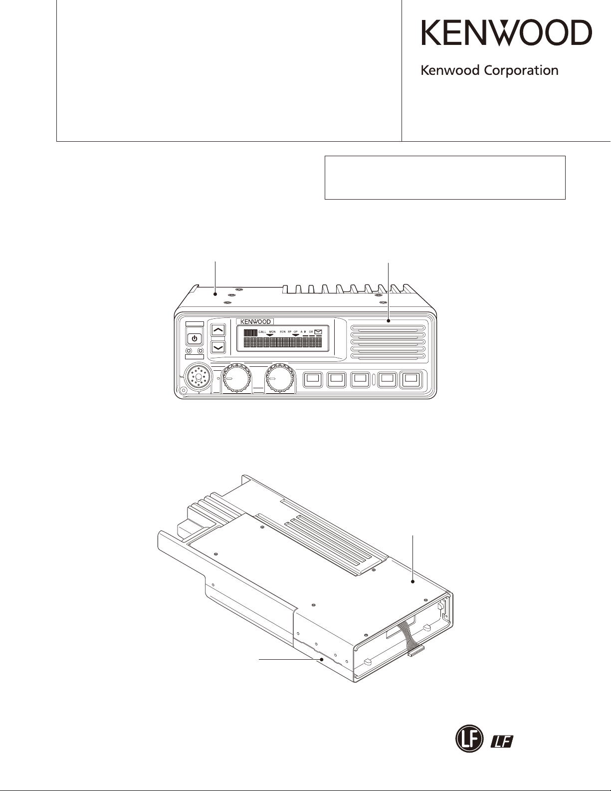
UHF P25 TRANSCEIVER
TK-5810(BG
TK-5810H(BG
SERVICE MANUAL
TK-5810(BG) with KCH-14
Metallic cabinet (Top)
(A01-2161-32)
POWER
GRP
)
)
© 2010-3 PRINTED IN JA PAN
B51-8913-00 (N
Use this service manual together with the KCH-14/15 service
manual (B51-8728-00) or KCH-16 service manual (B51-8834-00).
As for the hardware of this transceiver, version 3 is used.
The programming software must use KPG-95DG.
KCH-14
(Front panel kit)
)
TK-5810H(BG)
BUSY
TX
VOL
CH
Metallic cabinet (Top)
(A01-2163-21)
This product complies with the
Metallic cabinet (Bottom)
(A01-2164-31)
directive for the European market.
RoHS
This product uses Lead Free solder.

TK-5810(BG)/5810H(BG
)
CONTENTS
GENERAL ................................................................... 2
SYSTEM SET-UP ....................................................... 4
REALIGNMENT ......................................................... 5
INSTALLATION ........................................................ 12
DISASSEMBLY FOR REPAIR .................................. 20
CIRCUIT DESCRIPTION .......................................... 24
COMPONENTS DESCRIPTION ............................... 32
PARTS LIST ............................................................. 35
EXPLODED VIEW .................................................... 50
PACKING .................................................................. 52
TROUBLE SHOOTING ............................................ 54
ADJUSTMENT ........................................................ 56
Document Copyrights
Copyright 2010 by Kenwood Corporation. All rights re-
served.
No part of this manual may be reproduced, translated,
distributed, or transmitted in any form or by any means,
electronic, mechanical, photocopying, recording, or otherwise, for any purpose without the prior written permission
of Kenwood.
Disclaimer
While every precaution has been taken in the preparation
of this manual, Kenwood assumes no responsibility for errors or omissions. Neither is any liability assumed for damages resulting from the use of the information contained
herein. Kenwood reserves the right to make changes to any
products herein at any time for improvement purposes.
TERMINAL FUNCTION ........................................... 75
PC BOARD
FINAL UNIT (X45-3790-XX): TK-5810(BG) ......... 80
FINAL UNIT (X45-3800-XX): TK-5810H(BG) ...... 82
CONTROL UNIT (X53-4400-10) .......................... 86
TX-RX UNIT (X57-7270-XX) ................................ 90
INTERCONNECTION DIAGRAM ............................ 94
SCHEMATIC DIAGRAM .......................................... 96
BLOCK DIAGRAM ................................................. 114
LEVEL DIAGRAM .................................................. 120
SPECIFICATIONS .................................................. 121
Firmware Copyrights
The title to and ownership of copyrights for firmware
embedded in Kenwood product memories are reserved for
Kenwood Corporation. Any modifying, reverse engineering, copy, reproducing or disclosing on an Internet website
of the firmware is strictly prohibited without prior written
consent of Kenwood Corporation. Furthermore, any reselling, assigning or transferring of the fi rmware is also strictly
prohibited without embedding the firmware in Kenwood
product memories.
Transceivers containing AMBE+2™ Vocoder:
The AMBE+2™ voice coding technology is embedded in
the fi rmware under the license of Digital Voice Systems, Inc.
INTRODUCTION
SCOPE OF THIS MANUAL
This manual is intended for use by experienced technicians familiar with similar types of commercial grade communications equipment. It contains all required service
information for the equipment and is current as of the publication date. Changes which may occur after publication
are covered by either Service Bulletins or Manual Revisions.
These are issued as required.
2
GENERAL
ORDERING REPLACEMENT PARTS
When ordering replacement parts or equipment information, the full part identifi cation number should be included.
This applies to all parts: components, kits, or chassis. If the
part number is not known, include the chassis or kit number
of which it is a part, and a suffi cient description of the required component for proper identifi cation.

GENERAL
TK-5810(BG)/5810H(BG
)
PERSONAL SAFETY
The following precautions are recommended for personal
safety:
• DO NOT transmit if someone is within two feet (0.6 meter) of the antenna.
• DO NOT transmit until all RF connectors are secure and
any open connectors are properly terminated.
• SHUT OFF this equipment when near electrical blasting
caps or while in an explosive atmosphere.
• All equipment should be properly grounded before power-up for safe operation.
• This equipment should be serviced by only qualified
technicians.
PRE-INSTALLATION CONSIDERATIONS
1. UNPACKING
Unpack the radio from its shipping container and check
for accessory items. If any item is missing, please contact
KENWOOD immediately.
2. LICENSING REQUIREMENTS
Federal regulations require a station license for each
radio installation (mobile or base) be obtained by the equipment owner. The licensee is responsible for ensuring transmitter power, frequency, and deviation are within the limits
permitted by the station license.
Transmitter adjustments may be performed only by a
licensed technician holding an FCC fi rst, second or general
class commercial radiotelephone operator’s license. There is
no license required to install or operate the radio.
3. PRE-INSTALLATION CHECKOUT
3-1. Introduction
Each radio is adjusted and tested before shipment. How-
ever, it is recommended that receiver and transmitter operation be checked for proper operation before installation.
3-2. Testing
The radio should be tested complete with all cabling and
accessories as they will be connected in the fi nal installation. Transmitter frequency, deviation, and power output
should be checked, as should receiver sensitivity, squelch
operation, and audio output. Signaling equipment operation
should be verifi ed.
4. PLANNING THE INSTALLATION
4-1. General
Inspect the vehicle and determine how and where the
radio antenna and accessories will be mounted.
Plan cable runs for protection against pinching or crush-
ing wiring, and radio installation to prevent overheating.
4-2. Antenna
The favored location for an antenna is in the center of a
large, flat conductive area, usually at the roof center. The
trunk lid is preferred, bond the trunk lid and vehicle chassis
using ground straps to ensure the lid is at chassis ground.
4-3. Radio
The universal mount bracket allows the radio to be
mounted in a variety of ways. Be sure the mounting surface
is adequate to support the radio’s weight. Allow suffi cient
space around the radio for air cooling. Position the radio
close enough to the vehicle operator to permit easy access
to the controls when driving.
4-4. DC Power and wiring
1. This radio may be installed in negative ground electrical
systems only. Reverse polarity will cause the cable fuse
to blow. Check the vehicle ground polarity before instal-
lation to prevent wasted time and effort.
2. Connect the positive power lead directly to the vehicle
battery positive terminal. Connecting the Positive lead
to any other positive voltage source in the vehicle is not
recommended.
3. Connect the ground lead directly to the battery negative
terminal.
4. The cable provided with the radio is suffi cient to handle
the maximum radio current demand. If the cable must be
extended, be sure the additional wire is suffi cient for the
current to be carried and length of the added lead.
5.
INSTALLATION PLANNING – CONTROL STATIONS
5-1. Antenna system
Control station. The antenna system selection depends
on many factors and is beyond the scope of this manual.
Your KENWOOD dealer can help you select an antenna system that will best serve your particular needs.
5-2. Radio location
Select a convenient location for your control station radio which is as close as practical to the antenna cable entry
point. Secondly, use your system’s power supply (which
supplies the voltage and current required for your system).
Make sure suffi cient air can fl ow around the radio and power supply to allow adequate cooling.
SERVICE
This radio is designed for easy servicing. Refer to the
schematic diagrams, printed circuit board views, and alignment procedures contained in this manual.
NOTE
You must use KPG-95DG version 6.10 or later for this
transceiver.
3
TK-5810(BG)/5810H(BG
)
SYSTEM SET-UP
Before Reading About System Set-up
The TK-5810(BG)/5810H(BG) is a transceiver main unit
(without a panel or speaker) that you complete by adding
options.
The options are classifi ed into three types according to
operation and function.
Merchandise received
License and frequency allocated by FCC
Choose the type of transceiver
TK-5810(BG)/5810H(BG) is complete by combining options
with only the transceiver body (without panel)
Are you using the handheld control head?
NO
Are you using the remote kit?
NO
See page 12
Please refer to the
KCH-14/15 service manual
(B51-8728-00) for serving
information, such as circuit
diagram, parts list and etc.
KCH-14 (Basic model)
Front panel kit
Are you using the printed keytops?
See page 12
Supplied accessory keytops
YES
See page 12
Please refer to the
KCH-14/15 service manual
(B51-8728-00) for serving
information, such as circuit
diagram, parts list and etc.
KCH-15 (Full-featured
model) Front panel kit
YES
YES
NO
1. Install the front panel kit (controller) directly on a radio to
operate it. (Form: Radio + KCH-14/15)
2. Remotely control one radio with one controller. (Form:
Radio + KRK-5 + KCH-14/15 + KCT-22M/M2/M3)
3. Remotely control one radio with two controllers. (Form:
Radio + KRK-6DH + KCH-14/15 (two) + KCT-22M/M2/M3
(two))
Type
TK-5810H(BG) K
TK-5810H(BG) K2
Please refer to the KCH-16 service manual (B51-8834-00)
for serving information, such as circuit diagram,
installation, adjustment and etc.
Are you using one transceiver
with one controller?
See page 13
YES
Please refer to the
KRK-5/6DH service manual
(B51-8445-20) for serving
information, such as circuit
diagram, parts list and etc.
Single control head remote kit
KCH-14 KCH-15
Frequency range RF power
450~520MHz 45W~5WTK-5810(BG) K
400~470MHz 45W~5WTK-5810(BG) K2
450~500MHz 100W~50W
500~520MHz
400~470MHz
Are you using one radio with two controllers?
KRK-5
(Option) (Option)
60W~50W
100W~50W
YES
See page 15
Please refer to the
KRK-5/6DH service manual
(B51-8445-20) for serving
information, such as circuit
diagram, parts list and etc.
oror or
+
KRK-6DH
KCH-14
+
KCH-15
Dual control head remote kit
KCH-14
KCH-14
KCH-15
+
KCH-15
Service manual parts No. list
Model Parts No.
KRK-5/6DH B51-8445-20
KCH-14/15 B51-8728-00
KCH-16 B51-8834-00
4
Transceiver programming
KCT-23 DC cable
Are you using the voice guide & storage unit?
NO
Are you using the external speaker?
NO
Are you using the keypad microphone?
NO
Delivery
KCT-22M/M2/M3
Control cable
See page 5
A personal computer, programming interface (KPG-43/43A),
USB adapter (KCT-53U), and programming software
(KPG-95DG: ver. 6.10 or later) are required for programming.
(The frequency and signaling data are programmed for the transceiver.)
KCT-23 M,M3
YES
YES
YES
VGS-1
KES-5
KMC-28
See pages 14 and 15
See page 17
(Option)
See page 17
(Option)
(Option)
Desk top microphone KMC-9B
TK-5810(BG)/5810H(BG
REALIGNMENT
)
1. Modes
User mode
Panel test mode
PC mode
Firmware
programming mode
Firmware version information
Clock adjustment mode
Transceiver information mode
Clone mode
Self programming mode
Mode Function
User mode For normal use.
Panel test mode
Panel tuning mode Used by the dealer to tune the transceiver.
PC mode
Data programming
mode
PC test mode
Firmware
programming mode
Firmware version
information
Clock adjustment
mode
Transceiver
information mode
Clone mode
Self programming
mode
Used by the dealer to check the fundamental characteristics.
Used for communication between the
transceiver and PC.
Used to read and write frequency data and
other features to and from the transceiver.
Used to check the transceiver using the
PC. This feature is included in the FPU.
See panel tuning.
Used when changing the main program of
the fl ash memory.
Used to confi rm the internal fi rmware version.
Used by the dealer to adjust date and time.
Used to confi rm the transceiver fi rmware
version.
Used to transfer programming data from
one transceiver to another.
Frequency, signaling and features write to
the transceiver.
Panel tuning mode
Data programming mode
PC test mode
PC tuning mode
2. How to Enter Each Mode
Mode Operation
User mode Power ON
Panel test mode [PF1] + Power ON
PC mode Received commands from PC
Panel tuning mode [Panel test mode] + [GRP
Firmware programming mode [PF2] + Power ON
Firmware version information [PF3] + Power ON
Clock adjustment mode [PF4] + Power ON
Transceiver information mode [PF1] + [PF3] + Power ON
Clone mode [PF5] + Power ON
Self programming mode [GRP ] + Power ON
]
3. Panel Test Mode
Setting method refer to ADJUSTMENT.
4. Panel Tuning Mode
Setting method refer to ADJUSTMENT.
5. PC Mode
5-1. Preface
The transceiver is programmed by using a personal computer, programming interface (KPG-43/43A), USB adapter
(KCT-53U) and programming software (KPG-95DG: ver. 6.10
or later).
The programming software can be used with a PC. Figure 1 shows the setup of a PC for programming.
PC
KPG-43 or KPG-43A or
KPG-43A + KCT-53U
Illustration is KPG-43.
KPG-95DG
(Ver. 6.10 or later)
PC
D-SUB
(25-pin)
KPG-43
Transceiver
PC
D-SUB
(9-pin)
KPG-43A
Transceiver
PC
USB
KCT-53U
KPG-43A
Transceiver
Fig. 1
5
TK-5810(BG)/5810H(BG
)
REALIGNMENT
5-2. Connection procedure
1. Connect the transceiver to the computer using the interface cable and USB adapter (When the interface cable is
KPG-43A, the KCT-53U can be used.).
Note:
• You must install the KCT-53U driver in the computer to
use the USB adapter (KCT-53U).
• When using the USB adapter (KCT-53U) for the fi rst time,
plug the KCT-53U into a USB port on the computer with
the computer power ON.
2. When the POWER switch on, user mode can be entered
immediately. When PC sends command the transceiver
enter PC mode, and “PROGRAM” is displayed on the
LCD. When data transmitting from transceiver, the red
LED is lights. When data receiving to transceiver, the
green LED is lights.
Note:
The data stored in the computer must match the “Model
Name and Market Code” when it is written into the fl ash
memory.
5-3. KPG-43/KPG-43A description
(PC programming interface cable: Option)
The KPG-43/43A is required to interface the transceiver
to the computer. It has a circuit in its D-sub connector (KPG43: 25-pin, KPG-43A: 9-pin) case that converts the RS-232C
logic level to the CMOS level.
The KPG-43/43A connects the microphone jack of the
transceiver to the RS-232C serial port of the computer.
6. PC Tuning Mode
When making adjustment while in PC tuning mode,
modify the KPG-43/43A programming interface cable as described below.
1. Remove the two screws from the plug cover, then lift
the cover from the plug.
2. Solder the lead wire onto the MIC tab on the PCB, and
the ground wire onto the ME tab.
• KPG-43
++
C5
C4
Q1
MIC
MAX232C
ME
TRD
MAXIM
GND
SB
IC1
C7
+
5-4. KCT-53U description (USB adapter: Option)
The KCT-53U is a cable which connects the KPG-43A to
a USB port on a computer.
When using the KCT-53U, install the supplied CD-ROM
(with driver software) in the computer. The KCT-53U driver
runs under Windows 2000, XP or Vista (32-bit).
5-5. Programming software KPG-95DG description
The KPG-95DG (ver. 6.10 or later) is the programming
software for the transceiver supplied on a CD-ROM. This
software runs under Windows 98, ME, Windows NT4.0,
2000, XP or Vista (32-bit) on a PC.
The data can be input to or read from the transceiver and
edited on the screen. The programmed or edited data can
be printed out. It is also possible to tune the transceiver.
• KPG-43A
R3
Q1
D1
Q2
Q3
MIC
ME
C2
CN1
3.
• KPG-43
Create a hole in the casing (as shown in the illustration)
then fi t the cable into the hole. Replace the cover and
secure it using the two screws.
MIC
Cable
ME
Create a hole
6
TK-5810(BG)/5810H(BG
REALIGNMENT
)
• KPG-43A
Install the D-SUB socket into the cover after aligning the
lead wire as shown in the fi gure.
Replace the cover and secure it using the two screws.
D-SUB socket
Lead wire
MIC
ME
Cover
7. Firmware Programming Mode
7-1. Preface
Flash memory is mounted on the transceiver. This allows the transceiver to be upgraded when new features are
released in the future. (For details on how to obtain the fi rmware, contact Customer Service.)
• These transceivers use firmware versions G5.10 or
later. When using fi rmware versions earlier than version
G5.10, a “Check connection” error message will appear on the LCD. Firmware versions earlier than version
G5.10 will not write to the transceiver.
• While the firmware is being written, if the transceiver
resets due to a power supply interruption or other problem, the LCD may not display correctly (for example,
“PROGRAM FIRM” may not display).
Additionally, transceiver keys other than the power
switch cannot be operated.
To return to normal operation, click the “Cancel” but-
ton in the firmware programming software, then turn
the transceiver power OFF and back ON. “PROGRAM
FIRM” reappears on the display and the transceiver keys
can be operated. However, the previously written fi rmware data is lost; you must write the fi rmware using the
fi rmware programming software again.
8. Firmware Version Information
Press and hold the [PF3] key while turning the transceiv-
er power ON and then keep pressing and holding the [PF3]
key, the fi rmware version information appears on the LCD.
7-2. Connection procedure
Connect the transceiver to the personal computer (PC)
using the interface cable (KPG-43/43A) and USB adapter
(KCT-53U: When the interface cable is KPG-43A, the KCT53U can be used.). (Connection is the same as in the PC
Mode.)
7-3. Programming
1. Start up the fi rmware programming software (Fpro.exe).
2. Set the communications speed (normally, 115200 bps)
and communications port in the confi guration item.
3. Set the fi rmware to be updated by File name item.
4. Press and hold the [PF2] key while turning the transceiv-
er power ON. Then, the orange LED on the transceiver
lights and “PROGRAM FIRM” is displayed.
5. Check the connection between the transceiver and the
personal computer, and make sure that the transceiver is
in the Program mode.
6. Press “write” button in the window. When the trans-
ceiver starts to receive data, the [PG] display is blinking.
7. If writing ends successfully, the checksum is calculated
and a result is displayed.
8. If you want to continue programming other transceivers,
repeat steps 4 to 7.
Note:
• This mode cannot be entered if the Firmware Program-
ming mode is set to Disable in the Programming soft-
ware.
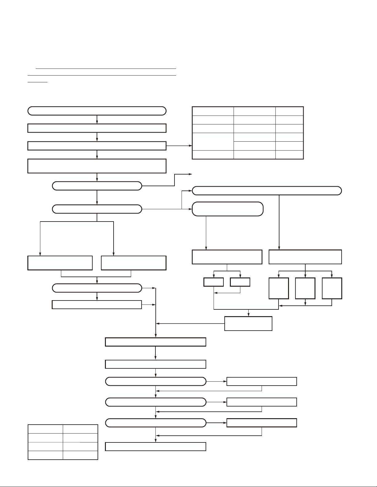
9. Clock Adjustment Mode
9-1. Flow chart of operation
[PF4] + Power ON
YEAR
MONTH
DAY
HOUR
MINUTE
[Selector] or [GRP ] and [GRP ]
[PF2]
[Selector] or [GRP ] and [GRP ]
[PF2]
[Selector] or [GRP ] and [GRP ]
[PF2]
[Selector] or [GRP ] and [GRP ]
[PF2]
[Selector] or [GRP ] and [GRP ]
[PF2]
Completion
10. Transceiver Information Mode
Use this function to confirm the transceiver firmware
version.
1. Press and hold the [PF1] and [PF3] keys while turning the
transceiver power ON.
2. The transceiver fi rmware version appears on the LCD.
3. To exit the transceiver information mode, turn the transceiver power OFF.
7
TK-5810(BG)/5810H(BG
)
REALIGNMENT
11. Clone Mode
Programming data can be transferred from one transceiver to another by connecting them via their microphone
jacks. The operation is as follows (the transmit transceiver
is the source and the receive transceiver is a target).
The following data cannot be cloned.
• Tuning data
• Embedded message with password
• Model name data
• ESN (Electronic Serial Number) data
• Network fi le data (P25)
Key guide on the “INPUT PASSWORD” display.
1. Press and hold the [PF5] key while turning the trans-
ceiver power ON. If the Read authorization password is
set to the transceiver, the transceiver displays “CLONE
LOCK”. If the password is not set, the transceiver dis-
plays “CLONE MODE”.
2. When you enter the correct password, and “CLONE
MODE” is displayed, the transceiver can be used as the
cloning source. The following describes how to enter
the read authorization password.
3.
• How to enter the read authorization password using
the microphone keypad;
If one of keys 0 to 9 is pressed while “CLONE LOCK” is
displayed, the pressed number is displayed on the LCD.
Each press of the key shifts the display in order to the
left.
If you press the [#] key, the least digit of the password is
deleted.
When you enter the password and press the [
“CLONE MODE” is displayed if the entered password is
correct. If the password is incorrect, “CLONE LOCK” is
redisplayed.
• How to enter the read authorization password using
the [Selector] knob;
If the [Selector] knob is rotated while “CLONE LOCK”
is displayed, the number (0 to 9) flashes on the LCD.
When you press the [GRP
number is determined. If you press the [PF3] key, the
least digit of the password is deleted. If you press the
[PF2] key after entering the password in this procedure,
“CLONE MODE” is displayed if the entered password is
correct. If the password is incorrect, “CLONE LOCK” is
redisplayed.
4. Power ON the target transceiver.
5. Connect the cloning cable (part No. E30-3370-05) to the
microphone jacks on the source and target.
6. Press the [PF2] key on the source while the source dis-
plays “CLONE MODE”. The data of the source is sent to
the target. While the target is receiving the data, “PRO-
GRAM” is displayed. When cloning of data is completed,
the source displays “END”, and the target automatically
operates in the User mode. The target can then be oper-
ated by the same program as the source.
] key, the currently selected
] key,
7. The other target can be continuously cloned. When
the [PF2] key on the source is pressed while the source
displays “END”, the source displays “CLONE MODE”.
Carry out the operation in step 4 to 6.
Note:
• You cannot clone transceivers using hardware versions
1.0 or 2.0.
Cloning is only possible when both transceivers are us-
ing hardware version 3.0.
• Cannot be cloned if the overwrite password is programmed to the target.
• “Model Name and Market Code”, “Head Confi guration”
and “Head Type” must be same to clone the transceiver.
However, it may be unable to clone the transceiver depending on the enhanced features settings.
(Refer to the FPU for the enhanced features details.)
• Under certain conditions, clone mode cannot be activated even if the clone mode of the source transceiver,
using Hardware Version 3.0, is set to enable. Refer to
the FPU for more details.
• Can not clone if the checksum in the Network File area
of the source transceiver and the target transceiver is different.
Cloning cable
(E30-3370-05)
8

TK-5810(BG)/5810H(BG
REALIGNMENT
)
12. Self Programming Mode
Write mode for frequency data and signaling etc. To be
used ONLY by the authorized service person maintaining the
user’s equipment. After programming, reset the FPU to the
“Self- Programming” disabled mode. Transceivers CANNOT
be delivered to the end-user in the self-programming mode.
The following setup items in the channels programmed
by the FPU can be changed using the self-programming
mode. The addition of new channel and the deletion of
channel that has already been programmed by the FPU cannot be performed using the self-programming mode.
• RX Frequency
• TX Frequency
• Channel Type (ANALOG or MIXED)
• TX Mode (When the channel type is selected “MIXED”.)
• Channel Spacing
• RX Signaling
• TX Signaling
• RX NAC
• TX NAC
• Talkgroup List No.
Note:
The personality will be also changed when the above-
mentioned items is changed. (Refer to the FPU for the
personality details.)
12-1. Enter to the self programming mode
Press and hold the [GRP ] key while turning the transceiver power ON. Ignoring whether the Read authorization
password is set or not, “PASSWORD” appears.
If the Read authorization password is not set to the transceiver, “SELF PG MODE” is displayed on the LCD when the
[PF2] key is pressed while “PASSWORD” is displayed.
If the password is set to the transceiver, “SELF PG
MODE” is displayed on the LCD when you enter the correct
password while “PASSWORD” is displayed.
For the password input method, see “11. Clone Mode”
step3 described on page 8.
Note:
This mode (self programming mode) cannot be set when
it has been disabled with the FPU.
12-2. Data writing
Before moving to the next Zone/Channel, “KEEP THIS
CHANGE?” appears on the LCD, if you select ”YES”, the
new data is written to memory. IF you select “NO”, the
new data will not be written; the new data will be erased.
12-3. Setup items for self programming mode
No. Setup item Display Remarks
1 Select Zone/Channel
2 RX Frequency
3 TX Frequency
4 Channel Type TYPE ANALOG/P25/MIXED
5 TX Mode MODE ANALOG/P25
6 Channel Spacing SPACE
7 RX Signaling RX-SIG Receive QT/DQT
8 TX Signaling TX-SIG Transmit QT/DQT
9 RX NAC RX-NAC
10 TX NAC TX-NAC
11 Talkgroup List No.
-
∗∗∗
∗∗∗
∗∗∗.∗∗∗∗∗
∗∗∗.∗∗∗∗∗
None When you do not want to set the Talkgroup list number to the transceiver.
∗∗∗
∗∗∗∗∗∗∗∗∗∗∗∗
MHz Receive frequency
MHz Transmit frequency
∗∗∗
∗∗∗
Zone: 1~100, Channel: 1~512
25.0kHz/12.5kHz (When the Channel type is selected “ANALOG” or “MIXED”.)
“P25 12.5kHz”
000~FFF (Hexadecimal) Note: “F7F” cannot be set.
000~FFF (Hexadecimal) Note: “F7E” and “F7F” cannot be set.
Talkgroup list number (1~250)
(When the Talkgroup list name is not set to the transceiver.)
Talkgroup list name (12 digits)
(When the Talkgroup list name is set to the transceiver.)
9
TK-5810(BG)/5810H(BG
)
REALIGNMENT
12-4. Key operation
• Normal mode
Key
[PF1] Unused
[PF2] Go to the next item
Zone-
Channel
RX
Frequency
TX
Frequency
Channel
Type
TX Mode
Channel
Spacing
RX
Signaling
TX
Signaling
RX NAC TX NAC
TG
List No.
Zone/
[PF3]
[PF4]
[PF5] Unused
[Selector]
[GRP
[GRP
MIC
keypad
([0] to [9])
MIC key-
pad ([
MIC key-
pad ([#])
MIC PTT Unused
Channel
switching
Data Writ-
Channel
up/ down
]
Channel up
]
Channel
Unused
])
ing
Zone/
Zone/
Zone/
down
5kHz/ 6.25kHz/ 1MHz
step switching
Unused
1step up/ down Unused Signaling up/ down
Go to the MIC keypad
ON/ OFF
switching
1step up Unused Signaling up
1step down Unused Signaling down Unused
input mode
ANALOG/
P25/
MIXED
switching
Unused
ANALOG/
P25
switching
Unused
Unused
Channel
Spacing
switching
Unused
1step/ Standard
switching
QT/ DQT(N)/ DQT(I)/
OFF switching
Go to the MIC keypad
input mode
Delete the least digit
from the current number (Press and hold to
delete all numbers.)
Unused
Increment/ Decrement
a number in the speci-
fi ed digit
Determine the least
digit
Add a digit to the cur-
rent number
Delete the least digit
from the current number (Press and hold to
delete all numbers.)
[PTT] + [2]: “A”
[PTT] + [5]: “B”
[PTT] + [8]: “C”
[PTT] + [0]: “D”
[PTT] + [#]: “E”
[PTT] + [
]: “F”
Unused
TG List
number
up/ down
TG List
number up
TG List
number
down
Unused
Unused
Unused
• MIC keypad input mode
Key RX Frequency TX Frequency RX Signaling TX Signaling
[PF1] Cancel the MIC keypad input mode (Return to the normal mode)
[PF2] Cancel the MIC keypad input mode (Return to the normal mode)
[PF3] Delete the least digit from the current number (Press and hold to delete all numbers.)
[PF4] Unused ON/ OFF switching QT/ DQT(N)/ DQT(I)/ OFF switching
[PF5] Unused
[Selector] Unused
[GRP
[GRP
MIC keypad ([0] to [9]) Add a digit to the current number (Return to the normal mode automatically if all digit are entered.)
MIC keypad ([
MIC keypad ([#]) Delete the least digit from the current number (Press and hold to delete all numbers.)
] Unused
] Unused
]) Cancel the MIC keypad input mode (Return to the normal mode)
MIC PTT Unused
10
12-5. Self programming mode fl ow chart
TK-5810(BG)/5810H(BG
REALIGNMENT
)
[PF2]
[TX Frequency]: “OFF”
[Channel Type]: “ANALOG”
[PF2]
[Channel Type]: “ANALOG”
[GRP ] + Power ON
Self programming mode
KEEP THIS CHANGE
[PF2]: “YES” or
[PF1]: “NO”
[PF2]
[Channel Type]: “P25”
[PF2]
[TX Frequency]: “OFF”
or
[Channel Type]: “ANALOG” or “MIXED”
[PF2]
[TX Frequency]: “OFF”
[Channel Type]: “P25” or “MIXED”
or
[TX Frequency]: Other than “OFF”
[Channel Type]: “MIXED”
[TX Mode]: “P25”
Input Password
Read authorization password entry (6 digits)
[PF2]
[PF2]
Zone/Channel
[PF2]
RX Frequency
[PF2]
TX Frequency
[PF2]
Channel Type
[PF2]
[TX Frequency]: Other than “OFF”
[Channel Type]: “MIXED”
TX Mode
[PF2]
Channel Spacing
[PF2]
RX Signaling
[PF2]
[TX Frequency]: Other than “OFF”
[Channel Type]: “ANALOG” or “MIXED”
[TX Mode]: “ANALOG”
TX Signaling
[PF2]
[Channel Type]: “MIXED”
[PF4]
Zone selection
OFF
ANALOG
ANALOG
25.0kHz
[PF3]
[PF3]
[PF3]
[PF4] [PF4]
OFF
[PF4] [PF4]
OFF
[PF3]
Channel selection
[PF3]
[PF3]
P25 MIXED
P25
12.5kHz
[PF4]
QT DQT N
[PF4]
QT DQT N
[PF4]
[PF4]
DQT I
DQT I
[PF2]
[TX Frequency]: “OFF”
Squelch Type*
or
[TX Frequency]: Other than “OFF”
[Channel Type]: “MIXED”
[TX Mode]: “ANALOG”
Squelch Type*1: “NAC”
[PF2]
Talkgroup ID List Amount: 0
*1: The squelch type can not be set using the self-programming mode.
1
: “NAC”
[PF2]
[TX Frequency]: “OFF”
Talkgroup ID List Amount must not be 0.
or
[TX Frequency]: Other than “OFF”
[Channel Type]: “MIXED”
[TX Mode]: “ANALOG”
Talkgroup ID List Amount must not be 0.
Talkgroup List No.
RX NAC
[PF2]
[TX Frequency]: Other than “OFF”
[Channel Type]: “P25” or “MIXED”
If [Channel Type] is set to “MIXED”,
[TX Mode] must be set to “P25”.
TX NAC
[PF2]
[Channel Type]: “P25” or “MIXED”
Talkgroup ID List Amount must not be 0.
[PF2]
11
TK-5810(BG)/5810H(BG
)
INSTALLATION
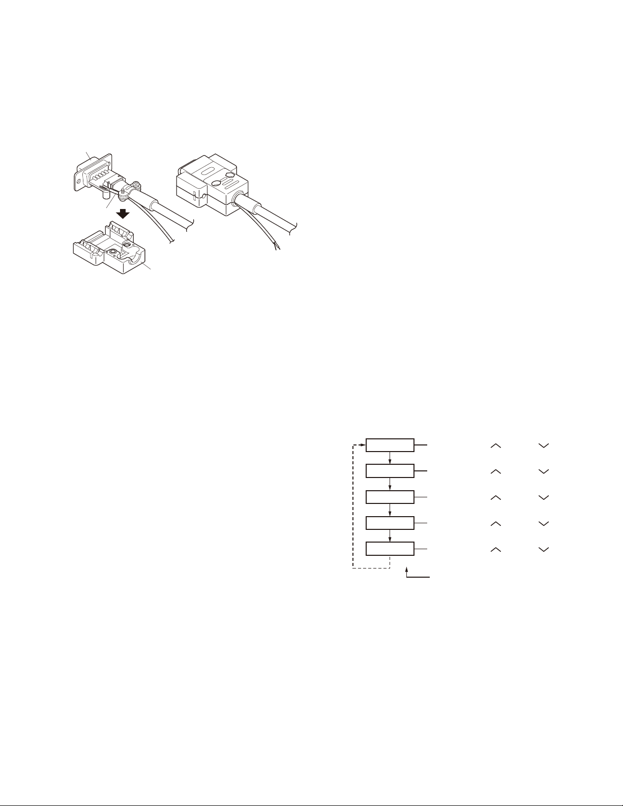
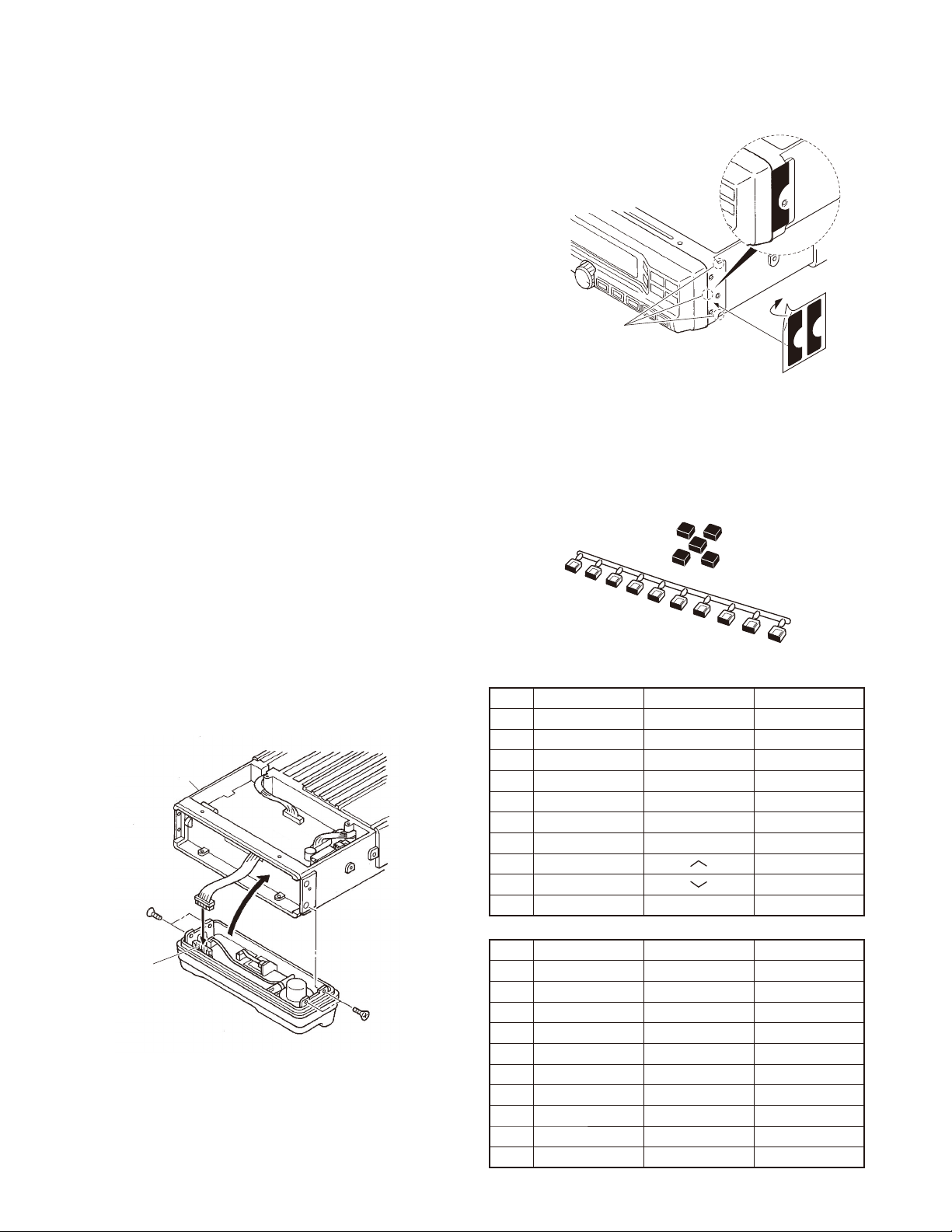
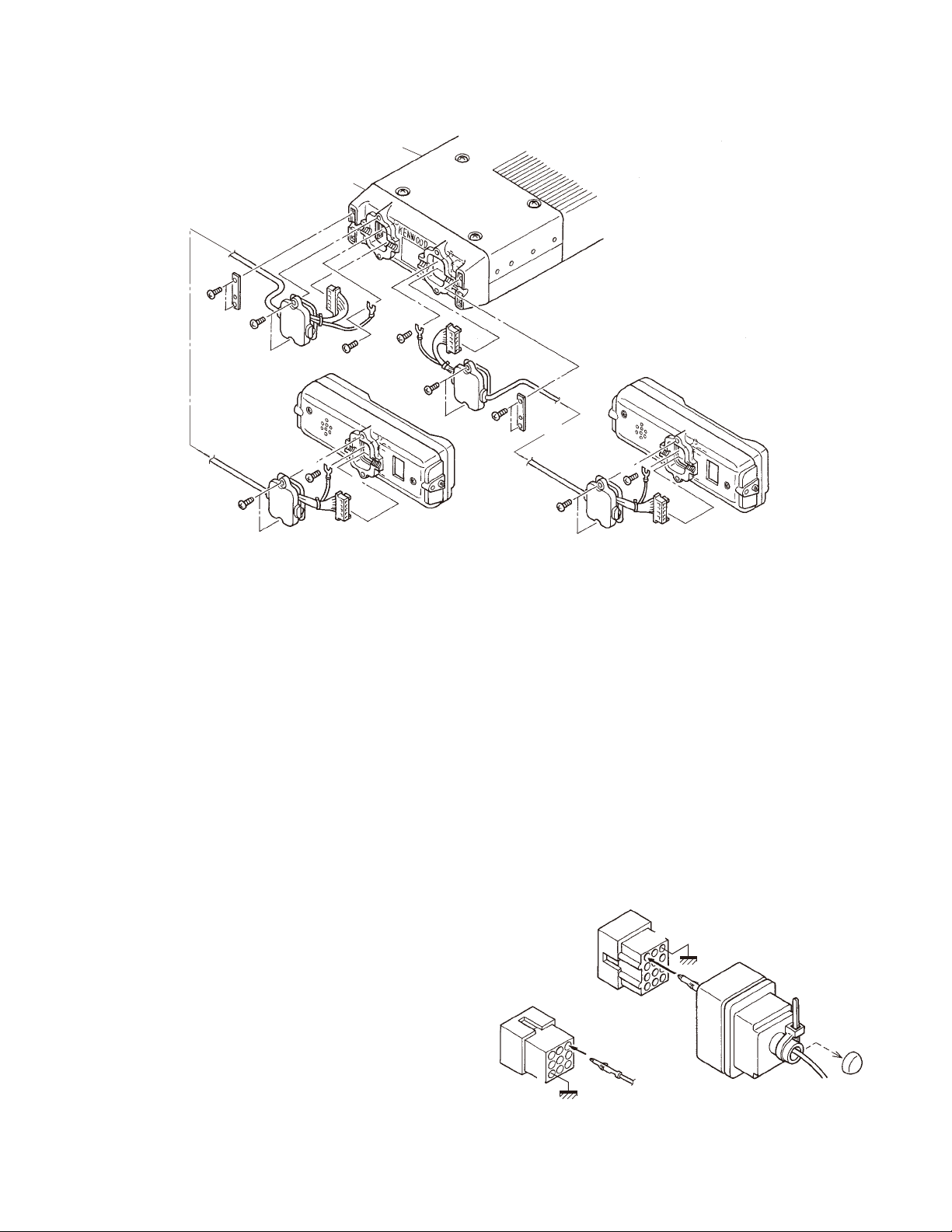
1. Front Panel Kit (KCH-14/15: Option)
1-1. Installing the KCH-14/15 front panel kit to the
transceiver
1. Remove the upper case and lower case of the transceiver.
2. Insert the lead wire with connector (W700) of the control
unit (X53-440) into the connector (CN1) of the KCH-14 or
KCH-15.
3. Install the KCH-14 or KCH-15 on the transceiver using
the four screws q supplied with the front panel kit.
Note:
Take care that the lead wire with connector (W700) is
not caught when fitting the KCH-14 or KCH-15 on the
transceiver. (You can install the panel upside down if necessary to install the transceiver.)
4. Affixing the sheet (G11-4379-04) for the waterproof
(Fig.1-1-2).
(1) Remove the covering paper of the sheet w.
(2) Affi x the sheet while taking note of the position of the
three parts as shown in Fig.1-1-2 e.
Firmly affi x the sheet to the chassis by pushing the
double-coated tape with your fi ngers.
(3) Repeat step (2) to affi x the sheet to the other side of
chassis.
Note:
The sheet cannot be reused. Affix a new sheet when
you removed the sheet.
5. Reassemble the upper case and lower case. (Refer to
page 18)
Note:
Take care that the sheet (G11-4379-04) is not peeled off
when installing the upper/lower case.
6. Connect the short plug to the accessory connector (9-pin)
on the rear of the transceiver.
Transceiver
W700
:
@
Affix the sheet while
taking note of the position
of the three parts.
.
Fig. 1-1-2
1-2. Installing the accessory keytops to the front
panel kit
When a function is set by the programming software
(KPG-95DG), the key legend can be changed by inserting
the accessory keytops into PF1 to PF9 of the KCH-15 (PF1
to PF5: KCH-14). The accessory contains 60 keytops as
shown the table below.
1
2
3
4
5
6
7
8
9
Fig. 1-2
No. K29-5276-03 K29-5277-03 K29-5305-03
1 AN RCL CH1
2 D/A RPT CH2
3 DIM SCN CH3
4 HA SP CH4
5 HC SPM CH5
6 IC SQ AUX A
7 MON TA AUX B
8 OPT
9 OST
10 PA No printing
10
AUX C
EMG
■
12
CN1
KCH-14 or
KCH-15
Fig. 1-1-1
No. K29-9353-13 K29-9354-13 K29-9356-03
1 2TN GPS PAG
2 AD STS SIT
:
3 AR TAC SRC
4 CLK TON No printing
5 FNC RES No printing
6 PBK IDV No printing
7 SCP KDL No printing
8 SEC TGR No printing
9 SEL RGP No printing
10 SES No printing No printing
TK-5810(BG)/5810H(BG
INSTALLATION
)
KCH-14
POWER
TX
BUSY
KCH-15
POWER
TX
BUSY
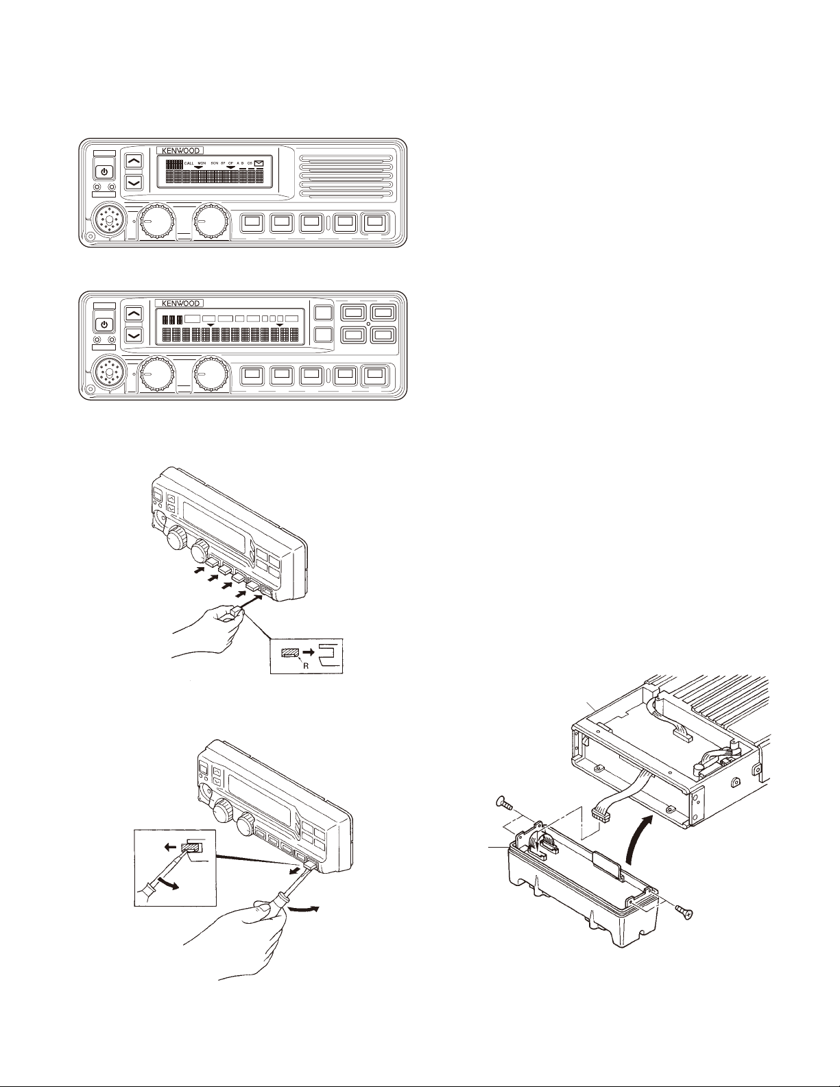
2. Remote kit (KRK-5: Option)
The KRK-5 remote kit is used to remotely operate the
GRP
VOL
GRP
VOL
CALL
CH
PF1 PF2 PF3 PF4 PF5
SCAN OPT OSTA B CMON
SP
CH
PF1 PF2 PF3 PF4 PF5
MON
PF7PF6
SCN
PF9PF8
Fig. 1-3
transceiver. The KRK-5 is connected to the KCH-14 or KCH15 with an optional KCT-22M (8 feet), KCT-22M2 (17 feet),
or KCT-22M3 (25 feet) control cable.
2-1. Installing the KRK-5 main panel onto the
transceiver
1. Remove the upper case and lower case of the transceiver.
2. Insert the lead wire with connector (W700) of the control
unit (X53-440) into the connector (CN4) of the KRK-5.
3. Install the KRK-5 main panel on the transceiver using
four screws q.
Note:
Take care that the lead wire with connector (W700) is not
caught when fi tting the KRK-5 main panel on the transceiver.
4. Affixing the sheet (G11-4379-04) for the waterproof
(Fig.2-1-2).
(1) Remove the covering paper of the sheet w.
(2) Affi x the sheet while taking note of the position of the
three parts as shown in Fig.2-1-2 e.
Firmly affi x the sheet to the chassis by pushing the
double-coated tape with your fi ngers.
(3) Repeat step (2) to affi x the sheet to the other side of
chassis.
Note:
The sheet cannot be reused. Affix a new sheet when
you removed the sheet.
5. Reassemble the upper case and lower case of the transceiver. (Refer to page 18)
Note:
Take care that the sheet (G11-4379-04) is not peeled off
when installing the upper/lower case.
Fig. 1-4 Keytop insertion
Fig. 1-5 Keytop removal
Packing
Transceiver
:
CN4
KRK-5 main panel
W700
:
Fig. 2-1-1
13
TK-5810(BG)/5810H(BG
)
INSTALLATION
KRK-5 main panel
@
Affix the sheet while
taking note of the position
of the three parts.
Fig. 2-1-2
.
2-3. Control cable (KCT-22) connection (Fig. 2-3)
1. Insert one connector of the control cable to the transceiver (with KRK-5) and the other to the display. Connect
the cable to the GND terminal with the screw q supplied with the control cable.
2. Secure the one connector of the control cable to the
KRK-5 main panel with two screws w according to the
installation condition of the transceiver. Secure the control cable to the KRK-5 main panel with the cable fi tting
(J21-4354-04) and two screws e supplied with the KRK-
5.
3. Secure the other connector of the control cable to the
display with two screws r in the same way.
2-2. Installing the KRK-5 rear panel onto the front
panel kit
The following steps apply to both the KCH-14 and KCH-15.
1. Remove three screws q on the KRK-5 rear panel, then
remove the KRK-5 sub panel.
2. Insert the lead wire with connector (W102) of the KRK-5
into the connector (CN1) of the front panel kit w.
3. Insert the lead wire with connector (W103) of the KRK-5
into the connector (CN3) of the front panel kit e.
4. Make a slight cut in the end of the rubber cap r.
5. Slide the lead wire of the connector wiring t through
the slit in the rubber cap y.
6. Insert the rubber cap into the hole of the KRK-5 rear
panel u.
7. Insert the connector i to the ACC connector o on the
KRK-5 sub panel as shown by the arrow !0.
8. Install the KRK-5 sub panel onto the sub panel of the
front panel kit !1.
9. Install the KRK-5 sub panel to the sub panel of the front
panel kit using four screws !2.
10. Reinstall the KRK-5 rear panel using three screws removed in step 1.
11. Use a wire band to secure the lead wire at the end of the
rubber cap !3.
Front panel kit
(Example : KCH-14)
Packing
Sub panel
Transceiver
KRK-5 main panel
.
Cable
fitting
@
:
Control cable
KCT-22
GND
Display
:
GND
;
Fig. 2-3
2-4. Display installation (Fig. 2-4)
1. Install the display with the angle bracket (J29-0648-03)
and two screws (N08-0526-04) w supplied with the
q
KRK-5.
14
Rubber
cap
CN1
CN3
.
W103
1
;
2
3
=
Make
a cut
@
W102
IGN,
GND etc.
8
B
Fig. 2-2
>
KRK-5 sub panel
KRK-5 rear panel
Lead wire
IGN,GND etc.
@
:
:
Angle
bracket
@
Fig. 2-4
TK-5810(BG)/5810H(BG
INSTALLATION
)
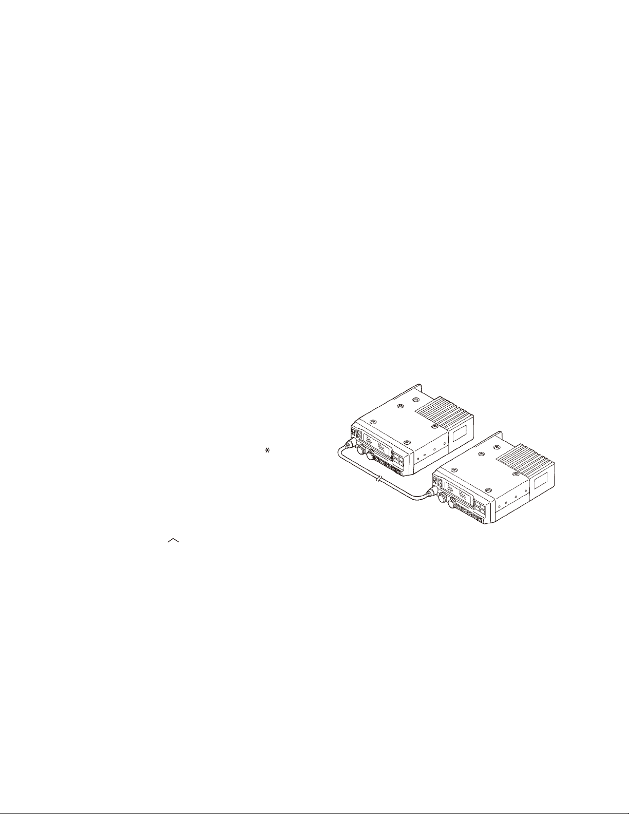
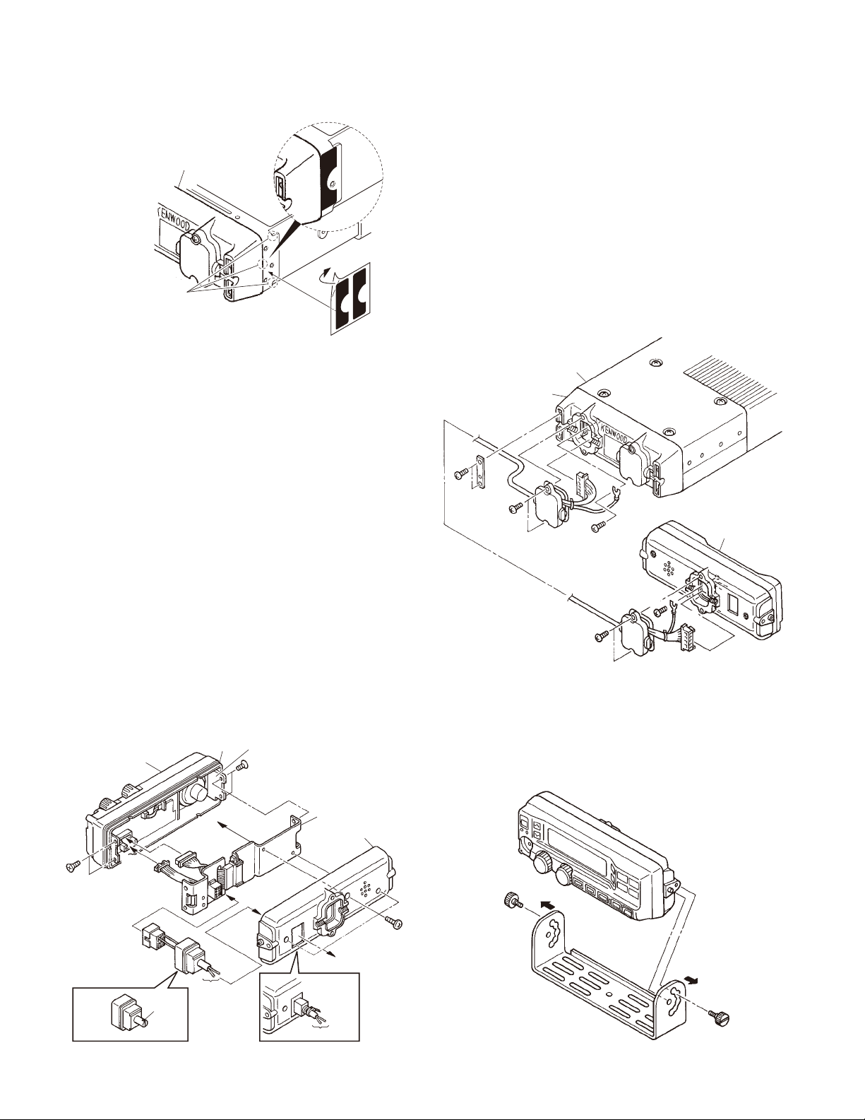
3. Dual Control Head Remote Kit
(KRK-6DH: Option)
The KRK-6DH remote kit connects two displays (two
KCH-14s or KCH-15s) to the transceiver. The KRK-6DH is
connected to the KCH-14s or KCH-15s with two optional
control cables. There are three version of the control cable:
KCT-22M (8 feet), KCT-22M2 (17 feet), and KCT-22M3 (25
feet).
3-1. Installing the KRK-6DH main panel onto the
transceiver
1. Remove the upper case and lower case of the transceiv-
er.
2. Insert the lead wire with connector (W700) of the control
unit (X53-440) into the connector (CN4) of the KRK-6DH.
Insert the lead wire with connector (W104) of the KRK-
6DH into the connector (CN503) of the transceiver.
3. Install the KRK-6DH main panel on the transceiver using
four screws q.
Note:
Take care that the lead wire with connector (W700) is
not caught when fi tting the KRK-6DH main panel on the
transceiver.
4. Affixing the sheet (G11-4379-04) for the waterproof
(Fig.3-1-2).
(1) Remove the covering paper of the sheet w.
(2) Affi x the sheet while taking note of the position of the
three parts as shown in Fig.3-1-2 e.
Firmly affi x the sheet to the chassis by pushing the
double-coated tape with your fi ngers.
(3) Repeat step (2) to affi x the sheet to the other side of
chassis.
Note:
The sheet cannot be reused. Affix a new sheet when
you removed the sheet.
5. Reassemble the upper case and lower case of the trans-
ceiver. (Refer to page 18)
Note:
Take care that the sheet (G11-4379-04) is not peeled off
when installing the upper/lower case.
Transceiver
CN503
:
W104
CN4
CN5
KRK-6DH
main panel
W700
:
Fig. 3-1-1
KRK-6DH main panel
@
Affix the sheet while
taking note of the position
of the three parts.
.
Fig. 3-1-2
3-2. Installing two KRK-6DH rear panels onto two
front panel kits
Install each KRK-6DH rear panel onto each front panel
kit as same as “2-2.Install the KRK-5 rear panel onto the
front panel kit” described on page 14.
3-3. Control cable (KCT-22) connection (Fig. 3-2)
1. Use two control cables. Insert one connector of the one
control cable to the transceiver (with KRK-6DH) and the
other to the display 1.
Insert one connector of the other control cable to the
transceiver (with KRK-6DH) and the other to the display 2.
Connect each cable to the GND terminal with the screws
supplied with each control cable.
q
2. Secure the one connector of each control cable to the
KRK-6DH main panel with two screws w according to
the installation condition of the transceiver. Pass the control cables through the grooves at both ends of the KRK6DH main panel and secure the control cables to the
KRK-6DH with the cable fitting (J21-4354-04) and two
screws e supplied with the KRK-6DH.
3. Secure the other connectors of the control cables to the
display 1 and display 2 with two screws r in the same
way.
15
TK-5810(BG)/5810H(BG
)
INSTALLATION
Transceiver
KRK-6DH
main panel
.
Cable
fitting
@
:
Display 1
GND
:
GND
@
.
Display 2
Cable
fitting
KCT-22
Control cable
:
GND
;
4. Ignition Sense Cable (KCT-18: Option)
The KCT-18 is an optional cable to use the following func-
tions:
• Ignition function
The ignition function allows you to turn the transceiver's
power on and off with the ignition key of your car. When
you are driving with the ignition key on, the horn alert function is disabled.
• Timed power-off function
The timed power-off function turns the transceiver's
power off the time specified with the programming software (KPG-95DG) after the ignition key is turned off. When
you are driving with the ignition key on, the horn alert function is disabled.
The ignition sense function and the timed power-off
function can be used at the same time.
KCT-22
Control cable
Fig. 3-2
:
GND
;
4-2. Connecting the KCT-18 cable to the
KRK-5/6DH remote kit
1. Remove the square plug from the accessory connector
(12-pin) on the rear of the control head.
2. Cut off the end of the rubber cap (accessory), insert the
KCT-18 lead terminal into the rubber cap, and insert it
into pin 1 (IGN) of the square plug.
3. Connect the square plug and rubber cap to the accessory
connector (12-pin) on the rear of the control head, then
clamp the bottom of the rubber cap with the supplied tie
wrap.
Note:
You must setup using the KPG-95DG.
Square plug
(12-pin)
3
1
Rubber cap
4-1.
Connecting the KCT-18 cable to the transceiver
1. Remove the short plug from the accessory connector (9pin) on the rear of the transceiver.
2. Insert the KCT-18 lead terminal into pin 1 (IGN) of the
short plug (9-pin).
3. Connect the short plug to the accessory connector (9-pin)
on the rear of the transceiver.
Note:
You must setup using the KPG-95DG.
16
12
Short plug
(9-pin)
7
9
1
3
10
KCT-18
Fig. 4-1 Fig. 4-2
Tie wrap
Cut
KCT-18
TK-5810(BG)/5810H(BG
INSTALLATION
)
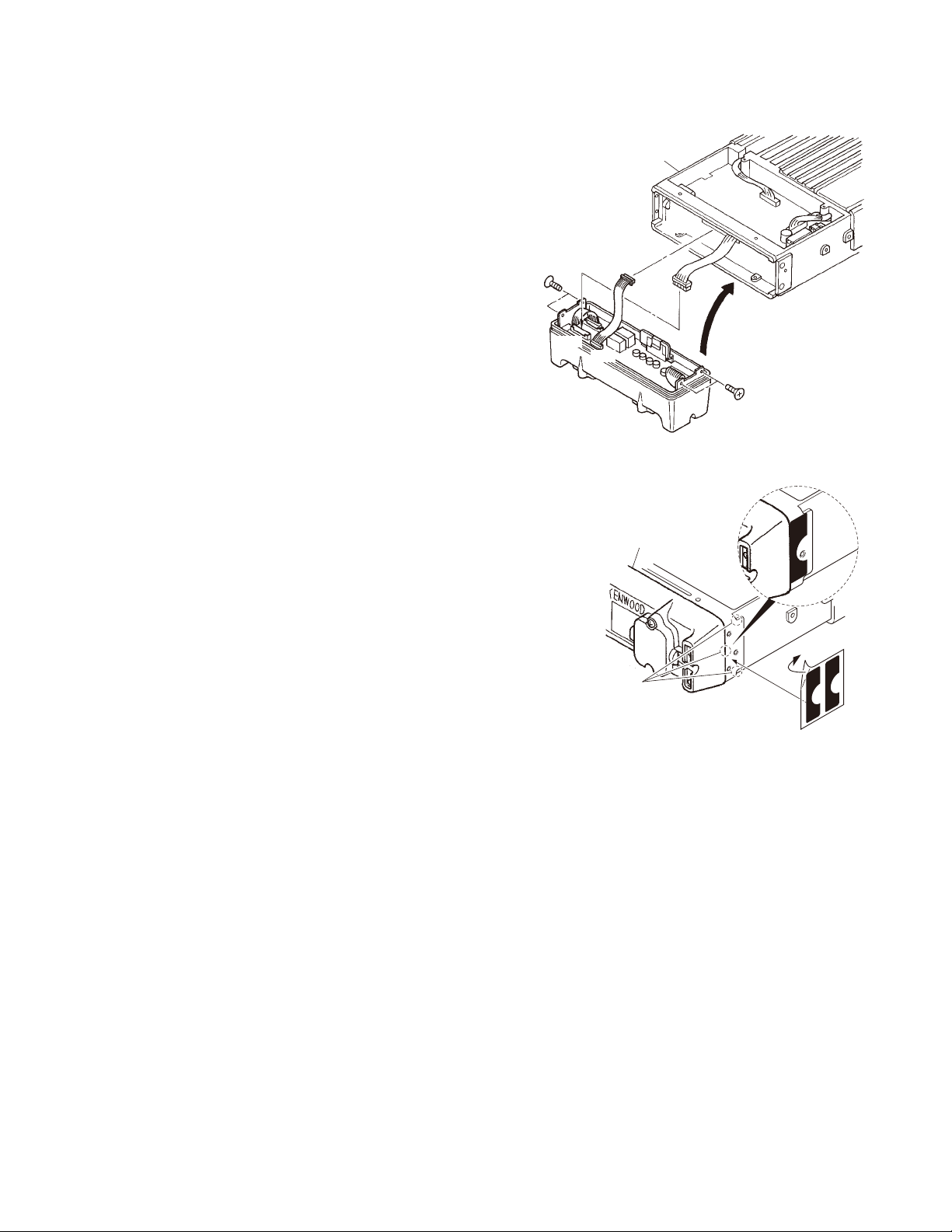
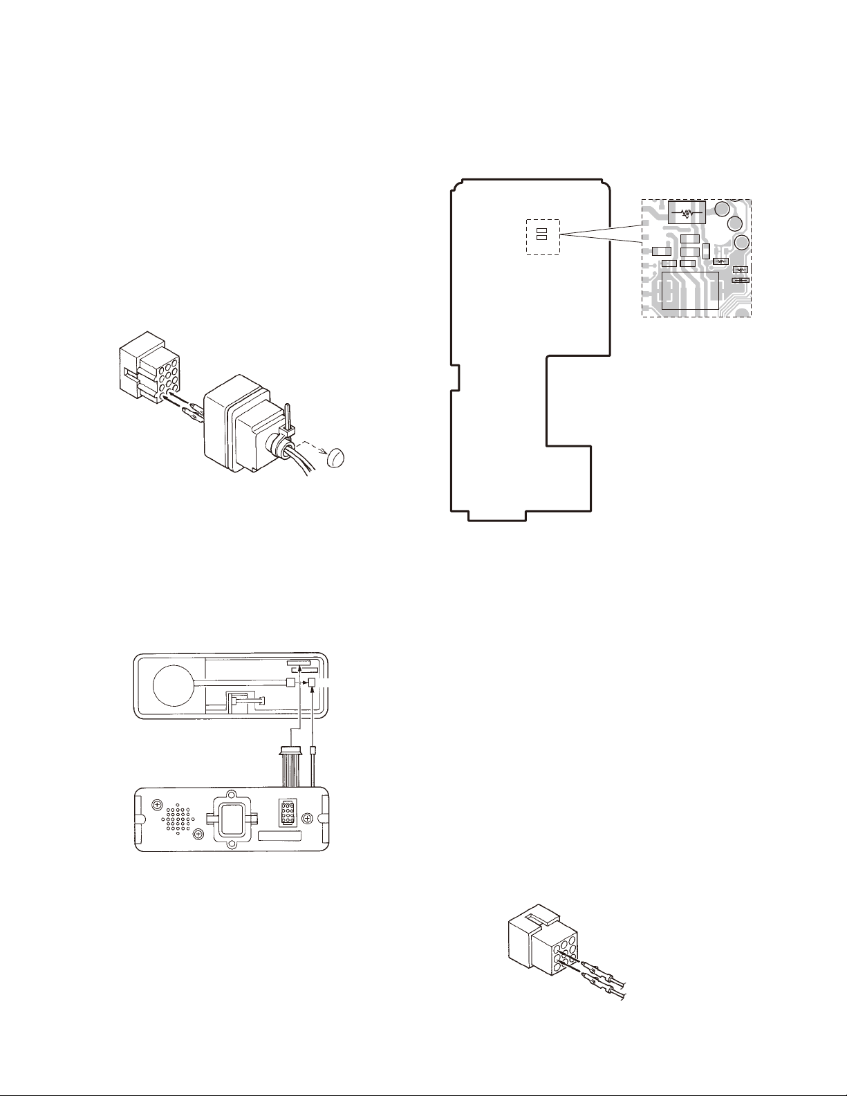
5. Voice Guide & Storage Unit
(VGS-1: Option)
5-1. Installing the VGS-1 unit in the transceiver
1. Remove the upper case and upper packing of the transceiver.
2. Attach two cushions to the VGS-1 as shown in fi gure.
Note:
Be sure not to cover the VGS-1 connector (CN1) with the
cushion.
3. Insert the VGS-1 connector (CN1) into the control unit
connector (CN411).
Note:
You must setup using the KPG-95DG.
VGS-1
Cushion
(G13-1992-04)
21 x 21 x 2.5mm
Cushion
(G13-1974-04)
21 x 21 x 1.0mm
CN1
6-1. Connecting the KES-5 external speaker to the
transceiver
• When taking the AF output from the accessory connector (9-pin) on the rear of the transceiver
The following tools are required for changing the connec-
tor.
Extracting tool
The following extracting tool is recommended :
Molex Inc. Order No.: 11-03-0002
1. Remove the short plug from the accessory connector (9pin) on the rear of the transceiver (Fig. 6-1-1).
Note: Save the jumper, which is required when the trans-
ceiver is used without the external speaker.
2. Remove the terminals with the jumper from the connector housing holes number 3 and 6 using the extracting
tool.
Removing the jumper lead (Fig. 6-1-2)
1) Insert the extracting tool (11-03-0002) into the con-
nector while pushing the jumper lead in the direction
of (a).
2) Push the extracting tool into collapse the barbs of the
crimp terminal.
3) Pull out the lead while continuing to push the extract-
ing tool in the direction (b).
3. Reinsert the terminal with the black and white stripe lead
into hole number 2, and the terminal with the black lead
into hole number 6 (Fig. 6-1-3).
4. Connect the short plug to the accessory connector (9-pin)
on the rear of the transceiver.
(a)
CN411
Fig. 5
6. External Speaker (KES-5: Option)
The speaker output from the transceiver is as follows:
1. The KCH-14 has a built-in speaker (3W/8 ohms).
2. The KCH-15 does not have a built-in speaker.
3. The external speaker output from the accessory connector (9-pin) on the rear of the transceiver is 13W/4 ohms.
Use the KES-5.
4. The speaker output from the accessory connector (12pin) on the rear of the control head is 2W/4 ohms. If the
remote kit (KRK-5, KRK-6DH) is used, use the KES-5.
Note:
Since the transceiver uses a BTL audio amplifi er, do not
ground the speaker output pin.
Short plug
(E37-0733-05)
Extracting tool
(11-03-0002)
Crimp terminal
Fig. 6-1-1 Fig. 6-1-2
Short plug
(9-pin)
1
7
9
2
To KES-5
6
Black/White lead
Black lead
Fig. 6-1-3
(b)
Jumper lead
Barbs
17
TK-5810(BG)/5810H(BG
)
INSTALLATION
6-2. Connecting the KES-5 external speaker to the
KRK-5/6DH remote kit
• When taking the AF output from the 12-pin accessory connector on the rear of the control head
• Modifi cation of plug (12-pin)
1. Remove the square plug from the accessory connector
(12-pin) on the rear of the control head.
2. Cut off the end of the rubber cap, insert the KES-5
speaker cable into the cap, and insert it into pins 10 and
11 of the square plug.
3. Connect the square plug and rubber cap to the accessory
connector (12-pin) on the rear of the control head, then
clamp the bottom of the rubber cap with the supplied tie
wrap.
Square plug (12-pin)
11
10
Rubber cap
Tie wrap
Cut
Speaker cable
(To KES-5)
Fig. 6-2-1
Note:
Even if the KRK-6DH is modifi ed in this way, the audio
output of head 2 cannot be increased.
SB
ES2
$R73
R74
CN2
KCH-14
DISPLAY UNIT (X54-349 A/3)
Foil side view
NC
• If the KCH-14 is used
If the KES-5 is connected to the 12-pin accessory con-
nector, remove the internal speaker wire.
If the internal speaker is used, remove the wire connect-
ed to pins 10 and 11 of the 12-pin accessory connector.
KCH-14
CN3
SP
CN1
Rear of the control head
CN2
Fig. 6-2-2
6-3. Modifi cation to increase the audio output of
the control head
The speaker output can be increased to 13W by moving
jumper resistor (0 ohm) R74 to $R73 on the KCH-14 display
unit (X54-349 A/3). In this case, the KCH-14 internal speaker
cannot be used because the maximum input (3W) of the internal speaker is exceeded. Therefore, use the KES-5.
18
Fig. 6-3
6-4. Use as public address speaker
1. Remove the short plug from the 9-pin accessory connector on the rear of the transceiver. (Remove the jumper
lead as described in Section 6-1 on page 17.)
2. Insert the KES-5 speaker leads into pins 7 and 8 of the
short plug.
3. If you remove jumper shorting pins 3 and 6, the 20W PA
(public address) voice signal is output from pins 7 and 8.
(Only when the PA or SP switch is on.)
4. If you use the transceiver shorted with pins 3 and 6, the
internal speaker is available (when the KCH-14 is used).
The KCH-15 does not contain a speaker.
Note:
Relationship between accessory connector (9-pin) con-
nection and speaker output.
When pins 3 and 6 are shorted; The 3W internal speaker
is used (KCH-14 only).
When pins 3 and 6 are opened and is output from pins 7
and 8; The 20W external speaker is used.
Short plug (9-pin)
7
8
Crimp terminal
(E23-0613-05)
To KES-5
Black lead
Black/White lead
Fig. 6-4
TK-5810(BG)/5810H(BG
INSTALLATION
)
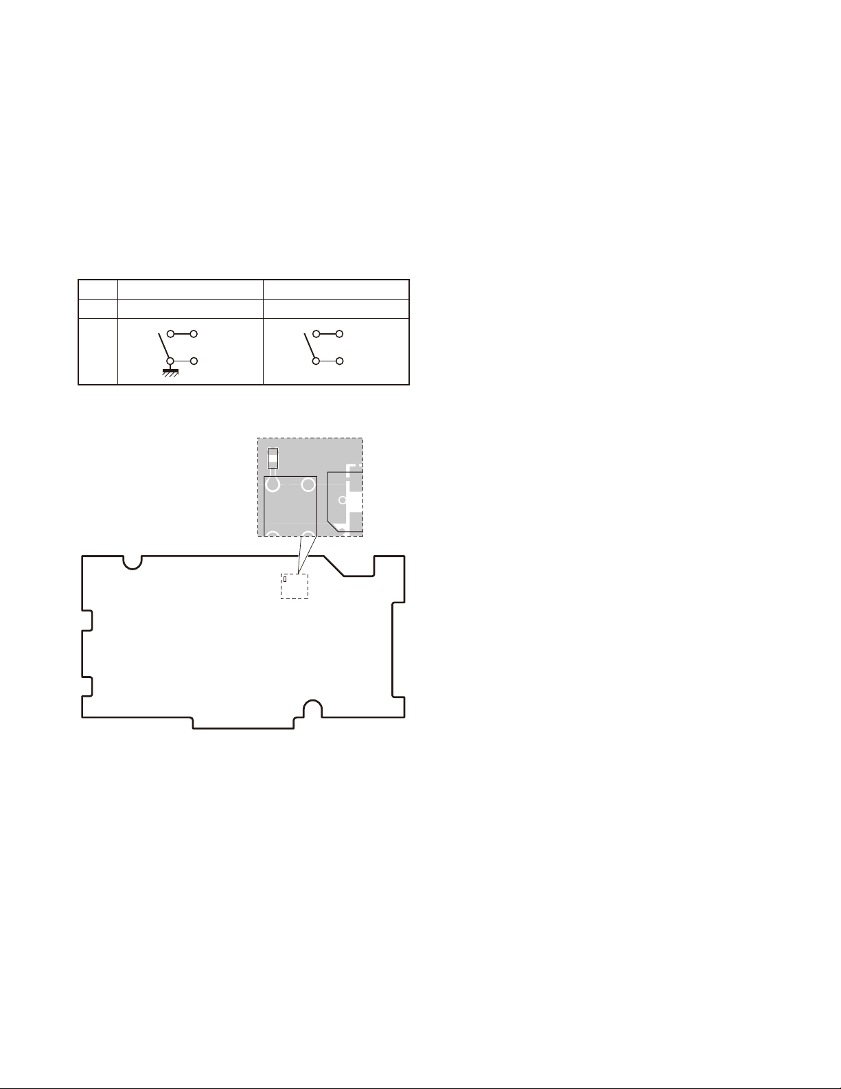
7. Horn Alert Function
The HR1 and HR2 pins of the accessory connector (9pin) on the rear of the transceiver are connected to the relay
(K500) and the maximum current is 1A.
1. Remove the upper case of the transceiver.
2. To make the HR2 pin, remove the jumper resistor (0
ohm) R634 on the control unit (X53-440) as shown in
Table 1.
3. Reassemble the PC board and the upper case.
Default Modifi cation
R634 Present Absent
State
HR1
HR2
Table 1
R634
K500
HR1
HR2
C6
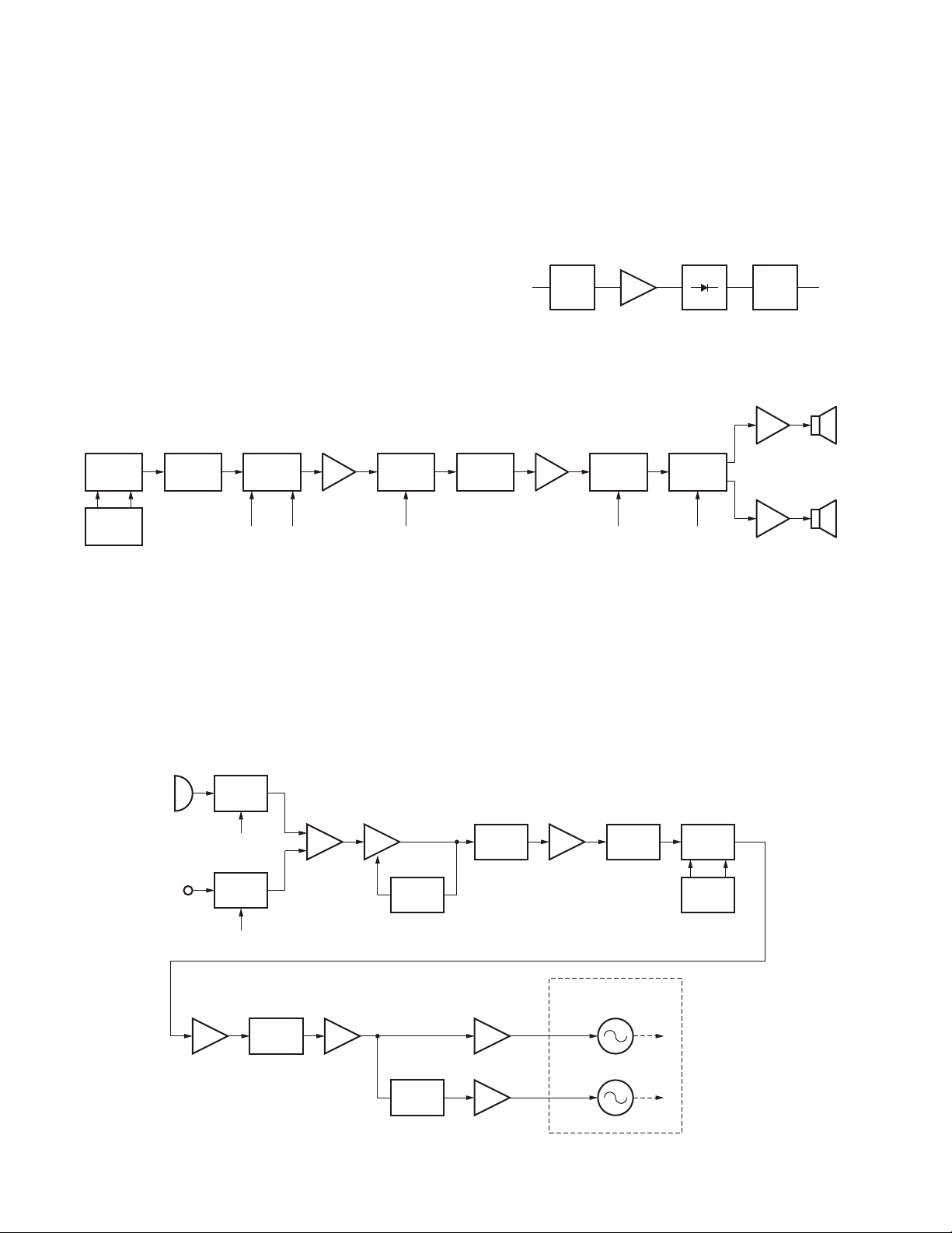
8. Handheld control head
(KCH-16: Option)
The KCH-16 Handheld control head is used to remotely
operate the transceiver.
See the service manual No. B51-8834-00
CONTROL UNIT (X53-440)
Component side view
Fig. 7
19
TK-5810(BG)/5810H(BG
)
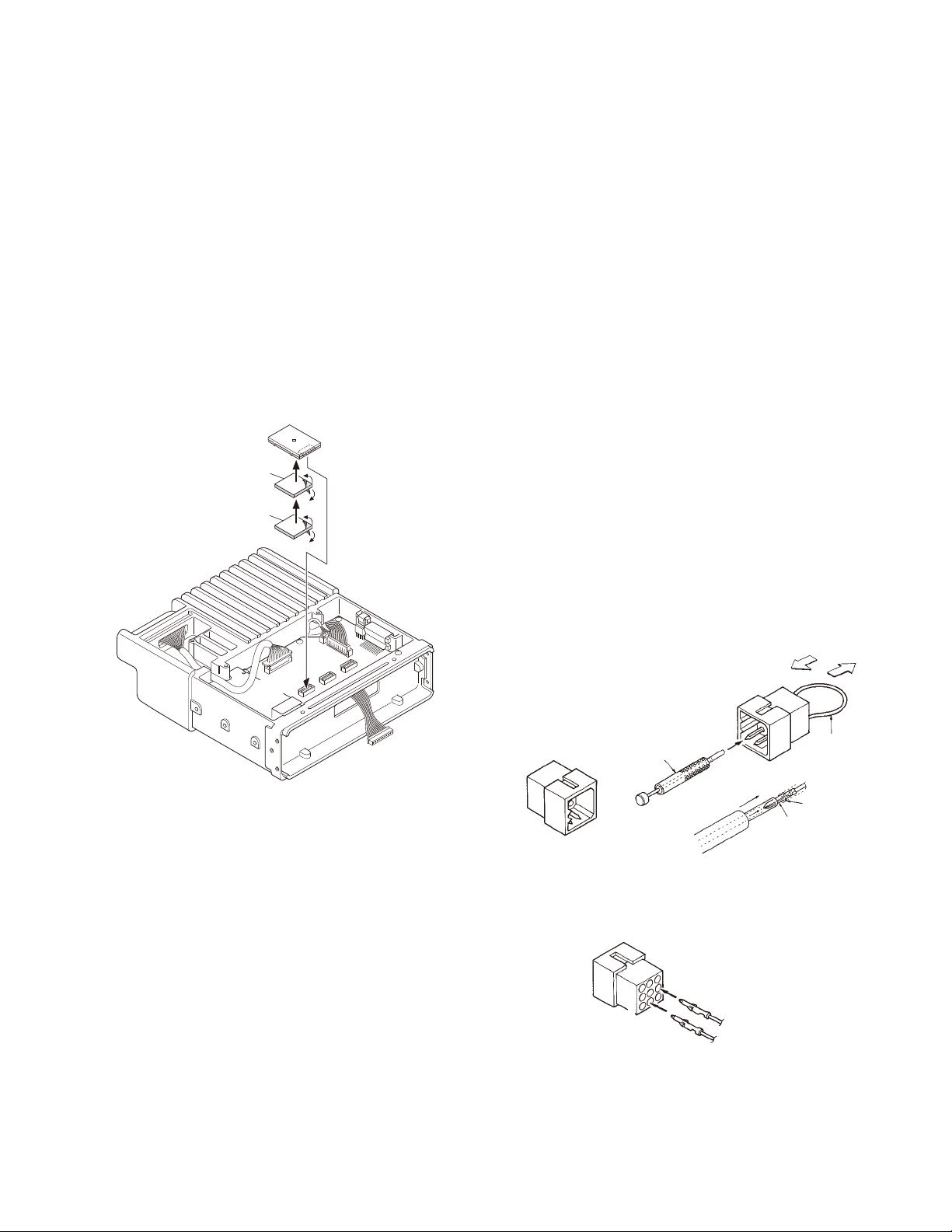
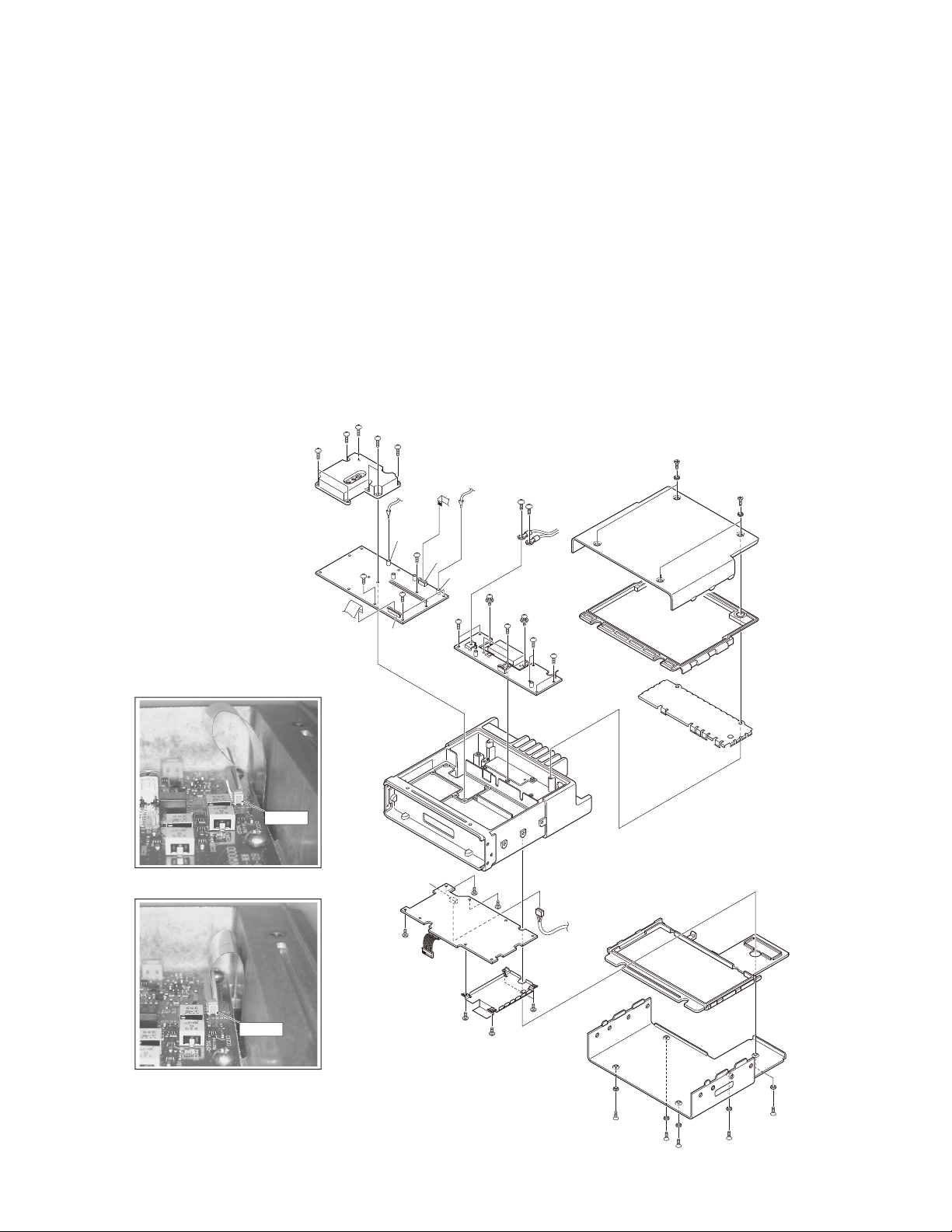
DISASSEMBLY FOR REPAIR
Disassembly Procedure (TK-5810(BG))
Removing the upper/lower case and shielding cover
■
1. Remove the 9 screws q and 9 spacers w.
2. Remove the upper case e and lower case r.
3. Remove the upper packing t and lower packing y.
4. Remove the shielding cover u.
Removing the TX-RX unit (X57-727)
■
1. Remove the 7 screws i holding the PLL shielding cover.
2. Remove the PLL shielding cover o.
3. Remove the coaxial cables from the two connectors
(CN151 and CN200) of the TX-RX unit !0.
4. Remove the fl at cables from the two connectors (CN600
and CN601) of the TX-RX unit !1.
2
2
2
2
TX-RX
unit
8
2
CN151
CN601
CN600
CN200
Note:
When re-installing the fl at cable to the connector on the
CN600 side, do not align the cable as shown in the fi gure
1, as there is a possibility of producing an effect on the
sensitivity of P25.
5. Remove the 5 screws !2.
Removing the Final unit (X45-379)
■
1. Remove the cables from the connector (CN1) of the control unit !3.
2. Remove the 2 screws !4 holding the power module.
3. Remove the solder of the power module with a solder
absorber.
4. Remove the 2 screws !5 holding the + (positive) terminal
and – (negative) terminal of the power supply cable.
5. Remove the 8 screws !6 holding the fi nal unit.
6. Remove the solder of the antenna receptacle with a solder absorber.
:
@
;
B
:
@
Wrong
Right
CN600
CN600
CN1
Control
unit
Final unit
>
=
.
@
@
2
:
@
:
:
:
@
@
:
20
TK-5810(BG)/5810H(BG
DISASSEMBLY FOR REPAIR
)
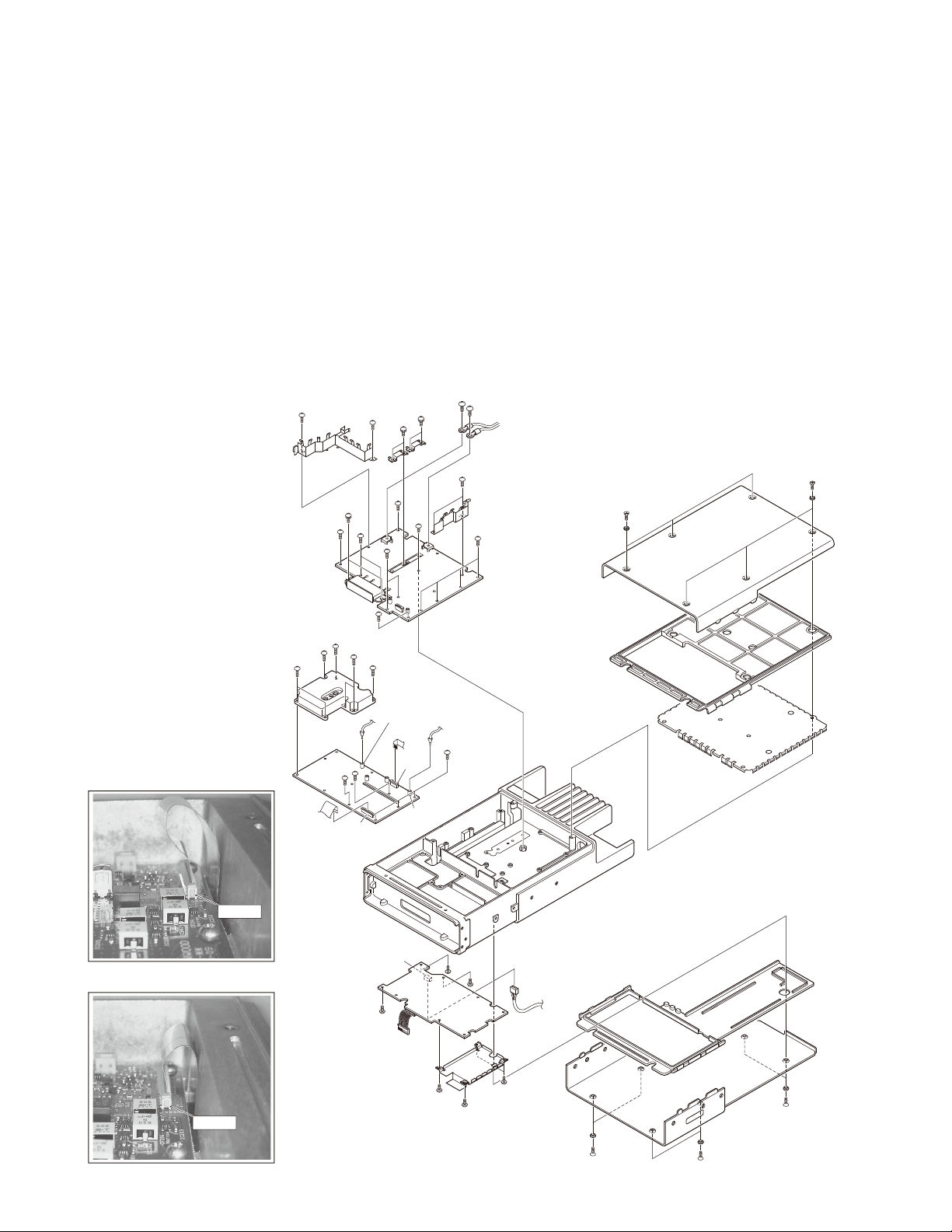
Disassembly Procedure (TK-5810H(BG))
Removing the upper/lower case and shielding cover
■
1. Remove the 12 screws q and 12 spacers w.
2. Remove the upper case e and lower case r.
3. Remove the upper packing t and lower packing y.
4. Remove the shielding cover u.
Removing the TX-RX unit (X57-727)
■
1. Remove the 7 screws i holding the PLL shielding cover.
2. Remove the PLL shielding cover o.
3. Remove the coaxial cables from the two connectors
(CN151 and CN200) of the TX-RX unit !0.
4. Remove the fl at cables from the two connectors (CN600
and CN601) of the TX-RX unit !1.
Note:
When re-installing the fl at cable to the connector on the
CN600 side, do not align the cable as shown in the fi gure
1, as there is a possibility of producing an effect on the
sensitivity of P25.
5. Remove the 5 screws !2.
Removing the Final unit (X45-380)
■
1. Remove the cables from the connector (CN1) of the control unit !3.
2. Remove the 2 screws !4 holding the power module.
3. Remove the solder of the power module with a solder
absorber.
4. Remove the 4 screws !5 holding the two final transistors.
5. Remove the 2 screws !6 holding the + (positive) terminal
and – (negative) terminal of the power supply cable.
6. Remove the 16 screws !7 holding the fi nal unit.
7. Remove the solder of the antenna receptacle with a sol-
der absorber.
:
@
;
:
@
Wrong
Right
CN600
2
2
8
TX-RX
unit
2
CN600
CN200
Final unit
Control
unit
B
>
=
2
2
CN151
CN601
CN1
CN600
.
@
:
@
:
@
:
21
TK-5810(BG)/5810H(BG
)
DISASSEMBLY FOR REPAIR
Disassembly Procedure (TK-5810(BG)/5810H(BG))
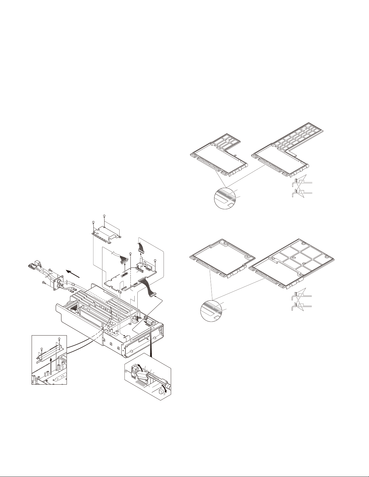
Removing the Control unit (X53-440)
■
1. Remove the 7 screws q.
2. Remove the shielding plate w.
3. With a fl at-head screwdriver, remove the 2 fl at springs
holding the ICs (IC5 and IC522) e.
4. Remove the fl at cable from the connector (CN501) r.
5. Remove the cables from the two connectors (CN459 and
CN502) t.
Removing the accessory cable and power sup-
■
Precautions for Reassembly
■
Paint the lubricant to the position as shown in fi gure af-
Note:
To assure waterproofing, paint the lubricant on the
• Case packing (Upper)
TK-5810 TK-5810H
ply cable on the rear of the transceiver
1. Confi rm the following contents.
• The screws holding the + (positive) terminal and –
(negative) terminal of the power supply cable is removed.
• The cable from the connector (CN502) of the Control
unit is removed.
2. Remove the 4 screws y holding the shielding plate,
and remove the shielding plate u from the chassis (TK5810H(BG) only).
3. Remove the 4 screws i on the rear of the transceiver.
4. Pull out the power supply cable and accessory cable.
:
:
• Case packing (Lower)
@
:
:
=
2
2
B
B
>
CN459
=
CN502
CN501
;
TK-5810 TK-5810H
Painting the lubricant (Part No.: 410-0019-05) on
the groove of the case packing
ter replacing or assembling the case packing.
groove of the case packing.
lubricant
lubricant
case packing
Paint the lubricant (Part No.410-0019-05)
on the groove of the case packing.
lubricant
case packing
Paint the lubricant (Part No.410-0019-05)
on the groove of the case packing.
OK
NG
OK
NG
groove of the
case packing
lubricant
groove of the
case packing
22
Flat
spring
IC
.
TK-5810(BG)/5810H(BG
DISASSEMBLY FOR REPAIR
)
Align the cable connecting the W2 terminal:
■
TK-5810H(BG) only
When you assemble the fi nal unit, align the cable con-
necting the W1 terminal as shown in fi gure, then insert it
into the connector (CN1) of the control unit.
Accessory
cable
W1 terminal
cable
CN1
W1
Control
unit
Final unit
W1 terminal
cable
• Case packing (Lower)
TK-5810H
TK-5810
Sequence of tightening the screws for the up-
■
per/lower case to the chassis
Install the upper/lower case to the chassis and tighten
the screws in the order shown in the fi gure below.
• Case case
TK-5810H
Procedures after installing the case packing to
■
the chassis
After installing the case packing to the chassis, confi rm
that all corners of the upper/lower packing are securely
fi tted to the chassis. Place are shown in the arrow in the
fi gure below.
• Case packing (Upper)
TK-5810H
TK-5810
TK-5810
3
1 2
•Lower case
TK-5810
3 4
5 6
5
4
3
1 2
TK-5810H
5 6
3 4
4
1 2
1 2
23
TK-5810(BG)/5810H(BG
)
CIRCUIT DESCRIPTION
1. Overview
This transceiver is a UHF/FM/P25 transceiver designed
to operate in the frequency range of 450 to 520MHz (K) or
400 to 470MHz (K2).
The unit consists of receiver, transmitter, phase-locked
loop (PLL) frequency synthesizer, base band parts, power
supply, and control circuits.
ANT
TX/RX: 450~520MHz (K)
TX/RX: 400~470MHz (K2)
ANT
SW
PA
AMP
RF
AMP
TX
AMP
1st MIX
400.05~470.05MHz(K)
350.05~420.05MHz(K2)
450~520MHz (K)
400~470MHz (K2)
MCF
49.95MHz
16.8MHz
VCXO
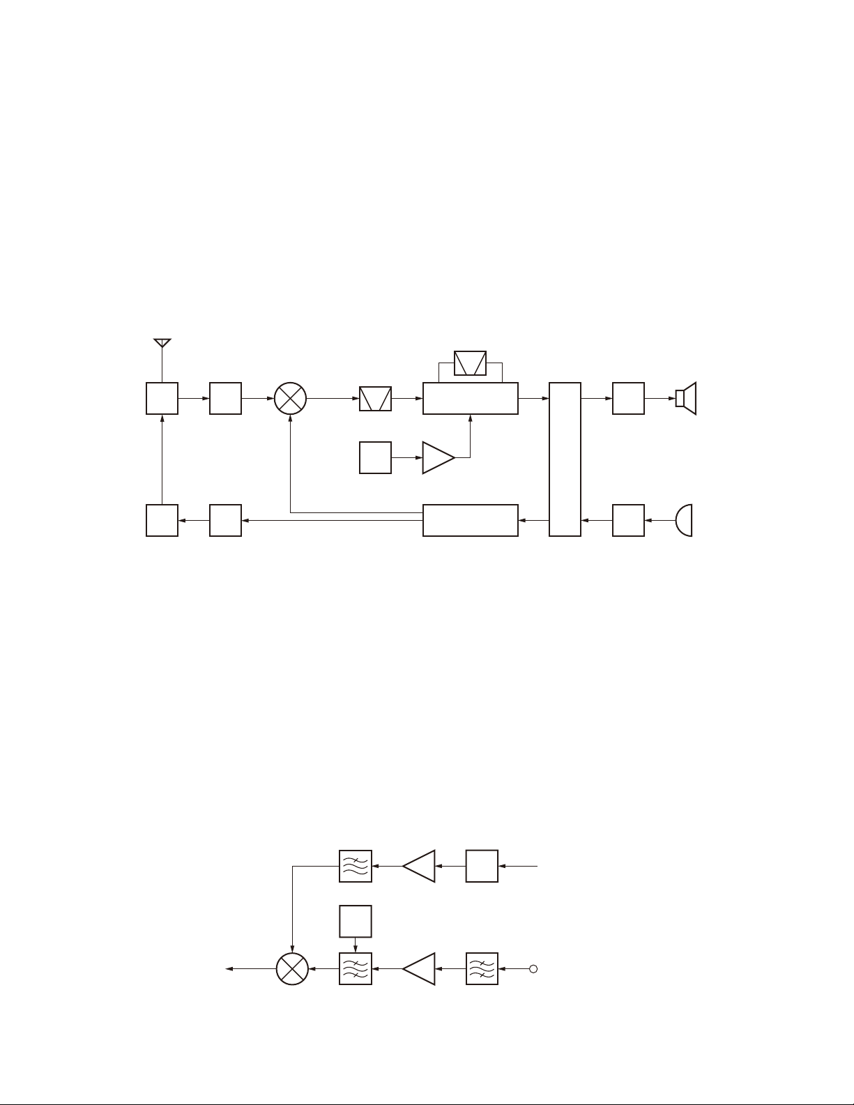
2. Frequency Confi guration
The receiver is a double-conversion superheterodyne
using fi rst intermediate frequency (IF) of 49.95MHz and second IF of 450kHz. Incoming signals from the antenna are
mixed with the local signal from the PLL circuit to produce
the fi rst IF of 49.95MHz.
This is then mixed with the 50.4MHz second local oscillator output to produce the 450kHz second IF. This signal is
detected to give the demodulated signal in the DSP.
The transmit signal frequency is generated by the PLL
VCO, and modulated by the signal from the DSP. It is then
amplifi ed and fed to the antenna.
CF
450kHz
SP
MIX
IF AMP
x3
50.4MHz
PLL
VCO
ASIC
A/D
D/A
DSP
AF
AMP
MIC
MIC
AMP
Fig. 1 Frequency confi guration
3. Receiver System
3-1. Front-end RF Amplifi er
The receive signal from the RX terminal (CN200) of the
TX-RX unit (X57-727) is amplifi ed by a transistor (Q200) and
passes through the band-pass fi lter (L207, L208, L209 and
L210) to remove unwanted signal.
The signal passing through the band-pass fi lter goes into
the 1st mixer.
These band-pass fi lters are tuned to a desired frequency
by variable capacitance diode (D204, D205, D206 and D207).
Local AMP
LPF
D204,D205,D206,D207
VC
TUNE
1st MIXER
1st IF
49.95MHz
IC200
BPF
L207,L208,L209,L210
Q203
RF AMP
Q200
LNA
A tuning voltage corresponding to the desired signal is
applied to each variable capacitance diode to tune to the receive frequency.
3-2. 1st Local
The 1st mixer uses double balanced mixer (IC200).
The receive signal passing through the band-pass fi lter
(L207, L208, L209 and L210) and the 1st local signal generated by the VCO, are mixed by the 1st mixer (IC200) to produce a 1st IF signal (49.95MHz) (Lower heterodyne).
VCO
1st Local OSC
400.05~470.05MHz (K)
350.05~420.05MHz (K2
RX terminal (CN200)
450~520MHz (K)
400~470MHz (K2)
)
24
Fig. 2 Front-end RF amplifi er and 1st local

TK-5810(BG)/5810H(BG
CIRCUIT DESCRIPTION
)
3-3. 1st IF
The 1st IF signal passes through the MCF (Monolithic
Crystal Filter) to remove unwanted signal.
The MCF has two paths (Wide band: XF201, Narrow
band: XF200), and these are controlled with the IF filter
switch (D208, D209, D210, D211, D212, D213, D214 and
D215).
The signal passes through the MCF (XF201) when the
Wide band (D209, D211, D213 and D215 are ON) is selected. The signal passes through the MCF (XF200) when
the Narrow band (D208, D210, D212 and D214 are ON) is
selected.
2nd IF
450kHz
2nd Local
50.40MHz
IC209
FM IC
Tripler
Q207
Q205 Q204
VCXO
D214
D215
X200
16.8MHz
WIDE
XF201
NARROW
XF200
SW
Fig. 3 1st IF and 2nd local
The 1st IF signal passing through these MCFs is amplified by the IF amplifier (Q205) and goes into the FM IC
(IC209).
3-4. 2nd Local
The 1st IF signal (49.95MHz) amplifi ed by the IF amplifi er (Q205) and the 2nd local signal (50.4MHz) generated by
tripling the reference oscillator frequency (16.8MHz) of the
VCXO (X200) by Q207, are mixed in the FM IC (IC209) to
produce a 2nd IF signal (450kHz) (Upper heterodyne).
WIDE
XF201
D212
D213
SW
D210
D211
SW
NARROW
XF200
D208
D209
SW
1st IF
49.95MHz
3-5. 2nd IF
The 2nd IF signal passes through the ceramic fi lter to re-
move unwanted signal.
The ceramic fi lter has two paths (Wide band: CF201 and
CF202, Narrow/P25 band: CF200 and CF204), and these
are controlled with the multiplexers (IC201, IC202, IC203,
IC205, IC206 and IC207).
The control line is W/N1, W/N2 and VN.
WIDE
CF201
IC205
W/N2 W/N2
SW
IC206
SW
NARROW/P25
CF200
DET
L234
FM/P25 DET
DET
COIL
IC201
SW
IC202
SW
The signal passes through the ceramic fi lters (CF201 and
CF202) when the Wide band (W/N1: high level, W/N2: high
level, VN: high level) is selected. The signal passes through
the ceramic filters (CF200 and CF204) when the Narrow/
P25 band (W/N1: low level, W/N2: low level, VN: high level)
is selected.
After that, the signal is fed into ASIC (IC708) through ceramic fi lter (CF100), and then, the signal is demodulated in
ASIC and the AF signal is dealing with DSP (IC701).
WIDE
CF202
W/N1 W/N1
IC203
SW
NARROW
CF204
IC209
FM IC
IC207
SW
2nd Local OSC
2nd IF
450kHz
50.4MHz
1st IF
49.95MHz
Fig. 4 2nd IF
25
TK-5810(BG)/5810H(BG
)
CIRCUIT DESCRIPTION
3-6. Audio Amplifi er Circuit
Audio processing (high-pass filter, low-pass filter, deemphasized and so on) at FM mode and decoding at P25
mode are processed by DSP. Audio signal from IC708,
IC701 goes through Low-pass fi lter (IC503). The signal then
goes through mute switch (IC506), amplifier (IC510), and
switch (IC515), and electronic volume control (IC517), and
pre-amp (IC516), and audio mute switch (Q506), and audio
route switch (IC518), and audio power amp (IC522).
While busy, /SPK_MUTE becomes High, turn Mute
switch (Q506) off, and signal is fed to AF Power Amp (IC522).
While Non-busy, /SPK_MUTE is become Low, turn Mute
switch (Q506) on, then there is not AF output.
IC708
ASIC
DSP
IC701
IC503 IC506 IC510 IC515 IC517 IC516 Q506 IC518
LPF
SW
AMT /SCSW DBSW /SPK_MUTE PA
SW DAC SW SW
Fig. 5 Audio Amplifi er circuit
3-7. Squelch Circuit
It amplifies the demodulated noise signal from FM IC
(IC209) after fi ltering through BPF circuit. Then, the amplifi ed signal is converted to DC signal by the detection circuit.
The converted signal is fed to the ASIC (IC708).
IC209
FM IC
Q211
Noise Amp
D216
DET
IC708
ASIC
Fig. 6 Squelch circuit
IC522
Int/Ext
SP
PA
SPIC522
4. Transmitter System
4-1. Audio Band Circuit
The signal from the microphone goes through the mute
switch (Q503), the MIC-Mute signal (MM) becomes Low,
and then mute switch (Q503) is turned off. The signal
MIC
MI2
Q503
SW
IC512
MM
Q505
SW
MM2
IC502 IC514 IC519 VCXO
IC514
LPF
IC512
DET
D500,D501
Q501,Q502
IC517
DAC
from microphone goes through summing-Amp (IC512) and
MIC-AGC (IC512, Q501, Q502, D500 and D501), and goes
through audio route switch (IC509), and amplifi ed by MICAmp IC505. LPF IC501 works as anti-aliasing fi lter.
IC509
SW
IC524
IC505
IC501
LPF
TX-RX UNIT
VCO
IC708
ASIC
DSP
IC701
26
Fig. 7 Audio band and Base band circuit

TK-5810(BG)/5810H(BG
CIRCUIT DESCRIPTION
)
4-2. Base Band Circuit
The audio signal output from the base band circuit is
converted by ASIC (IC708) to digital data of a sampling frequency of 48 kHz. This digital data is sent to the DSP (IC701)
and voice signals of 300Hz or lower and frequencies of
3kHz or higher are cut off and an audio range 300Hz to 3kHz
is extracted. The audio signal is then pre-emphasized in
FM mode and synthesized with the signals, such as QT and
DQT, as required, and is then output from the ASIC (IC708).
In P25 mode, the audio signal is converted to the 4-Level
FSK base band signal and output from the ASIC (IC708).
The DTMF, 2tone and MSK base band signals are also generated by the DSP (IC701) and output by the ASIC (IC708).
LPF (IC514) works as smoothing fi lter. The DAC (IC517)
assigns the base band signal to the VCO and VCXO (X400).
At this time, the level output according to the transmit carrier is fi ne-adjusted according to each modulation method.
4-3. Drive Amplifier Circuit (From T/R switch to
Power module)
The transmit signal passing through the T/R switch (D420)
is amplifi ed by the two drive amplifi ers (Q150 and Q151).
The transmit signal from the drive amplifi er (Q151) passes
through a 3dB attenuator and is fed to the power module.
D420
T/R
SW
8T
Drive AMP
Q150
Drive AMP
Q151
3dB
Attenuator
POWER
MODULE
Fig. 8 Drive amplifi er circuit
4-4. Final Amplifi er Circuit (From Power module to
Antenna output): TK-5810(BG)
The transmit signal from the TX terminal (CN1) of the fi -
nal unit (X45-379) is amplifi ed by the power module (IC2).
The signal amplified by the power module passes
through the CM coupler, antenna switch (D1, D12, D3 and
D11) and low-pass fi lter, then it is fed to the antenna.
CM coupler is a line for detecting forward RF power and
refl ected RF power.
Forward RF power is detected by D5, and is converted
into DC voltage. The converted DC voltage is fed to the APC
comparator (IC1), and is compared with the PC voltage, then
is output from the OUT-B terminal (pin 7) of IC1 as an APC
voltage. The APC voltage controls the gate voltage of the
power module (IC2), and keeps transmission output stable.
If an abnormal antenna load is connected, refl ected RF
power is detected by D6, and output voltage (DC voltage) is
fed to the APC comparator (IC1). The transmission output
is reduced more as this DC voltage rises.
FINAL UNIT (X45-379)
TX
(CN1)
+B
IC2
POWER
MODULE
IC1
VR1
PC
D5
FWD
DET
8T
APC
Fig. 9 Final amplifi er circuit: TK-5810(BG)
4-5. Final Amplifi er Circuit (From Power module to
Antenna output): TK-5810H(BG)
The transmit signal from the TX terminal (CN1) of the fi -
nal unit (X45-380) is amplifi ed by the power module (IC1).
The signal amplifi ed by the power module is divided into
two signal, and further is amplifi ed by the fi nal amplifi er (Q1
and Q2). The each signal from Q1 and Q2 is combined.
The combined signal passes through the antenna switch
(D5, D6, D7, D8, D15 and D16), CM coupler and low-pass
fi lter, then it is fed to the antenna.
CM coupler is a line for detecting forward wave and refl ected wave.
CM
COUPLER
D6
REFL
DET
D1,D3,D11,D12
ANT
SW
8T
Forward wave is detected by D2, and is converted into
DC voltage. The converted DC voltage is fed to the APC
comparator (IC2), and is compared with the PC voltage,
then is output from the OUT-B terminal (pin 7) of IC2 as an
APC voltage. The APC voltage controls the gate voltage of
the power module (IC1) and fi nal amplifi er (Q1 and Q2), and
keeps transmission output stable.
If an abnormal antenna load is connected, refl ected wave
is detected by D3, and output voltage (DC voltage) is fed to
the APC comparator (IC2). The transmission output is reduced more as this DC voltage rises.
LPF
ANT
27
TK-5810(BG)/5810H(BG
)
CIRCUIT DESCRIPTION
FINAL UNIT (X45-380)
+B
+B
8T
IC2
APC
PC
TX
(CN1)
+B
IC1
POWER
MODULE
Final AMP
Q1
Final AMP
Q2
Fig. 10 Final amplifi er circuit: TK-5810H(BG)
4-6. Automatic Power Control Circuit
The automatic power control (APC) circuit stabilizes the
transmitter output power at a predetermined level and consists of forward/refl ected power detector circuits.
The forward/refl ected power detector circuits detect forward RF power and refl ected RF power to DC voltage, and
consists of a CM coupling type detection circuit formed by a
CM coupler.
The voltage comparator compares the voltage obtained
by the above detected voltage with the PC voltage.
An APC voltage proportional to the difference between
the sensed voltage and the reference voltage appears at the
output of the comparator. This output voltage controls the
gate voltage to the fi nal amplifi er.
4-7. Temperature Protection Circuit: TK-5810(BG)
To prevent thermal destruction of the power module (IC2),
this circuit reduces APC voltage when temperature of the
power module (IC2) rises.
The ASIC (IC708) detects temperature with a thermistor
(TH1 and TH4) and controls reference voltage to the APC
circuit.
4-8. Temperature Protection Circuit: TK-5810H(BG)
To prevent thermal destruction of the power module (IC1)
and fi nal amplifi er (Q1 and Q2), this circuit reduces APC voltage when temperature of the power module (IC1) and fi nal
amplifi er (Q1 and Q2) rises.
The ASIC (IC708) detects temperature with the thermistor (TH1 and TH3) and controls reference voltage to the APC
circuit.
5. PLL Frequency Synthesizer
The PLL Frequency Synthesizer consists of the following
components:
• VCXO (X400)
• VCO (Q413, Q414 and Q415)
• Potentiometer IC (IC401)
• PLL IC (IC400)
• Local switch (D419 and D420)
ANT
LPF
CM
COUPLER
D2
FWD
DET
VR1
This PLL system is composed of a PLL IC (IC400), a crys-
tal oscillator (X400), VCO and a potentiometer IC (IC401).
VCO (Voltage Controlled Oscillator) is provided with 2
input terminals which are controlled by the potentiometer IC
and the PLL IC. The potentiometer IC brings the oscillation
frequency of VCO close to the target frequency, after the
PLL locks it up.
The operation frequency of PLL is from 450 to 520MHz
(K)/ 400 to 470MHz (K2) in TX mode and from 400.05 to
470.05MHz (K)/ 350.05 to 420.05MHz (K2) in RX mode. The
frequency steps of the PLL is 2.5, 5, 10, 12.5, 20 or 25kHz.
The comparative frequency of PLL which is 5, 10, 12.5, 20
or 25 are made by a programmable reference divider in PLL
IC (IC400) from the 16.8MHz reference signal of the crystal
oscillator (X400). Similarly, the VCO output signal is divided
into comparative frequency by the programmable N divider
in the PLL IC (IC400), and is compared with the divided reference signal in its phase detector.
The output signal of the phase detector is sent to one of
the input terminals of the VCO.
D3
REFL
DET
D5,D6,
D7,D8,
D15,D16
ANT
SW
8T
5-1. VCXO (X400)
VCXO (X400) generates a reference frequency of 16.8
MHz for the PLL frequency synthesizer. This reference frequency is applied to pin 10 of the PLL IC (IC400).
The VCXO oscillation frequency is fi ne-adjusted by controlling the voltage applied to pin 1 of the VCXO with the
ASIC (IC708). It is also controlled with pin 1 of the VCXO if
the output from VCXO is modulated.
5-2. VCO
There is two RX VCOs (RX VCO1, RX VCO2) and a TX
VCO.
The RX VCO1 (Q415) and RX VCO2 (Q414) generate a
1st local receive signal. The RX VCO1 oscillation frequency
is 400.05 to 435.045MHz (K), 350.05 to 385.045MHz (K2)
and the RX VCO2 oscillation frequency is 435.05 to 475.05
MHz (K), 385.05 to 420.05MHz (K2).
The TX VCO (Q413) generates a transmit carrier. The
TX VCO oscillation frequency is 450 to 520MHz (K), 400 to
470MHz (K2).
28
TK-5810(BG)/5810H(BG
CIRCUIT DESCRIPTION
)
The VCO oscillation frequency is determined by two systems of operation switching terminals “STR” and “VCO1/2”
and two systems of voltage control terminals “C/V” and
“ASSIST”.
The operation switching terminals, “STR” and “VCO1/2”,
are controlled by the control lines (STR, VCO1/2) output
from the ASIC (IC708). When the STR logic is high and the
VCO1/2 logic is high, the RX VCO1 output a 1st local receive
signal. When the STR logic is high and the VCO1/2 logic is
low, the RX VCO2 output a 1st local receive signal. When
the STR logic is low, the TX VCO output a transmit carrier.
The voltage control terminals, “C/V” and “ASSIST”, are
controlled by the PLL IC (IC400) and potentiometer IC (IC401)
and the output frequency changes continuously according
to the applied voltage. For the modulation input terminal,
“MOD”, the output frequency changes according to the
applied voltage. This is used to modulate the VCO output.
“MOD” works only when “STR” is low.
The oscillation frequency is controlled by the voltage of
the input terminals of the VCO, obtained from the potentiometer IC applying to varactor diodes (D416, D417, D421,
D411, D412, D422, D405, D406, and D407), and from the
phase detector applying to diodes (D413, D414, D408,
D409, D402, and D403).
5-3. Potentiometer IC (IC401)
The potentiometer IC (IC401) is connected to the VCO
voltage control terminal, “ASSIST”, and quickly controls the
VCO oscillation frequency. However, its accuracy is low and
the VCO frequency cannot be matched accurately with the
desired transmit carrier or the 1st local receive signal.
The potentiometer IC is controlled by the ASIC (IC708)
through the 3-line “PCS”, “DAT”, “CLK” serial bus.
Q407
Q408
5C
VCO 1/2
8CL
Q404
Q405
SW
STR
8C
5C
SW
Q409
SW
Q410
SW
Q406
SW
IC402
DC/DC
CONVERTER
IC401
POTENTIO
METER
PCS
CLK
DAT
8CL
RX VCO2
8CL
RX VCO1
8CL
TX VCO
Q411
RIPPLE
FILTER
15CL
VCO
TUNE
IC403
EP CLK DAT
ASSIST
5C
IC400
PLL
16.8MHz
X400
3.3V
VCXO
MB
Fig. 11 PLL block diagram
5-4. Lockup Accelerator
The lockup accelerator is a circuit composed of a potentiometer IC (IC401) and a DC amplifi er (IC403) to compel the
oscillation frequency of the VCO to be close to the target.
The potentiometer IC outputs the voltage which meets
the target frequency, and the signal is connected to one of
two input terminals of the VCO through the DC amplifi er.
5-5. PLL IC (IC400)
PLL IC compares the differences in phases of the VCO
oscillation frequency and the VCXO reference frequency, returns the difference to the VCO CV terminal and realizes the
“Phase Locked Loop” for the return control. This allows
the VCO oscillation frequency to accurately match (lock) the
desired frequency.
When the frequency is controlled by the PLL, the frequency convergence time increases as the frequency difference increases when the set frequency is changed. To supplement this, the potentiometer IC is used before control by
the PLL IC to bring the VCO oscillation frequency close to
the desired frequency. As a result, the VCO CV voltage does
not change and is always stable at approximately 2V.
The desired frequency is set for the PLL IC by the ASIC
(IC708) through the 3-line “EP”, “DAT”, “CLK” serial bus.
Whether the PLL IC is locked or not is monitored by the
ASIC through the “UL” signal line. If the VCO is not the desired frequency (unlock), the “UL” logic is low.
5-6. Local Switch (D419, D420)
The connection destination of the signal output from the
amplifier (Q418) is changed with the diode switch (D420)
that is controlled by the transmission power supply, 8T, and
the diode switch (D419) that is controlled by the receive
power supply, 8R.
If the 8T logic is high, it is connected to a transmit-side
pre-drive amplifi er (Q150). If the 8R logic is high, it passes
through the local amplifi er (Q203) and then is connected to
a receive-side mixer (IC200).
Q414,Q415
CV
MO
8CL
CV
ASSIST
RX
VCO1,2
Q413
TX
VCO
5C
DOUBLER
Q403
8CL
ASSIST
8C
Buff
AMP
Q416
5C
RF AMP
Q417
8C 8T
Buff
AMP
Q418
D419,D420
T/R
SW
Pre-drive
AMP
(Q150)
Local AMP
(Q203)
8R
29

TK-5810(BG)/5810H(BG
)
CIRCUIT DESCRIPTION
6. Control Circuit
The control circuit consists of the ASIC (IC708) and its
peripheral circuits. IC708 performs the following;
1) Switching between transmission and reception by PTT
signal input.
2) Reading system, zone, frequency, and program data
from the memory circuit.
3) Sending frequency program data to the PLL.
4) Controlling squelch on/off by the DC voltage from the
squelch circuit.
5) Controlling the audio mute circuit by decode data input.
6-1. ASIC
The ASIC (IC708) is 32bit RISC processor, equipped with
peripheral function and ADC/DAC.
This CPU operates at 18.432MHz clock and 3.3V/1.5V
DC. It controls the fl ash memory, SRAM, DSP, the receive
circuit, the transmitter circuit, the control circuit, and transfers data to or from an external device.
6-2. Memory Circuit
Memory circuit consists of the ASIC (IC708) and the
SRAM (IC703), the fl ash memory (IC700). The fl ash memory has capacity of 64M-bit that contains the transceiver control program for the ASIC and stores the data. It also stores
the data for transceiver channels and operating parameter
that are written by the FPU. This program can be easily
written from external devices. The SRAM has capacity of
2M-bit that contains work area and data area.
Flash memory
■
The fl ash memory stores the data that is written by the
FPU (KPG-95DG), tuning data (Deviation, Squelch, etc.), and
firmware program (User mode, Test mode, Tuning mode,
etc.).
SRAM (static memory)
■
The SRAM has temporary data area and work area.
When the power supply is off, it is backed up by an inter-
nal secondary lithium battery. Therefore, the save data does
not break.
Real-time clock
■
The clock function is based on real-time clock IC (IC704).
When the power supply is off, it is backed up by an internal
secondary lithium battery.
6-3. Display Unit (KCH-14/15/16)
The display unit is composed of the CPU and the LCD &
Key backlight etc.
6-4. Temperature Detection Circuit
The temperature detection circuit detects the temperature using a temperature IC (IC702) and corrects the thermal
characteristic change of the receiver and transmitter adjustments.
6-5. DSP
The DSP circuit consists of a DSP (IC701) and processes
the base band signal. The DSP operates on an external
clock of 18.432MHz (the same as the IC708), the I/O section operates at 3.3V and the core section operates at 1.5V.
The DSP carries out the following processes:
• 4Level FSK processing
• Analog FM pre-emphasis/de-emphasis
• Vocoder processing between audio codec and modula-
tion/demodulation
• CAI processing, such as error correction encoding
• QT/DQT encoding/decoding
• DTMF/2tone/MSK encoding/decoding
• Compressor/expander processing
• Transmit/receive audio fi ltering processing
• Microphone amplifi er AGC processing
• Audio mute processing
• Modulation level processing
7. Power Supply Circuit
+B is connected to Final amplifi er and DC/DC converter
IC (IC4). IC4 regulates +B voltage to 5.0V (5M). 5M operates whenever +B is supplied. IC2 (33M), IC7 (33A) and IC8
(15M) are enabled while the 5M are operating. 33M, 33A
and 15M provide the power to CPU, DSP, and Flash memory. At this time CPU starts working.
Voltage detector IC (IC1) watches +B voltage. If +B voltage is higher than 8.6V, IC1 (/BINT) outputs High. If the /
BINT signal is high, Q3 (SB SW) is turned on by SBC signal
from CPU (High: SB=ON, Low: SB=OFF). When the SB is
turned on, IC5 (8C), IC3 (5C), IC9 (33GPS) start working. Q5
and Q10 and Q11 are controlled by SBC signal. If the SBC
signal becomes High, Q5 (33M2) operates and Q10 (33AC)
operates and Q11 (5MC SW) are turned on.
The CPU controls 8TC to High during transmission to
supply power (8T) for transmission circuit. The CPU controls 8RC to High during reception to supply power (8R) for
reception circuit. When the CPU detects the PSW (Power
switch) signal, IGN (Ignition sense) signal or /BINT signal, it
controls the SBC signal to Low, and turns the transceiver
power (SB) off. When D1 and Q1 detect over-voltage condition, they turns Q3 (SB SW) off. But the CPU still works.
If +B is not provided to the transceiver, the power is provided to SRAM and RTC through the secondary battery connected with CN4.
30
 Loading...