


800MHz APCO P25 TRANSCEIVER
TK-5400
SERVICE MANUAL
© 2002-6 PRINTED IN JAPAN
B51-8632-00 (N) 595
TK-5400 (K) TK-5400 (K2) : With Keypad
Antenna
(KRA-24 : Option)
Panel assy
(A62-0537-53)
Knob assy
(Side key)
(K29-5441-14)
Knob assy
(Encoder)
(K29-5282-14)
Knob assy
(Volume)
(K29-5283-14)
Toggle switch
(S72-0402-05)
Antenna
(KRA-24 : Option)
Panel assy
(A62-0537-53)
Knob assy
(Side key)
(K29-5441-14)
Knob assy
(Encoder)
(K29-5282-14)
Knob assy
(Volume)
(K29-5283-14)
Toggle switch
(S72-0402-05)
Cabinet assy
(A02-3786-03)
Does not come with antenna.
Antenna is available as an option.
Key top (DTMF)
(K29-5193-23)
Cabinet assy
(With DTMF key)
(A02-3787-03)

TK-5400
CONTENTS / GENERAL
GENERAL ................................................................. 2
SYSTEM SET-UP ..................................................... 3
OPERATING FEATURES ......................................... 3
REALIGNMENT........................................................ 5
DISASSEMBLY FOR REPAIR .................................. 7
CIRCUIT DESCRIPTION ........................................... 8
SEMICONDUCTOR DATA ..................................... 13
COMPONENTS DESCRIPTION ............................. 16
PARTS LIST ............................................................ 17
EXPLODED VIEW .................................................. 24
PACKING ................................................................ 25
ADJUSTMENT ....................................................... 26
TERMINAL FUNCTION ......................................... 41
PC BOARD
CONTROL UNIT (X53-4030-XX) ....................... 43
TX-RX UNIT (X57-6530-10) .............................. 47
SCHEMATIC DIAGRAM ........................................ 53
BLOCK DIAGRAM.................................................. 59
LEVEL DIAGRAM................................................... 61
KMC-25 (Speaker Microphone) ........................... 62
KNB-17A (Ni-Cd Battery) ...................................... 63
KNB-21N/22N (Ni-MH Battery) ............................ 63
KPG-36 (Programming Interface Cable ) ............ 64
KSC-19 (Regular Charger) .................................... 64
KSC-20/24 (Rapid Charger) .................................. 64
SPECIFICATIONS................................................... 65
GENERAL
INTRODUCTION
SCOPE OF THIS MANUAL
This manual is intended for use by experienced technicians familiar with similar types of commercial grade communications equipment. It contains all required service information for the equipment and is current as of the publication data. Changes which may occur after publication are
covered by either Service Bulletins or Manual Revisions.
These are issued as required.
ORDERING REPLACEMENT PARTS
When ordering replacement parts or equipment information, the full part identification number should be included.
This applies to all parts : components, kits, or chassis. If the
part number is not known, include the chassis or kit number
of which it is a part, and a sufficient description of the required component for proper identification.
PERSONNEL SAFETY
The following precautions are recommended for personnel safety :
• DO NOT transmit until all RF connectors are verified se-
cure and any open connectors are properly terminated.
• SHUT OFF and DO NOT operate this equipment near
electrical blasting caps or in an explosive atmosphere.
• This equipment should be serviced by a qualified techni-
cian only.
SERVICE
This radio is designed for easy servicing. Refer to the
schematic diagrams, printed circuit board views, and alignment procedures contained within.
Unit
Model & Destination 0-10 0-11
TK-5400
2
K ✓✓ 806~825MHz (TX) 1st IF : 44.85MHz –
K2 ✓✓851~870MHz (TX,RX) LOC : 44.395MHz ✓
X57-6530-10
X53-4030-XX
NOTE
WE CANNOT guarantee oscillator stability when using
channel element manufactured by other than KENWOOD or
its authorized agents.
Frequency range Remarks Keypad

SYSTEM SET-UP / OPERATING FEATURES
Merchandise received
License and frequency allocated by FCC
TK-5400
Choose the type of transceiver
Transceiver programming
Are you using the optional antenna?
NO
Are you using the speaker microphone?
NO
Delivery
Model type
A personal computer (IBM PC or compatible), programming
interface (KPG-36), and programming software (KPG-78D)
are required for programming.
(The frequency, signalling data and features are programmed
for the transceiver.)
YES
YES
KRA-24
Whip antenna
KMC-25
TK-5400 K
TK-5400 K2
(Option)
No keypad
With keypad
OPERATING FEATURES
1. Getting Acquainted 1-1. Key Descriptions
q Transmit/Busy/Battery low indicator
Lights red while transmitting. Lights green while receiving. Flashes red when the battery power is low while
transmitting. Replace or recharge the battery pack when
AB
Microphone
Speaker
the battery is low.
Note : This indicator can be disabled by your dealer.
w Power switch/Volume control
Turn clockwise to switch ON the transceiver. Rotate to
adjust the volume. Turn counterclockwise fully to switch
OFF the transceiver.
e Rotary encoder
Rotate this encoder to activate its programmable function
(page 4).
r Antenna connector
Connect an (optional KRA-24) antenna to this SMA male
type antenna connector.
t Toggle switch
Switch the toggle position to activate its programmable
function (page 4).
y Display
Refer to the display on page 4.
u Top 1 key
Press to activate its auxiliary function (page 4).
i Top 2 key
Press to activate its auxiliary function (page 4).
o Battery pack release latch
Pull back on this latch to release the battery pack.
3

TK-5400
OPERATING FEATURES
!0 Orange key
Press to activate its auxiliary function (page 4).
!1 PTT (Push-To -Talk) switch
Press this switch, then speak into the microphone to call
a station.
!2 Side 1 key
Press to activate its auxiliary function (page 4).
!3 Side 2 key
Press to activate its auxiliary function (page 4).
!4 Keypad (keypad models only)
Press the keys on the keypad to send DTMF tones.
!5 Universal connector
Connect the (optional) speaker/microphone here. Otherwise, keep the supplied cover in place.
1-2. Display
Indicator Description
Displays the operating zone or channel
number (or name). Also displays various
menu functions.
Displays the operating zone, channel, or
tone number. When the zone/channel
number is between 100 and 199, the
lower dot lights. When the number is
between 200 and 299, the upper dot
also lights. Also displays tA (Talk
Around), P1 (Priority 1), or P2 (Priority 2),
and other codes, depending on the
function being used.
Appears when a channel is added to the
scanning sequence.
Appears when you are using Scan mode.
Appears when the monitor function is
active.
Appears when low power is selected.
Appears when you are using the
Operator Selectable Tone function.
Reserved for future operation.
4
2. Programmable Functions
Refer to the following tables to determine which functions are available for appropriate channels (N/A = Not Available).
Conventional FM :
Channels set up for Conventional FM Operation
Conventional APCO :
Channels set up for Conventional APCO Operation
Trunking APCO :
Channels set up for Trunking APCO Operation
Programmable
Function FM APCO APCO
Call Response N/A ✓✓
Channel Down ✓✓✓
Channel Name ✓✓✓
Channel Select ✓✓✓
Channel Up ✓✓✓
Emergency ✓✓✓
External Speaker ✓✓✓
Function ✓✓✓
Home Channel ✓✓✓
Individual N/A ✓✓
Invert Display ✓✓✓
Key Lock ✓✓✓
Lamp ✓✓✓
Monitor ✓✓N/A
Monitor Momentary ✓✓N/A
None ✓✓✓
Operator Selectable Tone
Page N/A N/A ✓
RF Low Power ✓✓✓
Scan ✓✓✓
Scan Delete/Add ✓✓✓
Scan Program ✓✓✓
Site Lock N/A N/A ✓
Speaker Attenuation ✓✓✓
Squelch Level ✓ • N/A
Squelch Off ✓ • N/A
Squelch Off Momentary
System Search N/A N/A ✓
Talk Around ✓✓N/A
Talkgroup N/A ✓✓
Tone ✓✓✓
VOX ✓✓✓
Zone Down ✓✓✓
Zone Select ✓✓✓
Zone Up ✓✓✓
Note : Functions marked with dot (•) are available in Mixed Mode.
Conventional Conventional
✓ • N/A
✓ • N/A
Trunking

OPERATING FEATURES / REALIGNMENT
PC mode PC programming mode
PC test mode
PC tuning mode
Panel test mode Panel tuning mode
Firmware programming mode
User mode
TK-5400
3. Data Programming (PC Mode)
3-1. Preparation and Connection
TK-5400 transceiver is programmed by using a personal
computer, programming interface cable KPG-36, and programming software KPG-78D.
The programming software can be used with an IBM-PC
or compatible machine. Figure 1 shows the setup for programming.
3-2. Programming Interface Cable KPG-36 Description
The KPG-36 is required to interface TK-5400 to the computer. It has a circuit in its D-sub 25pin connector case that
converts RS-232C logic level to TTL level.
KPG-36 is used to connect between TK-5400 universal
connector and RS-232C serial port of computer.
3-3. Programming Software KPG-78D Description
KPG-78D is the programming software for TK-5400 supplied on a 3.5" floppy disk. This software runs under Windows 95, 98, ME or Windows 2000 on an IBM-PC/XT, AT, or
PS2 or compatible machine.
The data can be input to or read from TK-5400 and edited
on the screen. The programmed or edited data can be
printed out. It is also possible to tune the transceiver.
We recommend that install KPG-78D for example to
harddisk first then use it.
KPG-78D instruction manual part No. : B62-1593-XX.
IBM-PC
KPG-36
REALIGNMENT
1. Mode
Mode Function
User mode Customer use this mode
PC mode Communication between the radio
and PC (IBM compatible).
It requires the KPG-78D
PC programming mode Frequency, signalling and features
write to the radio and read from
the radio.
PC test mode Check the radio using the PC.
This feature is included in the FPU.
Panel test mode Dealer use to check the fundamen-
(Refer to Adjustment) tal characteristics.
Firmware programming mode
Re-write the firmware of the flash
ROM.
KPG-78D
Fig. 1
2. How to Enter Each Mode
Mode Operation
User mode Power on
PC mode Power on begins the USER MODE.
Panel test mode Hold down the [Side 2] key and
[PTT], turn the radio power on, and
release [PTT] first.
Firmware programming mode
Held down the [Side 2] key and
[PTT], turn the radio power on, and
release [Side 2] key first.
5

TK-5400
REALIGNMENT
3. Firmware Programming Mode
3-1. Preface
Flash memory is mounted on the transceiver. This al-
lows the transceiver to be upgraded when new features are
released in the future. (For details on how to obtain the firmware, contact Customer Service.)
3-2. Connection Procedure
Connect the transceiver to the personal computer (IBM
PC or compatible) with the interface cable (KPG-36). (Connection is the same as in the PC Mode.)
3-3. Programming
1. Start up the firmware programming software (Fpro).
2. Set the communications speed and communications port
in the Configuration items.
3. Set the firmware to be updated by File select.
4. Held down the [Side 2] and [PTT]. Turn the transceiver
power on, and release [Side 2] first. Until the display
change to “PROGRAM”, also the green LED turns on.
5. Check the connection between the transceiver and the
personal computer, and make sure that the transceiver is
in the Program mode.
6. Click the “Write” button on the personal computer. A
window will display to indicate progress of writing.
When the transceiver starts to receive data, “PG” is appeared on 2 digit small LCD.
7. If writing ends successfully, the red LED on the transceiver lights and the checksum is displayed.
8. If you want to continue programming other transceivers,
repeat steps 4 to 7.
Notes :
• This mode cannot be entered if the Firmware programming mode is set to Disable in the Programming software (KPG-78D).
• If the updating firmware fails to update the firmware, the
red LED on the transceiver does not light and an incorrect
checksum appears.
In this case, turn the transceiver off, then turn it on. The
transceiver will automatically starts the Firmware programming mode.
• Since the updating firmware (non-erasable) is stored in
the transceiver, you can safely upload the new control
firmware again, even if it fails.
• Make sure the communication speed between the FPRO
program and the transceiver settings are the same. Refer to section 3-4. for details.
• When programming the firmware, it is recommend to
copy the data from the floppy disk to your hard disk before your update the radio firmware.
Directly copying from the floppy disk to the radio may not
work because the access speed is too slow.
• Use a fully charged battery to load firmware into the
transceiver.
• Do not turn the power off while loading the firmware.
• If the firmware is loaded in Firmware Programming
Mode, use Fpro.EXE of Version 3.01 or later.
• If the firmware is loaded into the transceiver using
Fpro.EXE of Version 3.00 or earlier, the old firmware in
the transceiver must be erased before loading the new
firmware.
3-4. Function
1. If you press the [Top 2] key while “PROGRAM” is displayed, the checksum is displayed. If you press the
[Top 2] key while the checksum is displayed, “PROGRAM” is redisplayed.
2. A transmission speed can be selected by pressing the
[Top 1] key while “PROGRAM” is displayed.
19200bps : P R O G R A M. 1 dot lights
38400bps : P R O G R A. M. 2 dot lights
57600bps : P R O G R. A. M. 3 dot lights
3. Firmware Erasing Method
Hold down the [orange] key in Firmware Programming
Mode for longer than two seconds, “PROGAM” appears
on the LCD, the Orange LED illuminates, and firmware
erasure begins.
When the firmware is erased from the transceiver, the
Orange LED goes off.
Note :
Normally, write in the high-speed mode.
4. Panel Test Mode
Setting method refer to ADJUSTMENT.
6

DISASSEMBLY FOR REPAIR
TK-5400
Disassembly of Front Case and Chassis
1. Remove the 2 screws (1) and a cap fixed screw (2).
2. Press the chassis bottom upwards and remove the clips
3
) at the top. The front case is still connected to the
(
chassis by the FPC at this time so be gentle when lifting
upwards, otherwise unwanted stress is applied on the
FPC.
3. The front case and chassis can only be opened to the
4
side when connected by the FPC (
Front case
3
4
).
Chassis
2
1
Remove the TX-RX Unit from the Chassis
1. The TX-RX unit cannot be removed simply by removing
5
the eight screws (
2. A total of eight solder connections on the RF power amplifier board (6).
).
Remove the Side Key Assy
1. The side key assy is clips form a slide-hook structure. Lift
up gently and take from the side (10).
Side key assy
10
Disassembly of the Panel Assy
1. The LCD assy and toggle switch are joined by wire (11).
Use caution not to break this wire during handling.
Toggle switch
11
LCD assy
Remove the Universal Connector
1. The universal connector (7) is fastened to the chassis
with double-side tape.
2. Press firmly with a tool such as a screwdriver and so that
8
it can peel (
Note : You must replace both parts together when replacing the universal connector or the FPC (
6
).
).
9
5
6
6
6
7
8
x8
9
Panel assy
7

TK-5400
CIRCUIT DESCRIPTION
1. Overview
The KENWOOD model TK-5400 is an 800MHz/FM/APCO
hand-held transceiver designed to operate in the frequency
range of 806 to 825MHz (TX)., 851 to 870MHz (TX/RX), the
unit consists of a receiver, a transmitter, a phase-locked
loop (PLL) frequency synthesizer, base band parts, power
supply circuits, a control unit.
2. Circuit Configuration by Frequency
The receiver is a double-conversion superheterodyne using first intermediate frequency (IF) of 44.85MHz and second IF of 455kHz. Incoming signals from the antenna are
mixed with the local signal from the PLL circuit to produce
the first IF of 44.85MHz.
This is then mixed with the 44.395MHz second local oscillator output to produce the 455kHz second IF. This signal
is detected to give the demodulated signal in the DSP.
The transmit signal frequency is generated by the PLL
VCO, and modulated by the signal from the DSP. It is then
amplified and fed to the antenna.
ANT
TX 806~825MHz
RX 851~870MHz
ANT
AMP
SW
PA
AMP
AMP
851~870MHz
1st MIX
RF
TX
806~825MHz
851~870MHz
MCF
44.85MHz
44.395MHz
806.15~
825.15MHz
CF
455kHz
MIX
IF AMP
OSC
PLL
VCO
A/D
D/A
DSP
AF
AMP
MIC
AMP
SP
MIC
The VCO oscillation frequencies are 403 to 412.5MHz
and 425.5 to 435MHz, and locking occurs at both ranges of
doubled frequencies of 806 to 825MHz and 851 to 870MHz.
The VCO output components, other than the doubled frequencies, are eliminated by a band-pass filter, and the resulting signal is amplified by a buffer amplifier (Q201) and
routed to pin 5 of the PLL IC. The VCO output is amplified
by two buffer amplifiers (Q205, Q206) and routed to the
transmit drive stage and receiver mixer through the TX/RX
switch (D101, D102).
The PLL IC consists of a prescaler, a fractional divider, a
reference divider, phase a comparator and a charge pump.
The PLL IC is a fractional N type synthesizer and operates at
100kHz, which is 8 times the 12.5kHz channel step. The
input signal from pins 5 and 16 of the PLL IC are divided to
100kHz in the PLL IC and compared with a phase comparator. The pulse output signal of the phase comparator is applied to the charge pump and converted to a DC signal with
a loop filter (LPF). The DC signal is applied to pin 4 of the
VCO and locked to keep the VCO at a fixed frequency.
The PLL division data is output from DPM (pin 29), CPM
(pin 30) and EPM (pin 31) of the microprocessor (IC507),
converted by level converters (IC201, IC203, IC202) and input to the PLL IC. This division data is fed to the PLL IC
when the channel is changed or when transmission is
switched to reception. The PLL frequency lock state is always monitored with pin 78 (UL) of the microprocessor.
When the PLL is unlocked, the UL goes Low.
When the TK-5400 is operated for Talk Around, the transmit frequency is 851 to 870MHz, so pin 5 (TA) of the VCO is
made Low during transmission and the VCO oscillation frequency band is switched. The control signal that is sent to
pin 5 of the VCO is output from the shift register IC (IC701)
controlled by the microprocessor, and a High signal is output
except for Talk Around transmission.
Fig. 1 Frequency configuration
3.PLL Frequency Synthesizer
The PLL frequency synthesizer of the TK-5400 transceiver consists of a VCXO (X201), a VCO (L702), a PLL IC
(IC204) and a buffer amplifier (Q201).
The PLL reference oscillator VCXO produces 16.8MHz
and its frequency stability is 1.5 ppm or less (Temperature
range –30 to +60°C). VCXO frequency tuning and modula-
tion are performed by applying voltage to pin 1 of the VCXO.
The VCXO oscillation output is applied to pin 16 of the PLL
IC.
8
(TA :
LOW)
UL
CPU
IC507
L702 Q205 Q206
TA
DPM
CPM
EPM
VCO
1
CV
PLL IC
Level
Shifter
BPF
IC204
IC201
IC202
IC203
BUFFLPF
5
16
Fig. 2 PLL block diagram
D101
BUFF
Q201
VCXO DAC
BUFF SW
SW
To mixer
TO
D102
IC605IC607X201
To
drive
amp

CIRCUIT DESCRIPTION
TK-5400
4. Power Supply Circuit
The battery power (+B) is supplied from the battery terminal to the TX-RX unit through a 3A fuse. The power (SB)
that passes through the power supply are routed to three
AVR ICs (IC702, IC704, IC705), the DC/DC converter IC
(C402) and the power transistor switch (Q5,Q6 : Control
unit) for the audio amplifier IC. It is then reduced to 3.8V by
the DC/DC converter IC and the signal goes to the three
AVR ICs (IC403, IC404, IC405).
5C is common 5V. Unless SAVE is set to OFF, 5V is always output. 5R is 5V for the receive circuitry and 5V is
supplied to the RF receive circuit during reception. 5T and
5TB are 5V for the transmit circuitry and 5V is supplied to the
RF transmit circuit during transmission. 5M supplies 5V to
the shared circuits. 33D mainly provides 3.3V to the microprocessor (IC507), DSP (IC611) I/O section and memory IC
(IC508). 25D supplies 2.5V to the DSP core. 33A mainly
supplies 3.3V to the A/D converter IC (IC609) for reception
and the codec IC (IC608). 33AR provides 3.3V to the 2nd IF
amplifier (IC302) for reception.
The power (Vp) switched from the SB by Q5 and Q6 (control unit) supplies approx. 7V to the audio amplifier IC (IC1).
The transmit power amplifier power supply (Vd) provides
approx. 7.2V from +B through the 3A fuse and current detection resistor.
5. Receiver System
5-1. Front-end RF Amplifier
The signal are passed through an antenna matching coil,
where the high-frequency components are amplified by a
dual gate FET (Q302). The signals are then fed through the
band-pass filter (L302, L307) to reject unwanted signal components, and is fed to the 1st mixer.
5-2. First Mixer
The 1st mixer uses the IC (IC301). The 1st mixer mixes
the signal with the signal 1st local oscillator frequency from
the VCO, and converts it to the 1st IF (44.85MHz).
The signal then passes through monolithic crystal filter
(XF301) to remove unnecessary nearby frequency components. The signal from the MCF is used as the 1st IF signal.
+B 7.5V
3A FUSE
Q702
Power SW
SB
5M
5V
IC705
AVR IC
IC402
DC/DC IC
5V
IC401
REG
5CC (Shift Register)
AMP SW (Shift Register)
3.8V
5RC (Shift Register)
IC702
AVR IC
5TR
5TBC (Shift Register)
5C
IC704
AVR IC
IC701 (7 pin)
Q5,Q6
Tr SW
IC701 (4 pin)
33D
IC405
AVR IC
25D
IC404
AVR IC
33A
IC403
AVR IC
IC701 (6 pin)
5V
Q714
FET SW
IC701 (14 pin)
5V
7V
Fig. 3 Power supply circuit
7.2V
3.3V
2.5V
3.3V
Q306
FET SW
Q709
FET SW
5T
Q712
Tr SW
5TC (Shift Register)
IC701 (5 pin)
Vd
5M
33D
25D
33A
33AR
5R
5TB
5T
5C
Vp
Item Rating
Nominal center frequency 44.85MHz
Pass bandwidth ±5 to 7kHz at 3dB
Attenuation bandwidth ±25kHz or less at 30dB
Ripple 1.0dB or less
Insertion loss 4dB or less
Guaranteed attenuation 80dB or more at fo±910kHz
40dB or more within fo±1MHz
Terminating impedance 350Ω/4.5pF
Table 1 Crystal filter XF301 (L71-0588-05)
L302
BPF
XF301
MCF
MIX, IF AMP
OSC
IC301
1st MIX
IC303
CF301
Q302
RF AMP
Q304
1st IF AMP
X301
44.395MHz
L307
BPF
Fig. 4 Receiver system
T/R
SW
CF302
9

TK-5400
CIRCUIT DESCRIPTION
5-3. IF Amplifier
The 1st IF signal is amplified (Q304) and fed into IC303 in
the MIX, IF AMP IC. The IF signal is then mixed with the
2nd local oscillator frequency of 44.395MHz to generate the
2nd IF of 455kHz. The 455kHz signal is then passed through
a ceramic filter (CF301) and fed back into IC303 for additional amplification. Again the 455kHz signal is then passed
through a ceramic filter (CF302).
5-4. Digital Signal Processor (DSP) Demodulation
Processing
The 455kHz signal that passes through the ceramic filter
is amplified to the appropriate value by the 2nd IF amplifier
and fed to ADC (pin 6 of IC609). The base band signal A/Dconverted at the ADC is processed by the DSP (IC611).
The DSP performs FM demodulation for FM signals and
C4FM demodulation for C4FM signals. Then, the base band
signal is D/A-converted and an AF signal is output from
CODEC (pin 15 of IC608).
The D/A-converted noise component enters the SW (pin
5 of IC706) through CODEC (pin 16 of IC608) and is output
as a squelch noise signal.
MOD
IC706
IC302
2nd IF
AMP
IC609
ADC
IC611
DSP
NOISE
IC608
CODEC
AF
SW
Fig. 5 DSP demodulation processing
5-6. Audio Amplifier Circuit
• TX-RX unit
The converted D/A signal from IC608 is amplified by AF
amplifier IC606 (2/2). The signal then goes through an electronic volume control (IC605), an AF amplifier IC607 (2/2),
and an AF switch (Q8 is on and Q7 is on/off the control unit),
and is routed to audio power amplifier (IC1 of the control
unit), where the signal is amplified and output to the internal
speaker.
• Control unit
The audio mute signal (AMP SW) from the microprocessor becomes Low in the standby mode and Q5 and Q6 in
the power supply circuit for IC1 are turned off. When the
audio outputs, AMP SW becomes High to turn Q5 and Q6
on, and the DC is supplied to power terminal VP of IC1.
Speaker switching is performed by the IC701 (TX-RX unit)
using INT AFC or EXT AFC. First, the logic level at the
speakers switching terminal (SSW) on the universal connector is fed to the microprocessor (IC507 TX-RX unit). The microprocessor then outputs data to IC701 based on this input.
When there is no SP-MIC installed, this logic level becomes high. When the INT AFC is high, the EXT AFC goes
low, so the AF signal is only fed to the amplifier for the internal speaker (INT SP) of IC1.
However, when a SP-MIC has been connected, this logic
level becomes low, so the INT AFC goes low and the EXT
AFC goes high. In this case, the AF signal is fed only to
amplifier for the external speaker (EXT SP) of IC1.
5-5. Squelch Circuit
The output from the SW (IC706 pin 6), goes through a
low-pass filter (IC601 2/2). The noise component from
IC601 (2/2) is amplified by Q602 and rectified by D602 to
produce a DC voltage corresponding to the noise level. The
DC voltage is fed to the CPU (IC507 pin 88).
IC601
LPF AMP
Q602
NOISE
AMP
D602
DET
IC507
CPU
Fig. 6 Squelch circuit
SB
AMP SW
AF
INT AFC
EXT AFC
IC606
AF AMP
Q8
IC605
DAC
VOL
Q5
IC1
Q7
SWSW
Q15
SW
IC607
AF AMP
Fig. 7 Audio amplifier circuit
Q6
INT.SP
EXT.SP
AF
10

CIRCUIT DESCRIPTION
TK-5400
6. Transmitter System
6-1. Microphone Amplifier
The signal from the noise canceller amplifier (control unit
IC3) passes through the MIC changeover circuit (Q711), the
mute switch (Q713) and the AGC circuit, and goes to the
microphone amplifier IC (IC602).
When an accessory speaker microphone (SP-MIC) is not
installed, the microphone switching terminal (MSW/CTS)
goes high and the microphone changeover switch (Q711)
turns on. When the SP-MIC is installed, the MSW/CTS is
connected to GND in the SP-MIC, Q711 turns off, the internal microphone is muted and only the external microphone
input is supplied to the microphone amplifier of the TX-RX
unit.
The AGC circuit consists of IC602 (1/2), D600, D601,
Q600 and Q601. The AGC is operated by using the current
obtained by detecting positive or negative polarity of the audio signal amplified by IC602 (1/2) and controlling the positive (+) and negative (–) level of the amplifier.
The transmit audio signal output from IC602 (2/2) is input
to pin 3 (AINL) of the codec IC (IC608) and converted from
analog to digital. The digitalized transmit audio signal undergoes AGC processing, pre-emphasizing, filtering, vocoding
(in APCO mode), and returns to the codec IC (IC608). The
signal is converted from digital to analog and an analog signal (C4FM base band signal in APCO mode) is output from
pin 16 (AOUTR).
The audio signal that is DSP-processed by the codec IC
(IC608) and DSP (IC611) passes through the analog switch
(IC706) and amplifier (IC606, IC604) and goes to the D/A
converter (IC605). The audio signal whose maximum deviation is adjusted by the D/A converter passes through the AF
switch (Q202 is off in TX mode) and goes to VCO modulation input. The audio signal whose modulation balance is
adjusted by the D/A converter passes through a buffer amplifier (IC607) and goes to VCXO modulation input.
EXT.
MIC
MAIN
MIC
SUB
(IC703)
MUTE
SW
AMP AMP
SW
N/C
AMP
(CONT)
MIC
Q710
MSW/CTS
IC706
SW
Q711IC3
IC606 IC604
Fig. 8 Microphone amplifier
D600
D601
DET
ATT AMP
D/A
IC602
BUFF
AMP
IC607 X201
Q600
Q601
SW
5R
IC611
DSP
CODEC
IC608
L702Q202IC605
VCO
VCXO
6-2. Noise Cancelling Microphone Circuit
The two signals from INT MIC (Main & Sub) are fed to the
positive (+) input (Sub) and to the negative (–) input (Main) of
the IC3. If the same signals is fed to both Main and Sub, the
Main signal is terminated at the output of IC3 (pin7). In another words, noise from nearby sources not directly connected to the transceiver enters the Main and Sub input at
the same signals and is therefore canceled out.
When a signal is only fed to the Main and there is no
signal at the Sub, IC3 (pin 7) outputs the Main signal as it is.
In other words, only the voice audio of the operator to the
Main MIC is input to the Main so that “N/C” switch is set to
“L”, transistor Q14 is turned off and the Sub microphone
also is turned off and the operation is same as above.
6-3. Drive and Final Amplifier
The signal from the T/R switch (D101 is active) is amplified by the pre-drive (Q101) and drive amplifier (Q103) to
50mW. The drive amplifier output is amplified by the RF
power amplifier (Q1, Q2, Q3) to 3W (1W when the power is
low).
The RF power amplifier has two-stage MOS FET transistor. The output of the RF power amplifier is then passed
through the Transmit-Receive (TX-RX) antenna switching
(D103 is active) and low-pass filter (LPF) and applied to the
antenna terminal.
6-4. APC Circuit
The APC circuit always monitors the current flow through
the RF power amplifier (Q1, Q2 or Q3) and maintains a constant current. The voltage drop at R101, R102 and R103 is
caused by the current flow through the RF power amplifier
and this voltage is applied to the differential amplifier (IC101
1/2).
IC101 (2/2) compares the output voltage of IC101 (1/2)
with the reference voltage from IC605. The output of IC101
(2/2) controls the voltages the VGG of the RF power amplifier to make the both voltages to same voltage.
The power high/low switching is carried out by changing
the reference voltage. The Q102, Q104 and Q105 are
turned on in transmit and the APC circuit is active.
ANT
From
T/R SW
(D101)
+B
REF
VOL
(IC605)
Q101
Pre
DRIVE
AMP
R101
R102
R103
Q104
SW
Q103
DRIVE
AMP
Q1,2,3
RF
POWER
AMP
IC101
(1/2)
D103
TX-RX
ANT
SW
Q105
VGGVDD
SW
––
++
IC101
(2/2)
LPF
Q102
SW
Fig. 9 Drive and final amplifier and APC circuit
11

TK-5400
CIRCUIT DESCRIPTION
7. Control Circuit
The control unit has microprocessor IC507, flash
memory IC508, and its peripheral circuits. It controls the TXRX unit and transfers data to and from the control unit. The
CPU (IC507) mainly performs the following:
1) Switch between transmission and reception with the PTT
signal input.
2) Read a channel, frequency, and program data from the
memory circuit.
3) Send a frequency program data to the PLL.
4) Control the audio mute circuit by decode data input.
5) Send serial data to output expander (IC701, IC703) to
control various function in the unit.
7-1. CPU
The CPU (IC507) is a 16bit single-chip microprocessor,
equipped with a 64k ROM and 10k RAM. This CPU operates at 12.288MHz clock and 3.3V DC. Controls the flash
memory IC, the DSP, the receive circuit, the transmitter circuit, the control circuit, and the display circuit and transfers
data to or from an external device.
7-2. Memory Circuit
IC508 is a flash memory with 8M bits capacity that stores
the transceiver control program for the CPU and the data
such as transceiver channels and operating parameters.
This program can be easily written from an external devices. The data, such as DTMF memories and operating
parameters, are stored into the EEPROM (IC505).
7-4. D/A Converter
IC605 is used as a conventional semi-fixed-resister con-
verter. It controls the followings:
1) Transmission power
2) Modulation level
3) Audio power
4) Frequency
7-5. Key Input
Kl1 or Kl2 becomes HIGH when a key is pressed (or En-
able signal on the optional circuit).
When Kl1 or Kl2 becomes HIGH, Kl0 also becomes HIGH
to trigger the interrupt to IC507 in order to start the key
scan.
When the key scan starts, the output terminals (Q1~Q5)
become LOW. Only the key sensing circuit remains HIGH.
When a key is pressed, the signal routed through Kl1 or Kl2
to the microprocessor. Then, the microprocessor determines which key is pressed using this signals.
IC2
Q1 Q2 Q3 Q4 Q5
Monitor
Tone1 Tone2
CLK
DAT
STB
IC504 IC507
Level
Shifter IC
IC5
AND IC
CLK
DAT
STB
CPU
7-3. Shift Register Circuit
IC701 and 703 are interface ICs for the output port expan-
sion. It is used to expand the CPU (IC507) output ports.
IC505
EEPROM
IC506
Reset IC
X501 IC502
TCXO
12.288MHz
IC507
CPU
IC611
DSP
IC508
FLASH
ROM
IC701,703
Shift
Register IC
IC605
D/A IC
IC608
CODEC IC
IC609
A/D IC
Fig. 10 Control circuit
OPPTT
KEY1
IC6IC4
SW A SW B
AND IC
AND IC
TCONTMAN D
KEY2
Fig. 11 Key input
7-6. Low Battery Warning
The battery voltage is monitored by the microprocessor
(IC507). When the battery voltage falls below the voltage
set by the Low battery warning adjustment, the red LED
blinks to notify the operator that it is time to replace the battery. If the battery voltage falls even more (approx. 6.0V), a
beep sounds and transmission stops.
Low battery warning Battery condition
The red LED blinks during The battery voltage is low but
transmission the transceiver is still usable.
The red LED blinks and The battery voltage is low but
continuous beep sounds the transceiver is not usable to
while the PTT pressed make calls.
12

TK-5400
CIRCUIT DESCRIPTION / SEMICONDUCTOR DATA
7-7. DSP
The DSP circuit consists of a DSP (IC611), a codec
(IC608), and an A/D converter (IC609) and processes the
base band signal. The DSP (IC611) operates on an external
clock of 12.288MHz (the same as the CPU), the I/O section
operates at 3.3V and the core section operates at 2.5V. The
DSP carries out the following processes:
• C4FM modulation and demodulation
• Analog FM modulation and demodulation
• Vocoder (IMBE) processing between audio codec and
modulation/demodulation
• CAI processing, such as error correction encoding
• QT/DQT encoding/decoding
• DTMF encoding
• Compressor/expander processing
• Transmit/receive audio filtering processing
• VOX processing
• Microphone amplifier AGC processing
• Beep tone generation, audio mute processing
• Modulation level processing
8. Signaling Circuit
8-1. Encode (QT/DQT/DTMF)
Each signaling data signal of QT, DQT and DTMF is generated by the DSP circuit, superposed on a modulation signal and output from pin 16 of the codec IC (IC608).
The modulation balance of the QT/DQT signal is adjusted
by the D/A converter (IC605) and the resulting signal is
routed to the modulation input of the VCO (L702) and VCXO
(X201).
The DTMF deviation of the TX DTMF tone is adjusted by
the D/A converter (IC605) and the resulting signal is routed
to VCO and VCXO. The RX DTMF tone is output from pin 15
of the codec IC, passes through the receive audio signal system, and is output from the speaker.
8-2. Decode (QT/DQT)
The audio signal is removed from the FM detection signal
sent to the DSP circuit and the resulting signal is decoded.
9. Compander Circuit
The term “compander” means compressor and expander. The compander reduces noise by utilizing a compressor and an expander.
The TK-5400 contains DSP IC (IC611) to perform this operation. The TK-5400 compander can be turned on or off
using the FPU.
1. PLL : SA7026DH (TX-RX Unit IC204)
1-1. Block Diagram
17
CLOCK
DATA
STROBE
RFin+
RFin–
REFin+
REFin–
AUXin
TEST
2-bit Shift
18
19
Address decoder
5
6
Amp
16
15
Amp
12
2
register
Load signals
Latch
Reference
divider
22-bit Shift
register
Control
latch
Latch
Main divider
SM
2222
SA
Latch
AUX divider
4 7,10
GND GND
CP
1-2. Pin Function
Pin No.
Pin Name Function
1 LOCK Lock detect output
2 TEST Test (should be either grounded or
connected to VDD)
3VDD Digital supply
4 GND Digital ground
5 RFin+ RF input to main divider
6 RFin– RF input to main divider
7 GNDCP Charge pump ground
8 PHP Main normal charge pump
9 PHI Main integral charge pump
10 GNDCP Charge pump ground
11 PHA Auxiliary charge pump output
12 AUXin Input to auxiliary divider
13 VDDCP Charge pump supply voltage
14 RSET External resistor from this pin to ground
sets the charge pump current
15 REFin– Reference input
16 REFin+ Reference input
17 CLOCK Programming bus clock input
18 DATA Programming bus data input
19 STROBE Programming bus enable input
20 PON Power down control
Pump
current
setting
Pump
bias
COMP
Phase
detector
Phase
detector
3
V
DD
13
V
DDCP
14
R
SET
20
PON
8
PHP
9
PHI
1
LOCK
11
PHA
13

TK-5400
SEMICONDUCTOR DATA
2. Microprocessor : 30620M8A-2W4GP (TX-RX Unit IC507)
2-1. Terminal Function
No. Port Name I/O Function
1 P94/DA1/TB41N I Not used : GND Pull-down
2 (HSDO) O HSD Output (Not used)
3 PWR O SB Contorol
4 SCL O EEPROM Clock
5 SDA I/O EEPROM Data
6 BYTE I Data Bus 8 bits
7 CNVss I Extended Memory Mode
8 BSW O Battery Detect SW
9 (CLKS) O Beat Shift (Not used)
10 RESET - Reset Iuput
11 Xout - NC
12 Vss - GND
13 Xin - 12.288MHz
14 Vcc - +3.3V
15 NMI I Not used : Vcc Pull-up
16 BDET (INT2) I µ-com Stop Interrupt
17 PSW (INT1) I Power Switch Detect
18 HINT (INT0) I DSP Interrupt
19 CLKM O Common Data
20 DATM O Common Clock
21 LDM O D/A CS
22 LCDCSM O LCD CS
23 KESM O Key Counter CS
24 STBM O Shift Register CS
25 P73 I Not used : GND Pull-down
26 SOE O Shift Register OE
27 PTT I PTT
28 EXSP I Ext. SP Install Check
29 DPM O PLL Data
30 CPM O PLL Clock
31 LEM O PLL CS
32 CTSM I CTS
33 TXDM O TXD
34 RXDM I RXD
35 DSRM I DSR
36 RTSM O RTS
37 RDY I DSP Ready
38 ALE O NC
No. Port Name I/O Function
39 HOLD I Not used : Vcc Pull-up
40 HLDA O NC
41 BCLK O Not used : Vcc Pull-up
42 RD O Flash Memory RD bus
43 BHE O NC
44 WR O Flash Memory WR bus
45 FRBSY I Flash Memory RY/BY
46 DSPRST O DSP RESET
47 CS1 O DSP CS
48 CS0 O Flash ROM CS
49~59 A19~A9 O Flash Memory Address bus
60 Vcc - +3.3V
61 A8 O Flash Memory Address bus
62 Vss - GND
63~70 A7~A0 O Flash Memory Address bus
71 CH_A I Rotary SW 1
72 CH_B I Rotary SW 2
73 CH_C I Rotary SW 3
74 CH_D I Rotary SW 4
75 TGL I Toggle SW
76 SELF I Not used
77 DINT O DSP Interrupt
78 UL I PLL Lock Detect
79~86 D7~D0 I/O Flash Memory Data bus
87 (SENSB) I TX Inhibit
88 P106/AN6/K23 I SQL Level
89 CV I VCO CV
90 (RSSI) I RSSI Level
91 (TEMP) I Temperature
92 BATT I Battery Level
93 REM I SP Key 1/2
94 Avss - GND
95 VOL I Volume Level
96 Vref - +3.3V
97 Avcc - +3.3V
98 KEY1 I Key Counter Return 1
99 KEY2 I Key Counter Return 2
100 KEY0 I Key Input
14

SEMICONDUCTOR DATA
3. DC/DC Converter : XC6365D103M (TX-RX Unit IC402)
3-1. Block Diagram
FB
CE
5
3
Error amp
Vref with
soft start,
CE
compensation
+
–
PWM/PFM
controller
Phase
PWM
comparator
+
–
Ramp wave
generator,
OSC
Buffer
driver
2
VDD
1
EXT/
3
GND
4. VCO : L78-0500-05 (TX-RX Unit L702)
4-1. Schematic Diagram
L4 R4
C5
D2
C19
C1
L3L1
C8
C7
3-2. Pin Assignment
Pin No. Pin Name Function
1 EXT/ External transistor connection
2 VDD Power supply
3 GND Ground
4 CE Chip enable
5 FB Output voltage set-up external
Q5
Q4
TK-5400
L12
MOD1
MOD2
GND
CV
D1
1
2
3
4
R1
R2
D6
D4
D3
TC1
C21
C9
L7
C20
D5
C10
TC2
C3
L8L6
C22
C2
L2
Q1
C4
L9 R6
C13
Q2
C12 C11
C6
C14
L5
R3
C16
L10
R5
C15
R9
OUT
R8
C18
Q3
L11
C17
R7
8
7
GND
6
4C
5
TA
15

TK-5400
COMPONENTS DESCRIPTION
Control Unit (X53-4030-XX) -10 : K, -11 : K2
Ref. No. Part Name Description
IC1 Bi-polar IC AF Amplifier
IC2 MOS IC Shift Register
IC3 MOS IC MIC Noise Canceling Circuit
IC4~6 MOS IC Option Board Control SW
IC7 MOS IC Shift Register
IC10 MOS IC Inverter
IC101 MOS IC LCD Driver
Q5 Transistor Power Supply SW Control
Q6 Transistor AF Amplifier Power Supply SW
Q7 FET Internal Audio Mute SW
Q8 FET Audio Mute SW
Q14 Transistor Noise Canceling SW
Q15 FET External Audio Mute SW
D2 Zener diode AVR
D6~9 LED Back Light
D11~20 Diode Reverse Current Prevention
D101 Diode Speed up
D102,103 LED Back Light
D104 LED TX/RX LED
D105 Diode Surge Absorption
TX-RX Unit (X57-6530-10)
Ref. No. Part Name Description
IC101 MOS IC Auto Power Control
IC201~203 MOS IC Level Converter
IC204 MOS IC PLL
IC205 MOS IC DC Amp.
IC301 MOS IC DBM
IC302 Analog IC IF Amp.
IC303 Bi-polar IC Mixer and IF system
IC401 MOS IC Voltege Detector
IC402 MOS IC DC/DC Converter
IC403~405 MOS IC Voltege Regulator
IC502 MOS IC Buffer
IC504 MOS IC Level Converter
IC505 ROM IC EEPROM
IC506 MOS IC Voltage Detector
IC507 MCU MPU
IC508 SRAM IC Flash Memory
IC509~511 MOS IC Level Converter
IC601~604 MOS IC Op. Amp.
IC605 MOS IC D/A Converter
IC606,607 MOS IC Op. Amp.
IC608 MOS IC Codec
IC609 MOS IC A/D Converter
IC611 MPU DSP
IC701 MOS IC Shift Register
Ref. No. Part Name Description
IC702 MOS IC Voltage Regulator
IC703 MOS IC Shift Register
IC704,705 MOS IC Voltage Regulator
IC706 MOS IC Dual Bilateral Switch
Q1 FET RF Driver Amp.
Q2,3 FET RF Final Amp.
Q101 Transistor RF Amp.
Q102 Transistor Switch
Q103 Transistor RF Amp.
Q104,105 FET Switch
Q201 Transistor RF Amp.
Q202 FET Switch
Q204 Transistor Filter
Q205,206 Transistor RF Amp.
Q301 Transistor RF Switch
Q302 FET First Amp.
Q304 FET IF Amp.
Q305 Transistor Oscillator
Q306 FET Switch
Q401 FET DC/DC Converter
Q501 FET Switch
Q600,601 Transistor AGC
Q602 Transistor Noise Amp.
Q701,702 FET Switch
Q703 Transistor Switch
Q704 FET Switch
Q705~707 Transistor Switch
Q708,709 FET Switch
Q710 Transistor Switch
Q711~714 FET Switch
D101 Diode Local Switch
D102 Zener diode Voltage Protection
D103 Diode Antenna Switch
D105 Diode Surge Absorption
D201 Diode Filter
D202 Diode Local Switch
D301,302 Diode Attenuater
D401 Diode DC/DC Converter
D402,403 Diode Output Stabilization
D501,502 Diode Reverse Current Protection
D504 Diode Diode OR Circuit
D600,601 Diode AGC
D602 Diode Rectification
D603 Diode Reverse Current Protection
D701 Diode Reverse Protection
D702 Diode Regulator
D703 Diode Diode OR Circuit
D704,705 Zener diode Surge Absorption
16

PARTS LIST
TK-5400
✽ New Parts. indicates safety critical components.
Parts without Parts No. are not supplied.
Les articles non mentionnes dans le Parts No. ne sont pas fournis.
Teile ohne Parts No. werden nicht geliefert.
New
Ref. No.
Address
Parts No. Description
parts
TK-5400 (Y50-5680-XX)
11B✽ A02-3786-13 CABINET ASSY K
11A✽ A02-3787-13 CABINET ASSY (WITH DTMF KEY) K2
23A✽ A10-4056-03 CHASSIS
3 3B A22-2501-25 SUB PANEL
4 3B A62-0537-53 PANEL ASSY
6 1C B03-0594-04 DRESSING PLATE ACCESSORY
7 1C B09-0363-03 CAP ACCESSORY
8 2B B11-1183-14 ILLUMINATION GUIDE
9 2B B38-0786-05 LCD
10 1D ✽ B62-1606-00 INSTRUCTION MANUAL
11 3A ✽ B72-2066-04 MODEL NAME PLATE
13 1D D32-0421-24 STOPPER ACCESSORY
15 2B E23-1102-14 TERMINAL (CONT-GND)
16 3A E23-1163-04 BATT TERMINAL
17 2B E29-1165-05 INTER CONNECTOR (LCD)
- E30-3325-05 TRUNK CABLE
19 2B E37-0682-05 FLAT CABLE (TX/RX-CONT)
L : Scandinavia K : USA P : Canada
Y : PX (Far East, Hawaii) T : England E : Europe
Y : AAFES (Europe) X : Australia M : Other Areas
TK-5400 (Y50-5680-XX)
CONTROL UNIT (X53-4030-XX)
Destination
Ref. No.
58 2A,1B J19-5330-14 HOLDER (BATT RELEASE)
- J21-8326-14 HARDWARE FIXTURE (SIDE KEY)
60 2B J21-8328-14 HARDWARE FIXTURE (LCD)
61 2B J21-8329-14 HARDWARE FIXTURE (CONT)
62 3B J21-8343-14 HARDWARE FIXTURE (TOP KEY)
63 1A,1B J21-8426-04 HARDWARE FIXTURE (SIDE KEY)
64 1A,1B J21-8446-04 HARDWARE FIXTURE (SIDE KEY)
65 1C J29-0652-35 BELT CLIP ACCESSORY
6 1A,1B J82-0047-15 FPC (SIDE KEY)
67 3A J82-0049-15 FPC (VOL-ENC)
68 3A J82-0052-15 FPC (UNIVERSAL CONNECTOR)
69 2B J99-0346-24 ADHESIVE TAPE (TOGGLE SW)
71 3B K29-5172-32 KEY TOP (TOP KEY)
72 2A K29-5193-23 KEY TOP (DTMF) K2
73 2A,1B K29-9250-03 LEVER KNOB (BATT RELEASE)
74 3B K29-5282-14 KNOB ASSY (ENCODER)
75 3B K29-5283-14 KNOB ASSY (VOLUME)
76 1A,1B K29-5441-14 KNOB ASSY (SIDE KEY)
77 1A,1B K29-9139-13 KNOB TOP (SIDE KEY)
Address
New
parts
Parts No. Description
Destination
20 1A,1B E37-0684-05 LEAD WIRE WITH CONNECTOR (SP)
21 2B E37-0692-05 PROCESSED LEAD WIRE (TOGGLE SW)
22 2A E37-0722-05 RF COXIAL CABLE
23 3A E58-0440-05 UNIVERSAL CONNECTOR
24 3A E72-0411-04 TERMINAL BLOCK (BATT+)
26 3A ✽ F10-2429-04 SHIELDING CASE (FINAL AMP)
27 2A ✽ F10-2430-03 SHIELDING CASE (TX/RX)
28 2A ✽ F10-2431-03 SHIELDING CASE (TX/RX)
30 2A,1B G01-0891-04 COIL SPRING (BATT RELEASE)
31 2B G11-2554-04 SHEET (TOP KEY)
32 3B G11-2555-04 SHEET (TOGGLE SW)
33 3B G11-4095-04 SHEET (SUB PANEL)
34 2A ✽ G11-4210-14 SHEET (SHIELDING CASE)
35 2A ✽ G11-4211-04 SHEET (SHIELDING CASE)
36 2B G11-4241-04 SHEET (TOGGLE SW)
37 2A G11-4242-04 SHEET (TX/RX)
38 3A G11-4243-04 SHEET (TX/RX)
39 3A G13-1678-04 CUSHION (TX/RX)
40 1C G13-1688-04 CUSHION (CAP)
41 3B G13-1772-04 CUSHION (SUB PANEL)
42 3A G13-1800-04 CUSHION (BATT TERMINAL)
43 2B ✽ G13-1942-04 CUSHION (CONT)
44 3A ✽ G13-1946-04 CUSHION (TX/RX)
45 2A ✽ G13-1947-04 CUSHION (TX/RX)
46 2B ✽ G13-1955-04 CUSHION (CONT)
47 2B ✽ G13-1956-04 CUSHION (CONT)
48 3A G53-0822-04 PACKING (PANEL-SUB PANEL)
49 1B G53-0823-04 PACKING (SPEAKER)
50 2B G53-0874-03 PACKING (RING)
51 3A G53-1511-04 PACKING (TERMINAL BLOCK)
52 3A G53-1518-04 PACKING (BATT TERMINAL)
54 2C H12-3018-02 PACKING FIXTURE
55 1C H25-0029-04 PROTECTION BAG (60/110/0.07)
56 3D ✽ H52-1880-02 ITEM CARTON CASE
A 3B N14-0578-04 CIRCULAR NUT (VOL/ENC)
B 3B N14-0594-04 CIRCULAR NUT (ANT CONNECTOR)
C 3A N30-2608-45 PAN HEAD MACHINE SCREW
D 2A N35-2605-45 BINDING HEAD MACHINE SCREW
E 1A,1B N78-2030-46 PAN HEAD TAPTITE SCREW
F 3A N79-2035-46 PAN HEAD TAPTITE SCREW
G 2B,3B N83-2004-45 PAN HEAD TAPTITE SCREW
H 2A,2B N83-2005-46 PAN HEAD TAPTITE SCREW
79 1C N99-2004-05 SCREW SET ACCESSORY
81 3A R31-0638-05 VARIABLE RESISTOR
83 3A S60-0408-15 ROTARY SWITCH
84 2B S72-0402-05 TOGGLE SWITCH
86 1A,1B T07-0349-05 SPEAKER
87 2B T91-0575-05 MIC ELEMENT
- W01-0441-05 FOR SERVICE KIT
CONTROL UNIT (X53-4030-XX) -10 : K -11 : K2
D6-9 B30-2171-05 LED K2
D102,103 ✽ B30-2231-05 LED
D104 B30-2019-05 LED
C1-5 CK73GB1H471K CHIP C 470PF K
C8 CK73FB1C474K CHIP C 0.47UF K
C12,13 CK73FB1C474K CHIP C 0.47UF K
C14 CK73FB1C104KTD CHIP C 0.10UF K
C15 CK73GB1H471K CHIP C 470PF K
C16 C92-0734-05 CHIP-TAN 100UF 10WV
C19 CK73FB1C474K CHIP C 0.47UF K
C22 CK73GB1H471K CHIP C 470PF K
C27-29 CK73GB1C104K CHIP C 0.10UF K
C30 CK73FB1C474K CHIP C 0.47UF K
C31 CK73GB1E223K CHIP C 0.022UF K
17

TK-5400
CONTROL UNIT (X53-4030-XX)
TX-RX UNIT (X57-6530-10)
Address
New
Parts No. Description Ref. No.
parts
Ref. No.
C32 CK73FB1C474K CHIP C 0.47UF K
C33,34 CK73GB1H471K CHIP C 470PF K
C35 CK73GB1H102K CHIP C 1000PF K
C37 CC73GCH1H101J CHIP C 100PF J
C38,39 CK73GB1H471K CHIP C 470PF K
PARTS LIST
Destination
D2 UDZ3.9(B) ZENER DIODE
D11 IMN10 DIODE K2
D12,13 MA2S111 DIODE
D14 IMN10 DIODE K2
D15 MA2S111 DIODE
Address
New
Parts No. Description
parts
Desti-
nation
C43 CK73GB1H471K CHIP C 470PF K
C45,46 CK73GB1H471K CHIP C 470PF K
C103 CK73GB1H102K CHIP C 1000PF K
C104,105 CC73GCH1H101J CHIP C 100PF J
C106 C92-0602-05 CHIP-TAN 1.0UF 10WV
CN1 E40-5947-05 FLAT CABLE CONNECTOR
CN3 E40-5948-05 FLAT CABLE CONNECTOR
CN4 E40-5662-05 PIN ASSY SOCKET
CN101 E40-5920-05 FLAT CABLE CONNECTOR
CN501 E04-0403-05 PIN SOCKET
L1-4 L92-0141-05 FERRITE CHIP
L6 L92-0149-05 FERRITE CHIP
L101 L92-0138-05 FERRITE CHIP
CP1 R90-0723-05 MULTI-COMP 47K X2
R1 RK73GB1J273J CHIP R 27K J 1/16W
R2 RK73GB1J102J CHIP R 1.0K J 1/16W
R3 RK73GB1J470J CHIP R 47 J 1/16W
R4,5 RK73GB1J473J CHIP R 47K J 1/16W
R6-8 R92-1252-05 CHIP R 0 OHM J 1/16W
R9,10 RK73GB1J102J CHIP R 1.0K J 1/16W
R11 R92-1252-05 CHIP R 0 OHM J 1/16W
R12 RK73GB1J102J CHIP R 1.0K J 1/16W
R13 RK73GB1J473J CHIP R 47K J 1/16W
R14 RK73GB1J104J CHIP R 100K J 1/16W
R15 RK73GB1J222J CHIP R 2.2K J 1/16W
R17,18 RK73GB1J473J CHIP R 47K J 1/16W
R19,20 RK73GB1J101J CHIP R 100 J 1/16W K2
R22,23 RK73GB1J102J CHIP R 1.0K J 1/16W
R26-28 RK73GB1J103J CHIP R 10K J 1/16W
R29,30 RK73GB1J223J CHIP R 22K J 1/16W
R31 R92-1252-05 CHIP R 0 OHM J 1/16W K2
R32 RK73GB1J680J CHIP R 68 J 1/16W
R33 RK73GB1J223J CHIP R 22K J 1/16W
R34 RK73GB1J182J CHIP R 1.8K J 1/16W
R35 RK73GB1J103J CHIP R 10K J 1/16W
R36 RK73GB1J182J CHIP R 1.8K J 1/16W
R37-42 RK73GB1J102J CHIP R 1.0K J 1/16W K2
R43,44 RK73GB1J473J CHIP R 47K J 1/16W
R45-49 RK73GB1J102J CHIP R 1.0K J 1/16W K
R45-55 RK73GB1J102J CHIP R 1.0K J 1/16W K2
R56 RK73GB1J153J CHIP R 15K J 1/16W
R57 R92-1252-05 CHIP R 0 OHM J 1/16W
R59 RK73GB1J102J CHIP R 1.0K J 1/16W
R60 R92-1252-05 CHIP R 0 OHM J 1/16W
R63,64 R92-1252-05 CHIP R 0 OHM J 1/16W
R66-68 R92-1252-05 CHIP R 0 OHM J 1/16W
R101 RK73GB1J104J CHIP R 100K J 1/16W
R102-104 RK73GB1J103J CHIP R 10K J 1/16W
R105 RK73GB1J471J CHIP R 470 J 1/16W
R106 RK73GB1J274J CHIP R 270K J 1/16W
R107 RK73GB1J472J CHIP R 4.7K J 1/16W
R108 RK73GB1J100J CHIP R 10 J 1/16W
R502 RK73GB1J102J CHIP R 1.0K J 1/16W
D2 DTZ3.9(B) ZENER DIODE
D16 IMN10 DIODE K
D16-18 IMN10 DIODE K2
D19,20 MA2S111 DIODE
D101 1SS373 DIODE
D105 NNCD6.8G ZENER DIODE
IC1 TDA7053AT BI-POLAR IC
IC2 BU4094BCFV MOS IC
IC3 NJM2904V MOS IC
IC4-6 TC7SH08FU MOS IC
IC7 BU4094BCFV MOS IC K2
IC10 TC7W04FU MOS IC
IC101 LC75824W MOS IC
Q5 2SC4617(S) TRANSISTOR
Q6 2SB798(DL,DK) TRANSISTOR
Q7,8 2SK1824 FET
Q14 UMC4N TRANSISTOR
Q15 2SK1824 FET
TX-RX UNIT (X57-6530-10)
C1,2 CC73HCH1H101J CHIP C 100PF J
C3 CK73GB1C104K CHIP C 0.10UF K
C4 CC73HCH1H090D CHIP C 9.0PF D
C5 CC73HCH1H101J CHIP C 100PF J
C6 CC73HCH1H060D CHIP C 6.0PF D
C8 CC73HCH1H101J CHIP C 100PF J
C10 ✽ C92-0793-05 CHIP-TAN 2.2UF 16WV
C12 CC73GCH1H101J CHIP C 100PF J
C13 CC73GCH1H040C CHIP C 4.0PF C
C14,15 CC73HCH1H040C CHIP C 4.0PF C
C16,17 CC73HCH1H101J CHIP C 100PF J
C18 CK73GB1C104K CHIP C 0.10UF K
C19,20 CC73HCH1H100D CHIP C 10PF D
C21 CC73HCH1H101J CHIP C 100PF J
C22,23 CC73GCH1H050C CHIP C 5.0PF C
C24,25 CC73FCH1H150J CHIP C 15PF J
C26 CC73HCH1H101J CHIP C 100PF J
C27 CK73GB1C104K CHIP C 0.10UF K
C28,29 CC73GCH1H080D CHIP C 8.0PF D
C30,31 CC73GCH1H101J CHIP C 100PF J
C32,33 CC73GCH1H2R5C CHIP C 2.5PF C
C34 CC73FCH1H040C CHIP C 4.0PF C
C35 CC73GCH1H101J CHIP C 100PF J
C101,102 CC73GCH1H101J CHIP C 100PF J
C103 C92-0784-05 CHIP-TAN 22UF 20WV
C104-108 CC73GCH1H101J CHIP C 100PF J
C109 CC73GCH1H040C CHIP C 4.0PF C
C110-112 CC73GCH1H101J CHIP C 100PF J
C113 CC73GCH1H030C CHIP C 3.0PF C
C114 CC73GCH1H101J CHIP C 100PF J
C117 CC73GCH1H101J CHIP C 100PF J
C118 CK73GB1C104K CHIP C 0.10UF K
C119 CC73GCH1H101J CHIP C 100PF J
C120 C92-0784-05 CHIP-TAN 4.7UF 10WV
18

Ref. No.
C121 C92-0628-05 CHIP-TAN 10UF 10WV
C124 CC73GCH1H101J CHIP C 100PF J
C125 CK73FB1C474K CHIP C 0.47UF K
C126,127 CC73GCH1H101J CHIP C 100PF J
C128 CC73GCH1H040C CHIP C 4.0PF C
Address
New
Parts No. Description Ref. No.
parts
PARTS LIST
Destination
C338,339 CK73GB1E103K CHIP C 0.010UF K
C340 CC73GCH1H120J CHIP C 12PF J
C341 CC73GCH1H010C CHIP C 1.0PF C
C342 CK73GB1H102K CHIP C 1000PF K
C343 CK73GB1C104K CHIP C 0.10UF K
Address
New
parts
TK-5400
TX-RX UNIT (X57-6530-10)
Parts No. Description
Destination
C129 CC73GCH1H030C CHIP C 3.0PF C
C130 CC73GCH1H101J CHIP C 100PF J
C131 CC73GCH1H1R5C CHIP C 1.5PF C
C132 CC73GCH1H2R5C CHIP C 2.5PF C
C133 CC73GCH1H010C CHIP C 1.0PF C
C134 C92-0784-05 CHIP-TAN 4.7UF 10WV
C135 CC73GCH1H040C CHIP C 4.0PF C
C200 CC73GCH1H080D CHIP C 8.0PF D
C201 CC73GCH1H101J CHIP C 100PF J
C202 CK73GB1H102K CHIP C 1000PF K
C204,205 CC73GCH1H100D CHIP C 10PF D
C207 CC73GCH1H101J CHIP C 100PF J
C208 CK73GB1C104K CHIP C 0.10UF K
C209 C92-0560-05 CHIP-TAN 10UF 6.3WV
C211 CK73GB1H102K CHIP C 1000PF K
C212-215 CC73GCH1H101J CHIP C 100PF J
C216 CC73GCH1H020C CHIP C 2.0PF C
C217 CC73GCH1H010C CHIP C 1.0PF C
C218 CC73GCH1H1R5C CHIP C 1.5PF C
C220 CC73GCH1H101J CHIP C 100PF J
C221 C92-0001-05 CHIP C 0.1UF 35WV
C222 CK73GB1E223K CHIP C 0.022UF K
C223 CC73GCH1H101J CHIP C 100PF J
C225,226 CC73GCH1H101J CHIP C 100PF J
C228,229 CC73GCH1H101J CHIP C 100PF J
C230 C92-0507-05 CHIP-TAN 4.7UF 6.3WV
C231 CC73GCH1H100D CHIP C 10PF D
C232 CC73GCH1H040C CHIP C 4.0PF C
C233 CC73GCH1H070D CHIP C 7.0PF D
C238,239 CC73GCH1H101J CHIP C 100PF J
C344 CC73GCH1H030C CHIP C 3.0PF C
C345,346 CC73GCH1H220J CHIP C 22PF J
C347 CK73GB1C104K CHIP C 0.10UF K
C349,350 CK73GB1C104K CHIP C 0.10UF K
C351 CC73GCH1H030C CHIP C 3.0PF C
C353,354 CK73GB1E103K CHIP C 0.010UF K
C355 CC73GCH1H010C CHIP C 1.0PF C
C356 CK73GB1E103K CHIP C 0.010UF K
C357 CK73GB1C104K CHIP C 0.10UF K
C359 CK73GB1E223K CHIP C 0.022UF K
C360 CK73GB1C104K CHIP C 0.10UF K
C361 C92-0560-05 CHIP-TAN 10UF 6.3WV
C362,363 CK73GB1C104K CHIP C 0.10UF K
C401 ✽ C92-0794-05 CHIP-TAN 22UF 20WV
C402 CK73GB1E103K CHIP C 0.010UF K
C403,404 CK73FB1C105K CHIP C 1.0UF K
C405 CC73GCH1H820J CHIP C 82PF J
C406 C92-1431-05 CHIP C 33UF 16WV
C407 CK73GB1C104K CHIP C 0.10UF K
C408 CK73FB1C105K CHIP C 1.0UF K
C411,412 CC73GCH1H101J CHIP C 100PF J
C413,414 CK73FB0J475K CHIP C 4.7UF K
C416 CC73GCH1H101J CHIP C 100PF J
C417 CK73FB0J475K CHIP C 4.7UF K
C500,501 CK73GB1E103K CHIP C 0.010UF K
C503 CK73GB1E103K CHIP C 0.010UF K
C504,505 CK73GB1C104K CHIP C 0.10UF K
C506 CK73GB1E103K CHIP C 0.010UF K
C509 CK73GB1C104K CHIP C 0.10UF K
C510 CC73GCH1H101J CHIP C 100PF J
C240 C92-0662-05 CHIP-TAN 15UF 6.3WV
C241 CC73GCH1H100D CHIP C 10PF D
C242 CC73GCH1H101J CHIP C 100PF J
C243 CC73GCH1H040C CHIP C 4.0PF C
C248 CC73GCH1H101J CHIP C 100PF J
C249 CK73GB1H102K CHIP C 1000PF K
C250-252 CC73GCH1H101J CHIP C 100PF J
C253 CC73GCH1H040C CHIP C 4.0PF C
C254 CC73GCH1H101J CHIP C 100PF J
C255 CC73GCH1H1R5C CHIP C 1.5PF C
C301,302 CC73GCH1H101J CHIP C 100PF J
C304 CC73GCH1H101J CHIP C 100PF J
C305 CK73GB1H102K CHIP C 1000PF K
C307 CC73GCH1H101J CHIP C 100PF J
C309 CC73GCH1H040C CHIP C 4.0PF C
C310-313 CC73GCH1H101J CHIP C 100PF J
C314 CC73GCH1HR75C CHIP C 0.75PF C
C315 CK73GB1H102K CHIP C 1000PF K
C318 CC73GCH1H020C CHIP C 2.0PF C
C327 CC73GCH1H151J CHIP C 150PF J
C328 CC73GCH1H101J CHIP C 100PF J
C330,331 CC73GCH1H101J CHIP C 100PF J
C332,333 CK73GB1C104K CHIP C 0.10UF K
C334 CC73GCH1H151J CHIP C 150PF J
C337 CK73GB1H102K CHIP C 1000PF K
C511-513 CK73GB1C104K CHIP C 0.10UF K
C604 C92-0560-05 CHIP-TAN 10UF 6.3WV
C605 CK73FB1A105K CHIP C 1.0UF K
C606 CC73GCH1H101J CHIP C 100PF J
C607 CK73FB1A105K CHIP C 1.0UF K
C609 CK73GB1H102K CHIP C 1000PF K
C610 CK73GB1H471K CHIP C 470PF K
C611 CK73GB1H122K CHIP C 1200PF K
C612 CK73GB1C104K CHIP C 0.10UF K
C613 CK73GB1E103K CHIP C 0.010UF K
C614 C92-0003-05 CHIP-TAN 0.47UF 25WV
C615,616 CC73GCH1H101J CHIP C 100PF J
C617 CC73GCH1H391J CHIP C 390PF J
C619 CC73GCH1H101J CHIP C 100PF J
C620 CK73GB1H562K CHIP C 5600PF K
C621 CK73GB1C104K CHIP C 0.10UF K
C623 C92-0560-05 CHIP-TAN 10UF 6.3WV
C624 CK73FB1A105K CHIP C 1.0UF K
C625,626 CK73GB1C104K CHIP C 0.10UF K
C628 C92-0713-05 CHIP-TAN 6.3UF 10WV
C629 CK73GB1H222K CHIP C 2200PF K
C630 CK73GB1C104K CHIP C 0.10UF K
C631 C92-0713-05 CHIP-TAN 6.3UF 10WV
C632 CK73GB1C104K CHIP C 0.10UF K
C633 CC73GCH1H331J CHIP C 330PF J
19

TK-5400
TX-RX UNIT (X57-6530-10)
Address
New
Parts No. Description Ref. No.
parts
Ref. No.
C634 CC73GCH1H121J CHIP C 120PF J
C635 CK73GB1H471K CHIP C 470PF K
C638 CK73GB1H102K CHIP C 1000PF K
C639,640 CK73GB1C104K CHIP C 0.10UF K
C641 C92-0560-05 CHIP-TAN 10UF 6.3WV
PARTS LIST
Desti-
nation
CF301,302 L72-0916-05 CERAMIC FILTER
L1 ✽ L40-2763-69 SMALL FIXED INDUCTOR (2.7NH)
L2 ✽ L40-6869-98 SMALL FIXED INDUCTOR (6.8NH)
L4,5 ✽ L40-1275-69 SMALL FIXED INDUCTOR (12.0NH)
L6,7 ✽ L40-1863-69 SMALL FIXED INDUCTOR (1.8NH)
Address
New
Parts No. Description
parts
Desti-
nation
C642 CK73FB1A105K CHIP C 1.0UF K
C643,644 CK73GB1H471K CHIP C 470PF K
C645 CK73GB1C104K CHIP C 0.10UF K
C646 CK73GB1E103K CHIP C 0.010UF K
C647 CK73FB0J475K CHIP C 4.7UF K
C648 C92-0501-05 CHIP-TAN 1.5UF 10WV
C649 CK73GB1E103K CHIP C 0.010UF K
C650 CK73FB0J475K CHIP C 4.7UF K
C651 C92-0501-05 CHIP-TAN 1.5UF 10WV
C652 CK73GB1H471K CHIP C 470PF K
C653,654 CK73GB1E103K CHIP C 0.010UF K
C655 CK73GB1H471K CHIP C 470PF K
C656 CK73GB1E103K CHIP C 0.010UF K
C657 CK73GB1H471K CHIP C 470PF K
C658 CK73FB1A105K CHIP C 1.0UF K
C659 CK73GB1C104K CHIP C 0.10UF K
C660 CK73GB1H471K CHIP C 470PF K
C661 CK73FB1A105K CHIP C 1.0UF K
C662 CK73GB1E103K CHIP C 0.010UF K
C663,664 CK73GB1C333K CHIP C 0.033UF K
C665 C92-0560-05 CHIP-TAN 10UF 6.3WV
C666 CK73GB1C104K CHIP C 0.10UF K
C667 CK73GB1H682K CHIP C 6800PF K
C668 CC73GCH1H331J CHIP C 330PF J
C669 CK73GB1H102K CHIP C 1000PF K
C670,671 CK73GB1C104K CHIP C 0.10UF K
C672 C92-0713-05 CHIP-TAN 6.3UF 10WV
C673 CK73GB1A224K CHIP C 0.22UF K
C674 CK73GB1E103K CHIP C 0.010UF K
C675 CK73FB1C474K CHIP C 0.47UF K
L8,9 L34-4573-05 AIR-CORE COIL
L10,11 L41-3369-16 SMALL FIXED INDUCTOR
L12,13 ✽ L41-1271-16 SMALL FIXED INDUCTOR
L14 ✽ L92-0419-05 FERRITE CHIP
L101,102 L40-5663-92 SMALL FIXED INDUCTOR (5.6NH)
L103 L92-0138-05 FERRITE CHIP
L104 L92-0149-05 FERRITE CHIP
L105,106 L40-6875-54 SMALL FIXED INDUCTOR (68NH)
L107 L33-0761-05 SMALL FIXED INDUCTOR
L108 L79-1468-05 FILTER MODULE
L109 L33-0760-05 SMALL FIXED INDUCTOR
L110,111 L33-0791-05 SMALL FIXED INDUCTOR
L200 L40-1575-92 SMALL FIXED INDUCTOR (15NH)
L201 L40-4791-37 SMALL FIXED INDUCTOR (4.700UH)
L202,203 L92-0140-05 FERRITE CHIP
L204 L92-0138-05 FERRITE CHIP
L205 L40-8265-92 SMALL FIXED INDUCTOR (8.2NH)
L206 L92-0138-05 FERRITE CHIP
L207,208 L40-2763-92 SMALL FIXED INDUCTOR (2.7NH)
L211,212 L40-8265-92 SMALL FIXED INDUCTOR (8.2NH)
L213 L40-1575-92 SMALL FIXED INDUCTOR (15NH)
L215 L40-8265-92 SMALL FIXED INDUCTOR (8.2NH)
L217 L40-8265-92 SMALL FIXED INDUCTOR (8.2NH)
L301 L40-1075-92 SMALL FIXED INDUCTOR (10NH)
L302 L79-1464-05 DIELECTRIC FILTER
L303 L40-5663-92 SMALL FIXED INDUCTOR (5.6NH)
L304 L40-2275-92 SMALL FIXED INDUCTOR (22NH)
L305 L40-6865-92 SMALL FIXED INDUCTOR (6.8NH)
L306 L40-5663-92 SMALL FIXED INDUCTOR (5.6NH)
L307 L79-1465-05 DIELECTRIC FILTER
C677 CK73GB1H102K CHIP C 1000PF K
C701-713 CC73GCH1H101J CHIP C 100PF J
C714 CK73GB1H471K CHIP C 470PF K
C715,716 CC73GCH1H101J CHIP C 100PF J
C718 CK73GB1C104K CHIP C 0.10UF K
C719,720 CC73GCH1H101J CHIP C 100PF J
C721 CK73FB1C105K CHIP C 1.0UF K
C722 ✽ C92-0794-05 CHIP-TAN 22UF 20WV
C723 C92-0514-05 CHIP-TAN 2.2UF 10WV
C724-727 CC73GCH1H101J CHIP C 100PF J
C728 C92-0628-05 CHIP-TAN 10UF 10WV
C729-731 CC73GCH1H101J CHIP C 100PF J
C732 C92-0565-05 CHIP-TAN 6.8UF 10WV
C733 CK73FB1A105K CHIP C 1.0UF K
C734 C92-0560-05 CHIP-TAN 10UF 6.3WV
C735,736 CC73GCH1H101J CHIP C 100PF J
C737 C92-0628-05 CHIP-TAN 10UF 10WV
C738 CC73GCH1H101J CHIP C 100PF J
CN101 E04-0410-05 PIN SOCKET
CN701 E40-5856-05 FLAT CABLE CONNECTOR
CN702 E40-5947-05 FLAT CABLE CONNECTOR
CN703 E40-5563-05 FLAT CABLE CONNECTOR
CN704,705 E23-0342-05 TEST TERMINAL
F701 F53-0143-05 FUSE
20
L311 L40-8275-44 SMALL FIXED INDUCTOR (82.0NH)
L312 L39-1272-05 TOROIDAL COIL
L315 L39-1272-05 TOROIDAL COIL
L316 L92-0140-05 FERRITE CHIP
L317 L39-1272-05 TOROIDAL COIL
L318 L40-8275-44 SMALL FIXED INDUCTOR (82.0NH)
L321 L40-8281-37 SMALL FIXED INDUCTOR (0.820UH)
L323 L40-1095-34 SMALL FIXED INDUCTOR (1UH)
L401,402 L33-1413-05 CHOKE COIL
L501-503 L92-0138-05 FERRITE CHIP
L601,602 L92-0140-05 FERRITE CHIP
L701 L92-0136-05 FERRITE CHIP
L702 ✽ L78-0500-05 VCO (806-870MHZ)
X201 ✽ L77-1909-05 VCXO (16.8MHZ)
X301 L77-1760-15 CRYSTAL RESONATOR (44.395MHZ)
X501 ✽ L77-1880-05 TCXO (12.288MHZ)
XF301 L71-0588-05 MCF (44.85MHZ)
CP501,502 RK75HA1J102J CHIP-COM 1.0K J 1/16W
CP503 RK75HA1J473J CHIP-COM 47K J 1/16W
CP505-508 RK75HA1J102J CHIP-COM 1.0K J 1/16W
CP509-511 RK75HA1J473J CHIP-COM 47K J 1/16W
R2 RK73HB1J391J CHIP R 390 J 1/16W
R3 RK73HB1J100J CHIP R 10 J 1/16W
R4 R92-1368-05 CHIP R 0 OHM

Ref. No.
R6 RK73GB1J101J CHIP R 100 J 1/16W
R7 RK73HB1J682J CHIP R 6.8K J 1/16W
R8,9 ✽ RK73HB1J3R3J CHIP R 3.3 J 1/16W
R10 RK73HB1J102J CHIP R 1.0K J 1/16W
R11 RK73FB2A101J CHIP R 100 J 1/10W
Address
New
Parts No. Description Ref. No.
parts
PARTS LIST
Destination
R236 RK73GB1J823J CHIP R 82K J 1/16W
R237 RK73GB1J221J CHIP R 220 J 1/16W
R238 RK73GB1J822J CHIP R 8.2K J 1/16W
R239 RK73GB1J332J CHIP R 3.3K J 1/16W
R240 RK73GB1J681J CHIP R 680 J 1/16W
Address
New
parts
TK-5400
TX-RX UNIT (X57-6530-10)
Parts No. Description
Destination
R12 R92-1368-05 CHIP R 0 OHM
R101-103 RK73EB2ER39K CHIP R 0.39 K 1/4W
R104,105 RN73GH1J154D CHIP R 150K D 1/16W
R106 RK73GB1J122J CHIP R 1.2K J 1/16W
R107 RK73GB1J682J CHIP R 6.8K J 1/16W
R108 RK73GB1J470J CHIP R 47 J 1/16W
R109-112 RN73GH1J154D CHIP R 150K D 1/16W
R113 RK73GB1J103J CHIP R 10K J 1/16W
R114 RK73GB1J101J CHIP R 100 J 1/16W
R115 RK73GB1J152J CHIP R 1.5K J 1/16W
R116 RK73GB1J681J CHIP R 680 J 1/16W
R117 RK73GB1J470J CHIP R 47 J 1/16W
R119 R92-1252-05 CHIP R 0 OHM J 1/16W
R120,121 RK73GB1J473J CHIP R 47K J 1/16W
R122 RK73GB1J104J CHIP R 100K J 1/16W
R123 RK73GB1J105J CHIP R 1.0M J 1/16W
R124 RK73GB1J101J CHIP R 100 J 1/16W
R125 RK73GB1J473J CHIP R 47K J 1/16W
R126,127 RK73GB1J104J CHIP R 100K J 1/16W
R128 RK73GB1J102J CHIP R 1.0K J 1/16W
R129,130 R92-1252-05 CHIP R 0 OHM J 1/16W
R131 RK73GB1J100J CHIP R 10 J 1/16W
R132,133 RK73GB1J471J CHIP R 470 J 1/16W
R134,135 RK73GB1J561J CHIP R 560 J 1/16W
R136 RK73GB1J473J CHIP R 47K J 1/16W
R139 RK73GB1J561J CHIP R 560 J 1/16W
R200 RK73GB1J470J CHIP R 47 J 1/16W
R201 RK73GB1J103J CHIP R 10K J 1/16W
R202 R92-1252-05 CHIP R 0 OHM J 1/16W
R203 RK73GB1J560J CHIP R 56 J 1/16W
R241 RK73GB1J103J CHIP R 10K J 1/16W
R242 RK73GB1J102J CHIP R 1.0K J 1/16W
R243-245 RK73GB1J101J CHIP R 100 J 1/16W
R246 RK73GB1J330J CHIP R 33 J 1/16W
R301 RK73GB1J104J CHIP R 100K J 1/16W
R302 RK73GB1J472J CHIP R 4.7K J 1/16W
R303 R92-1252-05 CHIP R 0 OHM J 1/16W
R305,306 RK73GB1J223J CHIP R 22K J 1/16W
R307 RK73GB1J820J CHIP R 82 J 1/16W
R308 RK73GB1J102J CHIP R 1.0K J 1/16W
R309 RK73GB1J100J CHIP R 10 J 1/16W
R317 RK73GB1J471J CHIP R 470 J 1/16W
R318 RK73GB1J271J CHIP R 270 J 1/16W
R319 RK73GB1J101J CHIP R 100 J 1/16W
R320 RK73GB1J222J CHIP R 2.2K J 1/16W
R321-323 R92-1252-05 CHIP R 0 OHM J 1/16W
R324 RK73GB1J681J CHIP R 680 J 1/16W
R325 RK73GB1J331J CHIP R 330 J 1/16W
R326 RK73GB1J470J CHIP R 47 J 1/16W
R327 RK73GB1J152J CHIP R 1.5K J 1/16W
R328 RK73GB1J100J CHIP R 10 J 1/16W
R329 RK73GB1J183J CHIP R 18K J 1/16W
R330 RK73GB1J103J CHIP R 10K J 1/16W
R331 RK73GB1J152J CHIP R 1.5K J 1/16W
R332 RK73GB1J123J CHIP R 12K J 1/16W
R333 RK73GB1J152J CHIP R 1.5K J 1/16W
R334 RK73GB1J221J CHIP R 220 J 1/16W
R335 RK73GB1J821J CHIP R 820 J 1/16W
R336 RK73GB1J183J CHIP R 18K J 1/16W
R337 R92-1252-05 CHIP R 0 OHM J 1/16W
R204 R92-1252-05 CHIP R 0 OHM J 1/16W
R205 RK73GB1J272J CHIP R 2.7K J 1/16W
R206 RK73GB1J182J CHIP R 1.8K J 1/16W
R207 RK73GB1J682J CHIP R 6.8K J 1/16W
R208 R92-1252-05 CHIP R 0 OHM J 1/16W
R209 RK73GB1J474J CHIP R 470K J 1/16W
R210 RK73GB1J223J CHIP R 22K J 1/16W
R211 RK73GB1J473J CHIP R 47K J 1/16W
R212 RK73GB1J681J CHIP R 680 J 1/16W
R213 RK73GB1J224J CHIP R 220K J 1/16W
R214,215 R92-1252-05 CHIP R 0 OHM J 1/16W
R217 RK73GB1J473J CHIP R 47K J 1/16W
R218 RK73GB1J563J CHIP R 56K J 1/16W
R219 R92-1252-05 CHIP R 0 OHM J 1/16W
R221 RK73GB1J471J CHIP R 470 J 1/16W
R222 RK73GB1J100J CHIP R 10 J 1/16W
R223 RK73GB1J471J CHIP R 470 J 1/16W
R224 RK73GB1J100J CHIP R 10 J 1/16W
R229 RK73GB1J104J CHIP R 100K J 1/16W
R230 RK73GB1J224J CHIP R 220K J 1/16W
R231 RK73GB1J103J CHIP R 10K J 1/16W
R232 RK73GB1J472J CHIP R 4.7K J 1/16W
R233 RK73GB1J102J CHIP R 1.0K J 1/16W
R234 RK73GB1J104J CHIP R 100K J 1/16W
R235 RK73GB1J102J CHIP R 1.0K J 1/16W
R338 RK73GB1J152J CHIP R 1.5K J 1/16W
R339,340 RK73GB1J471J CHIP R 470 J 1/16W
R341 RK73GB1J472J CHIP R 4.7K J 1/16W
R342 RK73GB1J122J CHIP R 1.2K J 1/16W
R343 RK73GB1J183J CHIP R 18K J 1/16W
R344 RK73GB1J152J CHIP R 1.5K J 1/16W
R345 R92-1252-05 CHIP R 0 OHM J 1/16W
R346 RK73GB1J182J CHIP R 1.8K J 1/16W
R348 RK73GB1J152J CHIP R 1.5K J 1/16W
R349 R92-1252-05 CHIP R 0 OHM J 1/16W
R352-355 R92-1252-05 CHIP R 0 OHM J 1/16W
R356 RK73GB1J471J CHIP R 470 J 1/16W
R402 RK73GB1J124J CHIP R 120K J 1/16W
R403 RK73GB1J104J CHIP R 100K J 1/16W
R404 RK73GB1J2R2J CHIP R 2.2 J 1/16W
R405 RK73GB1J4R7J CHIP R 4.7 J 1/16W
R406 RK73GB1J334J CHIP R 330K J 1/16W
R407 RK73GB1J2R2J CHIP R 2.2 J 1/16W
R408 R92-1252-05 CHIP R 0 OHM J 1/16W
R409 RK73GB1J224J CHIP R 220K J 1/16W
R500 RK73GB1J473J CHIP R 47K J 1/16W
R501 RK73GB1J103J CHIP R 10K J 1/16W
R502-504 RK73GB1J473J CHIP R 47K J 1/16W
R505 RK73GB1J102J CHIP R 1.0K J 1/16W
R506 RK73GB1J103J CHIP R 10K J 1/16W
21

TK-5400
TX-RX UNIT (X57-6530-10)
Address
New
Parts No. Description Ref. No.
parts
Ref. No.
R507 RK73GB1J104J CHIP R 100K J 1/16W
R509 RK73GB1J104J CHIP R 100K J 1/16W
R510,511 RK73GB1J102J CHIP R 1.0K J 1/16W
R512 RK73GB1J100J CHIP R 10 J 1/16W
R513 R92-1252-05 CHIP R 0 OHM J 1/16W
PARTS LIST
Desti-
nation
R644 RK73GB1J473J CHIP R 47K J 1/16W
R645 RK73GB1J471J CHIP R 470 J 1/16W
R646 RK73GB1J473J CHIP R 47K J 1/16W
R647 R92-1252-05 CHIP R 0 OHM J 1/16W
R648 RK73GB1J471J CHIP R 470 J 1/16W
Address
New
Parts No. Description
parts
Destination
R514 RK73GB1J104J CHIP R 100K J 1/16W
R515-521 RK73GB1J102J CHIP R 1.0K J 1/16W
R522 RK73GB1J473J CHIP R 47K J 1/16W
R523 RK73GB1J104J CHIP R 100K J 1/16W
R524 RK73GB1J223J CHIP R 22K J 1/16W
R525 RK73GB1J473J CHIP R 47K J 1/16W
R526 RK73GB1J103J CHIP R 10K J 1/16W
R527 RK73GB1J473J CHIP R 47K J 1/16W
R528 RK73GB1J104J CHIP R 100K J 1/16W
R529 RK73GB1J473J CHIP R 47K J 1/16W
R530,531 RK73GB1J102J CHIP R 1.0K J 1/16W
R532 RK73GB1J473J CHIP R 47K J 1/16W
R534,535 RK73GB1J473J CHIP R 47K J 1/16W
R536 R92-1252-05 CHIP R 0 OHM J 1/16W
R537 RK73GB1J473J CHIP R 47K J 1/16W
R538,539 R92-1252-05 CHIP R 0 OHM J 1/16W
R540-542 RK73GB1J473J CHIP R 47K J 1/16W
R543 R92-1252-05 CHIP R 0 OHM J 1/16W
R544-546 RK73GB1J102J CHIP R 1.0K J 1/16W
R547 RK73GB1J223J CHIP R 22K J 1/16W
R548 RK73GB1J473J CHIP R 47K J 1/16W
R550,551 RK73GB1J473J CHIP R 47K J 1/16W
R553 RK73GB1J473J CHIP R 47K J 1/16W
R554 R92-1252-05 CHIP R 0 OHM J 1/16W
R555 RK73GB1J473J CHIP R 47K J 1/16W
R603 RK73GB1J104J CHIP R 100K J 1/16W
R604 RK73GB1J563J CHIP R 56K J 1/16W
R607 RK73GB1J103J CHIP R 10K J 1/16W
R608 RK73GB1J124J CHIP R 120K J 1/16W
R610 RK73GB1J104J CHIP R 100K J 1/16W
R649,650 RK73GB1J473J CHIP R 47K J 1/16W
R651 RK73GB1J101J CHIP R 100 J 1/16W
R652 R92-1252-05 CHIP R 0 OHM J 1/16W
R653 RK73GB1J101J CHIP R 100 J 1/16W
R654 R92-1252-05 CHIP R 0 OHM J 1/16W
R655 RK73GB1J101J CHIP R 100 J 1/16W
R656 RK73GB1J473J CHIP R 47K J 1/16W
R657 RK73GB1J101J CHIP R 100 J 1/16W
R658 RK73GB1J473J CHIP R 47K J 1/16W
R659,660 R92-1252-05 CHIP R 0 OHM J 1/16W
R661,662 RK73GB1J101J CHIP R 100 J 1/16W
R663 RK73GB1J471J CHIP R 470 J 1/16W
R664 RK73GB1J102J CHIP R 1.0K J 1/16W
R665 RK73GB1J471J CHIP R 470 J 1/16W
R666-669 RK73GB1J473J CHIP R 47K J 1/16W
R670 R92-1252-05 CHIP R 0 OHM J 1/16W
R671 RK73GB1J101J CHIP R 100 J 1/16W
R672 RK73GB1J473J CHIP R 47K J 1/16W
R673 RK73GB1J101J CHIP R 100 J 1/16W
R674 RK73GB1J102J CHIP R 1.0K J 1/16W
R675 RK73GB1J473J CHIP R 47K J 1/16W
R677 RK73GB1J682J CHIP R 6.8K J 1/16W
R678,679 RK73GB1J152J CHIP R 1.5K J 1/16W
R680 RK73GB1J682J CHIP R 6.8K J 1/16W
R681 RK73GB1J471J CHIP R 470 J 1/16W
R682 RK73GB1J224J CHIP R 220K J 1/16W
R683 RK73GB1J332J CHIP R 3.3K J 1/16W
R684 RK73GB1J220J CHIP R 22 J 1/16W
R685 RK73GB1J153J CHIP R 15K J 1/16W
R688 R92-1252-05 CHIP R 0 OHM J 1/16W
R611,612 RK73GB1J273J CHIP R 27K J 1/16W
R613 RK73GB1J473J CHIP R 47K J 1/16W
R614 RK73GB1J823J CHIP R 82K J 1/16W
R616 RK73GB1J334J CHIP R 330K J 1/16W
R617 RK73GB1J184J CHIP R 180K J 1/16W
R618,619 RK73GB1J473J CHIP R 47K J 1/16W
R620 RK73GB1J273J CHIP R 27K J 1/16W
R621 RK73GB1J153J CHIP R 15K J 1/16W
R622,623 RK73GB1J223J CHIP R 22K J 1/16W
R624 R92-1252-05 CHIP R 0 OHM J 1/16W
R627 R92-1252-05 CHIP R 0 OHM J 1/16W
R628 RK73GB1J224J CHIP R 220K J 1/16W
R630 RK73GB1J124J CHIP R 120K J 1/16W
R631 RK73GB1J563J CHIP R 56K J 1/16W
R632 RK73GB1J4R7J CHIP R 4.7 J 1/16W
R633 RK73GB1J470J CHIP R 47 J 1/16W
R634 RK73GB1J4R7J CHIP R 4.7 J 1/16W
R635 RK73GB1J273J CHIP R 27K J 1/16W
R636,637 RK73GB1J473J CHIP R 47K J 1/16W
R638 RK73GB1J184J CHIP R 180K J 1/16W
R639 RK73GB1J104J CHIP R 100K J 1/16W
R640 RK73GB1J101J CHIP R 100 J 1/16W
R641 RK73GB1J123J CHIP R 12K J 1/16W
R642 RK73GB1J184J CHIP R 180K J 1/16W
R643 RK73GB1J224J CHIP R 220K J 1/16W
22
R689 RK73GB1J104J CHIP R 100K J 1/16W
R692,693 RK73GB1J473J CHIP R 47K J 1/16W
R701 RK73GB1J101J CHIP R 100 J 1/16W
R702 RK73GB1J103J CHIP R 10K J 1/16W
R703 RK73GB1J472J CHIP R 4.7K J 1/16W
R704 RK73GB1J104J CHIP R 100K J 1/16W
R705 RK73GB1J473J CHIP R 47K J 1/16W
R706 RK73GB1J102J CHIP R 1.0K J 1/16W
R707,708 RK73GB1J471J CHIP R 470 J 1/16W
R709 RK73GB1J473J CHIP R 47K J 1/16W
R710 RK73GB1J102J CHIP R 1.0K J 1/16W
R711-714 RK73GB1J104J CHIP R 100K J 1/16W
R715 RK73GB1J103J CHIP R 10K J 1/16W
R716 RK73GB1J152J CHIP R 1.5K J 1/16W
R717 RK73GB1J104J CHIP R 100K J 1/16W
R718 RK73GB1J473J CHIP R 47K J 1/16W
R719 RK73GB1J102J CHIP R 1.0K J 1/16W
R720 RK73GB1J473J CHIP R 47K J 1/16W
R722,723 RK73GB1J102J CHIP R 1.0K J 1/16W
R724 RK73GB1J473J CHIP R 47K J 1/16W
R725-728 RK73GB1J102J CHIP R 1.0K J 1/16W
R729 RK73GB1J472J CHIP R 4.7K J 1/16W
R730 R92-0670-05 CHIP R 0 OHM
R731 R92-1252-05 CHIP R 0 OHM J 1/16W
R732-734 RK73GB1J473J CHIP R 47K J 1/16W

Ref. No.
R735 RK73GB1J821J CHIP R 820 J 1/16W
R736 RK73GB1J473J CHIP R 47K J 1/16W
R737 RK73GB1J104J CHIP R 100K J 1/16W
R738 RK73GB1J473J CHIP R 47K J 1/16W
R739 RK73GB1J104J CHIP R 100K J 1/16W
Address
New
Parts No. Description Ref. No.
parts
PARTS LIST
Destination
IC703 BU4094BCFV MOS IC
IC704,705 XC6204B502MR MOS IC
IC706 TC7W66FU MOS IC
Q1 ✽ 2SK3391 FET
Q2,3 ✽ 2SK3390 FET
Address
New
parts
TK-5400
TX-RX UNIT (X57-6530-10)
Parts No. Description
Destination
R741 RK73GB1J182J CHIP R 1.8K J 1/16W
R742 RK73GB1J222J CHIP R 2.2K J 1/16W
R743 RK73GB1J471J CHIP R 470 J 1/16W
R744 RK73GB1J102J CHIP R 1.0K J 1/16W
R745 RK73GB1J101J CHIP R 100 J 1/16W
R746 RK73GB1J473J CHIP R 47K J 1/16W
R747 RK73GB1J102J CHIP R 1.0K J 1/16W
R748 RK73GB1J473J CHIP R 47K J 1/16W
D101 MA2S077 DIODE
D102 UDZS4.7B ZENER DIODE
D103 HVU131 DIODE
D105 ✽ HZU11B2 ZENER DIODE
D201 1SS389 DIODE
D202 MA2S077 DIODE
D301,302 MA2S077 DIODE
D401 HRB0502A DIODE
D402 DA221 DIODE
D403 1SS389 DIODE
D501,502 MA2S111 DIODE
D504 1SS361 DIODE
D600,601 HSM88AS DIODE
D602 MA742 DIODE
D603 1SS389 DIODE
D701 1SR154-400 DIODE
D702 MA2S111 DIODE
D703 1SS361 DIODE
D704,705 NNCD6.8G ZENER DIODE
IC101 NJM2904V MOS IC
IC201-203 TC7SET08FU MOS IC
IC204 ✽ SA7026DH MOS IC
IC205 TC75W51FU MOS IC
IC301 GN2011(Q) MOS IC
IC302 ✽ KM4100IT5 ANALOG IC
IC303 ✽ AD607 BI-POLAR IC
IC401 ✽ XC61CN5002NR MOS IC
IC402 ✽ XC6365D103M MOS IC
IC403 ✽ XC6204B332M MOS IC
IC404 ✽ XC6204B252M MOS IC
Q101 2SC5108(Y) TRANSISTOR
Q102 DTC114EE DIGITAL TRANSISTOR
Q103 2SC4988 TRANSISTOR
Q104 2SK1824 FET
Q105 HN1L02FU FET
Q201 2SC5108(Y) TRANSISTOR
Q202 2SK1830 FET
Q204 2SC4617(S) TRANSISTOR
Q205,206 2SC5108(Y) TRANSISTOR
Q301 2SC4617(S) TRANSISTOR
Q302 3SK274✽J FET
Q304 2SK1215(E) FET
Q305 2SC5108(Y) TRANSISTOR
Q306 SSM3J05FU FET
Q401 TPC6102 FET
Q501 HN1L02FU FET
Q600 2SC4738(GR) TRANSISTOR
Q601 2SA1832(GR) TRANSISTOR
Q602 2SC4617(S) TRANSISTOR
Q701 2SK1830 FET
Q702 TPC6102 FET
Q703 2SC4617(S) TRANSISTOR
Q704 2SK1830 FET
Q705 2SB1132(Q,R) TRANSISTOR
Q706,707 2SC4617(S) TRANSISTOR
Q708 HN1L02FU FET
Q709 SSM3J05FU FET
Q710 DTC144EE DIGITAL TRANSISTOR
Q711 2SJ347 FET
Q712 2SJ243 FET
Q713 2SK1830 FET
Q714 SSM3J05FU FET
TH101 157-503-65001 THERMISTOR
TH102 157-502-65001 THERMISTOR
IC405 ✽ XC6204B332M MOS IC
IC502 TC7W04FU MOS IC
IC504 TC74VHCT541AFT MOS IC
IC505 ✽ AT24256N10SI27 ROM IC
IC506 ✽ PST3527U MOS IC
IC507 ✽ 30620M8A-2W4GP MPU
IC508 MBM29LV800B90 SRAM IC
IC509-511 TC7WH32FK MOS IC
IC601-604 TC75W51FU MOS IC
IC605 M62364FP MOS IC
IC606,607 TC75W51FU MOS IC
IC608 AK4550VT MOS IC
IC609 ✽ TLV2544IPW MOS IC
IC611 320VC5410GGW DSP
IC701 BU4094BCFV MOS IC
IC702 XC6204B502MR MOS IC
23

TK-5400
EXPLODED VIEW
A
B
76
Ex2
63
64
77
704
49
76
66
1
63
Ex2
64
77
704
49
703
86
20
30x2
66
1
58
1
73
86
30x2
703
20
50
87
58
72
73
D
H
2
27
Hx2
H
H
Hx2
28
35
61
Gx2
Hx2
47
H
43
15
87
H
9
8
Control unit
(A/6)
60
G
24
TX-RX unit
(A/2)
3
37x2
38
2
11
Cx2
24
16
51
34
45
44
(B/2)
26
22
Gx2
19
81
46
Control unit
(B/6)
33
3
(F/6)
21
69
Gx2
A
A
39
67
83
G
(D/6)
F
42
48
Ax2
84
71
36
31
75
E
62
74
B
41
23
17
42
16
F
702
701
52
68
700
Parts with the exploded numbers larger than 700 are not supplied.
A : N14-0578-04
B : N14-0594-04
C M2.6 x 8 BLK : N30-2608-45
D M2.6 x 5 (Bi) BLK : N35-2605-45
E M2 x 3 : N78-2030-46
F M2 x 3.5 : N79-2035-46
G M2 x 4 BLK : N83-2004-45
H M2 x 5 : N83-2005-46
4
32

PACKING
TK-5400
C
7 Cap (SP/MIC)
(B09-0363-03)
40 Cushion (Cap)
(G13-1688-04)
55 Protection bag
(H25-0029-04)
1
54 Packing fixture
(H12-3018-02)
6 Dressing plate
(B03-0594-04)
13 Stopper
(D32-0421-24)
79 Screw set
(N99-2004-05)
65 Belt hook
(J29-0652-35)
D
705 Pamphlet
10 Instruction manual
(B62-1606-00)
2
3
56 Item carton case
(H52-1880-02)
707 Sticker
706 UPC code label
Parts with the exploded numbers larger than 700 are not supplied.
25

TK-5400
ADJUSTMENT
Test Equipment Required for Alignment
No. Test Equipment Major Specifications
1 Standard Signal Generator Frequency Range Maximum 900MHz or more.
(SSG) Modulation Frequency modulation and external modulation.
Output –133dBm/0.05µV to 7dBm/501mV
2 Power Meter Input Impedance 50Ω.
Operation Frequency Up to 900MHz.
Measurement Range Full scale of 10W or so.
3 Deviation Meter Frequency Range 800 to 870MHz.
4 Digital Volt Meter Measuring Range FS=18V or so.
(DVM) Accuracy High input impedance for minimum circuit loading.
5 Oscilloscope DC through 30MHz.
6 High Sensitivity Frequency Range Up to 1GHz or so.
Frequency Counter Frequency Stability 0.2ppm or less.
7 Ammeter 5A.
8 AF Volt Meter Frequency Range 50Hz to 1MHz.
(AF VTVM) Voltage Range 1mV to 10V.
9 Audio Generator (AG) Frequency Range 100Hz to 100kHz or more.
Output 0 to 1V.
10 Distortion Meter Capability 3% or less at 1kHz.
Input Level 50mV to 10Vrms.
11 16Ω Dummy Load Approx. 16Ω, 5W.
12 Regulated Power Supply 5V to 10V, approx. 5A
Useful if ammeter equipped.
13 Spectrum Analyzer Measuring Range DC to 1GHz or more.
14 Tracking Generator Center Frequency 50kHz to 1GHz.
Frequency Deviation ±35MHz.
Output Voltage 100mV or more.
■ The following parts are required for adjustment
1. Antenna connector adapter
The antenna connector of this radio uses an SMA termi-
nal.
Use an antenna connector adapter [SMA(f) – BNC(f) or
SMA(f) – N(f)] for adjustment. (The adapter is not provided
as an option, so buy a commercially-available one.)
Note
When the antenna connector adapter touches the knob,
draw out the knob to mount the connector.
2. Universal connector
Use the interface cable (KPG-36) for PC tuning or the lead
wire with plug (E30-3287-08) and screw (N08-0535-08) for
panel tuning. Connect the plug to the universal connector of
the radio and tighten the screw.
The lead wire with plug (E30-3287-08) and screw (N080535-08) terminals are as follows. Numbers are universal
connector terminal numbers.
Caution
1. When connecting the plug to the universal connector of
the radio, a short circuit may occur. To provent this, be
sure to turn the radio POWER switch off.
2. Since the RX AF output is a BTL output, there is a DC
component. Isolate this with a capacitor or transformer
as shown in the figure.
3. Do not connct an instrument between red or black and
GND.
• Universal connector
1 : SSW
3 : SP–
5 : EMC
7 : PTT
9 : NC
11 : 5M
13 : RXD
2 : SP+
4 : MSW
6 : ME
8 : PF
10 : E
12 : TXD
14 : NC
26

ADJUSTMENT
TK-5400
• Panel tuning
SCREW
TUBE
To Radio
BLU (7)
BRN (10)
RED (2)
BLK (3)
2 : RED (RX AF OUTPUT)
3 : BLACK (RX AF OUTPUT)
5 : WHITE (MIC INPUT)
6 : BROWN (MIC GND)
7 : BLUE (PTT SW) GND → ON
8 : YELLOW (PF SW)
10 : BROWN (GND)
11 : GREEN (5M)
PTT SW
100µ 10V
+
16Ω
100µ 10V
WHT
(5)
10µ 10V
BRN (6)
+
+
AF Voltmeter
Audio generator
Repair Jig (Chassis)
Use jig (part No.: A10-4064-03) for repairing the TK-5400
Place the TX-RX unit on the jig and fit it with 7 screws.
Note : Supply power from an external power supply (Battery
terminal : +, jig (chassis) : –)
Battery terminal (+)
TX-RX unit
Jig
How to Remove the Flat Cable
1. Gently draw out both sides of the connector lever uni-
formly in the direction of the arrow with tweezers.
(CN101, CN703)
• PC tuning
Connect the wires to the PCB in the connector case of
interface cable.
For output the wires out of the connector case, need to
process the connector case.
KPG-36
Remove the
PCB layout
screw
16Ω
Shield
100µ 10V
+
100µ 10V
+
10µ 10V
+
Connector case
AF voltmeter
Audio generator
Tweezers
Flat cable
Lever
2. Gently rise up the connector lever in the direction of the
arrow with a fine regular screwdriver or tweezers.
(CN1, CN3, CN701, CN702)
Note : Gently push both sides of the connector lever, when
put in the flat cable.
Regular screwdriver
Flat cable
Lever
27

TK-5400
ADJUSTMENT
Straightening the Coaxial Cable
1. When you connect the coaxial connector to the PCB, the
coaxial cable may be slightly curved toward the chassis
(Fig. 1).
2. In this case, place a regular screw driver between the
chassis and the coaxial cable, then push and straighten
the coaxial cable so that it passes through directly above
1
the screw head (
) (Fig. 2).
1
Coaxial Cable
TX-RX unit
Fig. 1
1
Regular
Screwdriver
Panel Test Mode
1. This mode is used for making transceiver connection
tests and clearing the memory.
2. To set panel test mode , turn on the power switch with
[Side 2] key and [PTT] key are still held down and then
first release [PTT] key.
3. This mode cannot be set when disabled with the FPU .
1. Panel Test
Initial state in test mode
Filter mode
Test channel number
Illuminates in
Talk Around mode
Illuminates when
monitoring is on
Test signalling number
Illuminates when
VOX is on
Illuminates when
the compander is on
Illuminates when RF
power output is low
Fig. 2
Connector
1. When the panel test mode is activated, the channel selected with the [Selector] key and the last used signaling
number are displayed. When it is activated for the first
time, the signaling number is 1.
2. If test signaling 15 (Tone Test Pattern) is selected, the
result of Bit Error Rate (BER) calculation is shown on the
transceiver LCD. The BER value is also output from the
serial port.
3. While in Panel Test mode, press [Orange] key and [PTT]
key at the same time to erase all the programmed data.
However, the radio hardware adjustment parameters are
not erased.
Since the Model Type data is also erased, you will not be
able to read the programmed transceiver data after erasing.
But you can write the programming data to the transceiver.
4. When the [Orange] key is held down and the [PTT] key is
pressed in panel test mode, the clear function is activated to clear all setting data. However, the model type
and adjustment values are not cleared.
5. The APCO and analog modes are switched automatically
by selecting test signaling. When APCO mode is effective, “A” is displayed on the 7-segment display.
28

ADJUSTMENT
TK-5400
• Key Function
Controls Operation
[Selector] Used to select a test channel.
[PTT] Used to switch between transmission and
reception.
[Top 1] Used for signaling down.
[Top 2] Used for signaling up.
[Side 1] Change filter mode.
When this key is held down for longer than
one second, panel adjustment mode is
activated.
[Side 2] Switch between low and high power for
transmission.
When this key is held down for longer than
one second, the LCD and all LEDs turn on.
[Orange] Turns squelch off in analog mode.
Does not work in APCO mode.
[Toggle Switch] Switch between talk around and
semi-duplex mode.
• Filter Mode
Display Condition
AP APCO (12.5kHz) Filter
WD WIDE (25kHz) Filter
NP NPSPAC (20kHz) Filter
NW NARROW (12.5kHz) Filter
• Test Frequency
Test Channel RX Frequency TX Frequency
1 851.0500 806.0500
2 851.5500 806.5500
3 860.0000 815.0000
4 860.5000 815.5000
5 865.9875 820.9875
6 869.4000 824.4000
7 869.9000 824.9000
8 855.4000 810.4000
9 865.6000 820.6000
10 856.4000 811.4000
11~16 Not Used Not Used
• Test Signalling
No. RX Signalling TX Signalling APCO/
Analog
1 None None Analog
2 None 100Hz Square wave Analog
3 QT 67.0Hz QT 67.0Hz Analog
4 QT 151.4Hz QT 151.4Hz Analog
5 QT 210.7Hz QT 210.7Hz Analog
6 QT 254.1Hz QT 254.1Hz Analog
7 DQT 023N DQT 023N Analog
8 DQT 445N DQT 445N Analog
9 DQT 754I DQT 754I Analog
10 None DTMF Code “9” Analog
11 None
12 NAC 293 NAC 293 APCO
13 NAC 023 NAC 023 APCO
14 NAC 5EA NAC 5EA APCO
15
1011Hz Tone Test Pattern 1011Hz Tone Test Pattern
16 None Silence Pattern APCO
17 None Calibration Pattern APCO
18 None
19 None Symbol Rate Pattern APCO
20 None Low Deviation Pattern APCO
21 None Fidelity Pattern APCO
DTMF Single Tone 1633Hz
Transmitter Test Pattern
Analog
APCO
APCO
2. Panel Tuning
Various adjustments are made with transceiver keys in
this mode.
1. When the [Side 1] key is held down for longer than one
second, the panel adjustment mode is activated.
2. When the [Side 1] key is held down for longer than one
second during panel adjustment, the panel adjustment
mode is terminated and the panel test mode returns.
• Key Function
Controls Operation
[Selector] (Unused)
[PTT] Transmission. When the battery low voltage
is adjusted, the adjustment value is displayed
on the LCD.
[Top 1] Functions as a down key.
[Top 2] Functions as an up key.
[Side 1] Leaves the panel adjustment mode and
returns to the panel test mode.
[Side 2] Places setting data into memory and moves
to the next item.
[Orange] Changes mode if there is an adjustment item
for correction.
Used to write data into memory when SQL,
RSSL or battery low voltage is adjusted.
[Toggle Switch] (Unused)
29

TK-5400
3. Flow Chart
ADJUSTMENT
Function Name
Frequency Tune
[Side 2]
TX High Power
[Side 2]
TX High Power TA
[Side 2]
TX Low Power
[Side 2]
TX Low Power TA Low Power TA adj. (Center)
[Side 2]
MIC Sensitivity
[Side 2]
VCO/VCXO Balance
[Side 2]
VCO/VCXO Balance TA
[Side 2]
APCO High Deviation
[Side 2]
APCO High Deviation TA
[Side 2]
Display
TXF
POW
POW
t
POW
LO
POW
t LO
MIC
LO
BAL
LO
BAL
t LO
HDVA
LO
HDVA
t LO
Adj Remarks
TX Frequency Adj.
[Orange]
[Orange]
Low Power adj. (Center)
Initial Value : 129
(The item for dealer)
DQT Balance adj. (Center)
DQT Balance TA adj. (Center)
Deviation adj. (Center)
Deviation adj. (Center)
[Side 2]
[Side 2]
[Orange]
[Side 2]
[Orange]
[Side 2]
POW
TX High Power (Low)
[Side 2]
TX High Power (Cen) High Power adj. (Center)
[Side 2]
TX High Power (Hi) High Power adj. (Hi edge)
[Orange]
[Side 2]
TX High Power TA (Low) High Power TA adj. (Low edge)
[Side 2]
TX High Power TA (Cen) High Power TA adj. (Center)
[Side 2]
TX High Power TA (Hi)
[Orange]
[Side 2]
APCO High Deviation (Low)
[Side 2]
APCO High Deviation (Hi)
[Orange]
[Side 2]
APCO High Deviation (Low)
[Side 2]
APCO High Deviation (Hi)
[Orange]
[Side 2]
HDVA
HDVA
HDVA
HDVA
tH LO
High Power adj. (Low edge)
L
POW
C
POW
H
POW
t L
POW
t C
POW
High Power TA adj. (Hi edge)
t H
L LO
H LO
tL LO
Deviation adj. (Low edge)
Deviation adj. (Hi edge)
Deviation adj. (Low edge)
Deviation adj. (Hi edge)
30

ADJUSTMENT
FM WIDE Max Deviation
[Side 2]
FM WIDE Max Deviation TA Deviation TA adj. (Center)
[Side 2]
FM NARROW Max Deviation
[Side 2]
FM NARROW Max Deviation TA Deviation TA adj. (Center)
[Side 2]
QT Deviation Deviation adj. (Center)
[Side 2]
QT Deviation TA Deviation TA adj. (Center)
[Side 2]
DQT Deviation Deviation adj. (Center)
[Side 2]
DQT Deviation TA
[Side 2]
DTMF Deviation Deviation adj. (Center)
[Side 2]
DTMF Deviation TA Deviation TA adj. (Center)
[Side 2]
FM WIDE Squelch Threshold Threshold Level writing. (Center)
[Orange] : Write data
[Side 2]
RSSI Threshold
[Orange] : Write data
[Side 2]
RSSI Low Level
[Orange] : Write data
[Side 2]
FM WIDE Squelch Tight
[Orange] : Write data
[Side 2]
RSSI High Level
[Orange] : Write data
[Side 2]
FM NARROW Squelch Threshold
[Orange] : Write data
[Side 2]
FM NARROW Squelch Tight Tight Level writing. (Center)
[Orange] : Write data
[Side 2]
Battery Level
[Orange] : Write data
[Side 2]
END
FMWD
LO
FMWD
t LO
FMND
LO
FMND
t LO
QTDV
LO
QTDV
t LO
DQDV
LO
DQDV
t LO
DTDV
LO
DTDV
t LO
SQ O
RRSI
LRSI
SQ T
HRSI
NSQO
NSQT
BATT
Deviation adj. (Center)
Deviation adj. (Center)
Deviation TA adj. (Center)
RSSI REF Level writing. (Center)
RSSI Low Level writing. (Center)
Tight Level writing. (Center)
RSSI High Level writing. (Center)
Threshold Level writing. (Center)
Battery Warning Level writing
TK-5400
BER (Bit Error Rate) Measurement
1. The Panel Test Mode is used to measure the BER with
the TK-5400 (see 1. Panel Test.).
2. Select a filter to be measured (see Filter Mode.).
3. Select a frequency to be measured (see Test Fre-
quency.).
4. Select ”15” for test signaling (see Test Signaling.).
(If there is no RF input signal, the display shows
”.999999”.)
5. Enter a standard input signal into the receiver as a stan-
dard tone test pattern.
6. Adjust the input signal level to achieve the standard bit
error rate (BER).
(For example, if the BER is 5%, the display shows
”.050000”.)
C4FM (APCO) Deviation Adjustment
1. The TK-5400 adjusts the deviation between High Devia-
tion ±1800Hz and Low Deviation ±600Hz for the C4FM
(APCO).
2. The Symbol Rate Pattern is used when adjusting the
High Deviation for the C4FM (APCO) (see Test Signal-
ing.). This test signal has a peak deviation equal to 2/π
1800Hz = 2827Hz.
3. The Low Deviation Pattern is used when checking the
Low Deviation for the C4FM (APCO) (see Test Signal-
ing.). This test signal has a peak deviation equal to 2/π
600Hz = 942Hz.
31

TK-5400
ADJUSTMENT
Transmitter Section
Measurement
Item
1. Frequency 1) Set panel tuning mode.
adjustment CH : 4 (Center) f. counter Top2
LCD display : TXF
PTT : ON
Press [Side 2] to store the
digit number after adjustment.
Test-
equipment
Power meter
Unit Terminal
Panel ANT Panel Top1/ 815.500MHz ±100Hz
Unit Parts Method
Adjustment
Specifications/RemarksCondition
2. Maximum 1) Set panel tuning mode.
power check CH : 4 (Center) Ammeter
BATT terminal voltage : 7.5V
Digit number : 256
LCD display : POW
PTT : ON
3. TX high 1) Set panel tuning mode. Panel Top1/ 3.0W ±0.1W
power CH : 4 (Cener) Top2
adjustment LCD display : POW
Press [Orange] key to enter
3 point adjustment mode.
LCD display : POW L
PTT : ON
2) Press [Side 2] key.
LCD display : POW C
PTT : ON
3) Press [Side 2] key.
LCD display : POW H
PTT : ON
Press [Side 2] to store the
digit number after adjustment.
4. TX high 1) Set panel tuning mode. 3.0W ±0.1W
power CH : 4 (Center)
adjustment LCD display : POW t
(TA) Press [Orange] key to ener
3 point adjustment mode.
LCD display : POW tL
PTT : ON
2) Press [Side 2] key.
LCD display : POW tC
PTT : ON
3) Press [Side 2] key.
LCD display : POW tH
PTT : ON
Press [Side 2] to store the
digit number after adjustment.
Power meter
Check >3.5W
5. TX low 1) Set panel tuning mode. 1.0W ±0.1W
power CH : 4 (Center)
adjustment LCD display : POW LO
PTT : ON
Press [Side 2] to store the
digit number after adjustment.
6. TX low 1) Set panel tuning mode.
power CH : 4 (Center)
adjustment LCD display : POW t LO
(TA) PTT : ON
Press [Side 2] to store the
digit number after adjustment.
32

ADJUSTMENT
TK-5400
Measurement
Test-
equipment
7. MIC 1) Set panel tuning mode. Deviation Panel ANT Panel Top 1/ Fixed digit number
sensitivity CH : 4 (Center) meter Top 2 129.
adjustment LCD display : MIC LO
PTT : ON
Set at constant value 129. AG Side
Press [Side 2] to store the AF VTVM
digit number after adjustment.
8. VCO/VCXO 1) Set panel tuning mode. Make the demodulabalance CH : 4 (Center) tion waveform into oscilloscope’s coupling to DC.
adjustment LCD display : BAL LO square shape.
Deviation meter filter setting
LPF : 3kHz
HPF : OFF
De-emphasis : OFF
PTT : ON
Press [Side 2] to store the
digit number after adjustment.
9. VCO/VCXO 1) Set panel tuning mode.
balance CH : 4 (Center)
adjustment LCD display : BAL t LO
(TA) PTT : ON
Press [Side 2] to store the
digit number after adjustment.
Oscilloscope
Unit Terminal
Universal
Unit Parts Method
Adjustment
Specifications/RemarksConditionItem
Remember to set
10. APCO high 1) Set panel tuning mode. Deviation Panel ANT 2827Hz 2771~2883Hz
deviation CH : 4 (Center) meter
adjustment LCD display : HDVA LO
Deviation meter filter setting
LPF : 3kHz
HPF : OFF
De-emphasis : OFF
DET : Peak (+/–)
PTT : ON
Press [Side 2] to store the
digit number after adjustment.
11. APCO high 1) Set panel tuning mode,
deviation then press [Orange] key to
adjustment enter the 3 point adjustment
at low mode.
frequency LCD display : HDVA L LO
PTT : ON
Press [Side 2] to store the
digit number after adjustment.
12. APCO high 1) Set panel tuning mode.
deviation and press [Side 2] key to set
adjustment high frequency.
at high LCD display : HDVA H LO
frequency PTT : ON
Press [Side 2] to store the
digit number after adjustment.
33

TK-5400
ADJUSTMENT
Measurement
Item
13. APCO high 1) Set panel tuning mode. Deviation Panel ANT Panel Top 1/ 2827Hz 2771~2883Hz
deviation CH : 4 (Center) Top 2
adjustment LCD display : HDVA t LO
(TA) Deviation meter filter setting
LPF : 3kHz
HPF : OFF
De-emphasis : OFF
DET : Peak (+/–)
PTT : ON
Press [Side 2] to store the
digit number after adjustment.
14. APCO high 1) Set panel tuning mode,
deviation then press [Orange] key to
adjustment enter the 3 point adjustment
at low mode.
frequency LCD display : HDVA tL LO
(TA) PTT : ON
Press [Side 2] to store the
digit number after adjustment.
15. APCO high 1) Set panel tuning mode,
deviation and press [Side 2] key to set
adjustment high frequency.
at high LCD display : HDVA tH LO
frequency PTT : ON
(TA) Press [Side 2] to store the
digit number after adjustment.
Test-
equipment
Unit Terminal
Unit Parts Method
Adjustment
Specifications/RemarksCondition
16. FM wide 1) Set panel tuning mode. Deviation Panel ANT 4.0kHz ±50Hz
deviation CH : 4 (Center) meter
adjustment LCD display : FMWD LO
Deviation meter filter seting
LPF : 15kHz AG Side
HPF : OFF
De-emphasis : OFF
DET : Peak (+/–)
MIC input : 150mV/1kHz
PTT : ON
Press [Side 2] to store the
digit number after adjustment.
17. FM wide 1) Set panel tuning mode.
deviation CH : 4 (Center)
adjustment LCD display : FMWD t LO
(TA) PTT : ON
Press [Side 2] to store the
digit number after adjustment.
18. FM narrow 1) Set panel tuning mode 2.0kHz ±50Hz
deviation CH : 4 (Center)
adjustment LCD display : FMND LO
Deviation meter filter setting
HPF : 15kHz
LPF : OFF
De-emphasis : OFF
DET : Peak (+/–)
MIC input : 150mV/1kHz
PTT : ON
Press [Side 2] to store the
digit number after adjustment.
Oscilloscope
Universal
34

ADJUSTMENT
TK-5400
Measurement
Test-
equipment
19. FM narrow 1) Set panel tuning mode Deviation Panel ANT Panel Top1/ 2.05kHz ±50Hz
deviation CH : 4 (Center) meter Top2
adjustment LCD display : FMND t LO
(TA) PTT : ON
Press [Side 2] to store the AG Side
digit number after adjustment.
20. QT 1) Set panel tuning mode. ±0.75kHz ±50Hz
deviation CH : 4 (Center)
adjustment LCD display : QTDV LO
Deviation meter filter setting
LPF : 3kHz
HPF : PFF
De-emphasis : OFF
DET : (p-p)/2
PTT : ON
Press [Side 2] to store the
digit number after adjustment.
21. QT 1) Set panel tuning mode.
deviation CH : 4 (Center)
adjustment LCD display : QTDV t LO
(TA) PTT : ON
Press [Side 2] to store the
digit number after adjustment.
Oscilloscope
Unit Terminal
Universal
Unit Parts Method
Adjustment
Specifications/RemarksConditionItem
22. DQT 1) Set panel tuning mode. ±0.75kHz ±50Hz
deviation CH : 4 (Center)
adjustment LCD display : DQDV LO
Deviation meter filter setting
LPF : 3kHz
HPF : OFF
De-emphasis : OFF
DET : (p-p)/2
PTT : ON
Press [Side 2] to store the
digit number after adjustment.
23. DQT 1) Set panel tuning mode.
deviation CH : 4 (Center)
adjustment LCD display : DQDV t LO
(TA) PTT : ON
Press [Side 2] to store the
digit number after adjustment.
24. DTMF 1) Set panel tuning mode. ±3.0kHz ±0.2kHz
deviation CH : 4 (Center)
adjustment LCD display : DTDV LO
Deviation meter filter setting
LPF : 15kHz
HPF : PFF
De-emphasis : OFF
PTT : ON
Press [Side 2] to store the
digit number after adjustment.
25. DTMF 1) Set panel tuning mode.
deviation CH : 4 (Center)
adjustment LCD display : DTDV t LO
(TA) PTT : ON
Press [Side 2] to store the
digit number after adjustment.
35

TK-5400
ADJUSTMENT
Item
26. TX low 1) Set panel test mode.
power check CH : 1 Ammeter
at low Signalling : 1
frequency Toggle SW : A side
PTT : ON
Press [Side 2] to store the
digit number after adjustment.
27. TX low 1) Set panel test mode.
power check CH : 7
at high Signalling : 1
frequency Toggle SW : A side
PTT : ON
28. TX low 1) Set panel test mode.
power check CH : 1
at low Signalling : 1
frequency Toggle SW : B side
(TA) PTT : ON
29. TX low 1) Set panel test mode.
power check CH : 7
at high Signalling : 1
frequency Toggle SW : B side
(TA) PTT : ON
equipment
Power meter
Measurement
Test-
Adjustment
Unit Terminal
Panel ANT Check 0.7~1.3W
Unit Parts Method
Specifications/RemarksCondition
30. APCO low 1) Set panel test mode. Deviation Panel ANT Check 895~989Hz
deviation Mode : AP meter
check CH : 4 (Center)
Signalling : 20 (Low deviation
pattern)
Toggle SW : A side
Deviation meter filter setting
LPF : 3kHz
HPF : OFF
De-emphasis : OFF
DET : Peak (+/–)
PTT : ON
31. APCO low 1) Set panel test mode.
deviation Mode : AP
check (TA) CH : 4 (Center)
Signalling : 20 (Low deviation
pattern)
Toggle SW : B side
PTT : ON
32. FM 1) Set panel test mode. Deviation Panel ANT Check 3.3kHz±50Hz
NPSPAC Mode : NP meter
deviation CH : 4 (Center)
check Signalling : 1
Toggle SW : A side AG Side
Deviation meter filter setting
LPF : 15kHz
HPF : OFF
De-emphasis : OFF
DET : Peak (+/–)
MIC input : 150mV/1kHz
PTT : ON
Oscilloscope
Universal
36

ADJUSTMENT
TK-5400
Measurement
Test-
equipment
33. FM 1) Set panel test mode Deviation Panel ANT Check 3.3kHz±50Hz
NPSPAC Mode : NP meter
deviation CH : 4 (Center)
check (TA) Signalling : 1
Toggle SW : B side AG Side
PTT : ON
34. TX FM 1) Set panel test mode. Check <–45dB
wide S/N Mode : WD
check CH : 4 (Center)
Signalling : 1
Toggle SW : A side
Deviation meter filter setting
LPF : 3kHz
HPF : 300Hz
De-emphasis : 750µs
PTT : ON
35. TX FM 1) Set panel test mode.
wide S/N Mode : WD
check (TA) CH : 4 (Center)
Signalling : 1
Toggle SW : B side
PTT : ON
36. TX FM 1) Set panel test mode. Check <–42dB
NPSPAC Mode : NP
S/N check CH : 4 (Center)
Signalling : 1
Toggle SW : A side
Deviation meter filter setting
LPF : 3kHz
HPF : 300Hz
De-emphasis : 750µs
PTT : ON
Oscilloscope
Unit Terminal
Universal
Unit Parts Method
Adjustment
Specifications/RemarksConditionItem
37. TX FM 1) Set panel test mode.
NPSPAC Mode : NP
S/N chack CH : 4 (Center)
(TA) Signalling : 1
Toggle SW : B side
PTT : ON
38. TX FM 1) Set panel test mode. Check <–39dB
narrow S/N Mode : NW
check CH : 4 (Center)
Signalling : 1
Toggel SW : A side
Deviation meter filter setting
LPF : 3kHz
HPF : 300Hz
De-emphasis : 750µs
PTT : ON
39. TX FM 1) Set panel test mode.
narrow S/N Mode : NW
chack (TA) CH : 4 (Center)
Signalling : 1
Toggle SW : B side
PTT : ON
37

TK-5400
ADJUSTMENT
Measurement
Item
40. FM wide 1) Set panel test mode. Deviation Panel ANT Adjust AG input 15mV±5mV
MIC Mode : WD meter level to get a
sensitivity CH : 1
check Signalling : 1 3.0kHz DEV.
Toggle SW : A side AG Side
AG input : 1kHz
Deviation meter filter setting
LPF : 15kHz
HPF : OFF
PTT : ON
41. FM wide 1) Set panel test mode.
MIC Mode : WD
sensitivity CH : 1
check (TA) Signalling : 1
Toggle SW : B side
PTT : ON
42. FM 1) Set panel test mode. Adjust AG input 15mV±5mV
NPSPAC Mode : NP level to get a
MIC CH : 1 standard MOD.,
sensitivity Signalling : 1 2.4kHz DEV.
check Toggle SW : A side
AG input : 1kHz
Deviation meter filter setting
LPF : 15kHz
HPF : OFF
PTT : ON
Test-
equipment
Oscilloscope
Unit Terminal
Universal
Unit Parts Method
Adjustment
Specifications/RemarksCondition
standard MOD.,
43. FM 1) Set panel test mode.
NPSPAC Mode : NP
MIC CH : 1
sensitivity Signalling : 1
check (TA) Toggle SW : B side
44. FM narrow 1) Set panel test mode. Adjust AG input 15mV±5mV
MIC Mode : NR level to get a
sensitivity CH : 1 standard MOD.,
check Signalling : 1 1.5kHz DEV.
45. FM narrow 1) Set panel test mode.
MIC Mode : NR
sensitivity CH : 1
check (TA) Signalling : 1
PTT : ON
Toggle SW : A side
AG input : 1kHz
Deviation meter filter setting
LPF : 15kHz
HPF : OFF
PTT : ON
Toggle SW : B side
PTT : ON
38

TK-5400
ADJUSTMENT
Receiver Section
Measurement
Test-
equipment
1.
SQ threshold
level writing CH 4 : (Center)
for wide LCD display : SQ O Audio Side
2. RSSI 1) Set panel tuning mode. 12dB SINAD – 4.5dB
reference CH : 4 (Center)
level writing LCD display : RRSI
3. RSSI low 1) Set panel tuning mode. –120dBm
level writing CH : 4 (Center)
1) Set panel tuning mode. SSG Panel ANT Side Side 2 Writing 12dB SINAD – 4dB
Input RF signal corresponding
to 12dB SINAD – 4dB with
3kHz DEV. from SSG. AG
Press [Orange] key to store
the digit number.
Input RF signal corresponding
to 12dB SINAD – 4.5dB from
SSG.
Press [Orange] key to store
the digit number.
LCD display : LRSI
Input RF signal –120dBm
from SSG.
Press [Orange] key to store
the digit number.
analyzer
Oscilloscope
Unit Terminal
Universal
Unit Parts Method
Adjustment
Orange
Specifications/RemarksConditionItem
3kHz DEV.
4. SQ tight 1) Set panel tuning mode. 12dB SINAD + 6.5dB
level writing CH : 4 (Center) 3kHz DEV.
for wide LCD display : SQ T
Input RF signal corresponding
to 12dB SINAD + 6.5dB with
3kHz DEV. from SSG.
Press [Orange] key to store
the digit number.
5. RSSI high 1) Set panel tuning mode. –70dBm
level writing CH : 4 (Center)
6.
SQ threshold
level writing CH : 4 (Center) 1.5kHz DEV.
for narrow LCD display : NSQO
7. SQ tight 1) Set panel tuning mode. 12dB SINAD + 6.0dB
level writing CH : 4 (Center) 1.5kHz DEV.
for narrow LCD display : NSQT
LCD display : HRSI
Inut RF signal –70dBm from
SSG.
Press [Orange] key to store
the digit number.
1) Set panel tuning mode. 12dB DINAD – 3.0dB
Input RF signal corresponding
to 12dB SINAD – 3dB with
1.5kHz DEV. from SSG.
Press [Orange] key to store
the digit number.
Input RF signal corresponding
to 12dB SINAD + 6dB with
1.5kHz DEV. from SSG.
Press [Orange] key to store
the digit number.
39

TK-5400
ADJUSTMENT
Measurement
Item
8. Battery 1) Set panel tuning mode.
warning CH : 4 (Center)
level writing LCD display : BATT DC VTVM Bottom BATT
Set DC power supply 6.8V at terminal
battery terminal.
Press [PTT] to show the digit
number.
Press [Orange] key to store
the digit number.
9. Battery 1) Set panel user mode. Check Can transmit.
warning BATT terminal voltage : 7.0V
function PTT : ON
check
2) BATT terminal voltage : 6.6V LED (Red) must blink.
PTT : ON Can transmit.
10. SQ1 1) Set user mode. SSG Panel ANT Measure the SINAD Wide : <SINAD 8dB
sensitivity Frequency : Any level where the SQ NPS : <SINAD 8dB
check Mode : FM SINAD Side
Set the SQ level 1. meter
11. SQ15 1) Set user mode. Wide : >SINAD 18dB
sensitivity Frequency : Any NPS : >SINAD 16dB
check Mode : FM Narrow : >SINAD 14dB
Set the SQ level 15.
Test-
equipment
Power meter
Unit Terminal
Panel ANT Side
Universal
Unit Parts Method
Adjustment
Orange
Specifications/RemarksCondition
Writing 6.8V at BATT terminal
open continuously. Narrow : <SINAD 8dB
Note :
Befor the SQ and RSSI adjustment, you need to measure the reference sensitivity at FM wide, NPSPAC, and narrow in order for each adjustment
items to set SSG level.
40

TERMINAL FUNCTION
CN No.
Pin No.
Name I/O Function
TX-RX UNIT (X57-6530-10)
CN701
CN702
for 3
X53 4 EXAFC O External speaker switch control.
(A/6) 5 INAFC O Internal speaker switch control.
1 SSW I EXT/INT speaker switch input.
2 SP+ O BTL output + for external speaker.
3 SP– O BTL output – for external speaker.
4
MSW/CTS
5 EMC I External microphone input.
6 EME – External microphone GND.
7 PTT I External PTT input.
8 REM I Programmable function key input.
9 RTS O Request to send.
10 E – GND
11 5M – 5V.
12 TXD O Serial data output.
13 RXD I Serial data input.
14 DSR I Data set ready.
1 TCONT O For optional board.
2 OPPTT O For optional board.
AMPSW
6 NC – Not use.
7 KES O Key counter clear to send.
8 DGND – Digital GND.
9 KEY1 I Key input.
10 KEY2 I Key input.
11 LCS O LCD clear to send.
12 PTT I PTT signal input.
13 N/CSW O
14 NC – Not use.
15 CLK O Clock data output.
16 DAT O Data output.
17 E – GND.
18 SB – Power output after power switch.
19 SB – Power output after power switch.
20 5M – 5V.
21 MICE – MIC GND.
22 MIC I MIC signal input.
23 AF O Audio output.
24 AFE – Audio GND.
I EXT/INT MIC switch input.
O Audio AMP control switch output.
Noise canseler microphone switch output.
TK-5400
CN No.
Pin No.
Name I/O Function
25 AFE – Audio GND.
26 SP+ I BTL input + for external speaker.
27 SP– I BTL input – for external speaker.
28 MUTE O Audio mute signal output.
29 SD TO O For optional board.
30 MAN D O For optional board.
31 LAMP O Backlight LED control.
Normally : 0V, Lighting : 7.5V
32 Q7 O Key scan IC Q7 signal input.
33 Q6 O Key scan IC Q6 signal input.
CN703
for 3 CH C I CH switch data.
X53 4 CH B I CH switch data.
(B/6) 5 DGND – Digital GND.
CN1 1 Q6 O Key scan IC Q6 output.
1 CH D I CH switch data.
2 CH A I CH switch data.
6 VOL I Voltage level input for audio control.
7 33D – 3.3V.
8B+ –
9B+ –
10 PWSW – Power output after power switch.
11 PWSW – Power output after power switch.
12 TGL I Normally : 3.3V, switched toggle when
13 KEY2 I Key input.
14 Q6 O Key scan IC Q6 signal output.
15 Q7 O Key scan IC Q7 signal output.
16 LCDCS O Chip select output for LCD driver.
17 CLK O Clock data output for LCD driver.
18 DAT O Data output for LCD driver.
19 LAMP – Backlight LED control.
20 TXLED – TX LED control.
21 BLED – Busy LED control.
22 5M – 5V.
Power input after passing through the fuse.
Power input after passing through the fuse.
connected GND.
Normally : 0V, Lighting : 7.5V
Normally : 0V, Lighting : 7.5V
Normally : 0V, Lighting : 7.5V
CONTROL UNIT (X53-4030-XX) (A/6)
2 Q7 O Key scan IC Q7 output.
41

TK-5400
CN No.
Pin No.
Name I/O Function
for 3 LAMP I Backlight LED control.
X57 Normally : 0V, Lighting : 7.5V
4 MAN D I For optional board.
5 SD TO I For optional board.
6 MUTE I Audio mute signal input.
7 SP– O BTL output – for external speaker.
8 SP+ O BTL output + for external speaker.
9 AFE – Audio GND.
10 AFE – Audio GND.
11 AF I Audio output.
12 MIC O MIC signal input.
13 MICE – MIC GND.
14 5CM – 5V.
15 SB – Power output after power switch.
16 SB – Power output after power switch.
17 E – GND.
18 DATA I Data input.
19 CLK I Clock data input.
20 5TB – Not use.
21 N/CSW I
22 PTT O PTT signal output.
23 LCS – Not use.
24 KEY2 O Key output.
25 KEY1 O Key output.
26 DGND – Digital GND.
27 KES I Key counter clear to send.
28 NC – Not use.
29 INAFC I Internal speaker switch input.
30 EXAFC I External speaker switch input.
Noise canseler microphone switch input.
TERMINAL FUNCTION
CN No.
Pin No.
Name I/O Function
31
AMPSW
32 OPPTT I For optional board.
33 TCONT I For optional board.
CN3 1 Q8 O Key scan IC Q8 signal output.
2 Q7 O Key scan IC Q7 signal output.
3 PTTE – PTT GND.
4 PTT I
5 KI1 I Key input.
6 Q6 O Key scan IC Q6 signal output.
CN4 1 + – BTL + output for internal speaker.
2 – – BTL – output for internal speaker.
CONTROL UNIT (X53-4030-XX) (B/6)
CN101
for connected GND.
X57 3 KI2 O Key output.
1 DGND – Digital GND.
2
TOGGLE
4 Q6 I Key scan IC Q6 signal input.
5 Q7 I Key scan IC Q7 signal input.
6 CE I Chip select input for LCD driver.
7 CL I Clock data input for LCD driver.
8 DI I Data input for LCD driver.
9 LAMP – Backlight LED control.
10 TX LED – TX LED control.
11 BLED – Busy LED control.
12 5CM – 5V.
I Audio AMP control switch input.
Normally : 5V, transmit when connected GND.
O Normally : 5V, switched toggle when
Normally : 0V, Lighting : 7.5V
Normally : 0V, Lighting : 7.5V
Normally : 0V, Lighting : 7.5V
42

A
TK-5400 PC BOARD
1
B
C
CONTROL UNIT (X53-4030-XX) -10 : K -11 : K2 Component side view (J72-0867-19)
DEFGH
IJ
KLM
NO
PQR
S
2
3
F/6
4
5
INT MIC
6
7
(N/C)
+
–
GND
TGL
TOP2
S1
TOGGLE SW
TOP1
D102
B/6
LCD
R105
D103
D104
Ref No. Address
D102 3G
D103 3K
D104 4L
369#
CN501
D/6
10
11
12
13
14
8
9
5CM
LAMP
CLK
DAT
LCS
DGND
44
43
+
–
(MAIN)
INT MIC
Ref No. Address
D6 10L
D7 8L
D8 10P
D9 8P
2580
147
D7
D6
D9
D8
*
J72-0867-19 A/6
Component side
Layer 1
Layer 2
Layer 3
Layer 4
Foil side
Connect 1 and 4

A
CB
D
E
IHGF
J
NMLK
O
RQP
S
CONTROL UNIT (X53-4030-XX) -10 : K -11 : K2 Foil side view (J72-0867-19)
D/6
Ref No. Address
IC101 3L
D101 2J
L101
5CM
BLED
TXLED
LAMP
DI
CL
CE
Q7
Q6
KI2
R107
TOGGLE
DGND
12
1
CN101
+
C106
D101
R104
C103
R101
R103
R102
PC BOARD TK-5400
R106
4964
R108
1
C104
48
1
2
IC101
TOGGLE
16
17
33
32
C105
DGND
3
F/6
B/6
R502
4
5
C45
C46
6
J72-0867-19 A/6
D18
R55
R54
R53
R42
D14
89
R41
IC7
R40
D11
R39
1
16
R38
R22
R37
89
R23
D17
R52
R51
IC2
D16
R50
1
16
D13
C22
IC5
R31
R20
R19
D20
R8
R7
R6
D12
4
5
4
5
IC4
R4
1
C12
+
IC1
16
L3
R66
L4
1
INT SP+
CN4
2
INT SP–
C34
7
L1
C16
C13
R5
R9
R10
D19
IC6
3
4
5
1
3
1
3
1
5
8
IC10
4
1
89
Q15
S
R18
D
C43
R14
R2
C14
R68
Q8
R1
R13
R12
S
G
S
D
G
Q7
G
D
C39
Q5
R17
C3
Q6
E
B
C
D2
C8
R56
R11
C27
33
R26
C29
R28
C28
TCONT
OPPTT
AMPSW
EXAFC
INAFCNCKES
DGND
KEY1
KEY2
LCS
R27
C4
R63
CP1
R62
C5
PTT
R15
CN1
N/CSW
5TB
CLK
L6
C37
DATAESBSB5CM
R67
MICE
R64
MICAFAFE
R60
AFE
L2
SP+
SP–
C15
MUTE
SD TO
C38
C1
MAN D
LAMPQ7Q6
C35
1
2
5
3
Q14
R33
R32
C2 C31
R3
R43 R36
1
C30
R35 R34
C32
C19
4
5
R30
R29
R44
IC3
1
8
R57
D105
D15
R45
R46
R47
R59
R48
R49
Q6
KI1
PTT
PTTE
Q7
Q8
CN3
16
8
9
10
11
C33
12
Ref No. Address
IC1 7J
IC2 11G
IC3 9L
IC4 12H
IC5 11H
Ref No. Address
IC6 11H
IC7 11F
IC10 11H
Q5 9J
Q6 8J
Ref No. Address
Q7 8I
Q8 9I
Q14 8L
Q15 8I
D2 9J
Ref No. Address
D11 9F
D12 9H
D13 9G
D14 9F
D15 12N
Ref No. Address
D16 12G
D17 9G
D18 9E
D19 9H
D20 9G
Ref No. Address
D105 11N
45
Component side
Layer 1
Layer 2
Layer 3
Layer 4
Foil side
Connect 1 and 4
13
46
14

A
TK-5400 PC BOARD
1
B
C
DEFGH
TX-RX UNIT (X57-6530-10) Component side view (J72-0825-19)
2
10
11
12
13
C661
C662
C655
3
4
5
6
7
8
C658
R674
R675
R673
C654
C653
R672
R669
R668
R663
C656
DPSRST
E
C643
IC509
R512
1
45
8
20
C504
1
R662
R660
R520
R652
R661
R519
IC504
E
R659
R657
R518
C646
R654
R517
11
10
IC611
R653
R655
R516
R515
R685
D602
J72-0825-19 A/2
9
J72-0825-19 B/2
Q1
G
D
Rfin
S
R2
C2
C6
L1
R3
C5
C4
C3
R10
R4
C1
Vcont
GND
C12
L2
C8
R7
L5
R12
C13
L4
+
C10
L14
Vd
C644
R656
R689
D603
C14
C15
C660
C675
C16
R6
C17
R658
C19
C20
R650
R684
L7
C657
R651
C650
C647
C677
C673
C674
C22
R8
R9
C23
C652
R647
SELF
R646
R649
C631
C649
R692
C659
C666
L602
C645
L601
R678
R681
C669
C671
Q602
R683
R682
+
C672
GD
Q2
C21
C18
GD
Q3
R671
16
+
C667
C607
C24
C25
R648
C623
IC608
C630
C670
R680
8
1
L8
L9
R679
C668
IC601
L10
L11
R665
+
IC706
8
45
C27
C26
+
89
1
R667
R666
C625
C628
45
1
D402
R632
C417
PSW
C28
C30 C31
R11
C29
D403
C32
C33
+
C641
R693
C416
23
L12
L13
Rfout
16
R645
C414
IC405
5
R409
C34
C35
C640
1
C624
34
1
1
4
C412
IC401
R644
IC609
R630
R634
4
IC404
5
C408
R406
C639
89
3
1
R403
C407
C405
E
455
C621
C626
R405
R407
R402
R631
C620
C402
C610
R613
R633
C404
C413
C411
IC602
8
C612
R670
CN705
5
R404
IC402
5
R136
34
1
Q708
R736
R720
1346
1
16
IC703
89
R610
(7.5V)
C403
Q401
CV
R616
C606
R603
C663
C664
++
C651
45
IC603
8
1
R608
C609
CN704
F701
D701
L701
4
D401
Address
R611R612
45
1
R614
MIC
BATT +
4
IC403
3
6
113
Ref. No.
IC101 4R
IC401 8F
IC402 8G
IC403 7G
IC404 7F
IC405 7F
IC504 7B
IC509 6B
IC601 8E
IC602 4G
IC603 5H
IC604 5M
IC605 6L
IC606 6K
IC607 5L
IC608 5E
BUSY OPPTT
R737
R745
1
IC701
89
R718
D601
R604
C648
Q600
+
C604
C714
C724
C721
C730
3
IC705
Ref. No.
Address
IC609 4F
IC611 4C
IC701 3H
IC702 7I
IC703 3G
IC704 8J
IC705 8H
IC706 6E
Q1 10B
Q2 10D
Q3 11D
Q101 3N
Q102 4R
Q103 3O
Q104 4R
Q105 3Q
IJ
KESNCINAFC
EXAFC
AMPSW
OPPTT
Q601
C723
445
3
+
C734
TCONT
1
R731
R729
R732
C719
R733
R716
R734
C727
R747
C738
+
G
C720
C736
R748
SB
3
C725
4
Address
Q706
C726
D702
C718
Q703
Q707
R746
C605
C642
Q714
D
S
1
IC704
5
Ref. No.
D101 3M
D102 4Q
D105 4P
D401 8H
D402 7E
D403 7E
D600 4H
D601 4H
D602 8C
D603 8C
D701 7G
D702 4J
D704 6P
D705 6P
TCONT
16
TXLED
D600
R664
R677
C737
+
1
1
C735
5
Ref. No.
Q306 8K
Q401 8G
Q600 5H
Q601 5I
Q602 8D
Q703 4J
Q705 4K
Q706 3J
Q707 5J
Q708 2G
Q709 8K
Q710 4K
Q711 4K
Q712 4N
IC702
Q713 5J
Q714 7I
KEY1
DGND
R730
R735
G
D
S
C729
KEY2
Q713
CLKNCN/CSW
PTT
LCS
CN702
B
C
E
TP27
C733
R637
C629
C632
+
C665
R619
5C
R738
C731
+
C728
Address
KLM
Q6Q7LAMP
MAN D
SD TO
MUTE
SP–
SP+
AFE
AFEAFMIC
MICE5MSBSBE
DAT
E
R742
R743
R638
8
1
C616
R617
Q705
Q710
C634
IC606
R618
Q709
G
S
G
S
Q306
R741
R636
45
D
D
R739
RSSI
C611
D
G
C732
+
R635
R620
5R
33
R513
R514
Q711
S
R641
R639
R640
AF
24
MOD
PTT
TP10
C633
MUTE
R643
IC605
IC607
8
5M
SD TO
45
1
1213
1
MAN D
VCXO
C619
R642
VCO
R624
R627
C638
E
DTC114EE
DTC144EE
2SA1832
2SC4617
2SC4738
2SC5108
DA221
MA742
HSM88AS
HN1L02FU
SSM3J05FU TPC6102
R106
R628
R621
C613
C635
8
1
C617
R622
2SB1132
2SB798
D101
+
IC604
R623
C102
R108
C614
R607
C615
45
NO
+
R107
Q712
5TB
C103
G
D
S
C110
Q101
C108
L101
R114
C109
R117
C112
C712
C711
CN701114
MSW/CTS
R115
DSR
RXD
TXD
RTS
REM
PTT
EME
EMC
SP–
SP+
SSW
R116
Q103
B
C
E
E
C704
R701
C701
C702
C703
5M
E
C710
C713
IMN10
2SK1215
2SK3390
L103
C111
L102
R132
R131
C113
R133
R725
R727
R706
R728
Rfin
Vcont
GND
Vd
D704
D705
Rfout
GND
GND
GND
C705
C706
C707
C708
C709
R504
TH101
2SC4988 UMC4N
2SJ347
2SK1830
PQR
E
Q105
R128
1
34
6
R129
R126L6R127
L104
E
C124
R103
E
C118
C119
+
C120
R723
R722
R726
R744
R501
D105
R102
C121
+
C125
R503
TXD
R724
R502
D102
C101
R101
R124
R113
R112
RXD
E
C105
C107
R111
R105
R104
L111
R123
8
1
C106
IC101
C117
45
R109
L110
C135
CN101
ANT
Q102
E
R119
R125
R120
R110
C114
D
S
G
C104
5T
R709
R710
R702
R715
R714
R713
R712
R711
Q104
R122
R121
Component side
Layer 1
Layer 2
Layer 3
Layer 4
Layer 5
Layer 6
Foil side
3SK274*J
2SJ243
2SK1824
2SK3391
5M
BLED
TXLED
LAMP
DAT
CLK
LCDCS
Q7
Q6
KEY2
TGL
PWSW
PWSW
B+
B+
33D
VOL
DGND
CH B
CH C
CH A
CH D
S
R707
R708
CN703 122
14
47
48

A
CB
D
E
IHGF
J
NMLK
O
RQP
S
TX-RX UNIT (X57-6530-10) Foil side view (J72-0825-19)
1
6
GN2011
C328
IC301
L312
L317
34
L318
R353
C327
XF301
L311
R318
R320
L315
C332
L316
R319
C333
C334
R322
C310
R309
C315
C313
C314
R307
C312
Layer 1
Layer 2
Layer 3
Layer 4
Layer 5
Layer 6
L306
R308
C318
L305
Q302
R306
C311
23
4
1
L304
L302
L303
R305
R303
L107
L108
Component side
Foil side
C132
C307
C309
C304
C131
C305
C128
C127
C129
L307
L301
C133
C130
R301
C302
D302
Q301
D301
D103
L106
L109
TC7SH08FU
XC6204B252M
XC6204B332M
XC6204B502MR
XC6365D103M
AK4550VT
BU4094BCFV
TLV2544IPW
R355
L105
C301
R134
R139
R135
C126
R302
R354
R130
C330
R349
AT24256N10SI27
NJM2904V
TC7WH32FK
Q205
C243
R237
L213
C331
R239
Q206
R317
R224
R321
R352
C337
R324
KM4100IT5
TC7SET08FU
M62364FP
C251
R243
R356
+
C134
TP30
Q304
G
S
C339
R325
L212
C241
R238
C250
D
C242
C229
C341
C340
R236
C253
R242
C252
R231
R331
L321
R328
C338
R208
L215
R244
C342
Q305
R338
R323
R240
D202
D201
L323
R245
C255
L211
L217
R219
C231
L207
C232
C233
L208
R221
R222
C239
R232
+
C240
C360
+
C361
R326
C346
R330
R329
C353
LC75824W
C248
5
R233
C254
R223
8
C249
Q204
R345
20
IC303
1
C351
C345
C344
R337
C343
X301
TC7W04FU
TC7W66FU
TC75W51FU
R348
C359
1011
C350
R336
R344
C357
R335
C347
C349
R343
R332
R334
R346
R327
C363
R333
L702
Ref. No.
IC201 6N
IC202 4N
IC203 6N
IC204 5M
IC205 3L
IC301 4E
IC302 7L
IC303 6H
IC502 8R
IC505 4O
CF302
CF301
C722
Address
4
1
+
R408
Ref. No.
Address
IC506 8Q
IC507 6Q
IC508 3Q
IC510 2O
IC511 3O
Q201 2L
Q202 5K
Q204 5H
Q205 2F
Q206 3G
R218
Q202
C362
R339
R340
C238
R230
R235
R234
R229
C355
C226
L200
8
IC205
1
L206
C225
R209
+
C230
TH102
R241
C222
C221
D
G
S
+
R341
R342
34
IC302
C354
L401
Ref. No.
Q301 6C
Q302 4A
Q304 8G
Q305 7G
Q501 8P
Q701 7N
Q702 7M
Q704 7N
D103 7C
D201 5G
R246
C200
C228
R200
45
R215
R214
R205
R206
1
5
Address
R210
R211
L204
C214
L202
C212
R204
C356
R213
R212
C218
C217
C216
+
C401
L203
D703
Q701
R705
C202
R202
R704
S
R703
C220
R207
C207
C223
G
D
IC202
1345
1345
+
C406
12
IC201
IC203
R717
S
Q201
L205
C215
R203
C716
Ref. No.
C213
10 11
C209
BATT+
(7.5V)
X201
34
L201
C204
C205
C211
20
1
IC204
C208
+
C715
34
Q702
6
1
L402
Address
D202 4G
D301 6C
D302 6C
D501 7R
D502 7O
D504 7P
D703 6N
R201
C201
D
1345
R719
G
Q704
R510
8
1
IC510
445
R511
8
1
IC511
5
45
IC505
R522
R547
CP508
CP507
CP506
L502
330
R538
L501
L503
C511
D502
C505
CP505
R526
R539
R217
R543
R688
GND
PC BOARD TK-5400
24
1
CP510
51
50
CP511
CP509
CP503
R541
R540
D501
26
25
1
R529
R527
X501
23
C501
C503
J72-0825-19 A/2
GND
1
8
R524
C513
R554
R548
R500
R521
R546
R545
R544
R542
Q501
1
34
R553
R537
6
R523
R551
D504
R555
25
48
100
R506
IC508
C512
75
76
IC507
1
R535
IC506
C510
4
1
R536
R525
23
R530
RESET
C500
C509
R531
C506
R505
R534
R507
IC502
8
R509
R532
45
1
J72-0825-19 B/2
GND
R550
CP502
CP501
R528
4
SCLKBUSY
TXD1RXD1
1
2
3
4
5
6
7
8
9
10
11
12
49
13
50
14

A
TK-5400 PC BOARD
1
B
C
DEFGH
TX-RX UNIT (X57-6530-10) Component side view + Foil side (J72-0825-19)
10
11
12
13
2
C661
C662
24
C655
3
4
5
6
7
8
C658
R674
R675
R673
C654
C653
R672
R669
1
C643
R668
R663
C656
CP510
DPSRST
BUSY
R550
CP511
SCLK
E
CP509
RXD1
CP503
R541
TXD1
CP502
CP501
R528
4
R540
R512
X501
IC509
D501
45
C504
J72-0825-19 A/2
R662
50
1
8
26
20
1
1
23
C501
C503
51
25
R529
R660
R520
R652
R661
R519
IC504
R527
E
C512
R659
C646
R654
R657
R517
R518
11
R534
R532
10
R507
45
IC502
8
1
R509
IC508
IC611
R653
R655
IC507
R516
C509
RESET
C506
R505
R515
R685
R531
D602
C644
R656
C675
R689
D603
C660
R658
R530
R536
R525
R684
C500
R650
23
C657
R651
C650
C647
R681
C510
C677
C673
4
1
C674
SELF
C649
C645
R535
R683
IC506
75
1
76
R649
L602
L601
100
C671
R682
+
25
48
R646
R692
R678
R555
C672
C631
C669
Q602
R506
C652
R551
R647
C659
C666
D504
R523
R671
R553
16
R500
+
R521
R546
R544
C667
C607
6
R537
9
J72-0825-19 B/2
Q1
G
S
R2
C2
C6
L1
R3
C4
C3
C1
Vcont
GND
Rfin
D
C5
R4
R10
GND
C12
L2
C8
R7
GND
Vd
+
L14
C13
C10
L5
R12
L4
C14
C16
C17
C15
C22
C19
GD
L7
R8
C20
C21
R9
GD
C23
R6
C24
Q2
C18
Q3
C25
C630
R545
R680
1
34
Q501
L8
L9
C513
R554
R648
C623
R548
CP508
CP507
IC608
CP506
CP505
C670
R542
R679
C668
8
IC601
1
L10
L11
R511
1
8
R665
R547
+
IC706
R526
8
D402
D502
R524
45
C27
C26
R510
8
IC510
8
IC511
5
R667
R666
R522
+
C625
89
1
C628
C505
PSW
L503
1
445
1
IC505
R632
45
C511
1
L501
C28
C30 C31
R11
C29
L502
R217
R543
R688
C417
330
C640
45
16
+
C641
1
IC202
R645
R539
C624
R693
C412
C414
D403
34
IC405
5
1
C416
R409
IC401
1
23
4
R538
C34
C32
L12
L13
C35
C33
Rfout
GND
R736
12
E
X201
R644
C639
C202
IC609
R201
455
R202
C201
R631
89
1345
R630
C621
R719
3
1
G
D
R403
C407
C405
C626
C207
C223
S
R405
R407
C620
1345
1345
R703
C411
C402
R402
D703
R704
G
D
+
C406
R633
C404
S
C610
R613
CN705
Q701
R705
IC402
5
R634
C220
R207
IC201
IC203
Q704
R406
4
IC404
R717
5
C408
R720
1
IC703
89
C204
R611R612
L201
C205
45
C211
C606
IC602
8
1
R614
C612
20
MIC
IC204
R610
C208
L203
+
C209
R670
R136
BATT +
(7.5V)
C413
C715
4
5
IC403
C403
3
34
Q702
6
1
R404
L402
Q401
34
6
113
1
Ref. No.
IC101 4R
IC201 6F
IC202 4F
IC203 6F
IC204 5G
IC205 3H
IC301 4O
IC302 7H
IC303 6L
IC401 8F
IC402 8G
IC403 7G
IC404 7F
IC405 7F
IC502 8B
IC504 7B
IC505 4E
Q708
R213
R737
1346
Q201
16
R212
C218
C217
L205
C216
34
1011
C215
R203
CV
R210
R616
R603
C213
R211
L204
C663
1
C214
C664
L202
C212
++
C651
45
IC603
8
1
R204
R608
C609
CN704
C714
F701
C716
D701
L701
+
4
D401
Address
Ref. No.
IC506 8C
IC507 6C
IC508 3C
IC509 6B
IC510 2E
IC511 3E
IC601 8E
IC602 4G
IC603 5H
IC604 5M
IC605 6L
IC606 6K
IC607 5L
IC608 5E
IC609 4F
IC611 4C
IC701 3H
BUSY OPPTT
R246
C226
L200
R745
C228
C200
8
IC205
1
16
R200
1
45
IC701
L206
C225
89
R718
R209
R230
R235
+
R604
D601
C230
R215
R234
R229
D600
R214
R241
R664
C222
R205
C648
C221
Q600
+
R341
R342
1
IC302
5
3
Address
34
C354
C724
C721
IC705
1
5
R218
S
L401
D
C362
C735
G
C355
R340
1
Ref. No.
C356
C730
C401
R206
+
C604
IC702 7I
IC703 3G
IC704 8J
IC705 8H
IC706 6E
IJ
PTT
LCS
KEY2
KEY1
DGND
KESNCINAFC
EXAFC
AMPSW
OPPTT
Q601
R339
C723
445
3
+
C734
R408
4
R731
R732
C719
R733
1
R716
R734
C727
R747
C738
+
C720
SB
C725
+
Address
TCONT
1
R729
D702
D
G
C736
R748
3
4
C722
IC704
Q706
C726
C718
Q703
R730
Q707
R735
R746
G
S
C605
C642
CF302
Q714
S
CF301
1
5
Ref. No.
TP27
D
Q713
R637
C632
5C
+
C728
C729
Address
B
C
E
C733
+
C665
R619
R738
TCONT
C238
TXLED
TH102
R677
Q202
C737
+
IC702
Q206 3M
Q301 6Q
Q302 4S
Q304 8M
Q305 7M
Q1 10B
Q2 10D
Q3 11D
Q101 3N
Q102 4R
Q103 3O
Q104 4R
Q105 3Q
Q201 2H
Q202 5I
Q204 5L
Q205 2N
Q306 8K
Q401 8G
Q501 8D
Q600 5H
Q601 5I
Q602 8D
Q701 7F
Q702 7G
Q703 4J
Q704 7F
Q705 4K
Q706 3J
MICE5MSBSBE
DAT
CLKNCN/CSW
CN702
L702
E
Q705
Q710
R741
R742
R743
R636
R638
C629
C634
C349
8
IC606
R346
45
1
C616
R617
R327
R618
C363
R333
Q709
C731
G
D
S
G
D
S
Q306
Ref. No.
Q707 5J
Q708 2G
Q709 8K
Q710 4K
Q711 4K
Q712 4N
Q713 5J
Q714 7I
D101 3M
D102 4Q
D103 7Q
D105 4P
D201 5M
D202 4M
D301 6Q
D302 6Q
D401 8H
KLM
AFEAFMIC
D
G
S
R739
C732
+
RSSI
R635
R620
C357
R343
C611
R332
R334
R335
C347
5R
Address
R513
R514
Q711
R641
R640
AF
R348
C359
R344
1011
MOD
R336
Ref. No.
33
R639
24
C350
MUTE
5
PTT
TP10
8
C633
R643
R345
IC605
IC303
C343
R337
X301
Address
IC607
8
Q204
SD TO
C248
R233
C254
R223
R222
20
1
5M
C345
C344
R245
C255
45
C249
1
1213
R232
C240
1
C351
L211
MAN D
R219
C231
L207
C232
C233
L208
C239
VCXO
C360
C346
R330
R329
L217
D202
C619
R642
+
R326
L323
Q305
C353
L212
C241
R208
R237
R236
R240
C242
D101
R106
R238
C253
R242
L215
C252
R244
R231
R221
R628
R621
C613
VCO
D201
C635
8
1
C229
R624
R627
C617
+
C134
C361
R622
C638
TP30
C341
C340
R331
C342
R338
L321
D
E
R328
R323
C338
C339
R325
TDA7053AT
C251
R243
C250
+
IC604
R623
Q304
S
L213
C102
R239
Q206
R356
R224
C614
R607
C615
45
+
G
Q205
C103
R107
R108
Q712
G
5TB
S
C337
R324
Q6Q7LAMP
MAN D
SD TO
MUTE
SP–
SP+
AFE
D402 7E
D403 7E
D501 7B
D502 7E
D504 7D
D600 4H
D601 4H
D602 8C
SA7026DH
TC74VHCT541AFT
D603 8C
D701 7G
D702 4J
D703 6F
D704 6P
D705 6P
NO
C110
Q101
D
R317
+
L101
C243
R321
R352
L311
C331
L315
R319
C712
C711
R322
C327
C108
R114
C109
R318
R117
C332
L316
C333
C334
CN701114
MSW/CTS
R320
XF301
C112
L318
SSW
R115
DSR
RXD
TXD
RTS
REM
PTT
EME
EMC
SP–
SP+
5M
B
L312
C
E
34
E
L317
E
C713
C328
R116
Q103
IC301
C704
R701
C701
C702
C703
R353
C708
C710
1
GND
6
GND
GND
C705
C706
C707
C709
C111
R504
TH101
MBM29LV800B90
PST3527U
XC61CN5002NR
L102
R725
R727
R706
PQR
C330
R349
L103
R132
C113
R133
R728
R354
R131
Rfin
Vcont
GND
Vd
L104
E
D704
D705
Rfout
AD607
30620M8A-2W4GP
C124
R103
R130
R139
E
C118
C119
+
C120
R723
R722
R726
R744
R501
D105
R302
R134
C126
C121
C125
R102
C301
R503
R724
R502
+
R355
C302
TXD
R135
L105
D102
C101
R101
R301
R128
R113
R112
Q301
D301
E
Q105
1
34
6
R126L6R127
L307
R124
C105
R123
8
IC101
C107
1
R111
C106
R105
R104
D302
L301
RXD
C133
D103
L106
L111
L109
C305
C304
C130
E
R129
R125
C117
C114
R120
R305
C307
Q102
R303
R110
45
C309
R109
C128
L107
C127
E
L110
C129
L108
C135
C131
R119
C132
CN101
ANT
Layer 1
Layer 2
Layer 3
Layer 4
Layer 5
Layer 6
Connect 1 and 6
L306
C318
L305
R121
R122
S
D
Q104
Q302
G
R306
C311
23
4
1
C104
5T
L303
5M
BLED
L304
TXLED
LAMP
DAT
CLK
R709
LCDCS
Q7
Q6
R710
KEY2
TGL
PWSW
R702
PWSW
B+
L302
B+
R715
33D
VOL
DGND
R714
CH B
CH C
CH A
R713
CH D
R712
R711
Component side
Foil side
S
R707
R308
R307
R309
C315
C314
C310
R708
C312
CN703 122
C313
14
51
52

CHANNEL
ENCODER
POWER SW
/AF VOL
DISPLAY UNIT
CONTROL UNIT
X53-4030-XX(A/6)-CN1 X53-4030-XX(B/6)-CN101
OMKIGECA
SQ
TRPNLJHFDB
Note : Components marked with a dot (·) are parts of layer 1.
SCHEMATIC DIAGRAM TK -5400
IC101 :NJM2904V
IC201-203 :TC7SET08FU
47k
C707
2SK1830
LCDCS
LAMP
BUSY
N/CSW
LCDCS
KEY2
KEY1
INAFC
100p
C708
PWR
PSW
DC SW
Q704
CH_D
CH_A
CH_C
CH_B
VOL
TGL
KEY2
CLK
DAT
TXLED
BLED
DAT
CLK
PTT
KES
100p
C709
IC205,601-604
IC301
R711 100k
R712 100k
R713 100k
R715 10k
TXLED
R716
1.5k
C718
SP-
SP+
100p
100p
100p
100p
C711
C713
C710
C712
TX-RX UNIT
(X57-6530-10)(A/2)
R703
Q701
4.7k
2SK1830
100k
R704
D703
1SS361
DC SW
CN705
CN704
BATT.
7.5V
CH_D
CH_A
CH_C
CH_B
DGND
VOL
33D
B+
B+
PWSW
1
2
3
4
5
6
7
8
9
10
11
12
1
2
3
4
5
6
7
8
9
10
11
12
13
14
15
16
17
18
19
20
21
22
23
24
25
26
27
28
29
30
31
32
33
PWSW
TGL
KEY2
LCDCS
CLK
LAMP
TXLED
BLED
CN703
CN702
Q6
Q7
LAMP
MAN_D
SD_TO
MUTE
SPSP+
AFE
AFE
AF
MIC
MICE
5M
SB
SB
E
DAT
CLK
NC
N/CSW
PTT
LCS
KEY2
KEY1
DGND
KES
NC
INAFC
EXAFC
AMPSW
OPPTT
TCONT
CN701
SSW
MSW/CTS
Q6
Q7
DAT
5M
SP+
SP-
EMC
EME
PTT
REM
RTS
E
5M
TXD
RXD
DSR
REVERSE
PROTECTION
D701
1SR154-400
1
2
3
4
5
6
7
8
9
10
11
12
13
14
15
16
17
18
19
20
21
22
33
32
31
30
29
28
27
26
25
24
23
22
21
20
19
18
17
16
15
14
13
12
11
10
9
8
7
6
5
4
3
2
1
14
13
12
11
10
9
8
7
6
5
4
3
2
1
7.5V
MAN_D
SD_TO
MUTE
OPPTT
TCONT
BUSY
C714
470p
F701
L92-0136-05
R701
100
L701
R702
10k
PWSW
100p
C701
3A
100p
C702
R707
R708 470
LAMP
ON :4.9V
OFF: 0V
MAN_D
SD_TO
MUTE
SPSP+
OPPTT
TCONT
MAN_D
SD_TO
MUTE
OPPTT
TCONT
BUSY
100p
100p
C703
DIODE OR
CIRCUIT
100p
C705
C704
R719
1k
R717
100k
R709
R710
1k
470
100p
100p
C706
C715 100p
100kR714
33D
C719 100p
2SB1132(Q,R)
CURRENT
DRIVER
D702
MA2S111
REGULATOR
0.1u
AF
PTT
R706
2SC4617(S)
Q705
DC SW
1k
:SA7026DHIC204
:TC75W51FU
:GN2011(Q)
C716
100p
R705 47k
Q702
TPC6102
DC SW
ON :4.3V
ON :4.5V
OFF: 0V
OFF: 0V
Q703
Q707
2SC4617(S)
DC SW DC SW
R730
Q706
2SC4617(S)
C726
100p
R729
4.7k
RTS
TXDRXD
1k
R727
RXD
1k
R725
SURGE
ABSORPTION
D704
NNCD6.8G
R722 1k
R723 1k
C721 1u
TP27
100p
C727
0
7.5V
0
R731
47k
R732
TXD
R728 1k
:KM4100IT5
IC302
IC303
:AD607
:XC61CN5002NR
IC401
:XC6365D103M
IC402
IC403,405
:XC6204B332M :PST3527U
C722
22u 20
5M
SB
820
R735
SB
REM
R744
1k
D705
NNCD6.8G
SURGE
ABSORPTION
R724
47k
MIC
1k
R726
C720 100p
R501 10k
DC SW
IC404
:XC6204B252M IC608
IC502
:TC74VHCT541AFT :TC7WH32FK
IC504
:AT24256N10SI27
IC505 :M62364FP
IC506
VOLTAGE
33D
33D
33D
R502 47k
DC SW
Q711
2SJ347
Q710
DTC144EE
REGULATOR
IC702
XC6204B502MR
1
VIN
VoUT
2
VSS
3
CE
12.288MHz
C503
0.01u
C501 0.01u
R506
10k
5M
R503 47k
EXSP
EMC
R739
100k
NC
R504 47k
R741 1.8k
C732
5
4
C724
100p
L77-1880-05
3
OUTPUT
4
VCC
R509 100k
IC502
TC7W04FU
1
1A
2
3Y
3
2A
4
GND
R507 100k
BUFFER AMP
CLK
DAT
LD
LCDCS
KES
STB
TXD
RTS
R743 470
R747 1k
R746
6.8u 10
X501
R514
100k
GND2
GND1
R512
47k
10
5.0V
C723
100k
R523
VCC
1Y
3A
2Y
RXD
DSR
R742
2.2k
2SK1830
CTS
2.2u 10
SWITCH
Q713
R748 47k
R555
47k
2
1
8
7
6
5
R515 1k
R516 1k
R517 1k
R518 1k
R519 1k
R520 1k
R513
0
PTT
K2
R510
C733
1u
DC SW
Q714
SSM3J05FU
C736 100p
C504
0.1u
TP10PTT
KEY1
1k
IC507
IC508:TC7W04FU
IC509-511
IC605
IC606,607 :TC75W51FU
R:0V
T:5V
5TBPSW
C737
10u 10
SWITCH
22k
R525
HN1L02FU
47k
Q501
EEPROM
IC505
AT24256N10SI27
1
A0
VCC
2
A1
TEST
3
A2
SCL
4
GND
SDA
IC506
PST3527U
1
4
GND
OUT
2
3
VDD
CD
VOLTAGE
DETECTOR
C500
C506 0.01u
R505
1k
11
GND
Y8
12
Y7
A8
13
Y6
A7
14
Y5
A6
15
Y4
A5
16
Y3
A4
17
Y2
A3
18
Y1
A2
19
G2
A1
20
VCC
G1
IC504
TC74VHCT541AFT
LEVEL
CONVERTER
3.3V to 5V
IC509-511
LEVEL
CONVERTER
5V to 3.3V
C505
0.1u
IC509
TC7WH32FK
8
1
VCC
1A
7
2
1Y
1B
6
3
2B
2Y
5
4
2A
GND
IC510
TC7WH32FK
8
1
VCC
1A
7
2
1Y
1B
6
3
2B
2Y
5
4
2A
GND
IC511
TC7WH32FK
1
8
1A
VCC
2
7
1B
1Y
3
6
2Y
2B
4
5
GND
2A
:30620M8A-2W4GP
:MBM29LV800B90
VOLTAGE
REGULATOR
XC6204B502MR
1
VIN
2
VSS
3
CE
C725 100p
R539 0
8
7
R522
6
5
0.01u
10
9
CLKM
8
DATM
7
LDM
6
LCDCSM
5
KESM
4
STBM
3
TXDM
2
RTSM
1
K1
KEY2
R511
IC704
1k
CTSM
IC609 IC706
IC611
IC701
IC702,704,705
5C
5.0V
5C
5
VoUT
4
NC
C729
100p
R526 10kR524
33D
3.3V
47k
BSW
PWR
R535
47k
R530
1k
R531 1k
R532
PSW
RXDM
DSRM
:AK4550VT :BU4094BCFV
:TLV2544IPW
:320VC5410GGW
:BU4094BCFV
:XC6204B502MR
XC6204B502MR
1
2
0
L502
L92-0138-05
C510
100p
C509
0.1u
R527
47k
D501
MA2S111
REVERSE
CURRENT
PROTECTION
R528 100k
R540 47k
R541 47k
C730
R543
D502
MA2S111
DIODE OR
CIRCUIT
R536
0
R534
R529
47k
3
100p
L501
R537
47k
47k
C728
10u 10
33D
R538
L503
L92-0138-05
RESET
47k
47k
R738
IC705
VoUT
VIN
VSS
CE
VOLTAGE
REGULATOR
0
REVERSE
CURRENT
L92-0138-05
PROTECTION
TXD1
RXD1
SCLK
BUSY
IC703
:TC7W66FU
5R
R:5.0V
T:0V
DC SW
Q709
C731
100p
SSM3J05FU
5RC
5.0V
C734
100p
C735
10u 6.3
K1
K2
VOL
R544 1k
R545 1k
C511 0.1u
99
K1K2K0
Vref
VOL
AVss
AVcc
P94/DA1/TB4IN
SOE
PTT28EXSP29DPM30CPM31LEM32CTSM33TXDM34RXDM35DSRM36RTSM37RDY38ALE39HOLD40HLDA41BCLK42RD43BHE44WR45FRBSY46DSPRST47CS148CS049A19
27
CP501 1k
LEM
CPM
DPM
R542 47k
NC
10
11
12
13
14
15
16
17
18
19
20
21
22
23
24
25
D504
1SS361
1
2
3
4
5
6
7
8
9
5M
5
4
100
(HSDO)
PWR
SCL
SDA
BYTE
CNVss
BSW
(CLKS)
RESET
Xout
Vss
Xin
Vcc
NMI
BDET(INT2)
PSW(INT1)
HINT(INT0)
CLKM
DATM
LDM
LCDCSM
KESM
STBM
P73
26
SOE
Q101,201,205,
206,305
Q102 :2SC4617(S)
Q103
Q104 :3SK274*J
SOE
STB
DAT
CLK
R718
TEMP
RSSI
BATT
(RSSI)
(TEMP)
30620M8A-2W4GP
MICROPROCESOR
CP502 1k
RTSM
R546 1k
CV
IC507
47k
CP503
UL
R547
R548 47k
R500 47k
R521 1k
(SENB)
P106/AN6/K23
REM
REM
TXDM
:2SC5108(Y) :HN1L02FU
:2SC4988
:2SK1824
SHIFT
REGISTER
47k
R720
IC701
BU4094BCFV
1
STRB
VDD
2
DATA
3
CLK
4
Q1
5
Q2
6
Q3
7
Q4
Q’S
8
47k
22k
VSS
D0
CP506 1k
D7D6D5D4D3D2D1
CP505 1k
CP507 1k
CP5081k
ULD7D6D5D4D3D2D1D0
Q105,501,708 Q304
Q202,701,704,713
Q204,301,602,:DTC114EE
703,706,707
Q302
SB
5M
33D
5TB
5C
5R
Q708
HN1L02FU
16
15
OE
14
Q5
Q6
Q7
Q8
QS
DINT
7677787980818283848586878889909192939495969798
TGL
DINT
SELF
CH_D
CH_C
CH_B
CH_A
A10
A11
A12
A13
A14
A15
A16
A17
A18
50
R550 47k
13
12
11
10
9
A0
A1
A2
A3
A4
A5
A6
A7
Vss
A8
Vcc
A9
75
74
73
72
71
70
69
68
67
66
65
64
63
62
61
60
59
58
57
56
55
54
53
52
51
TGL
CH_D
CH_C
CH_B
CH_A
A10
A11
A12
A13
A14
A15
A16
A17
HINT
CS0
CS1
DSPRST
FRBSY
RDY
CP510 47k
CP511 47k
CP509 47k
47k
R736
R553 47k
R551 47k
A0
A1
A2
A3
A4
A5
A6
A7
A8
C512
A9
A18
A19
WR
RD
:2SK1830
SWITCH
R737
47k
R733
0.1u
Q306,709,714
Q401,702
Q600
Q601
SHIFT
REGISTER
IC703
BU4094BCFV
100k
1
VDD
STRB
2
DATA
OE
3
CLK
Q5
4
Q1
Q6
5
Q2
Q7
6
Q3
Q8
7
Q4
Q’S
89
47k
R734
VSS QS
FLASH ROM
IC508
MBM29LV800B90
1
A15
A16 A17
A15
A14
A13
A12
A11
A10
A9
WR
FRBSY
A19
A18
A8
A7
A6
A5
A4
A3
2SC4738(GR)
2SA1832(GR)
C605
1u
1
2
3
4
C738
TC75W51FU
OUT-A
IN(-)-A
IN(+)-A
VSS
Q600
Q601
100p
10
11
12
13
14
15
16
17
18
19
20
21
22
23
24
IC601
MIC
2
3
4
5
6
7
8
9
SQL
A14
A13
A12
DQ15/A-1
A11
A10
A9
A8
NC1
NC2
WE
RESET
NC3
NC4
RY/BY
A18
A17
A7
A6
A5
A4
A3
A2
A1
OUT-B
IN(-)-B
IN(+)-B
R664
R677
6.8k
R604
56k
C604
A16
BYTE
VSS2
DQ7
DQ14
DQ6
DQ13
DQ5
DQ12
DQ4
VCC
DQ11
DQ3
DQ10
DQ2
DQ9
DQ1
DQ8
DQ0
OE
VSS1
CE
A0
8
VDD
7
6
5
C648
1k
C651
C606
R603
100k
C609
1000p
10u 6.3
:2SK1215(E) :2SB1132(Q,R)
:SSM3J05FU
:2SC4738(GR) :2SJ243
:2SA1832(GR)
4.96V
R745
16
15
100
CS0
C668
D600
HSM88AS
D601
HSM88AS
D600,601Q600,601
AGCAGC
R611
100k
120k
A0
D7
D6
D5
D4
D3
D2
D1
D0
RD
A1A2
330p
R679
1.5k
1
2
3
4
27k
1
2
3
4
R680
6.8k
R678
1.5k
C667
6800p
C663
0.033u
C664
0.033u
MIC
IC602
TC75W51FU
OUT-A
IN(-)-A
IN(+)-A
VSS
R612
27k
IC603
TC75W51FU
OUT-A
IN(-)-A
IN(+)-A
VSS
IN(+)-B
OP. AMP.
OUT-B
IN(-)-B
IN(+)-B
OUT-B
IN(-)-B
ANT SW
Q712
2SJ243
5T
VDD
VDD
5M
0.1u
C513
0
R554
8
7
6
5
8
7
6
5
14
13
12
11
10
48
47
46
45
44
43
42
41
40
39
38
37
36
35
34
33
32
31
30
29
28
27
26
25
1u
C607
1.5u10
1.5u 10
330k
R616
100p
R610
R608
MOD2
C613
C612
R613
R614
DAT
R640
IC604
C611
100
TP18
Q705
Q710
Q711:TPC6102
Q712
LD
D/A
CLK
CONVERTER
VCO
2V
4
VSS
TC75W51FU
IN(+)-B
567
R607
0.01u
MOD OUT
R617
180k
1200p
R670
0
0.1u
47k
470p
C610
82k
:DTC144EE
:2SJ347
IC605
M62364FP
IN(+)-A
IN(-)-B
10k
C616
R618
R619
4.7
R632
3.28V
6.3
C623
10u
R627
0
0
R624
R623 22k
R622
C617 390p
123
IN(-)-A
OUT-B
8
25
C614
0.47u
100p
47k
47k
C624
1u
C625
MICE
OUT-A
VDD
R620
10
11
12
AF2
C615
27k
C628
10u 6.3
0.1u
0.1u
4.7
120k
56k
A2
A3
HINT
RDY
D0
A1
DINT
D1
R692
IC609
TLV2544IPW
1
SDO
2
SDI
3
SCLK
4
EOC/INT
5
Vcc
6
A0
7
A1
CSTART
8
A2
ADC
D401 :MA742:MA2S077
D402:UDZS4.7B
D501,502,702
D504,703
D600,601
47k
CS
REFP
REFM
FS
PWDN
GND
A3
R688
C645 0.1u
R655
R656
R657
R658
R650
R693
R645
470
16
15
14
13
12
11
10
9
D101,202,301,302 D602
4.95V
C630
1
2
3
4
5
6
7
8
9
22k
100p
1
2
3
4
VIN1
VOUT1
VOUT2
VIN2
VDD
LD
CLK
DI
VIN3
VOUT3
VOUT4
VIN4
R628
220k
567
15k
R621
OUT-A
IN(-)-A
IN(+)-A
VSS
TC75W51FU
1
2
3
4
5
6
7
8
VIN8
VOUT8
VOUT7
VIN7
GND
RESET
VDAref
DO
VIN6
VOUT6
VOUT5
VIN5
C619
VSS
IN(+)-B
C632
0.1u
IC606
MOD1
CODEC
AK4550VT
VCOM
AINR
AINL
VSS
VDD
DEMO
DEM1
SDTO
IC608
IN(+)-A
IN(-)-B
OUT-B
IN(-)-B
IN(+)-B
D102
D103
D201,403,603
RSSI
24
23
22
21
20
19
18
17
16
15
14
13
R642
180k
100p
234
IN(-)-A
OUT-B
VDD
AOUTR
AOUTL
PWDA
PWAD
SCLK
MCLK
LRCK
SDTI
RSSI
FC
R643
TONE
1
OUT-A
VDD
8
R639
100k
C633
330p (J)
MOD
8
7
6
5
16
15
14
13
12
11
10
TONE
R635
9
:HVU131
:HZU11B2D105
:1SS389 :HSM88AS
C638
1000p
VCXO
AF
220k
12k
R641
IC607
TC75W51FU
C635
470p
R638
C634
180k
120p
R636
47k
AF1
47k
2200p
C629
27k
R637
1u
C659
C642
0.1u
C631
10u 6.3
455
C626
R634
0.1u
R633 47
R630
C621
0.1u
C620
5600p
R631
:HRB0502A
:DA221
:MA2S111
:1SS361
L602
L601
L92-0140-05
L92-0140-05
0
C647
R663
470
R662
100
R660
0
R659
0
R661
100
R651
100
R652
0
R653
100
R654
0
47k
R649
4.7u
C646
0.01u
C644
470p
100
47k
100
47k
47k
C643
47k
47k
R646
R647
0
R665
R648
470
470
C640
0.1u
C641
10u 6.3
47k
R644
0.1u
C639
3.3V
D704,705
C650
4.7u
U10
T10
P10
R10
U11
T11
R11
P11
U12
T12
R12
U13
T13
R13
U14
T14
R14
U15
T15
U16
:1SR154-400D701
:NNCD6.8G
R111
R12
0
C10
HZU11B2
150k(D)
150k(D)
C104
18k
C350
2.2u 16
C106 100p
R109
100p
0.1u
:2SK3391
Q2,3Q1:2SK3390
L5 12n
L40-1275-69
L4 12n
C13 4p
L40-1275-69
C15 4p
Rfout
R:0V
T:1.7V
L106
68n
D103
HVU131
ANT SW
68n
L105
R134 560
R135 560
R139 560
0
R130
C134
4.7u 10
R112
150k(D)
C107
100p
R110
150k(D)
MIX.IF AMP.
IC303
AD607
1
FDIN
2
COM1
3
PRUP
4
LOIP
QOUT
5
RFLO
6
RFHI
7
GREF
8
MXOP
COM2
9
VMID
GAIN/RSSI
10
IFHI
0.1u
C363
1
2
3
2ND IF AMP.
C16
100p
C14 4p
R6 100
R7 6.8k
C17
100p
C130
100p
C133
C126 100p
R113 10k
APC COMPARATOR
NJM2904V
1
AOUT
A-IN
A+IN
4
GND
R:6.7V
T:0V
Q102
DTC114EE
DC SW
20
VPS1
19
FLTR
18
IOUT
17
16
VPS2
15
DMIP
14
IFOP
13
12
11
IFLO
IC302
+VS
OUT
-VS
+IN
KM4100IT5
C127
100p
L107
10.5n
1p
IC101
-IN
L7 1.8n
L40-1863-69
C19 10p
C18 0.1u
C21 100p
L6
1.8n
L40-1863-69
C20
10p
L108
L79-1468-05
V+
BOUT
B-IN
B+IN
C105 100p
0.1u
C357
5
4
R339 470
R340
C354
Q2
2SK3390
RF FINAL AMP.
R8 3.3
C22 5p
RF FINAL AMP.
R10 1k
R9 3.3
C128
8
5
R344
C355 1p
470
0.01u
C129
4p
DC SW
C360 0.1u
R345
L72-0916-05
1.5k
18k
R343
Q3
2SK3390
C23 5p
GND GND GND
R119
C131 1.5p
L109 6.8n
0
CF302
3.3V
0
3p
C132
2.5p
R124
100
R126
R123 1M
R127
R125
C117
100p
47k
47k
R120
Q104
2SK1824
47k
R122
R121
100k
C361
10u 6.3
R348
1.5k
C359
R346
1.8k
0.022u
C356
0.01u
33A
0.7V
R341
4.7k
C362
0.1u
R342
1.2k
L10 3.3n
C27 0.1u
L11 3.3n
C30
100p
2.5p
C28 8p
C29 8p
L12 12n
C32
R11 100
L41-1271-16
100p
C34 4p
C35
L13 12n
L41-1271-16
C31
100p
2.5p
C33
L8
L9
C25
L41-3369-16
C24 15p
L34-4573-05
C26 100p
L34-4573-05
15p
L41-3369-16
(X53-4030-XX)(D/6)
UNIVERSAL
CONNECTOR
SSW
SP+
SP-
MSW/CTS
EMC
EME
PTT
REM
RTS
E
5M
TXD
RXD
DSR
CN501
ANT
C135
CN101
4p
8.8n
8.8n
L110
L111
R:0V
1k
T:3.2V
R128
Q105
HN1L02FU
100k
DC SW
100k
R129
0
C114
100p
SWITCH
Q306
SSM3J05FU
3.3V
TX-RX UNIT
(X57-6530-10)(B/2)
5TB
5T
MOD
TONE
A0
CS1
TP24
47k
R669
R668
0.01u
BFSR1
R17
BDR1
BCLKS1
BFSX1
CVDD11
DVDD8
P15
P16
R667 47k
R666
BDX1
VSS7
VSS16
C665
DVDD4
CLKMD1
P17
MP/MC
CLKMD2
N15
10u 6.3
47k
BIO
CLKMD3NCHD2
N16
N17
47k
C666 0.1u
IAQ
HOLD
M15
D2
TC7W66FU
IN/OUT1
1
2
OUT/IN1
3
CONT2
4
GND
HOLDA
TOUT
M16
IC706
OUT/IN2
IN/OUT2
M17
CONT1
SW
XF
EMU0
VCC
L14
MSC
VSS17
L15
CVDD4
IOSTRB
EMU1/OFF
TDo
L16
L17
8
7
6
5
MSTRB
TDI
K17
R2
T1
CVDD5
U2
VSS9
T3
BCLKR1
U3
HCNTL0
R4
VSS10
T4
DVDD5
U4
BCLKR0
R5
BCLKR2
T5
BFSR0
U5
BCLKS0
R6
BFSR2
T6
BDR0
U6
VSS11
P7
HCNTL1
R7
BDR2
T7
CVDD6
U7
BCLKX0
U8
BCLKX2
P8
BCLKS2
R8
VSS12
T8
HINT
U9
CVDD7
P9
BFSX0
R9
BFSX2
T9
HRDY
DVDD6
VSS13
HD0
BDX0
CVDD8
BDX2
IACK
VSS14
HBIL
NMI
INT0
INT1
DVDD7
INT2
INT3
CVDD9
HD1
VSS8
BCLKX1
VSS15
470p
T17
R16
C649
DVDD3
TRST
C670
R/W
TCK
K14
5M
0.01u
C653
C652 470p
IS
DS
VSS6
320VC5410GGW
TMS
VSS18
CVDD12
J17
K15
K16
0.1u
IC611
DSP
J14
47k
R672
PS
HPIENA
J15
READY
VSS19
R673 100
R674 1k
HCS
HR/W
CVDD3
DVDD9
CLKOUT
HD3X1X2/CLKINRSVSS20D0D1
J16
H17
H16
D3
C654 0.01u
H14
VSS5
C655 470p
VSS4
H15
R675 47k
HAS
CVDD2
G17
G16
R671
DSPRST
R682
C669
1000p
2SC4617(S)
G3G2G1H1H4H3H2J1J4J3J2K1K2K4K3L1L2L3L4M1M2M3N1N2N3P1P2P3R1
DVDD2
G15
G14
100
C672
10u6.3
220k
Q602
R681
F17
470
DVDD10D2D3
F16
R684
R683
C671
F15
22
3.3k
NOISE
AMP.
0.1u
E1
E17
A11F3A12F2A13F1A14G4A15
VSS21D4D5
E16
C656
0.01u
C674
VSS3
D7
HD7
E15
0.01u
A10
DVDD1
CVDD1
CVDD13
A17
VSS22
A16
CVDD10
D15
D16
D17
C17
RECTIFICATION
D602
MA742
C673
0.22u
C677
1000p
C2C1D3D2D1E3E2
A22
VSS28
VSS2
CVDD16
DVDD17
DVDD11
VSS27
DVDD16
CVDD15
DVDD15
VSS26
VSS25
CVDD14
VSS24
DVDD14
DVDD13
VSS23
A18
C16
B1
VSS1
A21
A9
A8
A7
A6
A5
A4
HD6
A3
A2
A1
A0
HDS2
HDS1
HD5
D15
D14
D13
HD4
D12
D11
D10
D9
D8
D7
D6
A20
A19
DVDD12
B17
REVERSE
CURRENT
PROTECTION
C662
A2
B3
0.01u
A3
C4
B4
A4
C5
B5
A5
C6
B6
A6
D7
D6
C7
B7
C660
A7
470p
C8
D8
C661
1u
B8
A8
B9
C9
D9
A9
B10
C10
D5
D10
A10
A11
B11
C11
D4
D11
A12
B12
C12
C657
A13
470p
B13
C13
C658
1u
A14
B14
C14
A15
B15
A16
R201
10k
R301
100k
D603
1SS389
R689
100k
R685
15k
C675
0.47u
R302
4.7k
R354
0
TEMP
DC/DC CONVERTER
Q401
TPC6102
L401
C401
22u 20
L33-1413-05
0
R408
7.5V
R409
220k
1
2
VIN
VOUT
VSS
NC
4
3
IC401
XC61CN5002NR
VOLTAGE DETECTOR
UL
IC201-203
LEVEL
CONVERTER
3.3V to 5V
IC203
TC7SET08FU
1
CPM
INB
VCC
2
INA
3
GND
OUTY
IC201
TC7SET08FU
1
DPM
INB
VCC
2
INA
3
GND
OUTY
IC202
TC7SET08FU
1
LEM
INB
VCC
2
INA
3
GND
OUTY
0
R202
X201
L77-1909-05
4
1
+DC
VC
2
GND
C201
100p
D301,302
ATTENUATOR
D301
MA2S077
C301
C330
R349
100p
0
5R
C202
3
OUT
L301
10n L304
D302
2SC4617(S)
RF SWITCH
100p
C327
150p
82n
L311
1
2
3
DC-DC CONVERTER
5
4
5
4
5
4
L201
4.7u
1000p
C204 10p
MA2S077
Q301
L39-1272-05
C331
100p
L39-1272-05
C328
100p
L402
L33-1413-05
DC/DC
CONVERTER
D401
HRB0502A
or RBF461F
EXIT/
VOUT/FB
VDD
GND
IC402
XC6365D103M
C211
1000p
C205 10p
C304
100p
R:4.9V
T:0V
C302
L315
L312
100p
3.72V 3.68V
R406 330k
R402
5
120k
4
CE
56
R203
C223
100p
CP
DP
LE
R207
6.8k
L302
L79-1464-05
R320
2.2k
1.2V
270
R318
33u16
C405 82p
C406
C402
0.01u
R403
100k
C215
100p
C213
100p
L203
L92-0140-05
C207
100p
SA7026DH
11
PHA
12
AUXin
13
VDDcp
14
RSET
15
REFin
16
REFin
17
CLOCK
18
DATA
19
STROBE
20
PON
C220
100p
C309
4p
ACTIVE DBM
IC301
GN2011(Q)
3
S24D2
2
S1
1
G2
C407 0.1u
L205 8.2n
C217
C216
C208
C209
0.1u
10u 6.3
IC204
GNDcp
PHI
PHP
GNDcp
RFin
RFin
GND
VDD
TEST
LOCK
PHASE LOCKED
LOOP SYSTEM
L303
R303
C305
1000p
5
D1
6
G1
R407
2.2
3.68V
R404
2.2
3.40V
R405
4.7
2p
10
9
8
7
6
5
4
3
2
1
5.6n
0
C408
C403
C404
3.4V 4.9V
1p
C218
L204
L92-0138-05
R204 0
100p
C214
22n
R:4.5V
T:0V
C332
IC403,404,405
VOLTAGE REGULATOR
IC405
XC6204B332M
1
VIN
2
VSS
3
CE
1u
IC403
XC6204B332M
1
VIN
2
VSS
3
CE
1u
IC404
XC6204B252M
1
VIN
2
VSS
3
1u
CE
1.5p
Q201
2SC5108(Y)
RF AMP.
L202
L92-0140-05
C212
100p
R305
22k
R:2.5V
T:0V
22k
R306
C307
100p
L317
L39-1272-05
0.1u
L316
L92-0140-05
100
R319
L103
R:0V
T:3.7V
Q101
2SC5108(Y)
47
R108
C103
10p
0.7V
R234 100k
R235 1k
C230
4.7u 6.3
Q202
C229
100p
1ST IF AMP.
2SK1215(E)
680
R324
L92-0138-05
Q101,103
RF AMP.
R:0V
T:1.5V
C109
4p
5.6n
L101
R115 1.5k
100p
C102
100
100p
R114
C110
10
C108
100p
4.7u
680
R240
L213 15n
C242 100p
R236 82k
R237 220
2.5V 4.4V
Q205
2SC5108(Y)
Q205,206
BUFFER AMP.
1
E
1
2
3
4
E
100p
C238
R230 220k
1SS389
RIPPLE FILTER
R323
0
R328
C338
0.01u
L321
330
R325
C339
67
C239
D201
10
820n
R:0.6V
T:0V
0.01u
Q304
R229 100k
R:4.97V
T:0V
C111
100p
7.48V
Q103
2SC4988
680
R116
VOLTAGE
PROTECTION
C243
4p
L702
L78-0500-05
MOD1
MOD2
GND2
GND1
CV
VCO SYSTEM
100p
R232
C240
15u 6.3
X301
L77-1760-15
C340
12p
TP30
R117 47
4C
C341
1SS389
C233 7p
VDD
C318
L208 2.7n
8
7
6
5
MOD
2p
R353
0
R:0V
T:1.25V
R221 470
56k
R218
L307
L79-1465-05
D101
LOCAL
SWITCH
D101
MA2S077
R:0.46V
T:0.33V
R208
R222 10C232 4p
TH102
R322
0
R:0V
T:0.65V
R107
6.8k
R106
1.2k
5TB
C241
0
L212
8.2n
R223 470
-t
5k
2SK1830
SWITCH
10k
R241
R355
0
C337
1000p
5
VOUT
4
NC
C416
5
VOUT
4
NC
C411
5
VOUT
4
NC
C412
47
R200
680
C228
100p
R212
R213
220k
R246
33
R2140R215
R205
2.7k
C222
0.022u
R206
1.8k
C221
0.1u 35
TA
RF AMP.
Q302
3SK274*J
R307 82
100p
C311
L318
82n
0.1u
C333
3.3V
33D
4.7u
100p
C417
D402
D403
DA221
4.7u
C413
100p
C414
100p
C226
100p
0
R:0.6V
T:0V
C312
100p
C315
1000p
C334
150p
C200
C225
4.7u
8p
R209
100p
C313
R321
L211
8.2n
CV
0
OUTPUT
STABILIZATION
C255
15n
L200
R211
470k
22k
R210
R217
0.75p
C314
R308 1k
R309
100p
C310
D402,403
1.5p
R245
100
R219
L207 2.7n
47k
R352
0
2.5V
25D
3.3V
L217
8.2n
0
C231 10p
L92-0138-05
TC75W51FU
1
OUT-A
2
IN(-)-A
3
IN(+)-A
4
VSS
DC AMP.
47k
L305
10
100p
L71-0588-05
IC205
L306
XF301
L206
IN(+)-B
OUT-B
IN(-)-B
6.8n
5.6n
R:4.9V
T:0V
L102
5.6n
R:0V
T:0.9V
100p
C112
D102
UDZS4.7B
R238 8.2k
1.2V
R239
3.3k
12
E
8
Fo
7
6
5
TA
E
4.7k
2SC4617(S)
RIPPLE FILTER
R329
18k
C344
R326
47
1p
CF301
L72-0916-05
-t
TH101
C113
3p
C118 0.1u
R242 1k
R243 100
C254
C248
4.2V
Q204
C345
3p
C346
C342
C343
RF DRIVER AMP.
L1
L40-2763-69
2.7n
C4 9p
100p
C3 0.1u
C1
C5 100p
Rfin
Vcont
10
470
R133
R131
470
R132
10
4.7u
C119 100p
C120
C121
100
R244
100p
8.2n
C253
L215
C252
0.5V
LOCAL
SWITCH
C251
100p
Q206
2SC5108(Y)
R:1.2V
T:0V
100p
C249
1000p
TA:0V
NON TA:5V
100p
1k
R233
R231
10k
OSCILLATOR
R330
10k
22p
22p
L323
R331
1000p
0.1u
R327
1.5k
R333 1.5k
C347
0.1u
R136
47k
3.3V
10u 10
4p
2SC5108(Y)
R332
C2
R2
C12
100p
390
100p
6p
10
R3
R4 0
GND
Q305
C351
1u
1.5k
12k
MA2S077
D202
C250
R356
R:3.3V
T:0V
3p
C6
100p
470
R334
R:2.5V
T:0V
L104
Q1
2SK3391
Vd
R:7.5V
T:7.0V
L92-0149-05
0.39
R101
R102 0.39
10
R224
220
L2 6.8n
L14
SURGE
ABSORPTION
C124 100p
R103 0.39
C101
R:0V
T:5V
C353
0
R337
820
R335
L40-6869-98
C8 100p
L92-0419-05
0.47u
D105
C125
R104
150k(D)
R105
150k(D)
100p
5T
R338
1.5k
0.01u
R336
0.1u
C349
1
2
3
4
5
6
7
56

ACEGI
BD
F H J
TK -5400 SCHEMATIC DIAGRAM
1
CONTROL UNIT
(X53-4030-XX)(A/6)
2
MAN.D
CN702
3
CN1
1
Q6
Q7
LAMP
MAN D
SD TO
MUTE
SPSP+
AFE
AFE
AF
MIC
MICE
5CM
SB
SB
E
DATA
X57-6530-10
CLK
5TB
N/CSW
PTT
LCS
KEY2
KEY1
DGND
KES
NC
INAFC
EXAFC
AMPSW
OPPTT
TCONT
TX-RX UNIT
33
OPPTT
TCONT
1
2
3
4
5
2
3
1
6
7
0
R60
4
5
7.4V
L6
C37
100p
R56
15k
6
POWER SUPPLY
SWITCH CONTROL
2SC4617(S)
R:4.8V
T:0V
0
R11
C8
0.47u
C4
470p
2SB798(DL,DK)
Q5
27k
C3
C5
470p
R1
AF AMP POWER
470p
SUPPLY SWITCH
Q6
R15
IC1 :TDA7053AT
IC2
IC3 :NJM2904V
IC4-6 :TC7SH08FU
IC10 :TC7W04FU
3
7
6
R6
R7
R8
D6-9
BACKLIGHT
R19
*
D6
*
D7
*
R3
47
C15
470p
D2
DTZ3.9(B) or
UDZ3.9’(B)
0
0
470p
0
R20
*
D8
*
D9
*
C39
470p
470p
4
5
AVR
2.2k
1
2
3
4
5
C1
C2
C38
Q6
:BU4094BCFV
LAMP
R31
*
R22
1k
R23
1k
CP1
47k*2
AUDIO
MUTE SWITCH
470p
RE:0V
RI:4.8V
T:0V
R2 1k
RE:4.8V
RI:0V
T:0V
R18
47k
R63
0
R12 1k
R17
47k
1
4
*
5.0V
Q8
2SK1824
0.47u
Q5 :2SC4617(S)
Q6 :2SB798(DL,DK)
Q7,8,15 :2SK1824
Q14 :UMC4N
2
3
5
6
9
87
0
#
R14
100k
R68
RE:0V
RI:2.0V
T:0V
RE:2.0V
RI:0V
T:0V
0
47k
C12
0.47u
47k
C13
R4
R5
*
*
*
*
*
*
0.1u
R50
*
R51
*
R52
*
R37
*
R38
*
R39
*
R40
R41
R42
R53
R54
R55
1
2
C43
470p
C14
D11,14,17,18
REVERSE
CURRENT
PREVENTION
*
*
R10 1k
R9 1k
INT.AUDIO
MUTE SWITCH
EXT.AUDIO
MUTE SWITCH
*
*
D14
D18
D17
D11
R13 47k
2SK1824
REGISTER
L2
L1
Q7
Q15
2SK1824
SHIFT
BU4094BCFV
1
2
3
4
5
6
7
8
1
2
3
4
5
6
7
89
REGISTER
D19 MA2S111
D20 MA2S111
10
C16
100u
D2 :DTZ3.9(B) or UDZ3.9(B)
D12,13,15,19,20 :MA2S111
D16 :IMN10
:NNCD6.8GD105
IC2
STRB
DATA
CLK
Q1
Q2
Q3
Q4
VSS
IC7
*
STRB
DATA
CLK
Q1
Q2
Q3
Q4
VSS QS
SHIFT
VDD
VDD
OE
Q5
Q6
Q7
Q8
Q’S
QS
5.0V
OE
Q5
Q6
Q7
Q8
Q’S
16
15
14
13
12
11
10
9
16
15
14
13
12
11
10
3
2
4
5
8
C22 470p
5.0V
D105
NNCD6.8G
SURGE
ABSORPTION
AF AMPLIFIER
IC1
TDA7053AT
1
VC1
NC2
VI<1>
VP
VI<2>
SGND
VC2
REVERSE
CURRENT
PREVENTION
D16
IMN10
IC4-6
OPTION BOARD
CONTROL SWITCH
IC4
TC7SH08FU
GNDOUTY
INA
VCC
INB
5
IC5
TC7SH08FU
GND
OUTY
INA
VCC
INB
5
IC6
TC7SH08FU
GND
OUTY
INA
INB
VCC
5
D12 MA2S111
D13 MA2S111
D15 MA2S111
R64
0
16
OUT1+NC1
NC4
PGND1
OUT1OUT2-
NC3
PGND2
OUT2+
R66
L4
R67
9
1
1
1
R45 1k
R46 1k
R47 1k
R48
R49
D12,13,15,19,20
REVERSE CURRENT
PREVENTION
0
1
0
C28
INVERTER
1
1A
2
3Y
3
2A
4
GND
1k
1k
C19
0.47u
MIC NOISE
CANCELING
CIRCUIT
IC3
NJM2904V
AOUT
A-IN
BOUT
A+IN
GND
R27
0.1u
IC10
TC7W04FU
VCC
L3
V+
B-IN
B+IN
Note : Components marked with a dot (·) are parts of layer 1.
LCD
X53-(B/6)
10k
R28
R26
10k
10k
C29
0.1u
8
7
1Y
6
3A
5
2Y
C27
0.1u
X53-(F/6)
S1
TOGGLE
SW
R502
5CM
LAMP
CLK
DAT
LCS
DGMD
6
CN3
ORANGE
PTT
TOP 2TOP 1
1k
C105
100p
A
CN101
CN703
33
48
R106
270k
D101
1SS373
R101
100k
DGND
TOGGLE
32
49
KI2
S32
S28
S29
S30
S31
S33
S34
S35
S36
S37
S38
S39
S40
S41
LCD DRIVER
S42
S43
S44
S45
S46
S47
S48
S50
S51
COM1
COM2
S49
C104
100p
1u10
C106
A
DI
CL
Q6
Q7
CE
LAMP
TXLED
TX-RX UNIT
S25
S26
S27
IC101
LC75824W
COM3
COM4
VDD
L101
121
5CM
BLED
S24
VDD1
X57-6530-10
1
1k
R59
22k
R29
R57
8
C32
R30
22k
0.47u
0
5.0V
C30
0.47u
R35
10k
22k
R33
R32
68
C31
SIDE 1
SIDE 2
R44
R34
1.8k
R43
47k
0.022u
C35
NOISE CANCELING SWITCH
1000p
R36
Q14
UMC4N
CN4
1
INT SP.
2
C46
C45
1.8k
47k
N/CSW
470p
C33
C34
470p
MIC1
470p
MIC2
470p
S22
S23
VDD2
VSS
INT MIC
(MAIN)
INT MIC
(N/C)
S21
OSC
R108
S18
S19
S20
P12/S12
P11/S11
P10/S10
P9/S9
P8/S8
P7/S7
P6/S6
P5/S5
P4/S4
P3/S3
P2/S2
P1/S1
INHCECL64DI
10
C103
17
16
S17
S16
S15
S14
S13
1
SPEED UP
10k
R102
1000p
R104 10k
5.0V
D101
R103
10k
IC101
D101
D102,103
D104
R107
4.7k
D102,103
BACKLIGHT
D102
D103
B30-2231-05
470
R105
:LC75824W
:1SS373
:B30-2231-05
:B30-2019-05
A
B30-2231-05
D104
B30-2019-05
LED
R41
7
-10
-11 100
D6 R39D8
NO NO
K
K2
B30-2171-05 BU4094BCFV
D7
B30-2171-05
B30-2171-05
D9 D11
B30-2171-05
D14
NO
NO
IMN10
D17
NO
IMN10
D18
IMN10
R20
NO
100 1k
NONO
0
R38
NO NONO
NO
1k
1k
R19
R40
NO
NO NO
NONO
1k
1k
1k
R50
R51R37
R42 R55R31
NONO
NO
R52
NO
NO
R53
R54
1k1k 1kIMN10
1k1k
IC7
NONO
1k
57

TK-5400TK-5400
BLOCK DIAGRAM
PTT
RF Key
NJM2904
INT MIC
Main
12 Key
Matrix
Key
Scan
IMN10x4
MA2S111
IMN10
TC7W04FU
TC7SH08FUx3
MIC
AMP
AMPSW
SB
INT MIC
Cancel
LAMP
5CM
MUTE
UMC4
EXAFC
2SB798
2SC4617
DTZ3.9
LCD Driver
LC75824W
CE
CL
DI
MA2S111
TOP
Scan
Port
Scan
2SK1824x3
MUTE
INAFC
Reg
LCD
BU4094*2
KEY1
KEY2
5CM,MUTE
AMPSW,SB
N/CSW
INAFC
EXAFC
LAMP
N/C SW
TDA7053
INT SP
LED
Q6,Q7
S/R
AF
SW
AF AMP
Control Unit
(X53-403)
Display Unit
(X53-403)
Selector
LAMP
TXLED
BLED
CH A
CH B
CH C
CH D
PTT
CLK
DATA
KES
MAN D
OPPTT
TCONT
SP+,SP–
TOP Key
VOLUME
VOL
Toggle
TGL
KEY2
Q6,Q7
MIC
AF
SP+
SP–
EXSP,TGL
SELF,PSW,UL
CH A,CH B
CH C,CH D
PTT
SB SW
33D
Protect
MAS2S111
CP,DP,LE
SOE,PWR
HN1L02FU
PST3527U
BLED
TXLED
LAMP
2SB1132
2SC4617
MA2S111
TC74WH32x3
5V→8.3V
KEY1,KEY2
RXD,CTS
BATT
Reset
33D
DSR
BATT
7.5V
5M
FUSE
PWSW
PWR
SW
2SK1830
PSW
33D
5V
Reg
XC6204B502
SW
SW
Lamp
Reg
TC74VHCT541
LD,STB,KES
Volt
DET
SB
GRN
RED
BKLIT
3.3V→5V
CLK,DAT
LCDCS
TXD,RTS
µCOM
M16C
2SC4617
XC61CC4202
Protect
SB
SW
XC6365D103M
HRB0502A
XC61CN5002
SB
SCL
SDA
EEP
ROM
AT24256N
2SC4617,1SS389
5C
1SR154
TPC6102
2SK1830
1SS361
XC6204B502 XC6204B502
5V
Reg
5C
TPC6102
Switch
Reg
SW
5M
RSSI,CV
VOL,BATT
TEMP
Flash
ROM
TA
NOD
B+
2SK1830
5V
5CC
Reg
SSM3J05
SW SW
5R
A/D
HSD
5RC
5TB
XC6204B332
3.3V
Reg
XC6204B252
2.5V
Reg
XC6204B332
3.3V
Reg
TC75W51FU
AMP
33D
MBM29LV800B90
Ripple
Filter
VCO
MUTE
LPF
5R
TC75W51FU
5TBC
5TC
AMP
SUM
Shift
Register
SW
TCXO
BUFF
CV UL
DA221
1SS389
FC
HN1L02FU
33D
SSM3J05
2SJ243
SW
5T
Protect
SW
5RC
TC75W51FU
TONE
MOD
POW
AF
TC75W51FU
SQL
BU4094x2
CLK
DAT
STB
SOE
TC7W04FU TC7W04FU12.288MHz
BUFF BUFF
BPF
2SC5108
5C
PLL
SA7026
3.3V→
5V
CP
DP
LE
2SJ243
33D
25D
33A
33AR
DAC
M62364
NOISE AMP
2SC4617
GRN,RED,BKLIT
EXTAFC,INTAFC
AMPSW,N/CSW
5TC,5TBC,5CC,5RC
TA,BUSY,(W/N)
2SC5108x2
AMP
x2
AMP
16.8MHz
5C
VCXO
5C
TC7SET08x3
CLK
DAT
LD
TC75W51FU
SUM
AMP
TC75W51FU
TC75W51FU
MA2S077x2
5C
TONE
IF1=44.85MHz
TC75W51FU
AMP
HPI
T/R
SW
44SP12BA
44.395MHz
TC7W66FU
SW
BSP0
2SC5108
AMP AMP
5TB
DTC114EE
MIX
GN2011
2SK1215
AMP
RSSI 5R
TC75W51FU
CODEC
AK4550
DSP
TMS320VC5410
2SC4988
B+
HN1L02FU
3 pole 2 pole
OSC
2SC5108
EMC
AMP
AGC
33A
ADC
TLV2544
BSP1
2SK3391 2SK3390x2
AMP
SFPC455E
AD607
2SJ347
SW
MUTE
MM
33D
25D
Curr.
DET
3SK274
AMP
MSW/CTS
2SK1830
33A
DC
SW
DC
SW
5T
BPF BPF
MIX/IF AMP
DTC144EE
Protect
POW
5R
MIC
AMP
x2
NJM2904
2SK1824
SFPC455E
IF2=455kHz
MA2S077x2
B+
SP+,SP–
5M
TXD
RTS
NNCD6.8G
SSW
MSW/CTS
PTT
RXD
REM
DSR
HVU131
ANT
SW
5TB
KM4100
AMP
33AR
EMC
Surge
Protect
TX-RX Unit
(X57-653)
DC
SW
2SC4617
BPF
Universal
Connector
60

Receiver Section
TK-5400
LEVEL DIAGRAM
–120.0dBm –122.5dBm –124.5dBm –107.0dBm –109.0dBm –114.0dBm –117.0dBm –96.0dBm
ANT
L108
C304
IF2 (455kHz)
CF302
R344
IC303
MIX
IF AMP
C127
RF (860.55MHz) IF1 (44.85MHz)
C642
IC301
100mVrms
IC606
C334 R352
AF
100mVrms 810mVrms 27mVrms
AF
DAC
R641
IC605
L302
C309
–45.0dBm
C362
IC302
Q302
–27.0dBm
455
C626
ADC
IC609
C318
DSP
IC611
L307
C330
27mVrms
CODEC
IC608
XF301
IC607
R353 C337
Q304
AF
AMP
IC1
C340
SP
500mW
(BLT)
Measurement conditions
• In the RF and IF1 sections, use a 1000pF coupling capacitor. (The RF input level shows the SSG input level for obtaining 12dB SINAD.)
• In the IF2 section, use a 0.1µF coupling capacitor. (The RF input level from the SSG shows the SSG input level for obtaining 12dB SINAD
sensitivity.)
• In the AF section, make measurements with an AC level meter. (The SSG RF output level is –53dBm, 1kHz FM MOD. 3kHz DEV.)
Transmitter Section
TP18
C624
2.6dBm–3.5dBm
AF
CODEC
IC608
D101C253
RX Lo
C631
IC706
RF (824.90MHz)
C109
Q101
D102
SW
C665
IC606 IC604
Q103
C113
MOD
Q1
C1
DAC
R624
IC605
25.9dBm18dBm7.4dBm
C12 C35
35.7dBm
Q2
Q3
PA
VCO
D103
3.0W=34.8dBm
ANT
L108
C127
17.4mVrms 16.3mVrms
MIC
(MAIN)
IC3
NC AMP
VCO
L702
PLL
–13dBm
C241
14.7mVrms
C605
Q205
R604C19
C243
47mVrms 96.5mVrms 370mVrms96mVrms 238mVrms
IC602
Q206
Measurement conditions
• Connect the audio generator (AG) to the microphone terminal. The AG output has such a level that FM modulation is 3kHz at 1kHz.
• In the AF section, make measurements with an AC level meter.
• In the RF section, open the circuit after the measurement point and make measurements through a 100pF capacitor with a spectrum
analyzer.
61

TK-5400
KMC-25 (Speaker Microphone)
KMC-25 External View KMC-25 Schematic Diagram
SP+
SP–
MIC
MIC E
PTT
SSW
MSW
Universal
connector
2
3
11
5V
5
6
7
PF
8
1
4
10
E
SP/MIC
Shield
If the earphone jack output is too
high, adjust the value of resistor R12.
68K
+
10µ
More
than
25V
0.01µ
7
NJM3404
++
10µ
10K 10K
R12 0
8
6
8
–
+
5
4
2.7K
2.7K
12K
10µ
2.2K
22K
22K
ECM
SUB
10µ
+
10µ
+
470P
1K
0
ECM
JP
MAIN
470P
10K
PF1 PF2
SP
Earphone
jack ø3.5
1K
SW2
PTT
27K
+
10µ
KMC-25 Specifications
Microphone
Impedance .............................. 2.2kΩ
Sensitivity ................................ –65dB±4.0dB at 1kHz
Speaker
Impedance .............................. 16Ω
Input ........................................ 0.5W
Maximum input ....................... 1.5W
Dimensions .................................. 62 W x 81 H x 29 D (mm)
Weight (With plug cord) .............. Approx. 220g
KMC-25 Parts List
Ref. No.
New
parts
Parts No. Description
A02-3699-08 Case (Front)
A02-2093-08 Case (Rear)
B09-0382-08 Cap (Phone)
D10-0629-08 Lever (PTT)
✽ E30-3484-08 Lead wire with plug assy
J29-0644-08 Clip assy
J42-0495-08 Bushing
✽ S70-0471-08 Tact switch
T07-0359-08 Speaker
✽ T91-0584-08 MIC element (SUB)
✽ T91-0634-08 MIC element (MAIN)
N08-0547-08 Dressed screw
✽ : New parts
Model
62
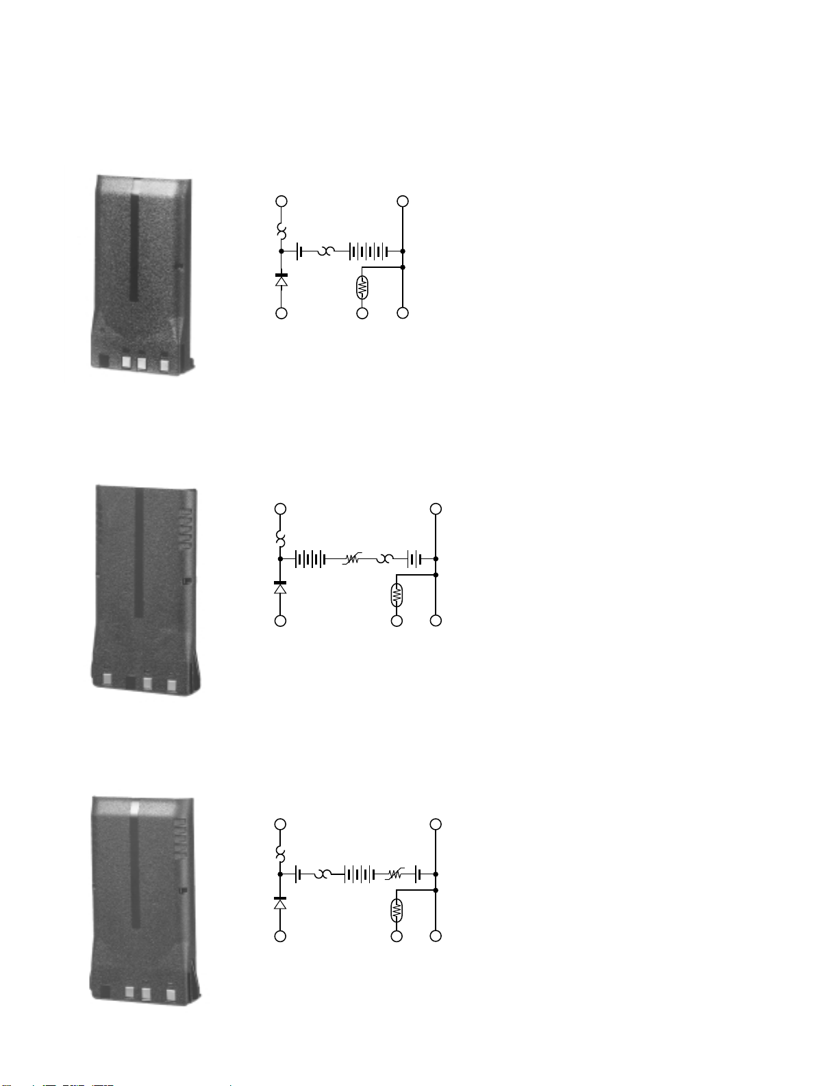
TK-5400
KNB-17A (Ni-Cd Battery) / KNB-21N/22N (Ni-MH Battery)
KNB-17A
External View
KNB-21N
External View
KNB-17A
Schematic Diagram
Discharge pin side
+
Breaker
(70±5°C)
Diode
Breaker
(80±5°C)
Thermister
+
Charge pin side
T
KNB-21N
Schematic Diagram
Discharge pin side
+
Breaker
(70°C)
Poly switch
Diode
+
Charge pin side
Breaker
Thermister
(80°C)
KNB-17A
Specifications
–
–
Voltage .............................................. 7.2V (1.2V x 6)
Charging current ....................................... 1500mAh
Dimensions (mm) .......... 58.0 W x 110.8 H x 20.0 D
(Projections included)
Charger and charging time
KSC-19 (Normal Charger) ............ Approx. 8 hours
KSC-20 (Rapid charger) .............. Approx. 1.3 hour
Weight .............................................................. 220g
KNB-21N
Specifications
–
–
T
Voltage .............................................. 7.2V (1.2V x 6)
Charging current ....................................... 1600mAh
Dimensions (mm) .......... 63.8 W x 110.8 H x 17.2 D
(Projections included)
Charger and charging time
KSC-24 (Rapid charger) ......... Approx. 80 minutes
Weight .............................................................. 210g
KNB-22N
External View
KNB-22N
Schematic Diagram
Discharge pin side
+
Breaker
(70°C)
Diode
Breaker
+
(80°C)
Charge pin side
Poly switch
Thermister
KNB-22N
Specifications
Voltage .............................................. 7.2V (1.2V x 6)
–
–
T
Charging current ....................................... 2100mAh
Dimensions (mm) .......... 63.8 W x 110.8 H x 20.2 D
(Projections included)
Charger and charging time
KSC-24 (Rapid charger) ....... Approx. 110 minutes
Weight .............................................................. 250g
63

TK-5400
KSC-19 (Regular Charger) / KSC-20/24 (Rapid Charger)
KPG-36 (Programming Interface Cable) /
KPG-36 External View
KSC-19 External View
KSC-20 External View
KSC-20 Specifications
Charging current ..................... 1100mA±150mA
Charging time ......................... KNB-17A : Approx. 80 min.
Source voltage ........................ Approx. 15V
Usable temperature range ...... 0°C~40°C
Dimensions (Body only) .......... 105 W x 52 H x 135 D (mm)
Weight (Body only) ................. 0.18kg
KSC-24 External View
KSC-19 Charging
KNB-17A
Voltage ................................................. 7.2V
Battery capacity ................................... 1500mAh
Charging time ....................................... Approx. 8 hours
64
KSC-24 Specifications
Charging current ..................... 1100mA±150mA
Charging time ......................... KNB-17A : Approx. 80 min.
KNB-21N : Approx. 80 min.
KNB-22N : Approx. 110 min.
Source voltage ........................ Approx. 15V
Usable temperature range ...... 0°C~40°C
Dimensions (Body only) .......... 105 W x 55 H x 135 D (mm)
Weight (Body only) ................. Approx. 180g

TK-5400
SPECIFICATIONS
GENERAL
Frequency Range ............................................................. 806 to 825MHz, 851 to 870MHz : TX 851 to 870MHz : RX
Number of Channels ........................................................ 512 channels
Zones ............................................................................... 16 max.
Channels .......................................................................... 250 max.
Channel Spacing .............................................................. FM analog : 12.5/25kHz (NPSPAC) Digital (C4FM) : 12.5kHz
Operating Voltage ............................................................ 7.5V DC ± 20%
Battery Life (5-5-90 duty cycle) ....................................... KNB-17A (Ni-Cd) : 7 hours
KNB-21N (Ni-MH) : 8 hours
KNB-22N (Ni-MH) : 10 hours
Operating Temperature Range ........................................ –22°F to +140°F (–30°C to +60°C)
Frequency Stability (–22°F to +140°F) ............................ ±1.5ppm
Antenna Impedance ........................................................ 50Ω
Dimensions (W x H x D) (Projections not included) ........ 2-5/16 x 6-3/32 x 1-1/2 in. (58 x 155 x 38 m) with KNB-17A battery
Weight (net) ..................................................................... 1.29 lbs (587g) with KNB-17A (no antenna)
RECEIVER
Sensitivity ........................................................................ Digital C4FM @5% BER : 0.30µV FM 12dB SINAD : 0.30µV
Selectivity ........................................................................ Digital : 60dB FM @25kHz : 72dB FM @12.5kHz : 63dB
Intermodulation Distortion ............................................... Digital : 70dB FM @25kHz : 70dB FM @12.5kHz : 63dB
Spurious and Image ......................................................... Digital : 73dB FM : 73dB
Audio Output (into 16Ω) .................................................. 500mW
Audio Distortion ............................................................... Less than 3%
TRANSMITTER
RF Power Output ............................................................. Hi : 3W, Low : 1W
Spurious and Harmonics.................................................. 60dB
FM Hum and Noise ......................................................... FM @25kHz : 45dB FM @12.5kHz : 39dB
Audio Distortion ............................................................... Less than 2%
Modulation ....................................................................... 16K0F3E, 11K0F3E, 8K10F1E, 8K10F1D
FM measurements made per TIA/EIA 603.
Digital measurements made per TIA/EIA 102.
KENWOOD reserves the right to change specifications without prior notice.
APPLICABLE MIL-STD
Standard MIL 810C MIL 810D 810E 810F
Methods/Procedures Methods/Procedures Methods/Procedures Methods/Procedures
Low Pressure 500.1/Procedure I 500.2/Procedure I, II 500.3/Procedure I, II 500.4/Procedure I, II
High temperature 501.1/Procedure I, II 501.2/Procedure I, II Cat. A1 501.3/Procedure I, II Cat. A1 501.4/Procedure I, II
Low temperature 502.1/Procedure I 502.2/Procedure I, II Cat. C1 501.3/Procedure I, II Cat. C1 502.4/Procedure I, II
Temperature Shock 503.1/Procedure I 503.2/Procedure I Cat. A1, C1 503.3/Procedure I Cat. A1, C1 503.4/Procedure I, II
Solar Radiation 505.1/Procedure I 505.2/Procedure I 505.3/Procedure I 505.4/Procedure I
Rain 506.1/Procedure I, II 506.2/Procedure I, II 506.3/Procedure I, II 506.4/Procedure I, III
Humidity 507.1/Procedure II 507.2/Procedure II 507.3/Procedure II 507.4
Salt Fog 509.1/Procedure I 509.2/Procedure I 509.3/Procedure I 509.4
Dust 510.1/Procedure I 510.2/Procedure I 510.3/Procedure I 510.4/Procedure I, III
Vibration 514.2/Procedure VIII, X 514.3/Procedure I Cat. 8 514.4/Procedure I Cat. 8 514.5/Procedure I Cat. 20
Shock 516.2/Procedure I, II, V516.3/Procedure I, I
V
516.4/Procedure I, I
V
516.5/Procedure I, IV,
V
65

TK-5400
KENWOOD CORPORATION
14-6, Dogenzaka 1-chome, Shibuya-ku, Tokyo 150-8501, Japan
KENWOOD SERVICE CORPORATION
P.O. BOX 22745, 2201 East Dominguez Street, Long Beach, CA 90801-5745, U.S.A.
KENWOOD ELECTRONICS CANADA INC.
6070 Kestrel Road, Mississauga, Ontario, Canada L5T 1S8
KENWOOD ELECTRONICS DEUTSCHLAND GMBH
Rembrücker Str. 15, 63150 Heusenstamm, Germany
KENWOOD ELECTRONICS BELGIUM N.V.
Leuvensesteenweg 248 J, 1800 Vilvoorde, Belgium
KENWOOD ELECTRONICS FRANCE S.A.
13, Boulevard Ney, 75018 Paris, France
KENWOOD ELECTRONICS U.K. LIMITED
KENWOOD House, Dwight Road, Watford, Herts., WD1 8EB United Kingdom
KENWOOD ELECTRONICS EUROPE B.V.
Amsterdamseweg 37, 1422 AC Uithoorn, The Netherlands
KENWOOD ELECTRONICS ITALIA S.p.A.
Via G. Sirtori, 7/9 20129 Milano, Italy
KENWOOD IBERICA S.A.
Bolivia, 239-08020 Barcelona, Spain
KENWOOD ELECTRONICS AUSTRALIA PTY. LTD.
(A.C.N. 001 499 074)
16 Giffnock Avenue, Centrecourt Estate, North Ryde, N.S.W. 2113 Australia
KENWOOD ELECTRONICS (HONG KONG) LTD.
Unit 3712-3724, Level 37, Tower one Metroplaza, 223 Hing Fong Road, Kwai Fong, N.T., Hong Kong
KENWOOD ELECTRONICS TECHNOLOGIES(S) PTE LTD.
Sales Marketing Division
1 Ang Mo Kio Street 63, Singapore 569110
 Loading...