


UHF P25 TRANSCEIVER
TK-5310
SERVICE MANUAL
© 2006-12 PRINTED IN JAPAN
B51-8779-00 (S) 570
Helical Antenna
(KRA-23: Option)
Knob (Volume)
(K29-9322-03)
Knob (PTT)
(K29-9328-02)
Main cabinet
(A02-3875-01)
Knob (16CH)
(K29-9323-03)
Helical Antenna
(KRA-23: Option)
Knob (Volume)
(K29-9322-03)
Key top
(EMG)
(K29-9319-03)
Knob (PTT)
(K29-9328-02)
Main cabinet
(4key)
(A02-3877-11)
Knob (16CH)
(K29-9323-03)
Helical Antenna
(KRA-23: Option)
Knob (Volume)
(K29-9322-03)
Key top
(EMG)
(K29-9319-03)
Knob (PTT)
(K29-9328-02)
Key top
(4key)
(K29-9320-03)
Main cabinet
(DTMF)
(A02-3879-11)
Knob (16CH)
(K29-9323-03)
Key top
(EMG)
(K29-9319-03)
Key top
(DTMF)
(K29-9321-13)
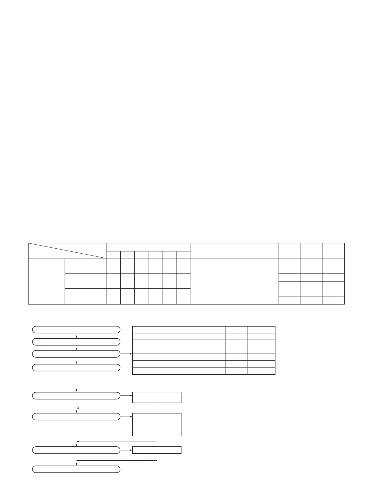
TK-5310 K, K4 TK-5310 K2, K5 TK-5310 K3, K6
Does not come with antenna. Antenna is available as an option.
CONTENTS
GENERAL ............................................................... 2
SYSTEM SET-UP ................................................... 2
REALIGNMENT ...................................................... 3
INSTALLATION .................................................... 10
DISASSEMBLY FOR REPAIR .............................. 11
CIRCUIT DESCRIPTION ....................................... 16
SEMICONDUCTOR DATA ................................... 22
COMPONENTS DESCRIPTION ........................... 24
PARTS LIST .......................................................... 26
EXPLODED VIEW................................................. 39
PACKING .............................................................. 41
ADJUSTMENT ..................................................... 42
TERMINAL FUNCTION ........................................ 62
PC BOARD
TX-RX UNIT (X57-7250-XX) ........................... 66
SCHEMATIC DIAGRAM....................................... 74
INTERCONNECTION DIAGRAM ......................... 86
BLOCK DIAGRAM ................................................ 87
LEVEL DIAGRAM ................................................. 90
SPECIFICATIONS .............................. BACK COVER
TK-5310
GENERAL / SYSTEM SET-UP
Document Copyrights
Copyright 2006 by Kenwood Corporation. All rights
reserved.
No part of this manual may be reproduced, translated,
distributed, or transmitted in any form or by any means,
electronic, mechanical, photocopying, recording, or otherwise, for any purpose without the prior written permission
of Kenwood.
Disclaimer
While every precaution has been taken in the preparation
of this manual, Kenwood assumes no responsibility for
errors or omissions. Neither is any liability assumed for damages resulting from the use of the information contained
herein. Kenwood reserves the right to make changes to any
products herein at any time for improvement purposes.
INTRODUCTION
SCOPE OF THIS MANUAL
This manual is intended for use by experienced technicians
familiar with similar types of commercial grade communications
equipment. It contains all required service information for the
equipment and is current as of the publication date. Changes
which may occur after publication are covered by either Service
Bulletins or Manual Revisions. These are issued as required.
ORDERING REPLACEMENT PARTS
When ordering replacement parts or equipment information, the
full part identification number should be included. This applies to all
parts : components, kits, or chassis. If the part number is not known,
include the chassis or kit number of which it is a part, and a sufficient
description of the required component for proper identification.
PERSONAL SAFETY
The following precautions are recommended for personal safety:
• DO NOT transmit until all RF connectors are verified se-
cure and any open connectors are properly terminated.
•SHUT OFF and DO NOT operate this equipment near elec-
trical blasting caps or in an explosive atmosphere.
•
This equipment should be serviced by a qualified technician only.
SERVICE
This transceiver is designed for easy servicing. Refer to
the schematic diagrams, printed circuit board views, and
alignment procedures contained within.
NOTE
You must use KPG-95D version 5.00 or later for this trans-
ceiver. KPG-95D versions earlier than version 5.00 will not
work properly.
Model &
Unit X57-725X-XX
Destination (Market code)
K ✓
K2 ✓ 450~520 MHz ✓✓
TK-5310
K3 ✓ 1st IF:49.95MHz ✓✓✓
K4 ✓ LOC:50.4MHz
K5 ✓ 380~470 MHz ✓✓
K6 ✓✓✓✓
SYSTEM SET-UP
Merchandise received
License and frequency allocated by FCC
Choose the type of transceiver
Transceiver programming
Are you using the optional antenna?
NO
Are you using the speaker microphone?
NO
Are you using the voice guide & storage unit?
NO
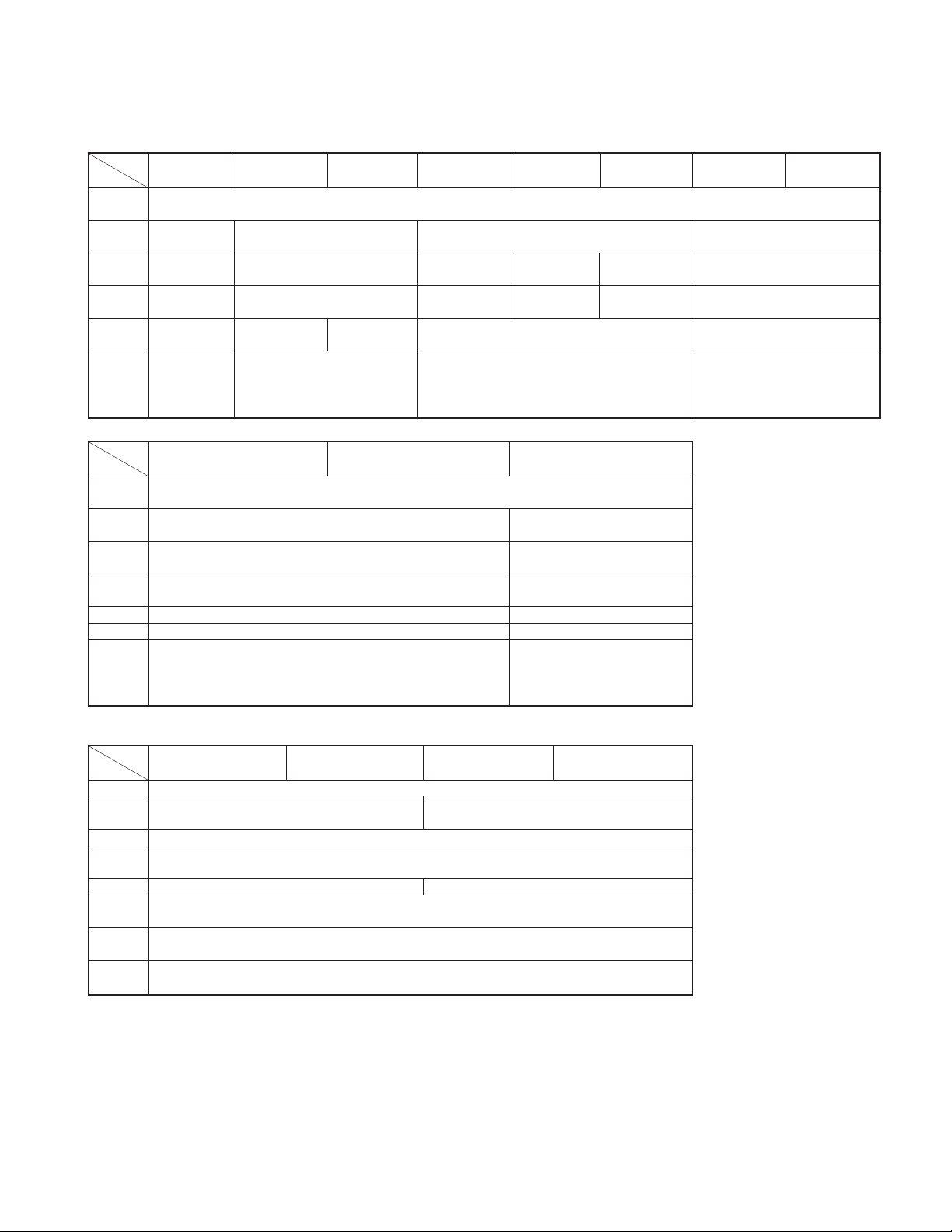
0-10 0-11 0-12 0-13 0-14 0-15
Frequency range (MHz) RF power Type LCD 4-key
TX/RX 450~520 4W TK-5310 K No No No
TX/RX 450~520 4W TK-5310 K2 Yes Yes
TX/RX 450~520 4W TK-5310 K3 Yes Yes Yes
TX/RX 380~470 4W TK-5310 K4 No No
TX/RX 380~470 4W TK-5310 K5 Yes Yes No
TX/RX 380~470 4W TK-5310 K6 Yes Yes
A personal computer (IBM PC or compatible), programming interface (KPG-36/36A), USB
adapter(KCT-53U), and programming software (KPG-95D) are required for programming.
(The frequency, and signaling data are programmed for the transceiver.)
YES
YES
YES
KRA-23 or KRA-27
Helical antenna
(Option)
KMC-25
Speaker microphone
or
KMC-38GPS
GPS speaker microphone
(Option)
VGS-1
(Option)
Frequency range
See page 10
Remarks LCD 4-key
DTMF keypad
DTMF
keypad
---
-
---
-
No
No
Yes
2
Delivery
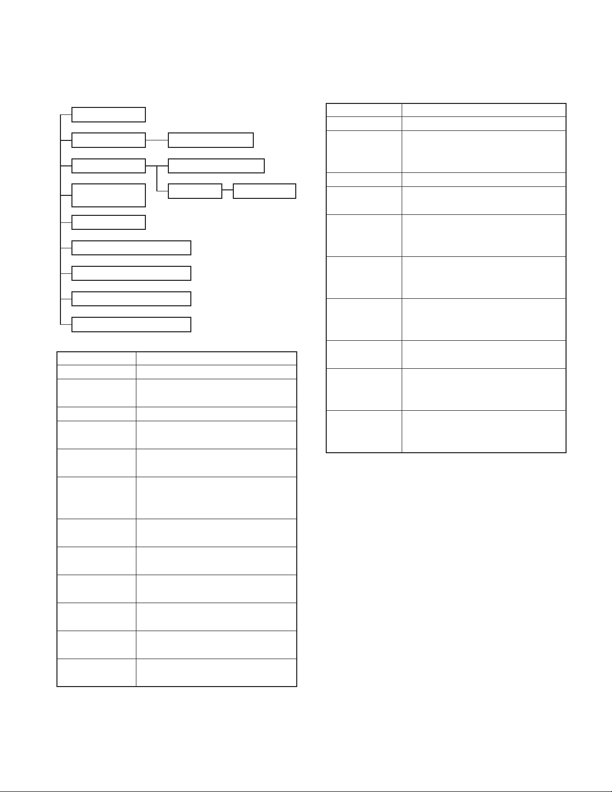
TK-5310
REALIGNMENT
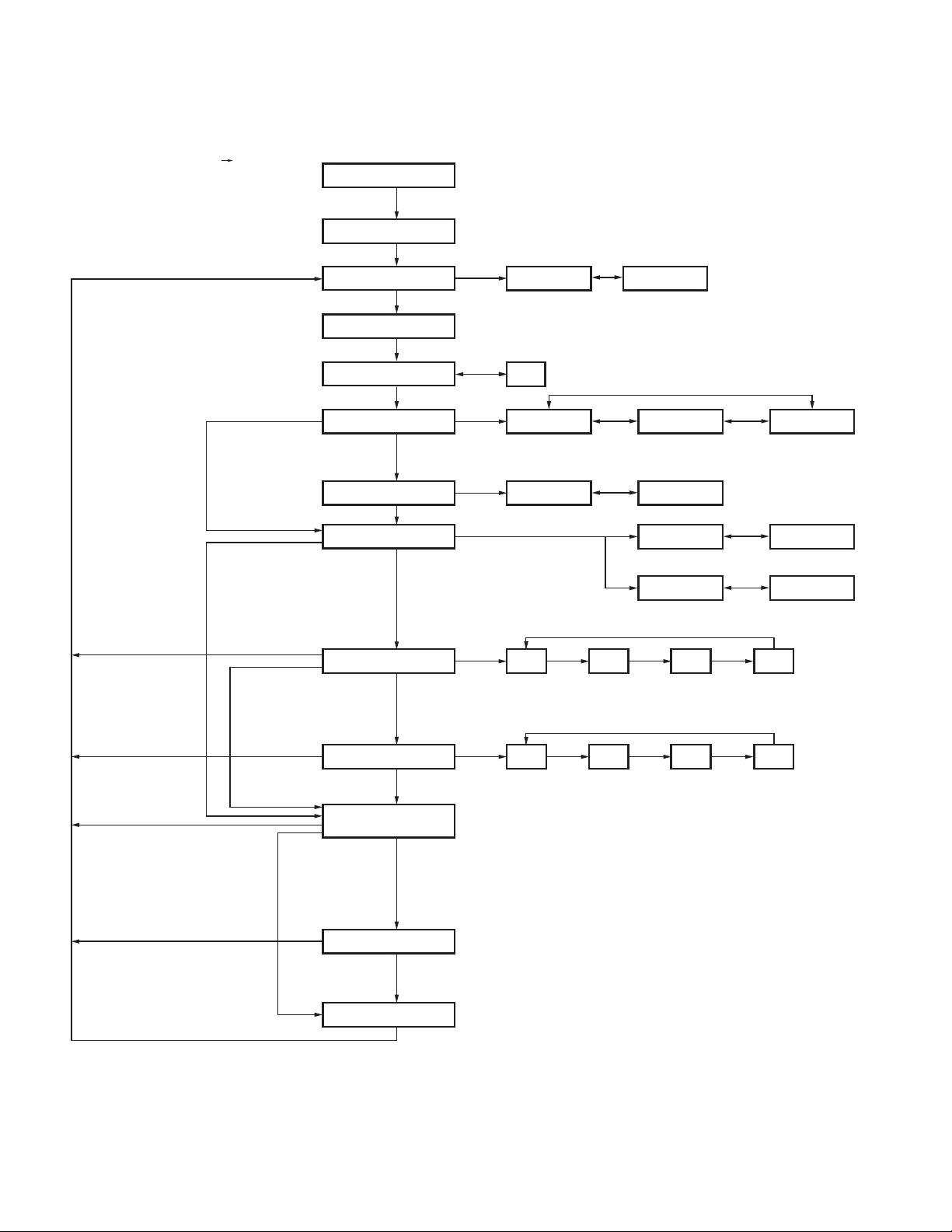
1. Modes 2. How to Enter Each Mode
User mode
Panel test mode
PC mode
Firmware
programming mode
Clone mode ∗1
Self programming mode
Firmware version information
Clock adjustment mode ∗1
Transceiver information mode ∗1
Mode Function
User mode For normal use.
Panel test mode ∗1 Used by the dealer to check the fundamen-
Panel tuning mode ∗1
PC mode Used for communication between the
Data programming Used to read and write frequency data and
mode other features to and from the transceiver.
PC test mode Used to check the transceiver using the PC.
Firmware Used when changing the main program of
programming mode the flash memory.
Clone mode ∗1 Used to transfer programming data from
Self programming Frequency, signaling and features write to
mode ∗1 the transceiver.
Firmware version Used to confirm the internal firmware
information ∗1 version.
Clock adjustment Used by the dealer to adjust date and time.
mode ∗1
Transceiver Used to confirm the transceiver firmware
information mode ∗1 version.
∗
1 : K2, K3, K5 and K6 models only
∗
1
tal characteristics.
Used by the dealer to tune the transceiver.
transceiver and PC (IBM compatible).
This feature is included in the FPU.
See panel tuning.
one transceiver to another.
Panel tuning mode ∗1
Data programming mode
PC test mode
∗
1
∗
1
PC tuning mode
Mode Operation
User mode Power ON
Panel test mode ∗2 Press and hold the [Side3] and [PTT] keys
while turning the transceiver power ON and
then release the [PTT] key first.
PC mode Received commands from PC
Panel tuning Press the [Side3] key, in Panel test mode
mode ∗2
Firmware
programming mode
Clone mode ∗2 Press and hold the [Side2] and [PTT] keys
Self
programming
mode ∗2 while turning the transceiver power ON and
Firmware version
information ∗2 the transceiver power ON.
Clock adjustment Press and hold the [Orange] and [PTT] keys
mode ∗2 while turning the transceiver power ON and
Transceiver Press and hold the [Side1] and [PTT] keys
information mode ∗2
∗
2 : K2, K3, K5 and K6 models only
Press and hold the [Side3] and [PTT] keys
while turning the transceiver power ON and
then release the [Side3] key first.
while turning the transceiver power ON and
then release the [Side2] key first.
Press and hold the [Side2] and [PTT] keys
then release the [PTT] key first.
Press and hold the [Side3] key while turning
then release the [Orange] key first.
while turning the transceiver power ON and
then release the [PTT] key first.
3. Panel Test Mode
(K2, K3, K5 and K6 models only)
Setting method refer to ADJUSTMENT.
4. Panel Tuning Mode
(K2, K3, K5 and K6 models only)
Setting method refer to ADJUSTMENT.
3
TK-5310
REALIGNMENT
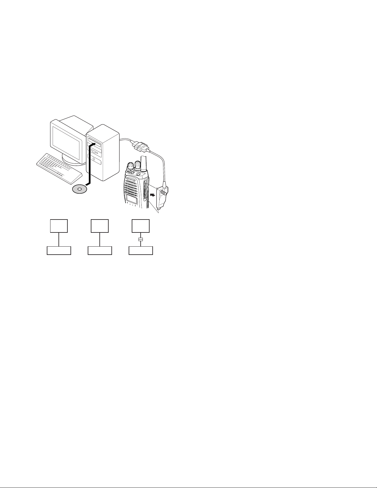
5. PC Mode
5-1. Preface
The transceiver is programmed by using a personal computer, programming interface (KPG-36/36A), USB adapter
(KCT-53U) and programming software (KPG-95D).
The programming software can be used with an IBM PC
or compatible. Figure 1 shows the setup of an IBM PC for
programming.
IBM-PC
KPG-95D
PC
D-SUB
(25-pin)
KPG-36
Tra nsceiver
PC
D-SUB
(9-pin)
KPG-36A
Tra nsceiver
Fig. 1
5-2. Connection procedure
1. Connect the transceiver to the computer using the inter-
face cable and USB adapter (When the interface cable is
KPG-36A, the KCT-53U can be used.).
Notes:
•
You must install the KCT-53U driver in the computer to use
the USB adapter (KCT-53U).
•
When using the USB adapter (KCT-53U) for the first time,
plug the KCT-53U into a USB port on the computer with
the computer power ON.
2.
When the POWER switch on, user mode can be entered
immediately. When PC sends command the transceiver
enter PC mode, and “PROGRAM” is displayed on the LCD.
When data transmitting from transceiver, the red LED is lights.
When data receiving to transceiver, the green LED is lights.
Notes:
•
The text message are displayed for K2, K3, K5 and K6 mod-
els only.
• The data stored in the computer must match the "Model
Name and Market Code" when it is written into the
EEPROM and flash memory.
4
KPG-36 or KPG-36A or
KPG-36A + KCT-53U
Illustration is KPG-36.
PC
USB
KCT-53U
KPG-36A
Transceiver
5-3. KPG-36/KPG-36A description
(PC programming interface cable: Option)
The KPG-36/36A is required to interface the transceiver to
the computer. It has a circuit in its D-sub connector (KPG-36
: 25-pin, KPG-36A : 9-pin) case that converts the RS-232C
logic level to the TTL level.
The KPG-36/36A connects the universal connector of the
transceiver to the RS-232C serial port of the computer.
5-4. KCT-53U description (USB adapter : Option)
The KCT-53U is a cable which connects the KPG-36A to a
USB port on a computer.
When using the KCT-53U, install the supplied CD-ROM
(with driver software) in the computer. The KCT-53U driver
runs under Windows 2000 or XP.
5-5. Programming software KPG-95D description
The KPG-95D is the programming software for the transceiver supplied on a CD-ROM. This software runs under MSWindows 98, ME, Windows 2000 or XP on an IBM-PC or
compatible machine.
The data can be input to or read from the transceiver and
edited on the screen. The programmed or edited data can be
printed out. It is also possible to tune the transceiver.
6. Firmware Programming Mode
6-1. Preface
Flash memory is mounted on the transceiver. This allows
the transceiver to be upgraded when new features are released in the future. (For details on how to obtain the firmware, contact Customer Service.)
6-2. Connection procedure
Connect the transceiver to the personal computer (IBM
PC or compatible) using the interface cable (KPG-36/36A) and
USB adapter (KCT-53U : when the interface cable is KPG36A, the KCT-53U can be used.). (Connection is the same as
in the PC Mode.)
6-3. Programming
1. Start up the firmware programming software (Fpro.exe).
2. Set the communications speed (normally, 115200 bps)
and communications port in the configuration item.
3. Set the firmware to be updated by File name item.
4. Press and hold the [Side3] and [PTT] keys while turning
the transceiver power ON and then release the [Side3] key
first. Then, the orange LED on the transceiver lights and
the baud rate is displayed as follows according to the posi-
tion of the Concentric switch.
A: PROGRAM 115200 bps
B: PROGRAM 57600 bps
C: PROGRAM 19200 bps
Since the baud rate is normally set to 115200 bps, change
the Concentric switch to "A".
5. Check the connection between the transceiver and the
personal computer, and make sure that the transceiver is
in the Program mode.
6. Press “write” button in the window. When the transceiver starts to receive data, the [PG] display lights.

REALIGNMENT
TK-5310
7. If writing ends successfully, the checksum is calculated
and a result is displayed.
8. If you want to continue programming other transceivers,
repeat steps 4 to 7.
Notes:
• This mode cannot be entered if the Firmware Programming mode is set to Disable in the Programming software.
• The text message are displayed for K2, K3, K5 and K6
models only.
These transeivers use firmware versions F4.00 or later.
•
When using firmware versions earlier than version F4.00, a
“Check connection” error message will appear on the
LCD. Firmware versions earlier than version F4.00 will not
write to the transceiver.
6-4. Baud rate change
1. Change baud rate by changing the Concentric switch position. The baud rates are assigned to positions of the Concentric switch as follows:
A: PROGRAM 115200 bps (The LED lights orange)
B: PROGRAM 57600 bps (The LED blinks orange)
C: PROGRAM 19200 bps (The LED blinks green)
2. If you press the [Side1] switch (top of left side) while the
baud rate (such as “PROGRAM 115200 bps") is displayed,
the checksum is calculated, and a result is displayed. If
you press the [Side1] switch again while the checksum is
displayed, the baud rate (such as “PROGRAM 115200
bps") is redisplayed.
Notes:
• Normally, write in the high-speed mode.
• The text message are displayed for K2, K3, K5 and K6
models only.
7. Clone Mode (K2, K3, K5 and K6 models only)
Programming data can be transferred from one transceiver
to another by connecting them via their external universal connectors. The operation is as follows (the transmit transceiver
is the source and the receive transceiver is a target).
The following data cannot be cloned.
• Tuning data
• Embedded message with password
• Model name data
• ESN (Electronic Serial Number) data
• Network file data (P25)
Key guide on the "INPUT PASSWORD" display.
• CNF([A] key): The password confirmation
• DEL([B] key): Delete the least digit from the current pass-
word number (Press and hold to delete all
password numbers)
• SET([D] key):
Determine the least digit of the password number
3.
• How to enter the password using the keypad (K3 and
K6 models only);
If the [D] key is pressed while "CLONE LOCK" is displayed,
the Read authorization password input screen (INPUT
PASSWORD) is displayed.
If one of keys 0 to 9 is pressed while "INPUT PASSWORD"
is displayed, the pressed number is displayed on the LCD.
Each press of the key shifts the display in order to the left.
When you enter the password and press the [A] or [✳]
key, “CLONE MODE” is displayed if the entered password is correct. If the password is incorrect, “CLONE
LOCK” is redisplayed.
• How to enter the password using the [Side2] and
[Side3] keys (K2, K3, K5 and K6 models);
If the [D] key is pressed while "CLONE LOCK" is displayed,
the Read authorization password input screen (INPUT
PASSWORD) is displayed.
If the [Side2] key or [Side3] key is pressed while "INPUT
PASSWORD" is displayed, the number (0 to 9) flashes on
the LCD. When you press the [D] key, the currently
selected number is determined. If you press the [A] key
after entering the password in this procedure, “CLONE
MODE” is displayed if the entered password is correct. If
the password is incorrect, “CLONE LOCK” is redisplayed.
4. Power ON the target transceiver.
5. Connect the cloning cable (part No. E30-3325-05) to the
universal connectors on the source and target.
6. Press the [Side1] or [A] key on the source while the source
displays “CLONE MODE”. The data of the source is sent
to the target. While the target is receiving the data, “PROGRAM” is displayed. When cloning of data is completed,
the source displays “END”, and the target automatically
operates in the User mode. The target can then be operated by the same program as the source.
7. The other target can be continuously cloned. When the
[Side1] or [A] key on the source is pressed while the
source displays “END”, the source displays “CLONE
MODE”. Carry out the operation in step 4 to 6.
Notes:
• Cannot be cloned if the password (overwrite password) is
programmed to the target.
•
Cannot be cloned if the checksum in the Network File area of
the source transceiver and the target transceiver is different.
•"Model Name and Market Code" must be same to clone
the transceiver. However, it may be unable to clone the
transceiver depending on the enhanced features settings.
(Refer to the FPU for the enhanced features details.)
• Under certain conditions, clone mode cannot be activated
even if the clone mode of the source transceiver is set to
enable. Refer to the FPU for more details.
Cloning cable
(E30-3325-05)
1.
Press and hold the [Side2] and [PTT] keys while turning the
transceiver power ON and then release the [Side2] key first.
If the Read authorization password is set to the transceiver,
the transceiver displays “CLONE LOCK”. If the password is
not set, the transceiver displays “CLONE MODE”.
2.
When you enter the correct password, and “CLONE MODE”
is displayed, the transceiver can be used as the cloning
source. The following describes how to enter the password.
Fig. 2
5
TK-5310
REALIGNMENT
8. Self Programming Mode
(K2, K3, K5 and K6 models only)
Write mode for frequency data and signaling etc. To be
used ONLY by the authorized service person maintaining the
user's equipment. After programming, reset the FPU to the
"Self- Programming" disabled mode. Transceivers CANNOT
be delivered to the end-user in the self-programming mode.
The following setup items in the channels programmed by
the FPU can be changed using the self-programming mode.
The addition of new channel and the deletion of channel that
has already been programmed by the FPU cannot be
performed using the self-programming mode.
• RX frequency
• TX frequency
• Channel type
• TX mode (When the channel type is selected "MIXED".)
• Channel spacing
• RX signaling
• TX signaling
• RX NAC
• TX NAC
• Talkgroup list number
Note:
The personality will be also changed when the above-
mentioned items is changed. (Refer to the FPU for the
personality details.)
8-1. Enter to the self programming mode
Press and hold the [Side2] and [PTT] keys while turning
the transceiver power ON and then release the [PTT] key
first. Ignoring whether the Read authorization password is
set or not, "INPUT PASSWORD" appears.
If the Read authorization password is not set to the transceiver, "SELF PROG MODE" is displayed on the LCD when the
[A] key is pressed while "INPUT PASSWORD" is displayed.
If the password is set to the transceiver, "SELF PROG
MODE" is displayed on the LCD when you enter the correct
password while "INPUT PASSWORD" is displayed.
For the password input method, see "7.Clone Mode”
step 3 described on page 5.
Note :
This mode (self programming mode) cannot be set when
it has been disabled with the FPU.
8-2. Data Writing
If the [Side3] key is pressed while Zone/Channel mode is
displayed, new data is written into memory. "Writing" is displayed while the transceiver is writing data.
Key guide on the "INPUT PASSWORD" display.
• CNF([A] key): The password confirmation
• DEL([B] key): Delete the least digit from the current password number (Press and hold to delete all
• SET([D] key): Determine the least digit of the password
password numbers)
number
The setup items for self programming mode are as follows.
No. Setup item Display Remarks
1 Select ZONE [**] -CH *** Zone : 1~50
Zone/Channel ZONE ** -CH [***] CH : 1~250
2 RX frequency RX Freq Receive frequency
3 TX frequency TX Freq Transmit frequency
4 Channel type CH Type ANALOG/P25/MIXED
5 TX mode TX Mode ANALOG/P25
6Channel spacing CH Space 25.0kHz/12.5kHz
P25 12.5kHz/12.5kHz (When the Channel type is selected "P25".)
7 RX Signaling RX Sig Receive QT/DQT
8 TX Signaling TX Sig Transmit QT/DQT
9 RX NAC RX NAC *** 000~FFF (Hexadecimal) Note : “F7F” cannot be set.
10 TX NAC TX NAC *** 000~FFF (Hexadecimal) Note : “F7E” and “F7F” cannot be set.
11 Talkgroup list number TG List No. *** 1~250
(When the Channel type is selected "ANALOG" or "MIXED".)
6
TK-5310
REALIGNMENT
Key operation
Item
Key
[Side3]
Keypad
[0]~[9]
(K3 and K6 (After selecting signaling type)
models only)
Zone-Channel RX Frequency TX Frequency Channel Type TX Mode Channel Spacing RX Signaling TX Signaling
[A] Go to the next item
Zone/ Channel 5kHz/6.25kHz/1MHz
[B]
[C]
[D]
switching step switching switching
Zone/ Channel
down switching(Back) switching(Back) switching(Back)
Zone/ Channel
up
Data
writing switching switching
Unused Go to the direct enter mode Unused
Unused
1 step down
1 step up
ON/OFF
Unused
ANALOG/P25/MIXED
ANALOG/P25/MIXED
switching(Forward) switching(Forward) switching(Forward)
ANALOG/P25 Channel spacing
ANALOG/P25 Channel spacing
Unused
QT/DQT(N)/DQT(I)/OFF
Signaling down
Signaling up
1 step/Standard
Go to the direct enter mode
Item
Key
[A] Go to the next item
[B]
[C] Unused
[D] Determine the least digit
[Side2] Increment a number in the specified digit Unused
[Side3] Decrement a number in the specified digit Unused
Keypad Add a digit to the current number
(K3 and K6 How to enter the “A” ~ “F” is follows.
models only)
A : Press [2] with PTT B : Press [5] with PTT C : Press [8] with PTT
D : Press [0] with PTT E : Press [#] with PTT F : Press [*] with PTT
RX NAC TX NAC TG List No.
Delete the least digit from the current number
(Press and hold to delete all numbers.)
number down
number up
• Direct enter mode
Item
Key
[A] Return to non-direct enter mode
[B] Unused
[C] Unused
[D]
[Side3] ON/OFF switching at TX Frequency Unused
Keypad
[0] ~ [9]
Keypad
[*]
Keypad Delete the least digit from the current number
[#] (Press and hold to delete all numbers.)
RX Frequency TX Frequency RX Signaling TX Signaling
Change the type of signaling and
return to non-direct enter mode
Delete the least digit from the current number
(Press and hold to delete all numbers.)
Add a digit to the current number
Return to non-direct enter mode
Unused
TG List
TG List
Unused
7
TK-5310
●
Self programming mode flow chart
[Side2] + [PTT] + POWER ON Release [PTT]
REALIGNMENT
Input Password
Read authorization password entry (6 digits)
[A]
Self programming mode
[A]
Zone/Channel
[A] When the [Side3] key is pressed, new data is written into memory.
RX frequency
[A]
Zone selection
[B]
Channel selection
[A] [A]
[TX frequency] : "OFF"
[Channel type] : "ANALOG" or "P25"
[A]
[Channel type] : "P25"
[A]
[TX frequency] : "OFF"
[Channel type] : "ANALOG"
[A]
[Channel type] : "ANALOG"
[A]
[TX frequency] : "OFF"
Talkgroup ID List Amount : 0
or
[TX frequency] : Other than "OFF"
[Channel type] : "MIXED"
[TX mode] : "ANALOG"
Talkgroup ID List Amount : 0
[A]
Talkgroup ID List Amount : 0
TX frequency
Channel type
TX mode
Channel spacing
RX signaling
[A]
[TX frequency] : "OFF"
[Channel type] : "P25" or "MIXED"
TX signaling
[A]
[TX frequency] : "OFF"
Talkgroup list number
RX NAC
TX NAC
[Side 3]
[A]
[TX frequency] : Other than "OFF"
[Channel type] : "MIXED"
[A]
[A]
[Channel type] : "ANALOG" or "MIXED"
[A]
[TX frequency] : Other than "OFF"
[Channel type] : "ANALOG" or "MIXED"
[TX mode] : "ANALOG"
[A]
[Channel type] : "P25" or "MIXED"
[A]
[TX frequency] : Other than "OFF"
[Channel type] : "P25" or "MIXED"
If [Channel type] is set to "MIXED", [TX mode] must be set to "P25".
[A]
[Channel type] : "P25" or "MIXED"
Talkgroup ID List Amount must not be 0.
[A]
OFF
ANALOG
OFF QT
OFF QT DQT N
[C]/[D]
[C]/[D]
*1
*2
[B] [B] [B]
[B]
[C]/[D]
P25
P25ANALOG
*1 [Channel type] : "ANALOG" or "MIXED"
P25 12.5kHz
*2 [Channel type] : "P25"
[B]
DQT N
[B]
[B]
[C]/[D]
[C]/[D]
[C]/[D]
[B]
MIXED
12.5kHz25.0kHz
12.5kHz
DQT I
DQT I
8
REALIGNMENT
9. Firmware Version Information
(K2, K3, K5 and K6 models only)
Press and hold the [Side3] key while turning the transceiver
power ON and then keep pressing and holding the [Side3] key,
the firmware version information appears on the LCD.
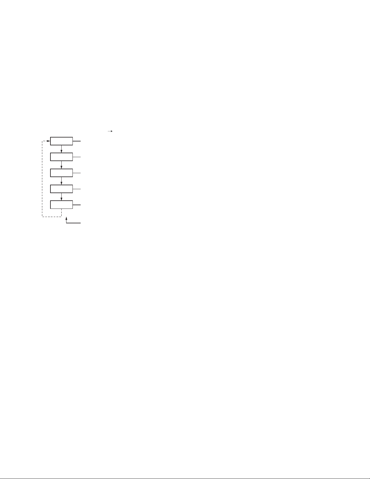
10. Clock Adjustment Mode
(K2, K3, K5 and K6 models only)
10-1. Flow chart of operation
[Orange] + [PTT] + Power ON Release [Orange]
YEAR
[A]
MONTH
[A]
DAY
[A]
HOUR
[A]
MINUTE
[A]
[Side2] and [Side3] keys or [C] and [D] keys
[Side2] and [Side3] keys or [C] and [D] keys
[Side2] and [Side3] keys or [C] and [D] keys
[Side2] and [Side3] keys or [C] and [D] keys
[Side2] and [Side3] keys or [C] and [D] keys
TK-5310
Completion
11. Transceiver Information Mode
(K2, K3, K5 and K6 models only)
Use this function to confirm the transceiver firmware version.
1. Press and hold the [Side1] and [PTT] keys while turning
the transceiver power ON and then release the [PTT] key
first.
2. The transceiver firmware version appears on the LCD.
3. To exit the transceiver information mode, turn the trans-
ceiver power OFF.
9
TK-5310
INSTALLATION
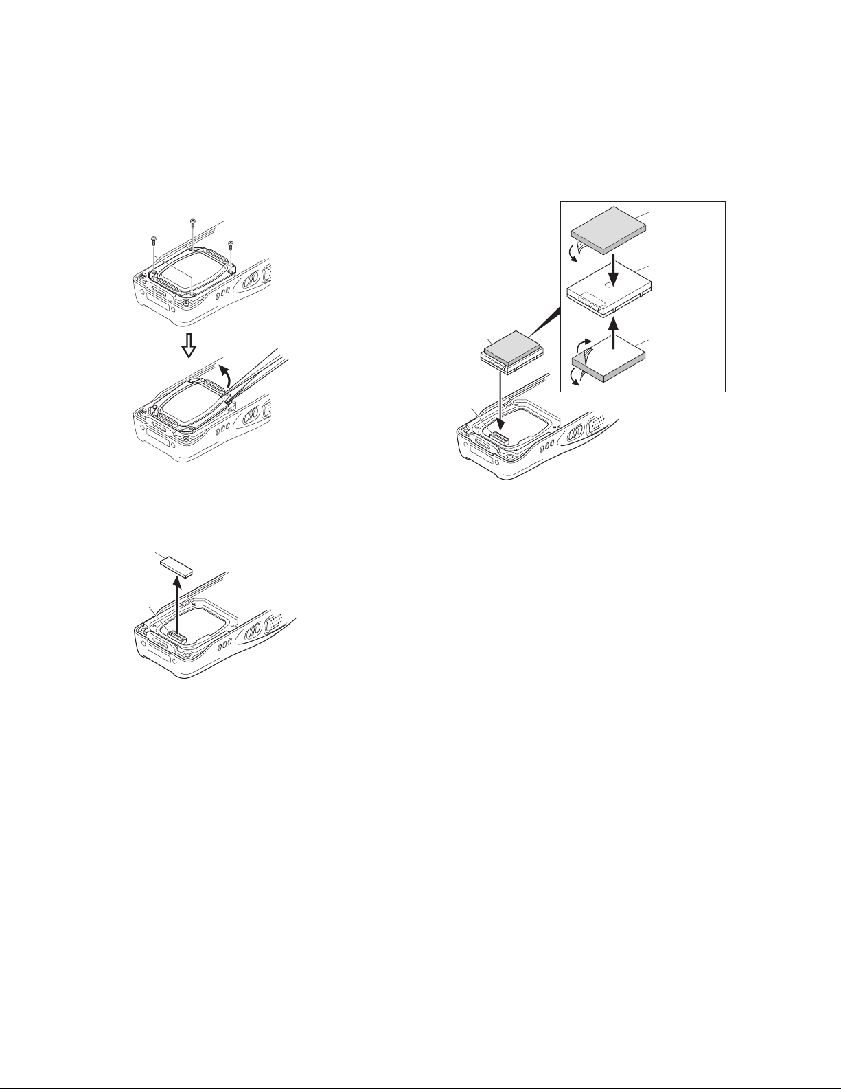
Voice Guide & Storage Unit (VGS-1:Option)
■ Installing the VGS-1 unit in the transceiver
1. Remove the 4 screws from the cover.
2. Remove the cover by inserting the tip of a pair of tweezers
into the screw hole of the cover and prying it open.
5. Insert the VGS-1 connector (CN1) into the connector
(CN609) of the TX-RX PCB.
Cushion
(G13-1995-04)
20X30X1.0mm
VGS-1
Fig. 1
3. Remove the OPTION PCB from the connector (CN609) of
the TX-RX PCB.
OPTION PCB
CN609
Fig. 2
VGS-1
CN1
CN609
Cushion
(G13-1974-04)
21X21X1.0mm
Fig. 3
6. Reinstall the cover using the 4 screws removed in step 1.
Note:
You must setup using the KPG-95D.
Attach two cushions to the VGS-1 as shown in the figure 3.
4.
Note:
Be sure not to cover the VGS-1 connector (CN1) with the
cushion.
10
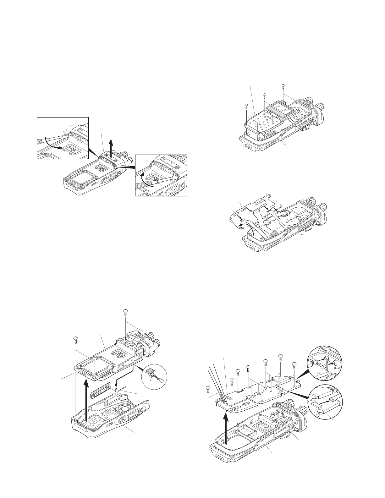
DISASSEMBLY FOR REPAIR
TK-5310
Disassembly Procedure
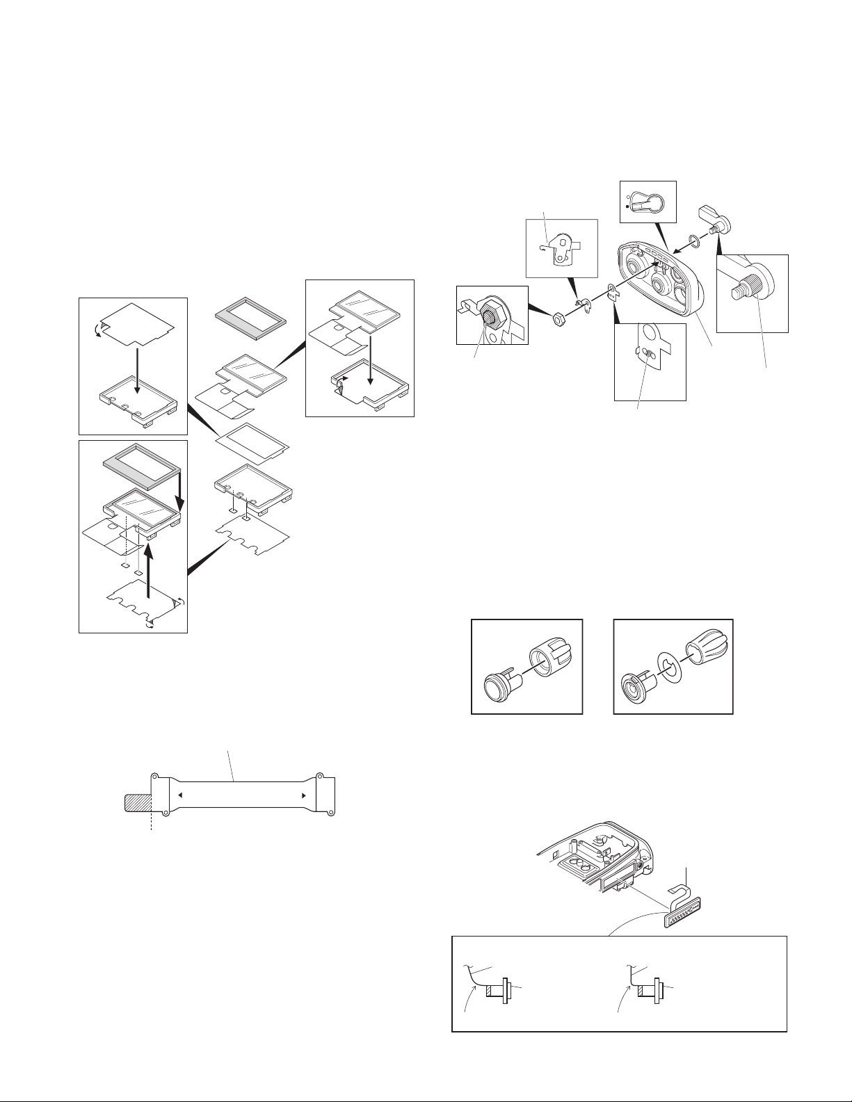
■ Removing the front case from the chassis.
1. Remove the rear panel with a flat-head screwdriver.
Insert the screwdriver between the rear panel (right side)
and the chassis (the place next to the """ mark shown on
the chassis), push it in the direction of the arrow
remove the right side of the rear panel. Repeat the above
action for the left side of the rear panel x.
""" mark
x
2. Remove the four screws c and universal connector cap
Rear panel
z
v.
3. Lift the battery pack release latch on the bottom of the
chassis
Notes:
• Lift the chassis from the front case slowly and carefully. If
the chassis is lifted suddenly, the SP/MIC FPC may be
pulled and the connector may become damaged.
• Handle the main packing with care. It is likely to collect
dust and dirt.
4. Remove the SP/MIC FPC from the CONTROL PCB con-
nector (CN713).
b and remove the chassis from the front case.
n
c
c
Chassis
z, and
""" mark
■ Removing the CONTROL PCB (X57-725 B/5)
from the chassis.
1. Remove the six screws m.
CONTROL PCB
m
m
2. On the reverse side of the CONTROL PCB
cord ASSY and each FPC from the connectors (CN700,
CN800 (K2, K3, K5 and K6 models only), CN803, CN804)
of the CONTROL PCB.
CN803
CN700
CN800
,
m
Chassis
,, remove the
CN804
Cord ASSY
■ Removing the TX-RX PCB (X57-725 A/5) from
the chassis.
1. Remove the 14 screws ..
2. Remove the universal connector FPC from the TX-RX PCB
connector (CN606) /.
3. Insert the two tips of a pair of tweezers into the two holes
in the bottom of the shield plate of the TX-RX PCB, firmly
squeeze the tweezers to hold the shield plate, then
remove the TX-RX PCB
4. Remove the coaxial cables from the two connectors
(MAIN (CN204), UNIV (CN205)) of the TX-RX PCB ≈.
Ω.
Battery pack
release latch
b
v
SP/MIC FPC
Front case
CN713
n
TX-RX PCB
.
Ω
.
.
.
.
Chassis
.
UNIV
(CN205)
.
Universal
connector FPC
≈
/
≈
CN606
MAIN
(CN204)
11
TK-5310
DISASSEMBLY FOR REPAIR
■ Removing the top panel from the chassis.
1. Remove the volume knob ç and channel knob √.
2. Remove the concentric switch knob
3. Remove the volume torque-up packing
tweezers.
4. Remove the nuts from the volume knob, channel knob
and antenna receptacle.
5. Remove the top panel
Notes:
• Before removing the top panel, set the lever switch to the
"-" position (circle painted in white)
• Each of the volume knob, channel knob and antenna receptacle on the top panel has an O-ring. Take care not to
lose them after removing the panel.
µ.
∫.
~ using a pair of
≤.
ç
≤
~
√
∫
µ
O-ring
Precautions for Reassembly
■ Installing the VOL/CH FPC and CONTROL-TOP
FPC on the TOP PCB
1. Remove the volume z and channel switch x from the
chassis.
2. Position the coaxial cable connecting the ANT PCB and
TX-RX PCB as shown in the figure below.
The projection
of the volume
z
CONTROL-TOP
FPC
3. Pass the coaxial cable
through the round hole of the hardware fixture
insert it into the coaxial connector (MAIN (CN204)) of the
TX-RX PCB.
x
VOL/CH FPC
Aline the coaxial cable
connecting the ANT PCB and
TX-RX PCB as shown in the figure.
c of the antenna receptacle
pedestal
The projection of
the channel
switch pedestal
v, then
■ Removing the TOP PCB (X57-725 C/5) from the
chassis.
1. Remove the two screws ≥.
2. Lift the TOP PCB and remove the VOL/CH FPC
CONTROL-TOP FPC
CN903) of the TOP PCB.
21
from the two connectors (CN902,
TOP PCB
CN902
≥
≥
÷ and
÷
21
CN903
v
MAIN
(CN204)
4. Pass the volume, channel switch, VOL/CH FPC and
CONTROL-TOP FPC through hardware fixture holes, then
bring the hardware fixture into contact with the chassis
and fix it with a screw
Note:
The projections of the volume and channel switch pedestals must protrude from the square holes of the hardware
fixture.
5. Fix the antenna receptacle with the two screws n.
6. Fix the hardware fixture with a screw
b.
c
m.
12
b
m
n
DISASSEMBLY FOR REPAIR
tab
CONTROL PCB
TK-5310
7. Insert the VOL/CH FPC , and the CONTROL-TOP FPC .
into the connectors (CN902, CN903) of the TOP PCB.
8. Fix the TOP PCB with a screw
9. Fix the TOP PCB with a screw
CN902
,
/.
Ω.
.
/
Ω
CN903
■ TX-RX PCB Installation Procedure
1. Insert the coaxial cable of the antenna receptacle into the
coaxial connector (CN204) of the TX-RX PCB
coaxial cable of the ANT PCB into the coaxial connector
(CN205) of the TX-RX PCB
2. Grasp both sides of the lower part of the TX-RX PCB, tilt
the TX-RX PCB and install the chassis so that the PTT FPC
x.
z and the
c, CONTROL-TOP FPC v and universal connector FPC
b are not caught n.
3. Fix the TX-RX PCB with the 14 screws.
CN205
c
b
v
n
x
z
CN204
2. Fit the two tabs on the right side of the holder c and the
two tabs on the left side of the holder
CONTROL PCB.
Note:
Take care that the FPC is not caught when fitting the two
tabs on the right side of the holder.
v into the
c
c
v
v
3. Insert the FPC into the CONTROL PCB connector (CN802)
b.
CN802
b
■
Main Packing (G53-1637-04) Installation Procedure
1. Hook the packing (coated with silicon oil) in the upper
groove of the chassis
lower groove of the chassis
Note:
Ensure that the chassis grooves and packing are free from
dirt and dust.
z, then fit the packing into the
x.
Grasp both sides of the lower part
of the TX-RX PCB
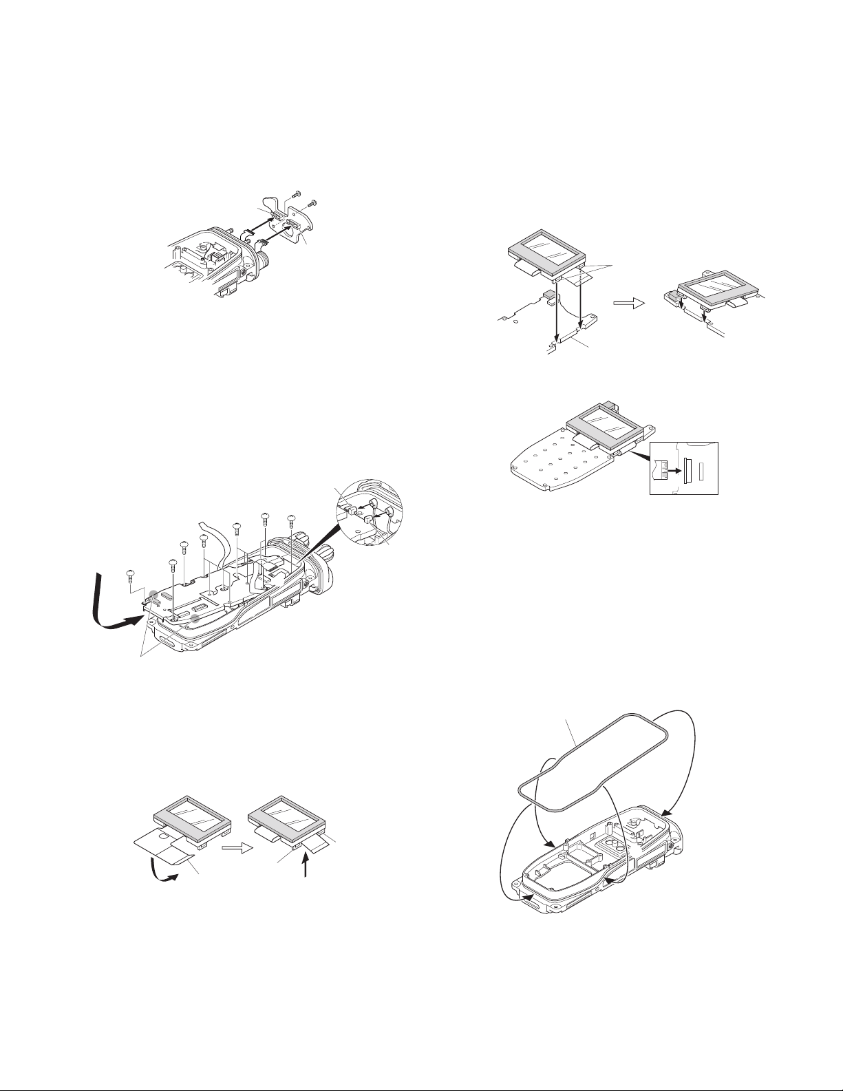
■ LCD ASSY Installation Procedure (K2, K3, K5 and
K6 models only)
1. Fold the LCD ASSY FPC to the back of the holder
that the FPC is between the two tabs on the right side of
the holder x.
tab
x
z
LCD ASSY FPC
z so
tab
2. Fit the packing into the grooves on both sides of the
chassis c. (Fit the packing into the groove in the chassis
by tracing it lightly with your fingers.)
Main packing
z
c
c
x
Note:
To remove the packing from the chassis groove, use a
resin adjustment bar or other such device. If the packing
is pried with a sharp metallic tool, such as tweezers, the
packing may become damaged.
3. Verify that the packing fits snuggly into the groove of the
chassis.
13
TK-5310
DISASSEMBLY FOR REPAIR
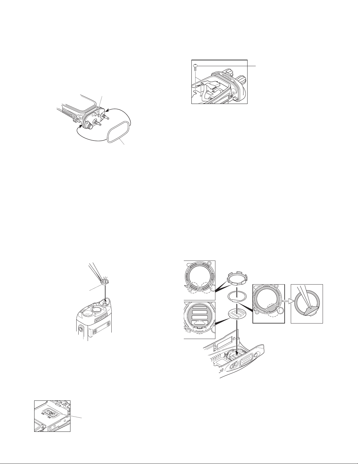
■ Top Packing (G53-1638-04) Installation Procedure
1. Ensure that the hardware fixture is first secured to the
chassis.
2. Hook the packing (coated with silicon oil) in the upper left
groove of the chassis
groove of the chassis.
Notes:
• Verify that the chassis grooves and packing are free from
dirt and dust.
• To remove the packing from the chassis groove, use a
resin adjustment bar or other such device. If the packing
is pried with a sharp metallic tool, such as tweezers, the
packing may become damaged.
3. Verify that the packing fits snuggly into the groove of the
chassis.
z, then fit the packing into the right
x
Hardware fixture
z
x
Top packing
2. Tighten the two screws from the TX-RX PCB side.
Tw o screws
3. Firmly tighten the hexagon screws of the GND terminal.
Installation Procedure during Parts Replacement
■ Attaching the Sheet (G10-1338-04, J99-0383-14)
to the Front Case Speaker and Installation of
the Packing (G53-1633-04)
1. Attach a new fiber sheet z (G10-1338-04) so that its
convex fits the hollow of the front case
2. Attach a new pressure sensitive adhesive sheet
0383-14) so that its convex fits the hollow of the front
case v.
3. Remove the separation sheet from the pressure sensitive
adhesive sheet with a pair of tweezers b.
4. Fit the packing
speaker.
n (G53-1633-04) into the front case
x.
c (J99-
■ Volume Torque-up Packing (G53-1628-04)
Installation Procedure
Insert the packing using a pair of tweezers so that the
hollow of the packing fits the convex of the panel
Volume torque-up packing
z
z.
■ Screw sequence for mounting the battery
terminal block to the chassis.
Attach the battery terminal block to the chassis as
described in the following procedure.
1. Loosely fix the hexagon screws of the GND terminal to
the chassis (enough so that the hexagon screws do not
move).
Note:
Fit the packing into the hollow of the case so that the two
low-height places in the convex of the packing are positioned on the lower side
m.
n
m
c
vb
z
x
5. Verify that the packing does not ride on the rib of the case.
14
GND terminal
■ Installing a new LCD ASSY to the holder (K2,
K3, K5 and K6 models only)
1. Remove the separation paper (brown) from the new sheet
z x, and attach the sheet to the surface of the holder c.
2. Remove the protection sheets attached to both sides of
the new LCD ASSY.
Apply grease to between
the two holes in
the hardware fixture.
Apply bond (Three Bond 1401C)
to the tip of the lever knob shaft
and the surface of the hexagon
nut.
Top panel
Inserted into the hole
on the left side of the
hardware fixture.
Apply grease to the
base of the shaft of
the lever knob.
z
v
m
b
n
x
c
DISASSEMBLY FOR REPAIR
TK-5310
3. Remove the separation paper (white) from the sheet in
v, then attach the LCD ASSY b to the sheet.
step 1
4. Attach two pieces of double-sided adhesive tape
n to the
back of the holder and remove the separation paper.
5. Remove the protection sheet (transparent) attached to
one side of the new filter
sheet (yellow) from the other side
m , and remove the protection
..
6. Attach the filter from step 5 to the back of the holder.
7. Attach the new cushion / so that it fits to the corner of
the holder convex.
/
b
z
x
b
c
v
z
/
c
n
n
n
n
m
,
.
6. Fix the two hardware fixtures with the hexagon nut n.
7. Apply bond (Three Bond 1401C) to the tip of the lever
knob shaft and the surface of the hexagon nut m.
■ Volume Knob and Channel Knob Parts Replacement
Since the volume knob consists of two components, a
knob
z and a spacer x, replace and reinstall these two
parts at the same time.
Since the channel knob consists of three components, a
c, a 16CH display seal v and a spacer b, replace
knob
and reinstall these three parts at the same time.
Volume Knob Channel Knob
■ Preparation when Replacing the Cord ASSY
(X42-3270-10)
Cut the tip of the FPC on the side on which "TX-RX" is
stamped when replacing the cord ASSY.
■ Procedures when Replacing the Top Panel
1. Insert the O-ring z into the lever switch part of the new
top panel.
2. Apply grease to the base of the shaft of the lever knob x
and install the lever knob so that it is in the "-" position
(circle painted in white) on the top panel
3. Pass the hardware fixture
it onto the top panel.
4. Apply grease to between the two holes in the hardware
fixture
5. Install the hardware fixture
hole on the left side of the hardware fixture
CUT
v.
Cord Assy(X42-3270-10)
TX-RX
v through the shaft and install
b so that it is inserted into the
z
x
■
Procedure when replacing the universal connector
b
c
v
FPC (J82-0097-25)
When assembling a new universal connector FPC, insert
CONT
c.
the FPC into the chassis hole by gently bending the FPC
as shown in the figure.
Universal connector FPC
(J82-0097-25)
Right
Universal connector FPC
Universal
Connector
Bend the FPC gently.
Wrong
Universal connector FPC
Universal
Connector
Do not bend the FPC at a sharp angle.
v.
15

TK-5310
CIRCUIT DESCRIPTION
1. Overview
This transceiver is a UHF/FM/P25 portable transceiver
designed to operate in the frequency range of 450 to
520MHz (K, K2, K3) or 380 to 470MHz (K4, K5, K6).
The unit consists of receiver, transmitter, phase-locked
loop (PLL) frequency synthesizer, base band parts, power
supply, and control circuits.
2. Frequency Configuration
The receiver is a double-conversion superheterodyne
using first intermediate frequency (IF) of 49.95MHz and
second IF of 450kHz. Incoming signals from the antenna are
mixed with the local signal from the PLL circuit to produce
the first IF of 49.95MHz.
This is then mixed with the 50.4MHz second local
oscillator output to produce the 450kHz second IF. This
signal is detected to give the demodulated signal in the DSP.
The transmit signal frequency is generated by the PLL
VCO, and modulated by the signal from the DSP. It is then
amplified and fed to the antenna.
ANT
TX/RX : 450~520MHz(K, K2, K3)
TX/RX : 380~470MHz(K4, K5, K6)
1st MIX
SW
PA
RF
AMP
16.8MHz
400.05~470.05MHz(K, K2, K3)
330.05~420.05MHz(K4, K5, K6)
TX
AMP
450~520MHz(K, K2, K3)
380~470MHz(K4, K5, K6)
49.95MHz
VCXO
ANT
AMP
MCF
450kHz
IF AMP
x3
50.4MHz
CF
MIX
PLL
VCO
FPGA
A/D
D/A
DSP
AF
AMP
MIC
AMP
SP
MIC
Fig. 1 Frequency configuration
3. Receiver System
3-1. Front-end RF Amplifier
The signal is passed through an antenna matching coil,
where the high-frequency components are amplified by a
MOS FET(Q301). The signals are then fed into band-pass
filter that uses varactor diode tuning to reject unwanted
signal components, and is fed to the 1st mixer.
3-2. 1st Mixer
The 1st mixer uses the GaAs IC (IC302). The 1st mixer
mixes the signal with the 1st local oscillator frequency from
the VCO, and converts it to the 1st IF (49.95MHz).
The signal then passes through monolithic crystal filter
(XF300) to remove unnecessary nearby frequency
components. The signal from the MCF is used as the 1st IF
signal.
2nd IF of 450KHz. The 450KHz signal is then passed through
a ceramic filter (CF300) and fed back into IC304 for additional
amplification.
BPF BPF
TUNE2
MCF
Q302
IF AMP
XF300
49.95MHz
Q301
LNA MIXER
TUNE1
CF300
IC304
FM IC
1st
Tripler
VCXO
X3
IC302
2nd Local OSC
Q303
X300
16.8MHz
1st Local OSC
Fig. 2 Receiver section
3-4. Wide/ Narrow/ P25 Switching Circuit
Narrow and Wide and P25 settings can be made for each
channel by switching the ceramic filters CF303 (Wide),
CF302 (Narrow), CF301 (P25).
The Wide and Narrow and P25 data is output from pin51
(WN) and pin52 (VN) of CPU (IC5).
When a Wide data (VN : low level, WN : high level) is
received, the 450KHz signal is passed through a ceramic filter
(CF303). When a Narrow data (VN : low level, WN : low level)
is received, the 450KHz signal is passed through a ceramic
filter (CF302). When a P25 data (VN : high level, WN : high
level) is received, the 450KHz signal is passed through a
ceramic filter (CF301).
If the 450kHz signal is a FM signal(Wide, Narrow), the
signal is detected by a ceramic discriminator (CD300). AF
signal is fed to CODEC(IC454), the AF level is adjusted and it
is output from 15pin of IC454. Q304 turns on/off with the
Wide/Narrow data and the IC304 detector output level is
changed to maintain a constant output level during Wide or
Narrow signals.
If the 450kHz signal is an P25 signal, the signal is prepared
by the buffer amplifier (IC308) and fed to FPGA (IC457). The
P25 signal is A/D-converted by the FPGA and DSP (IC8), and
is performed P25 demodulation.
The AF signal is output from 15pin of CODEC (IC454).
VN WN
HH
L
L
49.95MHz
Filter
P25
HLWide
Narrow
450kHz
IC303
CF300
CF301
P25
CF302
IC304
FM IC
Narrow
CF303
Wide
IC306
WN WN
IC307
IC305
VNVN
CD300
AF
CD
DET
P25
3-3. IF Amplifier
The 1st IF signal is amplified by the IF amplifier (Q302) and
fed into the FM IC (IC304). The IF signal is then mixed with
the 2nd local oscillator frequency of 50.4MHz to generate the
16
50.4MHz
Q303
x3
X300
VCXO
16.8MHz
Fig. 3 Wide/Narrow/P25 switching circuit
CIRCUIT DESCRIPTION
TK-5310
3-5. Audio Amplifier Circuit
• AF signal
The AF signal from CODEC (IC454) is amplified by IC456
and goes through IC458.
The AF signal goes through a DAC (IC462), an AF amplifier
(IC705), and an AF switch (IC701), and is routed to audio
power amplifier (IC702), where the signal is amplified and
output to the internal speaker.
•Audio circuit
CODEC (IC454) extracts the audio signal from the receive
signal in the detection circuit in FM mode. The signal is then
deemphasized and output as a decoded audio signal in P25
mode.
LPF (IC456) removes quantization noise from the audio
signal output of the CODEC.
The switch (IC458) stops the audio signal of the CODEC to
prevent the mixing of BEEP, voice announcement and audio
signal when the BEEP or voice announcement is output from
the CPU. If an optional scrambler board is installed, the audio
path is adjusted so that the audio signal goes through the
scrambler board.
DAC (IC462) controls the voltage amplitude level of the
audio signal according to the volume position of the
transceiver. This determines the volume level output from
the speaker.
The amplifier (IC705) amplifies the audio signal so that the
audio signal level at the final stage amplifier is appropriate.
The volume levels of the 8Ω internal speaker and 16Ω
external speaker are matched using the EXT AFC.
The switch (IC701) adjusts the signal path so that the
audio signal is output to the audio amplifier (IC703) for
external speakers when optional external speakers are
connected. If no external speakers are connected, the audio
signal is output to the audio amplifier (IC702) for the internal
speaker.
IC702 and IC703 output is BTL (Bridge Tied Load).
• AF control
Speaker switching is performed by the CPU (IC5) using
INT AFC or EXT AFC. First, the logic level at the speakers
switching terminal (SSW) on the universal connector is fed to
the CPU. The CPU then outputs data based on this input.
When there is no SP-MIC installed, this logic level
becomes high. When the INT AFC is high, the EXT AFC goes
low, so the AF signal is only fed to the amplifier for the
internal speaker (INT SP) of IC702.
However, when a SP-MIC has been connected, this logic
level becomes low, so the INT AFC goes low and the EXT
AFC goes high. In this case, the AF signal is fed only to
amplifier for the external speaker (EXT SP) of IC703.
3-6. Squelch Circuit
It amplifies the demodulated noise signal from FM IC
(IC304) after filtering through BPF circuit. Then, the amplified
signal is converted to DC signal by the detection circuit. The
converted signal is fed to the CPU (IC5).
IC451
BPF AMP
Q460
Noise AMP
D453
DET
IC5
CPU
Fig. 5 Squelch circuit
4. Transmitter System
4-1. Audio Band Circuit
The audio band circuit of the transmitter system consists
of the following:
• Microphone (Main)
•Microphone (Sub)
• N/C amplifier (Noise canceling mic amplifier) (IC705)
• Switch (Int/ext) (Q455)
• Switch (Mic mute) (Q452)
• AGC (IC452, D450, D451)
• Switch (Scrambler board) (Q454)
• Switch (VGS-1) (IC450)
This transceiver has two types of microphones: main and
sub. The main microphone is located at the front of the
cabinet and the sub microphone is located at the rear of the
cabinet. The audio signal input from these microphones is
synthesized by the N/C amplifier (IC705). The audio signal
from the main microphone is synthesized in normal phase
and the audio signal from the sub microphone is synthesized
in opposite phase. So if the same audio signal is applied in the
same phase to the main and sub microphones, it is cancelled
by the N/C amplifier. If audio signal is input to only the main or
sub microphone, it is not cancelled, but output from the N/C
amplifier.
This prevents ambient noise from entering the audio band
circuit at the next or subsequent stages.
When an optional external speaker microphone is
installed, the Int/ext switch (Q455) cuts off the audio signal
from the main and sub microphones and sends only the audio
signal from the external microphone to the next stage.
The microphone mute switch (Q452) cuts off audio
signals from the main, sub and external microphones.
AGC (IC452, D450, D451) is an amplifier that reduces gain
automatically by greatly increasing the attenuation when the
audio signal of a certain level or higher is present. It controls
the gain so that the audio signal input to the CODEC (IC454)
is not clipped.
IC8
DSP
IC454
CODEC
TX-RX (X57-725 A/5) CONTROL (X57-725 B/5)
IC456
LPF
Scrambler board
IC458
SW
BEEPS/
SCSW
BEEP/
voice announce
IC462
DAC
EXT AFC EXT AFC
IC705
AMP
IC701
SW
INT AFC
Fig. 4 Audio circuit diagram
IC702
AMP
IC703
AMP
INT SP
universal connector
EXT SP
17
TK-5310
CIRCUIT DESCRIPTION
If an optional scrambler board is installed, the switch
(Q454) adjusts the signal path so that the audio signal is input
to the CODEC through the scrambler board.
If the optional VGS-1 (Voice Guide & Storage unit) is
installed, the switch (IC450) will adjust the signal path so that
the audio signal from the microphone is output to the VGS-1
and the audio signal from the VGS-1 is input th the CODEC.
The audio signal is input to the CODEC (base band circuit)
through the above path.
4-2. Base Band Circuit
The base band circuit of the transmitter system consists
of the following:
• CODEC (IC454)
• DSP (IC8)
• LPF (IC456)
• Buffer (IC459)
• DAC (IC462)
•Amplifier (IC463)
The audio signal output from the base band circuit is
converted to digital data of a sampling frequency of 48 kHz
and a quantization resolution of 16 bits by the CODEC
(IC454). This digital data is sent to the DSP (IC8), and voice
signals of 300 Hz or lower and frequencies of 3 kHz or higher
are cut off and an audio range 300 Hz to 3 kHz is extracted.
The audio signal is then pre-emphasized in FM mode and
synthesized with the signals, such as QT and DQT, as
required, and is then output from the CODEC. In P25 mode,
the audio signal is converted to the C4FM base band signal
and output from the CODEC. The DTMF and MSK base band
signals are also generated by the DSP and output by the
CODEC.
LPF (IC456) removes quantization noise from the base
band signal output from the CODEC.
The buffer (IC459) sets the base band signal level to the
DAC input range.
The DAC (IC462) assigns the base band signal to the VCO
(Q107) and VCXO (X100).
At this time, the level output according to the transmit
carrier is fine-adjusted according to the modulation method
of FM Wide, FM Narrow and P25.
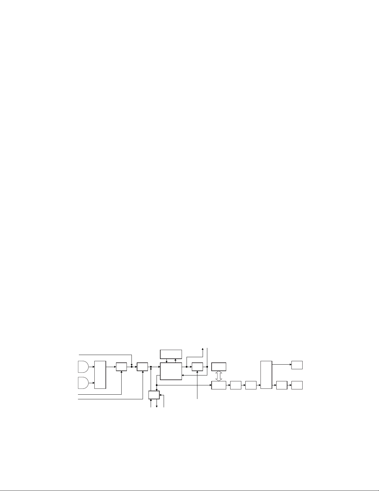
4-3. Transmit Signal Amplification Circuit
(From T/R switch to Final amplifier)
The transmit signal passing through the T/R switch
(D200) is amplified to approx. 50 mW by the two transistor
amplification circuits (Q200, Q210). The transmit signal
output from Q210 passes through an attenuator to improve
high-frequency signal matching is amplified by the drive
amplifier (Q202) and applied to the final amplifier (Q205). The
signal applied to the final amplifier is amplified by the final
amplifier so that the antenna output is 4 W (1 W for Low
Power).
4-4. High-Frequency Signal Switch Circuit
(From Antenna switch to ANT output)
The transmit signal output from the final amplifier (Q205)
passes through the antenna switch (D202, D203) and LPF,
and goes into the SPDT switch (IC202, IC203) which changes
the antenna connector (CN204) and the universal connector
(CN205).
The transmit signal passing through the output change
switch passes through the surge protection HPF and
spurious removing LPF and then goes to the antenna
connector (CN204) or the universal connector (CN205),
specified by the SPDT switch (IC202, IC203).
4-5. APC Circuit
The APC circuit detects the current of the drive amplifier
(Q202) and final amplifier (Q204) during transmission and
controls the output power by controlling the current.
It detects the current using R220 and R222 and applies a
drop voltage between both resistors during transmission to
APC (IC201). It controls the transmission current of the drive
amplifier and final amplifier so that it is constant by
comparing this current with the reference voltage output
from pin 7 of IC200. The reference voltage input to pin 5 of
IC200 is output from the DAC (IC462). High/Low power
output is set according to the DAC output voltage.
18
EXT.MIC
MIC(MAIN)
MIC(SUB)
MSW/CTS
MM
IC705
N/C
AMP
Scrambler board
Q454SWIC8
SCSW
MIC
Q455
SW
D450,D451
DET
Q452
SW
VGS-1 VATS
IC450
SW
AGC-AMP
IC452
LPF
Fig. 6 Audio band and Base band circuit
DSP
IC454
CODEC
IC456
LPF
IC459
BUFF
IC462
DAC
IC463
AMP
Q107
VCO
X100
VCXO
CIRCUIT DESCRIPTION
T/R
IC100
V-assist
DC AMP
LE
DAT
CLK
Q109 Q112 D200
to pre-pre-drive
LPF
Q106,Q107
VCO
BUFF BUFF SW
UL CV
IC5
IC101 D308
to 1st mixer
(Q200)
(IC302)
CPU
PLL
Q110,Q111
Doubler
SW
MOD
X100 IC462
VCXO DAC
4-6. Temperature Protection Circuit
The temperature protection circuit reduces the APC
voltage when the temperature of Q204 rises, to prevent
thermal destruction of the final amplifier (Q204). The CPU
D200
T/R SW
Q200
Pre Pre
Drive Amp
Q210
Pre
Drive Amp
Attenuator
Q202
Drive Amp
Fig. 7 Transmitter circuit
TK-5310
(IC5) detects the temperature with a thermistor (TH200) to
control the reference voltage to the APC circuit.
Q204
Final Amp
D202,D203
ANT SW
R220+BR222
IC201
APC
LPF
IC202
SPDT
IC203
SPDT
APC SW
CN204
CN205
5. PLL Frequency Synthesizer
The PLL Frequency Synthesizer consists of the following
components:
• VCXO (X100)
• VCO (Q106, Q107)
• Doubler (Q110, Q111)
• PLL IC (IC101)
• Local switch (D200, D308)
5-1. VCXO (X100)
VCXO (X100) generates a reference frequency of 16.8
MHz for the PLL frequency synthesizer. This reference
frequency is applied to pin 8 of the PLL IC (IC101).
The VCXO oscillation frequency is fine-adjusted by
controlling the voltage applied to pin 1 of the VCXO with DAC
(IC462). It is also controlled with pin 1 of the VCXO if the
output from VCXO is modulated.
5-2. VCO
There is a RX VCO and a TX VCO.
The TX VCO (Q107) generates a transmit carrier and the
RX VCO (Q106) generates a 1st local receive signal.
The oscillation frequency is as follows.
K, K2, and K3 types
Q106 : 400.050 ~ 449.995MHz
Q107 : 450.000 ~ 520.000MHz
K4, K5, and K6 types
Q106 : 330.050 ~ 379.995MHz
Q107 : 380.000 ~ 470.000MHz
The VCO oscillation frequency is determined by one
system of operation switching terminal "T/R" and two
systems of voltage control terminals "C/V" and "V-assist".
The operation switching terminal, "T/R", is controlled by the
control line (T/R) output from the CPU (IC5). When the T/R
logic is low, the VCO (Q107) outputs the transmit carrier and
when it is high, VCO (Q106) outputs a 1st local receive signal.
The voltage control terminals, "CV" and "V-assist", are
controlled by the PLL IC (IC101) and CPU (IC5) and the output
frequency changes continuously according to the applied
voltage. “V-assist” is controlled directly by a microcomputer
to change the VCO oscillation frequency at high speed.
However, its accuracy is low and the VCO frequency cannot
be matched accurately with the desired transmit carrier or
the 1st local receive signal. “CV” is controlled by the PLL and
is used to accurately match (look) the desired frequency of
the VCO oscillation frequency. For the modulation input
terminal, "MOD", the output frequency changes according to
the applied voltage. This is used to modulate the VCO output.
"MOD" works only when "T/R" is low.
5-3. Doubler (Q110, Q111)
The doubler (Q110, Q111) extracts the twice harmonic
component from the signal output from the VCO. This twice
harmonic component is then fed into pin 5 of the PLL IC.
5-4. PLL IC (IC101)
PLL IC compares the differences in phases of the VCO
oscillation frequency and the VCXO reference frequency,
returns the difference to the VCO CV terminal and realizes
the "Phase Locked Loop" for the return control. This allows
the VCO oscillation frequency to accurately match (lock) the
desired frequency.
When the frequency is controlled by the PLL, the
frequency convergence time increases as the frequency
difference increases when the set frequency is changed. To
supplement this, the CPU is used before control by the PLL
IC to bring the VCO oscillation frequency close to the desired
frequency. As a result, the VCO CV voltage does not change
and is always stable at approx. 2.5 V.
The desired frequency is set for the PLL IC by the CPU
(IC5) through the 3-line "LE", "DAT", "CLK" serial bus. Whether
the PLL IC is locked or not is monitored by the CPU through
the “UL” signal line. If the VCO is not the desired frequency
(unlock), the "UL" logic is low.
5-5. Local Switch (D200, D308)
The connection destination of the signal output from the
VCO is changed with the diode switch (D200) that is
controlled by the transmission power supply, 5T, and the
diode switch (D308) that is controlled by the receive power
supply, 5R.
If the 5T logic is high, it is connected to a send-side prepre-drive (Q200). If the 5T logic is low, it is connected to a
receive-side mixer (IC302).
Fig. 8 PLL block diagram
19
TK-5310
CIRCUIT DESCRIPTION
6. Control Circuit
The control circuit consists of CPU (IC5) and its peripheral
circuits. It controls the TX-RX unit and transfers data to the
Control unit. IC5 mainly performs the following;
1) Switching between transmission and reception by PTT
signal input.
2) Reading system, zone, frequency, and program data from
the memory circuit.
3) Sending frequency program data to the PLL.
4) Controlling squelch on/off by the DC voltage from the
squelch circuit.
5) Controlling the audio mute circuit by decode data input.
6) Transmitting tone and encode data.
6-1. Memory Circuit
Memory circuit consists of the CPU (IC5) and a flash
memory (IC6). A flash memory has a capacity of 16M bits and
contains the transceiver control program for the CPU. It also
stores the data for transceiver channels and operating parameter that are written by the FPU. This program can be easily
written from an external devices.
The EEPROM (IC3) stores the last channel data, the scan
on status, and other parameters.
■ Flash memory
Note : The flash memory stores the data that is written by
the FPU (KPG-95D), and firmware program (User mode, Test
mode, Tuning mode, etc.). This data must be rewritten when
replacing the flash memory.
■ EEPROM
Note : The EEPROM stores tuning data (Deviation, Squelch,
etc.).
Realign the transceiver after replacing the EEPROM.
■ Real-time clock
The clock function is based on real-time clock IC (IC2).
When the power supply is off, it is backed up by an internal
secondary lithium battery
IC5
CPU
IC3
EEPROM
6-2. LCD (K2, K3, K5 and K6 models only)
The LCD is controlled using the bus lines on the connector
(CN800) of the control unit (X57 B/5).
The LCD contrast voltage is corrected using IC800. The
thermometry result used by the temperature IC (IC1) is
corrected by the CPU (IC5), and the contrast voltage is output
as a pulse ripple from the LCDV terminal (pin 28) of the CPU.
The filter then smoothens the voltage which in turn is input
into pin 3 of IC800.
6-3. Temperature Detection Circuit
The temperature detection circuit detects the
temperature using a temperature IC (IC1) and corrects the
thermal characteristic change of the squelch or LCD.
6-4. Key Detection Circuit
Keys are detected using three shift registers (IC801,
IC802, IC803).
The KIN signal that is normally pulled down goes high
when any key is pressed.
6-5. Low Battery Warning
The battery voltage is divided using R22 and R23 and is
detected by the CPU (IC5). When the battery voltage falls
below the voltage set by the Low battery warning
adjustment, the red LED blinks to notify the operator that it is
time to replace the battery. If the battery voltage falls even
more (approx. 5.8V), a beep sounds and transmission stops.
Low battery warning Battery condition
The red LED blinks during The battery voltage is low but
transmission. the transceiver is still usable.
The red LED blinks and The battery voltage is low and
the warning tone beeps while the transceiver is not usable to
the PTT switch is pressed. make calls.
6-6. Battery Type Detection
The transceiver automatically detects the battery type,
measuring the resistance between the S-terminal and GND
terminal on the battery pack and changes the supplied
voltage to the S-terminal as below. The microprocessor then
detects the battery type.
20
IC5
CPU
IC8
DSP
IC457
FPGA
IC454
CODEC
FLASH
IC6
Fig. 9 Memory circuit
9.216MHz
9.216MHz
IC453
(2/3,3/3)
18.432MHz
18.432MHz
Fig. 10 Clock diagram
IC455
IC453
(1/3)
X450
VCXO
18.432MHz
Battery type Input voltage of S-terminal Resistor value
Battery case 0~0.2V Short
Li-ion battery 0.85~1.02V 47 kΩ
Ni-Cd battery 3.23~3.37V Open
Ni-MH battery 1.71~1.95V 150 kΩ
6-7. VOX
The VOX function can be used only with an external
microphone.
The VOX (Voice Operated Transmission) function detects
voice input to the microphone and automatically switches
between transmission and reception. However, if a
scrambler board is installed (Extended Function Voice
Scrambler is selected with FPU), VOX does not operate.
CIRCUIT DESCRIPTION
TK-5310
If the microphone input exceeds a certain level,
transmission automatically begins. If the input falls below a
certain level, the transceiver automatically returns to receive
mode.
The transceiver realizes this function using DSP (IC8).
6-8. DSP
The DSP circuit consists of a DSP (IC8), a CODEC (IC454)
and processes the base band signal. The DSP operates on an
external clock of 9.216MHz (the same as the CPU), the I/O
section operates at 3.3V and the core section operates at
1.5V. The DSP carries out the following processes:
• C4FM encoding
• Analog FM pre-emphasis/de-emphasis
• Vocoder (IMBE) processing between audio codec and
modulation/demodulation
• CAI processing, such as error correction encoding
• QT/DQT encoding/decoding
• DTMF encoding/decoding
• MSK encoding/decoding
• 2-tone encoding/decoding
• Compressor/expander processing
• Transmit/receive audio filtering processing
• VOX processing
•Microphone amplifier AGC processing
• Audio mute processing
•Modulation level processing
6-9. FPGA
The FPGA(IC457) I/O section operates at 3.3V. and the core
section operates at 2.5V. The FPGA has the following function.
• Demodulation (C4FM,CQPSK)
• Shift register(8CH)
• Level convert Buffer amplifier(5V➝3.3V)(9CH)
• Generates 1.536MHz for the demodulation and CODEC.
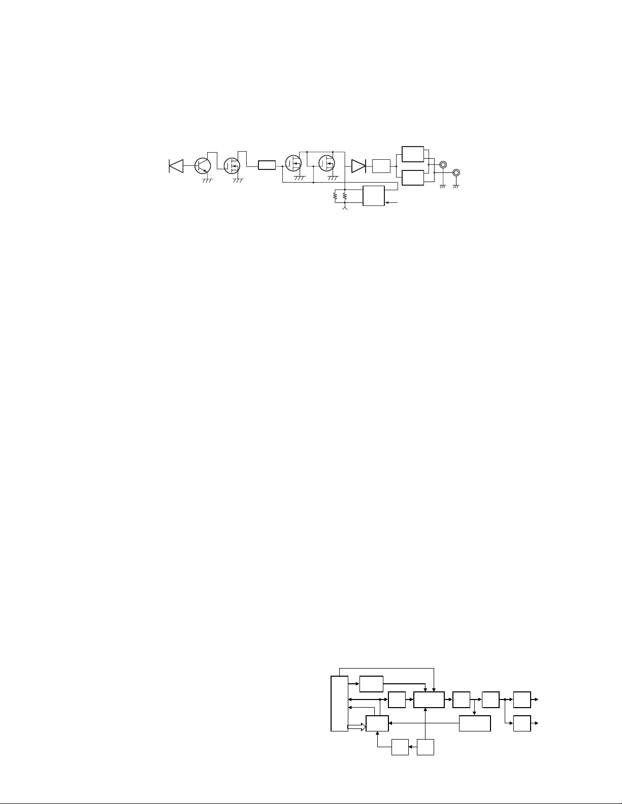
7. Power Supply Circuit
The power supply voltage (+B) is supplied from the
battery terminal of the TX-RX unit (X57 A/5) and is then
passed through the fuse (F600).
If +B voltage is detected by the voltage detection IC
(IC706) and it is above 5.6V, then the 3V regulator (IC704) CE
pin becomes high and the 3.0V power source turns ON.
Additionally, when the VOL SW is ON, the 3.6V DC/DC
converter (IC710) CE pin becomes high and the 3.6V power
source turns ON.
The output from the 3.6V DC/DC converter (IC710)
provides the power source for three regulators (IC707,
IC708, IC711) and the 1.5V DC/DC converter (IC709).
The voltage output from the 1.5V DC/DC converter
(IC709) is detected by the 33A SW (Q712).
When the CE pin of the 3.3V regulator (IC708) is high, the
33A power source turns on.
When the 3.6V power source turns on, the 5V regulator
(IC712) CE pin becomes high and 5M is supplied with the
power source.
The three regulators (IC707, IC708, IC711) and the DC/DC
converter (IC709) start the CPU, DSP, FPGA, etc. After the
CPU starts up, it begins controlling two regulators (IC601,
IC600) with the 5CC and PWR signals.
When the Power SW (Q602) is turned on with the PWR
signal, the 15V DC/DC converter (IC713) starts up. IC712,
IC601, and IC600 is supplied from +B.
The output from IC600 is switched between 5R (which is
turned on while receiving) and 5T (which is turned on while
transmitting), and is controlled by the CPU.
The output from of the 5V regulator (IC610) is controlled by
Q604 and is used as a power source for 5MCS, for an optional
accessory which is connected to the universal connector.
Drive, Final AMP
+B
33M
33A
28M
15D
25D
15V
Q604
5M CS SW
5MC
5C
Q601
5R SW
CE
5RC
Q600
5T SW
CE
5TC
DC/DC, AVR
CPU, FlashROM,
EEPROM, VCXO,
FPGA (I/O)
DSP (I/O)
RTC
DSP (Core)
FPGA (Core)
LCD
VCO
5M
5MCS
5R
5T
F600
3A Fuse
BATT
+B
CE
IC704
AVR IC
CE
VOL
SW
Q713
Detect
IC706
Detect
Q602
Power
SW
IC5
CPU
SW
SB
PWR
IC710
DC/DC
3.6V
Q712
33A SW
5CC
IC707
AVR IC
CE
IC708
AVR IC
CE
IC709
DC/DC
CE
IC711
AVR IC
CE
IC713
DC/DC
CE
IC712
AVR IC
CE
CE
IC610
AVR IC
IC601
AVR IC
CE
IC600
AVR IC
CE
Fig. 11
8. Signaling Circuit
8-1. Encode (QT/DQT/DTMF/2-tone/MSK)
Each signaling data signal of QT, DQT, DTMF, 2-tone and
MSK is generated by the DSP circuit, superposed on a modulation signal and output from pin 16 of the CODEC (IC406).
The modulation balance of the QT/DQT signal is adjusted
by the D/A converter(IC411) and the resulting signal is routed
to the modulation input of the VCO and VCXO (X301).
The each deviation of the TX QT, DQT, DTMF, 2-tone and
MSK tone is adjusted by changing the output level of the
CODEC and the resulting signal is routed to VCO and VCXO.
The RX DTMF tone is output from pin 15 of the CODEC,
passes through the receive audio signal system, and is output from the speaker.
8-2. Decode (QT/DQT/DTMF/2-tone/MSK)
The audio signal is removed from the FM detection signal
sent to the DSP circuit and the resulting signal is decoded.
9. Compander Circuit
The term “compander” means compressor and expander.
The compander reduces noise by utilizing a compressor and
an expander.
The transceiver contains DSP(IC8) to perform this operation. The transceiver compander can be turned on or off using
the FPU.
21
TK-5310
SEMICONDUCTOR DATA
CPU:30625MGP346HU (TX-RX unit IC5)
Pin
Port Name I/O Function
No.
1 BATT DET I(A/D) Battery detection terminal
2 NC(ANEX0) I NC (For expansion A/D)
3 ASSIST O
4 VOICE O
5 SOE O Shift register OE
6ULIPLL unlock input
7DAT O Common data
8 CLK O Common clock
9 SDA I/O EEPROM data
10 BYTE I Use as 8bit data bus (Vcc)
11 CNVSS I Use as memory expansion mode (Vss)
12 STRB O Shift register CS
13 NC - No connection
14 RESET I Reset input
15 XOUT - No connection
16 VSS1 - Power supply input
17 XIN - Clock input, 9.216MHz(18.432MHz/2)
18 VCC1 - Power supply input
19 NMI I NC
20 RTCDT I/O RTC data I/O
21 PSW I
22 INTRA I
23 LD O DAC LD
24 BEEP
25 LE O PLL CS
26 BSFT O Beat shift output
27 KEY/PLAY I TX key input (for ANI board),
28 LCDV O LCD contrast adjustment
29 INH I Audio inhibit input (for ANI board),
30 AUXI I AUX input (for ANI board),
31 TCNT I Tone control input (for ANI board),
32 BEEPS O Beep switch(L:Unmute, H:Mute)
33 TXD1
34 VCC1 - Power supply input
35 RXD1 I
36 VSS2 - Power supply input
37 BUSY I BUSY input(for VGS)
38 RTSM/EXTO O UART(3.3V➔5V)/External option
39 TXDM
40 RXDM I
41 DSRM I UART(5V➔3.3V)
42 CTSM I UART(5V➔3.3V)
43 A20 O Flash memory A19
44 KES O Key counter CS
45 KIN I Key counter return
46 MODEL I Model detection
47 RDY I Bus control (Ready)
48 ALE - No connection
49 HOLD I Bus control (Hold)
(D/A)
VCO control
(D/A)
Voice output
(INT1)
Power switch detection
(L:Power on, H:Power off)
(INT0)
RTC interrupt input
O
(PWM)
Beep output
(L:Shift, H:Not shift)
Play Input (for VGS)
O
(UART)
UART(for VGS)
(UART)
UART(for VGS)
output port to universal connector
O
(UART)
UART(3.3V➔5V)
(UART)
UART(5V➔3.3V)
Pin
Port Name I/O Function
No.
50 HLDA - No connection
51 WN O Wide/Narrow ceramic filter switching
(L:Narrow, H:Wide)
52 VN O Wide,Narrow/P25 ceramic filter
switching (L:P25, H:Analog)
53 EXTIM I External option control port from
universal connector
54 SCSW O When the scrambler board is installed,
the route of AF is changed.
(L:Scrambler on, H:off)
55 BCLK O Bus control (Base clock output)
56 RD O Bus control (Read)
57 BHE - No connection
58 WR O Bus control (Write)
59 TGL0 I Lever switch input 0
60 TGL1 I Concentric switch input 1
61 TGL2 I Concentric switch input 2
62 CS3 O LCD CS
63 CS2 O Flash memory CS
64 CS1 O DSP CS
65 CS0 O Flash memory CS
66 A19 O Address bus 19
67 A18 O Address bus 18
68 A17 O Address bus 17
69 A16 O Address bus 16
70 A15 O Address bus 15
71 A14 O Address bus 14
72 A13 O Address bus 13
73 A12 O Address bus 12
74 A11 O Address bus 11
75 A10 O Address bus 10
76 A9 O Address bus 9
77 INAFC O Internal AF control (L:Off, H:On)
78 CH_A I Rotary switch input 1
79 CH_B I Rotary switch input 2
80 CH_C I Rotary switch input 3
81 CH_D I Rotary switch input 4
82 VCC2 - Power supply input
83 A8 O Address bus 8
84 VSS3 - Power supply input
85 A7 O Address bus 7
86 A6 O Address bus 6
87 A5 O Address bus 5
88 A4 O Address bus 4
89 A3 O Address bus 3
90 A2 O Address bus 2
91 A1 O Address bus 1
92 A0 O Address bus 0
93 EXAFC O External AF Control (L:Off, H:On)
94 HINT I(INT4) DSP HINT interrupt
95 INT3 - Not used
96 PTT I PTT input
97 EXSP I External speaker install check
98 DRST O DSP reset output
22
SEMICONDUCTOR DATA
TK-5310
Pin
Port Name I/O Function
No.
99 FRST O Flash memory reset output
100 NC O No connection
101 D7 I/O Data bus 7
102 D6 I/O Data bus 6
103 D5 I/O Data bus 5
104 D4 I/O Data bus 4
105 D3 I/O Data bus 3
106 D2 I/O Data bus 2
107 D1 I/O Data bus 1
108 D0 I/O Data bus 0
109 5TC O 5T control (L:Off, H:On)
110 5RC O 5R control (L:Off, H:On)
111 5CC O 5C control (L:Off, H:On)
112 APCSW O APC switch output (L:Off, H:On)
113 CAE3 I Man-down switch input
114 VU I V/U detection
115 MM O MIC mute output (L:Unmute, H:Mute)
116 PWR O Power control output
(L:Power off, H:Normal)
117 WPA I(A/D) PA temperature compensation
118 SQ I(A/D) Analog SQ input
119 CV I(A/D) VCO CV input
120 RSSI I(A/D) RSSI input
121 TEMP I(A/D) Temperature input
122 BATT I(A/D) Battery level input
123 REM I(A/D) KMC-25 PF1/PF2 key, KVL3000 input
124 AVSS -
125 VOL I(A/D) Volume level input
126 VREF - A/D converter reference voltage input
127 AVCC - A/D converter power supply input
128 T/R O TX/RX switch (L:TX, H:RX)
A/D converter power supply input terminal
terminal
terminal
Shift Register:BU4094BCFV (TX-RX unit IC606)
Pin
Port Name I/O Function
No.
1 STRB I Latch clock input
2 DATA I Serial data input
3 CLK I Serial clock input
4Q1OOPT5
5Q2OOPT4
6Q3OOPT1
7Q4 OOP_MAN
8 VSS - GND
9QSOSerial data output
10 Q'S O NC
11 Q8 O OPT6
12 Q7 O OPT2
13 Q6 O CHGIO:UNIV 9p I/O Switching
14 Q5 O OPT3
15 OE I Output enable control input
16 VDD - Power supply input
Shift Register:BU4094BCF (Control unit IC801)
Pin
Port Name I/O Function
No.
1 STRB I Latch clock input
2 DATA I Serial data input
3 CLK I Serial clock input
4-7 Q1-Q4 O Key counter
8 VSS - GND
9QSOSerial data output
10 Q’S O NC
11-14 Q8-Q5 O Key counter
15 OE I Output enable control input
16 VDD - Power supply input
Shift Register:BU4094BCF (Control unit IC802)
Pin
Port Name I/O Function
No.
1 STRB I Latch clock input
2 DATA I Serial data input
3 CLK I Serial clock input
4-7 Q1-Q4 O Key counter
8 VSS - GND
9QSOSerial data output
10 Q’4 O NC
11-14 Q8-Q5 O Key counter
15 OE I Output enable control input
16 VDD - Power supply input
Shift Register:BU4094BCF (Control unit IC803)
Pin
Port Name I/O Function
No.
1 STRB I Latch clock input
2 DATA I Serial data input
3 CLK I Serial clock input
4-7 Q1-Q4 O Key counter
8 VSS - GND
9OS ONC
10 NC O NC
11 Q8 O Audio amplifier switch
12 Q7 O Backlight switch
13 Q6 O TX LED switch
14 Q5 O Busy LED switch
15 OE I Output enable control input
16 VDD - Power supply input
23
TK-5310
COMPONENTS DESCRIPTION
TX-RX unit (X57-7250-XX A/5)
Ref. No. Part name Description
IC1 IC Temperature DET
IC2 IC RTC IC
IC3 IC EEPROM
IC4 IC Voltage DET
IC5 IC CPU
IC6 IC FLASH ROM
IC7 IC CS AND
IC8 IC DSP
IC100 IC DC AMP for VCO tune
IC101 IC PLL IC
IC200 IC DC AMP
IC201 IC Auto Power Control
IC202,203 IC SPDT
IC300,301 IC DC AMP for BPF
IC302 IC DBM
IC303 IC Multiplexer
IC304 IC FM IC
IC305~307 IC Multiplexer
IC308 IC Buffer
IC450 IC Switch (VGS TX I/O)
IC451 IC OP AMP (5V reference/SQL AMP)
IC452 IC OP AMP (TX AGC AMP/Buffer AMP)
IC453 IC D-type flip flop
IC454 IC CODEC
IC455 IC Buffer
IC456 IC OP AMP (TX LPF/RX LPF)
IC457 IC FPGA
IC458 IC Switch (RX scrambler SW/BEEP SW)
IC459 IC
IC460 IC Switch (VGS RX I/O)
IC461 IC RX summing AMP
IC462 IC D/A Converter
IC463 IC
IC600 IC Voltage regulator (5T/5R)
IC601 IC Voltage regulator (5C)
IC602 IC Multiplexer
IC603 IC Buffer
IC604,605 IC UART switch
IC606 IC Shift register
IC607 IC Bus switch (8ch)
IC608,609 IC Bus switch (2ch)
IC610 IC Voltage regulator (5MCS)
Q100 Transistor Ripple filter
Q101 FET S33A switch
Q102 FET Switch
Q103 FET Buffer for CV
Q104 Transistor Ripple filter
Q105 FET T/R switch
Q106,107 Transistor VCO oscillation
Q108 FET T/R switch
Q109~112 Transistor Buffer AMP
Q200 Transistor RF AMP
Q202 FET RF driver AMP
Q203 FET APC switch
Q204 FET RF final AMP
24
OP AMP (TX buffer AMP/RX buffer AMP)
OP AMP (TX MOD AMP/3.3V reference)
Ref. No. Part name Description
Q205 Transistor 3.3V➝5V level converter
Q206 FET APC switch
Q207 Transistor APC switch
Q208 FET APC switch
Q209 FET SPDT EXT/INT switch
Q210 Transistor RF AMP
Q300 Transistor Ripple filter
Q301 FET LNA (Low Noise AMP)
Q302 FET IF AMP
Q303 Transistor 2nd local buffer AMP
Q304 Transistor W/N switch
Q450,451 Transistor Auto gain control
Q452 FET MIC mute switch
Q453 FET VGS I/O switch
Q454 FET TX scrambler switch
Q455 FET EXT MIC switch
Q456 FET TX scrambler switch
Q457 FET EXT MIC switch
Q459 FET Beat shift switch
Q460 Transistor Noise AMP
Q461 FET VGS I/O switch
Q600 FET 5T switch
Q601 FET 5R switch
Q602 FET SB switch
Q603 FET 5M switch
Q604 FET 5M switch
Q605 FET 5V➝3.3V level converter
Q606 FET Switch
D1 Diode Reverse current prevention
D102
D104~112
D113,114 Diode Feedback filter switch
D115
D116,117 Diode Feedback filter switch
D118 Diode 5C voltage rise
D119 Diode Bypass diode
D200 Diode Local switch
D201 Zener diode Voltage protection
D202~205 Diode Antenna switch
D206,207 Varistor Surge absorption
D301,302
D304~307
D308 Diode Local switch
D450,451 Diode Detection
D452 Diode Reverse current prevention
D453 Diode Detection
D454,455 Diode Reverse current prevention
D600 Diode Reverse current prevention
D601,602 Varistor Surge absorption
D609,611 Diode Surge absorption
Variable
capacitance diode
Variable
capacitance diode
Variable
capacitance diode
Variable
capacitance diode
Variable
capacitance diode
Frequency control
Frequency control
FM modulation
Vari-cap tune
Vari-cap tune

COMPONENTS DESCRIPTION
TK-5310
Control unit (X57-7250-XX B/5)
Ref. No. Part name Description
IC701 IC AF mute switch
IC702,703 IC Audio AMP
IC704 IC Voltage regulator (28M)
IC705 IC OP AMP (AF Pre-AMP/TX AF AMP)
IC706 IC Voltage detector (5.6V)
IC707 IC Voltage regulator (33M)
IC708 IC Voltage regulator (33A)
IC709 IC DC/DC converter (15D)
IC710 IC DC/DC converter (36M)
IC711 IC Voltage regulator (25D)
IC712 IC Voltage regulator (5M)
IC713 IC DC/DC converter (15V)
IC800 IC DC AMP for LCD voltage
IC801~803 IC Shift register
Q700 FET 5A AVR switch
Q701 Transistor 5A AVR switch
Q702 Transistor 5A AVR
Q703,704 FET External audio mute switch
Q705,706 FET Internal audio mute switch
Q708 FET EXT/INT gain convert switch
Q709 Transistor Noise canceler switch
Q710 FET Switch (36M DC/DC)
Q711 FET Switch (15V DC/DC)
Q712 FET DSP power supply timing control
Q713 FET DC/DC converter (36M) control
Q800,801 Transistor switch (backlight)
Q802 FET PSW switch
Q803 FET Busy LED switch
Q804 FET TX LED switch
D700,701 diode Reverse current prevention
D702 diode Surge absorption
D703 diode Reverse current prevention
D704 diode flywheel (DC/DC)
D705~708 diode Reverse current prevention
D800~803 LED Key backlight
D804,805 diode Reverse current prevention
D806~809 LED Key backlight
D810~812 LED LCD backlight
D813,814 diode Reverse current prevention
D815 Zener diode AVR for backlight LED
D816~818 diode Reverse current prevention
Top Panel unit (X57-7250-XX C/5)
Ref. No. Part name Description
D901 LED TX/RX LED
25

TK-5310
PARTS LIST
CAPACITORS
1 = Type ... ceramic, electrolytic, etc.
2 = Shape ... round, square, ect.
3 = Temp. coefficient
Temperature coefficient
1st Word
Color*
ppm/
Tolerance (More than 10pF)
Code
(%)
Voltage rating
1st word
Black Red Orange Yellow Green Blue Violet
0 -80 -150 -220
C
0.25 0.5 2 5 10 20
2nd word
0
1
2
3
CC 45
1
1
2
LCPRSTU
DG J KMX Z P
A
BCD EF
1.0
1.25
10
12.5
100
125
1000
1250
TH 1H J220
3
4
5
4 = Voltage rating
5 = Value
6 = Tolerance
2.0
1.6
20
16
200
160
2000
1600
6
-330 -470 -750
+ 40
+ 80
- 40
- 20
3.15
2.5
31.5
25
315
250
3150
2500
CC45
+ 100
-0
G
4.0
40
400
4000
Color*
2nd Word HG
ppm/
Example : CC45TH = -470
No code
More than 10µF -10 +50
Less than 4.7µF -10 +75
H
J
5.0
6.3
50
63
500
630
5000
6300
Capacitor value
010 = 1pF
100 = 10pF
101 = 100pF
102 = 1000pF = 0.001µF
103 = 0.01µF
30 60
K
V
8.0
-
80
35
800
-
8000
-
22
JKL
120 250 500
60ppm/
(Less than 10pF)
Gode
(pF)
CD FGB
0.1 0.25 0.5 1 2
0 = 22pF
Multiplier
2nd number
1st number
Chip capacitors
(EX) C C 7 3 F S L 1 H
(Chip)(CH,RH,UJ,SL)
(EX) C K 7 3 F F 1 H
(Chip)(B,F)
RESISTORS
Chip resistor (Carbon)
(EX) R D 7 3 E B 2 B
(Chip)(B,F)
Carbon resistor (Normal type)
(EX) R D 1 4 B B
1 = Type
2 = Shape
3 = Dimension
4 = Temp. coefficient
2C
000
000
000
000
J
7654321
Z
7654321
J
7654321
J
7654321
5 = Rating wattage
6 = Value
7 = Tolerance
Refer to the table above.
1 = Type
2 = Shape
3 = Dimension
4 = Temp. coefficient
5 = Voltage rating
6 = Value
7 = Tolerance
Dimension (Chip capacitors)
Dimension code L W T
Empty
A
B
C
D
E
F
G
H
Dimension
Dimension (Chip resistor)
Dimension code L W T
E
F
G
H
Rating wattage
Wattage
Code
1/16W
1J
1/10W
2A
1/8W
2B
5.6
4.5
4.5
4.5
3.2
3.0
2.0
1.6
1.0
W
3.2
2.0
1.6
1.0
Code
2C
2E
2H
L
0.5
0.5
0.5
0.5
0.4
0.2
0.3
0.2
0.05
0.2
0.3
0.2
0.05
Wattage
1/6W
1/4W
1/2W
5.0
3.2
2.0
1.25
2.5
1.6
1.25
0.8
0.5
1.6
1.25
0.8
0.5
Code
0.5
0.4
0.3
0.2
0.3
0.2
0.2
0.2
0.05
T
0.2
0.2
0.2
0.05
3A
3D
Less than 2.0
Less than 2.0
Less than 2.0
Less than 1.25
Less than 1.5
Less than 1.25
Less than 1.25
Less than 1.0
0.35
Wattage
1W
2W
0.5
0.5
0.05
1.0
1.0
0.1
0.05
2626

PARTS LIST
TK-5310
New Parts. indicates safety critical components.
∗
Parts without Parts No. are not supplied.
Les articles non mentionnes dans le Parts No. ne sont pas fournis.
Teile ohne Parts No. werden nicht geliefert.
TK-5310 (Y50-6060-XX)
Ref. No.
Address
Parts No. Description
parts
Destination Destination
New
TK-5310
11A A02-3875-01 MAIN CABINET K,K4
21D A02-3877-11 MAIN CABINET(4KEY) K2,K5
31D∗ A02-3879-11 MAIN CABINET(DTMF) K3,K6
4 3A,3C ∗ A10-4084-31 CHASSIS
5 2B,2D A62-1104-02 PANEL(TOP)
6 3A,3C A82-0057-02 REAR PANEL
7 2B,2D B03-3612-04 DRESSING PLATE(16CH)
8
9 2B,2D B11-1821-03 ILLUMINATION GUIDE(TX-BUSY)
10 1C B11-1832-04 FILTER(LCD) K2,K3,K5
10 1C B11-1832-04 FILTER(LCD) K6
11 1C ∗ B38-0891-15 LCD ASSY K2,K3,K5
11 1C ∗ B38-0891-15 LCD ASSY K6
12 3A,3C B41-1841-04
13 1B,1D B43-1171-04 BADGE(FRONT)
14 2B,2D B43-1172-04 BADGE(REAR)
15 2E B59-2393-00
16 2E ∗ B59-2439-00
17 2E ∗ B59-2448-00
18 2E ∗ B62-1972-00
20 3A ∗ B72-2418-04 MODEL NAME-PLATE K
21 3C ∗ B72-2419-04 MODEL NAME-PLATE K2
22 3C ∗ B72-2420-04 MODEL NAME-PLATE K3
23 3A ∗ B72-2421-04 MODEL NAME-PLATE K4
24 3C ∗ B72-2422-04 MODEL NAME-PLATE K5
25 3C ∗ B72-2423-04 MODEL NAME-PLATE K6
27 2A,2C E37-0722-05 LEAD WIRE WITH CONNECTOR(UNIV)
28 2B,2D E37-1126-15 LEAD WIRE WITH CONNECTOR(ANT)
29 2C E37-1128-05 FLAT CABLE(CN613-CN800) K2,K3,K5
29 2C E37-1128-05 FLAT CABLE(CN613-CN800) K6
30 3A,3C E58-0510-05 RECTANGULAR RECEPTACLE(UNIV)
31 3A,3C E72-0420-33 TERMINAL BLOCK(BATT+)
32 3A,3C F07-1887-12 COVER ASSY
33 2A,2C F10-2499-12 SHIELDING PLATE(TX-RX PCB)
34 3A,3C G10-1327-04 FIBROUS SHEET(AIR)
35 1B,1D G10-1338-04 FIBROUS SHEET(SP)
36 3A,3C ∗ G10-1366-04 FIBROUS SHEET
37 1C G11-4302-04 SHEET(LCD) K2,K3,K5
37 1C G11-4302-04 SHEET(LCD) K6
38 3A,3C G11-4303-14 SHEET(PTT)
39
40 - G11-4346-08 SHEET(UNIV)
41 1A,1C G13-2036-04 CUSHION(MIC)
42
43 1A,2C, G13-2070-04 CUSHION(CORD ASSY)
44 2A,2C G13-2071-04 CONDUCTIVE CUSHION(CHASSIS/PCB)
45 2B,2D G13-2079-04 CUSHION(VOL)
46 1C G13-2087-04 CUSHION(LCD) K2,K3,K5
46 1C G13-2087-04 CUSHION(LCD) K6
47 2B,2D G53-1628-04 PACKING(VOL TORQ-UP)
48 2B,2D G53-1629-05 PACKING(VOL,CH O-RING)
49 2B,2D G53-1630-05 PACKING(ANT O-RING)
1B,1D,2E
1B,1D,2E
3A,2C,3C
3A,3C
B09-0682-13 CAP(SP/MIC) ACCESSORY
CAUTION STICKER(HUMAN BODY PROTECTION)
SUB-INSTRUCTION MANUAL(QRC/ENGLISH)
SUB-INSTRUCTION MANUAL(QRC/FRENCH)
PAMPHLET(HUMAN BODY PROTECTION)
INSTRUCTION MANUAL(ENGLISH/FRENCH)
G11-4340-04 RUBBER SHEET(CAP) ACCESSORY
G13-2046-04 CUSHION(UNIV)
L:
Scandinavia
Y:
PX (Far East, Hawaii)
Y:
AAFES (Europe)
Ref. No.
50 2B,2D G53-1631-05 PACKING(LEVER SW O-RING)
51 1B,1D G53-1633-04 PACKING(SP)
52 1B,1D, G53-1634-14 PACKING(MAIN MIC,NC MIC)
53 2A,2C G53-1637-04 PACKING(CHASSIS-FRONT)
54 2B,2D G53-1638-04 PACKING(CHASSIS-TOP)
55 3A,3C G53-1640-03 PACKING(BATT)
56 3A,3C G53-1649-05 PACKING(BATT- O-RING)
57 3A,3C G53-1663-23 PACKING(TERMINAL BLOCK)
59 3F ∗ H52-2174-02 ITEM CARTON CASE
60 1C J19-5475-12 HOLDER(LCD) K2,K3,K5
60 1C J19-5475-12 HOLDER(LCD) K6
61 2B,2D J19-5477-04 HOLDER(EMG)
62 2B,2D ∗ J21-8482-13 MOUNTING HARDWARE(TOP)
63 2B,2D J21-8483-03 MOUNTING HARDWARE(SP)
64 3A,3C J21-8484-04 MOUNTING HARDWARE(NC MIC)
65 2B,2D ∗ J21-8581-04 MOUNTING HARDWARE(LEVER SW)
66 2B,2D J21-8495-04
67 2E ∗ J29-0730-05 BELT CLIP ACCESSORY
68 2B,2D J39-0646-03 SPACER(VOL)
69 2B,2D J39-0647-03 SPACER(16CH)
70 2B,2D J82-0096-05 FPC(VOL/CH)
71 3A,3C J82-0097-25 FPC(UNIV)
72 2B,2D J82-0098-05 FPC(SP/MIC)
73 2A,2C J82-0104-05 FPC(CONTROL-TOP)
74 3A,3C J99-0377-14 ADHESIVE SHEET(PTT)
75 3A,3C J99-0380-04 ADHESIVE SHEET(ANT PCB)
76 2A,2C J99-0381-04 ADHESIVE SHEET(CONTROL-TOP FPC)
77 1B,1D J99-0383-14 ADHESIVE SHEET(SP)
78 1C J99-0390-04 ADHESIVE SHEET(LCD FILTER) K2,K3,K5
78 1C J99-0390-04 ADHESIVE SHEET(LCD FILTER) K6
80 2B,2D K29-9319-03 KEY TOP(EMG)
81 1D K29-9320-03 KEY TOP(4KEY) K2,K5
82 1C K29-9321-13 KEY TOP(DTMF) K3,K6
83 2B,2D K29-9322-03 KNOB(VOL)
84 2B,2D K29-9323-03 KNOB(16CH)
85 2B,2D K29-9324-13 KNOB(CONCENTRIC SW)
86 2B,2D K29-9325-04 KNOB(LEVER SW)
87 1A,1C K29-9327-03 KEY TOP(PTT)
88 1A,1C K29-9328-02 KNOB(PTT)
A
B 2B,2D N09-2439-25 SPECIAL SCREW(SP)
C 3A,3C N09-2440-15 SPECIAL SCREW(CASE)
D 3A,3C N09-2441-15 SPECIAL SCREW(COVER ASSY)
E 2B,2D N09-2442-15 SPECIAL SCREW(ANT)
F 3A,3C ∗ N09-2443-14 HEXAGON HEAD SCREW(BATT-)
H 2B,2D N14-0813-14 CIRCULAR NUT(VOL)
I 2B,2D ∗ N14-0814-14 CIRCULAR NUT(CH)
J 2B,2D N14-0815-04 CIRCULAR NUT(ANT)
K 2B,2D ∗ N14-0817-14 HEXAGON NUT(LEVER SW)
M2E N30-3008-60
N 2B,2D N32-2004-48 FLAT HEAD MACHINE SCREW(TOP)
P 1A,1C, N83-2005-48
Address
2A,2C
1B,1D,2E
2A,2C
K:
USA
T:
England
X:
Australia
New
Parts No. Description
parts
N08-0531-14 DRESSED SCREW(CAP) ACCESSORY
P:
Canada
E:
Europe
M:
Other Areas
MOUNTING HARDWARE(LEVER SW PANEL SIDE)
PAN HEAD MACHINE SCREW(BELT CLIP)
PAN HEAD TAPTITE SCREW(CONT/TXRX)
27

TK-5310
TK-5310
TX-RX UNIT (X57-7250-XX)
Ref. No. Parts No. Description
Q 2B,2D N83-2006-43 PAN HEAD TAPTITE SCREW(TOP)
Address
New
parts
PARTS LIST
Destination Destination
Ref. No. Parts No. Description
C131 CK73HB1C103K CHIP C 0.010UF K
Address
New
parts
90 3B,3D R31-0654-05 VARIABLE RESISTOR(VOL)
91 3B,3D S60-0431-05 ROTARY SWITCH(CH)
92 1C S79-0454-05 KEYBOARD ASSY(4KEY,DTMF) K2,K3,K5
92 1C S79-0454-05 KEYBOARD ASSY(4KEY,DTMF) K6
93 1B,1D T07-0755-15 SPEAKER
94 2A,2B, T91-0575-05 MIC ELEMENTT(MAIN MIC,NC MIC)
2C,2D
95 1C W09-0971-05 LITHIUM CELL
96 3A,3C X41-3690-10 SWITCH UNIT(FPC(PTT))
97 1A,2C X42-3270-10 CORD ASSY(FPC(50PIN))
TX-RX UNIT (X57-7250-XX)
-10 :K -11 :K2 -12 :K3 -13 :K4 -14 :K5 -15 :K6
D800-803 B30-2171-05 LED K3,K6
D800,801 B30-2171-05 LED K2,K5
D806-809 B30-2171-05 LED K3,K6
D810-812 B30-2261-05 LED K2,K3,K5
D810-812 B30-2261-05 LED K6
D901 B30-2019-05 LED(RE/GR)
C1 CK73HB1A104K CHIP C 0.10UF K
C2 CK73HB1C103K CHIP C 0.010UF K
C3 CK73HB1A104K CHIP C 0.10UF K
C5 CK73HB1A104K CHIP C 0.10UF K
C6 -8 CK73HB1H471K CHIP C 470PF K
C10 ,11 CK73HB1A104K CHIP C 0.10UF K
C12 CK73HB1H471K CHIP C 470PF K
C13 CC73HCH1H470J CHIP C 47PF J
C14 CK73HB1C103K CHIP C 0.010UF K
C15 CK73HB1A104K CHIP C 0.10UF K
C17 CK73HB1A104K CHIP C 0.10UF K
C18 ,19 CK73HB1H471K CHIP C 470PF K
C20 CK73HB1A104K CHIP C 0.10UF K
C22 CK73HB1A104K CHIP C 0.10UF K
C23 CK73HB1C103K CHIP C 0.010UF K
C24 CK73GB0J475K CHIP C 4.7UF K
C25 -27 CK73HB1C103K CHIP C 0.010UF K
C28 CK73GB0J475K CHIP C 4.7UF K
C29 ,30 CK73HB1C103K CHIP C 0.010UF K
C32 -35 CK73HB1C103K CHIP C 0.010UF K
C38 CK73HB1C103K CHIP C 0.010UF K
C101 CK73HB1A104K CHIP C 0.10UF K
C102,103 CC73HCH1H470J CHIP C 47PF J
C105 CC73HCH1H470J CHIP C 47PF J
C106,107 CK73HB1H471K CHIP C 470PF K
C108 CK73HB1A104K CHIP C 0.10UF K
C109 CK73GB1E105K CHIP C 1.0UF K
C110 CK73HB1H471K CHIP C 470PF K
C111 CK73GB1E105K CHIP C 1.0UF K
C114,115 CK73HB1A104K CHIP C 0.10UF K
C116,117 CK73HB1C103K CHIP C 0.010UF K
C118 CK73HB1H471K CHIP C 470PF K
C122 CC73HCH1H470J CHIP C 47PF J
C125 CK73GB1C104K CHIP C 0.10UF K
C126 C93-0787-05 CERAMIC 0.1UF 50WV
C127 CK73HB1H471K CHIP C 470PF K
C128 CC73HCH1H470J CHIP C 47PF J
C129 CK73HB1C103K CHIP C 0.010UF K
C130 CC73HCH1H470J CHIP C 47PF J
C132 CK73HB1H471K CHIP C 470PF K
C135,136 CK73HB1C103K CHIP C 0.010UF K
C137,138 CC73HCH1H101J CHIP C 100PF J
C139 CK73HB1C103K CHIP C 0.010UF K
C140 C92-0863-05 CHIP TNTL 0.047UF 35WV
C141 CK73HB1H471K CHIP C 470PF K
C142 ∗ CS77AA1VR47M CHIP TNTL 0.47UF 35WV
C143 CK73HB1H471K CHIP C 470PF K
C144 CS77CP0J100M CHIP TNTL 10UF 6.3WV
C145 CK73HB1H471K CHIP C 470PF K
C147 CK73GB0J475K CHIP C 4.7UF K
C148 CK73HB1H471K CHIP C 470PF K
C149 CC73HCH1H150J CHIP C 15PF J K,K2,K3
C149 CC73HCH1H390J CHIP C 39PF J K4,K5,K6
C150 CC73HCH1H0R5B CHIP C 0.5PF B K,K2,K3
C150 CC73HCH1H010B CHIP C 1.0PF B K4,K5,K6
C151 CC73HCH1H220J CHIP C 22PF J K,K2,K3
C151 CC73HCH1H270J CHIP C 27PF J K4,K5,K6
C152 CC73HCH1H2R5B CHIP C 2.5PF B
C153 CK73HB1H471K CHIP C 470PF K
C154 CC73HCH1H0R5B CHIP C 0.5PF B
C155 CK73HB1H471K CHIP C 470PF K
C156 CC73GCH1H050B CHIP C 5.0PF B K,K2,K3
C156 CC73GCH1H060B CHIP C 6.0PF B K4,K5,K6
C157 CC73GCH1H020B CHIP C 2.0PF B K,K2,K3
C157 CC73GCH1H050B CHIP C 5.0PF B K4,K5,K6
C158,159 CC73HCH1H470J CHIP C 47PF J K4,K5,K6
C159 CC73HCH1H470J CHIP C 47PF J K,K2,K3
C160,161 CC73GCH1H050B CHIP C 5.0PF B
C162 CC73HCH1H100B CHIP C 10PF B K4,K5,K6
C163 CC73HCH1H080B CHIP C 8.0PF B K,K2,K3
C163 CC73HCH1H120J CHIP C 12PF J K4,K5,K6
C164 CC73GCH1H050B CHIP C 5.0PF B K4,K5,K6
C164 CC73GCH1H060B CHIP C 6.0PF B K,K2,K3
C165 CC73GCH1H040B CHIP C 4.0PF B
C166-168 CK73HB1H471K CHIP C 470PF K
C169,170 CC73HCH1H020B CHIP C 2.0PF B K4,K5,K6
C170 CC73HCH1H020B CHIP C 2.0PF B K,K2,K3
C171,172 CC73HCH1H0R5B CHIP C 0.5PF B
C173 CC73HCH1H090B CHIP C 9.0PF B K4,K5,K6
C174 CC73HCH1H030B CHIP C 3.0PF B K,K2,K3
C174 CC73HCH1H060B CHIP C 6.0PF B K4,K5,K6
C175 CC73HCH1H040B CHIP C 4.0PF B K4,K5,K6
C176 CC73HCH1H020B CHIP C 2.0PF B K,K2,K3
C176 CC73HCH1H2R5B CHIP C 2.5PF B K4,K5,K6
C177 CC73HCH1H101J CHIP C 100PF J K4,K5,K6
C178,179 CK73HB1H471K CHIP C 470PF K
C180 CC73HCH1H040B CHIP C 4.0PF B K,K2,K3
C180 CC73HCH1H100B CHIP C 10PF B K4,K5,K6
C182-185 CK73HB1H471K CHIP C 470PF K
C186 CK73HB0J105K CHIP C 1.0UF K
C187 CC73HCH1H050B CHIP C 5.0PF B K,K2,K3
C187 CC73HCH1H150J CHIP C 15PF J K4,K5,K6
C188 CK73GB1H471K CHIP C 470PF K
C189,190 CC73HCH1H470J CHIP C 47PF J K4,K5,K6
C191 CK73HB1H471K CHIP C 470PF K
C200 CK73HB1C103K CHIP C 0.010UF K
C201 CK73HB1H471K CHIP C 470PF K K4,K5,K6
28

PARTS LIST
Ref. No. Parts No. Description
C201,202 CK73HB1H471K CHIP C 470PF K K,K2,K3
C202 CC73HCH1H220J CHIP C 22PF J K4,K5,K6
C203,204 CC73HCH1H070B CHIP C 7.0PF B K4,K5,K6
C205,206 CK73HB1H471K CHIP C 470PF K
C207 CC73HCH1H070B CHIP C 7.0PF B
C209,210 CK73HB1H471K CHIP C 470PF K
C215,216 CK73HB1H471K CHIP C 470PF K
C218 CC73HCH1H050B CHIP C 5.0PF B K,K2,K3
C218 CC73HCH1H060B CHIP C 6.0PF B K4,K5,K6
C219 CK73HB1C103K CHIP C 0.010UF K
C220 CK73HB1H471K CHIP C 470PF K
C221 CC73HCH1H150J CHIP C 15PF J
C223 CK73HB1H471K CHIP C 470PF K
C224 CC73GCH1H270J CHIP C 27PF J K,K2,K3
C224 CC73GCH1H390J CHIP C 39PF J K4,K5,K6
C225 CK73HB1H471K CHIP C 470PF K K,K2,K3
C226 CK73GB1H471K CHIP C 470PF K
C227,228 CK73HB1H471K CHIP C 470PF K K4,K5,K6
C228 CK73HB1H471K CHIP C 470PF K K,K2,K3
C229 CK73HB1C103K CHIP C 0.010UF K
C230 CK73HB1H471K CHIP C 470PF K
C231 CC73HCH1H101J CHIP C 100PF J
C232 CC73GCH1H220J CHIP C 22PF J K,K2,K3
C234,235 CK73HB1H471K CHIP C 470PF K
C237 CK73HB1C103K CHIP C 0.010UF K
C238 CK73GB1E105K CHIP C 1.0UF K
C239-242 CK73HB1H471K CHIP C 470PF K
C243 ∗ C93-0951-05 CERAMIC 47PF 50WV K,K2,K3
C243 ∗ C93-0955-05 CERAMIC 68PF 50WV K4,K5,K6
C244,245 CK73HB1H471K CHIP C 470PF K K4,K5,K6
C245 CK73HB1H471K CHIP C 470PF K K,K2,K3
C246 CK73HB1C103K CHIP C 0.010UF K
C247 CK73HB1H471K CHIP C 470PF K
C249 CK73GB1C104K CHIP C 0.10UF K
C250 ∗ C93-0945-05 CERAMIC 27PF 50WV K,K2,K3
C252 CK73GB1H471K CHIP C 470PF K
C253 CK73GB0J475K CHIP C 4.7UF K
C254 CK73HB1H471K CHIP C 470PF K
C255 ∗ C93-0941-05 CERAMIC 18PF 50WV K4,K5,K6
C256 ∗ C93-0878-05 CERAMIC 2.0PF 100WV K,K2,K3
C256 ∗ C93-0989-05 CERAMIC 8.2PF 50WV K4,K5,K6
C257 CC73GCH1H101J CHIP C 100PF J K,K2,K3
C257,258 CK73GB1H471K CHIP C 470PF K K4,K5,K6
C258 CK73GB1H471K CHIP C 470PF K K,K2,K3
C259 CK73HB1C103K CHIP C 0.010UF K
C260 CC73GCH1H070B CHIP C 7.0PF B K4,K5,K6
C260 CC73GCH1H090D CHIP C 9.0PF D K,K2,K3
C261 CC73GCH1H020B CHIP C 2.0PF B K4,K5,K6
C261 CC73GCH1H040B CHIP C 4.0PF B K,K2,K3
C262 CK73HB1H471K CHIP C 470PF K
C263 CC73HCH1H060B CHIP C 6.0PF B K,K2,K3
C263 CC73HCH1H100B CHIP C 10PF B K4,K5,K6
C264 CC73HCH1H010B CHIP C 1.0PF B
C265 CC73HCH1H070B CHIP C 7.0PF B K,K2,K3
C265 CC73HCH1H150J CHIP C 15PF J K4,K5,K6
C266 CC73HCH1H040B CHIP C 4.0PF B K4,K5,K6
C267 CC73HCH1H010B CHIP C 1.0PF B
C268 CC73HCH1H0R5B CHIP C 0.5PF B K,K2,K3
C268 CC73HCH1H060B CHIP C 6.0PF B K4,K5,K6
Address
New
parts
Destination Destination
TK-5310
TX-RX UNIT (X57-7250-XX)
Ref. No. Parts No. Description
C270,271 CK73GB1H471K CHIP C 470PF K
C273 CK73HB1H471K CHIP C 470PF K
C277 CK73HB1H471K CHIP C 470PF K
C278 CC73GCH1H070B CHIP C 7.0PF B K4,K5,K6
C278 CC73GCH1H090D CHIP C 9.0PF D K,K2,K3
C280 CK73HB1H471K CHIP C 470PF K
C281 CC73GCH1H070B CHIP C 7.0PF B K4,K5,K6
C281-283 CC73GCH1H090D CHIP C 9.0PF D K,K2,K3
C282,283 CC73GCH1H150J CHIP C 15PF J K4,K5,K6
C284,285 CK73HB1H471K CHIP C 470PF K
C288 CC73HCH1H030B CHIP C 3.0PF B K,K2,K3
C288 CC73HCH1H060B CHIP C 6.0PF B K4,K5,K6
C289 CC73GCH1H050B CHIP C 5.0PF B K4,K5,K6
C289 CC73GCH1H2R5B CHIP C 2.5PF B K,K2,K3
C290 CC73HCH1H030B CHIP C 3.0PF B K,K2,K3
C290 CC73HCH1H060B CHIP C 6.0PF B K4,K5,K6
C291 CC73HCH1H040B CHIP C 4.0PF B
C292 CC73GCH1H050B CHIP C 5.0PF B K4,K5,K6
C292 CC73GCH1H2R5B CHIP C 2.5PF B K,K2,K3
C293 CC73HCH1H040B CHIP C 4.0PF B
C295 ∗ C93-0937-05 CERAMIC 12PF 50WV K,K2,K3
C295 ∗ C93-0941-05 CERAMIC 18PF 50WV K4,K5,K6
C296 ∗ C93-0989-05 CERAMIC 8.2PF 50WV K,K2,K3
C297 ∗ C93-0947-05 CERAMIC 33PF 50WV K4,K5,K6
C299 CK73HB1H471K CHIP C 470PF K
C300 CK73GB1C104K CHIP C 0.10UF K
C302 CK73GB1E105K CHIP C 1.0UF K
C303 CK73GB1C104K CHIP C 0.10UF K
C306,307 CC73GCH1H120G CHIP C 12PF G K,K2,K3
C306,307 CC73GCH1H180J CHIP C 18PF J K4,K5,K6
C308 CK73HB1H471K CHIP C 470PF K
C309 CC73HCH1H150J CHIP C 15PF J K,K2,K3
C309 CC73HCH1H470J CHIP C 47PF J K4,K5,K6
C311 CC73GCH1H010B CHIP C 1.0PF B K,K2,K3
C311 CC73GCH1H1R5B CHIP C 1.5PF B K4,K5,K6
C312 CC73HCH1H040B CHIP C 4.0PF B
C313 CK73HB1H471K CHIP C 470PF K
C315 CC73GCH1H180J CHIP C 18PF J K4,K5,K6
C315 CC73GCH1H390J CHIP C 39PF J K,K2,K3
C316 CC73HCH1H030B CHIP C 3.0PF B K,K2,K3
C316 CC73HCH1H040B CHIP C 4.0PF B K4,K5,K6
C317 CC73HCH1H150J CHIP C 15PF J K,K2,K3
C317 CC73HCH1H470J CHIP C 47PF J K4,K5,K6
C318 CK73GB1H471K CHIP C 470PF K
C321-325 CK73HB1H471K CHIP C 470PF K
C327 CK73HB0J105K CHIP C 1.0UF K
C329,330 CK73HB1H471K CHIP C 470PF K
C332 CC73HCH1H220J CHIP C 22PF J K,K2,K3
C332 CC73HCH1H270J CHIP C 27PF J K4,K5,K6
C333,334 CK73HB1H471K CHIP C 470PF K
C335 CC73HCH1H050B CHIP C 5.0PF B K4,K5,K6
C335 CC73HCH1H090B CHIP C 9.0PF B K,K2,K3
C336 CC73HCH1H070B CHIP C 7.0PF B K,K2,K3
C336 CC73HCH1H120J CHIP C 12PF J K4,K5,K6
C337 CC73HCH1H220J CHIP C 22PF J K,K2,K3
C337 CC73HCH1H270J CHIP C 27PF J K4,K5,K6
C338 CK73HB1H471K CHIP C 470PF K
C339 CC73HCH1H030B CHIP C 3.0PF B K,K2,K3
C339 CC73HCH1H120J CHIP C 12PF J K4,K5,K6
Address
New
parts
29

TK-5310
PARTS LIST
TX-RX UNIT (X57-7250-XX)
Ref. No. Parts No. Description
C340 CK73HB1H471K CHIP C 470PF K
C341 CC73HCH1H070B CHIP C 7.0PF B K,K2,K3
C341 CC73HCH1H150J CHIP C 15PF J K4,K5,K6
C342 CC73HCH1H220J CHIP C 22PF J K,K2,K3
C342 CC73HCH1H270J CHIP C 27PF J K4,K5,K6
C344 CC73HCH1H040B CHIP C 4.0PF B K,K2,K3
C344 CC73HCH1H070B CHIP C 7.0PF B K4,K5,K6
C345 CK73HB1H471K CHIP C 470PF K
C346 CC73HCH1H070B CHIP C 7.0PF B K,K2,K3
C346 CC73HCH1H080B CHIP C 8.0PF B K4,K5,K6
C347 CC73HCH1H220J CHIP C 22PF J K,K2,K3
C347 CC73HCH1H270J CHIP C 27PF J K4,K5,K6
C348 CC73HCH1H050B CHIP C 5.0PF B
C349 CC73HCH1H020B CHIP C 2.0PF B
C350 CK73HB1H471K CHIP C 470PF K
C351 CC73HCH1H100B CHIP C 10PF B K4,K5,K6
C351,352 CC73HCH1H100B CHIP C 10PF B K,K2,K3
C352 CC73HCH1H070B CHIP C 7.0PF B K4,K5,K6
C354 CK73HB1H471K CHIP C 470PF K
C355 CC73HCH1H0R5B CHIP C 0.5PF B
C356 CC73HCH1H060B CHIP C 6.0PF B
C357,358 CK73HB1H471K CHIP C 470PF K K4,K5,K6
C358 CK73HB1H471K CHIP C 470PF K K,K2,K3
C360,361 CK73HB1H471K CHIP C 470PF K
C362 CC73GCH1H150J CHIP C 15PF J K4,K5,K6
C362 CK73GB1H471K CHIP C 470PF K K,K2,K3
C363 CK73HB1H471K CHIP C 470PF K
C365,366 CK73HB1H471K CHIP C 470PF K
C367,368 CK73HB1A104K CHIP C 0.10UF K
C370 CK73HB1C103K CHIP C 0.010UF K
C372 CC73GCH1H150J CHIP C 15PF J
C374 CC73HCH1H270J CHIP C 27PF J
C378 CC73HCH1H120J CHIP C 12PF J
C379-382 CK73HB1C103K CHIP C 0.010UF K
C383 CC73HCH1H220J CHIP C 22PF J
C385 CC73HCH1H470J CHIP C 47PF J
C386 CC73HCH1H080B CHIP C 8.0PF B
C387 CK73HB1H471K CHIP C 470PF K
C388 CK73HB1C103K CHIP C 0.010UF K
C389 CC73HCH1H470J CHIP C 47PF J
C390 CC73HCH1H220J CHIP C 22PF J
C391 CC73HCH1H820J CHIP C 82PF J
C392 CC73HCH1H470J CHIP C 47PF J
C393-396 CK73HB1A104K CHIP C 0.10UF K
C397 CC73HCH1H680J CHIP C 68PF J
C398 CK73HB1A104K CHIP C 0.10UF K
C399 CK73HB1H102K CHIP C 1000PF K
C400-404 CK73HB1A104K CHIP C 0.10UF K
C405,406 CK73HB1C103K CHIP C 0.010UF K
C407 CK73FB0J106K CHIP C 10UF K
C408,409 CK73HB1A104K CHIP C 0.10UF K
C410 CC73HCH1H390J CHIP C 39PF J
C411,412 CC73HCH1H151J CHIP C 150PF J
C413 CK73HB1C223K CHIP C 0.022UF K
C414 CC73HCH1H101J CHIP C 100PF J
C415 CK73HB1H102K CHIP C 1000PF K
C416 CK73HB1A104K CHIP C 0.10UF K
C418,419 CK73HB1A104K CHIP C 0.10UF K
C420 CK73GB0J225K CHIP C 2.2UF K
Address
New
parts
Destination Destination
Ref. No. Parts No. Description
C421,422 CK73HB1A104K CHIP C 0.10UF K
C423 CC73GCH1H060B CHIP C 6.0PF B
C450 CK73HB0J105K CHIP C 1.0UF K
C451,452 CC73HCH1H101J CHIP C 100PF J
C453 CK73HB1A104K CHIP C 0.10UF K
C454,455 CK73GB0J475K CHIP C 4.7UF K
C456 CK73GB0J225K CHIP C 2.2UF K
C457,458 CK73HB0J105K CHIP C 1.0UF K
C459 CK73GB0J225K CHIP C 2.2UF K
C460,461 CK73HB1A104K CHIP C 0.10UF K
C462 CK73HB1H471K CHIP C 470PF K
C463 CK73HB0J105K CHIP C 1.0UF K
C464,465 CK73HB1A104K CHIP C 0.10UF K
C466,467 CK73HB0J105K CHIP C 1.0UF K
C468,469 CK73HB1A104K CHIP C 0.10UF K
C470,471 CC73HCH1H151J CHIP C 150PF J
C472 CK73HB1A104K CHIP C 0.10UF K
C473 CK73HB1H471K CHIP C 470PF K
C474 CK73HB1A104K CHIP C 0.10UF K
C475 CK73HB1C103K CHIP C 0.010UF K
C476 CK73HB0J105K CHIP C 1.0UF K
C477 CK73HB1A104K CHIP C 0.10UF K
C478,479 CK73GB0J475K CHIP C 4.7UF K
C480 CK73HB1C103K CHIP C 0.010UF K
C481,482 CK73HB1A104K CHIP C 0.10UF K
C483 CK73FB0J106K CHIP C 10UF K
C484 CK73HB1A104K CHIP C 0.10UF K
C485 CK73HB0J105K CHIP C 1.0UF K
C486 CK73HB1H102K CHIP C 1000PF K
C487 CK73HB1A104K CHIP C 0.10UF K
C488 CK73HB0J224K CHIP C 0.22UF K
C493 CK73HB0J224K CHIP C 0.22UF K
C496 CK73HB1A104K CHIP C 0.10UF K
C497 CK73FB0J106K CHIP C 10UF K
C498 CK73HB1H122K CHIP C 1200PF K
C499 CK73HB1A104K CHIP C 0.10UF K
C501 CC73HCH1H101J CHIP C 100PF J
C502 CK73HB1A104K CHIP C 0.10UF K
C504 CK73GB1A105K CHIP C 1.0UF K
C505 CK73FB0J106K CHIP C 10UF K
C506 CK73HB1C103K CHIP C 0.010UF K
C507 CK73HB1A104K CHIP C 0.10UF K
C508 CK73HB1C103K CHIP C 0.010UF K
C509 CK73GB0J475K CHIP C 4.7UF K
C510 CK73HB0J105K CHIP C 1.0UF K
C511 CK73HB1C103K CHIP C 0.010UF K
C512 CC73HCH1H151J CHIP C 150PF J
C513 CK73HB1A104K CHIP C 0.10UF K
C515 CK73GB0J475K CHIP C 4.7UF K
C517 CK73HB1H272K CHIP C 2700PF K
C519 CC73HCH1H101J CHIP C 100PF J
C520 CK73HB1C103K CHIP C 0.010UF K
C522,523 CK73HB1C103K CHIP C 0.010UF K
C524 CK73HB1A104K CHIP C 0.10UF K
C526 CC73HCH1H101J CHIP C 100PF J
C527,528 CK73HB1A104K CHIP C 0.10UF K
C529 CK73HB1C103K CHIP C 0.010UF K
C530-532 CK73HB1A104K CHIP C 0.10UF K
C533 CK73FB0J106K CHIP C 10UF K
C534,535 CK73HB1A104K CHIP C 0.10UF K
Address
New
parts
30