

CD·MD-CH CONTROL DVD RECEIVER
KDV-Z930/Z940/Z960
Q
7
Q
3
Z920DVD
6
3
1
5
1
5
0
SERVICE MANUAL
The DVD mechanic infomation is not in this service manual.
Please, refer to service manul (B51-7864-00) for D40-1158-05.
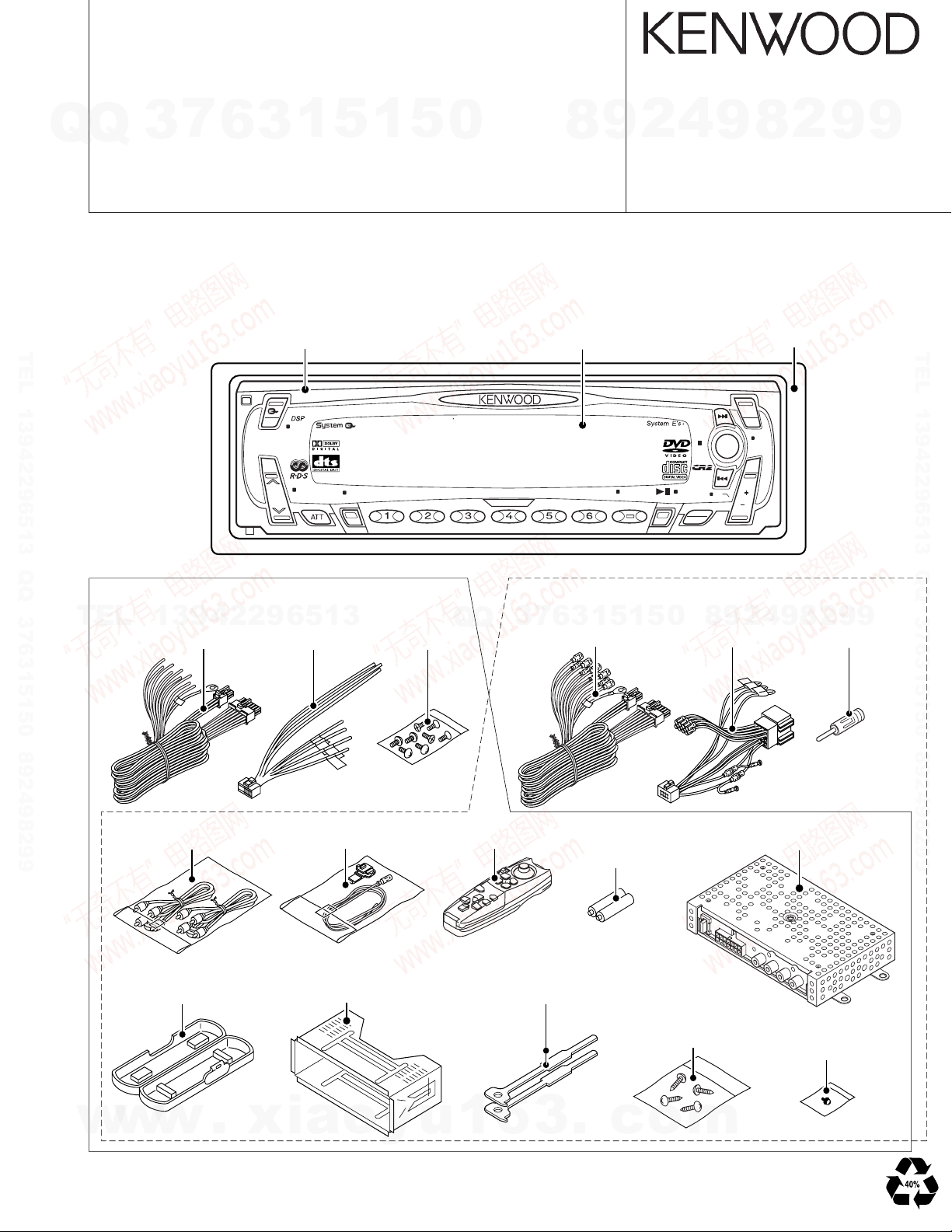
Front glass assy
(B10-4265-08) : Z920DVD
Panel assy
(A64-2753-08) : Z920DVD
TEL 13942296513 QQ 376315150 892498299
(A64-2754-08) : KDV-Z930/Z940/Z960
DISP
EX
NAME.S
SCAN RDM REP M.RDM TI
AUD
KDV-Z930
XOVER
(B10-4266-08) : KDV-Z930
(B10-4267-08) : KDV-Z940
(B10-4268-08) : KDV-Z960
CD MD-CH CONTROL DVD RECEIVER
8
4
2
9
© 2001-11 PRINTED IN JAPAN
B51-7862-00 (N) 2158
TIVOL ADJ
9
Escutcheon
(B07-3048-08) : Z920DVD
(B07-3059-08) : KDV-Z930/Z940/Z960
S.A
SRC
PWR
OFF
K3i
MENU
47Wx4
FM
NF
DISC
AM
8
3-D
DAB
2
9
9
TEL 13942296513 QQ 376315150 892498299
KDV-Z930/Z940/Z960 Z920DVD
TEL
13942296513
DC code assy
(E30-6095-08)
Connecting cord assy
(E30-6093-08)
Plastic cabinet assy
(A02-2711-08)
DC code assy
(E30-6097-08)
Connecting cord assy
(E30-4881-05)
Mounting hardware assy
(J21-9585-18)
Screw set
(N99-1723-05)
Q
Remote con. assy
(A70-2023-08)
3
Q
RC-DV200
Lever
(D10-4364-08)x2
7
5
1
3
6
DC code assy
(E30-6092-08)
Size AAA battery
(Not supplied)
0
5
1
DC code assy
(E30-6096-08)
Screw set
(N99-1726-08)
8
4
2
9
Cover
(F07-1112-08)
9
9
2
8
9
Antenna adaptor
(T90-0523-05)
Screw set
(N99-1716-08)
w
w
w
.
xia
o
y
u
1
6
3
.
c
o
m
KDV-Z930/Z940/Z960
2
Z920DVD
Q
ANT
TEL 13942296513 QQ 376315150 892498299
AUX-IN
DVD
CD-CH
DSP
Q
TUNER
E2P ROM
TEL
3
IC150
MAIN u-COM
RST MUTE IC
IC403
7
RDS
CD : 1300mV
CD-CH
13942296513
IC400
6
FM
: 255mV
AM : 190mV
: 1225mV
SW-OP
AMP
IC701
GND-ISO
3
: 1160mVAUX-IN
IC700
1
IC200 IC300
MUX
IC850
SA MIX
AMP
IC900
PANEL u-COM
5
FM : 1090mV
AM
CD
FRONT
E-VOL HPF
AC OUT
AN7399S
IC201
IC940
SA IC
: 680mV
: 2700mV
: 2650mVCD-CH
: 2650mVAUX
REAR
AC IN
1
IC202
MODE
IC961
5
SW
CONTROL BLOCK
IC950
ROM
IC930
REMO
KEY MATRIX
LEVEL SHIFT
0
Q
VFD
Q
AUXIN
(NF)
CD
CD-CH
AUX
AM
CD
CD-CH
AUX
: 1060mVFM
8
: 660mVAM
: 2660mV
: 2600mV
: 2600mV
FRONT
REAR
NF
: 520mVFM
: 320mV
: 1630mV
: 1530mV
: 1530mV
6
7
3
BU 5V
SW 5V
PNL 5V
AUDIO 8V
VFD
MECHA 7V
MECHA 5V
FUN 12V
AMP BLOCK-2
AUDIO 8V
3
9
AMP BLOCK-1
IC350
IC351
5
1
Q401
SW 5V
Q404
PNL 5V
Q602
AUDIO 8V
Q606
VFD 14V
Q611
MECHA 7V
IC750
MECHA 5V
Q610
FUN 12V
Q501
AUDIO 8V
2
GND-ISO
GND-ISO
5
1
0
4
Q613
9
IC500
POWER IC
9
8
2
8
4
FUSE 10A
FUSE 5ABU 5V
9
2
FRONT
REAR
NF
VIDEO OUT
DATA OUT
8
9
BU 14V
9
2
9
TEL 13942296513 QQ 376315150 892498299
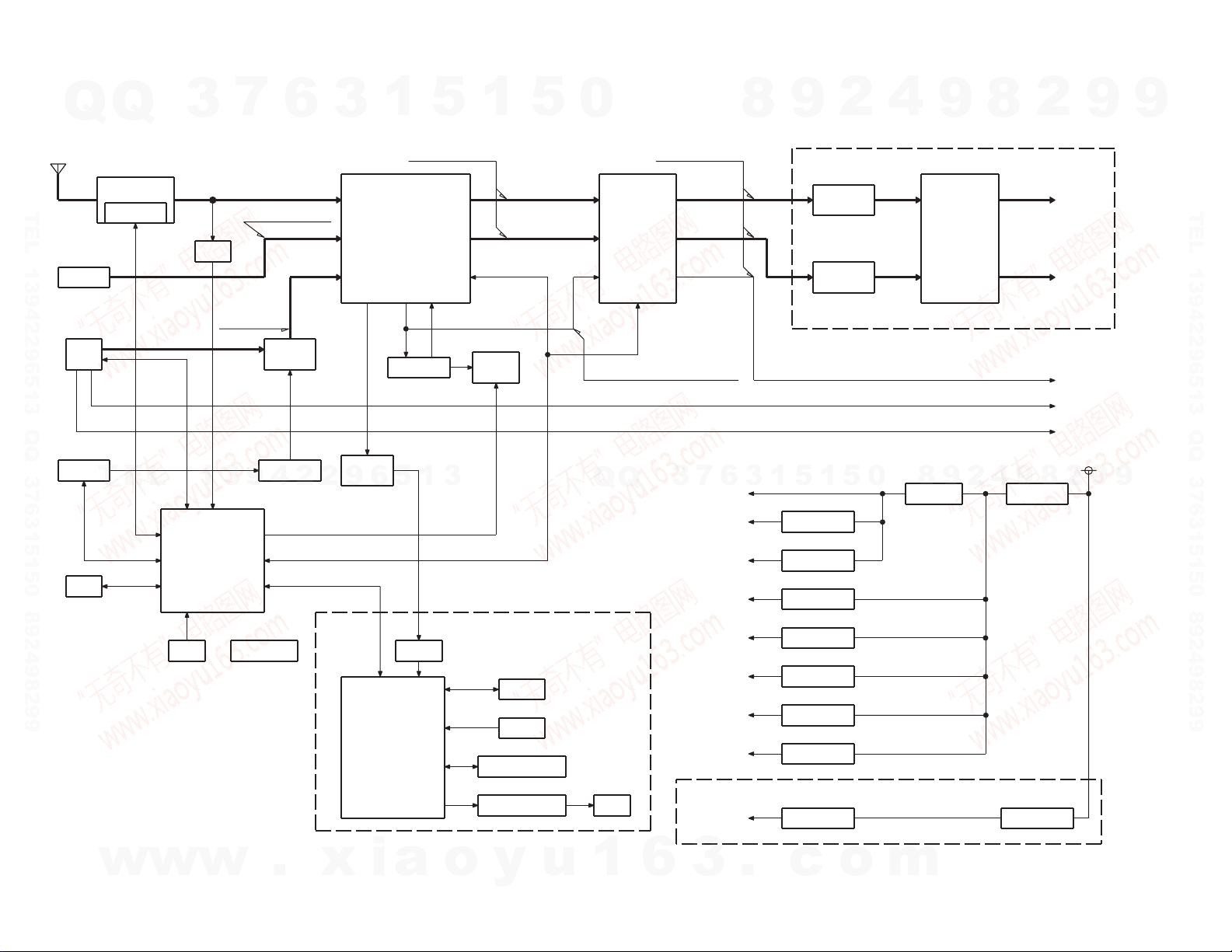
BLOCK DIAGRAM
9
w
w
w
.
x
i
a
o
y
u
1
6
3
.
c
o
m
KDV-Z930/Z940/Z960
COMPONENTS DESCRIPTION
Z920DVD
7
Q
Q
Ref.No. Element/Function Operation/Condition
IC150 RDS RDS DECODER
IC200 E-Vol/MPX E-Vol/MPX
IC201 SPATIALIZER
IC202 GATE IC GATE IC FOR SPATIALIZER
IC300 SYSTEM E'S SYSTEM E'S
IC350 GND-ISO GND-ISO FOR AMP
TEL 13942296513 QQ 376315150 892498299
IC351 GND-ISO GND-ISO FOR AMP
IC400 SYSTEM MI-COM
IC402 GATE IC GATE IC FOR MUTE
IC403 RESET SYSTEM RESET
IC500 POWER AMP
IC700 SW-OP CD/CD-CH SWITCHING INPUT
IC701 GND-ISO GND-ISO FOR CD-CH
IC750 5V REGULATOR
IC850 BUFF SA BUFF, 1/2Vdd
IC900 PNL MI-COM
IC930 REMOCON REMOTE CONTROL CENSOR
IC940 SA BPF BPF FOR SA
IC950
TEL
IC960
IC961 LEVEL SHIFT IC 5V-3.3V LEVEL SHIFT
Q100 FM+B SW
Q101 FM+B SW
Q102 AM+B SW
Q103 AM+B SW
Q104 EMI FIL
Q105 BUFF IFC BUFF
Q200 SURROUND SW SURROUND SW
Q201 SURROUND SW SURROUND SW
Q202 MUTE E-VOL MUTE SW
Q250 NOISE AMP FM NOISE AMP
Q350A
Q350B
Q351A
Q351B
Q352A
Q352B
Q353 MUTE DRV MUTE FOR PRE-OUT
Q400 MUTE DRV FOR SA MUTE
Q401 5V SW
Q402 LED SW LED SW FOR DISC IN,EJ-SW
w
Q403 LED SW LED SW FOR DSI
Q404 PNL5V SW
3
EXTENSION ROM
13942296513
3.3V POWER SUPPLY IC
MUTE DRV MUTE FOR PRE-OUT
MUTE DRV MUTE FOR PRE-OUT
MUTE DRV MUTE FOR PRE-OUT
MUTE DRV MUTE FOR PRE-OUT
MUTE DRV MUTE FOR PRE-OUT
MUTE DRV MUTE FOR PRE-OUT
w
w
6
5V FOR MECHANISM POWER SUPPLY
3.3V POWER SUPPLY
.
xia
3
1
5
o
1
y
5
u
0
Q
Q
1
Ref.No. Element/Function Operation/Condition
Q405 PNL5V SW
Q406 MUTE DRV PRE-OUT, DSP MUTE
Q501 GND-ISO 8V AVR 8V POWER SUPPLY FOR GND-ISO
Q502 14V SW 8V POWER SUPPLY FOR GND-ISO
Q503 14V SW 8V POWER SUPPLY FOR GND-ISO
Q504 AMP MUTE DRV MUTE FOR POWER AMP
Q505 AMP MUTE DRV MUTE FOR POWER AMP
Q600 14V SW AUDIO8V
Q601 14V SW AUDIO8V
Q602 AUDIO8V AVR 8V POWER SUPPLY FOR AUDIO
Q603 AUDIO8V AVR 8V POWER SUPPLY FOR AUDIO
Q604 DD-CONV SW
Q605 DD-CONV SW
Q606 DD-CONV AVR
Q607 DD-CONV AVR
Q608 14V SW MECHANISM 7V
Q609 14V SW MECHANISM 7V
Q610 FAN12V A VR FAN12V
Q611 MECHA7V AVR
7
3
Q612 MECHA7V AVR
Q613 BU5V AVR 5V POWER SUPPLY FOR MI-COM
Q614 BU5V AVR 5V POWER SUPPLY FOR MI-COM
Q615 14V SW FAN12V
Q616 14V SW FAN12V
Q650
Q651 DIMMER SW
Q652 P-CON SW
Q653 P-CON SW
Q654
Q655
Q658 ACC DET ACC ON/OFF DETECTION
Q659 BU DET BU ON/OFF DETECTION
Q660 PARKING SW
Q700 CD/CD-CH SW CD/CD-CH SIGNAL SWITCHING
Q701 BUFF DIGITAL BUFF
Q850 ALC ALC
Q851 MUTE DRV FOR SA MUTE
Q900 LED SW
Q930 PNL5V SW
Q931 PNL5V SW
Q960 BK SW
6
3
Q961 VFD SW
Q962 VFD SW
2
9
8
5
1
5
1
3
6
EXT AMP CON SW
P-CON PROTECTION
P-CON PROTECTION
.
c
o
4
9
14V POWER SUPPLY FOR DC/DC CONVERTER
14V POWER SUPPLY FOR DC/DC CONVERTER
7V POWER SUPPLY FOR MECHANISM
0
7V POWER SUPPLY FOR MECHANISM
LED SW FOR SRC,KENWOOD LOGO
PANEL 5V SW FOR SA-BPF,REMOCON
PANEL 5V SW FOR SA-BPF,REMOCON
8
9
2
8
4
2
9
8
9
2
9
9
9
m
TEL 13942296513 QQ 376315150 892498299
3
KDV-Z930/Z940/Z960
Z920DVD
MICROCOMPUTER’S TERMINAL DESCRIPTION
7
Q
Q
System microcomputer MN101C49KWA (IC400 : MAIN UNIT)
Pin Name Signal Name I/O Purpose Processing/Operation
1 VREF- VREF- - Connected to GND
2 PA0/AN0 PHONE I Phone input terminal Below 1 V : Phone Muted. Above
3 PA1/AN1 NOISE I FM noise detecion input terminal Threshold being checked. (Variable
4 PA2/AN2 S-METER I S-meter input from FM tuner
5 PA3/AN3 DISC-DET I
TEL 13942296513 QQ 376315150 892498299
6 PA4/AN4 NO_USE I Pulled down by a resistor
7 PA5/AN5 NO_USE I Connected to GND
8 PA6/AN6 NO_USE I Connected to GND
9 PA7/AN7 NO_USE I Connected to GND
10 VREF+ VREF+ - Connected to REF-CON
11 VDD VDD - Connected to BU 5 V
12 OSC2 X'TAL O Connected to X'tal (8.388608 MHz)
13 OSC1 X'TAL I Connected to X'tal (8.388608 MHz)
14 VSS VSS - Connected to GND
15 XI X'TAL I Connected to X'tal (32.768 KHz)
16 XO X'TAL O Connected to X'tal (32.768 KHz)
17 MMOD GND I Connected to GND
18 P00/SBO0/TXD0 PN-MC-DATA I/O Data output to Panel uCOM
19 P01/SBI0/RXD0 PN-SC-DATA I Data input from Panel uCOM
20 P02/SBT0 PN-MC-CLK O Clock output to Panel uCOM
TEL
21 P03/SBO2 DVD-D-FM O Data output to DVD uCOM
22 P04/SBI2 DVD-D-HOST I Data input from DVD uCOM
23 P05/SBT2 DVD-CLK I Clock input from DVD uCOM
24 P06/NDK/BUZZER BEEP O Beep output (2 KHz)
25 P07/SYSCLK NO_USE O Open
26 P20/IRQ0 BU-DET I BU detection input Lo : BU detected.
27 P21/IRQ1/ACZ RDS-CLK I Clock input from RDS
28 P22/IRQ2 CH-REQC I REQ input from CD-CH
29 P23/IRQ3 DVD-ATN-HOST I Connected to DVD-CLK
30 P24/IRQ4 DSP-REQD I REQ input from DSP
31 P25/IRQ5 PN-SC-REQ I REQ input from panel uCOM
32 P26 NO_USE O Connected to GND
33 P27/NRST RESET I System reset input Lo : REST
34 P10/TM0IO/RMOUT FUN_ON O Fun power control output
35 P11/TM1IO ANT-CON O Power antenna control output Hi : POW_ANT output = Hi.
36 P12/TM2IO EXT-AMP O External amp control output
37 P13/TM3IO DIMMER I Dimmer input Lo : DIMMER = ON
38 P14/TM7IO P-CON O External amp ON/OFF control output Hi : P_CON output = Hi.
39 P15 ACC-DET I Acc detection input Lo : Acc detected.
40 P16/TM4IO PARKING-DET I Parking detection input Hi : Parking detected.
41 P17 NO_USE O Open
42 P30/SBO1/TXD1 CH-DATAH O Data output to CD-CH
43 P31/SBI1/RXD1 CH-DATAC I Data input from CD-CH
44 P32/SBT1 CH-CLK O Clock output to CD-CH
45
w
46 P34/SBI3/NBT DSP-DATAD I Data input from DSP
47
3
13942296513
P33/SBO3/SDA/NBR
w
w
P35/SBT3/SCL/NLDDMA
6
DSP-DATAH O Data output to DSP
.
xia
DSP-CLK O Clock output to DSP
3
1
5
o
1
5
0
Disc sensor input. Analog detection 2.5 V
7
3
Q
Q
y
u
1
6
3
6
8
3
.
4
2
9
2.5 V : Navigation Muted.
depending on mode)
Hi : Disc detected. Lo : Disc not present.
8
0
5
1
5
1
Hi : Power ON (Same operation as DVD+B).
c
o
m
9
9
8
2
4
9
2
8
9
2
9
9
TEL 13942296513 QQ 376315150 892498299
9
4
KDV-Z930/Z940/Z960
Z920DVD
MICROCOMPUTER’S TERMINAL DESCRIPTION
7
Q
Q
TEL 13942296513 QQ 376315150 892498299
TEL
w
3
Pin Name Signal Name I/O Purpose Processing/Operation
48 P36/NSTDMA NO_USE O Open
49 P37/NDKDMA NO_USE O Open
50 P40/KEY0 TYPE0 I Destination type selection input
51 P41/KEY1 TYPE1 I Destination type selection input
52 P42/KEY2 ST-TYPE0 I EVOL control selection input
53 P43/KEY3 ST-TYPE1 I EVOL control selection input
54 P44/KEY4 RE-TYPE0 I Region code selection input
55 P45/KEY5 RE-TYPE1 I Region code selection input
56 P46/KEY6 DSP-CON O DSP control output Hi : DSP = ON
57 P47/KEY7 DSP-REQH O REQ output to DSP
58 P50/NWE DSP-RST O Reset output to DSP Hi : RESET
59 P51/NRE CH-RST O Reset output to CD-CH Hi : RESET
60 P52/NCS CH-MUTE I Muting signal input from CD-CH Hi : MUTE
61 P53/A16 CH-CON O CD-CH control output Hi : CD-CH = ON
62 P54/A17 CH-REQH O REQ output to CD-CH
63 P60/A0 NO_USE O Open
64 P61/A1 DVD/CH-SELECT O DVD/CD-CH audio selection output
65 P62/A2 DVD-+B O DVD power ON/OFF control output Hi : DVD power ON.
66 P63/A3 P-ON O Internal power control output Hi : Power ON.
67 P64/A4 P-MUTE O Muting output to internal amp
68 P65/A5 SVR O Ripple discharge circuit control output Hi : Discharged.
69 P66/A6 STBY O Internal amp standby control output Hi : Standby OFF (Power ON). Set
70 P67/A7 MODE0 O Surround mode switching output
71 P70/A8 MUTE O Muting output Hi : MUTE = ON
72 P71/A9 EVOL-CLK O Clock output to EVOL
73 P72/A10 EVOL-DATA I/O Data output to EVOL
74 P73/A11 SPATIALIZER O Spatializer ON/OFF control output Hi : SPATIALIZER = ON
75 P74/A12 MODE1 O Surround mode switching output
76 P75/A13 DVD-ATN-FM O ATN output to DVD uCOM
77 P76/A14 DVD-RDY-FM O Ready output to DVD uCOM
78 P77/A15 DVD-RST O Reset output to DVD uCOM Lo : RESET
79 P80/D0/LED0 PLL-CLK O Clock output to front end
80 P81/D1/LED1 PLL-DATA I/O Data output to front end
81 P82/D2/LED2 FM+B O FM power control Hi : FM power ON.
82 P83/D3/LED3 AM+B O AM power control Hi : AM power ON.
83 P84/D4/LED4 AFC O Output for time constant switching
84 P85/D5/LED5 IFC I IFC input from F/E
85 P86/D6/LED6 D-MUTE I Muting input from DVD uCOM
86 P87/D7/LED7 PRE-MUTE O Dual zone muting output Lo : MUTE = ON
87 PD0/SDO0 RDS-QUAL I QUAL input from RDS
88 PD1/SDO1 RDS-DATA I Data input from RDS
89 PD2/SDO2 LED_SW O Illumination output to subpanel Hi : Lamp ON.
90 PD3/SDO3 EJECT I EJECT switch input Lo : EJECT_SW ON.
91 PD4/SDO4
92 PD5/SDO5 PN-RST O Reset output to panel uCOM Lo : Reset.
13942296513
w
w
6
.
xia
1
3
PN-MC-REQ/PN-DET
5
o
1
5
0
7
3
Q
Q
when noise is detected
(EJECT_ button and disc insertion slot)
I/O REQ output to Panel uCOM/Panel Output : Communicating with panel
y
u
1
6
release detection input
3
6
8
3
.
9
1
1
5
c
4
2
Refer to the Destination Type Setting Table.
Refer to the Destination Type Setting Table.
Refer to the Destination Type Setting Table.
Refer to the Destination Type Setting Table.
Refer to the Destination Type Setting Table.
Refer to the Destination Type Setting Table.
Hi : DVD. Lo : CD-CH. Switched during muting.
Lo : Muting ON. Lo is output in momentary power down.
0
5
preliminarily to the same timing as P_ON.
Refer to the Destination Type Setting Table.
Refer to the Destination Type Setting Table.
Hi : Larger time constant (during reception).
Lo : Smaller time constant (during AF search).
o
uCOM. Input : Lo when panel is detected.
9
9
8
m
2
8
4
2
9
8
9
2
9
9
TEL 13942296513 QQ 376315150 892498299
9
5
KDV-Z930/Z940/Z960
Z920DVD
MICROCOMPUTER’S TERMINAL DESCRIPTION
7
Q
Q
Pin Name Signal Name I/O Purpose Processing/Operation
93 PD6/SDO6 PN-OPEN I Panel open/close detection input Lo : Panel open.
94 PD7/SDO7 DSI O Security lamp output Hi : Lamp ON. The lamp blinks when
95 DAVSS AVSS - Connected to GND
96 PC0/DA0 PAN5V O Panel 5 V power control output
97 PC1/DA1 SW5V O SW 5 V power control output Lo : Switching 5 V power ON.
TEL 13942296513 QQ 376315150 892498299
98 PC2/DA2 ILL-ON/PN-SC-CON O Button illumination control output/ Hi : Illumination ON, panel uCOM
99 PC3/DA3 REF-CON O VREF control output
100 DAVDD AVDD - Connected to BU 5 V
Destination Type Setting Table
TEL
Spatializer Setting Table
3
Destination M Hi Lo Lo Hi
13942296513
SPATIALIZER LOW Hi Hi Hi
6
1
5
1
3
Pin No. 50 51 54 55
Pin Name TYPE0 TYPE1 RE-TYPE0 RE-TYPE1
JLo Lo
KLo Hi
XHi Lo Hi Lo
CHi Lo Hi Hi
EHi Hi
Pin No. 74 70 75
Pin Name SPATIALIZER MODE0 MODE1
OFF Lo Lo Lo
BYPASS Lo Lo Lo
MID Hi Lo Hi
HIGH Hi Hi Lo
5
0
Panel uCOM control output control output = Hi.
7
3
Q
Q
6
8
3
4
2
9
the panel is released.
Hi : Panel 5 V power ON. "Lo" is output when the
panel is released or during momentary power down.
Hi is output in an interlocked operation with P_ON.
0
5
1
5
1
9
8
9
2
8
4
2
9
8
2
9
9
9
TEL 13942296513 QQ 376315150 892498299
9
IC2-4 Change Value Setting Table
Pin No. 52 53
Pin Name ST-TYPE0 ST-TYPE1
Initial value Lo Lo
IC2-4 Change 1 Lo Hi
Change 2 Hi Lo
Change 3 Hi Hi
Panel Microcomputer UPD703033GC097 (IC900 : Control uCOM)
PinNo.
1 VFD_DATA1 O Data output "1" to VFD driver
2 VFD_CLK O Clock output to VFD driver
3 NC I Resistor connected to GND
4 VFD_DATA2 O Data output "2" to VFD driver
5 VFD_CLK_IN I
6 EVdd Connected to PNL 5 V
7 EVss Connected to GND
w
8 NC O Output open.
9 5V_ON O
6
Pin name I/O Description Processing Operation
Clock input from VFD_CLK (For use in synchronization of DATA 1 and 2)
w
w
.
xia
o
y
u
1
Power supply control output to Remote Control IC and SA_IC.
6
3
.
c
o
m
5V ON : HI, 5V OFF : LO
KDV-Z930/Z940/Z960
Z920DVD
MICROCOMPUTER’S TERMINAL DESCRIPTION
7
Q
Q
PinNo.
14~16 A13~A15 O Address output "A13" ~ "A15" to external ROM
TEL 13942296513 QQ 376315150 892498299
20~26 A6~A12 O Address output "A6" ~ "A12" to external ROM
27~30 A1~A4 O Address output "A1" ~ "A4" to external ROM
35, 36 X2, X1 Connected to Main X'tal
40~42 NC O OUTPUT OPEN
45, 46 NC O OUTPUT OPEN
47~54 AD0~AD7 I Data input "AD0" ~ "AD7" from external ROM
TEL
57~64 AD8~AD15 I Data input "AD8" ~ "AD15" from external ROM
65~68 A16~A19 O Address output "A16" ~ "A19" to external ROM
81~85 KR5~KR1 I Key return "5" ~ "1"
94~96 KS3~KS1 O Key scan "3" ~ "1" and Flash uCOM write port
w
3
Pin name I/O Description Processing Operation
10 REMO I Remote control signal input
11 NC O Output open.
12 VFD_LATCH O Latch output to VFD driver
13 VFD_GCP O Luminance gradation control output to VFD driver
17 VFD_BLK O Blank output to VFD driver
18 IC/Vpp Test
19 A5 O Address output "A5" to external ROM
31 RESET I Reset input
32 XT1 Resistor connected to GND
33 XT2 OPEN
34 REGC 1 uF connected to GND
37 Vss Connected to GND
38 Vdd Connected to PNL 5 V
39 CLKOUT OPEN
43 OE O Output Enable output to external ROM
44 CE O Chip Enable output to external ROM
55 BVdd Connected to PNL 5 V
56 BVss Connected to GND
69 NC O OUTPUT OPEN
70 A21 O Address output "A21" to external ROM
71 AVdd Connected to PNL 5 V
72 AVss Connected to GND
73 AVref
74 SA_F01 I Spectrum analyzer signal input (63Hz)
75 SA_F02 I Spectrum analyzer signal input (150Hz)
76 SA_F03 I Spectrum analyzer signal input (330Hz)
77 SA_F04 I Spectrum analyzer signal input (1KHz)
78 SA_F05 I Spectrum analyzer signal input (3.3KHz)
79 SA_F06 I Spectrum analyzer signal input (10KHz)
80 LEVEL_M I MIX signal input for level meter
86 PN_SC_REQ O Send request output to Main uCOM
87 AVCONT O A/D reference voltage control output Operating : High.
88 PN_SC_CON I Operation control input from Main uCOM Operating : High. (Interrupt input)
89 NC O Output open.
90 SOURCE I SRC key input
91 BLUE O Blue LED control output LED ON : HI, LED OFF : LO
92 PN_MC_REQ I Send request input from Main uCOM
93 KS4 O Key scan "4"
97 PN_SC_DATA I Data input from Main uCOM
98 PN_MC_DATA O Data output to Main uCOM
99 PN_MC_CLK I Clock input from Main uCOM
100 NC I Resistor connected to GND
13942296513
w
w
6
.
xia
3
1
5
o
1
y
5
u
0
Q
Q
1
3
6
7
3
6
8
3
.
9
1
1
5
c
4
2
Display ON : High. Display OFF : Low.
0
5
ON : High. OFF : Low. (Interrupt input)
o
9
9
8
m
2
8
4
2
9
8
9
2
9
9
TEL 13942296513 QQ 376315150 892498299
9
7

KDV-Z930/Z940/Z960
Z920DVD
TEST MODE
7
Q
Q
1. How to enter the test mode
While holding the EQ and ATT keys, short press the SRC key
during ALL OFF mode.
2. How to exit from the test mode
Only reset the unit.
(Note) The test mode cannot be terminated by ACC OFF, power
OFF, momentary power down or panel detached.
3. Initial status in the test mode
• Sources : ALL OFF
• Display : All segments are lit.
• Volume : -10 dB (displayed as "30")
TEL 13942296513 QQ 376315150 892498299
• Loudness : OFF
• CRSC : OFF regardless of the presence of switching
• SYSTEM Q : Flat
4. Special display in Tuner mode
When any of the following messages is displayed in Tuner mode,
the F/E may be abnormal.
• "TNE2P NG" : The EEPROM is set to the default (unstable
values) because the F/E was shipped without passing through
the adjustment process, etc.
• "TNCON NG" : Communication with the F/E is not possible.
5. Forced switching of K3I
Each press of the Preset 6 key in Tuner mode should switch K3I
from AUT O Æ Forced Wide Æ Forced Middle Æ Forced Narrow
Æ AUTO.
The initial status is AUTO and the display shows these modes
TEL
as follows.
• AUTO : FMA
• Forced Wide : FMW
• Forced Middle : FMM
• Forced Narrow : FMN
6. Audio-related specifications
• A short press of the Q key initiates the audio adjustment mode.
• Continuous holding of a remote control key is inhibited.
• Bass, Middle and Treble are adjusted in 3 steps of Min / Flat /
Max with the Track Up/Down keys.
• Balance is adjusted in 3 steps of Left Max / CENTER / Right
Max with the Track Up/Down keys.
• Fader is adjusted in 3 steps of Rear Max / CENTER / Front
Max with the Track Up/Down keys.
• Bass f, Bass Q, Bass EXT, Middle f, Middle Q and Treble f are
not dealt with by the audio adjustment.
7. X'OVER-related specifications
• A short press of the ATT key initiates the X'OVER adjustment
mode.
• Continuous holding of a remote control key is inhibited.
• HPF is adjusted in 2 steps of Through/220Hz with the Track
Up/Down keys.
• LPF is adjusted in 2 steps of Through/120Hz with the Track
Up/Down keys.
8. Menu-related specifications
• A short press of the Track Up key during the ALL OFF mode
initiates the Menu mode.
• A short press of the S.A key except the ALL OFF mode initiates the Menu mode.
w
• Continuous holding of a remote control key is inhibited.
• Calendar adjustment and calendar display switching are eliminated from the Menu mode.
8
3
function.
13942296513
w
w
6
.
xia
3
1
5
o
1
y
5
u
0
9. Backup current measurement
When the unit is reset while ACC is OFF (i.e. by turning Backup
ON), the MUTE terminal goes OFF in 2 seconds in place of 15
second. (The DVD mechanism is not activated at this time.)
10. Special display when the display is all on
Pressing the Preset keys while the power is ALL OFF displays
the following information.
[PRESET 1] Version display (8 digits,
[PRESET 2] Serial No. display (8 digits)
[PRESET 3] Short press : View power ON time. (The All
[PRESET 4] Short press : Display DVD operation time.
[PRESET 5] Short press : Display DVD ejection count.
[PRESET 6] Short press : Display Panel open/close count.
7
3
Q
Q
11. Other specifications
• Messages such as "CODE OFF" are not displayed when
power is turned ON.
Security specifications
• Forced power ON mode (All models) Even when the security
mode is permitted, the power can be turned ON for only 30
minutes by pressing the SRC key while holding the ATT and
PRESET 4 keys depressed. After 30 minutes have elapsed,
the set can be restored only by resetting it.
• Method of security code registration after EEPROM (F/E) replacement (Code security models)
1. Enter the test mode. (See "(1) How to enter the test mode".)
2. Press the CLK key to enter the security registration mode.
3. Enter the code by pressing the PRESET 1/2/3/4 keys.
Example: To enter "3510"
• Press the PRESET 1 key 4 times.
• Press the PRESET 2 key 6 times.
• Press the PRESET 3 key 2 times.
• Press the PRESET 4 key once.
4. Press and hold the DISP key for 3 seconds until "AP-
PROVED" is displayed.
5. Exit from the test mode. (See "(2) How to exit from the test
mode".)
(Note) The security code of these models cannot be sub-
1
jected to the All Clear operation
6
3
4
2
9
8
Month/Day/Hour/Minute)
(Display) SYS xxxxxxxx System microcomputer
PAN xxxxxxxx Panel microcomputer
(Display) S. No. xxxxxxxx
(Note) S. No. FFFFFFFF : fixed in this model
OFF period is not counted.)
Long press/hold : Clear power ON time.
(Display) PonTim xxxxx Max. 65535 (hours)
Long press/hold : Clear DVD operation time
(Display) DVDTim xxxxx Max. 65535 (hours)
Long press/hold : Clear DVD ejection count.
(Display) EjeTim xxxxx Max. 65535 (times)
0
5
1
5
1
3
6
Long press/hold : Clear Panel open/close count.
(Display) PnCnt xxxxx Max. 655350 (times)
.
c
o
9
9
8
m
2
8
4
2
9
8
9
2
9
9
TEL 13942296513 QQ 376315150 892498299
9
A B C D E
F G H I
J
1
2
3
4
5
6
7
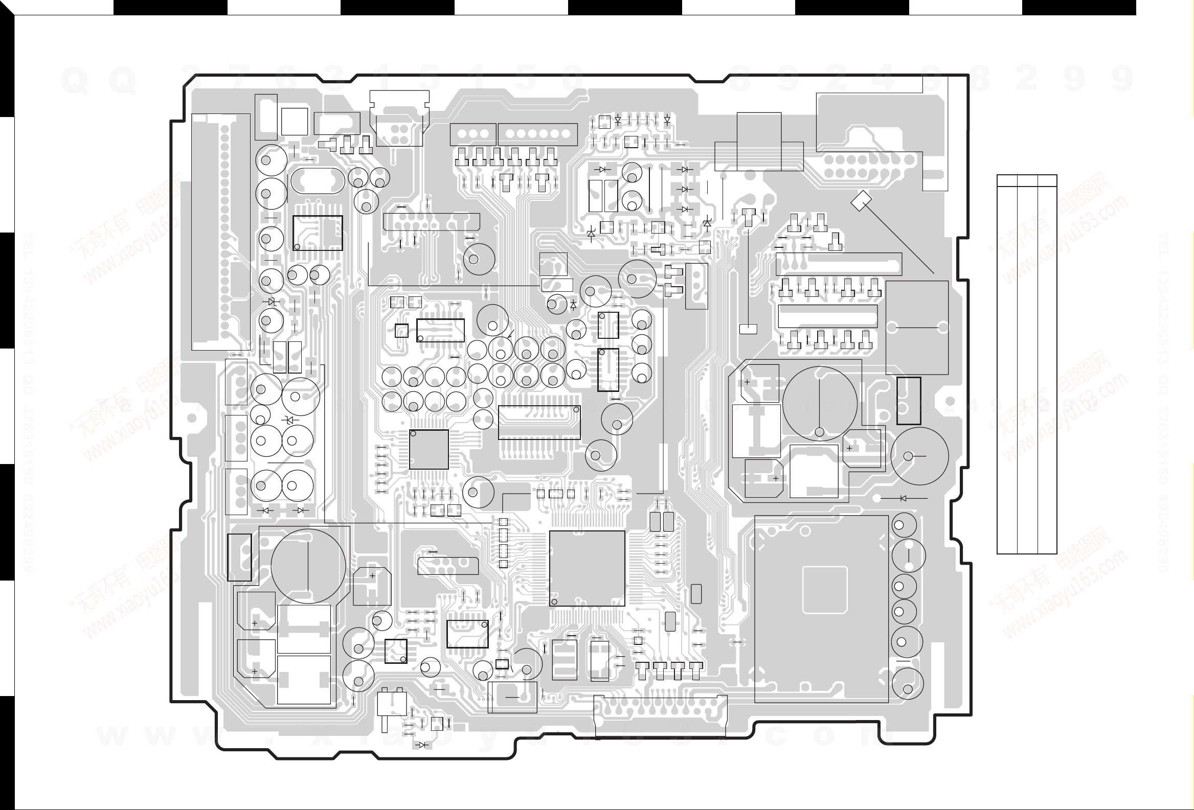
PC BOARD (COMPONENT SIDE VIEW)
C110
3
7
1
24
Q602
Q613
Q611
9
IC750
CN100
C104
L104
C108 C106
Q102
L106
C602
EBEBEB
4
C607
C606
D605
4
2
15
C752
C750
.
6
L100
C100
C102
16 9
L103
1
C151
D100
EB
EB
2
C609
R609
D606
L752
L102
L105
R104
D604
L750
3
1
D281
C111
X150
IC150
L150
Q100
L200
C600
2
C608
C611
x
Q
Q
3
TEL 13942296513 QQ 376315150 892498299
TU100
T
E
w
L
w
1
w
CN350
D282
8
C152
9
3
L751
C858
D280
C284
6
C852
R850
i
C203
C202
R200
R201
C204
C205
C753
1
C283
C201A
C201B
5
5
8
C851
S800
a
24
1
CN702
C282
R706
1
EB
85
14
BP
BP
IC850
5
3
CN700
C722
2
C720
C723
C724
Q201Q200
1
44
1
11
R851B
R851A
R855
4
1
R810
R40
EB
12
C206
C217
C214A
16 9
IC201IC202
18
C214B
C213
C211B
C210B
BP
BP
BP
BP
3
C211A
C200
34
11
IC200
23
22
C207
R203
R262
R202
EB
R263
Q250
R717
CN703
7
8
C850B
71
C850A
C853
814
C856
L400
C809
Q403
EB
R442
R811
o
D400
1
CN354
13 1 6
D350A
D350B
R352B
R352A
15
16
C721
C212A
BP
BP
C212B
BP
C307B
BP
C210A
C307A
C200
C209
BE
Q202
1
2
R709
R710
IC402
C410
y
C215
C419
D352A
D352B
R367B
C702
14
C408
43
12
C403
5
D351A
C351B
RN407
RN402
RN403
RN405
R427
R405
IC403
R407
CN351
D354B
R366A
Q610
C351A
C312B
u
R364B
C614
C312A
IC300
76
100
C404
D353A
CN600
E12B
C311B
RN400
RN406
75
1
R430
C412
0
D354A
R364A
C701A
C311A
R400
9
Q656
D658
C706
D602
C550A
1
Q
2815
RN401
IC400
X400
1
Q651
EB
C652
R655
R658
D655
EB
Q657
C703
14
17
Q
R411
R410
R401
X401
19
20
10
D651
R654
R656
EB
R653
Q650
C653
Q653
EB
EB
R670
R674
R677
R704
R705
85
IC701
148
IC700
R700
C305
C553
C580
51
50
26
25
R434
C407
C406
D804
6
R651
C661
C664
C700
RN404
R429
CN800
C650
R662
C655
Q658
D660
R443
C651
R652
EB
D701
C550B
C707
C701B
3
D650
R650
R657
D653
D654
R660
D656
R663
R659
R669
R675
C663
D700
7
R444
R420
R421
R422
R423
R676
D801D802
3
R668
Q660
EB
13
6
C414
R426
D800
1
2
R667
D657
CN701
.
8
D405
R440
CC2
3
C4
C810
MAIN UNIT
CC1
R515
0
L3
4
CN650
CN550
3
D553
D583
1
5
C2
m
2
4
8
D659
1
R807
9
CN651
132
4
R441
C552A
R551A
12 26 8 13 11 10 9 7 5 4 1
R510
R513
D550
13 11 10 9 7 5 4 1 2
CN580
R591
D580
C1
5
1
L1
41
DC800
58
c
2
16 9
8
D554A
D555
C554
C552B
R511
D581
D554B
R514
D552
R588
D582
L2
5
R551B
D551
R589
1
o
Refer to the schematic diagram for the values of resistors and capacitors.
9
IC1
9
C660
C613
L800
C808
C806
C803
C801
2
L650
8
4
2
MAIN UNIT
IC Q
150 3C
200 4D
201 3D
202 3D
300 4E
400 5F
402 6E
403 6E
700 4F
701 3F
750 5C
850 6D
100 4C
102 4C
200 3D
201 3D
202 5D
250 5D
8
9
403 7D
602 4C
610 3E
611 5C
613 4C
650 2F
651 2F
653 2F
656 2F
657 2F
658 2F
660 3G
Address
2
9
9
9
TEL 13942296513 QQ 376315150 892498299
9
 Loading...