Kenwood KDVS-210-P, KDVS-220-P, KDVS-230-P, KDVS-240-P Service manual
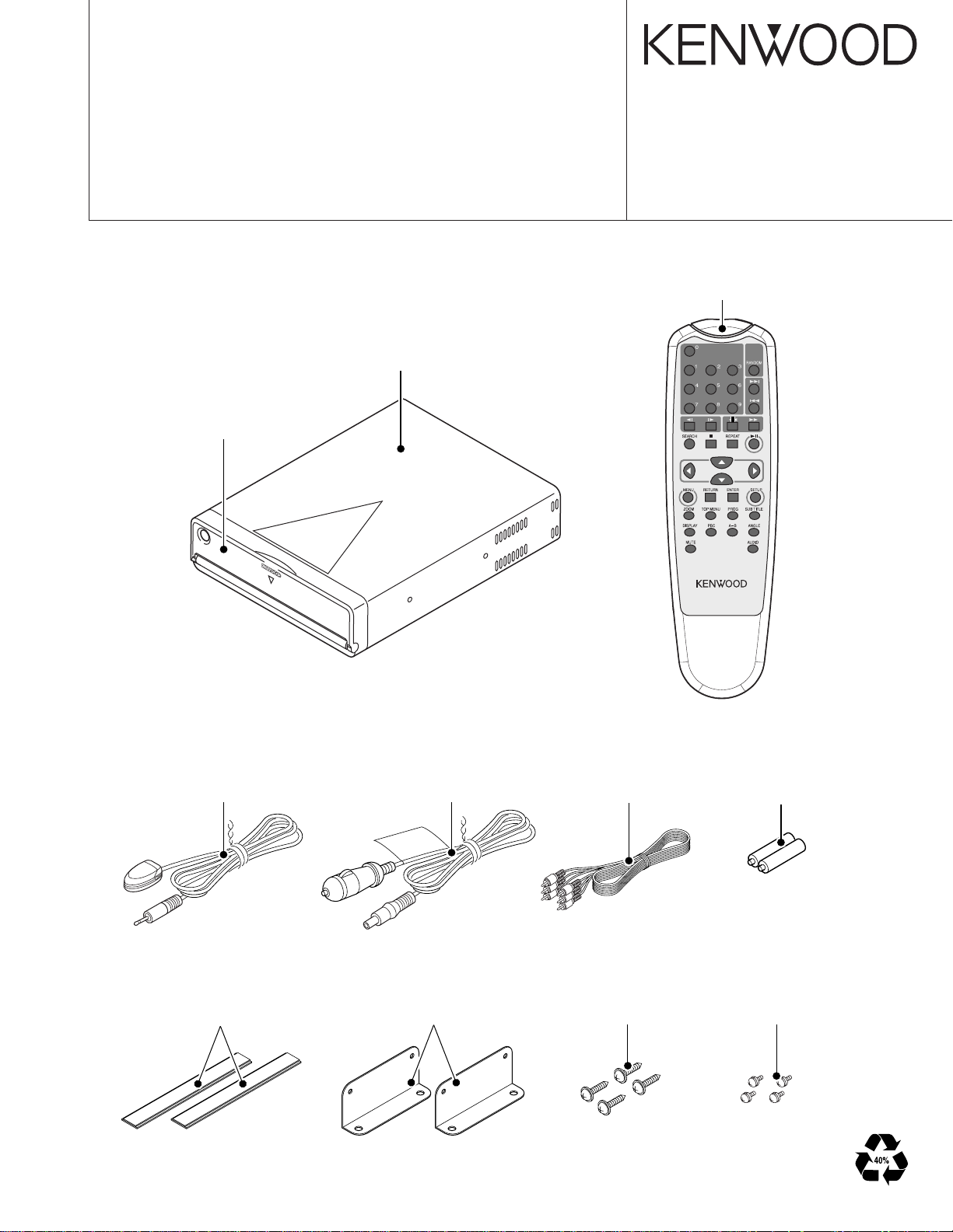
DVD PLAYER
KDV-S210P/S220P
/S230P/S240P
SERVICE MANUAL
Metallic cabinet
Panel assy
(A64-3526-08): KDV-S210P
(A64-3528-08): KDV-S220P
(A64-3529-08): KDV-S230P
(A64-3530-08): KDV-S240P
(A01-2845-08)
© 2004-5 PRINTED IN JAPAN
B53-0171-00 (N) 2703
Remote controller assy
(A70-2066-08)
Remote control sensor assy (6m)
(T95-0264-08)
Magic tape
(H30-0514-05)
x2
Cord with DC plug (2.4m)
(E03-0405-08)
Mounting hardware
(J22-0237-08)
x2
Cord with pinplug (3m)
(E30-6389-08)
Except KDV-S210P
Tapping screw
(N09-6274-08)
x4
RC-DV500
Size AAA battery
(Not supplied)
SEMS
(N09-6273-08)
x4
2
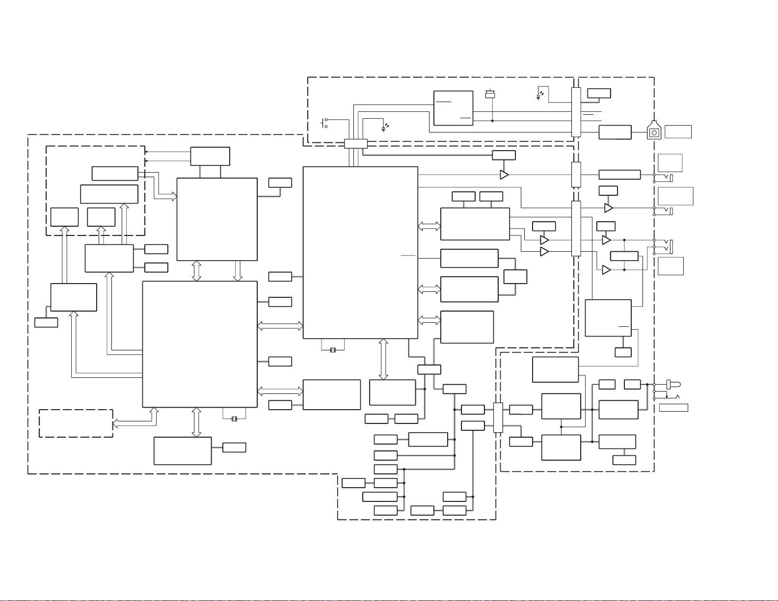
PROCESSOR
-DIGITAL SERVO CONTROL
DVD/CD DATA DECODING
SU6
SU1
SU3
MOTOR DRIVER
PWM
SU2
BTL
MOTOR DRIVER
HEAD AMPLIFIER
-GENERATING SERVO
-AUTO GAIN CONTROLLING
S+7V
MMVC
MVCC
DECODING & CORRECTING
-F/E CONTROL uP
-DATA BUFFERING
SVCC
-F/E PROGRAMING
FLASH MEMORY
3.3V
RFVCC
3.3V
VCC27
RFVCC
-DATA BUFFERING
DVD MPEG DECODING PROCESSOR
-MPEG DECODING
-B/E & SYSTEM CONTROL uP
U1
SU7
-B/E FRAME
SDRAM
-DVD/CD DATA
U34
CIRCUIT
LASER DRIVE
SQ4,5
U3
-F/E FRAME BUFFER
SDRAM 1Mx16BITS
-WORKING MEMORY
ACTUATOR &
BRUSHLESS
SY1
-F/E SYSTEM CLOCK
33.8688MHz
CERAMIC RESONATOR
CODE STORED
128kx8
-B/E SYSTEM CLOCK
CRYSTAL RESONATOR
27MHz
Y1
VCC27
-INCLUDING OVER
2ch AUDIO DAC
U35
DIGITAL FILTER
SAMPLING
U9
-RESETING
RESET IC
for U1
STORED
-SETUP & RESUME
EEPROM
INFORMATION
U2
U28
CODE STORED
-B/E PROGRAMING
FLASH ROM
VCC33
Q1
MMVC
MVCC
SVCC
3.3V
RFVCC
VCC33 AVCC
AVCC
RESET VCC
VCCA
S+7V
U5
REGULATOR
3.3V FIXED
SQ3
+7V
S7V
VCC
VCC
+7V
U23-1
U23-2
BUFFER
U27
POST LPF
-2nd ORDER
ACTIVE LPFx2
3.3V
CB5 CBP5
CBP7CB7
CB502 CBP502
CB3
CBD3
1MBITx8
BUFFER
4Mx16BITS
SERVO SIGNAL
RF AMPLITUDE
ERROR SIGNALS
INSERTION
DISC
SLIT
INDICATOR
EJECT SW
UD3
NAND GATES
POWER SW
INDICATOR
POWER
CBD1 CBP1
VCC
S7V
UP1
REGULATOR
SWITCHING
REGULATOR
SWITCHING
UP2
+B1
REGULATOR
5V
QP30
REGULATOR
QP40
28V
CIRCUIT
BU VCC
-GENERATING
TIMING
ON/OFF SW
DELAY CIRCUIT
VCC
RESET
REDUCING +B1
CIRCUIT
MUTE
-SENDING
DRIVING
-MUTE TR
+B1
ACTIVE LPFx2
LPF
-2nd ORDER
UP3-2
UP3-1
S7V
MUTE TR
QP4,5
UP4
VCC
75 Ohm
VIDEO
DRIVER
TRP1
PULSE TRANS
BU VCC
EYE INPUT
REMOTE
DC INPUT
ANALOG
OUT
AUDIO
VIDEO
OUT
COMPOSITE
DIGITAL
OUT
AUDIO
REMOTE
EYE
SPINDLE
MOTOR
to
SLEDGE
MOTOR
to
PICKUP HEAD
from SENSOR of
ACTUATOR COIL of
PICKUP HEAD
to
to CD LD
to DVD LD
+B
ERROR SIGNAL
INPUT
RF & SERVO
I/O
VPA
VM
PVCC
VCC
INTERFACE
COMMAND
DSP
CDLD DVDLD
DSP COMMAND
INTERFACE SIGNAL INPUT
RF & SERVO
CONTROL
LOADING
MECHANISM
OUTPUT
SERVO DRIVE SIGNAL
INTERFACE
FLUSH MEMORY
INTERFACE
SDRAM
AVDD5
INTERFACE
ATAPI
VDD 3.3
INTERFACE
SDRAM
INTERFACE
ATAPI
FLUSH MEMORY
EEPROM
RESET
DIGITAL AUDIO
VC25
INTERFACE
INTERFACE
INTERFACE
SPDIF OUT
SPDIF
UDAC
VIDEO DAC OUT
VC33
VCC
OUTPUT
SIGNAL
ERROR
RF & SERVO
RESET
HARDWARE
for F/E
INCLUDING
AUX4
AUX2
AUX7
VCC
VDD
VOUTR
VAA
VOUTL
VDD
ZRR
VCC
VCC
VCC
LED
RED
P DWN
P ON
+B DWN
LED
GREEN
IR
VSW
EN
VIN
VSW
EN
VIN
P ON
ZERO MUTE
VCC
V+ V+
CH-R
CH-L
VCC
+B DWN
P ON
IR
ZERO MUTE
SLOT-IN
LOADING MECHANISM
DISPLAY PCB POWER & OUTPUT PCB
COMBO PCB
TRAVERSE MECHANISM
KDV-S210P/S220P
/S230P/S240P
BLOCK DIAGRAM
KDV-S210P/S220P
/S230P/S240P
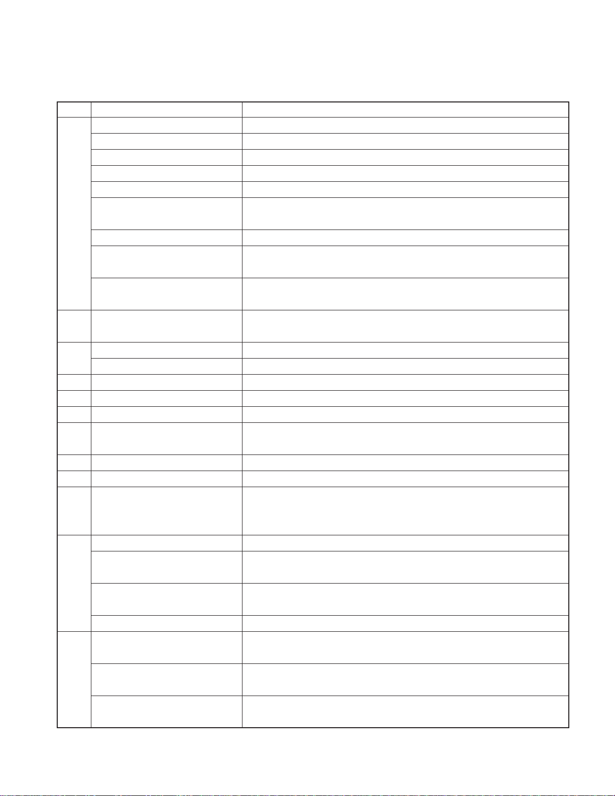
COMPONENTS DESCRIPTION
● COMBO PCB
Ref. No. Application / Function Operation / Condition / Compatibility
MPEG decoding control DVD MPEG images are decoded.
Dolby digital decoding control Outputs of Dolby digital audio are decoded.
LPCM audio decoding control LPCM audio of CD and DVD are decoded.
DVD navigation control DVD navigation is controlled.
ATAPI communication control ATAPI communication is control in order to control F/E.
U1
U2
U3
U5 3.3V regulator From No. 3 pin, VCC (5V) is input and from No. 2 pin, VCC33 (3.3V) is output.
U9 System reset control
U23 For audio post LPF CH1-side is Rch and CH2-side Lch. Constitutes a multiple feedback-type active LPF.
U27 SPDIF output, Pulse transformer driver
U28 B/E program memory Flash memory for storing B/E program memory.
U34 Program memory Flash memory for storing programs.
U35 Digital audio 2ch DAC
SU1
SU2 Feed motor driver
Built-in microcomputer for controlling
system and B/E system
Built-in video DAC Video DAC is built-in to output current for composite video output from No. 106 pin.
Digital audio DAC control output
Controls for keys and remote control
EEPROM for storing system setting
information and resume information
Frame buffer memory Decoding data buffer memory.
Program memory Memory for program control.
DVD/CD digital servo control Built-in DVD/CD digital servo equalizer and various timing generation circuit.
DVD/CD data decoding control
F/E section built-in system control
microcomputer
ATAPI communication control ATAPI communication control with B/E.
Pickup actuator driver
Motor driver for slot loading mechanism
System as a whole and B/E are controlled. 32bit RISC microcomputer is built-in.
Audio signals are output from No. 32 (TWS), 33 (TSD0), 39 (MCLK), and 40 (TBCK) pins. Also,
DAC system control is conducted using No. 160 (AUX0), 161 (AUX1), and 168 (AUX6) pins.
No. 162 pin is input for EJECT key. When receiving input, it is in L. No. 166 pin is for
remote control input. When receiving input, there will be pulse input.
EEPROM for storing system setting information and resume information.
Rising/Falling of VCC (5V) is detected by No. 5 pin, and L-reset output is made from No. 4 pin.
Inverters are connected in 3-step parallel connection for increased current capacity and
output to the pulse transformer.
Digital audio signal is input from No. 3 (TWS), 2 (TSD0), 16 (MCLK), and 1 (TBCK) pins.
Also, signals for DAC system control are input from No. 15 (AUX0), 14 (AUX1), and 13 (AUX6) pins.
Output for Lch analog audio is made from No. 7 pin and that for Rch is made from No. 8 pin.
Data generation from RF of DVD/CD, error correction and control over scramble analysis
and release.
F/E section 8bit microcomputer for system control.
Control signals for focus and tracking actuator signals of the pickup are received by No. 1 and
No. 26 pins respectively and currents are output from No. 13 and14 and No. 15 and 16 pins.
Control signals for the feed motor is received at No.6 pin and currents are output from
No. 11 and 12 pins.
Control signals for slot loading mechanism motor is received at No. 23 pin and currents
are output from No. 18 and 17 pins.
3

KDV-S210P/S220P
/S230P/S240P
COMPONENTS DESCRIPTION
Ref. No. Application / Function Operation / Condition / Compatibility
SU3
SU6 amplifier control
SU7
SU8
SQ3 3.3V regulator VCC (5V) is input from No. 3 pin and 3.3V is output from No. 2 pin.
SQ4 Driver for LD-driving for CD
SQ5 Driver for LD-driving for DVD
Spindle motor driver
Spindle motor rotation detection Rotation FG output for controlling spindle motor is output from No. 27 pin.
DVD/CD servo error signal replay
Built-in DVD/CD laser APC circuit Built-in LD current control circuit for DVD/CD.
Frame buffer memory Memory for temporarily caching read data of DVD/CD.
System memory External microcomputer memory for F/E system control.
CH1-side CH1-side
Servo reference voltage generation Signal after dividing VC25 (2.5V) into 2.1V enters the positive phase and output from the
amplifier output terminal as buffer output.
CH2-side CH2-side
RFRP (mirror detection signal) RF bottom hold signal and its DC are input to reverse input and positive input respectively
generation amplifier for canceling DC fluctuation. These then can be used as mirror signals.
Timing is controlled by No. 18 pin control signal for the 3-phase brushless spindle motor, using
No. 1~6 pins Hall element input signals, while current outputs are made from No 20, 22 and 24 pins.
Generation of various servo signals from pick up signals.
CD’s LD current control signals output from SU6 are received at base and the current
amount for LD driving is controlled.
DVD’s LD current control signals output from SU6 are received at base and the current
amount for LD driving is controlled.
● THERMISTER PCB
Ref. No. Application / Function Operation / Condition / Compatibility
UT1 Inverter
UT2 Comparator
QT1 Switching TR
THT1
Temperature detection thermister for
thermal shutdown
Output from UT2 comparator is inverted. Input is made on No. 2 pin and output on No. 4
pin. Activ e L.
Signal from thermister is inverse input and reference voltage is input to positive-phase
input. Output from thermister is comparated and output from No . 4 pin. Active H.
UT1 output is received on the base and output is inverted when it is made. The output is
feedback into the positive-phase input at UT2 for containing the fluctuations in outputs.
Resistance value is low at low temperature and high at high temper ature.
● DISPLAY PCB
Ref. No. Application / Function Operation / Condition / Compatibility
UD3
Power supply ON/OFF delay circuit With +B_DWN of reduced voltage detection circuit and OR of /P_ON signal, /P_DWN
NOR gate IC signal is generated.
● POWER & OUTPUT PCB
Ref. No. Application / Function Operation / Condition / Compatibility
UP1
VCC (+5V) generation switching Power supply is input from No. 2 pin and switching output is made from No. 3 pin.
regulator IC Going via choke coil, it becomes VCC (+5V) power supply output.
4
KDV-S210P/S220P
/S230P/S240P
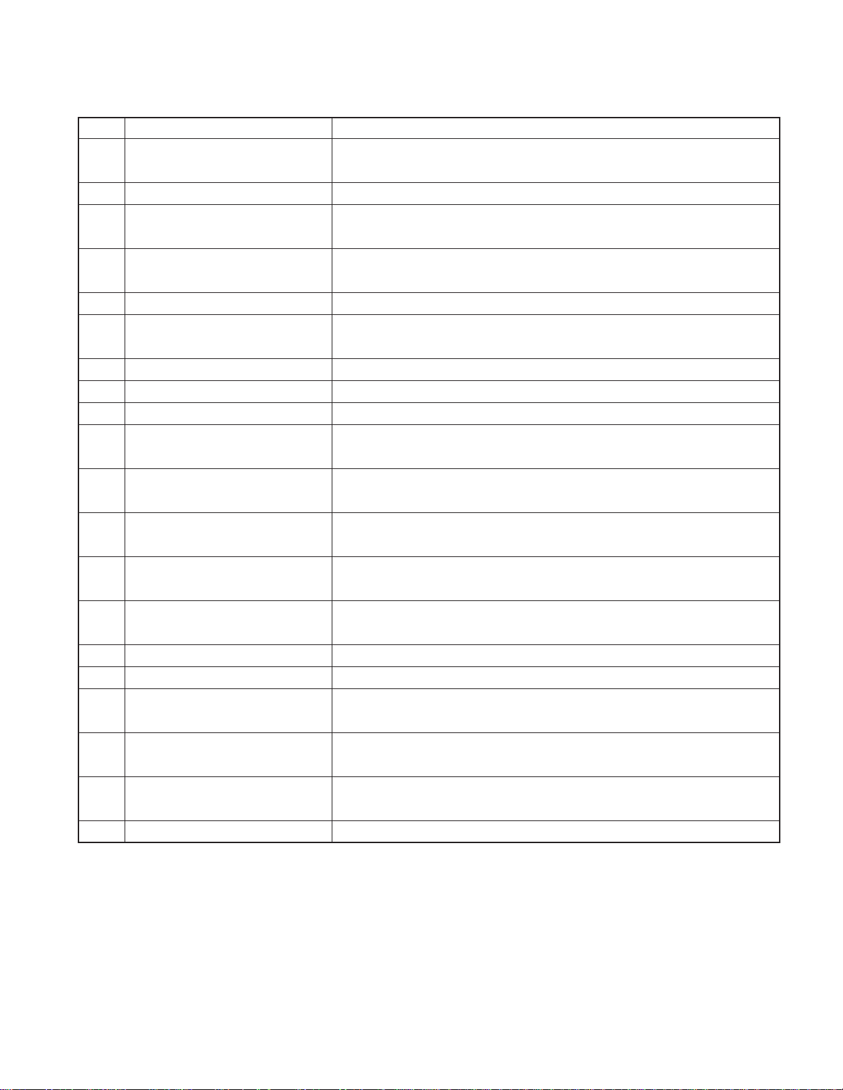
COMPONENTS DESCRIPTION
Ref. No. Application / Function Operation / Condition / Compatibility
UP2 S7V generation switching regulator IC
UP3 Analog audio output LPF amplifier CH1-side is Rch and CH2-side is Lch. Constitutes non-inverse active LPF composition.
UP4
QP1 Mute circuit driving TR
QP2 Mute circuit switching TR When this TR comes ON, muting is ON and when it comes OFF, muting is OFF.
QP3 Mute circuit switching TR
QP4 Rch mute TR When base is H, Rch is muted.
QP5 Lch mute TR When base is H, Lch is muted.
QP8 Composite video output buffer driver TR When the input signal comes in on the base, output is made from the emitter.
QP9
QP10 Mute circuit switching TR
QP11 Mute circuit switching TR
QP12
QP15
QP20
QP21
QP22
QP30 BU_VCC (+5V) regulator driving TR
QP40 28V regulator drive TR
QP41
Composite video output 75Ω driver
amplifier IC
Power supply ON/OFF delay circuit SW TR
Power supply ON/OFF delay circuit SW TR
Reduced voltage detection switching
TR for resume operation
Power supply ON/OFF delay circuit SW TR
Power supply ON/OFF delay circuit SW TR
Power supply ON/OFF delay circuit SW TR
TR for comprising Darlington connection
Power supply is input from No. 2 pin and switching output is made from No. 3 pin.
Going via choke coil, it becomes S7V power supply output.
Input is made on No. 3 pin and output is made from No 6 pin.
When QP2 is ON, input is made to the emitter. Mute circuit driving power supply is output
from the collector.
This is a TR for switching QP2. Therefore, the logic is inverted and when the TR comes
ON, muting is OFF, and when the TR comes OFF, the muting is ON.
When this TR is ON, base current of QP21 is shut off. QP21 is OFF and switching power
supply is ON.
When Z_MUTE signal in the base of this TR is active, (H on no signal), QP1 is turned ON
and the mute circuit is driven.
/P_ON in the base becomes L when the power switch comes ON. Therefore, it is H when
the power is OFF. When this happens, QP3 is forced to go OFF and muting is driven.
On the base of this TR, power switch triggered /P_ON signal comes in. When this is L, and QP22
is turned ON, base current of QP20 is shut off. When QP20 is OFF, switching power supply is ON.
At the time of reduced +B1, base current is shut off and the circuit goes OFF.
When this TR is ON, switching power supply is OFF.
When this TR is ON, switching power supply is OFF.
When this TR is ON, base current at QP20 is shut off. This means QP20 is OFF and
switching power supply is ON.
Receives batter power supply (+B1) by the collector and outputs regulation voltage 28V
(+B1) from the emitter.
Receives battery current (+B) with collector and outputs regulated voltage 28V (+B1) from the
emitter. This is used to counter the surge current, and it is normally about +B- +B1 =1.4V.
Along with QP40, constitutes Darlington connection and works to enhance compound hfe.
5
KDV-S210P/S220P
/S230P/S240P
MICROCOMPUTER’S TERMINAL DESCRIPTION
● B/E Microcomputer : ES6008 (COMBO PCB : U1)
Pin No. Pin Name I/O Application Processing Operation Description
1 VEE - I/O power supply (+3.3V) input
2~7 LA4~LA9 O Flash ROM address bus
8 VSS - Digital GND
9 VCC - Core power supply (+2.5V) input
10~16 LA10~LA16 O Flash ROM address bus
17 VSS - Digital GND
18 VEE - I/O power supply (+3.3V) input
19~21 LA17~LA19 O Flash ROM address bus
22,23 LA20,LA21 O Flash ROM address bus NC
24 /RESET I Chip reset input
25 TDMDX O NC
25 RSEL I ROM selection terminal Selected by 8bit ROM
26 VSS - Digital GND
27 VEE - I/O power supply (+3.3V) input
28 TDMDR I NC
29 TDMCLK I NC
30 TDMSF I NC
31 TDMTSC# O NC
32 TWS O Audio frame synchronization output
32 SEL_PLL2 I System and DSCK output clock selection [2] Selected by DCLK x 4
33 TSD0 O Audio serial data port 0
33 SEL_PLL0 I System and DSCK output clock selection [0] Selected by DCLK x 4
34 VSS - Digital GND
35 VCC - Core power supply (+2.5V) input
36 TSD1 O Audio serial data port 1 NC
36 SEL_PLL1 I System and DSCK output clock selection [1] Selected by DCLK x 4
37,38 TSD2,TSD3 O Audio serial data port 2,3 NC
39 MCLK O Audio master clock
40 TBCK O Audio bit clock output
41 SPDIF O SPDIF output
41 SEL_PLL3 I Clock source selection Selected by crystal oscillator
42 NC - NC
43 VSS - Digital GND
44 VCC - Core power supply (+2.5V) input
45 RSD I Audio input serial data NC
46 RWS I Audio input frame synch NC
47 RBCK I Audio input bit clock NC
48 NC - NC
49 XIN I Crystal input
6
KDV-S210P/S220P
/S230P/S240P
MICROCOMPUTER’S TERMINAL DESCRIPTION
Pin No. Pin Name I/O Application Processing Operation Description
50 XOUT O Crystal output
51 AVEE - PLL analog power source (+3.3V) input
52 VSS - Digital GND
53~58 DMA0~DMA5 O DRAM address bus [0]~[5]
59 VEE - I/O power supply (+3.3V) input
60 VSS - Digital GND
61~66 DMA6~DMA11 O DRAM address bus [6]~[11]
67 VSS - Digital GND
68 VEE - I/O power supply (+3.3V) input
69 /DCAS O DRAM Column address strobe
70 /DOE O DRAM output enable Not used.
70 DSCK_EN O DRAM clock enable
71 /DWE O DRAM write enable
72 /DRAS O DRAM low address strobe
73,74 DMBS0,DMBS1 O SDRAM bank select 0,1
75 VEE - I/O power supply (+3.3V) input
76 VSS - Digital GND
77~82 DB0~DB5 I/O DRAM data bus [0]~[5]
83 VCC - Core power supply (+2.5V) input
84 VSS - Digital GND
85~90 DB6~DB11 I/O DRAM data bus [6]~[11]
91 VSS - Digital GND
92 VEE - I/O power supply (+3.3V) input
93~96 DB12~DB15 I/O DRAM data bus [12]~[15]
97 /DCS1 O SDRAM chip select [1] NC
98 VSS - Digital GND
99 VEE - I/O power supply (+3.3V) input
100 /DCS0 O SDRAM chip select [0]
101 DQM O DATA input/output mask
102 DSCS O SDRAM clock output
103 VSS - Digital GND
104 VEE - I/O power supply (+3.3V) input
105 DCLK I PLL 27MHz clock input NC
106 YUV0 O YUV0 pixel output data Not used.
106 CAMIN2 I Camera input 2 Not used.
106 UDAC O U video DAC output Output for composite video out
107 YUV1 O YUV1 pixel output data Not used.
107 VREF I Video DAC reference voltage input
108 YUV2 O YUV2 pixel output data NC
108 CDAC O Video DAC output NC
7
KDV-S210P/S220P
/S230P/S240P
MICROCOMPUTER’S TERMINAL DESCRIPTION
Pin No. Pin Name I/O Application Processing Operation Description
109 YUV3 O YUV3 pixel output data Not used.
109 COMP I Compensation input
110 YUV4 O YUV4 pixel output data Not used.
110 RSET I DAC current adjust input
111 ADVEE - Video DAC analog power supply input
112 VSS - Digital GND
113 YUV5 O YUV5 pixel output data NC
113 YDAC O Y video DAC output NC
114 YUV6 O YUV6 pixel output data NC
114 VDAC O V video DAC output NC
115 YUV7 O YUV7 pixel output data NC
115 CAMIN3 I Camera YUV input 3 NC
116 PCLK2XSCN I/O 27MHz video output pixel clock NC
116 CAMIN4 I Camera YUV input 4 NC
117 PCLKQSCN O 13.5MHz video outout pixel clock NC
117 CAMIN5 I Camera YUV input 5 NC
118 /YSYNC I/O Vertical synchronization NC
118 CAMIN6 I Camera YUV input 6 NC
119 /HSYNC I/O Horizontal synchronization NC
119 CAMIN7 I Camera YUV input 7 NC
120 VSS - Digital GND
121 VCC - Core power supply (+2.5V) input
122 HD0 I/O Host data I/O [0] HD8
122 DCI [0] I/O DVD channel data I/O [0] Not used.
122 EAUX1 [0] I/O AUX1 data I/O [0] Not used.
123 HD1 I/O Host data I/O [1] HD9
123 DCI [1] I/O DVD channel data I/O [1] Not used.
123 EAUX1 [1] I/O AUX1 data I/O [1] Not used.
124 HD2 I/O Host data I/O [2] HD10
124 DCI [2] I/O DVD channel data I/O [2] Not used.
124 EAUX1 [2] I/O AUX1 data I/O [2] Not used.
125 HD3 I/O Host data I/O [3] HD11
125 DCI [3] I/O DVD channel data I/O [3] Not used.
125 EAUX1 [3] I/O AUX1 data I/O [3] Not used.
126 HD4 I/O Host data I/O [4] HD12
126 DCI [4] I/O DVD channel data I/O [4] Not used.
126 EAUX1 [4] I/O AUX1 data I/O [4] Not used.
127 HD5 I/O Host data I/O [5] HD13
127 DCI [5] I/O DVD channel data I/O [5] Not used.
127 EAUX1 [5] I/O AUX1 data I/O [5] Not used.
8

KDV-S210P/S220P
/S230P/S240P
MICROCOMPUTER’S TERMINAL DESCRIPTION
Pin No. Pin Name I/O Application Processing Operation Description
128 HD6 I/O Host data I/O [6] HD14
128 DCI [6] I/O DVD channel data I/O [6] Not used.
128 EAUX1 [6] I/O AUX1 data I/O [6] Not used.
129 VSS - Digital GND
130 VEE - I/O power supply (+3.3V) input
131 HD7 I/O Host data I/O [7] HD15
131 DCI [7] I/O DVD channel data I/O [7] Not used.
131 EAUX1 [7] I/O AUX1 data I/O [7] Not used.
131 VFD_DIN I VFD data input Not used.
132 HD8 I/O Host data I/O [8] HD0
132 /DCI_FDS I/O DVD input sector start Not used.
132 EAUX2 [0] I/O AUX2 data I/O [0] Not used.
132 VFD_CLK I VFD clock input Not used.
133 HD9 I/O Host data I/O [9] HD1
133 EAUX2 [1] I/O AUX2 data I/O [1] Not used.
133 SQSQ I Sub code Q data Not used.
134 HD10 I/O Host data I/O [10] HD2
134 EAUX2 [2] I/O AUX2 data I/O [2] Not used.
134 SQSK I Sub code Q clock Not used.
135 HD11 I/O Host data I/O [11] HD3
135 EAUX2 [3] I/O AUX2 data I/O [3] Not used.
135 IRQ O IRQ output Not used.
136 HD12 I/O Host data I/O [12] HD4
136 EAUX2 [4] I/O AUX2 data I/O [4] Not used.
136 C2PO I C2PO error correction flag input from CD-ROM Not used.
137 HD13 I/O Host data I/O [13] HD5
137 EAUX2 [5] I/O AUX2 data I/O [5] Not used.
137 SP I 16550 UART serial port input Not used.
138 VSS - Digital GND
139 VCC - Core power supply (+2.5V) input
140 HD14 I/O Host data I/O [14] HD6
140 EAUX2 [6] I/O AUX2 data I/O [6] Not used.
140 SQSI I Sub code Q synch Not used.
141 HD15 I/O Host data I/O [15] HD7
141 EAUX2 [7] I/O AUX2 data I/O [7] Not used.
141 IR I IR remote control input Not used.
142 /HWRQ O Host write request NC
142 /DCI_REQ O DVD control interface request NC
142 EAUX4 [0] I/O AUX4 data I/O 5 NC
143 /HRRQ O Host read request NC
9

KDV-S210P/S220P
/S230P/S240P
MICROCOMPUTER’S TERMINAL DESCRIPTION
Pin No. Pin Name I/O Application Processing Operation Description
143 EAUX4 [1] I/O AUX4 data I/O 4 NC
144 HIRQ I/O Host interrupt
144 /DCL_ERR I/O DVD channel data error Not used.
144 EAUX4 [0] I/O AUX4 data I/O 0 Not used.
145 /HRST O Host reset
145 EAUX3 [5] I/O AUX3 data I/O 5 Not used.
146 HIORDY I Host I/O ready
146 EAUX3 [3] I/O AUX3 data I/O 3 Not used.
147 VSS - Digital GND
148 VEE - I/O power supply (+3.3V) input
149 /HWR I/O Host write request
149 DCI_CLK I/O DVD channel data clock Not used.
149 EAUX4 [5] I/O AUX4 data I/O 5 Not used.
150 /HRD O Host read request
150 /DCI_ACK O DVD channel data valid Not used.
150 EAUX4 [6] I/O AUX4 data I/O 6 Not used.
151 /HIOCS16 I Device 16-bit data transfer
151 CAMCLK I Camera port pixel clock input Not used.
151 EAUX3 [4] I/O AUX3 data I/O 4 Not used.
152 /HCS1FX O Host select 1
152 EAUX3 [7] I/O AUX3 data I/O 7 Not used.
153 /HCS3FX O Host select 3
153 EAUX3 [6] I/O AUX3 data I/O 6 Not used.
154 HA0 I/O Host address bus 0
154 EAUX4 [2] I/O AUX4 data I/O 2 Not used.
155 HA1 I/O Host address bus 1
155 EAUX4 [3] I/O AUX4 data I/O 3 Not used.
156 VSS - Digital GND
157 VEE - I/O power supply (+3.3V) input
158 HA2 I/O Host address bus 2
158 EAUX4 [4] I/O AUX4 data I/O 4 Not used.
159 VEE - I/O power supply (+3.3V) input
160,161 AUX0,AUX1 I/O Accessory port 0,1 NC
162 AUX2 I Accessory port 2 EJECT key input
162 /IOW O I/O write strobe Not used.
163 VSS - Digital GND
164 VEE - I/O power supply (+3.3V) input
165 AUX3 I/O Accessory port 3 NC
165 /IOR O I/O read strobe NC
166 AUX4 I Accessory port 4 IR remote control input
10
KDV-S210P/S220P
/S230P/S240P
MICROCOMPUTER’S TERMINAL DESCRIPTION
Pin No. Pin Name I/O Application Processing Operation Description
167,168 AUX5,AUX6 I/O Accessory port 5,6 NC
169 AUX7 I Accessory port 7 Power down detection
170 /LOE O Device output enable
171 VSS - Digital GND
172 VCC - Core power supply (+2.5V) input
173~175 /LCS0~/LCS2 O Chip select 0~2 NC
176 /LCS3 O Chip select 3
177 VSS - Digital GND
178~182 LD0~LD4 I/O Flash ROM device data bus [0]~[4]
183 VEE - I/O power supply (+3.3V) input
184 VSS - Digital GND
185~191 LD5~LD11 I/O Flash ROM device data bus [5]~[11]
192 VSS - Digital GND
193 VEE - I/O power supply (+3.3V) input
194~197 LD12~LD15 I/O Flash ROM device data bus [12]~[15]
198 /LWRLL O Device low bite write enable NC
199 /LWRHL O Device high bite write enable NC
200 VSS - Digital GND
201 VEE - I/O power supply (+3.3V) input
202 CAMIN0 I Camera YUV0 NC
203 CAMIN1 I Camera YUV1 NC
204~207 LA0~LA3 O Flash ROM address bus
208 VSS - Digital GND
● F/E Microcomputer : M5705 (COMBO PCB : SU1)
Pin No. Pin Name I/O Application Processing Operation Description
1AVSS_DS - Data slicer port analog ground 2 XSRFIN I Analog RF signal input after passing through equalizer 3 XSIPIN I Data slicer inverse input 4AVDD5_DS - Data slicer port analog +5V power supply 5 XSDSSLV O Slice level output 6 XSRSLINT I Analog data slicer reference current setting input 7 VDD - Digital +3.3V power supply input 8 XSAWRC O Control putout for widening VCO range 9 XSRFGC O Loading motor control signal L : Eject, H : Loading, Vref : Stop
10 XSEFGC O NC 11 XSFOCUS O Focus actuator control DA output 12 XSTRACK O Tracking actuator control DA output 13 XSSLEG O Feed motor control DA output 14 AVDD5_DA - DAC analog +5V power supply input -
11
 Loading...