

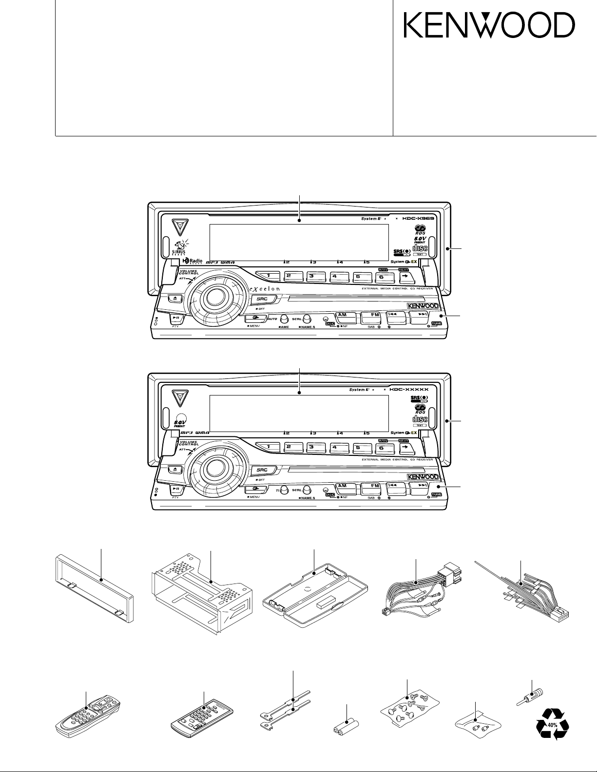
CD RECEIVER
KDC-9023R
KDC-PSW9524
KDC-X969
SERVICE MANUAL
© 2003-2 PRINTED IN JAPAN
B53-0031-00 (N) 3379
CD mechanism operation description is
not in this service manual.
Please, refer to service manual X924030-0x (B51-7867-00).
Panel assy
(A64-2982-01): KDC-9023R, (A64-2984-01):KDC-PSW9524
Panel assy
(A64-2975-01): KDC-X969
CD mechanism extension cord : W05-0935-00
50 4W
s
COMPACT
DIGITAL AUDIO
50 4W
s
COMPACT
DIGITAL AUDIO
Escutcheon
(B07-3079-01)
Panel assy
(A64-2993-02):
KDC-X969
Escutcheon
(B07-3079-01)
Escutcheon
(B07-3079-01)
Remote controller assy
(RC-505)
(A70-2040-05)
: KDC-X969
Mounting hardware assy
(J21-9823-03)
Remote controller assy
(RC-420)
(A70-2026-05)
: KDC-9023R/PSW9524
Plastic cabinet assy
(A02-2731-03)
Lever
(D10-4674-04) x 2
Size AA battery
(Not supplied)
DC cord (ISO)
(E30-4942-05)
: KDC-9023R/PSW9524
Screw set
(N99-1723-05)
: KDC-X969/9023R
Screw set
(N99-1734-05)
Panel assy
(A64-3002-02):
KDC-9023R/PSW9524
DC cord
(E30-6062-05)
: KDC-X969
Antenna adaptor
(T90-0552-05)
: KDC-9023R/PSW9524

KDC-9023R
/PSW9524/X969
HOW TO THE PANEL MECHANISM ASSEMBLY
1. Fixed the position of operation side
(Fixed the horizontal position when the panel opened)
q The mounting hardware (281) of operation side is rota-
tion (A) into the stop position with close side.
w As figure (B) line is just above and the gear (230) at-
tached to pin.
2. The slider assembly insert to bottom chassis
q The bracket for display panel (284) is leave down, in-
sert to the chassis (702). (C)
A
Rotary to the
stop position
B
This line attached just above
Fig. B
(This figure from look at B arrow)
284
281
230
w The slider assembly insert to the chassis (702) after
that shift (D) direction.
e The bracket for display panel (284) is raised (E) direc-
tion.
r Keep the raising conditions, the slider assembly is shift
(F) direction.
(Note) Do not bend the knob of chassis detection switch
when the slider assembly insert.
SW
C
702
284
F
E
SW
D
702
3
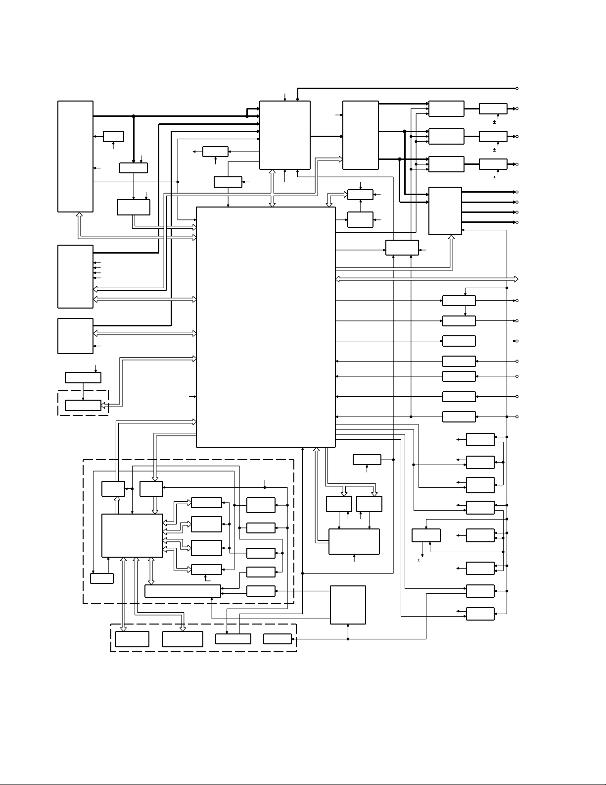
BLOCK DIAGRAM
KDC-9023R
/PSW9524/X969
(X25-964)
TUNER
AUDIO OUT
S-METER
CD
CH
Q501
EEP5V
IC1
EEPROM
TDF UNIT
(X16-208)
DISPLAY
UNIT
(X16-210)
SWITCH UNIT
(X16-217)
BU5V
REMO
IC9
Q303,304
AM+B
8V 8V
8V
IC14
BU5V
8V
SERVO
CD4.7V
BACK UP
IC7
LEVEL
SHIFT
IC11
ROT ARY
ENCODER
BUFFER
SW5V
RDS
DECODER
IC8
u-COM
LEVEL
SHIFT
BPF
BU5V
IC3
IC2
IC4
IC10
FL
KEY
KEY MATRIX
AGC
IC1
SRAM
MASK
ROM
FLASH
MEMORY
BPF
8V
BUFFER
AGC
RESET SW
SW5V
PANEL5
Q6,10
PANEL
SW5V
IC6
3.3V
Q5
SW3.3V
Q4
FL3.3V
Q2,3
FL+B
IC2
FM
AM
CD
CH
QUAL
u-COM
KEY ILL
8V
E-VOL
&
MPX
8V
IC15
MOTOR
FL+B
FAC
IC5
SYSTEM
E'S+
IC20
FOCUS
SW
IC8
SERVO
PANEL
MECHA
SW5V
DC/DC
WOW
RESET
IC16
MOTOR
DRDR
IC6
BU5V
IC9
8V
8V
MUTE
DRIVER
Q207,208
PRE MUTE
Q203,204
PRE MUTE
Q205,206
PRE MUTE
IC4
POWER
IC
BU5V
IC18
Q23,24
ANT-CON ANT CON
Q25
EXT AMP
Q26
DIMMER DIMMER
TEL MUTE
Q29
ACC DET
Q27
B.U DET
BU5V
SW5V
PANEL5V
SW14V
DC/DC A8V
9V
SERVO
CD4.7V
IC13
IC12
IC11
P-CON P CON
Q1,2
BU5V
Q3,601
SW 5V
Q502,503
PANEL
5V
Q4,5
SW 14V
Q6-8
A8V
Q9,602
SERVO
Q11-14
FL+B
IC19
SW REG
OP AMP
9V
OP AMP
9V
OP AMP
9V
AUX IN
PRE OUT
(NF)
PRE OUT
(REAR)
PRE OUT
(FRONT)
SP OUT (FL)
SP OUT (FR)
SP OUT (RL)
SP OUT (RR)
WIRED REMO/
OPEL DISP I/F
EXT.AMP.CON
TEL MUTE
ACC
BACK UP
3

KDC-9023R
/PSW9524/X969
BLOCK DIAGRAM
(X32-5440-00)
PICK-UP
A
EF
C
B
TR COIL
FO COIL
SPINDLE
MOTOR
LOADING &
SLED MOTOR
7
Q4
APC
MOTOR
DRIVER
D. GND
IC4
IC11
VREF
X1
CLOCK
16.93MHz
16.93MHz
S. GND
1 CHIP IC
SERVO
PROCESSOR
RF AMP
MP3 DECODER
X3
CLOCK
24.57MHz
IC9
WMA DECODER
D. GND
30
9
916
IC2
IC13
IC7
D. GND
A. GND
LPF
DRAM
D. GND
PON
u-COM
PON
X2
CLOCK
16.00MHz
SW5V
IC5
2.5V
REG
Q1
8V SW
Q3
SW
Q2
SW
D. GND
(0-01)
ONLY
IC6
A3.3 REG
Q5
IC6
D3.3V
REG
SW
A. GND
A. GND
D. GND
S3
S4
S2
S1
MOTHER
BOARD
Rch
Lch
A. GND
A. +8V
D. GND
BU. +5V
D4.7V
LOE/LIM SW
8EJE SW
12EJE SW
LOS SW
S7.5V
S. GND
LO/EJ
MOTOR
COMPONENTS DESCRIPTION
● SUB-CIRCUIT UNIT (X16-2080-10)
Ref. No. Application/Function Operation/Condition/Compatibility
IC1 E2PROM For security
● SUB-CIRCUIT UNIT (X16-2100-10)
Ref. No. Application/Function Operation/Condition/Compatibility
IC2 ROM IC
IC3 SRAM IC
IC4 Flash ROM IC For Display customize
IC5 Logic IC For Write and Read to IC3
IC6 3.3V regulator The power supply for 3.3V
IC7 Buffer IC It is change into 3.3V from 5V
IC8 Buffer IC It is change into 5V from 3.3V
IC9 Remote control IC
IC10 Spectrum analyzer IC
IC11 Panel µ-com
Q1 3.3V regulator While PAN 5V is applied, 3.3V regulator outputs +3.3V.
4
/PSW9524/X969
COMPONENTS DESCRIPTION
Ref. No. Application/Function Operation/Condition/Compatibility
Q2, 3 FL+B SW FL+B (VDD2) is turned on when Q3’s base level goes “H”
Q4 FL3.3V SW FL+3.3V (VDD1) is turned on when Q4’s base level goes “H”
Q5 3.3V SW SW3.3V is turned on when Q5’s base level goes “H”
Q6, 10 REMO ON SW The power supply of IC9, 10 is turned on when Q10’s base level goes “L”
Q7 FL BLK SW VFD is turned on when Q7’s base level goes “H”
Q8 Blue LED SW Blue LED is turned on when Q8’s base level goes “H”
● SWITCH UNIT (X16-2170-10)
Ref. No. Application/Function Operation/Condition/Compatibility
Q1 DSI (Disabled System Indicator) DSI blinks when the base goes “H/L”
Q2 KEY illumination SW (GREEN) ON (KEY illumination green) when the base goes “H”
Q3 KEY illumination SW (RED) ON (KEY illumination red) when the base goes “H”
KDC-9023R
● ELECTRIC UNIT (X25-964x-xx)
Ref. No. Application/Function Operation/Condition/Compatibility
IC1 System µ-com
IC2 E-vol & N.C. & MPX
IC3 Regulator IC for A8V
IC4 Power IC
IC5 System E’s IC
IC6 Audio IC (WOW)
IC7
IC8 Reset IC
IC9 Logic IC for muting
IC10 Buffer for S.A
IC11~13 AMP for 4.5V Pre-out
IC14 RDS dcoder IC
IC15, 16
IC17 ROM IC For ROM correction.
IC18 P-CON IC
IC19 Swiching regulator IC for CD4.7V
IC20 Analog SW for swiching IC6’focus
Q1, 2 B.U.5V AVR While BU is applied, BU5V AVR outputs +5V.
Q3, 601 SW5V When Q601’base goes Hi, SW5V outputs +5V.
Q4, 5 SW14V When Q5’base goes Hi, SW14V outputs 14V.
Q6~8 AUDIO 8V AVR When Q6’base goes Hi, A8V AVR outputs 8.3V.
Q9, 602 SERVO+B AVR When Q602’base goes Hi, S+B AVR outputs 7.5V.
Q11~14 ILL&DC/DC+B AVR When Q11’base goes Hi, AVR outputs 9.2V.
Q15, 16 AUDIO 10.5V AVR When Q16’base goes Hi, AVR outputs 10.5V.
Q17~19 Pre-Amp -9V AVR
-9V AVR (DC/DC IC) for 4.5V Pre-out
Motor driver IC for panel mechanism
Q18 and 19 works as a differential amplifier, Q17 works as a driver and -9.1V is supplied
to OP amp for Pre-out.
5
KDC-9023R
/PSW9524/X969
COMPONENTS DESCRIPTION
Ref. No. Application/Function Operation/Condition/Compatibility
Q20~22 Pre-Amp +9V AVR
Q23, 24 P-ANT SW When Q23’base goes Hi, P-ANT SW outputs 14V.
Q25 Ex amp control buffer
Q26 Small lamp det SW When Q26’base goes Hi, Q26 is turned on.
Q27 BU det When Q27’base gose Hi, Q27 is turned on.
Q29 ACC det When Q29’base gose Hi, Q29 is turned on.
Q30, 31 Mute driver When a base gose Lo, mute driver is turned on.
Q201 Noise buffer
Q202 E-vol mute SW When a base gose Hi, mute SW is turned on.
Q203~208 Pre-out mute SW When a base gose Hi, Pre-out is muted.
Q210 AGC for SA
Q303, 304 AM+B SW When Q303’base gose Hi, AM+B is out.
Q305 Composite signal buffer for RDS
Q501 E2P 5V SW When Q501’base gose Lo, E2P 5V is out.
Q502, 503 PANEL 5V SW When Q503’base gose Hi, PANEL 5V is out.
Q603 SW for IC20 When Q603’base gose Hi, Q603 is turned on.
Q20 and 22 works as a differential amplifier, Q21 works as a driver and +9.4V is supplied
to OP amp for Pre-out.
● CD PLAYER UNIT (X32-5440-00)
Ref. No. Application/Function Operation/Condition/Compatibility
IC1 Audio 3.3V regulator
IC2 Audio LPF
IC4 BTL driver
IC5 2.5V regulator
IC6 3.3V regulator
IC7 Mechanism control µ-com
IC8 Level shift (3.3V→5V)
IC9 WMA decoder
IC10 WMA clock buffer
IC11
IC12 WMA chip schmitt trigger
IC13 Data buffer DRAM
Q1 A.8V SW When Q3 is on, Q1 is turned on.
Q2 3.3V regulator SW When PON is on, Q2 is turned on.
Q3 A.8V SW When PON is on, Q3 is turned on.
Q4 APC (Auto Power Control)
Q5 D.5V SW When PON is Lo, Q5 is turned on.
D1 Pick-up laser diode protection
D2 Dropped out diode
CD signal processor LSI
+ RF amplifier + MP3 decoder
6
KDC-9023R
/PSW9524/X969
MICROCOMPUTER’S TERMINAL DESCRIPTION
● SYSTEM MICROCOMPUTER : 703033BGC020 (X25-964 : IC1)
Pin No.
1 PLL_DATA I/O Tuner Data output/input with F/E.
2 AM+B I/O
3 (FM+B) O
4
5
6 EVDD 7 EVSS -
8 AFS O Tuner Noise detection time constant switching.
9 BEEP O Audio Beep output.
10 REMO I Extra
11 P_MUTE O Audio Power IC MUTE output. Power OFF : L, All OFF : L, TEL mute : L
12 (SVR) O Audio Power IC SVR discharge circuit control.
13 IC2_SDA I/O Audio IC2, IC5 data line.
14 IC2_CLK I/O Audio IC2, IC5 clock line.
15 P_STBY O Audio Power IC STBY output.
16 P_CON I/O Extra Power control.
17 WOW_MODE2 O Audio WOW control. q
18 TEST - Connect to GND.
19 DIAG I Extra
20 MUTE O Audio Mute output. ON : OPEN, OFF : L
21 PRE_MUTER O Audio PREOUT (R ch) mute.
22 PRE_MUTEL O Audio PREOUT (L ch) mute.
23 BU_DET I Extra Momentary power dropped detection.
24 ACC_DET I Extra ACC detection. With ACC : L, Without ACC : H
25 FOCUS I/O Audio WOW focus control. Focus HI : H, Focus LOW : Hi-Z
26
27 DIMMER I Extra Small lamp detection. ON : L, OFF : H
Pin Name I/O Module Purpose / Description
V_ILL PAN_E2P DATA
V_ILL PAN_E2P CLK
EXT_AMP_CONT
Power supply
Power supply
I/O To panel
I/O To panel
CD CD mechanism data line.
Extra ROM correction data line.
CD CD mechanism clock line.
Extra ROM correction clock line.
O Extra External amplifier control. Refer to external amplifier control.
AM+B. AM operation : H
FM+B (S01 F/E only).
V-ILL D/A converter (V-ILL, LCD), E2PROM data.
V-ILL D/A converter (V-ILL, LCD), E2PROM clock.
Remote control input (Panel, External display).
P_CONIC over voltage, over current detection.
Truth table
Processing Operation
FM operation : H,
Last FM : H (With RDS, RBDS model)
FM seek, AF search : L, Receiving : H,
Auto 0 : L
Power OFF momentary power dropped
: H (5 second) and then L
Power IC ON : H, Power IC OFF : L, All OFF : H
Power ON : H, Power OFF : Hi-Z, All OFF : Hi-Z
Usually : H, Unusually : L
M MUTE L is L : L (CD), Momentary power
dropped : L, 2 zone, NAVI interrupt : Fixed H
M MUTE R is L : L (CD), Momentary power
dropped : L, 2 zone, NAVI interrupt : Fixed H
Backup : L,
No backup, momentary power dropped : H
7

KDC-9023R
/PSW9524/X969
MICROCOMPUTER’S TERMINAL DESCRIPTION
Pin No.
28
29 P_ON I/O
30 ILL_ON I/O
31 RESET 32 XT1 - Sub clock. 32.768kHz
33 XT2 - Sub clock. 32.768kHz
34 REGC - Connect to 1µF capacitor.
35 X2 - Main clock. 20MHz
36 X1 - Main clock. 20MHz
37 VSS 38 VDD 39 CLKOUT 40 LX_REQ_M O LX Communication request to external slave. Request : L
41 LX_MUTE I LX Mute request from external slave. Mute ON : H
42 LX_CON O LX External slave select. ON : H, OFF : L
43 LX_RST O LX Reset output to external slave µ-com
44 CD_MECHA+B O
45 TYPE0 I Extra Destination select. w
46 TYPE1 I Extra Destination select. w
47 IC2_TYPE0 I Extra IC2 destination. w
48 IC2_TYPE1 I Extra IC2 destination. w
49 PAN5V I/O
50 E2P5V I/O
51 DSI I/O T o panel DSI control. ON : L, OFF : Hi-Z
52 MC_REQ O To panel Communication request to panel µ-com.
53 PAN_RST O To panel Reset output to panel µ-com.
54 WOW_MODE3 O Audio WOW control. q
55 BVDD 56 BVSS 57 SC_CON O To panel Panel µ-com control. Power OFF, ACC OFF : L
58 M_RST O CD Reset output to CD mechanism.
59 M_STOP O CD Stop request to CD mechanism. Stop : L, CD : H
Pin Name I/O Module Purpose / Description
ANT_CON O Extra Antenna control. w
TYPE2 I Extra Destination select. w
Power supply
Power supply
Power supply
Power supply
Power supply
SW 14V, SW 5V control, AD reference
voltage control output.
FL, illumination output. ON : H, OFF : Hi-Z
CD 4.7V output. ON : Fast 50ms than M_STOP,
Panel 5V control. ON : H, Momentary power dropped : Hi-Z
E2PROM, DA converter power supply control. ON : L, OFF : Hi-Z
Truth table
Processing Operation
Tuner ON : H, Other source With RDS last FM
: H, Other source with RDBS TI ON last FM : H
K,J type (With ANT_CON model) : L,
E type (Without ANT_CON model) : H
Power ON : H, Power OFF : Hi-Z
Normally : L, After system reset : H (400ms
or more) and then L
CD source : H, Except CD source : L,
OFF : Slow 50ms than M_STOP
Normally : H,
Reset, momentary power dropped : L
Normally : H, Reset : L (Per mechanism control)
8
KDC-9023R
/PSW9524/X969
MICROCOMPUTER’S TERMINAL DESCRIPTION
Pin No.
60 CD_SW3 I CD DC down switch detection. Chucking : H
61 LO/EJ I/O CD CD mechanism loading/eject switch. Stop, brake : Hi-Z, Loading : L, Eject : H
62 MOSW O CD CD mechanism motor driver switch. Loading, eject, brake : H
63 FPM MOTOR B O P-mecha FPM mechanism (Slider) control. e
64 FPM MOTOR F O P-mecha FPM mechanism (Slider) control. e
65 FPM MOTOR O O P-mecha FPM mechanism (Angle) control. e
66 FPM MOTOR C O P-mecha FPM mechanism (Angle) control. e
67
68
69
70 M_MUTER I CD Mute request form CD mechanism. (R ch). ON : L (CD)
71 AVDD 72 AVSS 73 AVREF - Connect to P_ON (29 pin).
74 M_MUTEL I CD Mute request form CD mechanism. (L ch). ON : L (CD)
75 PAN_DET I To panel Panel E2PROM detection. With : L, Without : H
76
77 FPM SW4 I P-mecha
78 FPM SW1 I P-mecha FPM mechanism position detection. e
79 FPM SW2 I P-mecha FPM mechanism position detection. e
80 FPM SW3 I P-mecha FPM mechanism position detection. e
81 FPM PHOUT I P-mecha FPM mechanism position detection. e H : 2.2V or more
82 S_METER I Tuner S-meter detection. Refer to S03 F/E control.
83 NOISE I Tuner FM noise detection. Refer to S03 F/E control.
84 IFC_OUT I Tuner F/E IFC OUT input.
85
86 NC O NC Output : L
87 R_CLK I Tuner RDS decoder clock input.
88 LX_REQ_S I LX Receive request from external slave. Request : L
89 SC_REQ I To panel Communication request from panel µ-com
90 CD_SW1 I CD Loading switch detection. Loading start power off : L
91 CD_SW2 I CD 12cm disc detection switch. 12cm disc power off : L
92 R_QUAL I Tuner RDS decoder QUAL input.
Pin Name I/O Module Purpose / Description
O_DATA I/O Extra External display data input/output. External display
NC O NC (Without external display model) Output : L
O_CLK I/O Extra External display clock input/output. External display
NC O NC (Without external display model) Output : L
O_CE I/O Extra External display chip enable input/output. External display
NC O NC (Without external display model) Output : L
PHONE I Extra PHONE detection. NAVI mute : 2.5V or more,
NC I NC (Without TEL-MUTE model) Connect to GND.
FPM mechanism position detection,
mechanism detection. 1.25V or more : H, Less than 1.25V : L
NC (POWER_DET)
I Extra Power IC DC offset detection. 03 model not used. Connect to GND.
Truth table
e
Processing Operation
TEL mute : 1V or less,
J type 1V or less, 2.5V or more : NAVI mute
3.75V or more : No mechanism,
With station : 2.5V or more, refer to S03 F/E control.
9
KDC-9023R
/PSW9524/X969
MICROCOMPUTER’S TERMINAL DESCRIPTION
Pin No.
93 R_DATA I Tuner RDS decoder data input.
94 LX_DATA_S I LX Data input from external slave.
95 LX_DATA_M O LX Data output to external slave.
96 LX_CLK I/O LX Clock input/output with external slave.
97 PAN_RX I To panel Data input from panel µ-com
98 PAN_TX O T o panel Data output to panel µ-com
99 WOW_MODE1 O Audio WOW control. q
100 PLL_CLK I/O Tuner Clock input/output with F/E.
Pin Name I/O Module Purpose / Description
Truth table
q WOW MODE changover operation
MODE WOW_MODE1 WOW_MODE2 WOW_MODE3 FOCUS
BYPASS L L L Don’t care
TruBass L H L Don’t care
3D-STEREO L L H Don’t care
FOCUS LOW H L L L (Hi-z)
FOCUS HI H L L H
WOW LOW H H H L (Hi-z)
WOW HI H H H H
Truth table
Processing Operation
w Destination port
MODEL Destination DISPLAY TYPE2 TYPE1 TYPE0
KDC-X969 K FL 0 0 0
KDC-MP922 K FL 0 0 1
FX-9000 J FL 0 1 0
KDC-PSW9524 E FL 1 0 0
KDC-9023R M (E) FL 1 0 1
KDC-X869 K FL 0 1 1
KDC-8024 E FL - - KDC-MP822 K LCD - 0 0
KDC-M7024 E LCD - 0 1
FX-5000 J LCD - 1 0
KDC-V7022 K LCD 0 0 0
KDC-X769 K LCD 0 0 1
KDC-722 K LCD 0 1 0
KDC-7024
KDC-7024Y
KDC-8023 M (K) LCD 1 0 0
Note : When FL model using TYPE2, K & J type (with ANT_CON model) : L, E type (without ANT_CON model) : H
E LCD 0 1 1
10
MICROCOMPUTER’S TERMINAL DESCRIPTION
Destination(IC2)
TYPE0 TYPE1
Market model L L
Market model CRSC modiification L H
OEM model CRSC modification H L
OEM model CRSC and de-emphasis modification H H
e FPM MOTOR
Slide
FPM mechanism operation
FPM MOTOR B FPM MOTOR F
0 0 Standby
1 0 Backward operation
0 1 Forward operation
1 1 Brake
KDC-9023R
/PSW9524/X969
Angle
FPM MOTOR O FPM MOTOR C
0 0 Standby
1 0 Angle open direction
0 1 Angle close direction
1 1 Brake
FPM mechanism operation
11

KDC-9023R
/PSW9524/X969
MICROCOMPUTER’S TERMINAL DESCRIPTION
● PANEL MICROCOMPUTER : 703107AGJ152 (X16-210 : IC11)
Pin No. Pin Name I/O Purpose / Description Procesing Operation
1~7 D14~D8 I/O External ROM data.
8 3.3V VDD - PAN 3.3V
9 VSS - Vss
10~17 D7~D0 I/O External ROM data.
18 MODE2 I Use for µ-com rewriting. Connect to GND
19 OPEN KEY I OPEN key H : OFF, L : ON
20 SRC KEY I SOURCE key H : OFF, L : ON
21 SC CON I Panel µ-com control.
22 NC O Output : L
23 FL LATCH O Latch output to FL driver.
24 FL GCP O Bright control.
25, 26 NC O Output : L
27 3.3V VDD - PAN 3.3V
28 VSS - Vss
29~33 KR1~KR5 I Key return.
34 VOL A I VOL input.
35 VOL B I VOL input.
36 NC O Output : L
37 3.3V VDD - PAN 3.3V
38 VSS - Vss
39~42 KS1~KS4 I/O Key scan. Key scan (Hi-Z/L)
43 FL BLK O
44, 45 NC O Output : L
46 NC I Connect to GND
47 3.3V VDD - PAN 3.3V
48 VSS - Vss
49 FCS O Flash ROM chip enable. L : Data communication
50 MC REQ I System µ-com request input.
51 SC REQ O
52 SYS TX I Data input from system µ-com.
53 SYS RX O Data output to system µ-com. Communication speed : 1.25Mbps
54 FCLK O Clock output to flash ROM. Communication speed : 3.125MHz
55 FDATAIN I Data input from flash ROM.
56 FDATAOUT O Data output to flash ROM.
57 MODE1 I µ-com operation mode setting.
58 MODE0 I µ-com operation mode setting.
Display switching signal output to FL driver.
Communication request to system µ-com.
H : While operation (Reset, low current consumption mode :
System µ-com output “L”)
H : Display ON, L : Display OFF (Digital transistor is inserted)
H : Request (Reset, low current consumption mode
: System µ-com output “L”)
H : Request
(Reset, low current consumption mode : System µ-com output “L”)
12
/PSW9524/X969
MICROCOMPUTER’S TERMINAL DESCRIPTION
Pin No. Pin Name I/O Purpose / Description Procesing Operation
59 PAN RST 60 CKSEL - Clock generator operation mode. Connect to GND
61 3.3V VDD - PAN 3.3V
62 X2 - Main clock 5MHz
63 X1 - main clock 5MHz
64 VSS - Vss
65 FL CLK O Clock output to FL driver. Communication speed : 3.125MHz
66 NC O Output : L
67 FL DATA2 O Data output to FL driver.
68 CLK IN I Clock input from FL driver.
69 NC O Output : L (Write : SI)
70 FL DATA1 O Data output to FL driver. (Write : SO)
71 AVREF - AVREF
72 VSS - Vss
73 NC I Connent to GND
74 WAVE IN I Audio input.
75 F06 I BPF (10kHz)
76 F05 I BPF (3.3kHz)
77 F04 I BPF (1kHz)
78 F03 I BPF (330Hz)
79 F02 I BPF (150Hz)
80 F01 I BPF (63Hz)
81 3.3V VDD - PAN 3.3V
82 VSS - Vss
83 VREF CON O VREF control. Connect to AVREF
84 SA RST O Spectrum analyzer IC reset.
85 REMO ON I/O Remote control IC power ON/OFF.
86 NC O Output : L
87 3.3V SW I/O 3.3V ON/OFF.
88 FL3.3V SW I/O FL3.3V ON/OFF.
89 FL+B SW I/O FL+B ON/OFF.
90 BLUE LED O Blue LED ON/OFF. H : ON, L : OFF
91~94 NC O Output : L
95 OE/RD I/O SRAM, ROM output enable. L : Data communication, Hi-Z : Standby
96 WE/WR I/O SRAM Write/Read. L : Data writing, Hi-Z : Standby
97 UWE/LWR I/O SRAM Write/Read. L : Data writing, Hi-Z : Standby
98 3.3V VDD PAN 3.3V
99 VSS Vss
Connect to 65 pin (Write : CLK).
Reset, low current consumption mode : FL CLK output “L”
A/D input is not over maximum voltage by 33kΩ resistor pull-down.
A/D input is not over maximum voltage by 47kΩ resistor pull-down.
A/D input is not over maximum voltage by 47kΩ resistor pull-down.
A/D input is not over maximum voltage by 47kΩ resistor pull-down.
A/D input is not over maximum voltage by 47kΩ resistor pull-down.
A/D input is not over maximum voltage by 47kΩ resistor pull-down.
A/D input is not over maximum voltage by 47kΩ resistor pull-down.
H : Reset, L : Normally (Spectrum analyzer IC’RST : 1.8V or more)
H : ON, Hi-Z : OFF (Time constant check, Normal temperature : 500µs)
H : ON, Hi-Z : OFF (Time constant check, Normal temperature : 250µs)
H : ON, Hi-Z : OFF (Time constant check, Normal temperature : 500µs)
H : ON, Hi-Z : OFF (Time constant check, Normal temperature : 35µs)
KDC-9023R
13
KDC-9023R
/PSW9524/X969
MICROCOMPUTER’S TERMINAL DESCRIPTION
Pin No. Pin Name I/O Purpose / Description Procesing Operation
100 NC O Output : L
101 SRAM CHECK O SRAM write check. OK : L, NG : L (Check land necessary)
102
103 NC O Output : L
104 CS ROM I/O ROM chip enable. L : Data communication, Hi-Z : waiting
105 NC O Output : L
106 CS RAM I/O SRAM chip enable. L : Data communication, Hi-Z : waiting
107 NC O Output : L
108 UBE I/O SRAM Write/Read. L : Prohibit, Hi-Z : Inhibit
109 LBE I/O SRAM Write/Read. L : Prohibit, Hi-Z : Inhibit
110 RED LED O Illumination red changeover. H : ON, L : OFF
111 GREEN LED O Illumination green changeover. H : ON, L : OFF
112 3.3V VDD - PAN 3.3V
113 VSS - Vss
114~117 NC O Output : L
118~123 A20~A15 I/O Address Not access : Hi-Z
124 3.3V VDD - PAN 3.3V
125 VSS - Vss
126~133 A14~A7 I/O Address Not access : Hi-Z
134 3.3V VDD - PAN 3.3V
135 VSS - Vss
136~142 A6~A0 I/O Address Not access : Hi-Z
143 NC O Output : L
144 D15 I/O External ROM data.
FLASHROM CHECK
O Flash ROM write check. OK : L, NG : L (Check land necessary)
14
KDC-9023R
/PSW9524/X969
MICROCOMPUTER’S TERMINAL DESCRIPTION
● MECHANISM MICROCOMPUTER : 703030BYGC-J02 (X32-544 : IC7)
Pin No. Pin Name I/O Use Processing Operation
1 NC O Not used. Fixed Low Low
2 E2P_SCL O ROM correction E2P IC2 clock. Hi-Z
3~5 NC O Not used. Fixed Low Low
6 VDD - 5V
7 GND - GND
8, 9 NC O Not used. Fixed Low Low
10 PON O Power ON/OFF control. H : ON, L : OFF Low
11 /PON O Power ON/OFF control. H : OFF, L : ON High
12
13 8EjE_SW I Not used. Fixed Low Hi-Z
14 LOS_SW I Not used. Fixed Low Hi-Z
15 12EjE_SW I Not used. Fixed Low Hi-Z
16, 17 NC O Not used. Fixed Low Low
18 IC/Vpp - Write voltage (Flash). 19 MUTE_L O L ch audio mute control. L : Mute ON, H : Mute OFF Low
20 MUTE_R O R ch audio mute conrol. L : Mute ON, H : Mute OFF Low
21~25 NC O Not used. Fixed Low Low
26 EFLG I WMA error detection. H : Error, L : No error Hi-Z
27 WAIT I Wait control signal detection. Hi-Z
28 FOK I Focus condition detection. H : Focus OK, L : Focus NG Hi-Z
29, 30 NC O Not used. Fixed Low Low
31 RESET I Reset detection. H : Normal, L : Reset Hi-Z
32 XT1 I Not used. Hi-Z
33 XT2 - Not used. 34 REGC 35 X2 36 X1 I Hi-Z
37 Vss - GND
38 VDD - 5V
39 NC O NC Output stop. Low
40 WRL O Multiplex WRITE signal. _LBEN : 61002 (Not used), _WRL : 63760 Out-Low
41 NC O Not used. Fixed Low Low
42 R/W O Multiplex _R/W signal _R/W : 61002, _WRH : 63760 (Not used) Out-Low
43 DSTB,RD O Multiplex DSTB or RD signal _DSTB : 61002, _RD : 63760 Out-Low
44 ASTB O Multiplex ASTB signal Out-Low
45, 46 NC O Not used. Fixed Low Low
47~54 AD0~AD7 I/O Multiplex address/data Out-Low
55 BVdd - Bus interface power supply.
LOE/LIM_SW
I Down limit switch detection. L : Most Inner position detection Hi-Z
STBY
Processing
15
 Loading...