

Kenwood KDC-MPV8025, KDC-8026 Service Manual
CD RECEIVER
KDC-8026
KDC-MP825
KDC-MPV8025
KDC-W7027
SERVICE MANUAL
© 2004-02 PRINTED IN JAPAN
B53-0130-00 (N) 2704
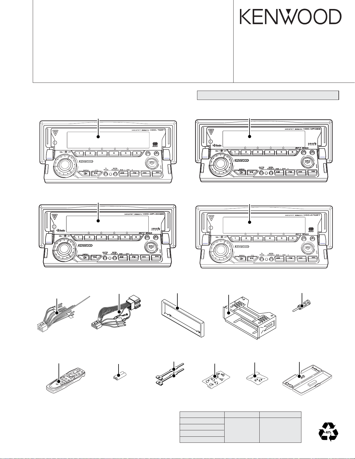
CD mechanism extension cord (24PIN) : W05-0935-00
Panel assy
KDC-8026 (A64-3231-01)
Panel assy
KDC-MPV8025 (A64-3228-01)
Panel assy
KDC-MP825 (A64-3229-01)
Panel assy
KDC-W7027 (A64-3223-01)
* DC cord
(E30-6294-05)
(E30-6295-05)
*Remote controller assy
(A70-2040-05) : RC-505
* Depends on model. Refer to the parts list.
* DC cord
(E30-4942-05)
*Size AA Battery
(Not Supplied)
Escutcheon
(B07-3078-01)
Lever
(D10-4674-04) x 2
TDF PANEL INFORMATION
MODEL PARTS NO. PANEL NAME
KDC-8026
KDC-MP825
KDC-MPV8025
KDC-W7027
Mounting hardware assy
(J21-9823-03)
*Screw set
(N99-1723-05)
Y33-1790-61 TDF-M7000
Screw
(N99-1734-05)
* Antenna adaptor
(T90-0552-05)
Plastic cabinet assy
(A02-2731-13)
KDC-8026/MP825
KDC-MPV8025/W7027
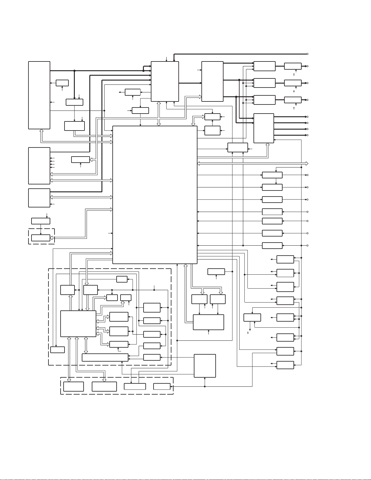
BLOCK DIAGRAM
(X34- )
TUNER
AUDIO OUT
S-METER
CD
CH
BU5V
Q501
EEP5V
IC1
EEPROM
TDF UNIT
(X16-208)
DISPLAY
UNIT
(X16-254)
(X16-255)
SWITCH UNIT
(X16-256)
Q303,304
AM+B
8V
BU5V
8V
SERVO
CD4.7V
BACK UP
IC9
REMO
8V 8V
BUFFER
IC14
RDS
DECODER
EEPROM
SW5V
IC7
LEVEL
SHIFT
IC11
u-COM
ROT ARY
ENCODER
SW5V
LEVEL
SHIFT
IC8
BU5V
IC2
IC4
IC10
FL
KEY
KEY MATRIX
BPF
IC1
MASK
ROM
FLASH
ROM
BPF
SW5V
2.5V
LEDLED
AGC
AGC
8V
BUFFER
SYSTEM
MICROPROCESSOR
ILL+
RESET SW
PANEL5
Q6,10
PANEL
SW5V
IC6
3.3V
Q5
SW3.3V
Q4
FL3.3V
Q2,3
FL+B
IC2
FM
AM
CD
CH
QUAL
E-VOL
MPX
KEY ILL
9V
9V
9V
AUX IN
PRE OUT
(SUB WOOFER)
PRE OUT
(REAR)
PRE OUT
(FRONT)
SP OUT (FL)
SP OUT (FR)
SP OUT (RL)
SP OUT (RR)
WIRED REMO/
OPEL DISP I/F
EXT.AMP.CON
TEL MUTE
ACC
BACK UP
8V
&
8V
IC15
MOTOR
FL+B
FAC
IC5
SYSTEM
E'S+
IC20
FOCUS
SW
IC8
SERVO
PANEL
MECHA
SW5V
DC/DC
WOW
RESET
IC16
MOTOR
DRDR
IC6
BU5V
IC9
8V
8V
MUTE
DRIVER
Q207,208
PRE MUTE
Q203,204
PRE MUTE
Q205,206
PRE MUTE
IC4
POWER
IC
BU5V
IC18
Q23,24
ANT-CON ANT CON
Q25
EXT AMP
Q26
DIMMER DIMMER
TEL MUTE
Q29
ACC DET
Q27
B.U DET
BU5V
SW5V
PANEL5V
SW14V
DC/DC A8V
9V
SERVO
CD4.7V
IC13
IC12
IC11
P-CON P CON
Q1,2
BU5V
Q3,601
SW 5V
Q502,503
PANEL
5V
Q4,5
SW 14V
Q6-8
A8V
Q9,602
SERVO
Q11-14
FL+B
IC19
SW REG
OP AMP
OP AMP
OP AMP
2
KDC-8026/MP825
KDC-MPV8025/W7027
COMPONENTS DESCRIPTION
● SUB CIRCUIT UNIT (X16-2080-10)
Ref No. Application / Functions Operation / Condition / Compatibility
IC1 E2PROM E2PROM for security
● DISPLAY UNIT (X16-2540-10)
Ref No. Application / Functions Operation / Condition / Compatibility
IC1 Driver LCD driver (Include KEY input function)
IC2 Driver LCD driver
IC3 Remote control IC For Remote control sensor
Q1 SW Key scan start SW “ON” when Q1 base level goes L
Q2 Red LED SW Red LED is turned on when Q2 base level goes H
Q5 VLCD AVR Reference voltage
Q6 SW Power supply control SW “ON” when base level goes L
Q11 Dimmer control LCD back light control “OFF” when Q11 base level goes L
D26 VLCD AVR Reference voltage
● DISPLAY UNIT (X16-2550-10)
Ref No. Application / Functions Operation / Condition / Compatibility
IC1 Driver LCD driver (Include KEY input function)
IC2 Driver LCD driver
IC3 Remote control IC For Remote control sensor
IC4 D/A converter For Variable illumination control
Q1 SW Key scan start SW ON when Q1 base level goes L
Q2 Red LED SW Red LED is turned on when Q2 base level goes H
Q5,D26 VLCD AVR Reference voltage
Q6 SW Power supply control SW ON when base level goes L
Q11-16 Illumination control Variable illumination control transistor
Q62-64 Illumination control Variable illumination control transistor
● SWITCH UNIT (X16-2560-11)
Ref No. Application / Functions Operation / Condition / Compatibility
Q1 DSI LED SW DSI LED blinks when Q1 base level goes H/L
Q2 KEY Illumination SW (Green) KEY Illumination SW “ON” when the Q2 base level goes H
Q3 KEY Illumination SW (Red) KEY Illumination SW “ON” when the Q3 base level goes H
Q4 KEY Illumination SW (Blue) KEY Illumination SW “ON” when the Q4 base level goes H
● CD PLAYER UNIT (X32-5540-00)
Ref No. Application / Functions Operation / Condition / Compatibility
IC1 Mechanism control microprocessor -
IC2 DSP CD signal processor, RF amp, Servo control
IC3 Decoder IC MP3/WMA decoder
IC4 BTL driver Focus, Tracking coil, Feed and Spindle motor driver IC
IC5 AVR SW3.3V AVR
IC6 AVR BU3.3V AVR
3
KDC-8026/MP825
KDC-MPV8025/W7027
COMPONENTS DESCRIPTION
Ref No. Application / Functions Operation / Condition / Compatibility
IC7 AVR BU2.5V AVR
IC8 Selector IC Serial audio data selector
IC9 AVR 3.3V AVR (IC2 DAC part)
Q1,4 Level shift FET Level shift (3.3V - 5.0V)
Q3,5 Level shift TR Level shift (3.3V - 5.0V)
Q6 Level shift TR Level shift (3.3V - 5.0V)
Q7 Level shift TR Level shift (3.3V - 5.0V)
Q8 APC Auto power control
Q9,10 Switching TR Sub beam delay control switch
● ELECTRIC UNIT (X34-3040-10/11/21, X34-3042-71)
Ref No. Application / Functions Operation / Condition / Compatibility
IC1 System control IC System control microprocessor
IC2 E-VOL & tuner IC E-VOL. FM/AM tuner & stereo decoder
IC3 Power supply IC For A8V AVR
IC4 Audio power IC Audio power amplifier
IC5 Power supply IC Switching regulator IC for CD5V
IC7 Reset IC When BU5V line voltage is less than 3.5V, this IC output line is “L”
IC8 Muting logic IC Control for MUTE, P-ANT & RESET muting
IC12 RDS decoder Decode for RDS signal
IC13,14 Motor driver Control for Panel mechanism motor
Q1,2 BU 5V AVR While BU is applied when BU5V regulator output is +5V
Q3 SW5V AVR When Q3base level goes L, SW5V regulator output is +5V
Q4,5 SW14V AVR When Q5 base level goes H, SW14V regulator output is +14V
Q6-8 Audio 8V AVR When Q6 base level goes H, A8V regulator output is +8.4V
Q9,34 Servo +B AVR When Q34 base level goes H, S+B regulator output is +7.4V
Q11~14 Illumination +B AVR When Q11 base level goes H, AVR output is +10.5V
Q23,24 P-ANT SW When Q23 base level goes H, P-ANT SW output is +14V
Q25,26 P-CON SW When Q26 base level goes H, P-CPN SW output is +14V
Q27,28 P-CON protection Protect Q27 by turning on when P-CON output is grounded
Q29 Buffer EX amp control buffer
Q30 Small lamp det. SW When Q30 base level goes H, Q30 turned ON
Q32 BU detector When Q32 base level goes H, Q32 turned ON
Q33 ACC detector When Q33 base level goes H, Q33 turned ON
Q51,52 Muting driver When base level goes L, muting driver is turned ON
Q55,56,59,60
Q63 E2P 5V SW When Q63 base level goes L, E2P 5V is out for E2P ROM
Q102,103 AM +B SW When Q102 base level goes H, AM +B is out to tuner unit
Q104 Buffer Composite signal buffer for RDS
Pre-out muting SW When base level goes H, Pre-output is muted
4
KDC-8026/MP825
KDC-MPV8025/W7027
MICROCOMPUTER’S TERMINAL DESCRIPTION
● SYSTEM MICROPROCESSOR : UPD703030GC042 (X34-304 : IC1)
Pin No. Pin Name I/O Description / Processing Operation
1 PLL DATA I/O Data input/output terminal for Tuner front-end
2 AM+B I/O AM+B (AM operation : H)
3 (FM+B) O FM+B (FM operation : H, Last FM : H with RDS,RBDS model)
4PAN E2P DATA I/O Variable illumination D/A converter, E2PROM DATA terminal
5PAN E2P CLK I/O Variable illumination D/A converter, E2PROM CLK terminal
6 EVDD - VDD 5V
7 EVSS - GND
8 AFS O Time constant switching for noise detection (FM seek, AF search, AUTO 0 : L, Receiving : H)
9 BEEP O BEEP audio output terminal
10 REMO I Remote control input terminal
11 P MUTE O Audio power IC muting control terminal (POWER OFF, ALL OFF, TEL MUTE : L)
12 SVR O Audio power IC SVR discharge circuit control terminal
13 IC2 SDA I/O CD mechanism, IC2, IC5, ROM correction DATA line
14 IC2 CLK I/O CD mechanism, IC2, IC5, ROM correction CLOCK line
15 P STBY O Audio power IC Stand-by terminal (POWER IC ON, ALL OFF : H, POWER IC OFF : L)
16 P CON I/O Power control terminal (POWER ON : H, POWER OFF, ALL OFF : Hi-Z)
17 DIMMER CONT O Dimmer control terminal (W-LED only : Pulse control F=1KHz, Normal : H)
18 TEST - NC (GND)
19 TYPE2 I Destination select terminal
20 MUTE O MUTE output terminal (ON : OPEN, OFF : L)
21 PRE MUTER O PREOUT (Rch) muting control terminal
22 PRE MUTEL O PREOUT (Lch) muting control terminal
23 BU DET I
24 ACC DET I ACC detection terminal (With ACC : L, Without ACC : H)
25 SW5V I/O SW5V control terminal (OFF : H, ON : L)
26 EXT AMP CONT O External amplifier control terminal
27 DIMMER I Small lamp detection terminal (ON : L, OFF : H)
28 ANT CONT I/O Antenna control/ Destination select terminal (TUNER ON : H)
29 P ON I/O SW14V, SW5V control terminal (POWER ON : H, POWER OFF : Hi-Z)
30 ILL ON I/O FL, illumination control terminal (ON : H, OFF : Hi-Z)
31 RESET I Reset input terminal
32,33 XT1/XT2 - Sub clock (32.768kHz)
34 REGC - Connect to 1µF capacitor
35,36 X2/X1 - Main clock (20MHz)
37 VSS - GND
38 VDD - AVR 5V
39 CLKOUT - NC
40 LX REQ M O Communication request to external slave unit (Request : L)
41 LX MUTE I Mute request from external slave unit (MUTE : H)
Momentary power dropped detection terminal (No Backup, Momentary power dropped : H, Backup : L)
Fig.
5
KDC-8026/MP825
KDC-MPV8025/W7027
MICROCOMPUTER’S TERMINAL DESCRIPTION
Pin No. Pin Name I/O Description / Processing Operation
42 LX CON O External slave unit (ON : H, OFF : L)
43 LX RST O Reset output to external slave unit (Normal : L, After system reset : H 400ms or more and then L)
44 CD MECHA+B O CD4.7V output terminal (CD : H, Except CD source : L)
45,46 TYPE0/TYPE1 I Destination select terminal
47,48
49 NC - NC
50 E2P5V I/O E2PROM, D/A converter power supply control terminal (ON : L, OFF : Hi-Z)
51 DSI I/O DSI control (ON : L, OFF : Hi-Z)
52 L CE O CE output to LCD driver IC
53 L INH O INN output to LCD driver IC (Normal : H, Reset, Momentary power dropped : L)
54 VOL A I Volume input terminal
55 DVDD - AVR 5V
56 DVSS - GND
57 VOL B I Volume input terminal
58 M RST O Reset output to CD mechanism (Normal : H, Reset : L)
59 M STOP O Stop request to CD mechanism (STOP : L, CD : H)
60 CD SW3 I CD DOWN SW detection terminal (CD disc chucking : H)
61 LO/EJ I/O CD mechanism loading/ eject selector (STOP, Brake : Hi-Z, LOADING : L, EJECT : H)
62 MOSW O CD mechanism motor driver SW (LOADING, EJECT, Brake : H)
63 FPM MOTOR B O FPM mechanism (Slider) control terminal 1
64 FPM MOTOR F O FPM mechanism (Slider) control terminal 1
65 FPM MOTOR O O FPM mechanism (Angle) control terminal 1
66 FPM MOTOR C O FPM mechanism (Angle) control terminal 1
67 O DATA I/O External display DATA terminal 1
68 O CLK I/O External display CLK terminal
69 O CE I/O External display chip enable terminal
70 M MUTER I Mute request from CD mechanism (Rch ON : L)
71 AVDD - AVR 5V
72 AVSS - GND
73 AVREF I Connect to P-ON (29PIN)
74 M MUTEL I Mute request from CD mechanism (Lch ON : L)
75 PAN DET I PANEL, E2PROM detection terminal (With panel : L, Without : H)
76 PHONE I PHONE detection terminal (TEL MUTE : 1V or less, NAVI MUTE : 2.5V or more)
77 FPM SW4 I
78 FPM SW1 I FPM mechanism position detect terminal 1
79 FPM SW2 I FPM mechanism position detect terminal 1
80 FPM SW3 I FPM mechanism position detect terminal 1
81 FPM PHOUT I FPM mechanism position detect terminal (2.2V or more : H) 1
82 S METER I S meter detection terminal
IC2 TYPE0/TYPE1
I IC2 destination select terminal
FPM mechanism position detect/ CD Mechanism detection terminal
(3.75V or more : No mechanism, 1.25V or more : H, Less than 1.25V : L)
1
6
MICROCOMPUTER’S TERMINAL DESCRIPTION
Pin No. Pin Name I/O Description / Processing Operation
83 NOISE I FM noise detection terminal
84 IFC OUT I Front end IFC OUT input terminal (Receiving station : 2.5V or more)
85 POWER DET I Audio power IC DC offset detection
86 CD SW4 I 8cmDISC detection terminal (8cmDISC : L)
87 R CLK I RDS decoder clock input terminal
88 LX REQ S I Receive request from external slave unit (Request : L)
89 SC REQ I Communication request from panel microprocessor
90 CD SW1 I LOADING SW detection terminal (LOADING start, POWER OFF : L)
91 CD SW2 I 12cmDISC detection terminal (12cmDISC, POWER OFF : L)
92 R QUAL I RDS decoder QUAL input terminal
93 R DATA I RDS decoder DATA input terminal
94 LX DATA S I Data input from external slave unit
95 LX DATA M O Data output to external slave unit
96 LX CLK I/O Clock input/ output with external slave unit
97 L DATAL I Data input from LCD driver
98 L DATAS O Data output to LCD driver
99 L CLK O CLK output to LCD driver
100 PLL CLK I/O Clock input/ output to Tuner front-end
KDC-8026/MP825
KDC-MPV8025/W7027
Fig.1 FPM motor control
SLIDE FPM mechanism
FPM MOTOR B FPM MOTOR F operation
LLStandby
HLBackward operation
LHForward operation
HHBrake
FPM MOTOR O FPM MOTOR C operation
ANGLE FPM mechanism
LLStandby
HLAngle open direction
LHAngle close direction
HHBrake
● MECHANISM CONTROL MICROPROCESSOR : 91CW12AFG-4VF6 (X32-554 : IC1)
Pin No. Pin Name I/O Description / Processing Operation
1 VREFL I Reference voltage input terminal
2AVSS - GND for ADC
3AVCC - Power supply for ADC (BU3.3V)
4NCONC (OPEN)
5 20RST O Reset control output terminal (for decoder) L : RESET, H : NORMAL
6 20ACK I Acknowledge signal input terminal (for decoder)
7 20STBY O Standby control (for decoder) H : STAND BY, L : NORMAL
8,9 NC O NC (OPEN)
10 20INT I Interrupt signal input terminal (for decoder)
11 FOGUP I Interrupt for focus gain up control signal H : Focus gain UP, L : NORMAL
7
KDC-8026/MP825
KDC-MPV8025/W7027
MICROCOMPUTER’S TERMINAL DESCRIPTION
Pin No. Pin Name I/O Description / Processing Operation
12 LZM I 0bit muting detect (Lch) L : MUTE OFF, H : MUTE ON
13 RZM I 0bit muting detect (Rch) L : MUTE OFF, H : MUTE ON
14,15 NC O NC
16 20CS O Chip select signal output terminal (for decoder)
17 20LP O Latch pules signal output terminal (for decoder)
18 20TXD0 I/O Serial data signal output terminal (for decoder)
19 20RXD0 I Serial data signal input terminal (for decoder)
20 20SCLK0 O Serial data clock output terminal (for decoder)
21 DSPTXD1 O Serial data signal output terminal (for DSP)
22 DSPRXD1 I Serial data signal input terminal (for DSP)
23 DSPSCLK1 O Serial data clock output terminal (for DSP)
24 AM0 I Select for ROM mode H : NORMAL, L : External ROM mode
25 DVCC - BU3.3V
26 X2 O Oscillator (16MHz)
27 DVSS - GND
28 X1 I Oscillator (16MHz)
29 AM1 I BU3.3V
30 RESET I Reset terminal L : RESET, H : NORMAL
31,32 NC O NC
33,34 EMU0,1 O NC
35 DSPSTB O Data strobe signal output terminal
36 DSPA0 O Command, parameter select signal H : Parameter, L : Command
37 DSPRST O Reset control output terminal (for DSP)
38 DSPINT I Interrupt signal input terminal (for DSP) H : Interrupt
39 /DAC RESET O Reset signal output terminal (for DSP) L : RESET, H : NORMAL
40 SEARCH O Search condition output terminal H : Search, L : NORMAL
41 LOE/LIM_SW I SLT SW detect input terminal H : Inside
42~45 NC O NC (OPEN)
46 PONE5 O +5V AVR control terminal (for VIDEO) H : Power ON
47 PONE2.5 O +2.5V AVR control terminal (for VIDEO) H : Power ON
48,49 NC O NC (OPEN)
50 FLAGIN I C2 error detect terminal L : Correction OK, H : Correction NG
51~60 NC O NC (OPEN)
61 /DAC PD O Reset control output terminal (for DAC) L : RESET, H : NORMAL
62 DVSS - GND
63 NMI I Request for non maskable interrupt signal input terminal
64 DVCC - +VCC
65 DAC MUTE O Muting control output terminal (for DAC) H : MUTE, L : MUTE OFF
66 DAC PON O Audio power supply (for DXM-6550) H : POWER ON
67 PONA5 O +5V Audio power supply (for DXM-6550) H : POWER ON
8
KDC-8026/MP825
KDC-MPV8025/W7027
MICROCOMPUTER’S TERMINAL DESCRIPTION
Pin No. Pin Name I/O Description / Processing Operation
68 ESRST O Reset signal output terminal (for ES3890) L : RESET, H : NORMAL
69 VMUTE O Video mute control terminal H : MUTE ON, L : MUTE OFF
70 NC O NC (OPEN)
71 SELINT O Video/Audio select output terminal H : NORMAL, L : Interrupt
72 ASEL0 O Audio signal output select control terminal 1 00 : STEREO, 01 : Lch
73 ASEL1 O Audio signal output select control terminal 1 10 : Rch, 11 : Not function
74 NT/PAL O NTSC/PAL select terminal L : NTSC, H : PAL
75 DATASEL O 20F/ES3890 output select H : 20F, L : ES3890
76,77 NC O NC (OPEN)
78 NC(BOOT) I Flash memory writing terminal L : Writing, H : NORMAL
79,80 NC O NC (OPEN)
81 POND3.3 O D3.3V power ON control terminal H : POWER ON
82 MUTEL O Audio muting control terminal (Lch)
83 MUTER O Audio muting control terminal (Rch)
84 SDA I/O I2C data (for system microprocessor)
85 SCL I/O I2C clock (for system microprocessor)
86 MSTOP I Interrupt signal for stand-by mode L : STOP, H : STOP cancellation
87 NC O NC
88 DMUTE O Driver muting control L : MUTE ON, H : MUTE OFF
89 DVCC - +VCC
90 NC O NC (OPEN)
91 DVSS - GND
92,93 NC I NC
94 MSEL I Memory capacity select input terminal H : Capacity Down, L : Capacity UP
95 VCDSEL I NC
96 ASEL I Audio signal output polarity selector H : Reversal output, L : Noninversion output
97 CHSEL I Changer detect input terminal H : Changer, L : Normal
98 SEL0 I Destination input terminal DXM6540 (SEL0 : Lo, SEL1 : Lo)
99 SEL1 I Destination input terminal DXM6540 (SEL0 : Lo, SEL1 : Lo)
100 VREFH I ADC reference power supply (BU3.3V)
9

KDC-8026/MP825
KDC-MPV8025/W7027
TEST MODE
● How to enter the test mode
While pressing and holding the Preset 1 and Preset 3 keys,
reset the unit.
● How to exit from the test mode
While holding the Preset 6 key, reset the unit.
Note : Turning ACC off, po wer off, momentary power down
or panel detaching does not terminate the test mode.
● Initial status in the test mode
• Sources : ALL OFF
• Display : All segments are lit.
• Volume : -10dB (displayed as “30”)
• Loudness : OFF
• CRSC : OFF regardless of the presence of switching function.
• SYSTEM Q : Flat
• WOW : All OFF
• BEEP : When pressing any keys, the buzzer generates a
beep at any time.
• AUX : ON
• MENU SYSTEM Q : OFF
• Variable model : Default is white
• Multifunction : Source dependency (Preset, SCAN, etc.)
● Special display in Tuner mode
When any of the following messages is displayed in Tuner
mode, the F/E may be abnormal.
• “TNE2P NG” : The EEPROM is set to the default (unstable
values) because the F/E was shipped without passing
through the adjustment process, etc.
• “TNCON NG” : Comm unication with the F/E is not possible.
● Forced switching of K3I
Each press of the Preset 6 key in Tuner mode should switch
K3I from AUTO→Forced Wide→Forced Middle→Forced
Narrow→AUTO.
The initial status is AUTO and the display shows these
modes as follows.
• AUTO : FMA
• Forced Wide : FMW
• Forced Middle : FMM
• Forced Narrow : FMN
● Test mode specifications of the CD receiver
•Forced ejection is inhibited in the reset start operation. When
the unit is reset while a CD is loaded in it, resetting does
not recognize the CD.
• Each press of the Track Up key jumps to the f ollowing track
numbers :
No. 9→No. 15→No. 10→No. 11→No. 12→No. 13→No. 22
→No. 14→No. 9 (The cycle restarts from here.)
• Each press of the Track Down key jumps to the previous
track number to the track being played.
•When the number of total trucks of the MP3 disc or the
WMA disc is less than 9, 1st truck is played.
• When the disc media is CD, A short press of the Preset 1
key jumps to the track number 28.
• When the model is equipped the CD mechanism assembly
adapted for MP3 or MP3/WMA disc, the mechanism name
and version number are displayed during the FL model is
lower stand and Display mode of LCD model is DNPS.
● Audio-related specifications
• Pressing the ✽ ke y on the remote initiates the audio adjustment mode.
• BL/F key on the Fader initials.
• Continuous holding of a remote control key is inhibited, and
workings are short press of any keys.
• Bass, Middle and Treble are adjusted in 3 steps of -8 / 0 /+8
with the Track Up/Down keys (Default value at 0).
• Balance is adjusted in 3 steps of L15 / 0 / R15 with the
Track Up/Down keys (Default value at 0).
•Fader is adjusted in 3 steps of R15 / 0 / F15 with the Track
Up/Down keys (Default value at 0).
• HPF is adjusted in 2 steps of OFF / 170Hz (or 200Hz) with
the Track Up/Down keys (Default value at OFF).
• LPF is adjusted in 2 steps of OFF / 120Hz with the Track
Up/Down keys (Default value at OFF).
• Bass f, Bass Q, Bass EXT, Middle f, Middle Q and Treble f
are not dealt with by the audio adjust.
• The WOW key passes during the audio adjustment as following steps (WOW model only).
Ordered TruBass FOCUS SRS Display
1 OFF OFF OFF SRS WOW OFF
2ONOFF OFF SRS TruBass ON
3 OFF LOW OFF FOCUS LOW
4 OFF HIGH OFF FOCUS HIGH
5 OFF OFF ON SRS ON
6ONHIGH ON SRS WOW HIGH
10
TEST MODE
KDC-8026/MP825
KDC-MPV8025/W7027
● Menu-related specifications
• A short press of the Q key initiates the menu mode.
• Pressing the DNPP key on the remote initiates the Menu
mode.
• Continuous holding of a remote control key is inhibited, and
workings are short press of any keys.
• Contrast is adjusted in 3 steps of 0 / 5 / 10 with the Track
Up/Down keys (Default value at 5).
● Backup current measurement
When the unit is reset while ACC is OFF (i.e. by turning
Backup ON), the MUTE terminal goes OFF in 2 seconds in
place of 15 second. (The CD mechanism is not activated at
this time.)
● Special display when the display is all on
Pressing the Preset keys while the power is ALL OFF displays the following information.
[PRESET 1]
[PRESET 2]
[PRESET 3]
[PRESET 4]
[PRESET 5]
[PRESET 6]
FM key Display ROM collection version.
Version display (8 digits, Month/Day/Hour/Minute)
(Display) SYS xxxxxxxx :
PAN xxxxxxxx : FL model only
MEM
xxxxxxxx :
Serial number display (8 digits)
(Display) SNo xxxxxxxx
Short press : View power ON time. (The All OFF
period is not counted.)
2 seconds long press/hold : Clear power ON time
at the power ON time displaying.
(Display) PonTim xxxxx Max. 60000 (hours)
Short press : Display CD operation time.
2 seconds long press/hold : Clear CD operation
time at the CD operation time displaying.
(Display) CDTim xxxxx Max. 60000 (hours)
Short press : Display CD ejection count.
2 seconds long press/hold : Clear CD ejection
count at the CD ejection count displaying.
(Display) EjeCnt xxxxx Max. 60000 (times)
Short press : Display Panel open/close count.
2 seconds long press/hold : Clear Panel open/close
count at the Panel open/close count.
(Display) PnCnt xxxxxx Max. 600000 (times)
(Display) ROM R xxx Invalid : “R – – –”
4 contrasts FL model only
AM key Display panel E2PROM condition.
(Display) P–ROM OK (Registered code)
P–ROM NG (Code is write in error)
P–ROM WAIT (Unregistered code)
P-ROM NON
(Panel security nonfunctional)
● Panel mechanism
• Auto-panel close inhibition when set-in the CD.
• The panel operation inhibition at power ON/OFF and ACC
ON/OFF.
• The panel position changing Eject→Last with a short press
of the PLAY/PAUSE keys.
● Other specifications
• No displays such as “CODE OFF/ON” during Power-ON.
• The LINE MUTE inhibition time is one second from 10 seconds when start-up the test mode.
• Do not write the security code with the security jig on the
test mode.
• Do not write the serial with the serial writing jig on the test
mode.
• OEM display output is not stop if OEM display not connection on the test mode.
● Switching the frequency span (K/M type)
While holding the Preset 1 key and Preset 5 key, reset the
unit.
● Demonstration mode
1. How to enter to the Demonstration mode
1. Hold down the [Q] key and [TI (AME)] k ey button when the
power is on and press the Reset button.
2. This will enter to the Demonstration mode.
2. How to chancel the Demonstration mode
1. Hold-down the Preset [5] key button when the power is on
and press the Reset button.
2. This will cancel the Demonstration mode.
11

KDC-8026/MP825
KDC-MPV8025/W7027
TEST MODE
● Security information
1. Forced Power ON mode (All models)
Even when the security (Cord) is approved, resetting the
unit while holding the Q and Preset 4 keys makes it possible to turn the power ON for 30 minutes.
After 30 minutes have elapsed, it is not possib le to return to
the previous condition unless the unit is reset again. (Security code is doing not clear at this mode. Put the power on
fill-in.)
When panel security was set up for the unit when it is can
not power on.
In this case, you can use new ROM for the TDF panel that
the unit can be power on for test mode.
Note : Don’t enter the panel security set up for new ROM
panel. User can not power on the unit.
2. Method of registration of the security code after
EEPROM (F/E) replacement (Code security model)
1. Enter the test mode. (See How to enter the test mode)
2. Press the MENU key to enter the Menu mode.
3. When the message “Security” is displa yed, press and hold
the Track Up/Down key for 1 second to enter the security
registration mode.
4. Enter the code using the FM/AM/T r ack Up/Track Down keys.
FM key : Number up
AM key : Number down
Track Up key : Cursor right shift
Track Down key : Cursor left shift
5. Hold down the Track Up key for at least 3 seconds and the
message, “RE-ENTER” appears, so once again enter the
code according to Step 4 above.
6. Press and hold the Track Up key for 3 seconds until “APPROVED” is displayed.
7. Exit from the test mode. (See 2. How to exit from the test
mode)
Note 1 : All Clear is not applicable to the security code of
this model.
Note 2 : When the F/E changed, need re-inscription because the panel security is clear.
3. How to inscription the panel security code
1. Enter the test mode.
2. Pressing the AM key on all lighting, check the “P-ROM W AIT”
display.
3. The NEXT key is long press 2 seconds, writing the code.
4. Display is “P-ROM OK”.
5. Exit from the test mode.
Note : E2PROM connection is NG when displa y is “P-R OM
NG”, so detach the panel and rewrite after the display is
“PROM WAIT”. This code can not clear.
4. Simple way to c lear the security code (K type only)
1. During code request mode, press the Track UP key for at
least 3 seconds while holding down the A UTO key. (– – – –
will disappear)
2. Enter, “KCAR” with the remote controller as described below.
• Press the remote controller 5 key twice, and press the Track
Up key. (Enters a “K” )
• Press the remote controller 2 key three times, and press
the Track Up key. (Enters a “C” )
• Press the remote controller 2 key once, and press the Track
Up key. (Enters an “A” )
• Press the remote controller 7 key twice, and press the Track
Up key. (Enters an “R” )
3. Security function is canceled and unit sets to All-Off mode.
4. Code request mode appears if a mistake was made in entering the numbers.
12
EDCBA
KDC-8026/MP825
KDC-MPV8025/W7027
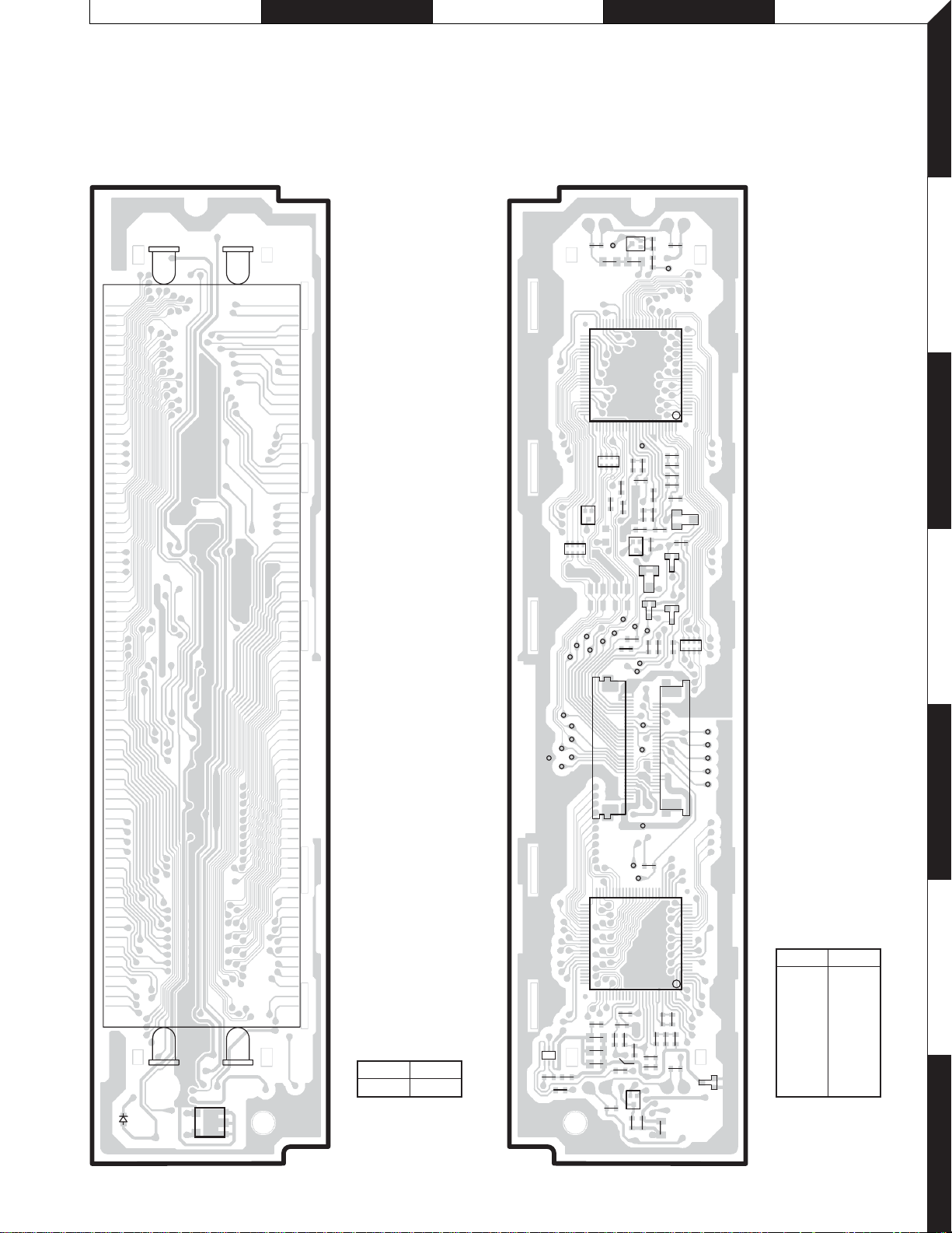
PC BOARD
(COMPONENT SIDE VIEW) (FOIL SIDE VIEW)
DISPLAY UNIT
X16-2540-10 (J74-1588-02)
D16
72
DISPLAY UNIT
X16-2540-10 (J74-1588-02)
R54
Q11
EB
R14
R7
R52
IC1
R11
R67
R68
1
32
C6
C4
EB
D1
E2P5V
R8
DSI
C26
R53
VLCD1
C2
R5
R4
R3
R12
D3
E2PCLK
R13
28
RST
1
ILLGND
DIMMER
26
100
R6
R23
KS4
KS3
KS2
KS1
ESDGND
VOLA
CP4
KI1
KI2
VOLB
//
C27
ILLGND
50
51 75
76
Q1
EB
KI3
KI4
CN2
R51
CP5
R26
C3
Q5
GREEN
KI5
RED
E2PDATA
PANDET
R1
C1
R2
C2
25
1
R24
D5
D4
CN1
D26
CP1
CLK
DATAS
DATAL
INH
CE
1
2
3
4
5
144 73
D11
D19
DGND
REMO
50
51 75
76
1
X16-2540-10
Ref. No. Address
D18 D17
IC3
23
1
IC3 7A
Q2
R19
CCB
EEB
R16
R17
R20
C19
C18
C17
R18
C28
C16
C12
R36
IC2
R35
EB
ILL+B
R9
VLCD1
C14
PAN5V
C13
Q6
R15
R31
R10
R33
R34
C7
C12
C29
26
100
C11
R32
25 1
X16-2540-10
Ref. No. Address
IC1 3D
6
IC2 6D
Q1 3C
Q2 6C
Q5 4D
Q6 7D
D2
Q11 2D
Refer to the schematic
diagram for the values of
7
resistors and capacitors.
13
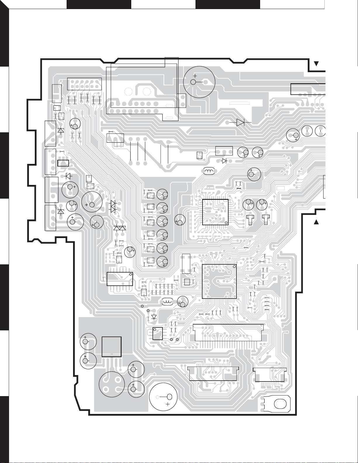
F G H I J
C
KDC-8026/MP825
KDC-MPV8025/W7027
1
PC BOARD (COMPONENT SIDE VIEW)
ELECTRIC UNIT X34-304x-xx (J74-1474-22)
CN1
CN2
2
Q12
Q13
3
Q8
Q1
Q9
4
5
12
11
2
1
R43
BE
BE
R112
Q11
D6
BEBEBEBE
C8
R105
OGI
IC3
D3
C104
D4
C109
R44
C102
R32
C7
R31
C6
Q4
BE
C108
C110
2
1
R55
BE
R56
Q5
C213
9
8
R127
Q24
BE
W1
D14
D15
D16
C105
C132
R140
R139
R141
R138
EB
Q32
IC8
IC5
R125
D17
17
148
C131
R126
5V
Q60
Q59
Q55
Q56
Q58
Q57
R102
R103
EB
Q3
RST
R143
R48R47R23R35
R24R36
R46
EB
EB
R21
EB
EB
R34
EB
EB
R33
R207
1
4
16
1
J1
R45
R22
R265
IC15
L1
R283
R282
R128
R206
R204
D20
R205
R203
L4
8
5
DATA
R129
R209
R211
R214
C50
C49
C41
C42
C46
C45
R208
R210
C207
X2
R202
C208
CLK
C252
C200
R215
C100
2
1
D1
C32
C256
Q25
BE
Q26
23
BE
L6
D13
IC2
33
TEST
25
26
R201
IC1
X1
R200
50
R217
R216
R218
R219
R220
1222
4434
CN4
C128
C126
C250
C254
C253
R300
11
C1 C2
D26
D25
1
1
100
76
7551
R228
R268
R262
R230
R260
L5
R275
124
R257
R259
R250
R252
R253
R256
R251
R234
R235
R236
R237
I
C34
6
15
C111
L2
C112
C113
C700
128
CN5
P1
CN6
115
7
14
 Loading...