Kenwood KD-CMP-8017 Service Manual
©
2001-3 PRINTED IN JAPAN
B51-7755-00 (N) 3386
CD RECEIVER
KDC-MP6090R/MP7018
KDC-MP8017
SERVICE MANUAL
47W 4
X
KDC-MP8017
DAB
47W 4
X
KDC-MP7018
DAB
47W 4
X
KDC-MP6090R
DAB
PTY
TI
VOL ADJ
K
3i
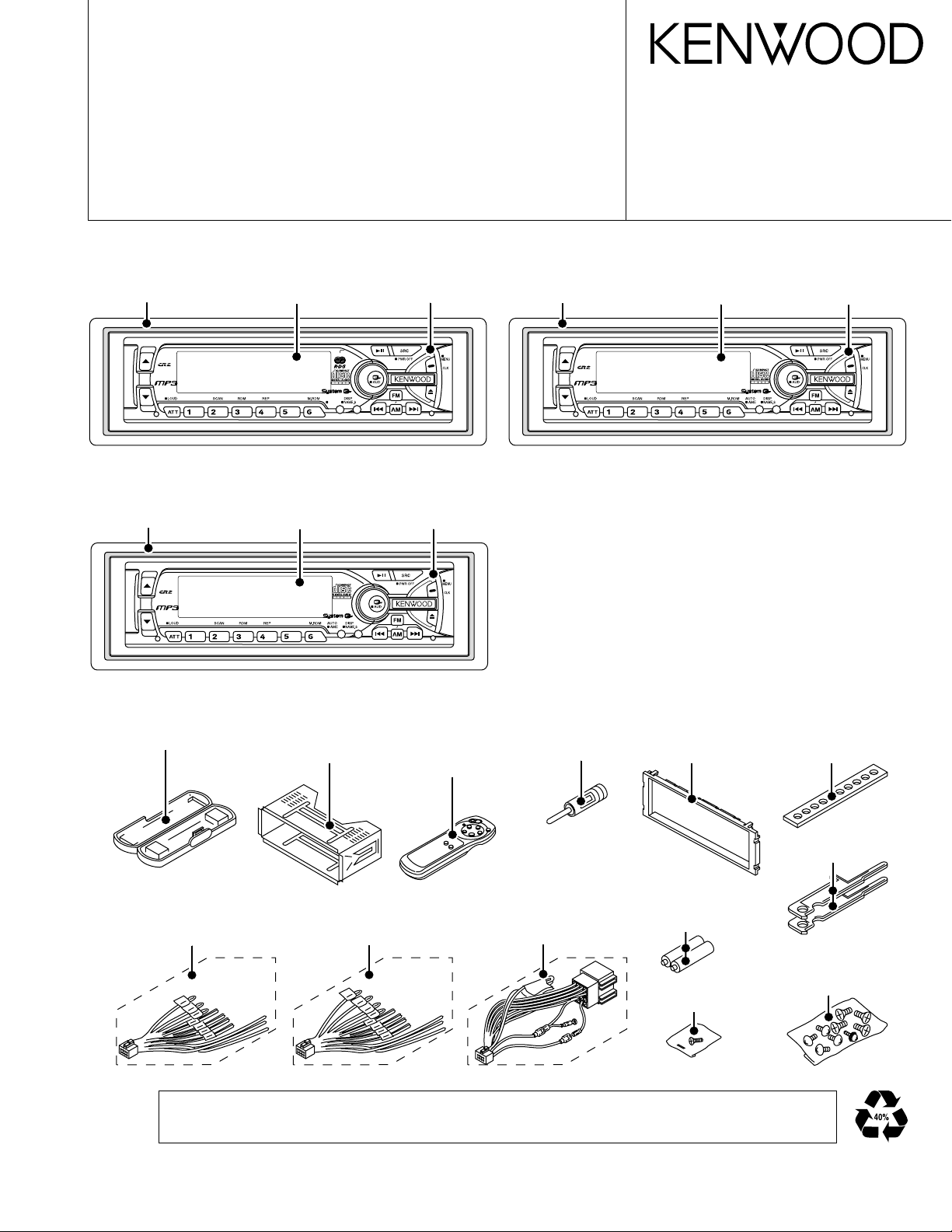
KDC-MP8017
KDC-MP7018
KDC-MP6090R
ESCUTCHEON ASSY
(B07-3007-03)
PANEL ASSY
(A64-2267-02)
PANEL ASSY
(A64-2266-02)
ESCUTCHEON ASSY
(B07-3007-03)
DC CORD
(E30-4940-05)
: KDC-MP8017
DC CORD
(E30-4939-05)
: KDC-MP7018
ANTENNA
ADAPTOR
(T90-0523/0534-05)
: KDC-MP6090R
BATTERY
(SIZE: AAA)
Not supplied as
service parts
SCREW SET
(N99-1704-05)
SCREW SET
(N99-1700-05)
: KDC-MP8017
KDC-MP7018
STAY
(J54-0606-04)
: KDC-MP8017
KDC-MP7018
LEVERx2
(D10-4562-04)
ESCUTCHEON
(B07-3010-02)
: KDC-MP8017
KDC-MP7018
REMOTE
CONTROLLER
ASSY
(A70-0883-05)
: KDC-MP7018
MOUNTING
HARDWARE
ASSY
(J21-9641-13)
PLASTIC
CABINET ASSY
(A02-1497-03)
ESCUTCHEON ASSY
(B07-3007-03)
FRONT GLASS
(B10-4033-01)
FRONT GLASS
(B10-4034-01)
FRONT GLASS
(B10-4035-01)
PANEL ASSY
(A64-2268-02)
DC CORD
(E30-4943-05)
: KDC-MP6090R
The MECHANISM OPERATION DESCRIPTION is the same as model KDC-S3007 and KDC-5050RG.
Please refer to the service manual for model KDC-S3007(B51-7029-00) or KDC-5050RG(B51-7099-00).
KDC-MP6090R/MP7018/MP8017
2
BLOCK DIAGRAM
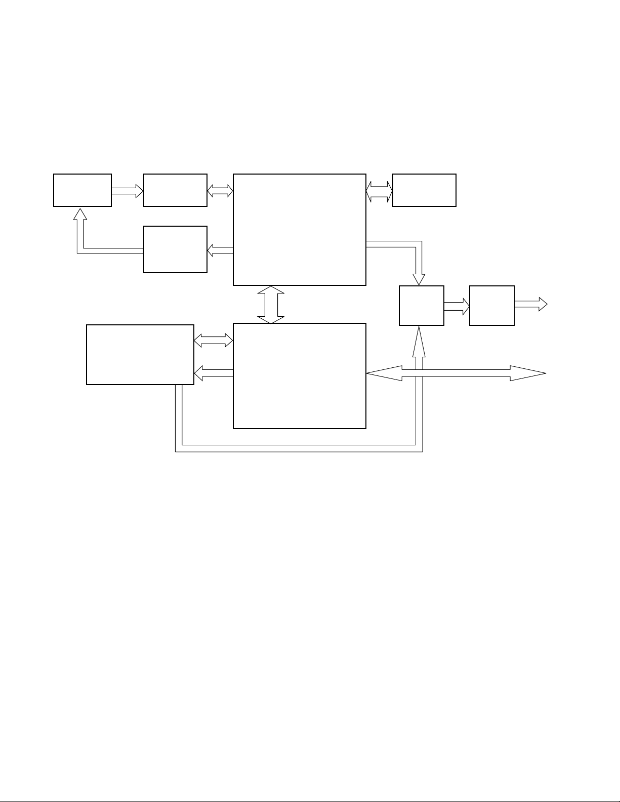
DMX-1760 BLOCK DIAGRAM
ANALOG
OUT
COMMUNICATION TO HOST
IC2 CONTROL
IC3 CONTROL
MP3 BIT CONTROL
MP3 TIME DISPLAY
CD TEXT CONTROL
FILE ANALISIS (ISO9660)
IIS DATA
SERVO CONTROL
EFM DECODE
ROM DECODE
ATAPII/F (NOT USED)
MP3 DECODE
IC2
IC11
DPU1
CD PICK UP
IC10
IC1
IC6
IC3 IC9,12
IC5
RF AMP
(4Mbit)
D-RAM
MUX
LPF
DAC
CD-ROM DECODER
SERVO CONTROLER
MECHA CONTROL COMPUTER
4cH BTL
DRIVE
MPEG 2.5 LAYER III
AUDIO DECODER
IIC
MPEG
KDC-MP6090R/MP7018/MP8017
3
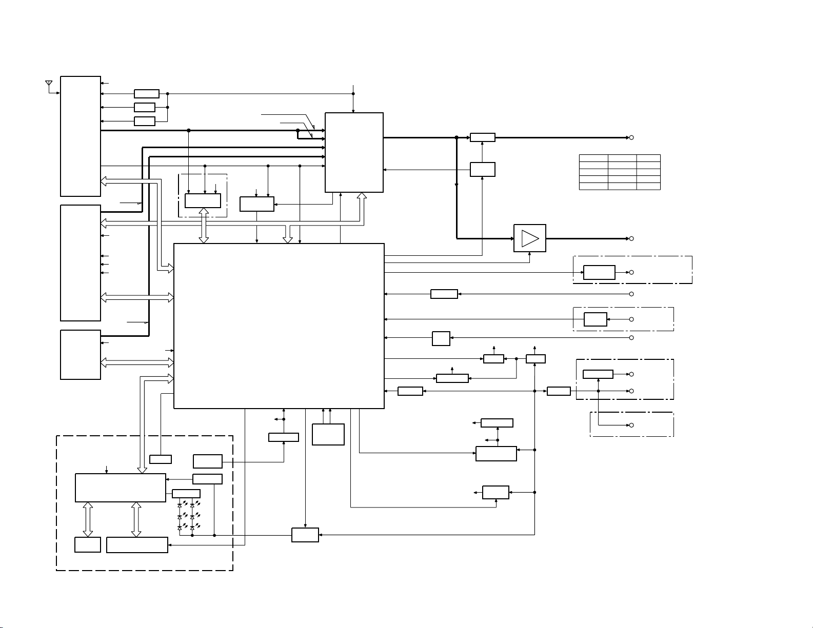
BLOCK DIAGRAM
PLL+B
FM+B
Q45,47
Q46,48
AM+B
DIMMER
MUTE
2WAY
DET.
ACC
BU DET.
A8V
A8V
IC10
Q14-16
Q19-22
IC8
SERVO AVR
IC11
Q17
SERVO+B
SW5V
Q13
Q55,56
Q33
Q11,12
SW5V
BU5V
BU5V
P CON
ANT-CON
Q28,31
Q27,29
Q30,32
MUTE
IC3
Q7
DRIVER
MUTE
Q1,2,5,6
POWER IC
IC4
u-COM
CD
CH
F/E
A1
E-VOL
IC2
PRE OUT
SP-OUT
DIMMER
TEL-MUTE
ACC
ANT-CONT
P-CONT
ANT-CONT
P-CONT
DECODER
RDS
(E)TYPE
IC1
IC7
Q52
EX.AMP CONTROL
ILLUM
+B
BUFFER
NOISE
Q51
PRE OUT OUTPUT VOLTAGE
CONTROL
EX.AMP
Q25
Q26
Q34
(M,E) TYPE
(E) TYPE
(E) TYPE
(K,M) TYPE
NAVI-MUTE
PANEL 5V
PANEL 5V
PANEL
POSITION
DET.
CH
QUAL
SERVO+B
MUTE R
STOP
SW2
LO/EJ
MUTE L
RST
SW3
SW1
SDA
SCL
A8V
BU5V
SW5V
RST
REQ C
CLK
CH-CON
DATA H
REQ H
CD
AM
FM
P MUTE
MUTE
SW5V
PANEL5V
ILL+B
SRT-SW1
SRT-SW2
P ON
SERVO+B
RDCK
RDDA
QUAL
SDA
SCL
AFS
AFS
A8V
PLL DATA
PLL CLK
IFC OUT
S-METER
SW5V
DATA C
BACK UP
BU5V
600mV
3600mV
CHANGER
AM
1800mVFM
230mV
1200mV
1200mV
251mV (E TYPE)
470mV (K,M TYPE)
AUDIO OUT
FM+B
NOISE
3600mVCD
K,M TYPEMODEL
3600mV
3600mV
855mV
1372mV
E TYPE
MO SW
RESET IC
MATRIX
KEY
L D ATAL
L CE
L CLK/PANEL
DIMMER
REMO
RESET
DRIVER
MUTE
LCD DRIVER
IC1
IC2
Q5
Q3,4
ED1
SW
RESET
LCD
(BACK LIGHT WLED)
DIMMER
PWM CONTROL
REMO
G/R SW
LCD AVR
PANEL 5V
(X13- )
MSW5VMSW5V
IC12
MSW5V

KDC-MP6090R/MP7018/MP8017
4
COMPONENTS DESCRIPTION
Ref.No. Component Name Application/Function Operation/Condition/Compatibility
IC1 LC75808W LCD driver with the key matrix
IC2 RS-171 Remote sensor IC
Q1 DTA114EUA or KRA302 Key-permission SW For the key scanning start
Q3 2SD2114K Red LED SW When a base goes "Hi", RED LEDs are turned on.
Q4 2SD2114K Green LED SW When a base goes "Hi", GREEN LEDs are turned on.
Q5 2SC2412K or 2SD601A VLCD AVR
Q6 DTA114EUA or KRA302 REMO SW
While a base goes "Lo", PAN 5V is supplied to the
Remote sensor IC.
Q7 DTC143ZK Dimmer SW
Usually Q7's base goes "Hi". When DIMMER mode is
selected, pulse wave shape is applied to Q7's base.
Ref.No. Component Name Application/Function Operation/Condition/Compatibility
IC1 UPD703033GC057 System MI-COM.
IC2 TDA7407D E.VOL & N.C.MPX IC
IC3
HD74HC02FP or TC74HC02AF
Mute logic 2-input NOR x 4
IC4 TA8263BH Power IC
IC7 TDA7479D RDS decoder
IC8 S-80837ANNP Reset IC When BU 5V voltage is less than 3.7V, IC outputs "Lo".
IC10 M5237ML AVR IC
IC is combined with Q15, and it works as the error detection, the driver.
IC11 LM2595S-ADJ SERVO +B AVR
Output voltage 7.5V. A DC/DC Converter built-in the ON/OFF function.
IC12 BA05T SW 5V AVR Output voltage is 5.0V.
Q1 DTC143TUA or KRC410 Pre mute (Front L) When Q1's base goes "Hi", Pre-output is muted.
Q2 DTC143TUA or KRC410 Pre mute (Front R) When Q2's base goes "Hi", Pre-output is muted.
Q5 DTC143TUA or KRC410 Pre mute (Rear L) When Q5's base goes "Hi", Pre-output is muted.
Q6 DTC143TUA or KRC410 Pre mute (Rear R) When Q6's base goes "Hi", Pre-output is muted.
Q7 DTA124EUA or KRA303 Mute driver
When BU detection SW or System RESET or MI-COM.'s
Pre-mute is working, a base goes "Lo", and Q7 is turned on.
Q11 2SC4081 or 2SD1819A
BU 5V AVR
While BACKUP is applied, AVR outputs +5V.
Q12 2SB1548(P) Q11 and Q12 are inverted Darlington connection.
Q13 2SA1576A or 2SB1218A SW 5V
While a base goes "Lo", SW 5V is supplied to the
microprocessor peripheral circuits.
Q14 DTC144EUA or UN5213 A8V AVR ON/OFF control
Q16 DTA124EUA or KRA303
SW14V SW While Q14's base goes "Hi", Q16 is turned on,
and A8V AVR is working.
Q15 2SB1548(P) A8V AVR Q15 is combined with IC10, and it outputs 8V.
Q17 DTC144EUA or UN5213 SERVO +B SW
When a base goes "Hi", Q17 is turned on,
and SERVO +B AVR is working.
Q19 DTC124EUA or UN5212 ILL +B AVR ON/OFF control
Q20 DTA124EUA or KRA303
ILL +B SW While Q19's base goes "Hi", Q20 is turned on,
and ILL +B AVR is working.
Q21 2SB1184
ILL +B AVR
While Q22's base goes "Hi", AVR outputs +10.5V.
Q22 2SC4081 or 2SD1819A
Works during POWER ON mode with a panel attached to the set.
Q25 DTA123JK or KRA105S EXT. AMP CON. SW When a base goes "Lo", Q25 is turned on.
Q26 DTC144EUA or UN5213 Small lamp detection SW When vehicle small lamps turn on, Q26 is turned on .
Q27 DTC114YUA or UN5214
P-CON SW
When Q27's base goes "Hi", Q32 is turned on .
Q32 2SB1277(Q,R) Works during POWER ON mode.
Q29 DTA124EUA or KRA303 P-CON. protection inhibit SW
Prevents Q30 tuning ON during start-up after power ON.
Q30 2SA1576A or 2SB1218A P-CON. protection SW
Protect Q32 by turning ON when P-CON output is grounded.
Q28 DTC114YUA or UN5214
ANT-CON. SW
Q31 is turned on when Q28's base goes "Hi".
Q31 2SB1277(Q,R) Works during TUNER mode.
●
SWITCH UNIT (X13-9960-11)
●
ELECTRIC UNIT (X25-880X-XX)

KDC-MP6090R/MP7018/MP8017
5
Ref.No. Component Name Application/Function Operation/Condition/Compatibility
While BACKUP is applied, a base goes "Hi",
Q33 2SC4081 or 2SD1819A BU detection SW
and Q33 is turned on.
When momentary power down has detected,
a base goes "Lo", and Q33 is turned off.
Q34 2SC4081 or 2SD1819A ACC detection SW
While ACC is applied, a base goes "Hi", and Q34 is turned on.
Q42 DTC124EUA or UN5212 E. VOL mute SW
When BU detection SW or MI-COM.'s mute is working,
a base goes "Hi", and Q42 is turned on.
Q45 DTC124EUA or UN5212
FM +B SW
When Q45's base goes "Hi", Q47 is turned on .
Q47 2SB1277(Q,R) Works during FM reception mode.
Q46 DTC124EUA or UN5212
AM +B SW
When Q46's base goes "Hi", Q48 is turned on .
Q48 2SB1277(Q,R) Works during AM reception mode.
Q51 2SC4081 or 2SD1819A Noise buffer
Q52 2SC4081 or 2SD1819A Composite signal output buffer
Q53 DTC144EUA or UN5213 IFC buffer Waveform shaping
Q55 2SA1576A or 2SB1218A
PAN 5V SW
While a panel is attached to the set,
Q56 DTC124EUA or UN5212 Q56's base goes "Hi", and Q55 is turned on.
Ref.No. Component Name Application/Function Operation/Condition/Compatibility
IC1 M30620MCAB12GP MECHA. control MI-COM
Mechanism / servo processing control, MP3 data conversion
of serial to parallel, DSP and D/A converter control
Focusing,tracking,sled and spindle servo processing.
IC2 UPD63724B
DSP (CD-ROM decoder,
Automatic adjustment (focusing, tracking, gain, offset
servo controller)
and balance) operations. Digital signal processing(DSP
and etc.), PLL, ROM decode processing.
IC3 TC74HC157AF Quad 2-channel multiplexer
CD-DA/MP3 Clock and Data lines (MCLK, LRCK, CLK,
DATA) switching
IC4 LP2982-3.3 3.3V AVR AVR for audio interface and quad multiplexer
IC5 STA013 MP3 Audio decoder MP3 DSP
IC6 MSM514260CP-60 4M bit DRAM Buffer memory
IC7 TC7SH04F Inverter Clock buffer for MP3 audio decoder
IC8 TA78L05F 5V AVR AVR outputs +5V for D/A converter analogue part.
IC9 PCM1716E 24Bit D/A converter
24Bit D/A converter built-in digital filter and de-
emphasis function
Generation of RF signal based on the signals from the APC
IC10 UPC2575GS RF amplifier
circuit and pickup, and generation of servo error (focusing
error and tracking error) signals. Detection of dropout,
anti-shock, and track crossing conditions.
IC11 BA5917AFP BTL driver
Focusing coil, tracking coil, spindle motor and sled motor driver
IC12 NJM5532MD OP Amp. Low pass filter
IC13 NJM2903M Vibration detector
When a disc vibration is detected , and is outputted "Lo".
Q1 MCH6101 A.8V SW
A8V ON/OFF control. When a base goes "Lo", Q1 is turned on.
Q2 DTC124EUA P ON SW
When CD source is selected, Q2's base goes "Hi", Q1 and Q3 are turned on.
Q3 MCH6101 D.5V SW
D5V ON/OFF control. When a base goes "Lo", Q3 is turnde on.
Q4 DTC124EUA MOTOR SW
When CD loading or eject operation is activating,
Q4's base goes "Hi", Q1 and Q3 are turned on.
Q5 2SK3018 Level shifting
MP3 data request line with MECHA. MI-COM. and STA013
Q6 2SK3018 Level shifting
Clock line for the control communication with MECHA. MI-COM. and STA013
Q7 2SK3018 Level shifting
Data line for the control communication with MECHA. MI-COM. and STA013
Q8 MCH6101 APC LD APC
Q9 DTC124EUA EQ switching SW
When a base goes "Hi", Q9 is turned on and is
changed to IC10's EQ for normally velocity.
●
PROCESSOR UNIT (X32-5080-00)
COMPONENTS DESCRIPTION

KDC-MP6090R/MP7018/MP8017
6
●
IC1 (ELECTRIC UNIT : X25-880X-XX)
MICROCOMPUTER'S TERMINAL DESCRIPTION
Pin No. Pin Name I/O Description Processing Operation
1 AM+B O AM+B control "Hi": During AM reception
2 FM+B O FM+B control
"Hi": During FM reception, "Hi": Last FM mode (only RDS model)
3 AFS O
Noise detection time constant switching terminal
"Hi": During FM reception, "Lo": During FM seek or AF search
4 PLL-DATA I/O Data input/output with F/E
5 PLL-CLK I/O Clock input/output with F/E
6 EVDD - Power supply connection terminal Connected to BU 5V lines.
7 EVSS - Ground connection terminal Connected to GND.
8 NC O Not used (N.C.)
9 BEEP O BEEP sound output
10 REMO I
Data input from the remote control light sensor
11 CH-REQH O Request output to changers "Lo": Request
12 CH-RST O Reset output to changers : Reset
13 IC2-SDA I/O
Data line with IC2, IC5 and CD MECHA. MI-COM.
14 IC2-CLK I/O
Clock line with IC2, IC5 and CD MECHA. MI-COM.
15 CH-MUTE I Mute request from changers "Hi": Mute request
16 CH-CON O Changer control "Hi": Operation mode, "Lo": Standby mode
17 DIMMER-CON O Dimmer control output
Pulse wave shape: DIMMER mode, "Hi": POWER ON
18 TEST - Test terminal Not used (connected to GND lines)
19 P-MUTE O Power IC mute control output "Lo": Mute (POWER OFF, TEL MUTE)
20 P-STBY O Power IC standby control output
"Hi": POWER ON mode except panel detached
or panel mask position
21 MUTE O IC2 mute control output "Hi": Mute on
22 NC O Not used (N.C.)
23 PRE-MUTE O Pre-outputs mute control output "Lo": Mute
24 ACC-DET I ACC detection input "Hi": ACC OFF, "Lo": ACC ON
25 DIMMER I Small lights detection input "Lo": During vehicle small lamps turn on
26 SW5V O SW 5V control output
"Lo": POWER ON mode or during CD loading/eject action
Bass boost OFF__"Hi": 160msec, "Lo": 40msec
27 EXT-AMP-CON O External amp. control output Bass boost LOW__"Hi": 130msec, "Lo": 70msec
Bass boost HI__ "Hi": 100msec, "Lo": 100msec
28 P-CON O Power control output "Hi": POWER ON mode except ALL OFF mode
29 ANT-CON O Antenna control output "Hi": During FM/AM reception or TI reception
30 P-ON O SW 14V control output
"Hi": POWER ON mode or during CD loading/eject action
31 RESET I Reset input terminal "Lo": System reset
32 XT1 I Sub clock resonator connection terminal Clock count during POWER OFF mode
33 XT2 - Sub clock resonator connection terminal
34 REGC - C terminal
35 X2 - Main clock resonator connection terminal
Oscillation stop: POWER OFF mode or momentary
power down detected
36 X1 I Main clock resonator connection terminal
37 VSS - Ground connection terminal Connected to GND lines.
38 VDD - Power supply connection terminal Connected to BU 5V lines.
39 CLKOUT O Internal system clock output Not used (N.C.)
40 SERVO+B O SERVO +B control
"Hi": CD source selected except panel detached or panel
mask position or during CD loading/eject action
41 NC O Not used (N.C.)
42 TYPE0 I Destination type input terminal 0
43 TYPE1 I Destination type input terminal 1
44 TYPE2 I Destination type input terminal 2
45 TYPE3 I Destination type input terminal 3
46 IC2TYPE0 I IC2 setting terminal "Lo": Initial value
47 IC2TYPE1 I IC2 setting terminal "Lo": Initial value

KDC-MP6090R/MP7018/MP8017
7
Pin No. Pin Name I/O Description Processing Operation
48-51 NC O Not used (N.C.)
52 ILL-ON O Illumination AVR on/off control output
"Hi": POWER ON mode except panel detached or
panel mask position
53 M-MUTE L I
Mute request (Lch) from CD MECHA. MI-COM.
"Lo": Mute request
54 M-MUTE R I
Mute request (Rch) from CD MECHA. MI-COM.
"Lo": Mute request
55 BVDD - Power supply connection terminal Connected to BU 5V lines.
56 BVSS - Ground connection terminal Connected to GND lines.
57 M-RST O Reset output to CD MECHA. MI-COM. "Lo": Reset
58 M-STOP O Stop request to CD MECHA. MI-COM. "Lo": Stop mode, "Hi": Operation mode
59 NC O Not used (N.C.)
60 LO/EJ I/O
CD MECHA. loading/Eject switching output
"Lo": Loading, "Hi": Eject, "Hi-Z": Stop or Break
61 MOSW O
CD mechanism loading motor control output
"Hi": CD loading/eject action or Break, "Lo": other
62 NC O Not used (N.C.)
63 CD-SW3 I Down & limit switch detection input "Hi": Chucking, "Lo": Pickup most inner position
64 NC O Not used (N.C.)
65 L-CE I/O CE output to LCD driver
66-69 NC O Not used (N.C.))
70 AVCONT O
A/D converter reference voltage control output
"Hi": Active, Connected to AVREF terminal.
71 AVDD -
A/D converter power supply connection terminal
Connected to BU 5V lines.
72 AVSS -
A/D, D/A converter ground connection terminal
Connected to GND lines.
73 AVREF I
A/D converter reference voltage input terminal
74 PHONE I PHONE detection input
1V or less: TEL MUTE, 2.5V or greater: NAVI MUTE
75 NC(GND) I Not used (pull down to GND lines)
76 NC(GND) I Not used(pull down to GND lines)
77 SRT-SW2 I SRT position detection input
Panel: (SW1, SW2)=(Hi, Hi)
Slide: (SW1, SW2)=(Hi, Lo)
78 SRT-SW1 I SRT position detection input Mask : (SW1, SW2)=(Lo, Lo)
79 NOISE I FM noise detection input
80 S-METER I S-meter input from F/E
81 R-DATA I Data input from the RDS decoder IC
Except RDS model: Not used (pull down to GND lines)
82 R-QUAL I Quality input from the RDS decoder IC
Except RDS model: Not used (pull down to GND lines)
83 IFC-OUT I F/E IFC OUT input terminal "Hi": Station detected, "Lo": Not detected
84 NC(GND) I Not used (pull down to GND lines)
85 NC(GND) I Not used (pull down to GND lines)
86 NC O Not used (N.C.)
87 R-CLK I Clock input from the RDS decoder IC
Except RDS model: Not used(pull down to GND lines)
88 CH-REQC I Request input from changers "Lo": Request
89 KEY-REQ I
Communication request input form LCD driver IC
90 CD-SW1 I Loading detection "Lo": CD chucking.
91 CD-SW2 I 12cm disc detection terminal
When 12cm disc was detected, the input becomes
"Lo" temporarily.
92 NC O Not used (N.C.)
93 BU-DET I Momentary power down detection input
"Hi" : When momentary power down detected or BU OFF
"Lo" : BU ON
94 CH-DATAC I Data input from changers
95 CH-DATAH O Data output to changers
96 CH-CLK I/O Clock input/output with changers
97 L-DATAL I Data input from the LCD driver IC
98 L-DATAS I/O Data output to the LCD driver IC
99 L-CLK I/O
Clock output to the LCD driver IC/Panel
detaching detection input (LCD Driver)
"Lo": Panel attached
100 PAN5V O Panel 5V control "Hi": Panel attached, "Lo": Panel detached
MICROCOMPUTER'S TERMINAL DESCRIPTION

KDC-MP6090R/MP7018/MP8017
8
Pin No. Pin Name I/O Description Processing Operation
1 DA1 O Not used (N.C.)
2 DA0 O Not used (N.C.)
3 SOUT3 O Not used (N.C.)
4 SIN3 O Not used (N.C.)
5 CLK3 O Not used (N.C.)
6 BYTE I Bus width (8bit/16bit) setting terminal "Lo": 16bit, "Hi": 8bit
7 CNVSS I Processor mode setting terminal Not used (pull down to GND lines)
8 XCIN O - Not used (N.C.)
9 XCOUT O - Not used (N.C.)
10 RESET I RESET terminal "Lo": Reset
11 XOUT O Main clock resonator connection terminal
12 VSS - Ground connection terminal Connected to GND lines.
13 XIN I Main clock resonator connection terminal
14 VCC - Power supply connection terminal Connected to BU 5V lines.
15 NMI I Non-maskable interrupt terminal Not used (pull up to BU 5V lines)
16 INT2 I
Servo DSP (Processor part) interrupt input
"Lo": Processor interrupt
17 INT1 I Servo DSP (Decoder part) interrupt input "Lo": Decoder interrupt
18 INT0 I Servo DSP (ATAPI part) interrupt input "Lo": ATAPI interrupt
19 TA4IN O - Not used (N.C.)
20 TA4OUT O - Not used (N.C.)
21 DCS O DAC chip select output "Lo": Chip select
22 PD O DAC reset terminal "Lo": Reset
23 ML O
Data latch output to DAC and MECHA. MI-COM.
"Hi": Latch
24 MC O
Clock output to DAC and MECHA. MI-COM.
25 MD O
Data output to DAC and MECHA. MI-COM.
26 TA1OUT O - Not used (N.C.)
27 I2C CLK I/O Clock input/output with system MI-COM.
28 I2C DATA I/O Data input/output with system MI-COM.
29 MP3 I2C DATA I/O Data input/output with IC5 (STA013)
30 R O Flash ROM read control Not used (N.C.)
31 MP3 I2C CLK I/O Clock input/output with IC5 (STA013)
32 W O Flash ROM write control Not used (N.C.)
33 MP3 DATA O MP3 data output to IC5 (STA013)
34 RXDO O - Not used (pull down to GND lines)
35 MP3 CLK O MP3 clock output to IC5 (STA013)
36 MP3 REQ I MP3 data request from IC5 (STA013)
37 WAIT I Multiplex bus wait terminal "Lo": Busy, "Hi": Ready
38 ALE O Multiplex bus address latch : Latch
39 HOLD I Flash ROM hold control Not used (pull up to BU 5V lines)
40 HLDA O - Not used (N.C.)
41 BCLK O - Not used (N.C.)
42 RDM O Multiplex bus data read control "Lo": Data read
43 WRH/BHE O
Odd/even address select terminal (not use at 8bit bus)
Not used (N.C.)
44 WRM O Multiplex bus data write control "Lo": Data write
45 CS3 O - Not used (N.C.)
46 CS2 O M24B chip select "Lo": chip select
47 CS1 O - Not used (N.C.)
48 CS0 O - Not used (N.C.)
49 A19 O - Not used (N.C.)
50 A18 O - Not used (N.C.)
MICROCOMPUTER'S TERMINAL DESCRIPTION
●
IC1 (PROCESSOR UNIT : X32-5080-00)

KDC-MP6090R/MP7018/MP8017
9
Pin No. Pin Name I/O Description Processing Operation
51 SCTL O RF 1x/2x velocity select "Lo": 2x, "Hi": 1x
52 RESET O RESET terminal "Lo": Reset
53 A15 O - Not used (N.C.)
54 MUTE-R O Mute request (R Ch) terminal "Lo": Mute requested
55 MUTE-L O Mute request (L Ch) terminal "Lo": Mute requested
56 LDON O Laser on/off control terminal "Lo": Laser off, "Hi": Laser on
57 MP3/CD O CD-DA/MP3 select terminal "Lo": CD-DA, "Hi": MP3
58 PON O Peripheral circuits power control terminal "Lo": Power off, "Hi": Power on
59 CDRW O RW select terminal "Hi": CD-R/W
60 VCC - Power supply connection terminal Connected to BU 5V lines.
61 A8 O - Not used (N.C.)
62 VSS - Ground connection terminal Connected to GND lines.
63 A7/D7 I/O Multiplex bus address/data (7bit) line
64 A6/D6 I/O Multiplex bus address/data (6bit) line
65 A5/D5 I/O Multiplex bus address/data (5bit) line
66 A4/D4 I/O Multiplex bus address/data (4bit) line
67 A3/D3 I/O Multiplex bus address/data (3bit) line
68 A3/D2 I/O Multiplex bus address/data (2bit) line
69 A1/D1 I/O Multiplex bus address/data (1bit) line
70 A0/D0 I/O Multiplex bus address/data (0bit) line
71 RFOK I RFOK interrupt input Not used ("Lo": Interrupt)
72 MSTOP I MSTOP detection terminal "Lo": Standby mode, "Hi": Operation mode
73 INT4 I Servo DSP (Servo part) interrupt input "Lo": Interrupt
74 D12 O - Not used (N.C.)
75 D11 O - Not used (N.C.)
76 D10 O - Not used (N.C.)
77 D9 O - Not used (N.C.)
78 D8 O - Not used (N.C.)
79 T3 I Test terminal (for development) Not used (connected to GND lines)
80 T2 I Test terminal (for development) Not used (connected to GND lines)
81 T1 I Test terminal (for development) Not used (connected to GND lines)
82 EMPH I Emphasis on/off input "Lo": Emphasis off, "Hi": Emphasis on
83 RFOK I RFOK input "Lo": RF NG, "Hi": RF OK
84 D2 O - Not used (N.C.)
85 SW3 I Down & limit switch detection input "Hi": Chucking, "Lo": Pickup most inner position
86 DETECT I Vibration detection input "Lo": Vibration detected
87 AN7/KI3 O - Not used (N.C.)
88 AN6/KI2 O - Not used (N.C.)
89 AN5/KI1 O - Not used (N.C.)
90 AN4/KI0 O - Not used (N.C.)
91 AN3 O - Not used (N.C.)
92 AN2 O - Not used (N.C.)
93 AN1 O - Not used (N.C.)
94 AVSS - A/D converter ground connection terminal Connected to GND lines.
95 AN0 O - Not used (N.C.)
96 VREF -
A/D converter reference voltage input terminal
Not used (connected to GND lines)
97 AVCC -
A/D converter power supply connection terminal
Connected to BU 5V lines.
98 SIN4 O - Not used (N.C.)
99 SOUT4 O - Not used (N.C.)
100 CLK4 O - Not used (N.C.)
MICROCOMPUTER'S TERMINAL DESCRIPTION
KDC-MP6090R/MP7018/MP8017
10
CIRCUIT DESCRIPTION (MP3)
MP3 DSP IC : STA013 (X32-5080 : IC5)
■ OUT SIDE VIEW
● SINGLE CHIP MPEG2 LAYER 3 DECODER SUP-
PORTING.
Note (Z919 is guaranteed to the MPEG 1.0 Layer 3.)
• All features specified for Layer in ISO/IEC11172-3
(MPEG 1 Audio)
• All features specified for Layer 3 in ISO/IEC13818-3.2
(MPEG 2 Audio)
• Lower sampling frequencies syntax extension, (not specified by ISO) called MPEG2.5
● DECODES LAYER III STEREO CHANNELS, DUAL
CHANNEL, SINGLE CHANNEL (MONO)
● SUPPORTING ALL THE MPEG 1 & 2 SAMPLING FREQUENCIES AND THE EXTENSION TO MPEG 2.5: 48,
44.1, 32, 24, 22.05, 16, 12, 11.025, 8kHz
● ACCEPTS MPEG 2.5 LAYER III ELEMENTARY COMPRESSED BIT STREAM WITH DATA RATE FROM 8
Kbit/s UP TO 320 Kbit/s
● DIGITAL VOLUME CONTROL
● DIGITAL BASS & TREBLE CONTROL
● SERIAL BITSTREAM INPUT INTERFACE
● ANCILLARY DATA EXTRACTION VIA I2C INTERFACE
● SERIAL PCM OUTPUT INTERFACE (I2C AND OTHER
FORMATS)
● PLL FOR INTERNAL CLOCK AND FOR OUTPUT PCM
CLOCK GENERATION
● LOW POWER CONSUMPTION: 85mW AT 2.4V
● CRC CHECK AND SYNCHRONISATION ERROR
DETECTION WITH SOFTWARE INDICATORS
● I2C CONTROL BUS
● LOW POWER 3.3V CMOS TECHNOLOGY
● 10MHz,14.31818 MHz, OR 14.7456MHz EXTERNAL
INPUT CLOCK OR BUILT-IN INDUSTRY STANDARD
XTAL OSCILLATOR DIFFERENT FREQUENCIES MAY
BE SUPPORTED UPON REQUEST TO STM
Note EXTERNAL CLOCK: 10MHz
■ APPLICATIONS
● PC SOUND CARDS
● MULTIMEDIA PLAYERS
■ DESCRIPTION
The STA013 is a fully integrated high flexibility MPEG Layer
III Audio Decoder, capable of decoding Layer 3 com-
pressed elementary streams, as specified in MPEG 1 and
MPEG 2 ISO standards.The device decoders also elementary streams compressed by using low sampling rates, as
specified by MPEG 2.5.
STA013 receives the input data through a Serial Input
Interface.The decoded signal is a stereo,mono, or dual
channel digital output that can be sent directly to a D/A converter, by the PCM Output Interface.This interface is software programmable to adapt the STA013 digital output to
the most common DACs architectures used on the market.
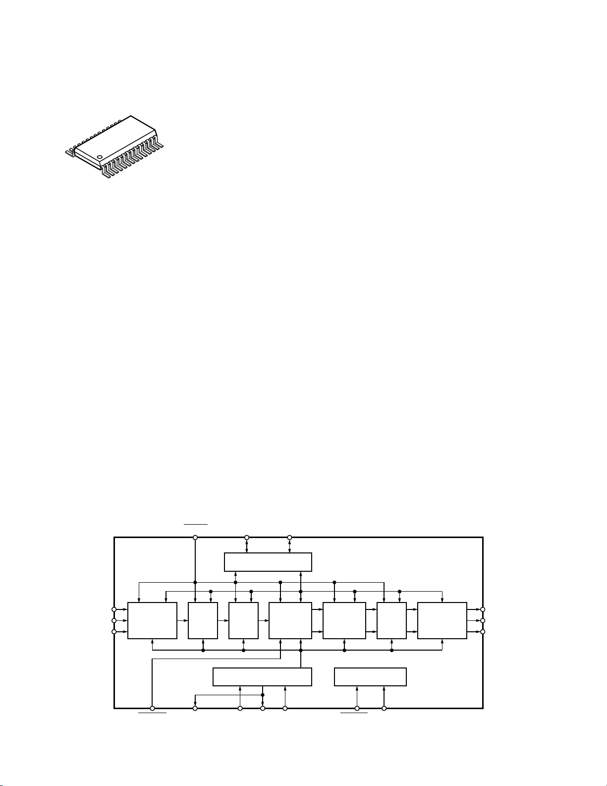
The functional STA013 chip partitioning is described in Fig. 1.
I2C CONTROL
SERIAL
INPUT
INTERFACE
BUFFER
PARSER
MPEG 2.5
LAYER III
DECODER
CORE
CHANNEL
CONFIG.&
VOLUME
CONTROL
OUTPUT
BUFFER
PCM
OUTPUT
INTERFACE
10
11
95
26
828212012 2425
34
6
7
SYSTEM & AUDIO CLOCKS
TEST INTERFACE
RESET SDA SCL
SDI
SCKR
BIT_EN
SRC INT OUT_CLK/
DATA_REQ
XTI XTO OCLK TESTEN
SCANEN
SDO
SCKT
LRCKT
Fig. 1 Block diagram: MPEG 2.5 Layer # Decoder hardware Partitioning
11
KDC-MP6090R/MP7018/MP8017
CIRCUIT DESCRIPTION (MP3)
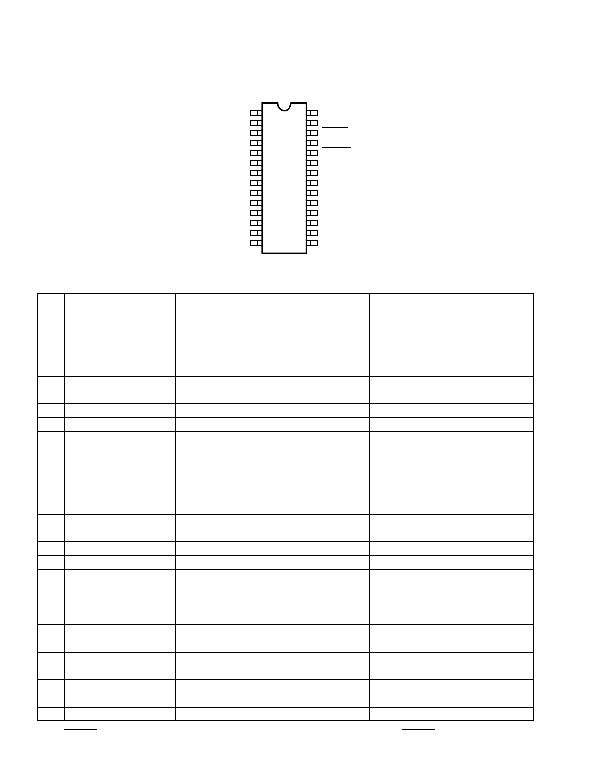
■ Pin Connection
■ Pin Description
Pin No.
Pin Name Type Function PAD Description
1 VDD_1 Supply Voltage
2 VSS_1 Ground
3 SDA I/O I2C Serial Data +Acknowledge
CMOS Input Pad Buffer
CMOS 4mA Output Drive
4 SCL I I2C Serial Clock CMOS Input pad Buffer
5 SDI1 I Receiver Serial Data CMOS Input Pad Buffer
6 SCKR I Receiver Serial Clock CMOS Input Pad Buffer
7 BIT_EN I Bit Enable CMOS Input Pad Buffer with pull up
8 SRC_INT I Interrupt Line For S.R.Control CMOS Input Pad Buffer
9 SDO O Transmitter Serial data (PCM Data) CMOS 4mA Output Drive
10 SCKT O Transmitter Serial Clock CMOS 4mA Output Drive
11 LRCKT O Transmitter Left/Right Clock CMOS 4mA Output Drive
12 OCLK I/O Oversampling Clock for DAC
CMOS Input Pad Buffer
CMOS 4mA Output Drive
13 VSS_2 Ground
14 VDD_2 Supply Voltage
15 VSS_3 Ground
16 VDD_3 Supply Voltage
17 PVDD PLL Power
18 PVSS PLL Ground
19 FILT O PLL Filter Ext. Capacitor Conn.
20 XTO O Crystal output CMOS 4mA Output Drive
21 XTI I Crystal Input (Clock Input) Specific Level Input Pad
22 VSS_4 Ground
23 VDD_4 Supply Voltage
24 TESTEN I Test Enable CMOS Input Pad Buffer with pull up
25 SCANEN I Scan Enable CMOS Input Pad Buffer
26 RESET I System Reset CMOS Input Pad Buffer with pull up
27 VSS_5 Ground
28 OUT_CLK/DATA_REQ O
Buffered Output Clock/Data Request Signal
CMOS 4mA Output Drive
Note : SRC_INT signal is used by STA013 internal sofrware in Broadcast mode only; in Multimedia mode SRC_INT must be connected to VDD.
In Functional mode TESTEN must be connected to VDD, SCANEN to ground.
1
28
OUT
_
VDD_1
VSS
BIT EN
SRC
LRCKT
VSS
VDD
SDA
SCL
SDI
SCKR
_
INT
SDO
SCKT
OCLK
2
_
1
10
11
12
13
_
2
14
_
2
27
3
26
4
25
5
24
6
23
7
22
8
21
9
20
19
18
17
16
15
CLK/DATA_REQ
VSS
_
5
RESET
SCANEN
TESTEN
_
4
VDD
_
4
VSS
XTI
XTO
FILT
PVSS
PVDD
_
3
VDD
VSS
_
3
 Loading...