Kenwood KDC-2021-SA, KDC-2021-SG Service manual

CD RECEIVER
KDC-2021SA/SG
SERVICE MANUAL
© 2001-12 PRINTED IN JAPAN
B51-7873-00 (N) 1930
The CD mechanism infomation is not in this sarvice manual.
Please, refer to sarvice manual X92-4030-0x (B51-7867-00).
Panel assy
(A64-2564-02)
KDC-2021S
COMPACT
DIGITAL AUDIO
OFF
Front glass
(B10-4141-01)
RDMLOUD REPSCAN
45W
x4
CD mechanism extension cord : W05-0618-00
Escutcheon
(B07-3054-02)
MONO
AME
ADJCLK
AUTO
AUD
DC cord
(E30-4790-05)
Mounting hardware assy
(J21-9641-13)
Plastic cabinet assy
(A02-1486-13)
Antenna adaptor
(T90-0523-05)
Lever
(D10-4589-04)x2

2
CD
IC4
IC12
IC1
POWER IC
TUNER
FM+B
AM+B
SW5V
BU5V
A8V
SERVO
CH
BACK UP
E-VOL & MPX
u-COM
BU5V
TEL-MUTE
ACC DET.
BU DET.
IC2
SW5V
E2PROM
SW5V
SERVO SW14V
IC7
IC2
IC1
PRE OUT
SP-OUT
ACC
TEL-MUTE
BACK-UP
P-CON
ANT-CONT
POWER SUPPLY
MUTE
PRE MUTE
DSIBU5V
REMOTE
SW5V
PAN DET.
PAN5V
PAN5V
LCD DRIVER
KEY MATRIX
With
ILLUM SW
A8V
CONTROL
BU5V
MARINE CN.
ANT-CON DET.
P-CON DET.
FM DET OUT
AM DET OUT
REQUEST
LO/DX
PLL-CLK
PLL-CE
S-METER
PLL-DATA
SD
MSDA
MSCLK
SW2
SW1
SW3
M MUTE
RST
STOP
LO/EJ
MO SW
RST
CH-CON
MUTE
DATA C
REQ H
DATA H
CLK
REQ C
FM
AM
CD
CH
AFS
NOISE DET
LEVEL
DATAS
MUTE
LO/DX
PLL-DATA
PLL-CLK
AFS
NOISE
S-METER
SCL
SD
SDA
PLL-CE
EN2
EN3
EN1
PC DET
PA DET
CLK
DATAL
CE
REMO
PANEL
DSI
RES
SDA
SCL
P-CON
P.ANT
FM+B
VP2
AM+B
AUDIO
ILLUM
BU5V
SW1
SW2
203mV
170mV
1200mV
1200mV
382mVK:
E:
382mVJ:
(K)
FM
(E)
(K)
(J)
(J)AM
(E)
: 1605mV
: 1276mV
: 561mV
: 1700mV
: 561mV
: 792mV
: 3529mVCD.CH
LCD
KDC-2021SA/SG
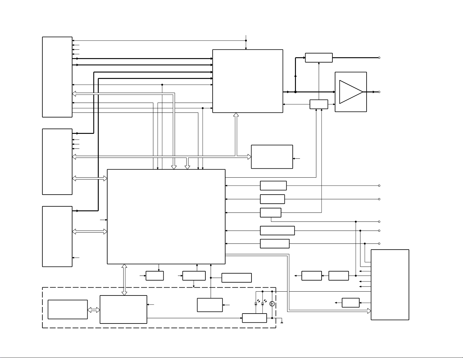
BLOCK DIAGRAM

KDC-2021 SA/SG
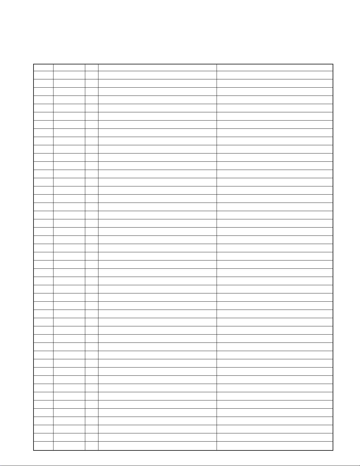
MICROCOMPUTER’S TERMINAL DESCRIPTION
SYSTEM MICROCOMPUTER uPD780058GC-XXX (IC1:X25)
Pin No. Pin Name I/O Purpose Processing in STBY Mode
1 PANEL I Panel detection Hi-Z
2 8EJE SW *1 I 8 cm disk eject end detection switch L, L when the 8 cm CD compatibility is not provided.
3 NC O Not used L
4 AVss - GND potential (for A/D and D/A) 5 L-RST O LCD driver reset
6 L-CE O LCD driver chip enable L, L is output when the panel is detached.
7 AVREF1 I 5V power supply (D/A converter reference voltage) 8 NC I Not used Hi-Z
9 PLL-DATA I/O F/E (IC3) communication data L
10 PLL-CLK O F/R (IC3) communication clock L
11 L-DATAL I LCD driver communication data (LCD) Hi-Z
12 L-DATAS O LCD driver communication data (SYSTEM) L, L is output when the panel is detached.
13 L-CLK O LCD driver communication clock H, L is output when the panel is detached.
14 R-DATA I RDS DATA Hi-Z, L when RDS is not available.
15 R-QUAL I RDS QUAL Hi-Z, L when RDS is not available.
16 CH-DATAC I 5-wire communication data (CH) Hi-Z, L when CH is not available.
17 CH-DATAH O 5-wire communication data (HEAD) L, L when CH is not available.
18 CH-CLK I/O 5-wire communication clock Hi-Z, L when CH is not available.
19 CH-REQH O 5-wire CH request (HEAD) H, L when CH is not available.
20 PLL-CE O F/E chip enable L
21 AFS O Noise detection time constant switching L
22 LO/DX O Local seek switching L
23~26 NC O Not used L
27 SD I Station detection Hi-Z
28 CH-CONT O 5-wire communication CH ON output L, L when CH is not available.
29 TYPE REF O
30 TYPE2 I Destination type setting Hi-Z
31 TYPE1 I Destination type setting Hi-Z
32 TYPE0 I Destination type setting Hi-Z
33 Vss1 34 IC2TYPE1 I Servicing pin (SEL1), normally “L” Hi-Z
35 IC2TYPE0 I Servicing pin (SEL0), normally “L” Hi-Z
36 DATA I/O IC2, CD mechanism and F/E communication data L
37 CLK O IC2, CD mechanism and F/E communication clock L
38 MUTE O Muting control output L, 15 sec. after power OFF.
39 P-MUTE O PWR IC muting output H, 15 sec. after power OFF.
40 SVR O SVR control output L
41 P-STBY O PWR IC standby output L
42 SW5V O SW5 control output “H” in 10 sec. after pow er OFF.
43 B.U-DET I B.U. detection Hi-Z
44 ACC-DET I ACC detection Hi-Z
45,46 NC O Not used L
47~49
50 BEEP O Buzzer output L
51,52
53 DSI O DSI control output L, H/L when panel is detached. FIX output is L.
PS1-0~PS1-2
PS2-0,PS2-1
Destination type and servicing setting 5V output
GND potential (for other parts than ports and analog circuitry)
O Power supply IC AUD/P.CON/P.ANT SW L
O Power supply IC ILL/AM/FM SW L
H, L when the panel is detached or with 7-segment output.
L
-
3

KDC-2021SA/SG
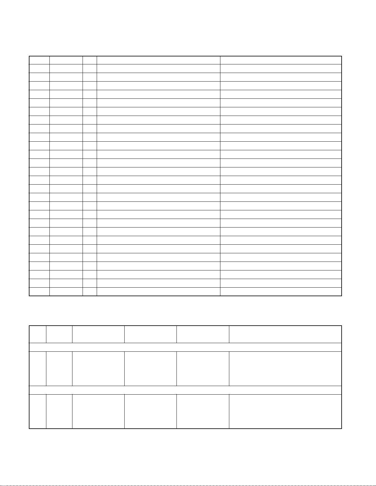
MICROCOMPUTER’S TERMINAL DESCRIPTION / ADJUSTMENT
Pin No. Pin Name I/O Purpose Processing in STBY Mode
54 LOE/LIM SW I CD mechanism Down & Limit detection Hi-Z
55 MOSW O CD mechanism motor switching L
56 LO/EJ I/O Lo/Ej switching Hi-Z
57 M-STOP O Mechanism COM stop output L
58 M-RST O Mechanism COM reset output H
59 M-MUTE I Mechanism COM mute input Hi-Z
60 RESET I System reset input Hi-Z
61 REMO I Remote control input Hi-Z
62 R-CLK I RDS CLOCK Hi-Z, L when RDS is not available.
63 CH-REQC I 5-wire CH request (CH) Hi-Z, L when CH is not available.
64 LOS SW I Loading SW detection Hi-Z
65 KEY-REQ I Key input detection Hi-Z
66 12EJE SW I 12 cm disc detection Hi-Z
67 Vss0 - GND potential (for ports) 68 VDD1 69 X2 - Main system clock oscillation 70 X1 I Main system clock oscillation 71 IC - Flash uCOM write 72 XT2 - Not used 73 XT1 - Not used (Connected to 5V power supply) 74 VDD0 - Positive power supply (for por ts) 75 AVREF0 I 5V power supply (A/D converter reference v oltage) 76 S-METER I S-meter input Hi-Z
77 PHONE I
78 NOISE I FM noise detection Hi-Z, L when RDS is not available.
79 NC O Not used L
80 AVCONT O A/D reference voltage control L
Positive power supply (for other parts than ports and analog circuitry)
Navigation muting 2.5V or more, Telephone muting 1V or less
-
. Hi-Z, L when TEL is not available.
ADJUSTMENT
No. ITEM INPUT SETTINGS
FM SECTION
98.1MHz TEST MODE : ON
1SD 0 dev FM
35dBµ (ANT input) 98.1MHz
AM SECTION
990kHz TEST MODE : ON
(1) SD 0% mod AM
35dBµ (ANT input) 990kHz
TEST MODE : ON While holding the FM key and preset “6” key, reset the unit.
TEST MODE : OFF Reset the unit.
4
TUNER (RECEIVER) ALIGNMENT
SETTINGS POINTS
Preset “1” key, and hold preset “6” k ey for a few seconds.
Preset “1” key, and hold preset “6” k ey for a few seconds.
ALIGN FOR
While holding preset “1” key, press and
preset “6” key “1111” is good.
“0000” is not good.
While holding preset “1” key, press and
preset “6” key “1111” is good.
“0000” is not good.
 Loading...