Kenwood KCAIP-500 Service manual

iPod® INTERFACE
This product uses Lead Free solder.
KCA-IP500
SERVICE MANUAL
© 2005-4 PRINTED IN JAPAN
B53-0277-00 (N) 1708
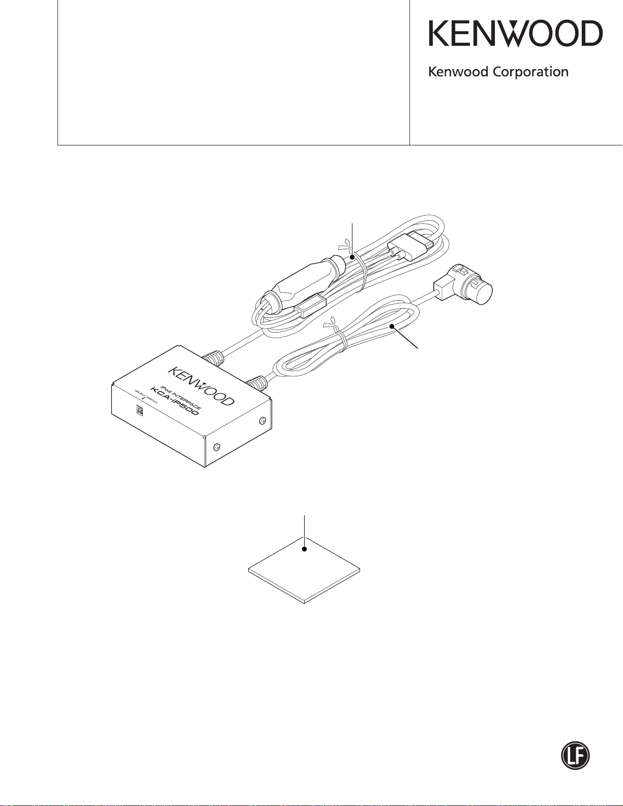
Cord with plug
(E30-6469-15)
Adhesive double-coated tape
(J69-0521-04)
Cord with DIN connector
(E30-6468-05)

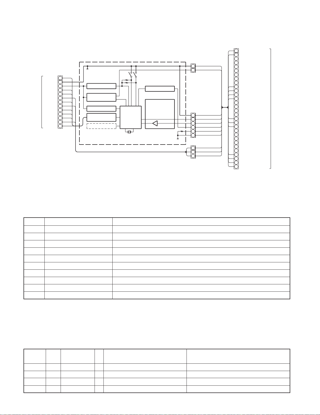
KCA-IP500
LX-BUS INTERFACE
LX DATA S
LX DATA M
LX REQ M
D GND
LX CON
LX MUTE
A GND
LX RST
Rch
LX REQ S
Lch
LX CLK
1
2
3
BU
4
5
6
7
8
9
10
11
12
13
Q1,2
BU 5V
IC4
iPod
CHARGE SW
Q3
BU DET
LX-BUS
COMMUNICATION
E2PROM
BLOCK DIAGRAM
Q7
iPod DET
IC3
IC1
SYSTEM
u-COM
12.5MHz
iPod
COMMUNICATION
INTERFACE
POWER GND
1
POWER+
2
SIGNAL WIRE GND
1
RX
2
TX
3
ACC 3.3
4
ACC TD
5
ACC DETECT
6
AUDIO-LEFT
1
AUDIO PAIR GND
2
AUDIO-RIGHT
3
iPod INTERFACE
1
F/W GND
2
F/W GND
3
TPA+
4
USB D+
5
TPA-
6
USB D-
7
TPB+
8
USB PWR
9
TPB-
10
ACCESSORY IDENTIFY
11
F/W PER+
12
F/W PER+
13
ACCESSORY PWR(3.3V)
14
RESERVED
15
USB GND
16
DGND
17
RESERVED
18
DOCK TX
19
DOCK RX
20
ACCESSORY DETECT
21
RESERVED
22
RESERVED
23
RESERVED
24
RESERVED
25
LINE-IN L
26
LINE-IN R
27
AUDIO RETURN
28
LINE-OUT L
29
LINE-OUT R
30
DGND
COMPONENTS DESCRIPTION
● CONTROL CIRCUIT UNIT (X29-4410-00)
Ref. No. Application / Function Operation / Condition / Compatibility
IC1 Communication control µ-com iPod commands and LX-BUS commands are inter-converted.
IC2 Resetting IC When voltage of BU 5V decreases to 3.6V or less, Lo is output.
IC3 Buffer 3.3V → 5V level shifter buffer
IC4 +8.5V AVR iPod re-charging DC/DC converter power supply.
Q1,2 BU 5V AVR When BU is impressed, 5V is output. Q1 and Q2 are inverted darlington connected.
Q3 BU detection SW When momentary power down and BU are detected, base is turned to Lo and Q3 goes off.
Q4 Resetting SW When system reset is turned on, base becomes Hi and Q4 is turned on.
Q5 Changer control SW When in CH CON or CH CON2 modes, base is turned to Hi and Q5 is turned on.
Q6 Changer mute SW When mute request is output to H/U, base is turned to Lo and Q6 is turned on.
Q7 iPod connection detection SW When an iPod is connected, base is turned to Hi and Q7 is turned on.
MICROCOMPUTER’S TERMINAL DESCRIPTION
● MICROCOMPUTER 30302MCP070GP (IC1 : X29)
Pin No.
1~5 N.C O Not used.
6 BYTE I External data bus switching input Connected to GND.
7HCNVSS I CNVSS Connected to GND via register.
8,9 N.C O Not used.
Active
(H/L)
Pin Name I/O Application Processing / Operation / Description
2

KCA-IP500
MICROCOMPUTER’S TERMINAL DESCRIPTION
Pin No.
10 H LX_RST I Hard-resetting to the slave unit H : Normal, L : Reset
10 L RESET I Reset input Reset IC or LX_RST input, H : Normal, L : Reset
11 XOUT O Main clock output Connected to Ceralock resonator (12.5MHz)
12 VSS I Power supply input Connected to GND
13 XIN I Main clock input Connected to Ceralock resonator (12.5MHz)
14 VCC1 I Power supply input Connected to B.U 5V
15 NMI I NMI interruption input Connected to B.U 5V via register.
16 L BU_DET I Momentary power down detection B.U voltage detection, H : When down, L : Normal
17 L LX_CON I Startup request to the slave unit H : Slave unit OFF, L : Slave unit ON
18 LX_REQ_M I Communication request to the slave unit
19 N.C O Not used.
20 H LX_MUTE O Mute request from slave unit L : Mute ON, H : Mute OFF
21 H Charger Con O iPOD recharging control H : iPod re-charging power supply circuit ON
22~26 N.C O Not used.
27 DATAI I Data from iPOD
28 DATAG O Data to iPOD
29 LX_DATA_S O Data from slave unit
30 LX_DATA_M I Data to slave unit
31 LX_CLK I LX BUS clock
32 LX_REQ_S O Communication request from slave unit
33 ROM_SDA I/O ROM correction E2PROM data
34 ROM_SCL I/O ROM correction E2PROM clock
35 H ROM_WR I
36~38 N.C O Not used.
39 L FLASH_EPM I µ-com flash EPM Connected to GND via register.
40~43 N.C O Not used.
44 H FLASH_CE I µ-com flash CE Connected to B.U 5V via register.
45~59 N.C O Not used.
60 VCC2 I Power supply input Connected to B.U 5V.
61 TEST I Test mode setting L : Test mode, H : Normal
62 VSS I Power supply input Connected to GND.
63~71 N.C O Not used.
72 L iPOD_DET I iPOD connection detection
73~84 N.C O Not used.
85,86 L SW1, SW2 O Switch for mode switching Connection unit recognition SW
87~93 N.C O Not used.
94 AVSS I Analog power supply input Connected to GND.
95 N.C O Not used.
96 VREF I Reference voltage input Connected to GND.
97 AVCC I Analog power supply input Connected to B.U 5V.
98~100 N.C O Not used.
Active
(H/L)
Pin Name I/O Application Processing / Operation / Description
iPod re-charging power supply circuit control
L : iPod re-charging power supply circuit OFF
ROM correction E2PROM write mode EEPROM write recognition terminal
setting H : EEPROM write, L : Normal
iPod connection detection
H : iPod not connected, L : iPod connected
3
 Loading...