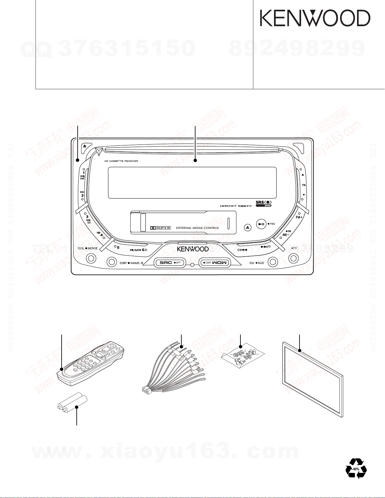
CD CASSETTE RECEIVER
DP X-30 70
Q
Q
3
7
6
3
1
5
1
5
0
DP X-30 70B
SERVICE MANUAL
PANEL
DPX-3070
DPX-3070B : (A64-3557-08)
TEL 13942296513 QQ 376315150 892498299
: (A64-3562-08)
FRONT GLASS ASSY
DPX-3070
DPX-3070B : (B10-4673-08)
: (B10-4676-08)
8
4
2
9
© 2004-7 PRINTED IN JAPAN
B53-0188-00 (N) 378
9
8
2
9
9
TEL 13942296513 QQ 376315150 892498299
TEL
REMOTE CONTROLLER ASSY (RC-505)
(A70-2059-05)
13942296513
BATTERY
(Not supplied)
Q
Q
DC CORD ASSY
(E30-6405-08)
6
7
3
SCREW SET
(N99-1724-05)
3
1
5
1
9
8
0
5
ESCUTCHEON ASSY
(B07-3046-04)
2
4
9
8
2
9
9
w
w
w
.
xia
o
y
u
1
6
3
.
c
o
m
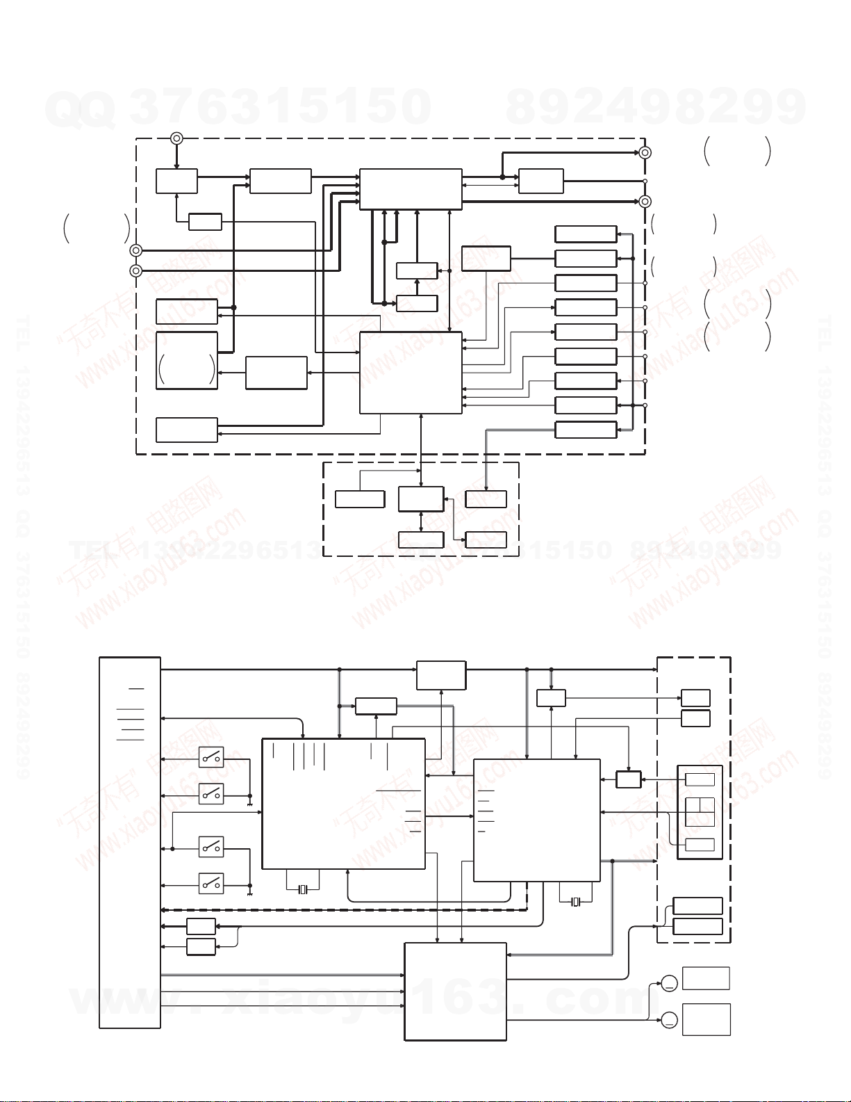
DP X-30 70/30 70B
BLOCK DIAGRAM
7
Q
DPX-04
DPX-3070
DPX-MP4070
Q
3
TU221 IC301
AUX IN
CD CH
TEL 13942296513 QQ 376315150 892498299
6
ANT
TUNER
IC12
PLL
MD MECHA
(DPX-05MD)
CASSETTE
MECHA
DPX-04
DPX-3070
DPX-MP4070
CD MECHA
1
3
INPUT
SELECTOR
IC351
CASSETTE
MECHA
DRIVE
CONTROL UNIT
5
1
IC101
IC1
IC921
REMOTE
5
0
MAIN UNIT
E. V OL
BASS/TRE/FADER
REAR
N-FAD
FRONT
IC103
WOW
-12.7dB
MAIN u-COM
IC901
LCD
DRIVER
IC2
SYSTEM
RESET
LED
8
IC601
POWER
AMP
9
2
AUDIO 8V
BU 5V
LINE MUTE
ANT CONT
P. CONT
ILLUMI
ACC DET
BU DET
LED 11V
4
8
9
PRE OUT
(FRONT)
SP OUT
PRE OUT
(REAR/N-FAD)
DPX-3070
DPX-MP4070
DPX-3070
DPX-MP4070
LINE MUTE
ANT CONT
P. CONT
ILLUMI
ACC
BU
2
9
DPX-05MD
DPX-3070
DPX-MP4070
DPX-05MD
DPX-3070
DPX-MP4070
DPX-05MD
DPX-3070
DPX-MP4070
9
TEL 13942296513 QQ 376315150 892498299
TEL
CD PLAYER UNIT (X32-5490-01)
w
13942296513
BU5V 15
DGND 14
CLK1819
DATA
MUTER
13
MUTEL 12
MRST 11
MSTOP
LOS SW 20
12EJE SW
LOE&LIM
SW
8EJE SW 17
A8V 9
DOUT
Lch 8
AGND 7
Rch226
S7.5V 3
SGND
LO/EJ 5
w
w
NC 16
10
21
1
OPEN
2
4MOTOR
OPEN
S1(LOS SW)
S2(12EJE SW)
S3
(LOE & LIM SW)
S4(8EJE SW)
LPF
LPF
.
xia
IC1
CLK
LOE & LIM
SW
S7.5V
BU5V
DATA
MUTER
MECHANISM
CONTROL IC
X1
4.19MHz
o
MRST
MUTEL
MSTOP
y
Q2
5V SW
Z MUTE L
Z MUTE R
Q
PON
PON
SERCH
INTQ
DSP RESET
SCK
DRV MUTE
IC4
u
Q
IC2
3.3V AVR
SW5V
SI
AO
STB
SO
CNT
LO/EJ
1
CNTL
MUTE
4ch BTL
DRIVER
6
3
FDIN-
TDIN-
KEYLCD
7
SW3.3V
IC3
INTQ
SO
RST
AO
STB
SCK
SI
FD+
TD+
SD+
MD+
SPIN-
SLIN+
3
3
6
CD RF/SERVO/
DSP/DAC IC
LZM
BIAS
TR+
TR-
FO+
FO-
SPD+
.
SPD-
SLD+
SLD-
RZM
1
TX
5
Q3
APC
LOUT
c
1
LD
PRE OUT
ROUT
X2
16.934MHz
0
5
PD
F
A
B
C
D
E
o
9
8
Q4
SW
VREF
m
8
9
4
2
DPU1 :
OPTICAL PICKUP
LD
PD
F
AB
C
E
TR COIL
FO COIL
DM1
SPINDLE
M
MOTOR
DM2
LOADING
M
& SLED
MOTOR
2
9
9
2

DP X-30 70/3070B
COMPONENTS DESCRIPTION
7
Q
Q
● MAIN UNIT
TEL 13942296513 QQ 376315150 892498299
TEL
w
3
Ref. No. Application / Function Operation / Condition
IC1 MAIN µ-COM Main microcomputer
IC2 RESET
IC3 MUTE
IC4 ROM COLLECTION
IC5 SECURITY ROM
IC12 PLL PLL for tuner
IC101 E-VOL Electric volume
IC103 WOW
IC104 WOW FOCUS
IC301 AUDIO SELECTOR
IC351
IC601 POWER IC Output amplifier
Q1 RESET SW
Q5 FM VCC SW
Q101 E-VOL MUTE SW
Q141 WOW FOCUS SW
Q221 FM/AM VT DRIVER
Q271,272 PRE MUTE DRIVER Mute switch for preout
Q277 PRE MUTE SW
Q281,282 PRE MUTE DRIVER Mute switch for preout
Q287 PRE MUTE SW
Q802~805
Q806,807 P-ANT SW
Q808
Q809 BACK-UP DET SW
Q810 ACC DET SW
Q811 ILLUMI DET SW
Q812
Q813 BACK-UP DET SW
Q851 P. ON SW
Q852~854
Q855,856 D5V A VR
Q857,858 BU5V AVR
Q859 SW5V SW
Q860 SW5V DRIVER
w
CASSETTE MOTOR DRIVER
13942296513
P. CON SW (P-ANT SW)
POWER IC STANDBY SW
BMS CONTROL DRIVER
S7.5V AVR
w
6
.
xia
3
1
5
1
Audio switch for cassette
and tuner
Driver for cassette motor
External amplifier driver
7.5V power supply for
CD mechanism
5V power supply for
CD mechanism
o
y
5
u
0
Q
Q
1
Ref. No. Application/Function Operation/Condition
Q861,862 MOTOR+B SW
Q863,864 A8V AVR
Q865 P. ON-ILULMI SW
Q866,867 LED11V AVR
Q868,869 MAIN MOTOR+B SW
Q870 P. ON SW
● CONTROL UNIT
Ref. No. Application/Function Operation/Condition
IC901 LCD DRIVER LCD driver
IC921 REMOTE Receives remote signal
Q903 RED LED SW
Q904 BLUE LED SW
Q905 GREEN LED SW
Q906
Q921 REMOTE SW
7
3
● EQUALIZER UNIT
Ref. No. Application/Function Operation/Condition
IC250 DOLBY/EQUALIZER Cassette audio equalizer
● CD PLAYER UNIT (X32-5490-01)
Ref. No. Application/Function Operation/Condition
IC1
IC2 SW3.3V AVR
IC3
IC4 4ch BTL DRIVER coil, spindle motor and
Q2 SW 5V Switch for SW5V.
Q3
Q4 SW For switching equalizer.
6
3
4
2
9
8
SECURITY INDICATOR SW
8
0
5
1
5
1
3
6
MECHANISM Activates when BU5 and
CONTROL IC
CD RF/SERVO/ Activates when SW3.3V
DSP/DAC IC goes “H”.
AUTOMATIC POWER
CONTROL
.
c
o
m
8
9
Power supply for
cassette motor
8V power supply for audio
11V power supply for LED
Power supply for
cassette main motor
9
4
2
9
MSTOP (Pin No.12) goes “H”.
Activates when CNTL
(Pin No.1) goes “H”.
Focusing coil, tracking
sled motor driver.
LD driver.
2
8
9
2
9
9
TEL 13942296513 QQ 376315150 892498299
9
3

DP X-30 70/30 70B
MICROCOMPUTER’S TERMINAL DESCRIPTION
7
Q
Q
● MAIN µ-COM : MN101C49KWG (MAIN UNIT : IC1)
Pin No.
1 VREF- - µ-com reference voltage (–)
2 REEL S I Cassette mechanism reel rotation detection
3 REEL T I Cassette mechanism reel rotation detection
4 DC ERR I Power IC offset voltage observation
5 LINE MUTE I Line mute detection
TEL 13942296513 QQ 376315150 892498299
6HACC DET I ACC power supply detection H : ACC OFF
7LILLUMI DET I Dimmer illumination detection L : ILUMMI ON
8 JS1 I Destination setting 3
9 CD MECHA SEL I CD mechanism selection terminal
10 VREF+ - µ-com reference voltage (+)
11 VDD - Power supply for µ-com
12 OSC2 - Main clock output
13 OSC1 - Main clock input
14 VSS - GND for µ-com
15 XI - Sub clock input
16 XO - Sub clock output
TEL
17 MMOD - Memory mode setting
18 LX DATA M O Data to slave unit
19 LX DATA S I Data from slave unit
20 LX CLK I/O LX BUS clock
21 L MODE1 I Cassette mechanism condition detection SW1 H : Normal condition, L : Reset
22 L MODE2 I Cassette mechanism condition detection SW2
23 MODE3 I Cassette mechanism condition detection SW3
24 PWIC BEEP O Beep output
25 NC 26 BU DET I Momentary power down detection
27 LX REQ S I Communication request from slave unit
28 REMO I Remote control signal input Pulse width detection
29 L DATA IN I Data input from LCD driver
30, 31 NC 32 VDD2 - Power supply for µ-com
33 NRST - µ-com reset terminal L : Reset
34 LCD BLIGHT R O LCD back light control (Red) PWM control
35 NC 36 LCD BLIGHT B O LCD back light control (Blue) PWM control
37 NC -
w
38 L INH O Turns off LCD display
3
Active
(H/L)
13942296513
w
w
6
Pin Name I/O Application Processing Operation
.
xia
3
1
5
o
1
y
5
u
0
Q
Q
1
3
6
7
3
6
4
2
9
8
H : MP3 CD mechanism
L : NORMAL CD mechanism
8
0
5
1
5
1
3
L : Normal condition, H : Momentary power down
.
c
o
m
9
9
8
2
4
2
9
8
9
2
9
9
TEL 13942296513 QQ 376315150 892498299
9
4

DP X-30 70/3070B
MICROCOMPUTER’S TERMINAL DESCRIPTION
7
Q
Q
Pin No.
TEL 13942296513 QQ 376315150 892498299
TEL
w
3
Active
(H/L)
39 L CE O Data latch to LCD driver
40 LCD BLIGHT G O LCD back light control (Green) PWM control
41 VPP - Power supply terminal for flash memory writing
42 L DATA OUT O Data output terminal to LCD driver
43 L DATA IN I Data input from LCD driver
44 L CLK O Clock output terminal to LCD driver
45 SDA I/O E2PROM writing terminal
46 NC 47 SCL I/O CD mechanism I2C clock output terminal
48 ROMCOL WR I
49 LED SI O LED control for security indicator
50 JS2 I Destination setting 4
51 TUN TYPE1 I Destination setting 2
52 TUN TYPE0 I Destination setting 1
53 SUB M+ O Cassette mechanism sub motor control
54 SUB M- O Cassette mechanism sub motor control
55 MS IN I Between-numbers detection signal input L : Number exists
56 H DOLBY O DOLBY NR H : DOLBY NR ON
57 H C MUTE O Equalizer mute H : MUTE ON
58 L METAL O Play-back equalizer switch L : METAL ON
59 C F/R O Head input switch L : Forward, H : Reverse
60 MS MODE O Detection sensitivity switch L : G1, H : G2
61 TUN CE O Tuner PLL data setting (CS)
62 TUN DI I Tuner PLL data setting (DATA IN)
63 TUN DO O Tuner PLL data setting (DATA OUT)
64 TUN CLK O Tuner PLL data setting (CLOCK)
65 SD/ST-IND I Front-end S-meter input
66 CD DISC12 SW I CD disk detection terminal (12cm)
67 CD LOS SW I CD loading detection terminal
68 CD MUTE R I CD mute (Rch) request terminal L : Rch mute request
69 CD MUTE L I CD mute (Lch) request terminal L : Lch mute request
70 L CD MRST O CD mechanism µ-com reset terminal H : Normal condition, L : Reset
71 L CD MSTOP O CD mechanism µ-com stop terminal
72 CD DISC8 SW I CD disk detection terminal (8cm)
73 CD LOE LIM SW I CD detection terminal (Chucking switch) H : Loading completes, L : No disk
74 CD LOEJ O CD motor control terminal
13942296513
w
w
6
Pin Name I/O Application Processing Operation
.
xia
3
1
5
1
5
0
Presence-or-absence setting for ROM collection
(E2PROM)
Q
Q
o
y
u
1
6
3
7
3
6
8
3
.
4
2
9
8
0
5
1
5
1
During seek operation, H: Number exists
During reception, H : Mono, L : Stereo
H : Mechanism µ-com activates
L : Mechanism µ-com stops
c
o
m
9
9
8
2
4
2
9
8
9
2
9
9
TEL 13942296513 QQ 376315150 892498299
9
5
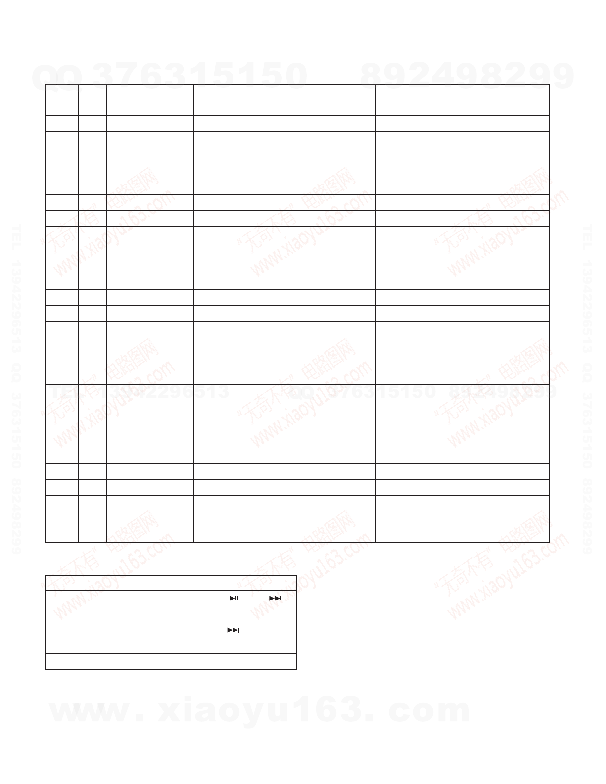
DP X-30 70/30 70B
MICROCOMPUTER’S TERMINAL DESCRIPTION
7
Q
Q
Pin No.
75 CD MOTOR O CD motor control terminal
76 L SW MUTE O Mute control for switch During mute : L
77 NC 78 L PWIC STBY O Power IC standby control
79 L PWIC MUTE O Power IC mute control During momentary power down : H
80 ES SW O X’over filter select terminal 3
TEL 13942296513 QQ 376315150 892498299
81 ES SEL2 O X’over filter select terminal 2
82 ES SEL1 O X’over filter select terminal 1
83 H AUD MUTE O Audio mute control terminal H : MUTE ON
84 WOW MODE3 O WOW IC control terminal 3
85 WOW MODE2 O WOW IC control terminal 2
86 WOW MODE1 O WOW IC control terminal 1
87 WOW Focus O WOW IC control terminal 4
88 SRC SEL1 O IC2-5 input source switch
89 BMS CTRL O External amplifier control
90 H PON ILL O Key illumination control (Flash EPM) H : ON
91 MOTOR+B O Cassette mechanism main motor control
TEL
92 H P ANT O
93 H P CON O External amplifier current control H : ON
94 L MUTE ACOUT O Mute on ACOUNT line L : MUTE
95 DAVSS - GND for µ-com
96 H PON O Power supply control H : ON
97 SW5V O SW 5V control H : ON
98 H LX CON O Start-up request to slave unit H : SLAVE UNIT ON, L : SLAVE UNIT OFF
99 LX REQ M O Communication request to slave unit
100 DAVDD - Power supply for µ-com
3
Active
(H/L)
13942296513
6
Pin Name I/O Application Processing Operation
3
1
5
1
5
Power antenna control terminal
(When P. CON is Hi only)
0
Q
Q
3
7
6
2
9
8
5
1
5
1
3
H : ANT ON, L : ANT OFF
4
0
9
8
9
8
2
4
2
9
8
9
2
9
9
TEL 13942296513 QQ 376315150 892498299
9
● KEY MATRIX TABLE
KS1 KS2 KS3 KS4 KS5
KI1 3 VOL+
LI2 2 VOL- SRC FM
KI3 1 ATT AM
KI4 WOW 4 5 CD EJ RESET
KI5 EQ 6 TAPE EJ DISP
• Multiple push
Frequency step switch (K/M destination) : 1 + 5 + SRC
After-sales service test mode in assembly line : ATT + WOW + SRC
w
w
w
DC offset forced clear : DISP + EQ + SRC
6
.
xia
o
y
u
1
6
3
.
c
o
m

DP X-30 70/3070B
MICROCOMPUTER’S TERMINAL DESCRIPTION
7
Q
Q
● CD MECHANISM CONTROL IC : 789166YGB-A513 (X32 : IC1)
Pin No. Name I/O Description Processing Operation
TEL 13942296513 QQ 376315150 892498299
TEL
w
3
1~6 NC I NC GND
7 ZMUTE L I 0-bit MUTE detect (Lch)
8 ZMUTE R I 0-bit MUTE detect (Rch)
9AVSS - DGND
10 /MUTE L O Lch Audio mute control L : MUTE ON, H : MUTE OFF
11 /MUTE R O Rch Audio mute control L : MUTE ON, H : MUTE OFF
12 /MSTOP I Interruption for stand-by L : Stop, H : Release for stop mode
13 INTQ I Interruption for DSP IC H : Interruption
14 /FOGUP I Interruption for focus gain up
15 PON O Power ON/OFF control H : ON, L : OFF
16 /SCK O Serial data clock output for DSP
17 VDD1 - BU5V
18 SO O Serial data output for DSP
19 SI I Serial data input for DSP
20 /CLK I/O I2C clock for system control
21 DATA I/O I2C data for system control
22 VPP - Flash saving terminal
23 XT2 - NC Open
24 XT1 I NC GND
25 /MRESET I Reset detect L : Reset, H : Normal condition
26 X2 - System clock 4.19MHz
27 X1 I System clock 4.19MHz
28 VSS0 - DGND
29 VDD0 - BU5V
30 LOE&LIM SW I Loading end & limit SW detect L : Inside detect, H : Outside
31 DRV MUTE O Driver muting L : MUTE ON, H : MUTE OFF
32,33 NC O NC Open
34 /SERCH O Condition of serch state L : Search, H : Normal condition
35 /STB O Data strobe signal output
36 A0 O Command & parameter signal output
37 VSS1 - DGND
38 /DSP RESET O DSP reset control L : Reset, H : Normal condition
39~41 NC - NC Open
42 /PON O Power ON/OFF control L : ON, H : OFF
43 AVDD - BU5V
44 AVREF - BU5V
13942296513
w
w
6
.
xia
3
1
5
o
1
y
5
u
0
Q
Q
1
3
6
7
3
6
4
2
9
8
Less than 54h : Normal condition,
More than 54h : 0-bit mute detect
Less than 54h : Normal condition,
More than 54h : 0-bit mute detect
L : Foucus gain up, H : Normal condition
0
5
1
5
1
3
.
c
o
9
9
8
m
8
2
4
2
9
8
9
2
9
9
TEL 13942296513 QQ 376315150 892498299
9
7
DP X-30 70/30 70B
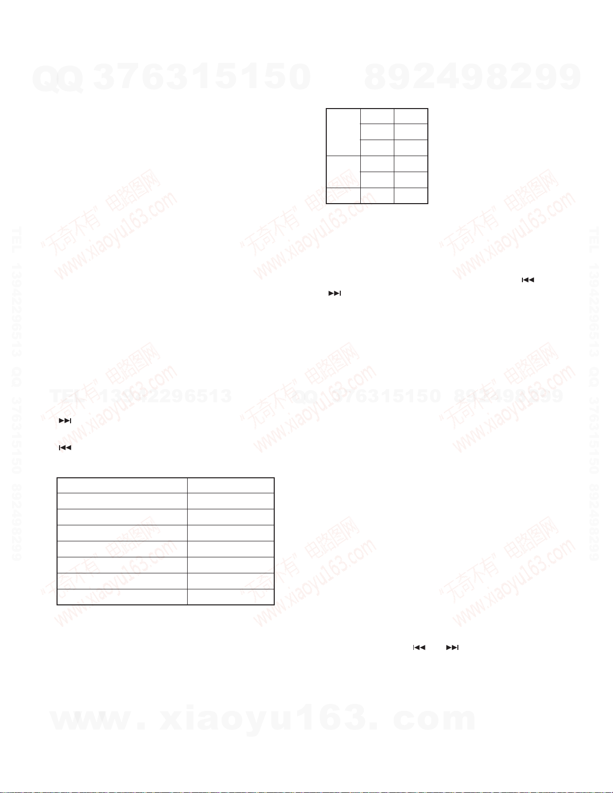
TEST MODE
7
Q
Q
● How to enter the test mode
• In order to enter the test mode, while pressing down [ATT]
+ [WOW] keys simultaneously, press [SRC] key.
● Test mode conditions
• The test mode starts up when ST ANDBY source is selected.
• The volume value is –10dB. (30 on the display)
• Beep prohibited.
• All lights displayed. (3-color LED lights up for all three col-
TEL 13942296513 QQ 376315150 892498299
ors. (white lighting))
• WOW : OFF
• EQ : Natural
● Test mode (Source : CD)
• When starting disc loading, tracks will be played starting
with the Track No. 9.
• The key operations below will be conducted only when the
source is CD.
Even when changes occur in the track number being pla yed
with the other sources, the play condition will persist.
TEL
•[ ] key is to be used for selecting preset tr ac ks only. (Refer to the table below.)
•[ ] key is to be used for down selection, as with regular
operation.
3
Preset [1] key for Track No. 19
Preset [2] key for Track No. 5
Preset [3] key for Track No. 15
Preset [4] key for Track No. 14
No. 1~No. 8, No. 14, No. 16~Max No. 9
13942296513
Current track Track to be searched
No. 9 No. 15
No. 15 No. 10
No. 10 No. 11
No. 11 No. 12
No. 12 No. 13
No. 13 No. 14
6
3
1
5
1
5
0
• The settings for Q, Feq, and Ex are fixed.
Bass Feq 150Hz
Mid
Treble Feq 10kHz
● Test mode (Audio adjustment)
• While the source is being displayed, long-clicking on the
[EQ/AUD] k ey will cause the unit to enter Adjustment Mode.
By toggling on the [FM] and [AM] key, the items below can
be selected and adjustments can be made with [
[
] keys.
The balance adjustment is set for three steps
: RIGHT ↔ CENTER ↔ LEFT (L15, R15)
The fader adjustment is set for three steps
: FRONT ↔ CENTER ↔ REAR (F15 and R15)
● Test mode (DC offset detection)
• When DC error detection is carried out during the Test Mode,
7
3
Q
Q
the unit shuts down without writing the error information to
the EEPROM. The other cases will be the same as the DC
offset specifications.
● Test mode (Display of DC offset detection results)
• When in this mode, the mode for “Display of DC offset detection results” will be added in the MENU items at the time
when Test Mode Standby is the source. This will make it
possible to confirm results with presence-or-absence detection.
MENU selection : DIMMER adjustment → … → (NAVI ATT
ON/OFF) → (CODE STBY) → Display of DC offset detection results
• Display
DC offset detected : DC Err
DC offset not detected : DC OK
9
8
Q 2.0
Ext ON
Q 2.0
Feq 1kHz
1
3
6
5
1
2
5
4
0
9
8
9
8
2
4
2
9
8
9
] and
2
9
9
TEL 13942296513 QQ 376315150 892498299
9
● Test mode (EQ adjustment)
• While the source is being displayed, clicking once on the
[EQ/AUD] k ey will cause the unit to enter Adjustment Mode.
When [1] key is pressed: Flat
When [2] key is pressed : Full-boost
When [3] key is pressed : Full-cut
w
w
w
8
.
xia
o
y
u
✳ The detection information in the EEPROM can be forcibly
1
cleared by pressing [
seconds while the DC offset detection (DC Err) is being
displayed. In this case, the display will be for DC offset not
detected. (DC OK).
6
3
.
c
] or [ ] key for more than two
o
m
TEST MODE
DP X-30 70/3070B
7
Q
Q
● Test mode (Accumulated elapse time display)
• When in this mode, the mode for “Accumulated Elapse Time
• MENU selection: DIMMER adjustment → … → (NAVI ATT
TEL 13942296513 QQ 376315150 892498299
✳ By pressing [ ] or [ ] key for during Accumulated Elapse
● Releasing the test mode
• The Test Mode is released by the following sequence: Re-
3
Display” will be added in the MENU items at the time when
Test Mode Standby is the source. This will make it possible
to confirm on the accumulated elapse time.
ON/OFF) → (CODE STBY) → Display of DC offset detection results → Accumulated Elapse Time Display
Time Display, the sources for the accumulation can be
switched. (Repeating sequence : TAPE accumulation time
→ CD accumulation time → TAPE accumulation time)
set, ACC OFF and ON, Power OFF and ON. Also, by ACC
OFF and POWER OFF, the Source of Tuner and Audio will
go into the initial conditions.
6
3
1
5
1
5
0
● Coping with backup current measurement
• Regardless of the Test Mode, when reset in the ACC OFF
state (backup ON), MUTE will be OFF after two seconds.
(The power for peripherals will not be turned OFF until the
CD mechanism stops. This will take two seconds plus.)
● Forced clearing of DC offset detection
• Regardless of the Test Mode, when power is turned on by
[SRC] key while depressing the following keys. This will be
the forced clearing of DC Err condition in the EEPOM. This
will clear the data in the EEPROM even in the case where
there is no error data.
• Key Operation
Press the [SRC] key while pressing the [DISP] and [EQ]
key at the same time.
8
9
2
4
9
8
2
9
9
TEL 13942296513 QQ 376315150 892498299
TEL
13942296513
Q
Q
3
7
6
3
1
5
1
5
0
8
9
ADJUSTMENT
BALANCE/FADER/BASS/TREBLE : CENTER
METAL/DOLBY NR : OFF
No. ITEM
CASSETTE DECK SECTION
DOLBY Connect an AC voltmeter between (EQUALIZER UNIT)
1 (PLAY BACK TCC-130 TAL (TP25) and TAG (GND), TAPE PLAY VR250A (L) 388mV
LEVEL) also between VR250B (R)
INPUT
OUTPUT SETTINGS
SETTINGS SETTINGS POINTS
(FOIL SIDE VIEW of MAIN UNIT)
TAR (TP24) and TAG (GND).
RECEIVER ALIGNMENT
2
8
9
4
2
ALIGN FOR FIG.
9
9
w
w
w
.
xia
o
y
u
1
6
3
.
c
o
m
9
A B C D E
3
Q277
C
DPX-3070/3070B
1
2
TEL 13942296513 QQ 376315150 892498299
3
4
5
6
7
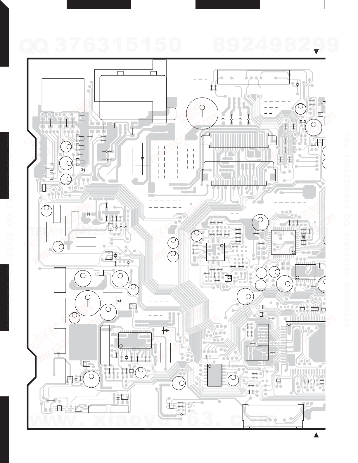
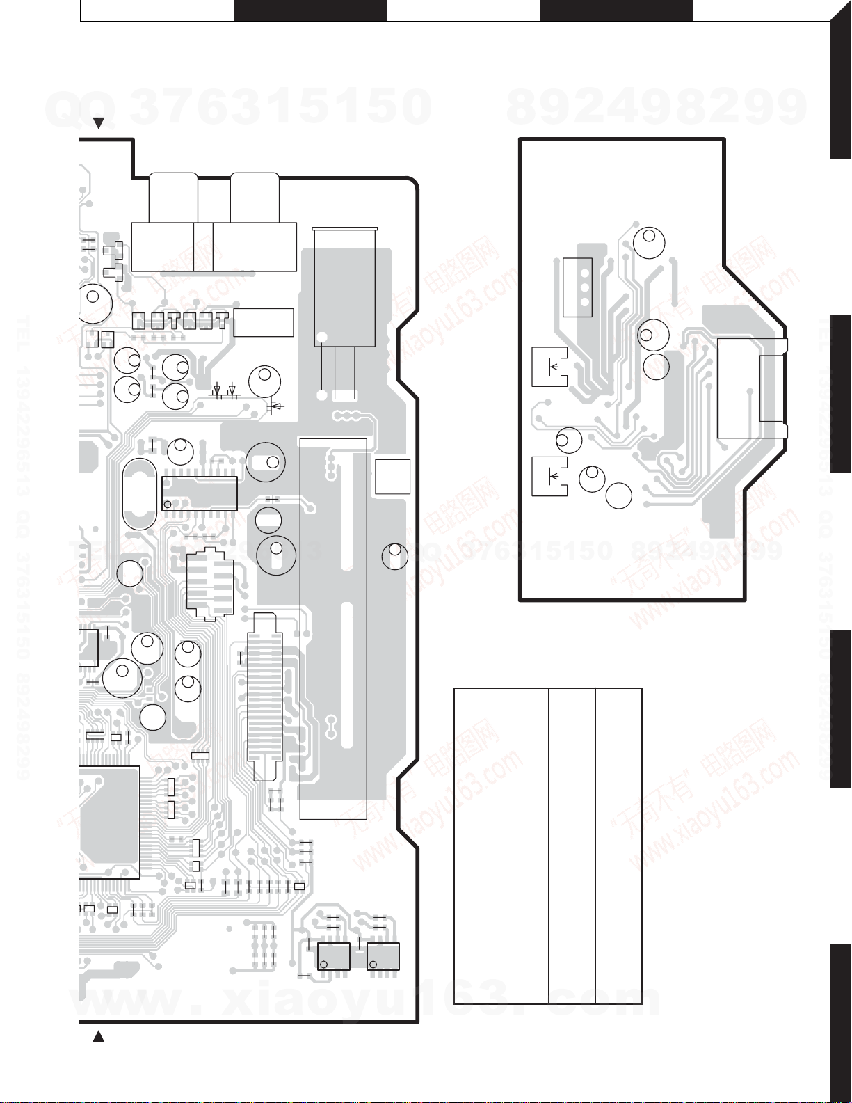
PC BOARD (COMPONENT SIDE VIEW)
Q
MAIN UNIT
TEL
w
Q
R211
D205
D206
C803
R856
w
7
3
CN201
13
12
11
8
10
9
R209
R210
C209
C207
RN201
C206
EB
Q805
R808
13942296513
C802
EB EB EB EB
Q864
Q858
Q853
Q854
R855
E
C
B
B
C
E
Q851
w
4
756
R807
R206
EB
Q852
R859
3
6
2
1
R202
C202
R212
D203
D204
C201
D201
D207
Q807
D802
BE
R803
R804
C860
C856
Q855
EB
C853
D814
C852
Q868
EB
EBEEBB
.
R827
C855
R865
Q869
xia
1
3
89
R824
R830
C808
C805
D804
D806
R809
R813
R805
Q813
EB
Q812
BE
E
C
B
B
C
E
Q870
R857
111
210
CN351
R356
R353
R354
C357
C358
R812
D809
D813
R828
R360
R359
R355
D816
Q862
C807
R826
R829
C858
25
1
C356
R811
D808
C830
D820
R357
R358
C359
5
R820
R821
R817
D811
D812
C862
EB
Q859
IC351
C355
D351
RN351
Q861
o
1
116
D801
C865
C354
C352
y
CN801
14
13
C351
C360
5
L801
JW16
JW15
C353
JW14
JW17
JW3
JW7
C153
C154
R351
u
0
Q
D352
R352
E
B
C
Q865
1
JW9
Q
C864
C
R863
B
R864
E
C863
D819
C801
JW18
EB
6
JW19
C146
3
C148
R149
JW6
C151
R152
Q866
8
JW8
R143
7
2413
C155
R150
3
1
R629
R632
24
22
R144
R148
C144
C145
3
6
R146
R147
12 25
IC103
R155
R153
R156
R151
R154
JW20
JW1
RN18
17
IC3
.
9
2
D614
D613
CN291
CN292
JW24
C143
C141
C142
R142
R141
5
1
C164
R145
1
C163
48 37
C162
C161
C158
36
C157
45
1
Q141
8
C156
IC104
14 8
C9
c
1
R157
R159
EB
R158
2
D612
5
R164
R162
R160
R161
R163
C1
R1R2
R9
R13
o
D611
0
C109
C110
C111
C112
C4
16
4
C108
C115
BP
R3R4
R8
RN3
15
9
JW23
JW22
1
1
C101
23 33
8
C116
BP
RN17
RN1
R5
X2
X1
C5
R10
m
8
27
26
JW2
C604
C602
C601
C603
JW5
C107
22
4
2
9
IC101
34
C308
C117
R6
R7
CN1
C309
C303
R54R55
125
26100
RN4
IC601
C623
C612
C614
C613
C611
R104
12
9
44
1
2
2
D601
D602
R625
R103
C106
R102
R101
8
111
20
1
RN16
R56
R630
R622
R623
C105
2
D101
C102
C103
IC301
R37
IC1
RN6
9
D281
EB
Q287
C104
9
1011
R308
RN15
RN5
9
D28
C622
TEL 13942296513 QQ 376315150 892498299
EB
C284
9
C302
RN14
RN7
10
JIHGF
VR250B
C259B
VR250A
C262B
BP
C257
C262A
C259A
BP
C260
1
24
5
210
19
CN250
CN251
EQUALIZER UNIT
DPX-3070/3070B
1
7
D283
D281
EB
Q287
C284
C302
1011
RN15
RN7
w
3
CN271B
Q282
Q281
C622
Q277
R870
R869
C283
X201
13942296513
C374
BP
C301
R313
RN14
R34
75 51
5076
R21
R23
R20
w
Q
Q
R630
R622
TEL 13942296513 QQ 376315150 892498299
C104
TEL
101
102
103
R308
RN5
w
L231
D284
R287R278R277
C273
20
1
R238
C304
C373
BP
R30
Q272
EBEBEBEB EB
RN13
RN12
RN9
RN8
6
D274
Q271
C274
D333
C231
C239
IC12
R239
CN301
91
C242
C243
RN11
RN10
R53
.
xia
1
3
CN271A
13
CN331
C332
D332
D331
C236
11
R236
10
C234
BP
C221
102
C372
CN371
C371
R372
R14
R18
R15
L4
L5
R27
R29
R24
R26
R28
R371
R12
R25
122
R11
5
DSP221
R44
R45
R373
RN2
C6
R41
o
1
ANT221
18981
TU221
R43
R42
8
54
IC4
C7
1
y
5
L221
R52
R51
8
IC5
1
u
0
C223
5
4
Q
Q
1
6
4
2
9
8
8
0
5
1
5
1
3
6
7
3
MAIN UNIT
Ref. No. Address
IC1 6E
IC3 6D
IC5 7G
IC12 4F
IC101 4E
IC103 4D
IC104 5D
IC301 5E
IC351 6C
IC601 2E
Q141 5D
Q271 2F
Q272 2F
Q277 3F
Q281 2F
Q282 2F
Q287 3E
Q805 4A
3
Refer to the schematic diagram for the values of
resistors and capacitors.
.
Ref. No. Address
Q807 4B
Q812 4B
Q813 4B
Q851 7A
Q852 6B
Q853 6A
Q854 6A
Q858 5A
Q859 5C
Q861 6B
Q862 7B
Q864 5A
Q865 7C
Q866 7D
Q868 7B
Q869 7B
Q870 5B
c
o
m
9
9
8
2
4
2
9
8
9
2
9
9
9
2
TEL 13942296513 QQ 376315150 892498299
3
4
5
6
7
11
K L M N O
DPX-3070/3070B
1
2
TEL 13942296513 QQ 376315150 892498299
3
4
5
6
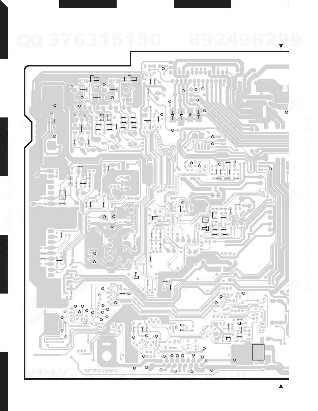
PC BOARD (FOIL SIDE VIEW)
Q
MAIN UNIT
TEL
Q
C222
C225
C226
C228
R223
7
3
TP69
D221
L222
TP68
Q5
C224
13942296513
R221
Q222
R240
C866
EB
L224
EB
TP11
SCL
R222
TP70
R231
L223
TP42
TP12
SDA
6
FL
C334
R334
TP78
R232
TP32
TP74
R331
C331
C235
R374
C375
TP38
R867
R271
TP77
TP76
R332
Q221
C233
TP39
3
R333
C333
DSG
C241
R237
TP35
TP34
D272
R272
R234
R233
TP36
TP37
TP33
FR
D271
C271
R273
R275
C240
MDR
MDL
TP26
TP28
1
TP73
TP71
C272
R274
R235
TAR
TP18
TP27
TP30
5
R868
R281
TP75
D273
C232
TAL
TP31
TP29
R276
TAG
TP10
1
RRRL
C270
R282
R283
C281
R285
C237
C238
R312
R32
R31
ROMCL WR
5
MAIN UNIT
C624 C625
D282
R284
TP72
C282
R286
D277
TP21
R22
TP113
R301
R48
Q601
R58
TP106
TP112
JC6
JC5
R16
R49
0
R631
C621
R628
R626
EB
Q
C118
D103
R304
R307
R36
R35
TP1
R624
R627
Q
R303
R306
R57
TP103
TP110
TP7
R302
R305
TP111
AC-GND
C8
R17
TP5
TP2
C119
R105
R19
TP109
TP108
TH601
D624
3
R106
C3
D2
4
2
9
8
TP4
TP6
TP88
TP86
TP87
D621
D622
D623
CDR
CDL
TP20
C294
TP22
R299 TP54
TP3
Q101
7
TP107
6
EB
TP105
3
TP101
TP102
1
Q102
C2
TP99
5
EB
D102
C291
R110
1
Q103
R109
C113
TP104
TP98
TP100
R298
L101
EB
EB
TP16
TP15
R297
5
Q104
TP17
R291
R135
0
R133
R134
R132
C114
L2
R38
C10
LED11
R293
R292
C292
C159
C13
43
12
TP66
TP9
R294
C160
R46
IC2
R295
C149
8
C150
Q1
R39
R40
9
R296
C293
9
C147
C152
TP19
D1
EB
2
R50
8
4
Q867
2
C12
9
8
BE
9
2
9
9
C11
TP95
TEL 13942296513 QQ 376315150 892498299
9
w
w
7
w
12
.
xia
o
y
u
1
6
3
.
c
o
m
 Loading...