

Page 1

Technical Reference
Model 5312B
Technical Reference
64970 Rev. F / 7-98
Page 2

WARRANTY
Hardware
Keithley Instruments, Inc. warrants that, for a period of one (1) year from the date of shipment (3 years for Models 2000, 2001, 2002, and 2010), the Keithley
Hardware product will be free from defects in materials or workmanship. This warranty will be honored provided the defect has not been caused by use of the
Keithley Hardware not in accordance with the instructions for the product. This warranty shall be null and void upon: (1) any modification of Keithley Hardware that is made by other than Keithley and not approved in writing by Keithley or (2) operation of the Keithley Hardware outside of the environmental specifications therefore.
Upon receiving notification of a defect in the Keithley Hardware during the warranty period, Keithley will, at its option, either repair or replace such Keithley
Hardware. During the first ninety days of the warranty period, Keithley will, at its option, supply the necessary on site labor to return the product to the condition prior to the notification of a defect. Failure to notify Keithley of a defect during the warranty shall relieve Keithley of its obligations and liabilities under
this warranty.
Other Hardware
The portion of the product that is not manufactured by Keithley (Other Hardware) shall not be covered by this w arranty, and Keithley shall hav e no duty of obligation to enforce any manufacturers' warranties on behalf of the customer. On those other manufacturers’ products that Keithley purchases for resale, Keithley
shall have no duty of obligation to enforce any manufacturers’ warranties on behalf of the customer.
Software
Keithley warrants that for a period of one (1) year from date of shipment, the Keithle y produced portion of the software or firmw are (Keithley Software) will conform in all material respects with the published specifications provided such Keithley Software is used on the product for which it is intended and otherwise in
accordance with the instructions therefore. Keithley does not warrant that operation of the Keithley Softw are will be uninterrupted or error-free and/or that the
Keithley Software will be adequate for the customer's intended application and/or use. This warranty shall be null and v oid upon an y modification of the K eithle y
Software that is made by other than Keithley and not approved in writing by Keithley.
If Keithley receiv es notification of a K eithle y Software nonconformity that is co v ered by this warranty during the w arranty period, K eithle y will review the conditions described in such notice. Such notice must state the published specification(s) to which the Keithley Software fails to conform and the manner in which
the Keithley Software fails to conform to such published specification(s) with sufficient specificity to permit K eithle y to correct such nonconformity. If Keithley
determines that the Keithley Software does not conform with the published specifications, Keithley will, at its option, provide either the programming services
necessary to correct such nonconformity or develop a program change to bypass such nonconformity in the Keithley Software. Failure to notify Keithley of a
nonconformity during the warranty shall relieve Keithley of its obligations and liabilities under this warranty.
Other Software
OEM software that is not produced by Keithley (Other Software) shall not be covered by this w arranty, and Keithley shall hav e no duty or obligation to enforce
any OEM's warranties on behalf of the customer.
Other Items
Keithley warrants the following items for 90 days from the date of shipment: probes, cables, rechar geable batteries, diskettes, and documentation.
Items not Covered under Warranty
This warranty does not apply to fuses, non-rechargeable batteries, damage from battery leakage, or problems arising from normal wear or failure to follow
instructions.
Limitation of Warranty
This warranty does not apply to defects resulting from product modification made by Purchaser without Keithley's express written consent, or by misuse of any
product or part.
Disclaimer of Warranties
EXCEPT FOR THE EXPRESS WARRANTIES ABOVE KEITHLEY DISCLAIMS ALL OTHER WARRANTIES, EXPRESS OR IMPLIED, INCLUDING
WITHOUT LIMIT ATION, ALL IMPLIED WARRANTIES OF MERCHANTABILITY AND FITNESS FOR A P ARTICULAR PURPOSE. KEITHLEY DISCLAIMS ALL WARRANTIES WITH RESPECT TO THE OTHER HARDWARE AND OTHER SOFTWARE.
Limitation of Liability
KEITHLEY INSTRUMENTS SHALL IN NO EVENT, REGARDLESS OF CAUSE, ASSUME RESPONSIBILITY FOR OR BE LIABLE FOR: (1) ECONOMICAL, INCIDENTAL, CONSEQUENTIAL, INDIRECT, SPECIAL, PUNITIVE OR EXEMPLARY DAMAGES, WHETHER CLAIMED UNDER
CONTRACT, TORT OR ANY OTHER LEGAL THEORY, (2) LOSS OF OR DAMAGE TO THE CUSTOMER'S DATA OR PROGRAMMING, OR (3) PENAL TIES OR PENALTY CLAUSES OF ANY DESCRIPTION OR INDEMNIFICATION OF THE CUST OMER OR O THERS FOR COSTS, DAMAGES, OR
EXPENSES RELATED TO THE GOODS OR SERVICES PROVIDED UNDER THIS WARRANTY.
Keithley Instruments, Inc. • 28775 Aurora Road • Cleveland, OH 44139 • 440-248-0400 • Fax: 440-248-6168 • http://www.keithley.com
CHINA: Keithley Instruments China • Yuan Chen Xin Building, Room 705 • 12 Yumin Road, Dewai, Madian • Beijing 100029 • 8610-62022886 • Fax: 8610-62022892
FRANCE: Keithley Instruments SARL • BP 60 • 3 Allée des Garays • 91122 Palaiseau Cédex • 33-1-60-11-51-55 • Fax: 33-1-60-11-77-26
GERMANY: Keithley Instruments GmbH • Landsberger Strasse 65 • D-82110 Germering, Munich • 49-89-8493070 • Fax: 49-89-84930759
GREAT BRITAIN: Keithley Instruments, Ltd. • The Minster • 58 Portman Road • Reading, Berkshire RG30 1EA • 44-1189-596469 • Fax: 44-1189-575666
ITALY: Keithley Instruments SRL • Viale S. Gimignano 38 • 20146 Milano • 39-2-48303008 • Fax: 39-2-48302274
NETHERLANDS: Keithley Instruments BV • Avelingen West 49 • 4202 MS Gorinchem • 31-(0)183-635333 • Fax: 31-(0)183-630821
SWITZERLAND: Keithley Instruments SA • Kriesbachstrasse 4 • 8600 Dübendorf • 41-1-8219444 • Fax: 41-1-8203081
TAIWAN: Keithley Instruments Taiwan • 1FL., 85 Po Ai Street • Hsinchu, Taiwan • 886-3-572-9077 • Fax: 886-3-572-9031
Page 3

Model 5312B
Technical Reference
©1995, Keithley Instruments, Inc.
All rights reserved.
Cleveland, Ohio, U.S.A.
Second Printing, July 1998
Document Number: 64970 Rev. F
Page 4

Manual Print History
The print history shown below lists the printing dates of all Revisions and Addenda created for this manual. The Revision
Level letter increases alphabetically as the manual undergoes subsequent updates. Addenda, which are released between Revisions, contain important change information that the user should incorporate immediately into the manual. Addenda are numbered sequentially. When a new Revision is created, all Addenda associated with the previous Revision of the manual are
incorporated into the new Revision of the manual. Each new Revision includes a revised copy of this print history page.
Revision E (Document Number 64970) ............................................................................................. January 1996
Revision F (Document Number 64970) ................................................................................................... July 1998
All Keithley product names are trademarks or registered trademarks of Keithley Instruments, Inc.
Other brand and product names are trademarks or registered trademarks of their respective holders.
Page 5

Safety Precautions
The following safety precautions should be observed before using
this product and any associated instrumentation. Although some instruments and accessories would normally be used with non-hazardous voltages, there are situations where hazardous conditions
may be present.
This product is intended for use by qualified personnel who recognize shock hazards and are familiar with the safety precautions required to avoid possible injury. Read the operating information
carefully before using the product.
The types of product users are:
Responsible body is the individual or group responsible for the use
and maintenance of equipment, and for ensuring that operators are
adequately trained.
Operators use the product for its intended function. They must be
trained in electrical safety procedures and proper use of the instrument. They must be protected from electric shock and contact with
hazardous live circuits.
Maintenance personnel perform routine procedures on the product
to keep it operating, for example, setting the line voltage or replacing consumable materials. Maintenance procedures are described in
the manual. The procedures explicitly state if the operator may perform them. Otherwise, they should be performed only by service
personnel.
Service personnel are trained to work on live circuits, and perform
safe installations and repairs of products. Only properly trained service personnel may perform installation and service procedures.
Exercise extreme caution when a shock hazard is present. Lethal
voltage may be present on cable connector jacks or test fixtures. The
American National Standards Institute (ANSI) states that a shock
hazard exists when voltage levels greater than 30V RMS, 42.4V
peak, or 60VDC are present. A good safety practice is to expect
that hazardous voltage is present in any unknown circuit bef ore
measuring.
Users of this product must be protected from electric shock at all
times. The responsible body must ensure that users are prevented
access and/or insulated from every connection point. In some cases,
connections must be exposed to potential human contact. Product
users in these circumstances must be trained to protect themselves
from the risk of electric shock. If the circuit is capable of operating
at or above 1000 volts, no conductive part of the circuit may be
exposed.
As described in the International Electrotechnical Commission
(IEC) Standard IEC 664, digital multimeter measuring circuits
(e.g., Keithley Models 175A, 199, 2000, 2001, 2002, and 2010) are
Installation Category II. All other instruments’ signal terminals are
Installation Category I and must not be connected to mains.
Do not connect switching cards directly to unlimited power circuits.
They are intended to be used with impedance limited sources.
NEVER connect switching cards directly to AC mains. When connecting sources to switching cards, install protective devices to limit fault current and voltage to the card.
Before operating an instrument, make sure the line cord is connected to a properly grounded power receptacle. Inspect the connecting
cables, test leads, and jumpers for possible wear, cracks, or breaks
before each use.
For maximum safety, do not touch the product, test cables, or any
other instruments while power is applied to the circuit under test.
ALWAYS remove power from the entire test system and discharge
any capacitors before: connecting or disconnecting cables or jumpers, installing or removing switching cards, or making internal
changes, such as installing or removing jumpers.
Do not touch any object that could provide a current path to the
common side of the circuit under test or power line (earth) ground.
Always make measurements with dry hands while standing on a
dry, insulated surface capable of withstanding the voltage being
measured.
Page 6

Do not exceed the maximum signal levels of the instruments and accessories, as defined in the specifications and operating information, and as shown on the instrument or test fixture panels, or
switching card.
When fuses are used in a product, replace with same type and rating
for continued protection against fire hazard.
Chassis connections must only be used as shield connections for
measuring circuits, NOT as safety earth ground connections.
If you are using a test fixture, keep the lid closed while power is applied to the device under test. Safe operation requires the use of a
lid interlock.
If a screw is present, connect it to safety earth ground using the
wire recommended in the user documentation.
!
The symbol on an instrument indicates that the user should refer to the operating instructions located in the manual.
The symbol on an instrument shows that it can source or measure 1000 volts or more, including the combined effect of normal
and common mode voltages. Use standard safety precautions to
avoid personal contact with these voltages.
The WARNING heading in a manual explains dangers that might
result in personal injury or death. Alw ays read the associated infor mation very carefully before performing the indicated procedure.
Instrumentation and accessories shall not be connected to humans.
Before performing any maintenance, disconnect the line cord and
all test cables.
To maintain protection from electric shock and fire, replacement
components in mains circuits, including the power transformer, test
leads, and input jacks, must be purchased from Keithley Instruments. Standard fuses, with applicable national safety approvals,
may be used if the rating and type are the same. Other components
that are not safety related may be purchased from other suppliers as
long as they are equivalent to the original component. (Note that selected parts should be purchased only through Keithley Instruments
to maintain accuracy and functionality of the product.) If you are
unsure about the applicability of a replacement component, call
technical support for information.
To clean the instrument, use a damp cloth or mild, water based
cleaner. Clean the exterior of the instrument only. Do not apply
cleaner directly to the instrument or allow liquids to enter or spill
on the instrument.
The CAUTION heading in a manual explains hazards that could
damage the instrument. Such damage may invalidate the warranty.
Page 7

About this manual
Quality control
Keithley Instruments manufactures quality and versatile products, and we want our documentation to reflect that same quality. We take great pains to publish manuals that are informative and
well organized. We also strive to make our documentation easy to understand for the novice as
well as the expert.
If you have comments or suggestions about how to mak e this (or other) manuals easier to understand, or if you find an error or an omission, please fill out and mail the reader response card at
the end of this manual (postage is prepaid).
Conventions
Procedural
Keithley Instruments uses various conventions throughout this manual. You should become
familiar with these conventions as they are used to draw attention to items of importance and
items that will generally assist you in understanding a particular area.
WARNING
CAUTION
NOTE
When referring to pin numbering, pin 1 is always associated with a square solder pad on the
actual component footprint.
A warning is used to indicate that an action must be done with great
care. Otherwise, personal injury may result.
A caution is used to indicate that an action may cause minor equipment damage or the loss of data if not performed carefully.
A note is used to indicate important information needed to perform an
action or information that is nice-to-know.
Notational
A forward slash (/) preceding a signal name denotes an active LOW signal. This is a standard
Intel convention.
Caret brackets (<>) denote keystrokes. For instance <Enter> represents carriage-return-withline-feed keystroke, and <Esc> represents an escape keystroke.
Driver routine declarations are shown for C and BASIC (where applicable).
Hungarian notation is used for software parameters. In other words, the parameter type is
denoted by a one or two letter lower case prefix:
c character, signed or unsigned
s short integer, signed
w short integer, unsigned
l long integer, signed
dw long integer, unsigned
For example, wBoardAddr would be an unsigned short integer parameter.
Page 8

An additional p prefix before the type prefix indicates that the parameter is being passed by reference instead of by value. (A pointer to the variable is being passed instead of the variable
itself).
For example, pwErr would be an unsigned short integer parameter passed by reference.
This notation is also used in BASIC although no distinction between signed and unsigned vari-
ables exists.
In BASIC, all parameters also have a type suffix:
$ character, signed or unsigned
% integer, signed or unsigned
& long integer, signed or unsigned
Routine names are printed in bold font when they appear outside of function declarations, e.g.,
ReadStatus.
Parameter names are printed in italics when they appear outside of function declarations, e.g.
sControls.
Constants are defined with all caps, e.g., ALL_AXES. Underscores {_} must be replaced by
periods {.} for use with BASIC.
Combinational logic and hexadecimal notation is in C convention in many cases. For example,
the hexadecimal number 7Ch is shown as 0x7C.
C relational operators for OR and AND functions — “| |” and “&&” — are used to minimize the
confusion associated with grammar.
Page 9

Table of Contents
1 Introduction and Installation
Description ......................................................................................................................................................... 1-2
Technical Specifications .................................................................................................................................... 1-3
Setting the jumpers ............................................................................................................................................. 1-3
Base adddressing ........................................................................................................................................ 1-4
Indirect addressing ..................................................................................................................................... 1-5
Termination resistors .................................................................................................................................. 1-6
Selecting an index option ........................................................................................................................... 1-8
Selecting the card configuration ................................................................................................................. 1-9
Interrupt selection .................................................................................................................................... 1-10
Wait states ................................................................................................................................................ 1-11
Installation ........................................................................................................................................................ 1-11
Power considerations ............................................................................................................................... 1-12
Connector pinouts .................................................................................................................................... 1-13
2 Operation and Programming
Theory of operation ............................................................................................................................................ 2-2
Programming ...................................................................................................................................................... 2-2
Writing the Preset Register (PR) ................................................................................................................ 2-2
Reading the Output Latch register (OL) .................................................................................................... 2-3
Writing the Command Register (CR) ........................................................................................................ 2-3
Master Control Register (MCR) ................................................................................................................ 2-3
Input Control Register (ICR) ..................................................................................................................... 2-4
Output/Counter Control Register (OCCR) ................................................................................................. 2-4
Quadrature Register (QR) .......................................................................................................................... 2-5
Output Status Register (OSR) .................................................................................................................... 2-6
Typical programming examples ................................................................................................................. 2-6
Selecting a sample clock frequency ........................................................................................................... 2-8
i
Page 10

3 Interrupt Control
Description of interrupt control ......................................................................................................................... 3-2
Interrupt Request Rgtr (IRR), In Service Rgtr (ISR) ................................................................................. 3-2
Priority Resolver (PR) ................................................................................................................................ 3-3
Interrupt Mask Register (IMR) ................................................................................................................... 3-3
Interrupt output (INT) ................................................................................................................................. 3-3
PIC operation ...................................................................................................................................................... 3-3
Interrupt sequence, 80x86/80x88 mode ..................................................................................................... 3-3
End-of-interrupt command ......................................................................................................................... 3-4
Completing an interrupt .............................................................................................................................. 3-4
Operating modes ................................................................................................................................................. 3-4
Fully nested mode ....................................................................................................................................... 3-4
Special mask mode ..................................................................................................................................... 3-5
Specific rotation (specific priority) ............................................................................................................ 3-5
Automatic rotation (equal priority) ............................................................................................................ 3-5
Non-vectored mode (poll command) .......................................................................................................... 3-5
PIC programming ............................................................................................................................................... 3-5
Initialization Command Words (ICW) ....................................................................................................... 3-5
ICW1 format and description ..................................................................................................................... 3-6
ICW4 format and description ..................................................................................................................... 3-7
Operation Command Words (OCW) .......................................................................................................... 3-7
OCW1 format and description .................................................................................................................... 3-8
OCW2 format and description .................................................................................................................... 3-9
OCW2 commands ...................................................................................................................................... 3-9
OCW3 format and description .................................................................................................................... 3-9
A PC I/O and Interrupt Mapping
PC I/O map ........................................................................................................................................................ A-2
B T ech Bulletins and Application Notes
Timer application in velocity mode ................................................................................................................... B-2
Setting up axis 3 as an interval timer ................................................................................................................. B-2
C Circuit Diagrams
ii
Page 11

List of Illustrations
1 Introduction and Installation
Figure 1-1 Functional block diagram for the 5312 ...................................................................................................... 1-2
Figure 1-2 Jumper locations for the 5312 .................................................................................................................... 1-4
Figure 1-3 Encoder termination resistor locations ....................................................................................................... 1-7
Figure 1-4 LED locations on the card edge ................................................................................................................. 1-7
Figure 1-5 Connector locations on the board ............................................................................................................. 1-12
2 Operation and Programming
Figure 2-1 Example of a 4-stage signal conditioning filter ......................................................................................... 2-8
3 Interrupt Control
Figure 3-1 PIC block level diagram ............................................................................................................................. 3-2
Figure 3-2 PIC initialization sequence ......................................................................................................................... 3-5
Figure 3-3 PIC ICW format ......................................................................................................................................... 3-6
Figure 3-4 PIC OCW format ....................................................................................................................................... 3-8
iii
Page 12

List of Tables
1 Introduction and Installation
Table 1-1 W19, base address select (upper nibble) .................................................................................................... 1-4
Table 1-2 5312 I/O map ............................................................................................................................................. 1-5
Table 1-3 Termination resistors in differential mode.................................................................................................. 1-6
Table 1-4 Terminal resistors in single-ended mode ................................................................................................... 1-6
Table 1-5 Index option selections ............................................................................................................................... 1-8
Table 1-6 Jumper selection for differential/single-ended operation ........................................................................... 1-9
Table 1-7 Sample clock frequency jumper settings .................................................................................................... 1-9
Table 1-8 Cascading the counters ............................................................................................................................. 1-10
Table 1-9 Jumpering for disabling/enabling borrow interrupts ................................................................................ 1-10
Table 1-10 Selecting an interrupt ............................................................................................................................... 1-10
Table 1-11 Generating wait states .............................................................................................................................. 1-11
Table 1-12 Connector J1-J4 pin assignments ............................................................................................................. 1-13
Table 1-13 Default jumper settings for all board versions ......................................................................................... 1-14
2 Operation and Programming
Table 2-1 Register select ............................................................................................................................................ 2-3
Table 2-2 Output/counter control modes .................................................................................................................... 2-5
Table 2-3 Quadrature register modes ......................................................................................................................... 2-5
3 Interrupt Control
Table 3-1 Interrupt code ............................................................................................................................................. 3-4
A PC I/O Map
Table A-1 PC I/O map ................................................................................................................................................ A-2
Table A-2 PC interrupt map ....................................................................................................................................... A-3
v
Page 13

1
Introduction and Installation
Page 14

1-2 Introduction and Installation Model 5312B Technical Reference
Description
NOTE
The 5312 Quadrature Encoder card is PC bus compatible. It provides inputs and decoding for
up to four incremental quadrature encoders depending on the model purchased. You may also
use the card as a high-speed pulse counter (up/down and pulse/direction) for general counting
applications. Figure 1-1 shows a functional block diagram.
Figure 1-1
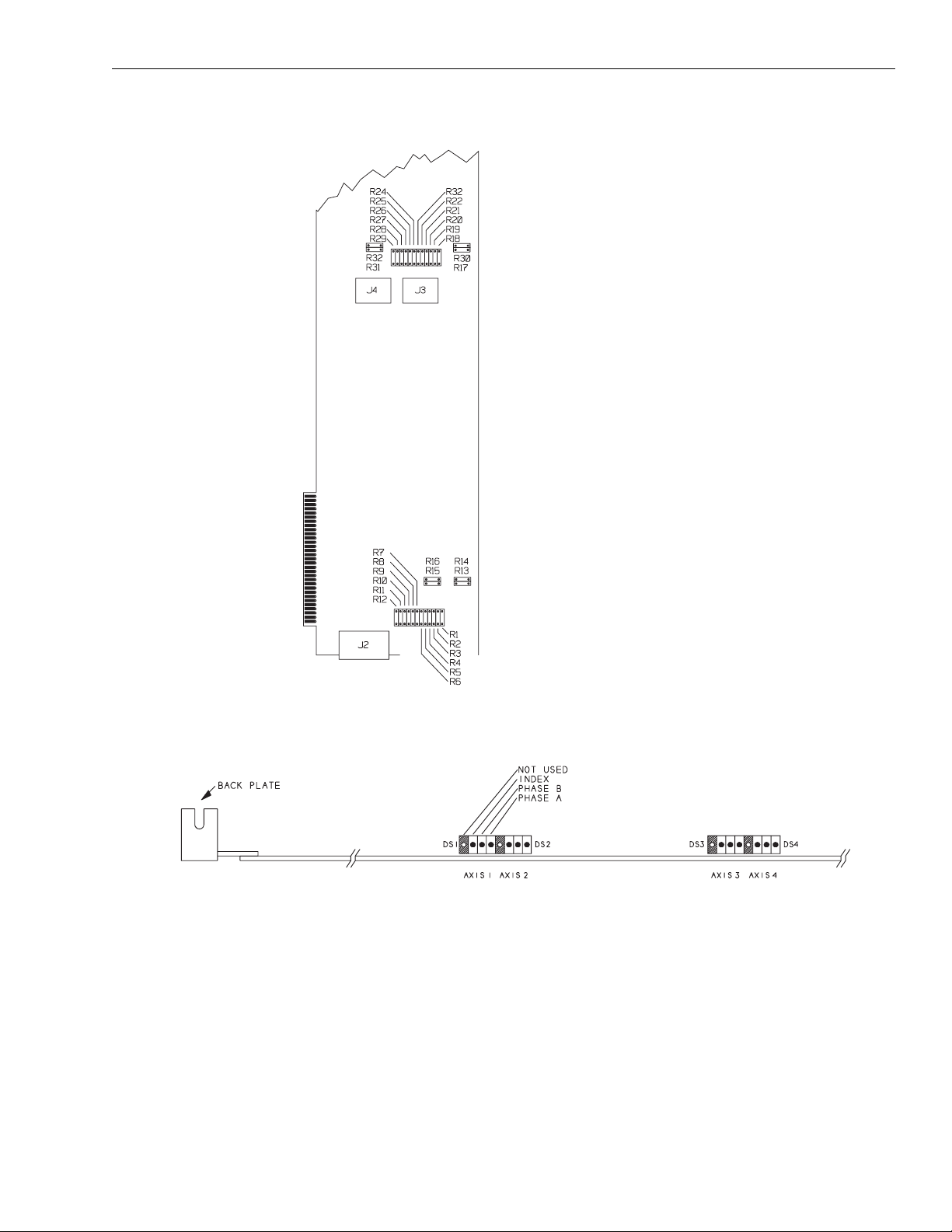
Functional block diagram for the 5312
This manual is model dependent. For models not using all encoder
ports, disregard the appropriate upper axis.
For each encoder circuit, Phase A (Phase 0), Phase B (Phase 90), and Inde x pulse inputs are provided. Jumper options on board allow you to configure the inputs as single-ended TTL or dif fer ential (the recommended connection method). Individual connectors for each encoder provide
power (+5V) and ground for the encoder if needed.
You can also use the 5312 as pulse counter for up to 4 independent events, or you can cascade
the counters to provide high speed pulse counting over an extended count range.
Inputs are conditioned by a 4-stage digital filter. The filter clock is one of five jumper -selectable
sampling frequencies ranging up to 10 MHz. Selecting the lowest frequency compatible with
the highest expected input rate will maximize noise immunity. The maximum input rate per
phase in quadrature decode mode is approximately 333 kHz. The maximum input rate in count
mode is approximately 1.25 MHz. Sample clock frequency selection is described in detail in
Section 2.
The conditioned inputs are applied to a 24-bit counter provided for each encoder. You can use
the counters for quadrature decoding, pulse and direction input counting, or as a pulse input up/
down counter. Count output is available for the PC bus in binary or binary coded decimal
(BCD) form. The count value may be latched on command, latched on an index pulse, or
latched with a new count value when an index pulse occurs.
Page 15

Model 5312B Technical Reference Introduction and Installation 1-3
The 5312 is capable of generating interrupts. Maskable interrupts may come from a valid index
pulse, counter overflow/underflow, or on count value match with a preset compare value.
T echnical specifications
Voltage Requirements: 4-axis: 1.5A (typical), 2.0A (maximum)
3-axis: 1.25A (typical), 1.75A (maximum)
2-axis: 1.0A (typical), 1.5A (maximum)
1-axis: 0.9A (typical), 1.25A (maximum)
Compatibility : PC/XT/AT
Single-ended or Differential
Incremental Encoders
TTL or CMOS Signal Sources
Operating Range: 0 to 70 degrees Celsius
Mating Connectors:
Card Dimensions: 13.3 x 4.2 x 0.5 inches
Setting the jumpers
CAUTION Always remove power from the PC and any external system
Jumper options on the 5312 offer a great deal of flexibility in system operation. These options
are grouped into 4 areas according to functions — encoder inputs, card functions, interrupt
action, and card addressing.
All cards are shipped with most jumpers installed for a given configuration. All factory default
jumpers are indicated throughout this manual in the appropriate tables with a † symbol. However, due to possible rough handling during shipment, there is no assurance that all jumpers will
be in the indicated position.
NOTE
9-pin Dsub:
devices before removing any connection on the 5312. Failure to do
so may result in permanent damage to the card and will void any
warranty.
Default jumper settings shown are those for the 4-axis version of the
M5312. For default settings on other versions, see Table 1-13 at the
end of Section 1.
Ansley 609-9p
Amphenol
841-17-DEFR-B09P
Check and properly configure all boards before installing.
Jumper locations are shown in Figure 1-2. We strongly recommend, however, that once you
determine the proper jumper settings, replace all jumpers with more reliable wire-wrapped connections. This is particularly important when exposing the card to an industrial environment
where vibration, dust, oil, or other contaminants may be present.
Page 16

1-4 Introduction and Installation Model 5312B Technical Reference
Base addressing
Jumper W19 determines the upper nibble (4 bits) of the card base address according to Table 1-1.
Table 1-1
W19, base address select (upper nibble)
W19 Base Address
(1-2)†
(2-3)
† Default jumper setting
Set hex switches SW1 and SW2 to determine the lower 8 bits of the address. Switch SW2 represents the most significant nibble (MSN), and SW1 represents the least significant nibble (LSN).
Since the 5312 occupies two adjacent I/O ports, only the even settings of the LSN switch are
used.
Figure 1-2
Jumper locations for the 5312
2 xx h
3 xx h
1
W5
1
W5
1
W4
W4
W4
W4
W4
W3
W3
1
W3
1
W3
1
W2
1
W2
1
W2
W2
W2
1
2
W1
9
10
W
W
W2
W3
W3
W3
W3
W2
W2
1
W2
1
W1
1
1
1
SW
SW
W
W
W
1
W1
W1
W
1
9
W2
11111
WW4W1W4W
WW4W
WW3W
1
W4
W4
W3
2
10
W
W
Page 17

Model 5312B Technical Reference Introduction and Installation 1-5
Indirect addressing
To conserve I/O space on the PC bus, the 5312 is indirectly addressed (see Table 1-2). This
allows the card to occupy only two direct I/O ports by using one for indirect addressing (e v en or
lower) and the other for data (the odd or greater of the two ports). The sequence for writing to
any indirect port is to first write the indirect port address to the address port. The desired data
can then be written to the data port. This indirect port will remain addressed until the indirect
address port is again written. For example, to write the initialization bytes MCR, ICR, OCCR,
and QR to the command port of axis 1 assuming the card is strapped to 300h as the base address:
1. Write the indirect address for the axis A command port (01h) to the indirect address port
(300h).
2. Write the first byte (Master Control Register) to the data port (301h).
3. Write the second byte (Input Control Register) to the data port (301h).
4. Write the third byte (Output/Counter Control Register) to the data port (301h).
5. Write the last byte (Quadrature Encoder) to the data port (301h).
NOTE
The C function libraries on the software diskette make this sequence
transparent to the user.
Table 1-2
5312 I/O map
Axis Address When Written When Read
1 00 Write to preset register (PR) and
increment register address
counter.
01 Write to command register. Read OSR (output status
2 02 Write to PR and increment
register address counter.
03 Write to command register. Read OSR.
3 04 Write to PR and increment
register address counter.
05 Write to command register. Read OSR.
4 06 Write to PR and increment
register address counter.
07 Write to command register. Read OSR.
Global 08 Global write to all four PRs. Invalid
09 Global write to all four command
registers.
PIC 0A Low Port Low Port
0B High Port High Port
Read OL (output latch) and
increment register address
counter.
register).
Read OL and increment
register address counter.
Read OL and increment
register address counter.
Read OL and increment
register address counter.
Invalid
Page 18

1-6 Introduction and Installation Model 5312B Technical Reference
T ermination resistors
If differential input is used, give consideration to terminating the cable lines connecting the signal to the card. Cable length and signal frequency determine how critical the termination factor
is. Since the needed termination resistor value is determined by cable type, sockets are provided
for easy insertion and removal of termination resistors. Unless otherwise specified by the
encoder manufacturer, one-quarter watt carbon film resistors of a standard EIA value closest to
one half the characteristic impedance of the cable are adequate (see cable manufacturers specification for values). Termination resistors apply a load to the signal source, so make sure that the
source can supply enough drive capability to compensate for this condition.
Figure 1-3 shows the termination resistor locations for both single-ended and differential. Table
1-3 shows the termination resistor assignments for each signal in differential mode. The inputs
should be terminated in the characteristic impedance of the input line.
Table 1-3
Termination resistors in differential mode
Signal Axis 1 Axis 2 Axis 3 Axis 4
Phase A
Phase B
Index
R1, R2
R3, R4
R5, R6
R7, R8
R9, R10
R11, R12
R18, R19
R20, R21
R22, R23
R24, R25
R26, R27
R28, R29
When single-ended encoder inputs are used, the logic level of the input signal is determined by
comparison with a reference voltage on the card. This reference is set by a pair of resistors
selected and inserted by the user, and they form a voltage divider network that establishes the
center point for the input Hysteresis band.
Resistor assignments in a single-ended mode are shown in Table 1-4.
Table 1-4
Termination resistors in single-ended mode
Typical Value Axis 1 Axis 2 Axis 3 Axis 4
220 Ohms
150 Ohms
The 5312 features encoder input indicators that are useful when determining proper encoder
operation and connection. Only three of the four LEDs in each package are used. Figure 1-4
shows the location of LEDs on the outboard edge of the card as you view do wn from the top. An
LED is on when its corresponding input signal is LOW.
R14
R14
R15
R16
R17
R30
R31
R32
Page 19
Model 5312B Technical Reference Introduction and Installation 1-7
Figure 1-3
Encoder termination resistor locations
Figure 1-4
LED
locations on the card edge
Page 20

•
•
•
•
1-8 Introduction and Installation Model 5312B Technical Reference
Selecting an index option
The following are the available jumper options that direct the function of the encoder index
pulse. The first two options work in conjunction with bits D4 and D5 respectively of the Input
Control Register (ICR). Table 1-5 shows the jumper configuration for selecting an index option.
Index Action to /ABGT (ABGaTe) or /RCTR (Reset CounTeR):
ICRB4 = 0:A valid index level will reset the counter.
ICRB4 = 1:A valid index level will gate phase A and B inputs to the counter.
Index Action to /LCTR (Load CounTer) or /LLTC (Load output LaTCh).
ICRB5 = 0:A valid index level will load the contents of the preset register into the counter.
ICRB5 = 1:A valid index level will load the contents of the counter into the Output Latch.
Active Low Index Polarity.
Select this option if the encoder provides an active LOW index pulse.
Active High Index Polarity.
Select this option if the encoder provides an active HIGH index pulse.
Correct strapping for each axis is detailed in Table 1-6 below. The following tables also provide
the necessary jumpering information for operating the encoder.
If the index is not used, remove jumpers W17, W22, and W29. Failure to do so will result in
incorrect encoder operation. If index is used, we recommend that you check for correct encoder
operation with the jumpers removed, then with the jumpers installed.
Table 1-5
Index option selections
Operation Axis 1 Axis 2
Index Action
W24(2-3) W17(2-3) W22(2-3) W29(2-3)
Axis 3
Axis 4
/ABGT-/RCTR† (AB GateReset Counter)
Index Action
W24(1-2)† W17(1-2)† W22(1-2)† W29(1-2)†
/LCTR-/LL TC†
(Load Counter-Load Latch)
Active LOW Index Polarity W13(2-3)† W16(2-3)‡ W51(2-3)† W50(2-3)†
Active HIGH Index Polarity W13(1-2) W16(1-2)†‡ W51(1-2) W50(1-2)
† Default jumper setting
‡
For axis 2, strap (1-2) for active LOW, (2-3) for active HIGH
Note: A forward slash preceding a signal name denotes an active LOW signal.
Page 21

Model 5312B Technical Reference Introduction and Installation 1-9
Table 1-6
Jumper selection for differential/single-ended operation
Axis Operating Mode Jumpers Strapping
1 Differential
Single-Ended
2 Differential
Single-Ended
3 Differential
Single-Ended
4 Differential
Single-Ended
†
Default jumper setting
W1, W3, W5
W2, W4, W6
W1, W3, W5
W2, W4, W6
W7, W9, W11
W8, W10, W12
W7, W9, W11
W8, W10, W12
W38, W40, W42
W39, W41, W43
W38, W40, W42
W39, W41, W43
W44, W46, W48
W45, W47, W49
W44, W46, W48
W45, W47, W49
none
(1-2)
(1-2)†
(2-3)†
none
(1-2)
(1-2)†
(2-3)†
none
(1-2)
(1-2)†
(2-3)†
none
(1-2)
(1-2)†
(2-3)†
Selecting the card configuration
The following tables provide the necessary jumpering information for selecting card function.
Sample clock frequency jumpering
Jumper W23 (Table 1-7) is used to select the sample clock frequency used by the digital filters.
For more information, see Section 2.
Table 1-7
Sample clock frequency jumper settings
Sample Clock Frequency (MHz) W23
0.625
1.250
2.500
5.000
10.00
†Default jumper setting
(9-10)†
(7-8)
(5-6)
(3-4)
(1-2)
Page 22

1-10 Introduction and Installation Model 5312B Technical Reference
Counter cascading
If you need to extend the counting range of the 5312, you can cascade the counters according to
Table 1-8.
Table 1-8
Cascading the counters
Operation Jumper Strapping
Cascade Axis 1 to Axis 2
No Cascading Axis 1 to Axis 2
Cascade Axis 2 to Axis 3
No Cascading Axis 2 to Axis 3
Cascade Axis 3 to Axis 4
No Cascading Axis 3 to Axis 4
† Default jumper setting
W28, W25
W28, W25
W27, W31
W27, W31
W33, W37
W33, W37
(2-3)†
(1-2)†
(2-3)†
(1-2)†
(2-3)†
(1-2)†
Interrupt selection
Enabling and disabling PIC interrupts
T able 1-9 provides the necessary information for enabling and disabling Programmable Interrupt
Control (PIC) interrupts. For further information on interrupt selection, refer to Section 2.
Table 1-9
Jumpering for disabling/enabling borrow interrupts
Operation Axis 1 Axis 2 Axis 3 Axis 4 Strapping
Disable‡
/BW† (borrow) output to the PIC
Enable
/BW† output to the PIC
† Default jumper setting
‡ Disable /BW to use comparator mode
Note: A forward slash (/) preceding a signal name denotes an active LOW signal.
PC bus interrupts
W18 selects the PC bus interrupt request line used for interrupt operation as shown in Table 1-10.
Table 1-10
Selecting an interrupt
W26
W26
W32
W32
W35
W35
W36
W36
(1-2)
(2-3)†
Interrupt
W18
(1-2)
(3-4)†
(5-6)
(7-8)
(9-10)
(11-12)
† Default jumper setting
‡ Unused on XT only, not available on AT
Request Line Hardware Interrupt
IRQ2
IRQ3
IRQ4
IRQ5
IRQ6
IRQ7
Unused‡
Unused
Serial Port
Unused
Diskette Port
Parallel Printer Port
Interrupt
Number
0Ah
0Bh
0Ch
0Dh
0Eh
0Fh
Page 23

Model 5312B Technical Reference Introduction and Installation 1-11
W ait states
A wait state is a period of time requested by a peripheral device to pause the host computer during a read or write operation. A de vice pauses the host to ensure that v alid data are passed. Each
wait state is equal to 1 clock cycle. Without wait states on the host, faster PCs will terminate an
operation before the peripheral card can fully and reliably gate the data in from or out to the PC
bus. As shipped, the card is jumpered for 2 wait states, although some slower PCs may be able
to use the card with less than 2. Jumpers W34 and W30 determine the number of wait states as
shown in Table 1-11.
Table 1-11
Generating wait states
Wait State W34 W30
none
1
2
Invalid
† Default jumper setting
none
none
installed†
installed
none
installed
none†
installed
Installation
The 5312 is designed to operate in a PC backplane or on a motherboard. You may install the
board into any 8-bit slot in the PC according to the PC manufacturer's instructions. If you use
more than 2 of the 4 available axes, an additional expansion slot is required. Connect ribbon
cables as required from J3 and J4 to the additional back plate.
Give consideration to power and ground connections to ensure reliable system operation.
Encoder connections are made to the card through up to 4 9-pin, Dsub connectors. Board connections are located according to Figure 1-5.
The pin assignments for these connectors are shown in section Connector pinouts.
Properly phase the encoder according to manufacturer's instructions.
Page 24

1-12 Introduction and Installation Model 5312B Technical Reference
Figure 1-5
Connector locations on the board
Power considerations
The Model 5312 requires +5V from the PC bus. The typical current load is 1A with a maximum
of 1.5A depending on the number of axes used. In addition, +5V is available at J1, J2, J3, and J4
for any external devices that need +5V. The total current load must be considered when determining how much power is required for the system.
Page 25

Model 5312B Technical Reference Introduction and Installation 1-13
Connector pinouts
Table 1-12 lists the pin assignments for J1 to J4 . The view shown of the connector is looking
into the board from the backpanel. Figure 1-5 shows the connector locations on the board. Ribbon cables connect axes 3 and 4 from the 10–pin unshrouded headers to chassis I/O slots on the
backpanel. The pinout on the backpanel connectors is the same as for axes 1 and 2.
Table 1-12
Connector J1-J4 pin assignments
Pin Single-Ended Differential
1
Ground
2
+5V
3
Ground
4
+5V
5
Ground
6
Phase A
7
Phase B
8
Ground
9
Index
† A forward slash (/) preceding a signal name denotes an
active LOW signal.
/Phase A†
+5V
/Phase B†
+5V
/Index†
Phase A
Phase B
Ground
Index
Page 26

1-14 Introduction and Installation Model 5312B Technical Reference
Table 1-13
Default jumper settings for all board versions
Jumper
W1
W2
W3
W4
W5
W6
W7
W8
W9
W10
W11
W12
W13
W16
W17
W18
W19
W22
W23
W24
W25
W26
W27
W28
W29
W30
W31
W32
W33
W34
W35
W36
W37
W38
W39
W40
W41
W42
W43
W44
W45
W46
W47
W48
W49
W50
W51
4-Axis
(1-2)
(2-3)
(1-2)
(2-3)
(1-2)
(2-3)
(1-2)
(2-3)
(1-2)
(2-3)
(1-2)
(2-3)
(2-3)
(1-2)
(1-2)
(3-4)
(1-2)
(1-2)
(9-10)
(1-2)
(1-2)
(2-3)
(1-2)
(1-2)
(1-2)
none
(1-2)
(2-3)
(1-2)
(1-2)
(2-3)
(2-3)
(1-2)
(1-2)
(2-3)
(1-2)
(2-3)
(1-2)
(2-3)
(1-2)
(2-3)
(1-2)
(2-3)
(1-2)
(2-3)
(2-3)
(2-3)
3-Axis
(1-2)
(2-3)
(1-2)
(2-3)
(1-2)
(2-3)
(1-2)
(2-3)
(1-2)
(2-3)
(1-2)
(2-3)
(2-3)
(1-2)
(1-2)
(3-4)
(1-2)
(1-2)
(9-10)
(1-2)
(1-2)
(2-3)
(1-2)
(1-2)
none
none
(1-2)
(2-3)
none
(1-2)
(2-3)
none
none
(1-2)
(2-3)
(1-2)
(2-3)
(1-2)
(2-3)
none
none
none
none
none
none
none
(2-3)
2-Axis
(1-2)
(2-3)
(1-2)
(2-3)
(1-2)
(2-3)
(1-2)
(2-3)
(1-2)
(2-3)
(1-2)
(2-3)
(2-3)
(1-2)
(1-2)
(3-4)
(1-2)
none
(9-10)
(1-2)
(1-2)
(2-3)
none
(1-2)
none
none
none
(2-3)
none
(1-2)
none
none
none
none
none
none
none
none
none
none
none
none
none
none
none
none
none
1-Axis
(1-2)
(2-3)
(1-2)
(2-3)
(1-2)
(2-3)
none
none
none
none
none
none
(2-3)
none
none
(3-4)
(1-2)
none
(9-10)
(1-2)
none
(2-3)
none
none
none
none
none
none
none
(1-2)
none
none
none
none
none
none
none
none
none
none
none
none
none
none
none
none
none
Page 27

2
Operation
and Programming
Page 28

•
•
•
•
2-2 Operation and Programming Model 5312B Technical Reference
•
•
•
Theory of operation
The Model 5312 can be configured for up to 4 independent 24-bit multimode counters depending on the model purchased. All models are PC/XT/AT compatible. For applications requiring
more than 24 bits of count range, the counters can be cascaded together to form various 24-bit
counter configurations. For example, you can cascade counters to obtain one 48-bit counter, a
24-bit counter and a 72-bit counter, or even one 96-bit counter.
Each counter is capable of numerous modes. Examples include:
A/B quadrature with a maximum input frequency of .333 MHz
Up/down count with a maximum input frequency of 1.25 MHz
Count/direction with a maximum input frequency of 1.25 MHz
Divide by n mode with a maximum input frequency of 1.25 MHz
All three inputs to each counter — Phase A, Phase B, and Index — can be connected singleended TTL or differential for greater noise immunity. The 5312 provides sockets in differential
mode to allow easy insertion of termination resistors. The input lines do not need to be terminated, but for best noise immunity terminate them at the characteristic impedance of the input
line. Each input is tied through a buffer to an LED which is turned on when the respective input
is LOW.
Programming
Writing the Preset Register (PR)
Each input is digitally filtered (see section Selecting a sample clock frequency) using a sample
clock rate that can be optimized for your signal input rate. The index input can be used to generate an interrupt or any one of the following:
Resetting the counter
Enabling the gate for phase A and B inputs
Transferring the 24-bit count value to the count latch
The counter can generate an interrupt on an overflow/underflow or on a compare match condition between the counter and the preset register.
An 8259 Programmable Interrupt Controller (PIC) handles interrupts, and the PIC can be polled
to determine the cause of the interrupt.
The PC bus interface to each counter is handled by multiple 8-bit reads and writes. The 24-bit
value is read or written, LSB first (little endian).
Programming the 5312 requires that you read and write the board multimode counter. By under standing the functions of all registers and knowing how to access them, you will be able to issue
commands to the board. The following is a discussion of each register.
To load the PR:
1. Reset the PR and the Output Latch address counter by writing 01h to the Command Register
(see below).
2. Write the three bytes that will comprise the 24-bit value of the PR by writing the LSB first
and the MSB last.
Page 29

B6 B2B4 B0B7 B3B5 B1
1: ADDRESS COUNTER
1: LOADS OUTPUT LATCH WITH 24-BIT COUNTER VALUE
1: RESETS BORROW TOGGLE F/F
1: LOADS 24-BIT COUNTER WITH PRESET REGISTER VALUE
1: RESETS COMPARE TOGGLE F/F
1: MASTER RESET
PRESETS ALL PRESET REGISTERS TO 1
RESETS 24-BIT COUNTER
OUTPUT LATCH
OUTPUT STATUS REGISTER
ALL CONTROL REGISTERS EXCEPT MCR
00: SEE TABLE 2-1
CARRY TOGGLE F/F
SIGN REGISTER
Model 5312B Technical Reference Operation and Programming 2-3
Reading the Output Latch register (OL)
To read the OL:
1. Reset the PR and OL address counter by writing 01h to the Command Register (see below).
2. Read the three bytes that comprise the 24-bit value in the OL by reading the LSB first and the
MSB last.
Writing the Command Register (CR)
The CR is used to configure the counter for its various modes of operation. The follo wing format
is used for the command byte:
B6 B2B4 B0B7 B3B5 B1
MODE
REGISTER SELECT (TABLE 2-1)
Table 2-1
Register select
B7 B6 Register
0 0
0 1
1 0
1 1
Master Control Register (MCR)
Input Control Register (ICR)
Output/Counter Control Register (OCCR)
Quadrature Register (QR)
Mode bit selection for each control register is explained below.
Master Control Register (MCR)
Page 30

2-4 Operation and Programming Model 5312B Technical Reference
When enabling a value transfer from the PR to the counter (B3), the borrow toggle, the carry
toggle, and the compare toggle flip-flops may be altered. You should read these values immediately after transfer and watch for a change in the desired status bit.
Note that a master reset overrides B1 and B3.
Input Control Register (ICR)
B6 B2B4 B0B7 B3B5 B1
0: SETS PHASE A AS UP-COUNT. PHASE B AS DOWN-COUNT
1: SETS PHASE A AS COUNT. PHASE B AS DIRECTION
1: INCREMENTS 24-BIT COUNTER
1: DECREMENTS 24-BIT COUNTER
0: DISABLES PHASE A/B
1: ENABLES PHASE A/B
0: SETS ABGT/RCTR AS COUNTER RESET INPUT
1: SETS ABGT/RCTR AS PHASE A/B ENABLE/DIABLE GATE
0: SETS LLTC/LCTR AS EXTERNAL LOAD COMMAND FOR 24-BIT COUNTER
1: SETS LLTC/LCTR AS EXTERNAL LOAD COMMAND FOR OUTPUT LATCH
01: SEE TABLE 2-1
When configured as up/down count mode (B0=0), the state of the unused input must be HIGH.
In other words, Phase A must be HIGH when Phase B is clocked LOW for input count, and
Phase B must be HIGH when Phase A is clocked LOW for input count. Both phases are HIGH
when no counts are input. It is illegal for both phases to be LOW at the same time.
In order to increment or decrement (by 1) the 24-bit counter by writing to the ICR, Phase A and
Phase B signals must be HIGH at the same time.
Output/Counter Control Register (OCCR)
B6 B2B4 B0B7 B3B5 B1
0: SETS COUNTER TO BINARY CODE
1: SETS COUNTER TO BCD CODE
1: SETS 24-BIT COUNTER TO ON-RECYLCLE MODE
1: SETS 24-BIT COUNTER TO DIVIDE-BY-n MODE
1: SETS 24-BIT COUNTER TO 24-HOUR CLOCK MODE
SEE TABLE 2-2
10: SEE TABLE 2-1
Page 31

Model 5312B Technical Reference Operation and Programming 2-5
Table 2-2
Output/counter control modes
B5 B4 Mode
0 0
Enable active LOW carry pulse, active LOW borrow on /CY
and /BW, respectively
0 1
Enable carry toggle fip-flop, borrow toggle flip-flop on /CY
and /BW, respectively
1 0
Enable active HIGH carry and borrow pulse on /CY and /BW,
respectively
1 1
Note: A forward slash (/) preceding a signal name denotes an active LOW signal.
Enable comparator output on flip-flop and pulse on /BW
On-recycle mode (B1) counts for only one cycle beginning with a counter reset or load command. It ends with the generation of a carry or a borrow. The counter is then inhibited until a
new reset or load command is issued.
In divide-by- n mode (B2), the counter is reloaded with the Preset Register value every time the
counter overflows or underflows.
The 24-hour clock mode overrides both binary and BCD modes.
Quadrature Register (QR)
B6 B2B4 B0B7 B3B5 B1
SEE TABLE 2-3
Table 2-3
Quadrature register modes
B1 B0 Mode
0 0
0 1
1 0
1 1
Disables Quadrature Mode
1x Quadrature Mode
2x Quadrature Mode
4x Quadrature Mode
DON’T CARE
11: SEE TABLE 2-1
Page 32

2-6 Operation and Programming Model 5312B Technical Reference
Output Status Register (OSR)
B6 B2B4 B0B7 B3B5 B1
BORROW TOGGLE F/F (BWT)
CARRY TOGGLE F/F (CYT)
COMPARE TOGGLE F/F (COMPT)
SIGN REGISTER
UP/DOWN INDICATOR
DON’T CARE
B0:
B1:
B2:
B3:
B4:
B5-B7: Don't care.
BWT — This flip-flop changes state when the 24-bit counter underflows.
CYT — This flip-flop changes state when the 24-bit counter overflows.
COMPT — This flip-flop changes state when the 24-bit counter matches PR bits (0-2).
Sign Register — This register bit is set when the 24-bit counter underflows indicating
that a borrow has taken place. It is cleared when the 24-bit counter overflows indicating
a carry. It is also reset whenever the 24-bit counter is reset.
Up/Down — This bit set in quadrature mode indicates that the counter is operating in
up-count mode. When clear, this bit indicates that the counter is in down-count
mode. When not in quadrature mode, this bit is always set.
T ypical programming examples
Example 1
Parameters
Steps
Quadrature mode.
Index latches count in OL.
BCD output.
1. Initialize the counter
Write the following bytes to the CR:
Byte Register Description
35h MCR Reset
68h ICR Sets the /LCTR - LLTC input to latch the 24-
81h OCCR Enables active LOW /CY and /BW and
C3h QR Enables quadrature decode mode.
bit counter value at the index and enables
Phases A and B.
sets the counter to BCD mode.
Page 33

Model 5312B Technical Reference Operation and Programming 2-7
2. Read the counter.
Write the following byte to the CR:
Byte Register Description
03h MCR Resets the PR and OL address counter and
loads the OL with the 24-bit counter value
3. Read the three bytes of data in the OL register (reading the LSB first and the
MSBlast) to obtain the 24-bit counter value.
Example 2
Parameters
Steps
Example 3
Count and direction mode.
Reset counter on index.
Binary output.
1. Initialize the counter.
Write the following bytes to the CR:
Byte Registers Description
35h MCR Reset
49h ICR Sets Phase A as count input and Phase B as
direction input, enables Phases A and B, and
sets /ABGT and /RCTR as the counter reset.
80h OCC Enables active LOW /CY /and /BW and sets
the counter to BC mode.
C0h QR Disables quadrature decode mode.
2. Read the Counter.
Write the following bytes to the CR:
Byte Register Description
03h MCR Resets the PR and OL address counter and
loads the OL with the 24-bit counter value.
3. Read the three bytes of data in the OL register (reading the LSB first and the
MSB last) to obtain the 24-bit counter value.
Parameters
Steps
Value to be loaded in counter: 654321h.
1. Reset the PR address.
Byte Register Description
01h MCR Reset PR address.
2. Write the value to the PR.
Byte Register Description
21h Data LSB
43h Data LSB + 1
65h Data MSB
3. Transfer PR to counter.
Byte Register Description
08h MCR Transfer PR to counter.
Page 34
2-8 Operation and Programming Model 5312B Technical Reference
Selecting a sample clock frequency
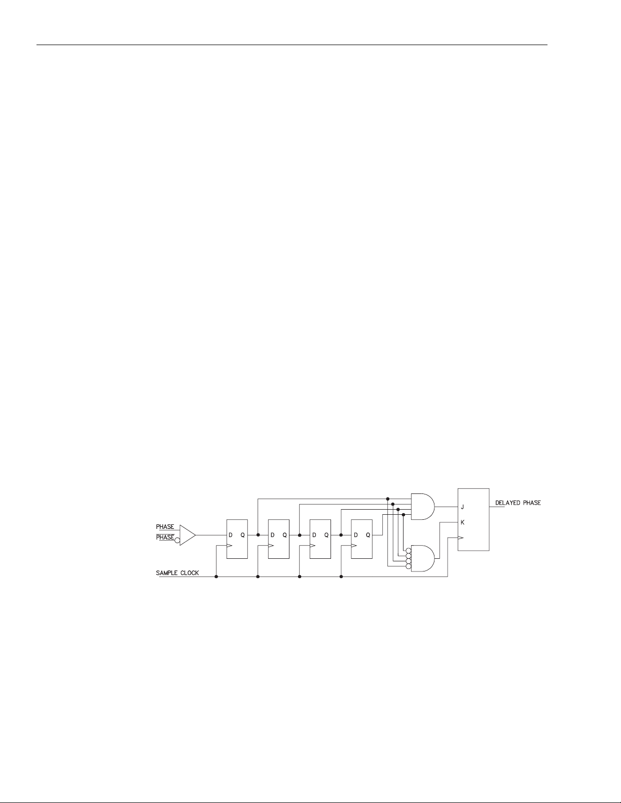
Each input line on the 5312 consists of a differential receiver pair followed by a 4-stage digital
filter. This digital filter is shown in simplified form in Figure 2-1. An input signal level must be
a valid HIGH for four sample clock cycles or a valid LOW for four sample clock cycles before
the filter output will change to the level of the input. This action prevents noise pulses of a duration shorter than (sample clock period)/4 from affecting the filter output signal.
To ensure that all valid input signals are transferred to the filter output, the sample clock period
should be approximately one eighth the width of the narrowest positive or negative input pulse.
In other words, the sample clock frequency should be eight times the input frequency assuming
a 50 percent duty cycle input signal.
One side effect of the digital filter is a 4-sample period delay from the time a signal arrives at the
input of the filter to the time it exits. For example, at the lowest sample clock frequency
(625 KHz) the filter delay is approximately 8 microseconds. At the maximum recommended
input pulse rate for this sample clock frequency, this is approximately 13 microseconds (assuming a 50 percent duty cycle). Thus, the filter delay is approximately 60 percent of the minimum
period input signal.
If delays of this length are unacceptable, a higher frequency sample clock may be used with the
loss of some noise immunity.
For example, if you select a sample clock rate of 1.25 MHz, the filter delay is approximately 4
microseconds or one third of the input signal period. However, the noise immunity of the filter is
degraded when compared with that obtained at a clock frequency of 625 KHz. When using a
clock period of 1.6 microseconds (1/0.625 MHz), intermittent noise pulses of greater than
6.4 microseconds will pass through the filter. Using a clock period of 0.8 microseconds
(1/2.5 MHz), intermittent noise pulses of greater than 3.2 microseconds will pass through the
filter.
Sample clock frequency selection is a trade-off between noise immunity and delay. For jumper
options, see Section 1.
Figure 2-1
Example of a 4-stage signal conditioning filter
Note: A side effect of using a digital filter is a 4-sample propagation delay.
Page 35

3
Interrupt Control
Page 36
3-2 Interrupt Control Model 5312B Technical Reference
Description of interrupt control
The 5312 uses an 8259A Programmable Interrupt Controller (PIC) to handle the interrupt
sources on the board, and must be programmed prior to operation. Each axis can generate two
interrupts: the first is a carry/borrow, signaling that an overflow or underflow has occurred, and
the second interrupt is caused when a valid index pulse has occurred.
The PIC may only be used in a nonvectored mode (polled). When a board-level interrupt is generated, the PIC must be polled to determine which interrupt was triggered. The PIC may be disabled by removing jumper W8.
Only the features of the 8259A PIC that are used by 5312 are discussed below. For complete
information on the 8259A PIC refer to the Peripheral Components Manual or the Microsystem
Components Handbook, Vol 1, published by Intel.
Figure 3-1 shows a functional block diagram of the 8259A PIC. On the 5312, the PIC is connected directly to the PC bus through jumper W14.
Figure 3-1
PIC block level diagram
INTA INT
CONTROL LOGIC
D7-D0
WR
AO
CAS0
CAS1
CAS2
SP/EN
RD
CS
DATA BUS
BUFFER
READ/WRITE
LOGIC
CASCADE BUFFER/
COMPARITOR
IN
SERVICE
REGISTER
(ISR)
INTERRUPT MASK REGISTER (1MR)
INTERNAL BUS
PRIORITY
RESOLVER
The 5312 uses an Intel 8259A and is directly connected to the PC bus through jumper W14.
Interrupt Request Rgtr (IRR), In-Service Rgtr (ISR)
The interrupts at the interrupt request input lines (IR0-IR5) are handled by the IRR and the ISR.
The IRR is used to store the interrupts requesting service, and the ISR is used to store the interrupts being serviced. Interrupts and IRR/ISR bits correspond to the format below.
Interrupt Request Register
INTERRUPT
REQUEST
REGISTER
(1RR)
AXIS A EOM
AXIS A EXT
AXIS B EOM
AXIS B EXT
AXIS C EOM
AXIS C EXT
NOT
NOT
IR6 IR2IR4 IR0IR7
IR3IR5 IR1
AXIS 1 CARRY/BORROW
AXIS 2 CARRY/BORROW
AXIS 3 CARRY/BORROW
AXIS 4 CARRY/BORROW
AXIS 1 INDEX
AXIS 2 INDEX
AXIS 3 INDEX
AXIS 4 INDEX
Page 37

D6 D2D4
Operating Mode
D0D7 D3D5 D1
INTERRUPT CODE
(SEE TABLE 3-1)
1: INTERRUPT HAS OCCOURED
Model 5312B Technical Reference Interrupt Control 3-3
Priority Resolver (PR)
The Priority Resolver (PR) block determines the priority of the bits set in the IRR. The highest
priority bit is selected and strobed into the corresponding ISR bit at the time of the poll
command.
Interrupt Mask Register (IMR)
The Interrupt Mask Register stores the bits that determine the interrupt lines to be masked. The
IMR operates on the IRR. Masking a higher priority input will not affect the interrupt request
lines of lower priority. Masking disables the interrupt for the masked input.
Interrupt output (INT)
The Interrupt Output (INT) signal indicates that the PIC has an interrupt request pending. This
signal can be routed to PC bus interrupt IRQ2 through IRQ7 (IRQ2 default) via W8. The poll
command causes interrupt status to be placed on the bus during the next read of the PIC.
PIC operation
Interrupt sequence, 80
x
86/80
The sequence of events during an interrupt when using an 80 x 86/80 x 88 CPU is as follows:
1. One or more of the interrupt request lines (IR0-IR7) are raised high setting the corresponding
IRR bit(s).
2. The PIC evaluates these requests and sends an interrupt request to the CPU provided that
jumper W8 is installed.
3. The interrupt is acknowledged by your program interrupt service routine by writing a poll
command (OCW3) to the PIC.
4. The CPU reads the PIC to obtain the priority level as shown below. After the read, the high
ISR bit is set, and the corresponding IRR bit is reset.
x
88 mode
Page 38

3-4 Interrupt Control Model 5312B Technical Reference
Table 3-1
Interrupt code
D2 D1 D0 Interrupt Request
0 0 0
0 0 1
0 1 0
0 1 1
1 0 0
1 0 1
1 1 0
1 1 1
The interrupt code returns the highest priority interrupt and sets the corresponding ISR bit.
5. The previous step completes the interrupt cycle. In the Automatic End-Of-Interrupt (AEOI)
mode, the ISR bit is reset on the read following the poll command. Otherwise, the ISR bit
remains set until an appropriate End-Of-Interrupt (EOI) command is issued.
IRQ0
IRQ1
IRQ2
IRQ3
IRQ4
IRQ5
IRQ6
IRQ7
End-of-interrupt command
Completing an interrupt
Operating modes
NOTE
After the priority level is read, the ISR bit must be reset. This is done with EOI command from
the host PC, or it can be done automatically in the AEOI mode. There are two forms of the EOI
command — Specific and Non-Specific. A Non-Specific EOI command resets the highest ISR
bit of those that were set, and a Specific EOI command can be issued to reset a specified ISR bit.
You have to provide an interrupt routine to trap IR7 interrupt glitches that appear as interrupt 7
requests. In the AEOI mode, the ISR bit for the interrupt being serviced is reset automatically at
the interrupt return in your interrupt routine.
If no IR lines are HIGH at step 4 of the sequence (i.e., the IR line went
HIGH to generate an interrupt request but then went away before it
was acknowledge), the PIC will issue an interrupt level 7. This causes
the call address or the vector byte to look as if IR7 generated an interrupt request. This is useful in determining whether an actual interrupt
request occurred or a noise spike tripped the request line.
Fully nested mode
This is the default mode entered after initialization unless another mode is programmed. In this
mode, interrupt requests are ordered in priority from 0 through 7 with 0 being the highest priority.
When a poll command is received and the priority level is read, the highest priority request is
placed on the data bus. The corresponding bit in the ISR is also set. It stays set until the CPU
issues an EOI command, or, if in AEOI mode, until the priority level is read. While the ISR bit is
set, all further interrupts of equal or lower priority are inhibited. Interrupts of higher priority will
issue an interrupt request (which will be acknowledged only if the PC has unmasked the interrupt).
Page 39

Model 5312B Technical Reference Interrupt Control 3-5
Special mask mode
This mode is similar to the fully nested mode except that when a bit in the ISR is set, it only
inhibits interrupt requests at that level. All other unmasked interrupt requests (lower as well as
higher) are enabled.
Specific rotation (specific priority)
The default priority of interrupts is IR0 (highest) through IR7 (lowest). This can be changed
using the set priority command. This command specifies one input as having the lowest priority
and fixing all other priorities. For example, if IR2 is specified as having the lowest priority, the
priority of interrupts will be: IR3 (highest), IR4, IR5, IR6, IR7, IR0, IR1, IR2 (lowest).
Automatic rotation (equal priority)
In this mode, a device, after being serviced, receives the lowest priority. Such a device requesting an interrupt would have to wait until all other devices have been serviced.
Non-vectored mode (poll command)
PIC programming
Initialization Command W ords (ICW)
The PIC must be polled for interrupt status. To do this, the poll command is written to the PIC,
and then the status is read. The PIC treats the read pulse as an INTA pulse. The interrupt is frozen from the write to the read.
The PIC accepts two types of command words from the CPU: Initialization Command Words
(ICW) and Operational Command Words (OCW).
Figure 3-2
PIC initialization sequence
ICW1
NO
(CIC4-0)
NEED
ICW4
YES
(CIC4-1)
ICW1
READY TO ACCEPT
INTERRUPT REQUESTS
Note: Bit D4 set assumes the next word issued will be ICW4.
Page 40
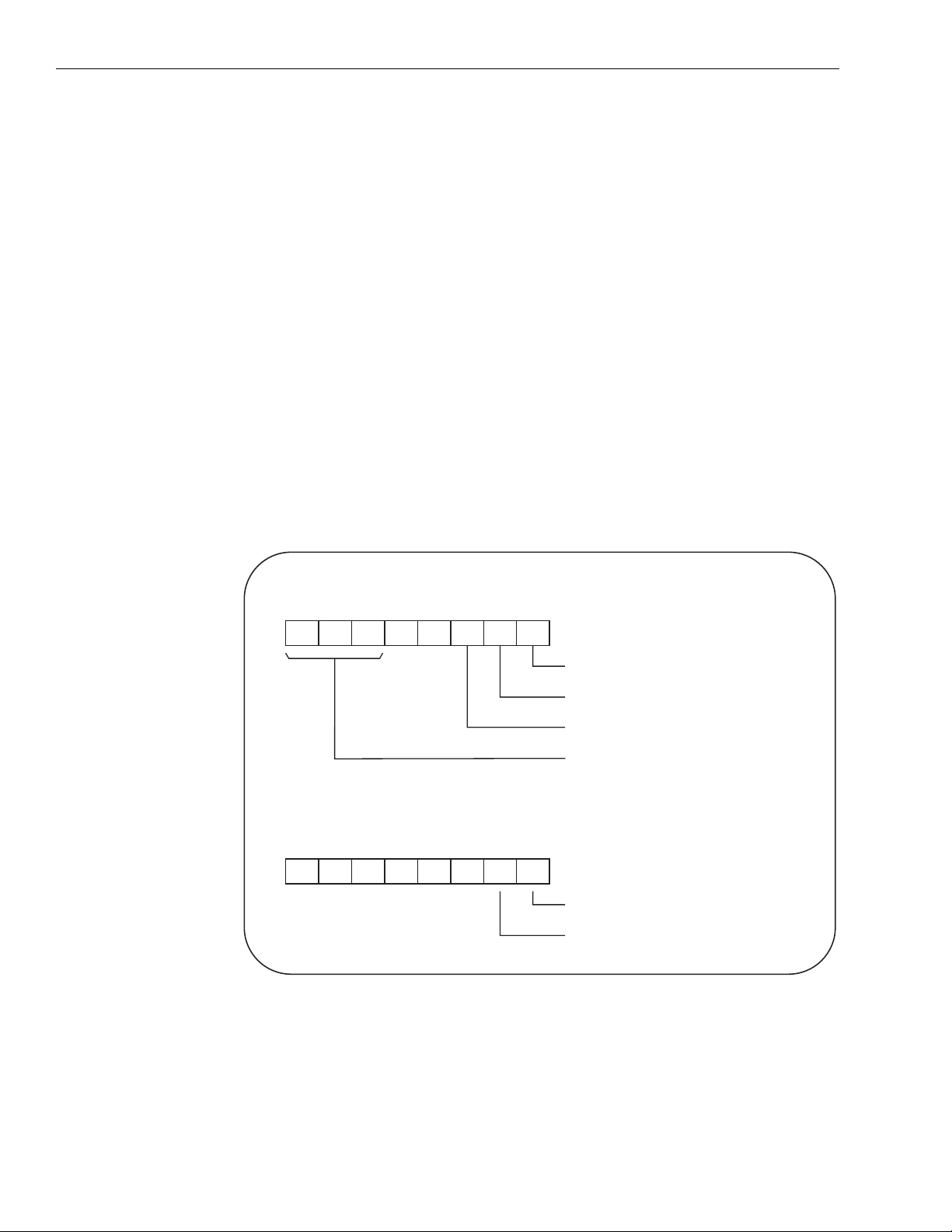
3-6 Interrupt Control Model 5312B Technical Reference
Before normal operation can begin, the PIC must be brought to a starting point by a sequence of
three bytes. Figure 3-2 shows the initialization sequence. Whene v er a command is written to the
PIC low port with bit D4 = 1, it is interpreted as ICW1. Register ICW1 starts the initialization
sequence during which the following automatically occur:
1. The IMR is cleared.
2. IR7 is assigned the lowest priority.
3. The slave mode address is set to 7.
4. Special Mask Mode is cleared.
5. Status Read is set to IRR.
6. If IC4 = 0, then all functions selected in ICW4 are set.
ICW2 is not used by the 5312. However, a value must be written to it to properly initialize the
PIC. Any value may be written since the value will have no effect on PIC operation.
ICW3 is not used by the 5312.
Writing to the ICW4 completes the initialization sequence.
ICW1 format and description
Figure 3-3
PIC ICW format
ICWI
ICWI
(WRITTEN TO THE PIC LOW PORT)
D6
D7
A7
D7
0
D5
A6
A5
(WRITTEN TO THE PIC HIGH PORT)
D6
D5
0
0
D4
I
D4
0
D3
D3
D2
0
ADI
D2
0
0
D1
SGL
D1
AE0I
D0
IC4
D0
UPM
I : ICW4 NEEDED
0 : ICW4 NOT NEEDED
I : SINGLE
0 : CASCADE MODE
I : CALL ADDRESS INTERVAL 4
0 : CALL ADDRESS INTERVAL 8
I : A7-A5 OF INTERRUPT VECTOR
0 : ADDRESS (8080/8085 MODE ONLY)
I : I8086/8088 MODE
0 : 8080/8085 MODE
I : AUTO E0I
0 : NORMAL E0I
Note: Write ICW1 to the PIC low port and ICW4 to the PIC high port depending on how you initialize.
Figure 3-3 shows the format for ICW1 and ICW4. Set the bits for the 5312 to the PIC low port in
the following manner:
D5-D7 (A7-A5): May be set or cleared. This bit has no impact on the operation of the 5312.
D2 (ADI): May be set or cleared. This bit has no impact on the operation of the 5312.
D1 (SNGL): Set this bit.
Page 41

Model 5312B Technical Reference Interrupt Control 3-7
DO (IC4): If ICW4 is needed, set this bit. ICW4 is needed if the CPU is an 80x86/80x88 or if
AEOI mode is desired.
ICW4 format and description
ICW4, written to the PIC high port, is read only if D4 of ICW1 is set. Set the data bits in the following manner:
D0 (UPM): Set this bit for operation in 8086 or 8088 mode. Clear this bit for operation in 8080
or 8085 mode.
D1 (AEOI): Set this bit for AEOI mode, and clear it for normal EOI.
Operation Command W ords (OCW)
These are the words that command the PIC to operate in various interrupt modes. The OCW can
be written to the PIC anytime after initialization. Figure 3-4 shows the format for OCW.
Page 42

3-8 Interrupt Control Model 5312B Technical Reference
Figure 3-4
PIC OCW format
Note: Write to the OCW at any time after initialization.
OCW1 format and description
Written to the PIC high port, OCW1 sets and clears the mask bits in the Interrupt Mask Register
(IMR). M7-M0 represent the eight mask bits for IR7-IR0, respectively. M = 1 means that the
input is masked (inhibited), while M = 0 means that the input is enabled. Since IR6 and IR7 are
not used by the PIC, set M6 and M7. Reading OCW1 through the PIC high port returns the interrupts that are masked.
Page 43

Model 5312B Technical Reference Interrupt Control 3-9
OCW2 format and description
The bits in OCW2, written to the PIC low port, are defined as follows:
D7 (R): Used to control all PIC rotation operations. If R is set, a form of priority rotation will be
executed depending on the operation selected.
D6 (SL): Used to select a specific level for a given operation. If set, L0-L2 are enabled, and the
operation selected will be executed on the specified interrupt level.
D5 (EOI): Used for all EOI commands (except AEOI). If set, a form of EOI will be executed.
D0-D2 (L0-L2): Designates an interrupt level (0-7) to be acted upon for the operation selected
by the EOI, SL, and R bits. L0-L2 are enabled or disabled by the SL bit.
All the possible operations by OCW2 are shown in Figure 3-6. A brief description of each is
given below.
OCW2 commands
Non-specific EOI command: Of the ISR bits that are set, the one with the highest priority is
cleared.
Specific EOI command: The ISR bit specified by LO-L2 is cleared.
Rotate on non-specific EOI command: Same as non-specific EOI, except that when an ISR bit
is cleared, its corresponding IR is assigned the lowest priority.
Rotate in AEOI: Same as rotate on non-specific EOI command, except that priority rotation is
done automatically after the last INTA pulse. Setting the bit enters this mode, and clearing the
bit exits this mode.
Rotate on specific EOI: Same as specific EOI, except that after the specified ISR bit is cleared,
its corresponding IR is assigned the lowest priority.
Set priority command: The specified bit is assigned the lowest priority.
OCW3 format and description
The bits in OCW3, written to the PIC low port, are defined according to the following:
D6 (ESMM): Enable special mask mode. When set, it enables the SMM bit (see below) to set
or reset the special mask mode. When ESMM is cleared, the SMM bit becomes a don't care.
D5 (SMM): Special mask mode. If ESMM and SMM are set, the PIC will enter the special
mask mode. If ESMM is set and SMM is cleared, the PIC will revert to normal mask mode.
Page 44

3-10 Interrupt Control Model 5312B Technical Reference
ESMM SMM Mode
1
1
D5 (SMM): Special mask mode. If ESMM and SMM are set, the PIC will enter the special
mask mode. If ESMM is set and SMM is cleared, the PIC will revert to normal mask mode.
D2 (P): Polled mode. If set, the next read of the PIC low port will return the highest priority
level requesting the interrupt if an interrupt has occurred. See Figure 3-3.
D1 (RR): Read register. If set, the next read of the PIC low port will return IIR and ISR status,
depending on the RIS bit (see below). If RR is cleared, the RIS bit becomes a don't care .
1
0
Special Mask Mode
Normal Mask Mode
NOTE
D0 (RIS): If P = 0, RR = 1, and RIS = 0, the next read of the PIC low port will return the IRR
status. If P = 0, RR = 1, and RIS = 1, the next read of the PIC low port will return the ISR status.
P RR RIS Next Read of Low Port
0
0
NOTE
If P=1 and RR=1, the poll command will override the read register
command.
1
1
After issuing a poll command, do not read the Mask Register (PIC
high port) before reading the poll status (PIC low port).
0
Return IIR Status
1
Return ISR Status
Page 45

A
PC I/O and
Interrupt Mapping
Page 46

A-2 PC I/O and Interrupt Mapping Model 5312B Technical Reference
PC I/O map
Table A-1 shows how the PC is typically mapped. Obviously, this list does not include every
possible type of board available. Check the boards in your system to be certain which addresses
are used.
Table A-1
PC I/O map
Address # of Bytes PC XT AT
100h to 1EFh
1F0h to 1F8h
1F9h to 1FFh
200h to 20Fh
210h to 217h
218h to 21Eh
21Fh
220h to 257h
258h to 25Fh
260h to 277h
278h to 27Fh
280h to 2AFh
2B0h to 2DFh
2E0h
2E1h
2E2h to 2E3h
2E4h to 2F7h
2F8h to 2FFh
300h to 31Fh
320h to 32Fh
330h to 347h
348h to 357h
358h to 35Fh
360h to 36Fh
370h to 377h
378h to 37Fh
380h to 38Fh
390h to 393h
394h to 39Fh
3A0h to 3AFh
3B0h to 3BFh
3C0h to 3CFh
3D0h to 3DFh
3E0h to 3EFh
3F0h to 3F7h
3F8h to 3FFh
240
9
7
16
8
7
1
56
8
24
8
48
48
1
1
2
20
8
32
16.00
24
16
8
16
8
8
16
4
12
16
16
16
16
16
8
8
Write Only
Write Only
Write Only
Game Controller
Open
Open
Open
Open
Intel Above Board
Open
LPT2
Open
Alternate EGA
Open
GPIB
Data Acquisition
Open
COM2
Prototype Area
Fixed Disk Fixed Disk Open
Open
DCA 3270
Open
PC Network
Open
LPT1
SDLC; Binary Synchronous Communications
Cluster
Open
Binary Synchronous Communications
Monochrome Display Adapter
Enhanced Graphics Adapter
Color Graphics Adapter
Open
Diskette Controller
COM1
Open
Open
Open
Game Controller
Expansion Unit
Open
Reserved
Open
Fixed Disk
Open
Game Controller
Open
Open
Open
Page 47

Model 5312B Technical Reference PC I/O and Interrupt Mapping A-3
Table A-2 shows how interrupts are typically mapped in a PC. Check the boards in the PC to
determine exactly which interrupts are being used. The printer ports LPT1 and LPT2 hav e inter rupts available to them, but under normal operation these interrupts are not used.
Table A-2
PC interrupt map
IRQ
IRQ2
IRQ3 COM2
IRQ4 COM1
IRQ5 Fixed Disk Fixed Disk LPT2
IRQ6 Floppy Disk
IRQ7 LPT1
IRQ10 Not available Not available Open
IRQ11 Not available Not available Open
IRQ12 Not available Not available Open
IRQ14 Not available Not available Fixed Disk
PC XT AT
Reserved Reserved IRQ9
EGA Display Adapter
PC Network
PC Network
Binary Synchronous Communications
Cluster
SLDC
Binary Synchronous Communications
SDLC
Cluster
IRQ15 Not available Not available Open
Page 48

B
Tech Bulletins and
Application Notes
Page 49

B-2 Tech Bulletins and Application Notes Model 5312B Technical Reference
Timer application in velocity mode
The 7166 counter chip used on the 5312 board will count quadrature inputs down to 208 nanoseconds or 4.8MHz. However, counting is actually limited to 10MHz / 8 or 1.25MHz per channel. This yields a maximum quadrature count rate of 2.5MHz and an up/down (or count and
direction) rate of 10MHz.
To use the 5312 in a timer application, position information has to occur at prescribed and precise time intervals.
We will assume a resolution of n counts per unit of dimension, and axes 0 to 2 will be used to
count absolute dimension information. Axis 3 will be used as an interval timer. In this mode,
axis 3 will capture the counts of axes 0 to 2 and also will generate an interrupt to the host computer. When the interrupt occurs, the host CPU will need to store data from axes 0 to 2 to RAM
or perform other calculations (such as velocity).
Timer accuracy can be set in 0.1 microsecond increments. Since capturing the counts are triggered by hardware, the software only has to respond to the time interval interrupts allowing the
host processor to do other housekeeping while in between the interrupt calls.
Setting up axis 3 as an interval timer
1. Remove jumpers W17, W24, W22, W26, W29, W33, W36, W37, W44, W46, and W48.
2. Jumper (2-3) on W45, W47, and W49.
3. Jumper W50 is a don’t care.
4. Wirewrap W36 (3) to W22 (1) to W24 (1) to W17 (1) to W36 (2).
5. Wirewrap W23 (7) to W33 (2).
6. W irewrap W37 (2) to W19 (1). If axis 3 counts in the wrong direction, remove the wirewrap
from W19 (1) and attach it to W19 (3).
Only 1 LCTR pull-up resistor can be driven by the borrow output of a 7166 chip. If you need to
trigger more than one axis, remove the excess pull-up resistor legs from their respective connections. (Refer to the 5312 schematic for pull-up resistor numbers attached to the wires going to
W24 and W17.) This will to maintain a TTL current level in the 7166 borrow output under
4mA.
Set axis 3 as a pulse and direction counter in the divide by n mode. Preset axis 3 counter with
the correct number of counts for the time interval desired using the appropriate sample clock frequency (10MHz for this example). By wirewrapping the sample clock, W23 (3), to axis 2 channel A counter input, W33 (2), each count input will trigger every 0.1 microseconds. Therefore,
to set the timer interval to 2 milliseconds, preset the counter to 19,999.
Set: MC = 35h, ICR = 48h, OCCR = 84h, QR = C0h
Subtracting 1 from the count is necessary because the counter triggers on the rollover or borrow
pulse (transition from 0 to FFFFFFh). Although this only yields an error of 100 nanoseconds, if
not corrected, error accumulation eventually becomes significant. Attempt to be as precise as
possible.
Once the hardware is configured, the software does the rest. Software provides the driver routines to collect the data and set up interrupts with the least possible effort.
Page 50

C
Circuit Diagrams
Page 51

C-2 Circuit Diagrams Model 5312B Technical Reference
Page 52

Index
A
Automatic rotation 3-5
B
Base addressing 1-4
C
Circuit Diagrams C-1
Completing an interrupt 3-4
Connector pinouts 1-13
D
Description 1-2
Description of interrupt control 3-2
E
End-of-interrupt command 3-4
F
Fully nested mode 3-4
Interrupt output (INT) 3-3
Interrupt Request Rgtr (IRR),
In Service Rgtr (ISR) 3-2
Interrupt selection 1-10
Interrupt sequence, 80x86/80x88 mode 3-3
Introduction and intstallation 1-1
M
Master Control Register (MCR) 2-3
N
Non-vectored mode (poll command) 3-5
O
OCW1 format and description 3-8
OCW2 commands 3-9
OCW2 format and description 3-9
OCW3 format and description 3-9
Operating modes 3-4
Operation command words (OCW) 3-7
Operation and programming 2-1
Output/Counter Control Register (OCCR) 2-4
Output Status Register (OSR) 2-6
I
ICW1 format and description 3-6
ICW4 format and description 3-7
Indirect addressing 1-5
Initialization Command Words (ICW) 3-5
Input Control Register (ICR) 2-4
Installation 1-11
Interrupt control 3-1
Interrupt Mask Register (IMR) 3-3
P
PC I/O and interrupt mapping A-1
PC I/O map A-2
PIC operation 3-3
PIC programming 3-5
Power considerations 1-12
Priority Resolver (PR) 3-3
Programming 2-2
i-1
Page 53

Q
Quadrature Register (QR) 2-5
R
Reading the Output Latch register (OL) 2-3
S
Selecting a sample clock frequency 2-8
Selecting an index option 1-8
Selecting the card configuration 1-9
Setting the jumpers 1-3
Setting up axis 3 as an interval timer B-2
Special mask mode 3-5
Specific rotation (specific priority) 3-5
T
Tech bulletins and application notes B-1
Technical specifications 1-3
Termination resistors 1-6
Theory of operation 2-2
Timer application in velocity mode B-2
Typical programming examples 2-6
W
Wait states 1-11
Writing the Command Register (CR) 2-3
Writing the Preset Register (PR) 2-2
i-2
Page 54

Keithley Instruments, Inc.
28775 Aurora Road
Cleveland, Ohio 44139
Printed in the U.S.A.
 Loading...