

Page 1
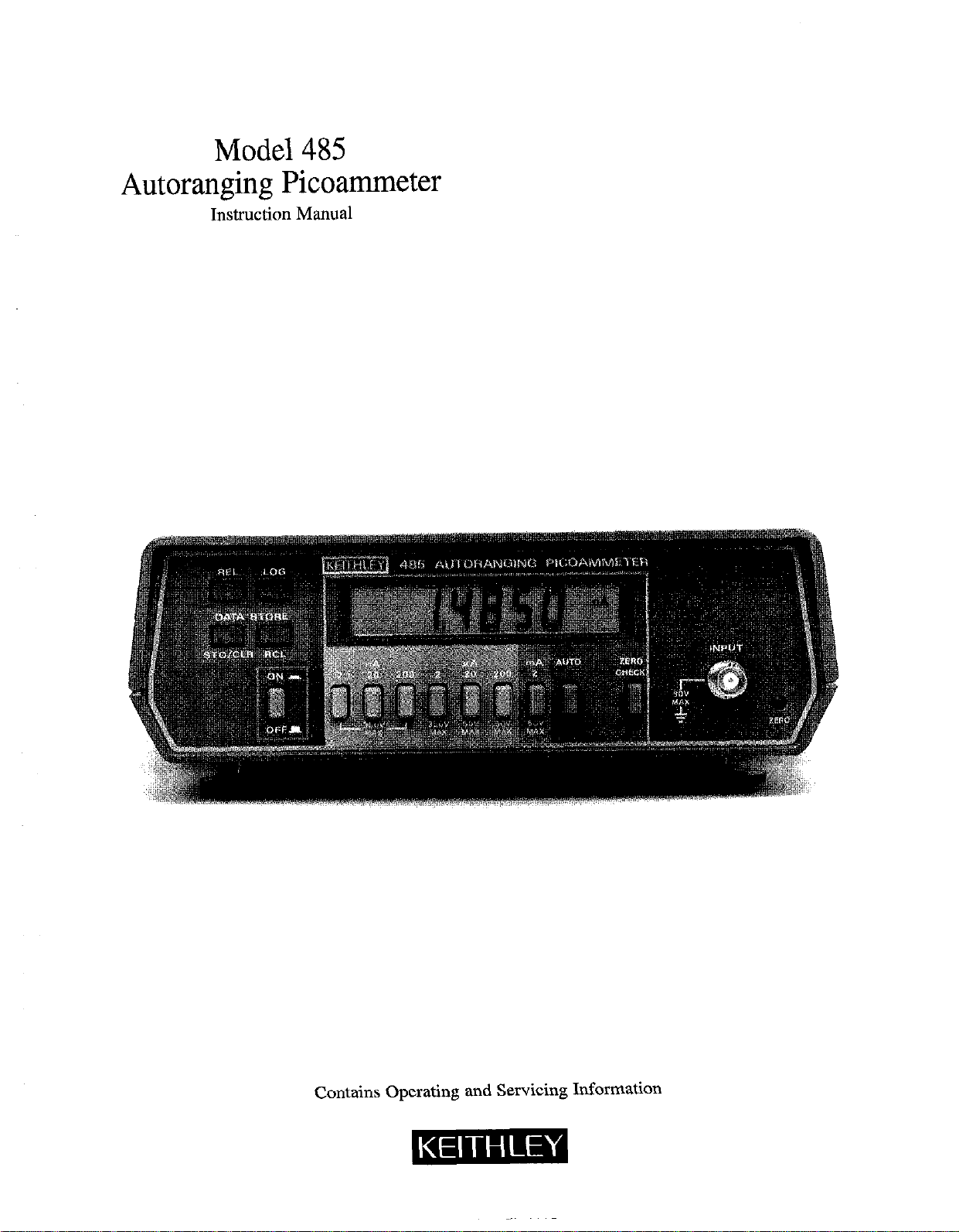
Model 485
Autoranging Picoammeter
Instruction Manual
Contains Operating and Servicing Information
Page 2

WARRANTY
Keithley Instruments, Inc. warrants this product to be free from defects in material and workmanship for a period of 1 year from date of
shipment.
Keithley Instruments, Inc. warrants the following items for 90 days from the date of shipment: probes, cables, rechargeable batteries,
diskettes, and documentation.
During the warranty period, we will, at our option, either repair or replace any product that proves to be defective.
To exercise this warranty, write or call your local Keithley representative, or contact Keithley headquarters in Cleveland, Ohio. You will
be given prompt assistance and return instructions. Send the product, transportation prepaid, to the indicated service facility. Repairs
will be made and the product returned, transportation prepaid. Repaired or replaced products are warranted for the balance of the original warranty period, or at least 90 days.
LIMITATION OF WARRAN-IY
This warranty does not apply to defects resulting from product modification without Keithley’s express written consent, or misuse of
any product or pwt. This warranty also does not apply to fuses, software, non-rechargeable batteries, damage from battery leakage, or
problems arising from normal wear or failure to follow instructions.
THIS WARRANTY IS IN LlBU OF ALL OTHER WARRANTIES, EXPRESSED OR IMPLIED, INCLUDING ANY IMPLIED
WARRANTY OF MERCHANTABILITY OR FITNESS FOR A PARTICULAR USE. THE REMEDIES PROVIDED HEREIN ARE
BUYER’S SOLE AND EXCLUSIVE REMEDIES.
NEITHER KBITHLEY INSTRUMENTS, INC. NOR ANY OF ITS EMPLOYEES SHALL BE LIABLE FOR ANY DIRECT, INDIRECT, SPECIAL, INCIDENTAL OR CONSEQUENTIAL DAMAGES ARISING OUT OF THE USE OF ITS INSTRUMENTS AND
SOFTWARE EVEN IF KEITHLEY INSTRUMENTS, INC., HAS BEEN ADVISED IN ADVANCE OF THE POSSIBILITY OF
SUCH DAMAGES. SUCH EXCLUDED DAMAGES SHALL INCLUDE, BUT ARE NOT LIMITED TO: COSTS OF REMOVAL
AND INSTALLATION, LOSSES SUSTAINED AS THE RESULT OF INJURY TO ANY PERSON, OR DAMAGE TO PROPERTY
Keithley Instruments, Inc. - 28775 Aurora Road *Cleveland, OH 44139~216-248-0400 -Fax: 216-248-6168 * http://www.keithley.com
Page 3

Model 485 Autoranging Picoammeter
Instruction Manual
0 1984, Keithley Instruments, Inc.
Test Instrumentation Group
All rights reserved.
Cleveland, Ohio, U.S.A.
January 1990, Sixth Printing
Document Number: 485-901-01 Rev. F
Page 4
SPECIFICATIONS
ACCURACY I1 YEAR,
lW28~C
RANGE
2nA
20
200
RESOLUTION
“A 1 PA
“A 10 pA
O.lpA
2 PA 100 PA
20
!A 1 nA
200
,‘A 10 “A
2mA
,NP”T VOLTAGE BURDEN: Less than 200&V.
RANQING: Manual or autoranging.
AUTORANGING TIME: Average 250ms per range.
SmLlNG TIME AT DISPLAY: Less than 1 second to within 2 co”nts on
fixed range.
CONVERSION PERIOD: 300,“s.
TEMPERATURE COEFFICIENT 10°-160C B 26°-50”C,: f10.1 x BP-
plicable sccuracy specification) per OC.
MAwMUM COMMON MODE VOLTAGE: 30V rms. DC to 60Hz sine
100 “A
* l%rdg + countslt
0.4 + 4
0.4 + 1
0.2 + 1
0.15 + 1
0.1 + 1
0.1 +1
0.1 +1
WWB.
ANALOG OUTPUT:
Output Voltage: + IV = - 10000 co”ntf.. mept + 1OOmV = - 10000
mints 0” 2nn range.
OUtput tIea,*tance: 10000.
REL: Pushbutton allows zeroing of an range readings. Allows relative
readings to be made with respect to baseline value. Front panel ~nnuncistor
indicates REL mode.
DATA STORE and MINIMAX: 100 reading storage capacity: records data
at one of six selectable rates from 3 readings/second to 1 reading/hour, or
by manual triggering. Also detects and stores maximum and minimum
readings comin”““sIY while in the data store mode.
LOG: Displays logarithm (base 101 of the absolute value of the measured C”F
rent Iexamples: -3.000 = *ImA; -6.301 = +O.$Al.
IEEE-488 BUS IMPLEMENTATION (Option 48631
MULTILINE COMMANDS: DCL, SDC, GET, GTL, “NT. UNL. SPE. SPD.
UNILINE COMMANDS: IFC, REN EO,. SRC. ATN.
INTERFACE FUNCTIONS: SHl. AH,, T5. TEO. L4, LEO. SRI, RL2,
PPO. DCl, DTI, CO, El.
PROGRAMMABLE PARAMETERS: Zero Check. Range, REL. LOG, Trig-
ger, Calibration. EO,, SRO, Status. 0”tp”t Format. Terminator.
ANALOG REJECTION
RISE TIME RATIO
I10 .SO%, IS0 or EOHz, INPUTt
60ms
60iTlS
6rnS
3ms
3ms
lms
lms
GENERAL
DISPLAY: 4% digit LCD, 0.5” height: polarity. range and staf”s indication.
OVERRANGE INDICATION: “OL” displayed.
CONNECTORS:
Input: ENC.
Analog Output: Banana Jacks.
OPERATING ENVIRONMENT: 0-50.X. less than 70% R.H. up to 35’C:
linearly derate 3% R.H./OC up to 5OOC.
STORAGE ENVIRONMENT: -25O to +BO”C
POWER: lOF,-125V or 210.250V (switch selected,. go-llOV available.
SO-6OHr. 12 VA.
DIMENSIONS, WEIGHT: 65mm high Y 235mm wide x 275mm deep.
(3%” x 9%” x lO%“,.
Net Weight: 1 .Skg I4 Ibs.)
ACCESSORIES AVAILABLE:
Model 1010:
Model ,017:
Model 1664:
Mods, 1758:
Model 4801:
Model 4603:
Model 4653:
Model 7006-3:
Model 7006-6:
Model 6573:
NORMAL MODE
7OdB
7OdB 350Vdc
65dB 350Vdc
6FdB 350Vdc
65dB 5O”dc
65dB 5OVdc
55dB
Single Rack Mounting Kit
Dual Rack Mounting Kit
Hard Shell Carrying Case
Rechargesble Battery Pack
Low Noise Input Cable (4ft.l. BNC to ONC
Low Noise Cable Kit
IEEE-486 Interface
IEEE-466 Digital Cable 13ft.b
IEEE-468 Digital Cable 16 ft.1
IEEE-488 Interface for IBM PC
MAXIMUM
CONTINUOUS
350”dC
5OVdc
Specifications subject to change without notice.
Page 5
1.1
1.2
1.3
1.4
1.5
1.6
1.7
1.8
TABLE OF CONTENTS
SECTION l-GENERAL INFORMATION
Introduction.
Getting Started
Unpacking and Inspection
Specifications
Warranty Information.
Manual Addenda
Safety Symbols and Terms
Optional Accessories
........................... ...... ......
.........................
................
..........................
...................
.......................
...............
....................
...... ......
...... ......
......
...... ......
...... ......
...... ......
...... ......
......
......
......
......
......
......
. ......
......
......
......
......
......
......
......
......
......
......
l-1
1-l
l-l
l-l
l-l
1-2
1-2
l-2
2.1
2.2
2.2.1
2.2.2
2.2.3
2.3
2.4
2.4.1
2.4.2
2.4.3
2.4.4
2.5
2.6
2.7
2.7.1
2.7.2
2.7.3
2.7.4
2.75
2.7.6
2.7.7
2.8
2.8.1
2.8.2
2.8.3
2.8.4
2.8.5
SECTION Z-BENCH OPERATION
introduction ...............................................................................
PreparationforUse
Line Power ..............................................................................
Battery Pack Power .......................................................................
BatteryCharging
TntBail ....................................................................................
Model 485 Familiarization
Display
FrontPanelControls
InputConnector ..........................................................................
AnalogOutputConnectors
Error Messages
EnvironmentalCondition .....................................................................
BasicBenchMeasurements
Power-Up ...............................................................................
Zero Check ..............................................................................
Current Measurements ....................................................................
RelativeMode
LOGMode ...............................................................................
Inverting Analog Output ...................................................................
MIN/MAXand 100 Point Data Store
MeasurementConsiderations
SourceResistance ........................................................................
SourceCapacitance
LeakageResistance .......................................................................
ZeroTimeStability
Groundingconsiderations
..................................................................................
..........................................................................
.........................................................................
....................................................................
.......................................................................
.................................................................
.............................................................................
..................................................................
...........................................................................
.........................................................
.................................................................
.......................................................................
........................................................................
..................................................................
2-l
2-l
2-l
2-l
2-l
2-1
2-l
2-l
2-2
2-2
2-2
2-2
2-3
2-3
2-4
2-4
2-4
2-4
2-5
2-5
2-6
2-6
2-6
2-7
2-8
2-8
2-8
2.9
2.9.1
2.9.2
2.9.3
2.9.4
2.9.5
3.1
3.2
i::
3.5
Applications
Op Amp Offset Current
FET Gate Leakage and Channel Current.
Insulation Leakage Currents and High Resistance.
Phototube, Photodiode and Beam Currents
Resistivity Tests
SECTION 3-PERFORMANCE VERIFICATION
Introduction ......................................
Environmental Conditions
Recommendrsd Test Equipment
Initial Conditrons
Verification Procedure
................................................. .........................
......................................
.......................
.....................
............................................
...........................
......................
...................................
..............................
................
.........................
.........................
.........................
.........................
.........................
..................
,,....
,,....
..................
..................
..................
..................
3-l
3-l
,. 3-l
3-1
3-l
i
Page 6
4.1
4.2
4.3
4.3.1
4.3.2
4.3.3
4.3.4
4.3.5
4.4
4.4.1
4.4.2
4.4.3
4.4.4
4.5
4.6
4.7
5.1
5.2
5.3
5.4
5.4.1
5.4.2
5.4.3
5.4.4
5.4.5
5.5
5.6
5.6.1
5.62
5.63
5.6.4
5.6.5
5.7
5.8
5.9
TABLE OF CONTENTS (CONT.)
SECTION 4-THEORY OF OPERATION
Introduction ...............................................................................
Overall Functional Description. ................................................................
AnalogCircuitry ............................................................................
Current-to-Voltage Converter ...............................................................
Multiplexer ............................................................................
InputBufferAmplifier .....................................................................
-2VReferenceSource .....................................................................
AIDConverter.. ......................................................................... 4-3
Digital Circuitry .............................................................................
Microcomputer ...........................................................................
Address Decoding ........................................................................
PIA .....................................................................................
DisplayBoard.. ..........................................................................
Digital Calibration ...........................................................................
PowerSupply ..............................................................................
Model 1758 Battery Option ...................................................................
SECTION 5-MAINTENANCE
Introduction ...............................................................................
Top Cover Removal/Installation ...............................................................
Battery Pack (Model 1758) Installation
Front Panel Calibration ......................................................................
Recommended Calibration Equipment.
CalibrationJumper ........................................................................
Environmental Conditions ..................................................................
Calibration Procedure. .....................................................................
CalibrationStorage ........................................................................
Calibration Over IEEE-488 Bus .................................................................
Troubleshooting ............................................................................
Recommended Test Equipment .............................................................
Self Diagnostic Program ...................................................................
Power Supply and Battery Pack (Model 1758) Checks
A/D Converter and Display .................................................................
SignalConditioning .......................................................................
Input Amplifier NJ105) Balancing ..............................................................
LineFuseReplacement ......................................................................
Special Handling of Static Sensitive Devices.,
.........................................................
.......................................................
...................................................
4-2
...........................................
4-l
4-l
4-l
4-1
4-2
4-3
4-4
4-4
4-4
4-4
4-4
4-4
4-4
4-4
5-I
5-l
5-l
5-l
5-1
5-2
6-2
5-2
5-2
5-3
5-3
5-3
5-3
5-6
5-6
5-7
5-7
5-7
5-8
6.1
if
6.4
6.5
SECTION B-REPLACEMENT PARTS
Introduction ...............................................................................
ReplaceableParts ...........................................................................
Ordering Information ........................................................................
FactorySen/ice .............................................................................
Component Location Drawings and Schematic Diagrams
ii
..........................................
6-l
6-l
6-l
6-l
6-l
Page 7
LIST OF ILLUSTRATIONS
2-1
2-2
2-3
2-4
2-5
2-6
2-7
Z-8
2-9
2-10
3-l
4-l
4-2
4-3
4-4
4-5
5-I
5-2
6-l
6-2
6-3
6-4
6-5
6-6
6-7
6-8
Model485FrontPanel ....................................................................... 2-2
Model 465 Inverting Analog Output
Simplified Model for Input Signal Conditioning
Test Fixture Guarding ....................................................................... 2-8
LeakageTestSetUpUsingModel6104 ........................................................ 2-8
Op Amp Input Offset Currents Measurement
F5T Gate Leakageand Channel Currents Measurement.
Insulation Leakage Currents end High Resistances Measurement .................................... 2-9
Set Up to Measure Photomultiplier, Photodiode end Beam Currents .............................. ,, 2-9
ResistivityTestSetUp
Shielded Test Fixture ........................................................................ 3-2
Simplified Block Diagram ..................................................................... 4-l
Current-to-Voltage Converter
Simplified Schematic of the Multiplexer
Simplified Schematic of the Input Buffer Amplifier
AIDConverter
Segmentldentification
JumperLocations ...........................................................................
Model485MiscelianeousParts
Display Assembly
Mother Board, Component Location Drawing. Dwg. No. 485-100
Mother Board, Schematic Diagram, Dwg. No. 485-106., .......................................... 6-9
Display Board, Component Location Drawing, Dwg. No. 485.110 ................................... E-13
Display Board, Schematic Diagram, Dwg. No. 485-116
Model 1758 Battery Peck, Component Location Drawing, Dwg. No. 1758-100 ......................... 615
Model 1758 Battery Peck, Schematic Diagram, Dwg. No. 1768-106 ................................. 6.16
.............................................................................
......................................................................
.......................................................................
...........................................................................
........................................................... 2-6
..................................................
....................................................
...........................................
.................................................................
.........................................................
................................................
...............................................................
...................................
............................................
2-7
2-8
2-9
Z-IO
4-2
4-2
4-2
4-3
5-4
5-7
6-2
6-3
6-7
6-14
iii
Page 8
LIST OF TABLES
2-1
2-2
2-3
3-1
3-2
5-1
5-2
5-3
5-4
5-5
5-6
5-7
5-8
6-1
6-2
83
8-4
Error Messages.. ..........................................
Range, Accuracy and hlaximum Allowable Inputs
Equivalent Input Resistance With Zero Check Enabled
Recommended Test Equipment ..............................
RangeAccuracy ...........................................
Range Calibration ..........................................
Recommended Troubleshooting Equipment
TroubleshootingModes .....................................
Power Supply Checks and Battery Pack (Model 1758) Checks
A/DConverterChecks ......................................
DisplayBoardChecks ......................................
OffsetJumparSetUp ......................................
Static Sensitive Devices ....................................
Mother Boerd, Parts List ....................................
Display Board, Parts List ....................................
Model 1758 Battery Pack, Parts List ...........................
Model485SperePartsList ..................................
...............
............
....................
.....
.......
.......
.......
.......
2-3
2-3
2-4
3-l
3-2
5-3
5-3
5-5
6-6
6-6
5-7
5-7
5-8
6-4
6-13
6-15
6-17
iv
Page 9

SAFETY PRECAUTIONS
The following safety precautions should be observed before operating the Model 485.
This instrument is intended for use by qualified personnel who recognize shock hazards and are familiar
with the safety precautions required to avoid possible injury. Read over the manual carefully before
operating this instrument.
Exercise extreme caution when a shock hazard is present at the instrument’s input. The American
National Standards Institute (ANSI) states that a shock hazard exists when voltage levels greater than
30V rms or 42.4V peak are present. A good safety practice is to expect that a hazardous voltage
is present in any unknown circuit before measuring.
Do not exceed 30V rms between the input connector shell and earth ground.
Inspect the test leads for possible weer, cracks or breaks before each use. If any defects are found,
replace with test leads that have the same measure of safety as those supplied with the instrument.
For optimum safety do not touch the test leads or the instrument while power is applied to the circuit
under test. Turn the power off and discharge all capacitors, before connecting or disconnecting the instrument.
Do not touch any object which could provide a current path to the common side of the circuit under
test or power line (earth) ground. Always make measurements with dry hands while standing on a dry,
insulated surface, capable of withstanding the voltage being measured.
Do not exceed the instrument’s maximum allowable input as defined in the specifications and operation
section.
Safe operation and good measurement practice dictates use of an external resistor when necessary to
limit input currents to less than 3mA.
Page 10

Model 485 Addendum
me following idormation is supplied as a supplement to tfi manual k order to prmide the user
with the latest tiprovements. It is recommended that vefication tio~tion k added to Section 3
of the Model 485 Instiction Manual and c&bration tifomatimr be added to Section 5.
~is addendum contatis complete procedures for vefi@g and cahhatig the Model 485 ustig the
WltMq Model 2& Cdibmtor/Somce. Complete sepmate pmcedmes a pmtided for @otig di@ti
calibration horn either the hont panel or over the IEEE+8 bus. Dgitd ctibration over the bus is
automated ustig a BASIC pro~am mn @ the W 85 computer.
PA-2w Rev. A / 149
Page 11
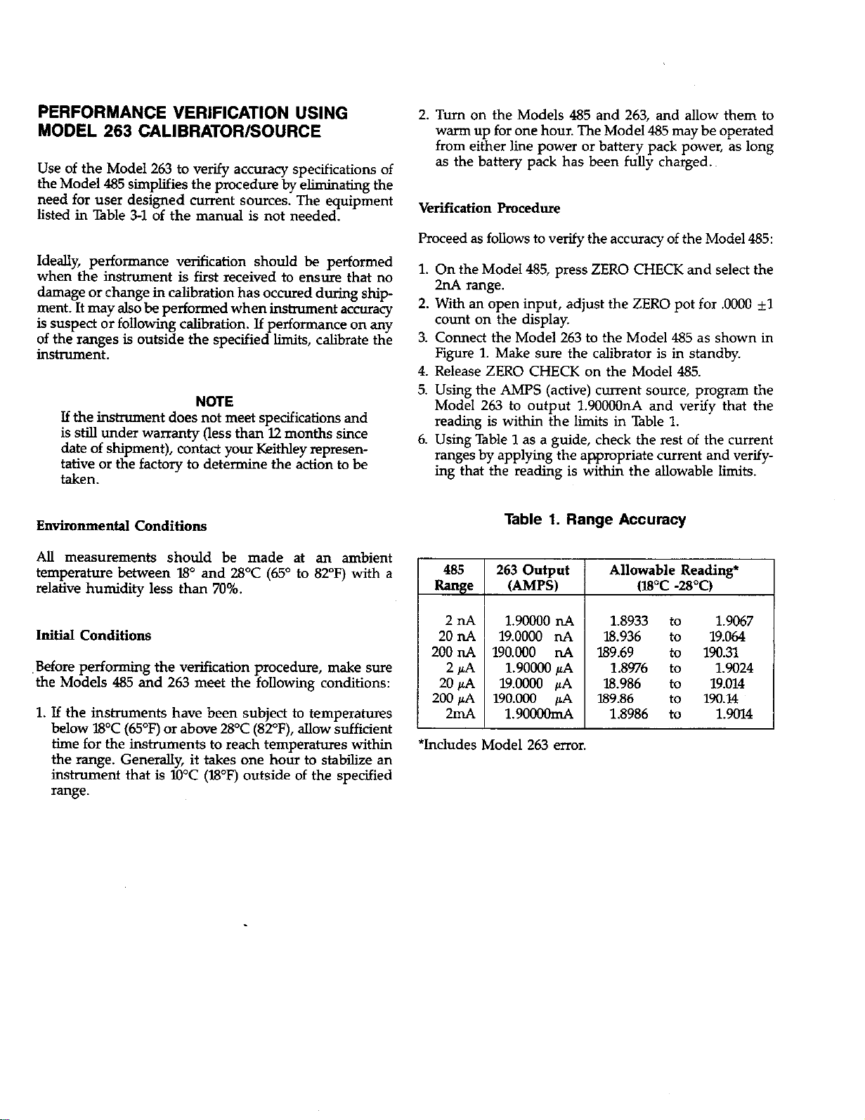
PERFORMANCE VERIFICATION USING
MODEL 263 ~LIBRATOR/SOURCE
Use of the Model 263 to verify ac~aq specifications of
the Model 485 stip~ies the prored~ by etiating the
need for user desi~ed _nt somces. The quipment
fisted h Table >1 of the manual is not needed.
Idetiy performance verification shotid be perfomed
when the tis~ent k first received to emm that no
daage or chmge h calibration has ocmed dtig ship
ment. It may&O be perfomed when fi~ent acwa~
is swpe~ Orfo~w~ c~bration. E perfmrnance on any
of the rmges ia outside the specified tits, ctibrate the
titiment.
NOTE
Mthe
~ent does not meti spedicatiom md
is stfl under warrmty ~ess thm Q months stice
date of shipment), con~d your ~lMey mpmsentative Orthe factory b detetie the atimr to &
t&en.
2. Tm on the Models 485 and 263, and allow them to
wm up for one hour. The Model ~ may be operated
from either ~ie power or battery pack power, as long
as the batteq pack has been fu~y charged..
Veficatirur Prncedw
Weed as fo~ows to verify the accuraq of the Model 485:
1. On the Model 485, press ZERO CHECK and select the
M rmge.
2. With an open input, adjust the ZERO pot for .0000 *1
cmrnt on the display.
3. Comect the Model 263 to the Model 485 as shown in
Fi~e 1. Make sue the cdlbrator is in standby.
4. Relesae ZERO CHECK on the Model 485.
5. Using the AMPS (adive) c~nt source, program the
Model 263 to output 1.90~nA and verify that the
reading is within the Itits h Table 1,
6. Using Table 1 as a guide, check the rest of the current
ranges by applying the a~ropriate current and verifying that the reatig is within the allowable limits.
Etimenti Condltiom
M measurements shodd be made at m mbient
temperature b~een M“ md 28°C (&” to 82°~ with a
relatiw humidity less thm 70°h.
Irritid
Conditimra
Before perfofig the verification procedure, m&e sure
the Models 485 md 263 meet the fo~owtig conditiom:
1 E the tis~ents have been subjed b tempmams
blow M°C (&°F) Orabom 28°C (82°F), dow sufficient
tie for the titruments to reach temperahs tithti
the rmge. GenerWy, it tskes one hour to stabtie m
irrs~ent that is M“C (MOF)outside of the specfied
range.
Table 1. Range Accumcy
263 Output
(AMPS)
1.90M0 A
19.0000 M
190.WO A
1.90000 PA
19.0000 ~A
190.000 @
1.9oooofl
*Includes Model 263 error.
Allowable Reading*
(M”C -28°C)
1.8933 to
B.936 to
M9.69 to
1.8976
28.986
to
to
E9.86 to
1.8986 to
1.9067
19.064
190.31
1.9024
19.014
lW.14
1.9014
Page 12
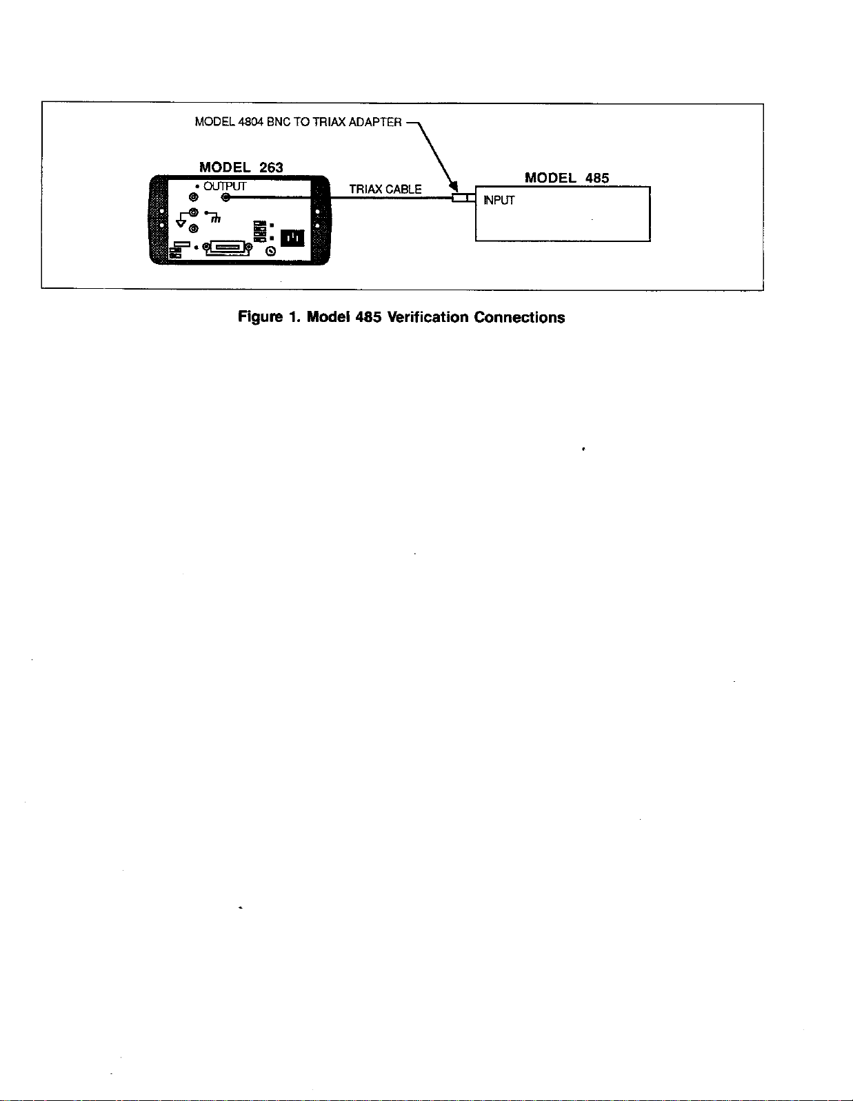
MODEL 4W BNC TO TRIW ADAPTER
MODEL 263
Rgum 1. Model 485 Verification Connections
\
MODEL 485
.
Page 13

CALIBRATION USING MODEL 263
CALIBRATOWSOURCE
me fo~oting pua~aphs ptide detded pmcedwes for
c~bratig the Model 485 Picommeter using the Model
263 Wbrator/Some. M but one of the cfibratimr adjmtienta ~e digiti md ~ & done km the ~nt pmel
m over the ~EE~ bus.
TOc~brate the tis~ent bm the tint pmel, pefiom
the fo~otig pmedures, muitig pma~aph ‘TEEE=
BW Cfibration”. TO ctibate the Model 485 over the
=4 bus, pdom the foflwtig pmedmes, ornitig
pmagaph ‘Tmnt ~el Mbration”.
Environmental Conditions
C~bration shmdd be pefiomed under labrato~ ccm&tiom hatig m -bient tempera~ of 23 +l°C md a
relative hufidity of less tha 70%. With both the Model
485 and 263 on, dow them to wam up for one hem. K
either ina~ent has ken subjected to mtieme temperatim or hufidity, dow at least one ad~tiond how for
the titiment to stabike before be@tig the ctibration procedw.
NWE
Cfibration can be stopped at ay tie md ody
those ranges out of spwificatimr need be cdbra~d.
Calibmtion Stomge Enable
The Model 485 mmt be in cfibratimr storage enable to
stem cfihation comtita h NVRAM. E the instiment
k not placed h ti mode, subsequent ctibration W be
lost when the ~
~g steps tO enable cab~mtiOn stOrage.
1. Mthe Model 485 is presently rm, * it off.
2. We holtig k the S~/CLR button, - the ina~ment back on.
3. When the “CA~ message is displayed, mle=e the
~/CLR button. The ina~ent ti ~ to the rmrmd diapl~ mode md the stotig of cdibratimr cons~ts is now enabled.
at k bd off. @fiOm the fOflw-
Required Equipment
The fo~-g item (one of each) me necess~ ti ctihate
the Model ~:
1. WitMq Model 263 Cti&ator/Some.
2. Trim to Tri= Cable (suppfied with 263)
3. kiW~ Model W Mde BNC to Pemde Tfi Adapter.
N~: The fo~owtig ad~tiond item@ be nwces~
if c~bration is to be petioned over the ~E4 bus.
4. KiMey Model 4853 EEE48 Intetiace tisti~ed h the
Model 485.
5. ~ 85 Computer eqtipped tik ~ 82937 GP~ kterface md 1/0 ROM.
6. KltMey Model 7008 ~E cable.
Front Panel Calibmtion
Petiom the foE- steps to dbrate the Model& tim
the front pmek .
1. On the Model 485, depress ZERO C~CK and select
the M rmge.
2. With m open tiput, adjust the Z~O pot for.~ AI
count on the display.
N~E
H
Q104, U105, RIU, Rl14 or RIB hwe been replaced, the pico-der may not zero. See paa&aph 5.7 h the Model& btition Manual fur
the pmcedti to bdmce the tiput amp~er.
3. Comect the output of the Model 263 ~hatur/Sowe
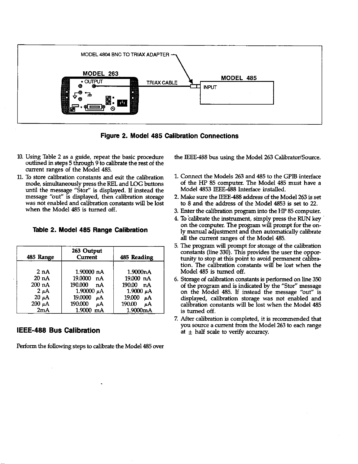
to the tiput of the Model 485 as show h Fi~ 2.
M*e sue the ctibrator is h standby.
4. On the Model 485, press the R~ arrd ~G pwhbuttmrs stidtanemrsly md hold k unti the message
“CAH is &played. Release the buttons. The tit is
now h the c~bration mode m kdicated by the “~~
annunciator.
5. Release Z~O HCK on the Model 485.
6. Pro&mn the Model 263 to output .m nA. Use the
AMPS (active) -ent some.
7. The Model& maybe displaying a smfl offset (=1
count). TOcmcel this offset, press ML rm the Model
485 to zem the display.
8. Pro~a the Model 263 to output 1.900W nA.
9. Adjust the display of the Model 485 to read l.~
uatig the S~/CLR md RCL httons. The STO/CLR
button hcrements the displayed reading and the R~
button demments the displayed reatig.
Page 14
MODEL 4W BNC TO TRl~ ADAPTER ~
MODEL 263
MODEL 485
Rgum 2. Model 485 Catibmtion Connections
10. Ustig Table 2 as a guide, repeat the basic pmcedme the ~E48 bus ustig the Model 263 C~brator/Sowe.
oufltied h steps 5 thmuxh 9 to ctibrate the rest of the
-ent range; of the M;del 485.
11. TOatom A:bration comtmta md ~t the ctibration
mode, simti~eously press the ~ md LOG buttom
UM the message “Stofl is &played. E titead the
message “ouf’ is displayed, then ctihation storage 2. Make sue the =488 adtiess of the Model 2@ is set
was not embled md cahbatimr crmstits W be lost
when the Model N is tied off.
Table 2. Model 485 Range Calibtion
263 titput
Cumnt
1.90000 d
485 Readtig
19.0000A
190.000 A
Lm &
19.0000@
190.000 @
1.9W d
IEEE-488 Bus Calibmtion
1. Comect the Models 263 md 485 to the GP~ titefiace
of the HP 85 computm. The Model 485 mti have a
Modd &53 ~488 htefiace tistied.
to 8 md the adhss of the Model 4853 is set to 22.
3. Enter the c~iration pm~m tito the HP 85 computer.
4. TO‘dbmte the titiment, stiply press the R~ key
on the computi. The -m wfl prompt for the Only marmd adjustimt md then automatically cdbrate
d the mmnt rmges of the Model 485.
5. The pm-@ prompt for storage of the c~tiation
constita me 330). ~ ptides the user the opportity to stop at this petit to avoid pemment cAha-
tiOn. me Ctibation con~ts WM ~ lost when the
Model 485 is tied off.
6. Stomge of c~bmtion comtits is pefimed mrhe 350
of the pmga md is tidcated by the “Stofl message
on the Model 485. H btead the message “out” k
displayed, c~iratiorr storage was not enabled md
c~bmtion com~ts w~ be lost when the Model &
is ~ed off,
Z After c~bration is completed, it is mcomended that
you somce a mnt fmm the Model 263 to each rmge
at k h~ scale b verify acwacy.
Pdom the fofltig steps to dbrate the Model 485 mr
Page 15
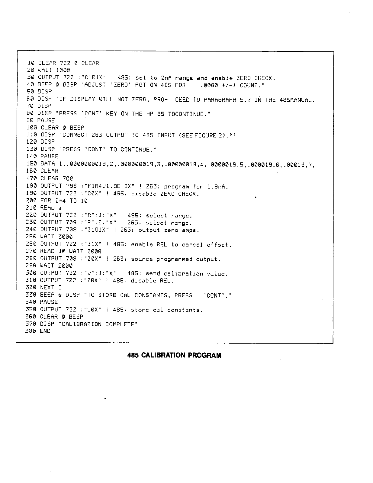
10 CLEAR 722 @ CLEfiR
NAIT 1020
22
32
OUTPUT 722 ; “CIRIX”
42 BEEP @ DISP
50 DIsP
S0 DISP “IF DISPLAY WILL NOT ZERO, PRO- CEEO TO P6RAGRAPH 5.7 IN THE 48 SMANUAL.
70 OISP
80 DISP ,’PRESS ‘CONT’ KEY ON THE HP 85 TOCONTINUE. “
90 P6USE
100 CLEAR @ BEEP
110 DISP “CONNECT ?G3 OIJTPUT TO 485 INPUT (SEE FICURE 2) ~ ~
120 DIS?
130 OISP “PRESS ‘CONT’ TO CONTINUE. “
140 PAUSE
152 06Th 1, .0000000019,2,.000000019,3, .00000019,4, .0000019,5,.000019,6, .00019,7,
160 CLEAR
170 CLEAR 708
180 OUTPUT 708 ; “F1R4UI . gE-gx,
190 OUTPUT 722 ; “COX,,
200 FOR 1=4 TO 10
210 REAO J
~ZO OUTPUT 722 ~ ,,R,, ;J; ,,x, ! 485; ~e~ect ~ange,
230 OUTPUT 708 ; R; I; ,X< ! 265; select range.
240 OUTPUT 708 ; “Z101X” ! 263; output zero amp5.
2S0 WAIT 3000
260 OUTPUT 722 ; “ZIXS’ ! 485; enable REL to
270 REAO J@ WAIT 2000
~sO OUTp UT 708 ; ,,zOx,, ! ~E~;
290 Wfl IT 2000
300 OUTPUT 722 ; “V’’; J; “X,” ! 485; send calibration value.
310 OUTPUT 722 ; “ZOX” ! 485; disable REL.
320 NEXT I
330 BEEP @ OISP “TO STORE C6L CONSTANTS, PRESS ‘CONT’ . “
340 PAUSE
‘AOJUST ‘ZERO’ POT ON 495 FOR
! 485; set to 2nA range and enable ZERO CHECK.
.0000 +/-1 COUNT. “
! 263; program for 1.9nA.
! 4S5; disable ZERO CHECK.
cancel Of
source programmed outpu
5et .
350 OUTPUT 722 ; ‘“LOX,’ ! 485; store cal constants.
560 CLEhR @ BEEP
370 DISP “CfiLIBRATION COMPLETE”
380 END
485 CALIBRATION PROGRAM
Page 16
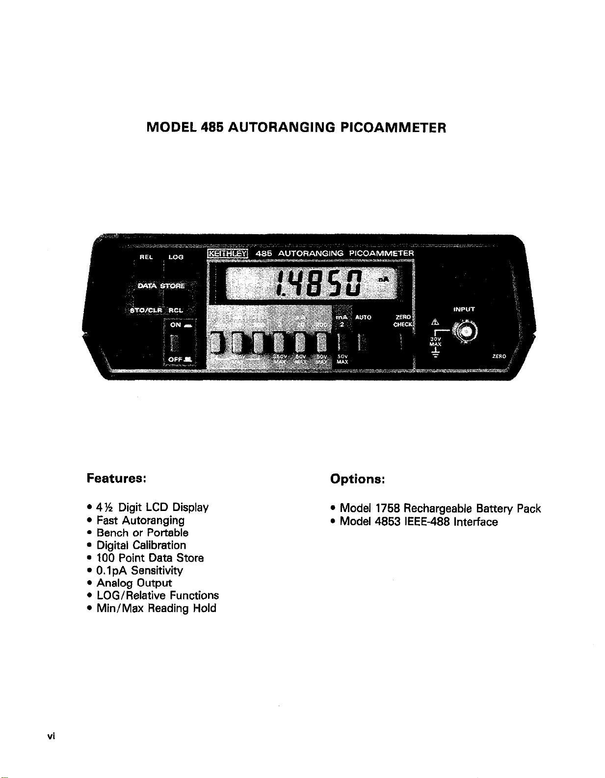
MODEL 485 AUTORANGING PICOAMMETER
vi
Features:
l 4% Digit LCD Display
l Fast Autoranging
l Bench or Portable
l Digital Calibration
l 100 Point Data Store
l O.lpA Sensitivity
l Analog Output
l LOG/Relative Functions
l Min/Max Reading Hold
Options:
l Model 1758 Rechargeable Battery Pack
l Model 4853 IEEE-488 Interface
Page 17
SECTION 1
GENERAL INFORMATION
1.1 INTRODUCTION
This instruction manual contains the necessary information
for operating and maintaining the Model 485 Autoranging
Picoammeter and the Model 1758 Rechargeable Battery
Pack. The information is divided into the following sections:
1. Section 1 contains general information and provides
guidelines for using this manual. Important safety information is also presented here.
2. Section 2 contains detailed operation information for the
Model 485.
3. Section 3 contains the information needed to verify the
accuracy of the Model 485. Performance verification can
be done upon receipt of the unit or whenever the basic accuracy is in question.
4. For the more technically oriented, information on theory
of operation, maintenance and servicing is contained in
Section 4 through 6.
NOTE
The Model 4853 IEEE-488 interface comes supplied with its own instruction manual.
1.2 GElTlNG STARTED
Perform the following steps in sequence to acquaint yourself
quickly and safely with the basic operation of the Model 485.
1.
Verify that the Model 485 was not damaged in transit, as
explained in paragraph 1.3.
2.
Carefully read the safety precautions and warnings found
preceding this section and the first two sections (General
Information and Bench Operation) of this manual.
Referring to paragraph 2.2.1 (Line Power) set the line
3.
voltage switch and plug the power cord into a properly
grounded cutlet. If the optional battery pack is installed
the charge circuitry will be activated.
4.
Acquaint yourself with the controls and display of the
Model 485 as follows:
A. Turn on the Model 485 by pressing in the ON/OFF
pushbutton. All the zeroes will be displayed briefly.
B. Select autoranging by pressing in the AUTO pushbut-
ton. The nA and AUTO annunciators will be displayed.
Pressing any of the other range pushbuttons will put
the Model 485 in manual ranging as indicated by the
absence of the AUTO annunicator.
C. Engage the ZERO CHECK pushbutton and note that
the ZERO CHECK annunciator turns on. Release the
ZERO CHECK button.
D. Select LOG by pressing the LOG pushbutton. The
LOG annunciator will turn on. Press the LOG button
again to take the Model 485 cut of the LOG measurement mode.
E. REL (relative) can be used in the linear measurement
mode or the logarithm measurement mode. The
stored REL level will be subtracted from all subsequent
measurements. Press the REL pushbutton and note
that the REL annunciator turns on.
F. To activate the 100 point DATA STORE with
MinIMax, press end hold in the STO/CLR pushbut-
ton. When the reading rate r = 0 is displayed let go of
the button. The ST0 annunciator will turn on. Press
the RCL pushbutton and the last data point will be
displayed briefly followed by the reading (data). Other
date points can be displayed by holding in the RCL
button. Turn off the DATA STORE by pressing the
STO/CLR pushbutton again.
5. When you are comfortable with the controls of the Model
485, go on and make the desired measurements using
Section 2, Bench Operation as a guide.
1.3 INSPECTION
The Model 485 Bench Picoammeter was carefully inspected,
both mechanically and electrically, before shipment. Upon
receiving the Model 485, check for any obvious signs of
physical damage that might have occurred during shipment.
Report the damage to the shipping agent immediately. Retain
the original packing materials in case reshipment becomes
necessary. The following items are included with every Model
485 order:
l Model 485 Autoranging Picoammeter
l Model 485 Instruction Manual
l Additional accessories as ordered.
If an additional instruction manual is required, order then
manual package (Keithley Part Number 486-901-00). The
manual package includes an instruction manual and all pertinent addenda.
1.4 SPECIFICATIONS
Detailed Model 485 specifications may be found immediately
preceding the table of contents of this manual.
1.5 WARRANTY INFORMATION
Warranty information may be found on the inside back cover
of this manual. Should it be necessary to exercise the warran-
ty, contact your Keithley representative or the factory to
determine the correct course of action. Keithley Instruments
maintains service facilities in the United States, West Germany, Great Britain, France, the Netherlands, Switzerland
1-l
Page 18

and Austria. Information concerning the application, cperaticn or service of your instrument may be directed fc the ap-
plications engineer at any of these locations. Check the inside
front cover of this manual for addresses.
Model 1684 Hard Shell Carrying Case-Hard vinyl case,
IOOmm x 300mm x 350mm (4 x 13 x 14 inches) has a fit-
ted foam insert with room for the Model 485, instruction
manual end small accessories.
1.6 MANUAL ADDENDA
Information concerning improvements or changes to the in-
strument which occur after the printing of this manual will be
found on an addendum sheet included with this manual. Be
sure to review these changes before attempting to operate or
service the instrument.
1.7 SAFETY SYMBOLS AND TERMS
The following safety symbols and terms are used in this
manual or found on the Model 485.
The symbol
should refer to the operating instructions in this manual.
The WARNING heading in this manuel explains dangers that
could result in personal injury or death.
The CAUTION heading in this manual explains hazards that
could damage the instrument.
1.8 OPTIONAL ACCESSORIES
The following accessories can be used with the Model 485.
Model 1010 Single Reck Mounting Kit-Use to mount
one Model 485 in e standard 5% x 19” rack.
on the instrument indicates that the user
A
Model 1768 Rechargaable Battery Pack-Provides six
hours minimum operation from full charge, recharges within
10 hours end is field installable.
Model 4801 Input Cable-A low noise coaxial cable four
feet (1.2m) in length with a male BNC connector on each
end.
Model 4803 Low Noise Cable Kit-Consists of 50 feet
(15.2m) of low noise coaxial cable, 10 male BNC connectors,
and five female chassis mount BNC connectors.
Model 4863 IEEE-486 Interface-Field installable prcgram-
mable option provides isolated data output. Switchselectable talk only or addressable modes. Mounts within and
powered by the Model 485.
Model 7008 IEEE-488 Digital Cable-Useful for ccnnecting the Model 4853 to the IEEE-488 bus. The Model 7008-3 is
0.9m 13 ft) in length and has a standard IEEE-488 connector
at each end. The Model 7008-6 is 1.8m (6 ft) in length.
Modal 8673 IEEE-486 Interface for IBM PC-Field in-
stallable programmable option provides data output for the
IBM PC. Mounts within and powered by the IBM PC.
Model 1017 Dual Reck Mounting Kit-Use to mount two
Model 486’s in a standard 5% x 18” rack.
l-2
Page 19

SECTION 2
BENCH OPERATION
2.1 INTRODUCTION
This section contains the information needed to prepare and
operate the Model 485 as a bench picoammeter. Bench
operation consists of using the Model 485 to perform basic
current measurements. Data store operation is also covered.
The capabilities of the Model 485 can be enhanced with the
addition of the Model 4853 IEEE-488 interface. IEEE operstion is covered in the Model 4853 Instruction Manual.
2.2 PREPARATION FOR USE
2.2.1 Line Power
The Model 485 is provided with a three-wire line cord which
mates with third-wire grounded receptacles. Connect the in-
strument to AC line power as follows:
1. Set the LINE VOLTAGE switch on the back of the instrument to correspond to line voltage available. Ranges are
105-125V or 210-250V 50/60Hz AC.
CAUTION
Connect only to the line voltage selected.
Application of incorrect voltage can
damage the instrument.
2. Plug the power cord into a properly grounded outlet.
WARNING
Ground the instrument through a properly
grounded receptacle before operation.
Failure to ground the instrument can result
in severe injury or death in the event of
short circuit or malfunction.
NOTE
Although the Model 485 is specified at 50Hz and
60Hz the instrument may be operated at 400Hz
and 440Hz. Add one count to instrument
specifications under this condition.
2.2.3 Battery Charging
After the Model 1758 Banery Pack is installed in the Model
485 it can be charged and recharged as follows:
1. Connect the instrument to line power as described in
paragraph 2.2.1.
2. With the power switch off, the battery charge circuitry is
automatically energized to charge the battery at the maximum rate. When the battery pack is first installed, or if it is
completely discharged, allow it to charge for ten hours.
NOTE
For maximum battery efficiency only charge the
battery pack after it has become discharged and
only charge until it is fully charged I,10 hours).
Continuous charging over long periods of time
will not damage the batteries but, useful life will
gradually decrease. This loss is not permanent
and may be restored by cycling the battery pack
through several complete charge/discharge
cycles. The battery pack is capable of 500 to
1000 charge/discharge cycles before replace-
ment is needed.
Do not make measurements with the BAT annunciator on as
the readings may be erroneous.
3. When the Model 485 is in use on line power, the banely
charger maintains a trickle charge on the battery pack.
2.3 TILT BAIL
The Model 485 is equipped with a tilt bail which makes it
possible to elevate the instrument to a convenient viewing
position. To change the bail position, pull out the bail handle
from each side of the case until it rotates freely; rotate the bail
to the desired position and release the bail to allow it to lock
into place.
2.4 MODEL 485 FAMILIARIZATION
2.2.2 Battery Pack Power
The Model 485 may also be operated from rechargeable
sealed nickel-cadmium batteries contained in the optional
Model 1758 Rechargeable Battery Pack. The battery pack will
operate the Model 485 for up to six hours. The BAT ennunciator will turn on when the banely charge is insufficient to
maintain eccurate readings. Refer to Section 5, paragraph 5.3
for installation procedures.
The following paragraphs and Figure 2-l provides a brief
description of the display, front panel controls and connec-
tors.
2.4.1 Display
The Model 485 has a 4% digit liquid crystal display (LCD).
The minus sign is displayed. The plus sign is implied by the
absence of the minus sign. The following annunciators are
displayed on the LCD.
2-l
Page 20

BAT-Low battery indicator for the Model 1758.
nA. uA or mA-Nanoamos. Microamos or Milliamos
selected.
RMT IRemote)-Model 485 being controlled over the
IEEE-488 bus (Model 4853 installed).
CAL-Model 485 in calibration mode.
AUTO-Autorange selected.
REL-Relative selected.
LOG-Logarithm selected.
ZERO CHECK-Zero Check selected.
BTO- Data being stored.
RCL-Data being recalled. RCL flashes when buffer is full
during store cycle.
1. STO/CLR-Pressing this button initiates the storage sequence. Pressing the button a second time shuts off the
data store when in r=Othrough r=5. When in r=6, pressing this button stores one reading.
2. RCL-Pressing and holding this button in scrolls the data
pointer. To read the data at a particular point, simply
release the button.
Range Pushbuttons
1. Auto-This pushbutton selects autoranging.
2. Manual ranging is accomplished by depressing the appropriate range button.
2.4.2 Front Panel Controls
ON/OFF-Pressing in this pushbutton turns the Model 485
on. Releasing (out) this pushbutton turns the instrument off.
ZERO CHECK and ZERO-This pushbutton and trimpot are
used to zero the instrument’s internal offsets.
REL (Relative)-This pushbutton is used to cancel measurement offsets or store the input signal as a reference level.
Pressing this button again shuts REL off.
LOG-This pushbutton selects the logarithm function. The
displayed current measurement is expressed as the logarithm
(base IO) of the measured current referenced to one ampere.
Pressing this button again shuts LOG off.
DATA STORE-Has MlNlMAX and 100 point reading
storage capachY; records data at one of seven selectable
rates. Records minimum and maximum conversion during
the period the data store is active at the rate of 3/set.
ITHLEY 485 AUTORANGING PICOAMMETER
i_J
2.4.3 Input Connector
The input connector is a standard BNC type.
2.4.4 Analog Output Connectors
A voltage level that is proportional to the incoming current
can be monitored using the analog output banana jacks
located on the rear panel.
2.5 ERROR MESSAGES
Table 2-1 lists the error messages associated with basic front
panel operation. Note that the instrument has a number of
other messages that are discussed in the appropriate sections
of this manual.
4 \
2-2
Figure 2-l. Model 485 Front Panel
Page 21

Table 2-l. Error Messages
Display Message Comments
im RAM Error
IpEz
kiir-
2.6 ENVIRONMENTAL CONDITIONS
All measurements should be made at an ambient temperature
within the range of O°C to 50°C, and with a relative humidity
of 0% to 70% up to 35OC. For instruments above 35OC
derate humidity 3% per OC up to 50°C. If the instrument has
been subjected to extremes of temperature, allow sufficient
time for internal temperatures to reach environmental condi-
tions. Typically, it takes one hour to stabilize a unit that is
10°C IlEaF) out of specified temperature range.
2.7 BASIC BENCH MEASUREMENTS
Basic measurement techniques for using the Model 485 to
measure DC current are covered in the following paragraphs.
Also included is the operation of the MinIMax and 100 point
data store. A summary of range, accuracy and maximum
allowable input information is given in Table 2-2.
Calibration Error Model 485 locks up, but operation can be restored by pressing
INVRAM Failure) any one of the four momentary pushbuttons. If restored, calibration
Overrange Overrange input applied to the Model 485. Leading minus sign
Model 485 locks up. See Section 5 for troubleshooting information.
is invalid as indicated by the flashing “CAL” annunciator. See Sec-
tion 5 for troubleshooting information.
indicates that input signal has a negative value.
WARNING
Before operating the Model 485, observe
the safety precautions found preceding
Section 1. Failure to observe these and
other safety precautions found in this
manual could result in severe injury or
death.
WARNING
Do not exceed 30V RMS between input low
and power line ground or a shock hazard
will result. Also, current inputs that exceed
3mA may be erroneously displayed as a”
on-scale reading.
CAUTION
Do not exceed the maximum input limits
shown in Table 2-2.
Table 2-2. Range, Accuracy and Maximum Allowable Inputs
r
Maximum Accuracy Source
Flli;lry i *l%Reading + Counts1
Range
2mA
1.9999 nA
19.999 nA
199.99 nA
1.9999 pA
19.999 pA 0.1 + 1
199.99 pA 0.1 +1
1.9998mA
2 nA
20 nA
200 nA
22$
200 PA
IOTE:
Current above maximum will result in an “OL” display.
,. Source resistances lower than these may result in higher instrument noise and drift.
i. Maximum Transient Overload Voltage: IOOOV with a series 1OOkB resistor. Safe
operation and good measurement practice dictates use of an external resistor when
necessary to limit input currents to less than 3mA.
Maximum volts-hertz product (common mode): 108V.H~
lB°C -28OC (Note 2) (Note 3)
0.4 + 4
0.4 + 1
0.2 + 1
0.15 + 1
0.1 +1
Minimum
Recommended Maximun
Allowablt
Resistance
1OOMB 350v
1OOMB 350v
10MB 350v
1MB 350v
100 kC 5ov
10 kB 5ov
1 kKl 5ov
Input
1
1
2-3
Page 22

2.7.1 Power-Up
NOTE
The software revision level of the Model 485 can
be disolaved uoon oower-uo bv runnino the
diagnostic program. See .Section 5,
Maintenance, for more information.
Turn on the Model 485 by pressing in the ON/OFF switch.
The following will occur automatically:
1. Reset- All zeroes will be briefly displayed before going into
the measurement mode.
2. RAM Test-If this test fails the Model 485 will lock up with
zeroes displayed.
3. NVRAM Test-This test determines if the calibration constants are properly read from NVRAM. If this test fails the
display will show the error message “cErr”.
Refer to Table 2-1 for more information pertaining to error
messages.
CAUTION
During power up and power down, using
AC line or battery pack, a current surge
15mA, 5V maximum) can appear at the INPUT of the Modal 455. Protect any circuitry
that would be damaged by these levels by
making circuit connections only after turning on the Model 485. Disconnect these circuits before turning off the Model 485.
2.7.2 Zero Check
The instrument should be properly zeroed (after one hour
warm-up) before making any current measurements. Only
the 2nA current range needs to be zeroed. To check or adjust
zero, proceed as follows:
1. Select the 2nA range.
2. Turn off REL and LOG if they are on.
3. Depress the ZERO CHECK pushbutton. Momentary or
locking action can be achieved depending on how far the
button is depressed. To adjust zero, place the pushbutton
in to the lock position.
4. Adjust zero level trimpot via access hole on front panel for
a zero indication on the digital display.
5. Release the ZERO CHECK button.
In normal operation, the equivalent input resistance of the
485 picoammeter is equal to or less than the maximum
burden voltage (2OOfiV) divided by the maximum range current. This does not hold while in zero check or overload con-
ditions because the feedback to the input node is broken.
Values of input impedance for normal operation and zero
check/overload are shown in Table 23.
NOTES
1. When zero is properly adjusted, the input voltage burden
for an on-range reading will be less than or equal to 2OOpV.
2. The REL feature can be used instead of the ZERO pot to
zero the display. However, REL then cannot be used to
cancel a measurement offset or establish a reference level.
Table 2-3. Equivalent Input Resistance With Zero
Check Enabled
:urrent Maximum Effective Impedance In
Range
2 nA 1OOkD 9MGll230pF
20 nA
200 nA
2::: 100 10 D a 900k08230pF 100kGll0.01~F
200 pA lOkDUO.OlpF
2mA 0.: IY Ik9ljO.Ol~F
2.7.3 Current Measurements
1. Zero the instrument as described in paragraph 2.7.2.
2. Select a current range that is appropriate for the expected
input level or select autorange.
3. Connect the source to the INPUT connector on the front
panel. Low-noise cable and connector accessories de-~
scribed in Section 1 should be used as required. Measurement considerations are discussed in paragraph 2.8. A
summary of range, accuracy and input overload information is given in Table 2-2.
4. Read the input current on the digital display. Overrange is
indicated by an “OL” message.
2.7.4 Relative Mode
When the relative mode is selected with an on-scale reading
on the display the following occurs:
1. The REL annunciator is displayed.
2. The next reading is stored.
3. The stored reading is then algebraically subtracted from all
subsequent readings and displayed.
A REL level can be established for the linear measurement
mode or the logarithm measurement mode and is effective
only in that mode. Changing modes will not affect a REL level
already established. However, if another REL level is set fin
the other measurement mode) the previous REL level will be
cancelled. For example, place the Model 485 in the logarithm
mode (LOG annunciator on) and select the 2pA range. With
an open input, note the approximate -10.0 reading on the
display. Press the REL button and note that the REL annunciator is on and that display is zeroed. Select the linear
measurement mode by pressing the LOG button (LOG annunciator off). Note that the REL annunciator is off, indicating that there is not a REL level established for the linear
measurement mode. Switch back to the LOG mode and note
Input Resistance Zero Check/Overload
IOkD 9MDjj230pF
IkD 5MCll230pF
2-4
Page 23

that the REL level is still there. Again, go back to the linear
measurement mode (LOG off) and set a REL level of lfi. the
REL annunciator will turn on. Switch back to the LOG mode
and note that the REL annunciator is off, indicating that the
REL level for the LOG mode is cancelled.
Once a REL level is established for a measurement mode, that
stored level will be the same regardless of what range the
Model 485 is on. For example, if + IMA is established es the
AEL level on the 20/~A range, + IpA will also be the REL level
on the 2mA range.
It is important to note that the use of REL reduces the
dynamic range of measurements by that level. For instance,
assume that the REL level is + IpA and the Model 485 is
manually set to the 26 range. The maximum positive
displayed reading (before overranging), would be
+0.9999& This is because the A/D converter would be
seeing 1.9999fl (maximum) from the input. Thus, the
dynamic range of measurement is -1.9999fi to +0.9999fi
(2.9998fi) as compared to the normal -1.9999fi to
+ I .9999/rA (3.9998$1. The dynamic range of measurement
has been reduced by l& The effects on dynamic range can
be reduced by selecting a higher range or using autorange.
2.7.6 LOG Mode
The Model 485 can make logarithm measurements refer-
enced to a 1A current level or to other current levels with the
use of the REL feature.
The following examples compute the expected LOG
readings for various current levels applied to the Model
485:
A. InA
LOG reading = LDG +$LOG reading = -9.000
B. 0.5&A
LOG reading = LOG LOG reading = -6.301
C. -1mA
LOG reading = LOG I+1
LOG reading = -3.000
To make LOG measurements reference to lA, proceed as
follows:
A. Zero the instrument, if required, as described in
paragraph 2.7.2.
B. Select auto range on the Model 486.
C. Connect the source to the Model 485.
D. Press the LOG button.
E. Take the LOG reading from the display.
2. Log measurements using other reference currents:
LOG measurements, referenced to other current levels,
can be read directly from the display of the Model 485 by
utilizing the REL feature and an accurate current source.
I I
0.5fi
I I
The basic procedure for using the LOG mode is to select auto
range and press the LOG button (LOG annunciator on). To
get out of the LOG mode, press the LOG button again. The
LOG annunciator will turn off.
Because the logarithm of a negative number is undefined, the
logarithm is taken with the absolute value of the measured
current.
NOTE
LOG measurements must always be made on
the lowest Dossible ranae (without overranging).
Readings dn high ranges will not allow Optimum
calculations of the logarithm. When in doubt,
use Auto Range.
1. Log Measurements with IA reference currant: The
LOG measurement mode displays the absolute value of
the logarithm (base 101 of the input current referenced to
IA. The following equation illustrates this relationship:
LOG Reading = Log
Using this reference &rent, the LOG riading span is from
-13.0 (fO.lpA) to -2.699 (1tI.9999mAl.
Applied Current
I
IA
To make LOG measurements referenced to another cur-
rent level, proceed as follows:
A. Z.&o the instrument, if required, as described in
paragraph 2.7.2.
B. Set the Model 485 to auto range.
C. Input the reference current to the Model 485.
D. With the Model 485 in the LOG mode, press the REL
button. The REL annunciator will turn on and the
display will zero.
E. Remove the reference current source from the Model
485.
F. The Model 485 is now set up to make LOG
measurements referenced to that current level. Simply
input the current to be measured and take the reading
from the display.
2.7.6 Inverting Analog Output
Two banana jacks, accessible from the rear panel, permit
monitoring or recording of the output from the current-to-
voltage converter within the Model 485. Since the Model 465
is a feedback picoammeter, as shown in Figure 2-2, the input
current is forced through the feedback resistor and an in-
2-5
Page 24

verted analog output voltage is developed by the operational
amplifier. The feedback (Rangel resistors are selected such
that voltage for an on-scale reading on the 2nA range will be
between zero and k200mV. The output voltage for the rest
of the ranges will be between zero and f2V. The relationship
between the analog output signal and the digital display is as
follows:
2nA Range: 10000 counts = -1OOmV. or -1OFVIcount
20nA-2mA Ranges: 10000 counts = -IV or -lOO~V/count
The analog ouput is input protected up to 20V RMS and during an input current overload the analog output is clamped to
a maximum voltage swing of approximately *4V. Although
protected up to 20V to prevent instrument damage, a voltage
applied to the analog output could cause an erroneous
display, rather than the “OL” message.
Since the output of the current-to-voltage converter is
bipolar, the inverting analog output can also be used to
measure low frequency AC current which falls within the
specified analog rise time. The inverting analog output
resistance is 1 .Ol kD; 9lOD in series with the signal leads and
1OOD in series with the ground lead.
Typical Analog Output Accuracy:
Linearity: < 0.1% full scsle
Gain Accuracy: k 1%
Output Resistance: +5%
Ff+ ‘Efif
Figure 2-2. Model 485 Inverting Analog Output
2.7.7 Mm/Max and 100 Point Data Store
The data store can save up to 100 readings and store the
minimum and maximum readings recorded during the period
that the data store is active. The 100 points of data are stored
at one of six selectable rates. Manuel data entry (r = 6) is also
available. Readings for minimum and maximum are sampled
at the rate of three per second regardless of the selected rate.
The minimum and maximum readings are continuously updated while in the data store mode. The procedure for
operating the data store is as follows:
1. Connect the desired measurement configuration to the
Model 465. Make sure that the controls of the Model 485
are set appropriately.
2. Storing Data:
A. Press and hold the STO/CLR pushbutton. The follow-
ing reading rates will scroll on the display:
r = 0 I3 rds/sec)
r = 1 (1 rdglsecl
r = 2 (1 rdg/lO secj
r = 3 II rdglmin)
r = 4 (I rdg/lO mini
r = 5 (I rdglhr)
r = 6 (I rdg every time ST0 button is pressed)
NOTE
There is no need to select a rate if just
minimum/maximum readings are desired.
Momentarily press the STO/CLR button to start
the store.
6. Release the STO/CLR pushbutton when the desired
reading rate is displayed. The ST0 annunciator will
turn on and data will be stored at the selected rate.
NOTE
The date store cycle can be terminated at any
time by doing the following:
A. If in r=6 mode, press the RCL button and
the STO/CLR button.
6. If in any other r mode, only press the STO/
CLR button.
With the data store off, data is retained and can be recalled at
any time as long as the instrument remains on.
3. Data Retrieval: Data can be retrieved at any time, but a
flashing RCL annunciator indicates that the maximum
number of readings (100) have been stored.
A. Press and hold in the RCL pushbutton. The display will
scroll through the date points and MlNlMAX (LO/HI).
The first data point displayed will be the last stored
reading. The next two data points will be the HI and LO
readings made during that store cycle. Notice that the
longer the RCL pushbutton is held in the faster the data
points will scroll on the display.
B. Release the RCL pushbutton at the desired data point
and note the reading (data) on the display. The data
pointer can be incremented by steps of one by momentarily holding in the RCL pushbutton.
4. Shut off the data store by pressing the STO/CLR
pushbutton. All stored data will be retained until a new
store cycle has commenced.
2.6 MEASUREMENT CONSIDERATIONS
This section describes the effects of source resistance,
capacitance, noise and leakage resistance on the measurement. Other measurement considerations are also discussed.
Minimum and maximum values of these source parameters
are defined, at which point a significant degradation of the
measurement can begin to occur. Compensation methods
are described to minimize these effects. Refer to Figure 2-3
for the following discussion.
2-6
Page 25

2.8.1 Source Resistance
Increasing capacitance beyond this level may increase noise
and induce instrument instability. The noise gain of the
As shown in Table 2-2, a minimum value of source resistance
is recommended for each range. The reason for this can be
understood by examining Figure 2-3. Considering effects on
low frequency noise and drift, CS and CFB can momentarily
measurement circuit can be found from:
Equation 2.
Output en = Input en x(1 +
be ignored. where ZF =
Input amplifier noise and drift appearing at the output can be
calculated as follows:
Equation 1.
Output enOiSe = IflpUt enOjSe
x(1+ -@)
Thus it is clear than as long as RS>>RFB, Output enoNe fz
Input enoNe. When RFB = RS, Output enojse = 2 x input
enoise,
The same applies for eos.
, , cFB
CS
II
I I
RFB
(1 Es
RS
Slrm
WVV
lOon
T--
ANALOG 10,OOOpF is leakage measurement of capacitors. In this case
OUTPUT
.
TO A/D
CONVERTER
v
6
Figure 2-3. Simplified Model for Input Signal
Conditioning
RFB
\j
and ZS =
RS
42a fRSCSP+ 1 j
Clearly ss f -0
equation (2) reduces to equation (I).
The frequency range in interest is O.lHz to IOHz which is the
noise bandwidth of the AID convener. The value of CF is
22OpF for nA ranges and O.OlpF otherwise.
In general, as CS becomes larger, the noise gain becomes
larger. An application where CS may be greater than
Input en must include the effects of the voltage source (ES)
used to bias the capacitor. The Keithley Model 230 is recommended for this application.
When measuring leakage currents on capacitors larger than
10,OOOpF. stability and noise performance can be maintained
by adding a resistor in series with the capacitor under test.
The value of this resistor shoulde be around 1 MB. For large
capacitor values (z lrFj, the value of the series limiting
resistor can be made lower in order to improve settling times:
however, values below 1OkD are not generally recommended.
Model 485 will typically show insignificant degradation in
displayed performance with the noise gain of 2 resulting from
allowing RS = RFB. Typical amplifier input enOjSe is about
5@ p-p in a bandwidth of 0.1.IOHz. Amplifier ECS can be
nulled with front panel ZERO adjustment, but available
resolution limits this adjustment to about 5V. The
temperature coefficient of ECS is < 2OpV/“C. These
numbers can be used with Equation 111 to determine ex-
pected displayed noise/drift given any source resistance.
Remember that 1 displayed count = lOO$/ except on 2nA
range where 1 displayed count = lO@V. Note also that the
values given in Table 2-2 for minimum source resistance also
represent the value of RFB on that range.
2.8.2 Source Capacitance
The Model 485 is designed to accomodate up to 10,OOOpF in-
put capacitance ICS). This limit will preclude problems in
most test setups and allow extremely long input cable lengths
without inducing instabiliw or oscillations.
This resistor is not critical in terms of tolerance or stability.
Any carbon composition resistor will prove adequate.
A second-order advantage to using this limiting resistor is sdded protection to Model 485 in the event of capacitor failure.
2.8.3 Leakage Resistance
The effect of leakage currents should be considered when
making small current measurements with high impedance
sources. Leakage current and its effects can be minimized by
using high resistance insulation in the test circuits and guerding. Since the Model 485 is a feedback picoammeter, it is ef-
fectively guarded at the input. The effect of leakage paths on
the measurement can be further minimized by using a gusrd-
ed text fixture as shown in Figure 2-4. In the configuration
shown, the current through the component under test will
not be shunted significantly by either leakage resistance path.
If a high voltage supply is used to make high resistance
leakage measurements, it is suggested that a series current
2-7
Page 26

limiting resistor be used to prevent exceeding the maximum
overload input limit of the Model 455 in the event the item
under test is shorted.
2.5.4 Zero Time Stability
The typical zero time stability of the Model 455 is less than
one count per week, exclusive of temperature effects.
SHORT
CIRCUIT
CURRENT -
LIMITER
TEFLON
INSULATOR
VVV’I
Figure 2-4. Test Fixture Guarding
2.5.5 Grounding Considerations
Input LO (outer ring of input connector) should be connected
to a potential at the source which is within 30V RMS of
power line ground of the Model 455 or the equipment near it.
Connection to power line ground is not made internally in
order to avoid possible ground loops.
MODEL 485
2.5 APPLICATIONS
The following applications can be automated to various
degrees with the use of programmable equipment over the
IEEE-455 bus. The Model 455 becomes fully programmable
with the addition of the Model 4553 interface. Programmable
sources are available from Keithley and other manufacturers.
The documentation that is provided with the Model 4553 includes example programs using various controllers.
The Model 455 may be used in conjunction with the Model
6104. The Model 6104 is a guarded and shielded test box for
2-terminal or 3-terminal connections. The Model 6104 pro-
vides excellent electrostatic shielding and high isolation
resistance for the component under test. Clips plug into
banana jacks allowing the user to fashion modified connec-
tions to suit the component to be tested.
The Model 6104 is useable with the Model 455 picoammeter
and Keithley voltage supplies, such as the Model 230. When
connected together as a system, using the cable and connector options, they form a complete test facility for measuring
leakage current and other low current parameters for various
test applications. A possible test set up is hewn in Figure 2-5.
The measurement sample would be connected between Jl
and J7 or J6.
EXT. SOURCE
MODEL
BLhK [ j4 45 j
CASE
Figure 2-5. Leakage Test Sat Up Using Modal 6104
2.9.1 Op Amp Input Offset Currents
As the parameters of new BIFET, BIMOS, and FET op amps
approach the parameters of the ideal op amp, such
characteristics as the input offset current are breaking
through the 1pA level. Use the Model 455 to measure these
low level currents as shown in Figure 2-6. Note the connection of Model 455 input low.
2-5
Figure 2-6. OP Amp Input Offset Currents
Measurement
Page 27

2.9.2 FET Gate Leakage and Channel Currants
Analog switches, multiplexer circuits, sample and hold circuits, integrators, LED drives, and many other circuits have
errors generated by either gate leakage or channel leakage in
FET-based components. For understanding the design limita-
tions of a component or for tight component selection use
the Model 485 as shown in Figure 2-7.
Figure 2-7. FET Gate Leakage and Channel Currents
Measurement
2.9.3 Insulation Leakage Currents and High Resistance
In precise low power, low current circuitry, stray leakage cur-
rents can adversely affect circuit performance. Since leakage
current is a non-linear function of voltage, the expected
voltage level must be applied.
Leakage resistance of 10% can be determined with the
Model 485 and a voltage source of 1OOV. Using this tech-
nique, you can evaluate high resistance materials or insulation leakage of capacitors, PC boards, switches, or connectors under normal environmental conditions and under
elevated temperature and humidity conditions. (see Figure
Z-8).
Figure 2-S. Insulation Leakage Currents and High Resis-
tances Measurements
2.9.4 Phototube. Photodiode and Beam Currents
Photomultiplier tubes and other light detection devices require precise measurement of a wide range of currents (see
Figure 2-9). Beam currents used for ion implantation, surface
phenomena studies, and atomic structure analysis using
scanning electron microscopy are in the picoamp to nanoamp
range. The Model 485 has the accuracy and sensitivity to
make these measurements with routine ease. In addition, for
these applications it is convenient to cancel out dark currents,
using the Model 485’s “REL” feature. To present data in a
logarithm format, simply touch the “LOG” button. Use the
AUTO ranging feature to cover a broad dynamic range.
SCANNING
ELECTRON
MICROSCOPE
Figure 2-9. Setup to Measure Photomultiplier, Photodiode and Beam Currents
2-9
Page 28

2.9.5 Resistivity Tests
The Model 485 may be used along with the Model 6105 to
perform resistivity tests. The Model 6105 is a guarded test fix-
ture for measurement of surface and volume resistivities. The
chamber is designed in accordance with ASTM Standard
Method of Test Electrical Resistance of Insulating Materials,
D257-66. The Model 6105 can be used in conjunction with
the Model 485 and a high voltage power supply, such as the
Modal 247.
MODEL* MODEL
32418 4801
CABLE
m M~uHF~+C[~
NOT TO
EXCEED IOOOV
*Supplied with Model 247
Figure 2-10. Resistivity Test Set Up
Resistivity can be determined by measuring the current
through a sample with a known voltage impressed. The
Model 6105 can accomodate non-rigid sheet samples 2%
inches (63mm) to four inches (102mm) in diameter and %
inch (6mml thick with excitation voltages up to IOOOV. The
Model 6105 has a UHF connector for the bias supply and a
BNC output to the Model 485. A test hook up using the
Model 247 power supply is shown in Figure 2-10.
CABLE
2-10
Page 29

SECTION 3
PERFORMANCE VERIFICATION
3.1 INTRODUCTION
This section contains information necessary to verify that the
Model 485 performance is within specified accuracy Model
485 specifications may be found at the front of this manual.
Ideally, performance verification should be performed when
the instrument is first received to ensure that no damage or
change in calibration has occurred during shipment. The
verification procedure may also be performed whenever instrument accuracy is suspect or following calibration. If performance on any of the ranges is outside specified limits,
calibration can be performed as described in Section 5.
NOTE
If the instrument does not meet specifications
and it is still under warranty (less than 12 months
since date of shipment), contact your Keithley
representative or the factory to determine the
action to be taken.
3.2 ENVIRONMENTAL CONDITIONS
All measurements should be made at an ambient temperature
between 18e and 28OC (65” to 82OFl with a relative humidity
less than 70%.
3.3 RECOMMENDED TEST EQUIPMENT
Equipment for verifying the performance of the Model 485 is
listed in Table 3-I. Alternate equipment may be used as long
as the equipment accuracy is at least as good as the
specifications listed in Table 3-1. Information needed to build
the test fixture can be found in Figure 3-1.
3.4 INITIAL CONDITIONS
Before performing the verification procedures, make sure the
Model 485 meets the following conditions:
1. If the instrument has been subject to temperatures below
18eC (65OF) or above 28°C (82eFj. allow sufficient time for
the instrument to reach temperatures within the range.
Generally, it takes one hour to stabilize an instrument that
is 10°C (18°F) outside of this range.
2. Turn on the Model 485 and allow it to warm up one hour.
The instrument may be operated from either line power or
battery pack power, as long as the battery pack has been
fully charged as described in paragraph 2.2.3.
3.5 VERIFICATION PROCEDURE
The following paragraphs give the basic verification procedure for checking accuracy.
To properly check the accuracy of the Model 485, precision
current sources are necessary. These precise currents are obtained by using the DC calibrator and measured resistors in a
shielded test fixture, as shown in Figure 3-1.
Proceed as follows to check the accuracy of the Model 485:
NOTE
Record the following measurements and
calculations in Table 3-2. Use a pencil so that the
table can be reused.
1. Using the Keithley Model 191 or 192, measure and record
the resistance of the lOk0, 100kD. IMg and IOMD
resistors.
2. Using the Guildline Model 9520, measure and record the
resistance of the lOOMD, 1GD and 1OGB resistors.
3. Calculate and record the required DC calibrator setting for
each range as follows:
DC Calibrator Setting: V = I (Required Current) x R
(Measured Resistor)
4. Depress ZERO CHECK and select the 2nA range.
5. With an open input, adjust the ZERO pot for .OOOO+ 1
count on the display.
8. Set the Model 485 to the appropriate range.
7. Connect the DC calibrator to the test fixture.
8. Connect the test fixture to the input of the Model 485
using a low-noise coaxial input cable, such as the
Keithley Model 4801.
9. Using Table 3-2 as a guide, install the appropriate resistor
in the test fixture, set the DC calibrator to the calculated
setting and check all the ranges of the Model 485.
10. Reverse the + and - test leads at the DC calibrator and
repeat all checks with negative current.
3-1
Page 30

Table 3-I. Recommended Test Equipment
Description
DC Calibrator
Resistor
Resistor
Resistor
Resistor
Resistor
Resistor
Resistor
DMM
Teraohmmeter
Shielded Test
Fixture
INPUT ;
FROM I
DC CALIBRATOR,
+> :
>
&t---l
z
PARTS LIST
A = Resistor:
1OGll for 2nA range, Ksithley P/N R-319-100
IGll for 20nA range, Ksithley P/N R-29910
lOOMa for 200nA range, Keithlsy P/N R-299.IOOM
1OMn for 2@ range, Keithley P/N W29910M
1MG for 20+ range, Ksithlsy P/N R-299-IM
1OOkSl for ZOO&A range, Keithlsy P/N R-298lOOk~
IOkQ for 2mA range, Keithley P/N R-299.10k
B = One BNC connector. Kslthley PIN CS-44
C = Three banana jacks, Ksithlsy P/N’s BP-11-O. BP-11-2,
D = Two banana jacks. Keithley P/N BJ-3
E = Two test clips, Ksithlsy P/N BP-9
Specification
19v; f0.002%
IOGO; *2%
1Gl-l; f2%
100MD; f 1%
IOMD; fO.l%
IMD; kO.l%
IOOkn; fO.l%
1OkD; fO.l%
20kD20MD; rtO.O8%
IOOMD; f0.03596
1Gi-i; f0.05%
10GD; f0.07%
(see Figure 3-l)
r------------------.
D.E
‘C
I
i------------------------J
BP-11-5
Figure 3-I. Shielded Test Fixture
METAL TEST BOX
A
,~~l\~h~h<. D.E
Keith& R-289-IOOM
Keithley R-299-10M
Keithley R-299-IM
Keithley R-298-100k
Keithley R-298-10k
t
Keithley 191 or 192
Guildline 9520
- l-
I
-----7
I
’ BNC
I OUTPUT
I
I B
I- <
TO
I MODEL 495
I
I
I
<
3-2
*v = (Ii
Required
Current (I)
I .9000nA
19.000nA
190.00nA
I .9000 pA
19.000 @
190.00pA
1.9000mA
where:
1
V = Calibrator Setting
I = Required Current
R = Measured Value of Resistor
Required
Resistor
1OGSl
IGD
100Mi-l
10MD
1MD
100 kD
IO kC
Table 3-2. Range Accuracy
Calculated*
DC Calibrator
Setting lVl
Allowable
Readings
V18°C -28°C)
1.8920 to 1.9080
18.923 to 19.077
189.61 to 190.39
1.8971 to 1.9029
18.980 to 19.020
189.80 to 190.20
1.8980 to 1.9020
I
Page 31

SECTION 4
THEORY OF OPERATION
4.1 INTRODUCTION
This section contains an overall functional description of the
Model 485. Information pertaining to the Model 1758 Battery
Pack option is also included. Detailed schematics and component layout drawings are located at the end of this instruction manual.
4.2 OVERALL FUNCTIONAL DESCRIPTION
Basically the Model 485 is a 4% digit f20.000 count
autoranging picoammeter with seven DC current ranges. A
simplified block diagram of the Model 485 is shown in Figure
4-I. The heart of the Model 485 is a transresistance amplifier
(current-to-voltage converter) followed by an AID converter
that translates the conditioned analog input signals into a
form useable by the microcomputer.
CURRENT TO
VOLTAGE
CONVERTER
RANGE
--O RESISTORS
4
2mA RANGE
2nA-2004 RANGES
4.3 ANALOG CIRCUITRY
The following paragraphs contain a description of the
current-to-voltage converter, multiplexer, buffer amplifier,
-2V reference and A/D converter circuits. These circuits may
be found on schematic diagram number 485106 located at
the end of this manual.
4.3.1 Current-to-Voltage Converter (Transresistance
Amplifier)
The current-to-voltage converter is shown in simplified form
in Figure 42. Operational amplifier U105 is connected as a
feedback xl amplifier with selectable feedback resistors. In
this configuration, the linear transfer function of U105 is
-llin)R = V,. On all but the 2nA range, the feedback
resistance is selected such that a full scale current input will
n
c MUX
INPUT
*
INPUT
AMP
,+
-2v
REFERENCE
RANGE CONTROL
Figure 4-1. Simplified Block Diagram
MICROCOMPUTER
RANGE/
FEATURE
SWITCHES
4-I
Page 32

result in a 2V output from the converter f-(2mA) x 1 kD = -2Vl.
On the 2nA range, the fullscale output is 200mV
I-2nAt x IOOMD = -2OOmVl. The maximum output voltage
from the converter for an on-scale reading is *1.9999\1
If 199.99mV for the 2nA range).
Actuating the ZERO CHECK pushbutton shorts the feedback
resistance of U105 which results in the offset of U106 being
presented at its output. The ZERO pot is used to eliminate the
offset of the amplifier.
RANGE
RESISTORS
INPUT POT
4.3.2 Multiplexer
The multiplexer connects one of four signals to the buffer
amplifier; two possible signal lines, zero or the reference.
The multiplexer, shown in Figure 4-3, is made up of 4 JFETS
which are controlled by the microprocessor through Ulll.
The FETs are driven by U102 and part of U103. The drivers
convert the digital signals of the microprocessor to signals
useable by the FETs.
All ranges, except the 2mA range, are fed to Q106 of the
multiplexer. The 2mA range uses a line that senses the signal
before the range FET IQlOl) and feeds it directly to the
multiplexer lQ105L The sense line is needed because of the
relatively high resistance of the range FET (6OD) as compared
to the resistance of the feedback resistor flkD).
ZERO
Figure 4-2. Current-to-Voltage Converter
TO MULTIPLEXgR
Figure 4-3. Simplified Schematic of the Multiplexer
INPUT FROM
MuLT’pLEF=-l sy;
. ..-
ilERT!R
I
>
Ordinarily, F5T switching creates transients which could be
seen in the final measurement. These effects are minimized in
the Model 485 through the use of software generated delays
and by signal-ground differenatial measurements.
4.3.3 Input Buffer Amplifier
The input buffer amplifier provides the necessary isolation
between the input signal and the AID converter. The
amplifier is a noninverting, low noise, high impedance circuit
with xl gain for the 20nA-2mA ranges and x10 gain for the
2nA range. The amplifier gain is controlled by the
microprocessor. Figure 44 shows the simplified schematic of
the input buffer amplifier.
4-2
RlZ2F
1okn
1kQ
FROM Ulll (PSO)
Figure 44. Simplified Schematic of the Input Buffer
Amplifier
0
Page 33

4.3.4 -2V Reference Source
The Model 485 current measurements are based on compar-
ing the unknown signal with an internal -2V reference
voltage. During each measurement cycle the microprocessor
samples the unknown and uses it along with a zero measurement and -2V signal measurement to compute the unknown
voltage.
The -2V reference is made up of a highly stable zener diode
(VR103). an op-amp and a resistive voltage divider. U107 and
RI22 A, B, C act as a constant current source to minimize the
zener voltage variations. RI18 C, D is then used to divide
down the -6.35V zener voltage to approximately -2V.
The output of U107 I-N) is used as a reference voltage
for the A/D converter and as a negative supply for various
components.
propriate multiplexer FET is turned on. The actual delay
period depends on the selected range and function.
Once this occurs the signal from the buffer amplifier is added
to the offset from Rl22H. This converts the bipolar signal
from the buffer t +2V) to a &polar input for the integrator.
The integrator ramps up until it just passes the charge-
balance comparator threshold voltage. When thejsing edge
of 03 occursfrom U116 or when U115goes low, Qgoes high
forcing ICB into the integrator input. Since ICB is much
greater than the current through Rl22G and Rl22H the integrator output voltage will ramp in the negative direction.
The integrator will continue ramping downward until U115B
goes low. Each time the output U117A goes high it is gated
(inside the microprocessor) with the microprocessor’s inter-
nal clock and these pulses are counted. Once U117A goes
low the process repeats itself.
4.3.5 AID Converter
The Model 485 uses a combination constant frequency
charge balance, single slope analog-to-digital converter. A
simplified schematic of the A/D used in the Model 485 is
shown in Figure 4-5 with an associated output waveform.
The charge balance phase begins when the input enable line
is set high. This occurs at the end of a software-generated
delay period that allows the signal to settle after the ap-
R120A
I
‘I .5v
The charge balance phase continues for IOOmsec. At the end
of the charge balance phase, the output of the integrator is
resting at some positive voltage. Since the integrator output
is connected to the noninverting input of the UllOA, its output will stay high until the integrator ramps negative. During
single slope 0109 is turned off and R120l-i is connected to
+5V. The single slope comparator is then gated with the
microprocessor’s internal clock and counted. Once the comparator output goes low the microprocessor stops counting
and can compute the reading.
SINGLE SLOPE
CHARGE BALANCE
UllOB
INPUT
ENABLE/
DISABLE
Figure 4-5. AID Converter
I
U116
I
4-3
Page 34

4.4 DIGITAL CIRCUITRY
Model 485 operation is controlled by the internal microcomputer. This section briefly describes the operation of the
various sections of the microcomputer and associated digital
circuitry. For complete circuit details refer to schematic
diagram number 485108 at the end of this manual.
4.4.1 Microcomputer
The microcomputer (MPU) centers around the 146805E2
CMOS microprocessor. It is an 8 bit microprocessor with
direct addressing of up to 8k bVtes on a shared address and
data bus.
In order to drive the display correctly four voltages are obtained from R121. The clock required bY U201 is obtained
from U118.
The display board also houses the special function keys:
LOG, REL, STO/CLR and RCL.
4.5 DIGITAL CALIBRATION
The Model 485 uses digital calibration to eliminate calibration
potentiometers in the instrument. The constants that the
Model 485 uses are stored in a nonvolatile electrically
alterable read only memory fU1231, and are read on power-up
of the instrument. There is one constant for each range.
Timing of the microprocessor is accomplished by the use of
YIOI; a 32788MHz crystal. Internally this frequency is di-
vided down bY 5 to obtain a bus operting frequency of
855.38kHz. This is present on the address strobe of U120 (pin
8) and supplies timing to all other parts of the instrument
through the binary divider U116.
The software for the MPU is stored in U113 (PROM). Temporary storage is provided by Ul12. U112 is used to store the
calibration constants on power up and as RAM for the
microprocessor’s in-house functions. It also stores readings
for the data logger. U123 is the NVRAM and is used to store
the calibration constants which are moved to the RAM
KJ112) on power up.
4.4.2 Address Decoding
Ullg is used to latch in the address that is on the bus when
the address strobe of VI20 goes high and presents it to the
PROM full31 during data strobe.
4.4.3 PIA
Ulll provides for most of the control of the instrument. It
controls all ranging hardware, AID converter, and data output and input for the IEEE option.
4.4.4 Display Board
The LCD display is driven by a flat pack LCD controller chip
U201 and it communicates to the microprocessor through
four control lines. During power-up the microprocessor configures U201 to drive the triplexed display.
4.6 POWER SUPPLY
Fuse FlOl is the LINE FUSE which is internally accessible.
SlOl is the power ON/OFF switch, and S102 selects 115V or
230V operations bY placing the transformer primary windings
in parallel or series.
TlOl, the power transformer has two secondary windings;
one for the Model 485 and the other for the IEEE option
(Model 4853). The bridge rectifier (CRIOI) functions as a
fullwave rectifier for both the plus and minus supplies. RI25
limits current to the 12V zener fVR106) and to the batteries (if
installed) for charging. The zener acts as a pre-regular to the
+ 5V regulator.
4.7 MODEL 1758 BAlTERY OPTION
Maximum battery charging rate is acieved when the instrument is connected to line power and the ON/OFF switch is
off. Fullwave rectified voltage from CR101 is applied to RI02
and BTlOl to charge the batteries. 0101 acts as a current
sink if the charging current rises above 150mA. The batteries
are of the quick recharge o/pe and will charge in 8 to 10
hours. With the instrument turned on the batteries will trickle
charge at approximately 40mA.
With the battery peck installed, the negative supply is
generated using a CMOS voltage inverter (U1011. The output
of the inverter is applied to CR101 and Cl01 for filtering.
Low battery detection is accomplished by the comparator
fU102) and the microprocessor. A voltage level of 8.8V
across ET101 signals the end of useful battery life. The trip
level for the comparator is set by R103 and R104.
4-4
Page 35

SECTION 5
MAINTENANCE
5.1 INTRODUCTION
This section contains installation, calibration and service information for the Model 485 and 1758 Battery Pack.
WARNING
The procedures described in this section
ere for use only by qualified service personnel. Do not perform these procedures
unless qualified to do so. Many of the steps
covered in this section may expose the in-
dividual to potentially lethal voltages that
could result in personal injury or death if
normal safety precautions are not observed.
5.2 TOP COVER REMOVAL/INSTALLATION
The top cover of the Model 485 must be removed in order to
move the calibration jumper, service the unit or to install the
Model 1758 battery pack and/or the Model 4853 IEEE-488 in-
terface. Proceed as follows:
WARNING
Service by qualified personnel only. Disconnect the line cord and all other sources end
cables before removing the top cover.
1. Turn off the power, disconnect the line cord and remove all
test leads from the terminals of the Model 485.
2. Turn the unit over and remove the four screws from the
bottom of the case.
3. Turn the unit over again and separate the top cover from
the rest of the unit.
4. To reinstall the top cover, position the tilt bail properly into
the bottom cover and reverse the above procedure.
5.3 BAlTERY PACK INSTALLATION
Refer to Figure 6-l and perform the following procedure to install the battery pack:
WARNING
Service by qualified personnel only. Disconnect line cord and remove all test leads
from the terminals of the Model 485.
1. Remove the top cover as explained in paragraph 5.2.
2. Remove the four screws securing the shield to the mother
board.
3. Position the battery board as shown in Figure 6-l and
secure it to the shield using two supplied screws. The
screws are fed through the shield into the battery board
fasteners.
4. Place the battery pack in the bracket end position it on the
shield as shown. Feed the two screws through the shield
into the bracket and tighten.
CAUTION
Do not allow the battery leads to short
together or damage to the batteries may
occur.
5. Carefully place the shield (with battery pack) back into the
Model 485 and replace the four screws securing it.
6. Connect the ribbon cable from the battery board to the
male connector (marked BAT) on the mother board.
CAUTION
Make a close visual inspection to ensure
that the connector is properly mated or
damage to the instrument may result.
7. Connect the red battery lead to the + RED terminal pin on
the battery board. Connect the black battery lead to the
-BLK terminal pin on the battery board.
8. Reinstall the top cover as explained in paragraph 5.2.
9. Charge the battery pack per instructions in paragraph
2.2.3.
NOTE
The IEEE interface.IModel4853) cannot be used
on battery power.
5.4 FRONT PANEL CALIBRATION
Calibration should be performed every 12 months, or if the
performance verification procedures in Section 3 show that
the Model 485 is out of specification. If any of the calibration
procedures in this section cannot be performed properly,
refer to the troubleshooting information in this section. If the
problem persists, contact your Keithley representative or the
factory for further information.
The entire calibration procedure may be performed without
having to make any internal adjustments.
5.4.1 Recommended Calibration Equipment
The same equipment that is used in the performance verification procedure is used to calibrate the Model 485. This equip-
ment is listed in Table 3-1. The information needed to build
the shielded test fixture is provided in Figure 3-l.
5-I
Page 36

5.4.2 Calibration Storage Enable
The CAL LOCK switch of the Model 495 must be in the calibration storage enable position in order to store calibration constants into NVRAM. If the switch is not placed in the enabled po
sition, calibration will be lost when the instrument is turned off.
The access hole for the CAL LOCK switch is located to the left of
the ON/OFF power switch. CAL LOCK is a two position (IN and
OUT) pushbutton switch. To enable calibration storage, insert a
small-bladed screwdriver into the access hole in the front panel
and set the pushbutton switch to the innermost position.
5.4.3 Environmental Conditions
Calibration should be performed under laboratory conditions
having an ambient temperature of 23 f3OC and a relative
humidity of less than 70%. With the instrument on, allow it
to warm up for one hour. If the instrument has been sub-
jected to temperatures outside this range, or to higher
humidity, allow at least one additional hour for the instrument
to stabilize before beginning the calibration procedure.
NOTE
Calibration can be stopped at any time and only
selected ranges can be calibrated if needed.
5.4.4 Calibration Procedure
Perform the following steps to calibrate the Model 485:
NOTE
Record the following measurements and
calculations in Table 5-l. Use a pencil so that the
table can be used again.
1. Using the Keithley Model 181 or 192, measure and record
the resistance of the lOkC, lOOkg, 1MC and 1OMD
resistors.
2. Using the Guildline Model 9520, measure and record the
resistance of the lOOMg, lG9 and 1OGg resistors.
3. Calculate and record the required DC calibrator setting for
each range as follows (Refer to Table 5-l):
V = I (Required Current) x R (Measured Resistor)
4. Depress ZERO CHECK and select the 2nA range.
5. With an open input, adjust the ZERO pot for .OOOO* 1
count on the display.
NOTE
If Q104, U105, R113, RI14 or R115 were
changed, the instrument may not zero. See
paragraph 5.7 for instructions on balancing the
input amplifier offset.
8. Connect the DC calibrator to the test fixture. Make sure
that the calibrator is in standby.
7. Connect the test fixture to the input of the Model 485 us-
ing a low-noise coaxial input cable (such as the Keithley
Model 4801).
8. Press in the REL and LOG pushbuttons simultaneously
until the message “CAL” is displayed. Release the but-
tons. The unit is now in the calibration mode as indicated
by the “CAL” annunciator.
9. With the Model 485 in the calibration mods, perform the
following procedure using Table 5-1 as a guide.
A. With the DC calibrator in standby, install the ap-
propriate resistor in the the test fixture.
8. Set the Model 485 to the appropriate range.
C. Set the DC calibrator to output the calculated voltage
level needed to generate the required current.
D. Adjust the display accordingly with the use of the
STOlCLR and RCL buttons. The STO/CLR button increments the displayed reading and the RCL button
decrements the displayed reading.
5.4.5 Calibration Storage
To store the calibration constants, simultaneously press REL
and LOG until the message “stof is displayed. The instrument
will return to normal operation.
If however, the message “out” is displayed, the CAL LOCK
switch is in the disable (OUT) position. The CALannunciator on
the display will blink indicating that calibration is temporary and
will be lost when the instrument is turned off.
NOTE
If calibration was inadvertently performed with CAL
LOCK in the disable (OUT) position, calibration
constants can be stored by performing the following steps:
1. Place the CAL LOCK switch to the enable (IN) posi-
tion (see paragraph 5.4.2).
2. Simultaneously press REL and LOG until “CAL” is displayed. This places the instrument back into the calibration mode.
3. Simultaneously press REL and LOG until “star” is displayed.
52
Page 37

Table 5-1. Range Calibration
1 Rewired
lOGi i 19v
IGO i 19V
1OOMD ~
19v
lOM9 / 19v
IMQ
19v
100 kD 19v
10 kD 19v
‘V = (1) NV
where:
V = Calibrator Setting
I = Required Current
R = Measured Value of Resistor
5.5 CALIBRATION OVER IEEE-488 BUS
The calibration procedure can be automated by using pro-
grammable equipment over the IEEE-488 bus. The Model 485
becomes fully programmable with the addition of the Model
4853 interface. Programmable sources are available from
Keithley and other manufacturers. The documentation that is
provided with the Model 4853 includes example programs using various controllers.
-r
Measured
Value of
Calculated*
DC Calibrator
Resistor (RI j Setting IV)
T
leadinc
A
485
1.9000
19.000
190.00
1.9000
19.000
190.00
19000
5.6.1 Recommended Test Equipment
The success or failure in troubleshooting the Model 485
depends not only on the skill of the technician, but also relies
heavily on accurate, reliable test equipment. Table 52 lists
the equipment and specifications recommended for troubleshooting the Model 485. Other equipment such as logic
analyzers, capacitance meters, etc. could also be helpful in
difficult situations.
5.6 TROUBLESHOOTING
The troubleshooting instructions contained in this section are
intended for qualified personnel having a basic understanding
of analog and digital circuitry. The individual should also be
experienced at using test equipment as well as ordinary
troubleshooting procedures. The information presented here
has been written to assist in isolating a defective circuit or cir-
cuit section; isolation of the specific component is left to the
technician.
NOTE
Avoid touching the PC board or its component
parts. Handle the PC board by its edge.
Table 5-2. Recommended Troubleshooting Equipment
MFG
Keithley
Five-function DMM with 0.05% basic
Description
Model 175 DC accuracy, 1OMD input impedance
Tektronix
Dual-trace, triggered-sweep oscillo- Digital and analog waveform checks.
Model 2213 scope, DC to 6OMHz bandwidth.
5.6.2 Self Diagnostic Program
To use the self diagnostic program, hold in the LOG button
and turn on the Model 485. The following will occur:
1. All LCD digits and annunciators will turn on.
2. The sofhvare revision level will be displayed (i.e. Al).
3. The sequential display test will run.
4. The Model 485 will go into the troubleshooting test mode.
If the LOG button is released the instrument will flag either
RAM or NVRAM self test failures, should they occur. If
neither RAM nor NVRAM fails, the instrument will default to
the troubleshooting test mode.
use
Power supply and DC voltage checks, analog
signal tracing, continuity, static logic levels.
5-3
Page 38

RAM Test-If the RAM test fails, the Model 485 will lock up
with all zeroes displayed. Replacing U112 may correct problem.
Non-Volatile RAM Test-If the NVRAM test fails, the
following message will be displayed.
I
This is a sufficient message indicating that the instrument is
probably not properly calibrated since calibration constants
are stored in the non-volatile RAM. The Model 488 will lock
up at this point if the test fails, but operation may be restored
for troubleshooting by pressing any front panel momentary
button. The flashing “CAL” annunciator will indicate that the
unit failed the NVRAM test.
ctrr
1. The “a” segments of the digits, and the LOG and CAL annunciators are displayed.
2. The “b” segments of the digits are displayed.
3. The “c” segments of the digits are displayed.
4. The “d” segments of the digits, and the m, ZERO CHECK
and RMT annunciators are displayed.
5. The “e” segments of the digits, minus sign end the REL,
and A annunciators are displayed.
6. The “f” segments of the digits, end the AUTO and BAT
annunciators are displayed.
7. The “g” segments of the digits, and the RCL and n annunciators are displayed.
8. The decimal points, most significant digit and the ST0 and
A annunciators are displayed.
At this point try calibrating the instrument with the constants
already entered by simultaneously pressing in the REL and
LOG buttons until “CAL” is displayed, and then again until
“Stor” is displayed. If error gets corrected, indicating that the
NVRAM is probably good, a full calibration will be needed. If
the error persists try replacing the NVRAM chip (U123).
Again, the Model 485 must undergo a complete calibration
after the problem is corrected.
Sequential Display Test-Segments and annunciators are
sequentially displayed in eight steps. Use Figure 5-1 for
segment identification. The steps are as follows:
a
f
I I
a
d
Figure 5-1. Segment Identification
b
C
Troubleshooting Test Modes-The troubleshooting mode
is designed to switch on various switching FETs, relays and
logic levels to allow signal tracing through the instrument.
The first displayed mode will reflect the function and range.
For example, assume that “OAl” is displayed. The “1” cor-
responds to the 2nA range, and the “0” is the test number.
The test number can be changed by pressing in the LOG button. Table 53 lists the test modes for all ranges.
To update the test mode, select the new range and hold in
the LOG button until range number changes.
Troubleshooting consists of selecting the desired test mode
and using the data found in Table 5-3 to signal trace the circuit.
NOTES:
1. When a different range is selected the LOG button must be
pressed and held in to update the display with the corresponding test mode.
2. Do not use AUTO or ZERO CHECK in the self-diagnostic
mode.
3. To get out of the self-diagnostic mode, cycle power.
5-4
Page 39

Table 5-3. Troubleshooting Modes
Test
Range
2 nA
20 nA
200 nA
2 4
20 /LA
200 pa
2mA
NOTES: 1. Range
Mode
OAl
IA1
2Al
3Al
OA2
2
3A2
OA3
lA3
2A3
3A3
OA4
lA4
2A4
3A4
OA5
IA5
z:
OA6
lA6
2A6
3A6
OA7
lA7
2A7
3A7 j
2. Range FETs (QlOl, 0102 and 0103) are turned off by -7V on gates.
3. Multiplexer FETs (0105, Q106, Q107 and QI08l are turned off by -7V on gates.
4. + 5V on pin 9 of U103C selects x10 gain. OV selects xl gain.
5. Logic level 1 = 5V. Logic level 0 = OV.
Range
Relay
Closed
[Note 1)
none
none
none
none
none
none
none
none
K102
K102
K102
K102
K102
K102
K102
K102
KlOl
KlOl
KIOI
KlOl
KlOl
KlOl
KlOl
KlOl
KIOI
KlOl
KlOl
KlOl
slays are
Range
FET On
INote 21
none
none
none
"One
none
none
none
none
none
none
none
"On.5
Q103
Q103
Q103
Q103
none
none
none
none
Q102
Q102
0102
Q102
0101
0101
0101
QlOl
)I and Kl
Multiplexer
FET On
INote 3)
0106
Q107
0108
0107
Q106
Q107
0108
Q107
Q106
Q107
Q108
Q107
0106
0107
Q108
Q107
Q106
Q107
Q108
Q107
Q106
Q107
Q108
Q107
a105
Q107
0108
0107
Lmplifiel
Gain
RJlO4)
(Note 4)
x10
x10
XT
Xl
xl
xl
xl
xl
xl
xl
xl
xl
xl
Xl
xl
xl
xl
xl
xl
xl
xl
xl
xl
xl
xl
xl
xl
xl
I-
I
PA0
Range Control
Logic Levels On Ulll
(Note 5)
1
1
0 0 0
1
1
1
-L--l--
1
1
1
0 0 0
1
1
E
1
0 :
1
0 0 0
1
0 0 1
1
0 1
1
0
1
0 0 1
0
z
:
0
i 0 0
0
0 1 0
#
:
i 1 i
0
0 1 0
0
0
0
0
t
0 0
: 0 0
0 0 0
:
i
0 0
t 1
0 0
i
1
1 0 0
1 0
1 :
1
: 0
PBI
1
1
1
1
1
:
z
:
1
1
z
0
0
0
i
0
1
1
1
1
1
1
1
1
1
1
1
5-5
Page 40

5.6.3 Power Supply and Battery Pack (Modal 1766)
Checks
Table 5-4 shows the various checks that can be made to the
power supplies within the Model 465 and 1758. In addition to
the normal voltage checks, it is a good idea to check the
various supplies with an oscilloscope to make sure no noise is
present.
Table’ 6-4. Power Supply Checks and Battery Pack (Modal 1758) Checks
5.6.4 A/D Converter and Display
Make sure the A/D converter and display are operating properly before attempting to troubleshoot the signal conditioning
circuit. Check these circuits using the information in Table 5-5
and 58.
r-
Step Item/Component
1 S102 Line Switch
2 FlOl Line Fuse
3 Line Cord
Required Condition
Set to 115 or 230V as required.
Continuity.
Plugged into line receptacle;
-I-
Remarks
5102 externally accessible from rear panel.
power on.
4 U121** Input (TPl)
5 U121”’ Output (TP31
6 U122 Input fTP2)
7 U122 Output fTP4)
8 VR103
9 U107pin 8
lo* QlOl base
+12v flO%
+5v f5%
-20v to -14v
-lov flO%
-8.25V to -8.45V
-7v f5%
0.W while charging (power
+ 5V regulator input.
+ 5V regulator output.
Negative supply input.
Negative supply output.
Reference zener diode.
Low noise negative supply.
Current sink.
switch off).
ll* Battery’ Pack
Line cord disconnected,
battery pack charged,
power switch on.
12* UlOl pin 8
13* U102 pin 7
z 8.8V
+5V with batteries charged.
Voltage inverter.
Voltage comparator
‘These items are located on the Model 1758 (if installed).
**If U121 is replaced, be sure that the device is properly seated on the mother board so that it will not touch
the IEEE board (if installed).
Table 5-6. A/D Converter Checks
Item/Component\ Required Condition
Remarks
/Turn on Dower: select 2mA
range. Engage ;ero check.
U120, pin 38
3.2788MHz Clock
U118, pin 10 655.38kHz Clock
U116, pin 6 81.92kHz Clock
U116, pin 5
U118, pin 7
U116, pin 12
U115, pin 6
40.98kHz Clock
163.84kHz Clock
1.28kHz Clock
+5V to -0V pulse train,
Crystal (YlOl)
Address Strobe
Synchronous Clock for AID
Synchronous Clock for A/D
Stnchronous Clock for AID
Integrator timebase and real time interrupt.
Charge balance synchronization signal.
3pec duration every 22Gec.
U109, pin 8 Integrator Ramp
UllOB, pin 6 -1.5v
Ul 106, pin 7
Variable pulse train OV to + 5V.
U117A. pin 6 Variable pulse train, OV to + 5V.
U108B. pin 15
U108B, pin IO
Variable pulse train, OV to f5V.
=5msec positive going pulses.
Comparator Reference
Comparator Output
Reference current generator.
Control line for charge balance/single
slope.
U117B. pin 9
IOOmsec positive going pulse.
Control line for integrator.
5-6
Page 41

Table 5-6. Display Board Checks
;tep Item/Component Required Conditions
E
1 Turn on power; select the 2mh range.
Engage zero check
2 P1006, pin 5
3 P1006, pin 6
4 P1006, pin 7 +5v +5%
5 P1006, pin 2 81.92kHz Display Clock
6 P1006, pin 1 OV to + 5V Pulses
7 P1006, pin 12
8 P1006, pin 13
9 P1006, pin 14 + 5v to ov Pulses
10 LCD
11 Connector (P1008) Check that connector is not reversed.
12 Strip Connectors* Check that they are positioned properly.
i
*See Figure 6-2.
5.6.6 Signal Conditioning
The circuit can be checked by using the diagnostic program
(troubleshooting modes). See paragraph 5.4.2.
5.7 INPUT AMPLIFIER (U1051 BALANCING
Part changes in the input section of the Model 485 may make
it necessary to balance the offset of the input amplifier. If the
instrument cannot be zeroed, as explained in paragraph
2.7.2, perform the following procedure:
+ 3.33v Vlcdl
+ 1.66V Vlcd2
OV to + 5V Pulses
OV to + 5V Pulses
Check that LCD is positioned properly.
If reversed, display test will run, then
display will blank.
Remarks
Power to display.
Data From pp
Data From pp
Data From pp
Data From pp
a104
0
WARNING
Disconnect line cord and remove all test
leads from the terminals of the Model 485.
1. Remove the top cover as explained in paragraph 5.2.
2. Remove the shield. Four screws secure it to the mother
board.
3. Referring to Figure 5-2, locate jumpers WlOl and W102
on the mother board. If the jumpers have been cut or
removed, replace them with new ones.
4. Connect the line cord and turn the power on.
5. Select the 2nA range and zero check.
6. Center the front oenel ZERO pot and note the offset present on the display.
7. Follow Table 5-7 and cut the appropriate jumper.
8. Disconnect the line cord and install the shield and top
cover.
Figure 5-2. Jumper Locations
Table 6-7. Offset Jumper Set Up
t
5.6 LINE FUSE REPLACEMENT
The line fuse is located internally in the Model 485. For exact
fuse location, refer to Figure 6-l. To replace the fuse proceed
as follows:
6-7
Page 42

WARNING
Disconnect the line cord and all other
sources before removing the top cover.
1. Remove the top cover as explained in paragraph 5.2.
2. If the Model 4853 IEEE-488 interface is installed it must be
removed to gain access to the fuse. The IEEE board is
secured to the mother board by a support post at the rear,
and a connector on the left side. To remove, lift board up
until it disengages from the connector and support post.
3. Replace the blown fuse with the following type: 1/8A,
25OV, 3hG. Slo-Blo (Keithley P/N FU-20).
CAUTION
Do not use a fuse with a rating higher than
specified or instrument damage may occur.
If the instrument persistently blows fuses, a
problem may exist within the instrument. If
so, the problem must be rectified before
continuing operation.
4. If the IEEE interface was installed, reinstall as follows:
A. Position the Model 4853 loosely on the rear standoff.
WARNING
Do not push down on the seven terminal,
female connector fJ1006L The male connector pins will pass through JIOOB and
may cause personal injury.
B. Guide the pins of PI008 into J1008 and firmly push
down on that end of the board to mete the connec-
tors.
Push down on the other side of the IEEE board until it
C.
snaps onto the rear standoff. Make sure the board is
seated properly on the front stand off.
5. Reinstall the top cover es explained in paragraph 5.2.
6.8 SPECIAL HANDLING OF STATIC SENSITIVE
DEVICES
may be sufficient to destroy these devices if they are not
handled properly. Table 5-8 lists the static sensitive devices in
the Model 485. When handling these devices, use the follow-
ing precautions to avoid damaging them.
1. The ICs listed in Table 58 should be transported and
handled only in containers specially designed to prevent
static build-up. Typically, these parts will be received in
static-protective containers until ready for installation.
2. Remove the devices from their protective containers only
at a properly grounded work station. Also ground yourself
with a suitable wriststrap.
3. Handle the devices only by the body; do not touch the
pins.
4. PC boards must be grounded to bench while inserting
devices.
5. Use only antistatic type solder suckers.
6. Use only grounded soldering irons.
Table 5-8. Static Sensitive Device
-I
Schematic
Designation
UlOl. U102. U103. U108
UiO6
Ulll
u112
u113
u114
u115
U116
u117
U118
u119
u120
u101*
*Part of Model 1758
(eithley
F
‘art No.
IC-283
IC-354
LSI-61
LSI-53
LSI-52
IC-143
IC-341
IC-348
IC-337
IC-351
IC-338
LSI-60
IC-340
:
CMOS devices are designed to operate at very high impedance levels for low power consumption. As a result, any
normal static charge that builds up on your person or clothing
56
Page 43

SECTION 6
REPLACEABLE PARTS
6.1 INTRODUCTION
This section contains replacement parts information, component location drawings and schematic diagrams for the
Model 485 and Modal 1758.
6.2 REPLACEABLE PARTS
Parts are listed alpha-numerically in order of their circuit
designation. Table 6-1 contains a parts list for the mother
board. Table 6-2 contains a parts list for the display board.
Table 6-3 contains a parts list for the Model 1758 Battery
Pack. Miscellaneous replaceable parts list are not listed in a
table but can be identified in Figures 6-1 and 6-2. Table 6-4
contains a complement of spare parts that can be ordered to
maintain up to 10 Model 485’s for approximately one Year.
6.3 ORDERING INFORMATION
To place an order, or to obtain information concerning
replacement parts, contact Your Keithley representative or
the factory. See the inside front cover for addresses. When
ordering include the following information:
1. Instrument Model Number
2. Instrument Serial Number
3. Part Description
4. Circuit Designation (if applicable)
5. Keithley Part Number
If an additional instruction manual is required, order the
manual package (Keithley Part Number 485-901-00). The
manual package includes an instruction manual and all pertinent addenda.
6.4 FACTORY SERVICE
If the instrument is to be returned to the factory for service,
please complete the service form which follows this section
and return it with the instrument.
6.5 COMPONENT LOCATION DRAWINGS AND SCHEMATIC DIAGRAMS
Figure 6-3. Display Board, Component Layout
Figure 6-4. Model 1758 Battery Pack, Component Layout
Figure 6-5. Mother Board, Component Layout
Figure 6-6. Mother Board, Schematic Diagram
Figure 6-7. Display Board, Schematic Diagram
Figure 6-8. Model 1758 Battery Peck, Schematic Diagram
6-1
Page 44

/
LINE CORD
*REAR PANEL
LABEL MC-365
6-2
‘NOT SHOWN
SNC CONhECTO&JHAiDLE
CS-249
Figure 6-I. Model 485 Exploded View
OVERLAY
465-309
‘CONDENSED OPERATlNG
INSTRUCTIONS MC-366
Page 45

Figure S-2. 0’
-----MASK
STRrP Pnr*..-
‘%% Assembly
Page 46

Cl06
Cl07
Cl08
Cl09
Cl10
Cl11
Cl 12
Cl13
Cl14
Cl 15
Cl16
Cl 17
Cl18
Cl19
Cl20
Cl21
Cl22
Cl23
Cl24
Table 6-1. Model Board, Parts List
Description
Not Used
Capacitor, .OlsF, 5OV, Metal Polycarbonate
Not Used
Capacitor, 22OpF, 5OOV. Polystyrene
Capacitor, lOpF, 1OOOV. Ceramic Disk
Capacitor, lOOpF, IOOOV, Ceramic Disk
Capacitor, .I/IF, 5OV. Ceramic Film
Capacitor, .lsF, 5OV. Ceramic Film
Capacitor, lpF, 5OV. Metal Polycarbonate
Capacitor, lOpF, 25V. Aluminum Electrolytic
Capacitor, .OlpF, IOOV, Metal Polypropylene
Capacitor, .lpF, 5OV. Ceramic Film
Capacitor, .lkF, 5OV, Ceramic Film
Capacitor, .IpF, 5OV, Ceramic Film
Capacitor, 22pF. lOOOV, Ceramic Disk
Capacitor, 22pF, 1OOOV. Ceramic Disk
Capacitor, .IpF, 5OV. Ceramic Film
Capacitor, 15OOrcF. 25V, Aluminum Electrolytic
Capacitor, 4.7rF. 25V. Aluminum Electrolytic
Capacitor, 4.7cF. 25V, Aluminum Electrolytic
Capacitor, 4.7pF, 25V. Aluminum Electrolytic
Capacitor, 25OpF. 25V. Aluminum Electrolytic
Capacitor, .l!F, 5OV. Ceramic Film
Capacitor, .1&F, 5OV, Ceramic Film
Location Keithley
Sch* Pcb Part No.
c3-1 C? c-201-.01
C4-1 C5 C-138-220~
85-l C5 C-64-10~
05-l C3 C-64-100~
D5-1 D3 C-237-.1
D5-1 D3 C-237-.1
E3-1 C3 C-335-1
G4-1 C2 C-314-10
El-2 D3 C-306-.01
85-2 D5 C-237-.1
D6-2 E5 C-237-.1
E3-2 E4 C-237-.1
E6-2 F5 C-64-22~
E6-2 F5 C-64-22~
F3-2 F4 C-237-.1
Fl-2 E3 C-3141500
Gl-2 E3 C-3144.7
Hl-2 E3 C-3144.7
Hl-2 E3 C-314-4.7
Gl-2 D3 C-314-220
Bl-1 D4 C-237-.1
E4-1 F2 C-237-.1
CR101
FlOl
JlOOl
J1002
J1003
J1006
J1009
KlOl
K102
K103
PI004
PI008
QlOl
a102
a103
Q104
a105
Cl106
Q107
QIOB
QlOi
a110
cl111
Bridge Rectifier, VM18
Fuse, 25OV, l/BA, 3AG, Slo-Blo
Connector, BNC, Female
Connector, Modfied
Connector, Modified
Socket
Connector, Male, lo-Pin
Relay, RI
Relay, 5V
Relay, 5V
Connector, Modified
Connector, Modified
JFET, N-Channel, 2N4392
JFET, N-Channel
JFET, N-Channel, J210
Transistor, MP-831-1010
JFET, N-Channel, J210
JFET, N-Channel, J210
JFET, N-Channel, J210
JFET, N-Channel, J210
FET, N-Channel
Transistor, NPN, Silicon, 5818
Transistor, NPN, Silicon, 5818
Fl-2 03 RF-52
El-2 F3 FU-20
Al-l A5 CS-249
E41 F2 28316
E4-1 F2 29316
Sev F5 SO-70
Sev
82-l C5 RL-70
U-1 C5 RL-70
C5-1 C5 RL-70
El-2 I2 175-316
Sev
D2-1 C3 TG-169
D2-1 C3 TG-130
D3-1 C3 TG-167
Cl-1 C4 TG-156
Fl-1 82 TG-167
Fl-1 C2 TG-167
F2-1 C2 TG-167
F3-1 C2 TG-167
82-2 D2 TG-128
C2-1 C4 TG-138
C2-1 C4 TG-138
D3 CS-389-4
E2 175321
L
6-4
RlOl
R102
R103
RI04
Resistor, lkfl, O.l%, lW, Wirewound
Resistor, IOOkfl, 5%, lf4W. Composition
Resistor, llkD, 0.1%. l/lOW, Metal Film
Resistor, IOOkD, 5%, 1/4W, Composition
C2-1 C4 R-249-lk
D2-1 C3 R-76-IOOk
C2-1 C4 R-263-11 k
D3-1 C3 R-76-IOOk
Page 47

Table 6-I. Mother Board, Parts List iCont.1
Circuit
Desig.
R105
RI06
RI07
R108
I3109
RI10
RI11
R112
R113
R114
RI15
R116
RI17
RI18
Fill9
R120
R121
R122
R123
R124
RI25
R128
R127
RI28
R129
RI30
Description
Resistor, IOOkD, O.l%, l/lOW, Metal Film
Resistor, l.lMD, O.l%, 1/8W
Resistor, IlMD, 0.7%, IW, Cermet Film
Resistor, 99M61, 0.5%, 1/4W, Metal Oxide
Resistor, IOMO, 10%. 1/4W, Composition
Resistor, 220kD, 5%. 1/4W, Composition
Resistor, 49912, 1 %, 1/8W, Composition
Resistor, 243B, 1%. 1/8W, Composition
5OOD, IO%, 3/4w, Pot
Resistor Set, 260kC. 0.1%
Resistor Set, 280kC. 0.1%
Resistor, IOkC, 5%. ll4W. Composition
Resistor, 9100, lo%, 1W. Composition
Thick Film Resistor Network
Resistor, IOOkD, 5%. 1/4W, Composition
Thick Film Resistor Network
Thick Film Resistor Network
Thick Film Resistor Network
Resistor, lOOk0, 5%. 1/4W, Composition
Resistor, 10MC. lo%, 1/4W, Composition
Resistor, 27C, lo%, 2W. Composition
Resistor, 8.06k0, l%, 1/8W, Composition
Resistor, 1.24kC, I%, 1/8W, Composition
Resistor, 47k61, 5%, 1/4W, Composition
Resistor, 1000, 5%, ‘IW, Composition
Resistor, 5.lkD, 5%. 1/4W, Composition
Location
Sch* Pcb
c3-1 c4
c3-1 c4
D4-1 84
c4-1 c5
85-l C5
B5-1 C5
c5-1 c4
D5-1 D4
U-1 B5
c5-1 c3
D5-1 D3
E3-1 C3
E4-1 C3
Sev C2
El-l 83
Sev C3
Sev E3
SW c2
El-l C3
F8-2 F5
Fl-2 E3
Gl-2 E3
G2-2 E3
H5-2 D3
E4-1 E2
C4-1 85
Keithlev
Part Nd.
R-263-IOOk
R-176-l.lM
R-302-1 1 M
R-269-99M
R-76-IOM
R-76-220k
R-88-499
R-88-243
RP-89-500
R-306
R-306
R-76-10k
R-2-910
TF-169
R-78-IOOk
TF-172
TF-173
TF-171
R-76-IOOk
R-76-10M
R-3-27
R-88-8.08k
R-881.24k
R-76-47k
R-76-100
R-78-5.lk
SlOl
5102
TIOI
UlOl
lJ102
u103
u104
u105
U106
u107
U108
u109
UllO
Ulll
u112
u113
u114
u115
U116
Pushbutton Switch Station
Line Switch
Transformer, Power (105-125V, 210-25OV)
Triple 2-Channel Analog Multiplexer, CD40538C
Triple Z-Channel Analog Multiplexer, CD4053BC
Triple 2Channel Analog Multiplexer, CD4053BC
Programmable Op Amp, TLC271
Linear Op Amp LM308AN
Hex Inverter, 74HC04
Programmable Op Amp, TLC271
Triple 2Channel Analog Multiplexer, CD40538C
Op Amp, TLOGICP
Dual Voltage Comparator, LM393
Peripheral Interface Adapter, 65C21
1024 x 4 Bit Static CMOS RAM
8k x 8 UV Erasable PROM
Triple 3-Input OR Gate, CD4075BE
Triple 3-Input NAND Gate, MM74HClO
12 Stags Binary Counter, 40408
Sev 83
El-2 F3
Fl-2 D2
SW c3
Sev c2
Sev C2
F2-1 C2
D5-1 C3
SW D4
F4-1 C2
SW D2
82-2 c3
c2-2 c3
C4-2 D3
A8-2 D5
C6-2 D5
SW E3
Sev E4
D3-2 E4
SW-455
SW-318
TR-201
IC-283
K-283
IC-283
IC-347
K-203
K-354
IC-347
IC-283
IC-227
ICI-343
LSI-61
LSI-53
485-800-**
ICI43
IC-341
IC-348
6-5
Page 48

r
Circuit I
Desig.
u117
U118
u119
u120
u121
u122
U123
Table 6-l. Mother Board, Parts List (Cont.1
Description
/ Dual D FlipFloe, 74HC74
Quad 2-Input NAND Gate, 74HCoo
Tri-State Octal D Latch, 74HC373
CMOS 8-Bit Microprocessor, 146805E2
Regulator, +5V, lA, 7805
3-Terminal Adjustable Regulator, LM337L
18 x 16 Bit Serial Nonvolatile Static RAM, X2443P
Location Keithley
Sch’ Pcb Part No.
D3-2 E3 I(3337
Sev
D6-2 E5 IC-338
SW
HI-2 E2 IC-93
G2-2 E3 IC-345
H5-2 D3 IC-353
D4 IC-351
F5 LSI-60
VRlOl
VR102
VR103
VR104
VR105
VR108
WI01
WI02
WI03
YlOl
“-
“Lone and page number e.g. BZ-1 corresponds to zone B2 on page 1 of schematic.
**Order same software as presently installed. For example, if Al is the displayed software, order 485-800-A?.
Diode, 2.3V-2.9V, lN702A
Diode, 2.3V-2.9V, lN702A
Diode, Zener, 6.35V. 400mW. lN4577
Diode, Zener, 5.1V, 400mV. lN751
Diode, Zener, 12V. lN963B
Diode, Zener, 12V, 5W. IN5349
Jumper
Jumper
Calibration Jumper
) Crystal, 3.2768MHr
~_.
E4-1 C3 DZ-33
E4-1 C3 DZ-33
F4-1 C3 DZ-58
G4-1 C2 DZ-59
Hl-2 D3 DZ-54
H2-2 E3 DZ-72-1
C5-1 C4 J-3
D5-1 C4 J-3
H6-2 D4 CS-476
E6-2 F5 ) CR-21
6-6
Page 49

P
I
0
0
;
0
Page 50

Page 51

I 1
> I III III iii G
!
/
Page 52

Table 6-2. Display Board, Parts List
Circuit
Dasig.
DS-201 Liquid Crystal Display
P1006
u201 LCD Controller/Driver
I
I III’ ----
Description
Cable Assembly (14 Conductor)
,,r-----~--~-~-------~-----,II,,
Location Keithley
Pcb Sch Part No.
E2 D3 DD-35
C4 C4 CA-g-3
rkl al I SI&Q
Figure 6-5. Display Board, Component Location Drawing, Dwg. No. 485-110
6-13
Page 53

6-14
Figure 6-6. Display Board, Schematic Diagram Drawing, Dwg. No. 465-116
Page 54

Table 6-3. Model 1768 Battery Pack, Parts List
Circuit
Desig.
BTlOl
Cl01
Cl02
CR101
JlOlO
JlOll
P1009
RlOI
R102
RI03
R104
RI05
RTlOl
cl101
UlOl
u102
-
Description
Battery Assembly, 9.6V sealed rechargeable Ni Cad
Capacitor, 250~F. 25VDC. Aluminum Electrolytic
Capacitor, lOpF, 25VDC, Aluminum Electrolytic
Rectifier, Schottky Barrier, 1 N5620
Pin
Pin
Cable Assembly, 10 Conductor
Resistor, 4.7B, lo%, lf2W. Composition
Resistor, 4.7g, 5%, 1/4W, Composition
Resistor, 30.lkD. l%, 1/8W, Metal Film
Resistor, 39.2kg, 1%. 1/8W, Metal Film
Resistor, 1.2Mg. 5%. ll4W. Composition
PTC Thermister
Transistor, NPN, High Voltage (TIP-49)
Voltage Converter, 517661
Voltage Comparator, LM393
Heat Sink (used on UlOll
Standoff (Battery Board to Shield)
Battery Bracket
E2 C3 R-l-4.7
El C2 R-764.7
E3 E3 R-88-30.1 k
Figure 6-7. Battery Pack, Component Location Drawing. Dwg. No. 1758-100
6-16
Page 55

5
6
I
I-
Page 56

Table 6-4. Model465 Spare Parts List
my.
2
1
4
TG-167
0103; aio< ~106
Q107,Q108
1
TG-128 QlO9
K-347
1
2
K-283 UlOl, u102. u103,
u104,u107
U108
1
IC-353 U123
IC-354 U106
1
1
IC-351 U118
1
1
1
1
k
1
1
6-17/6-18
Page 57

Service Form
Model No.
Serial No.
Date
Name and Telephone No.
Company
List all control settings, describe problem and check boxes that apply to problem.
Cl Intermittent
0 IEEE failure
Q Front panel operational
Display or output (check one)
m Drifts
0 Unstable
0 Overload
0 Calibration only
0 Data required
(attach any additional sheets as necessary)
Show a block diagram of your measurement system including all instruments connected (whether power is turned on or not).
Also, describe signal source.
CI Analog output follows display
0 Obvious problem on power-up
a All ranges or functions are bad
Q Unable to zero
0 Will not read applied input
0 Certificate of calibration required
a Particular range or function bad; specify
0 Batteries and fuses are OK
0 Checked all cables
Where is the measurement being performed? (factory, controlled laboratory, out-of-doors, etc.)
What power line voltage is used7
Relative humidity?
Any additional information. (If special modifications have been made by the user, please describe.)
Other’?
Ambient temperature?
 Loading...