

Page 1

INSTRUCTION MANUAL
Automatic Ranging Digital Picoamneter
Model 445
COPYRIGHT 1974, KEITHLEY INSTRUMENTS, INC.
PRINTED JULY,
1978,
DOCUMENT NO. 29105
CLEVELAND, OHIO U. S. A.
Page 2

CONTENTS
MODEL 445
SBCCiOU
SPEClFIMTI(JNS ---------------_--------------------------
1. GENERAL DESCRIPTION -----------'PEmTION ---------------_-_--_______________I____---
2.
3. CIRCUIT DESCRIPTION __-_------------------------------~p~‘-~LE PARTS ________________----_____I________-_
4.
5. C&TBmTl,,N __-______---__-__----------------------------------
SCHEMATICS __-_----_------__---______ll______l_____------
-------------------
PM,.2
ii
1
3
11
29
51
57
PRINTrn JUL 74
0174
Page 3

ILLUSTRATIONS
iLLUSTF.ATIONS
Fiu. No.
1
2
3
4
5
6
7
8
9
10
11
12
13
14
15
16
17
1B
19
20
21
22
23
lb
25
26
27
25
:i
31
32
33
::
Title
Front Panel.
Front Panel Conrrols.
Rear Panel.
Triaxial Receptacle.
Reading Time.
Digital Display.
Prfnter/Control ConneccLr.
Timing
Diagram.
Feedback titer.
Range Calibration.
Overall Block Diagram.
Autoranging Block Diagram.
A-Lo-D Converter Diagram.
Delay Hold Diagram.
Integrator Block Diagram.
zero cro**ing DetacLor.
Model 4401 Buffer stage.
Chassis, Top View.
PC Board Locationa.
Componanr Layout, PC-207.
cMnponenc Layout, PC-208.
COmponent Leyout, PC-209.
Component Layout, PC-212.
Component Layour. PC-214.
cmponent Layout, PC-217.
Colnponent LayoUr, PC-218.
component Layout, PC-219.
component
Layout,
PC-221.
corQpon.nt Layout. PC-229.
Componenr Layout, PC-230.
Mechanical Assembly.
Test Equipment Set-up for A/D Calibration.
AID
Converter Zero Adjuetmenrs
Test Cover Template, Top Panel.
Teat
Cover Template, Bottom Panel.
Page
1
2
2
3
4
5
9
10
11
11
12
13
14
15
15
15
17
19
20
21
21
22
22
23
23
24
24
25
27
27
31
54
55
57
58
0714
Page 4

SPECIFICATIONS
HODEL 445
SPECIFICATIONS
RANQE:
DISPLAI: Four digits from 000 to 1999: range ~4.
POLARITY SELECTION: Automatic.
RANQE
ACCURACY AND RESWNSE TIME:
I~ C,llbr.l~.l1.c1011 IllT .n*.nlb. bl.m,l Id,“Itmmnt.On 10.. to ,w
1. I1 dW1 “4” ‘1l1.1 WI .“d 100 Wol.l.dS Y”Ml”, m. mow
1. WI” “0 10 $00 P’cOlll.as %h”nlm, tn. l”D”l l * rllt” wt.
FILTER: Improves .c rsiection by Ikngthening rise tim.
LEN0
DISPLAY RATE: 24 r..dings per
INPUT VOLTAQE DROP: Less than 1 millivolt for full.
LINE
MAXIMUM INPUT OVERLOAD: 1000 volt. using .
ANALOG OUTPUT: tl volt from . 500.ohm sourc.
lo-’ amper. full scale (lo-” ampere. least
significant digit) to 104 ampsra in eight decade
ranges with 100% ov.rr.nging on all ranges.
pon.nt digit from 2 lo 9: paerity. overload and
Range Changing indication.
SELECTION:
Automatk: Range change possible after each A to
D conversion. An undrrrangscondition (<lOOdigits)
causer one range change to next more sewdive
rsng.. An overr.nge condition (21999 digit.) on
any range ca”ses rang. change to IO-’ A range.
Mmu~l: Front panel swi1ch.s permit manual r.nga
control.
&lw,,. ran,,, to, loc.1,~1.llO”.
to approximately 3/4 son lO-’ to IO-* A ranger.
DRIFT: Lass than 0.5% of full scale per week;
le.1 than O.OS%/‘C. after %.hour warm-up with
source volt.ge greater than 2 volts.
per second with 50+lz units), adiusbble toapproxi.
mstely 1 reading per two seconds.
With Filter in. m.ximum display rate is abeut l/s.
scale display on all r.ng.s when properly zeroed.
FREQUENCV REJECTION: 60 dS (ratio of peak.
to.pe.k current of power line frequency or multiple
which will cause less than 1 digit of error, to that
error). 100 dEon LO-rto 10-v A rmges with Filter
in. P..k input current should not .xc.ed 20 mA.
Keithlay or other current lim#t.d (up to 20 mifli.
amperes)
autorange mod.. Inst.ntaneous input current must
never exceed 125 m~lliamp.res.
for full.scale display. Maximum output. 1 millian.
per*. Output polarity is opposit. input polarity.
High Voltage Supply with Model 445 in
second
maximum (20
PRINTER OUTPUTS AN0 REMOTE CONTROLS:
Printer Output.: SCD positive output represents
each of the four digits, rang.. polarity. overrange.
r.nge changing and zero check. Standard cod. is
1.2.4.8. “0”<+0.4 volt: “l”>+ 10 volts at up to
one milliampw.: O=OOOO.
Print bmm.nd A: Positive pulse of 14 volts from.
2200.ohm source with 1 volt per mlcros.cond rise
time. 100 mkroseconds minimum pulse width. Print
commrnd given after each A to 0 conversion.
Print Commend 0: Same .s Print Command A ax.
cept pres.nt only when displaying an onrsnge
reading.
Remote Control.:
Hold # 1: Closure*
conversion .t that instant.
Hold # 2: Closure* to ground inhibits A to D
conversion .fter r..ding h.s been compl.t.d.
Trigger: Cbsure* to ground initiates one conv.rsn)n
when in Hold #2. Integration period starts 8.3
millisecond. (10 milliseconds on 50.H~ models)
.fter “Trigger” or r.le.se of Hold # 2.
R.nSr HoM: Closure* to ground prevents range
change.
2ero Check: Closure* to ground places instrument
in zero check mode and prewnts range change.
101 Range: Cbsure’ to ground places instrument
in 10-a ampere r.nge and holds until lo-* Range
rolnsed.
ISOLATION: Circuit ground to chassis ground: Greatsr
th.n l(r ohm. shunted by .02 microfarad. Circuit
ground mey bi floated up to 100 volts with respect
to ch.s.is ground.
COMMON MODE REJECTION: 100 V de or 200 V
pe.k.to.p..k rt line frequency will not affect resdmg.
CONNLCTORS: Input: Teflon.insul.ted triaxi.1. Analog
output: Amphenol SO.PCZF. Printer outputs and
rrmote controls: 50.pin Amphenol Micro.Ribbon..
Low md C.S. ground: Binding posts.
FOWEL
DIMENSIONS. WEIQHT: 5’1,” high x 19” wd. by lo”
ACCESSORIES SUPPLIED:
105.125 or 210.240 volts (switch selectsd).
60 Hz. 50.H~ models .v.il.bl.. 30 watts.
deep; nrt weight, I5 pounds.
Model 4451 Input Cable: 48” triaxial cable wth
triaxi.1 connector and 3 alligator clips.
M.ting digit.1 output connector.
to ground inhibits A to D
IV
0874
Page 5

MODEL 445
GENERAL DESCRIPTION
SECTION 1. GENERAL DESCRIPTION
1-1.
GENERAL. The Model 445 is B sensitive Automatic
Ran
ing Digital Picoammeter with eight ranges from
8
lo-
to 10-2 ampere plus 100% cwerranging.
l-2.
FEATURES.
a. Stability. Zero drift with time is less than 1
digit per day; drift with temperature is less than one
digit per O/C, making frequent adjustment unnecessary.
b. Overload Protection.
A transient overload of
1000 volts at up to 20 r,A will not damage the instru-
nlent.
C. Damping. A front panel FILTER Switch selects
additional damping of noisy signals on the 10-7. lo:*.
and 1O-g amp& r&es. - -
d. Digital Display. The digital display provides
3 digits with lo-= ampere resolution.
e. Variable Dieplay Kate. A front panel DISPLAY
RATE control adjusts from 24 readingslsec. to 1 read-
ing/Z eec, to accommodate the mode of data retrieval.
f. Autorsnning. Autorange circuit sense8 the input current and automatically selects the proper
range far each meaeurement.
g. Complete BCD Output and Control Lines. BinaryCoded-Decimal Outputs are provided on a rear panel
connector for significant digits, range, polarity,
overrange, and zero check. Cantrr,l lines are also
provided for remote control of ranging and A/D conver*ions.
,
Control
POWER witch (S102)
ZERO CHgCK (S1204)
ZERO ADJUST (R1207)
FILTER Switch (S1201)
RANGE-HOLD/AUTOMATIC (51203)
RANGE - lo-Z/DOWN (51202)
DISPLAY FATE (R1237)
0971
TABLE
l-l.
Front Panel Contr018.
Functional Description
Controls power to instrument.
Selects Zero Check Made.
Adjusts the zero offset.
Selects additional filtering.
Selects HOLD or AUTOMATIC modes.
Permits manual range selection.
Adjusts the AID conversion rate.
Paragraph
2-3, B
2-3, b
2-3, c
2-3, d
2-3, a
2-3, f
2-3, 8
1
Page 6

GENERAL DESCRIPTION
MODEL 445
PO&R
Switch
s102
DISPLA; RATE PI<TER
Switch 51205
Switch
51201
FIGURE 2.
ZERO ADJUST
Control R1207
RANGE
CHANGING
Lamp DS1201
Front Panel Controls.
ZERO CHECK
Switch S1204
I I
P&&E
HOLD/AUTO
10-2/DowN~
Switch 51203 Switch S1202
Terminal
INPUT Receptacle (51213)
LO Binding Post (51215)
GND Binding Post (51217)
PRINTER/CONTROL Connector (51214)
ANALOG OUTPU'I (51218)
2
TABLE 1-2.
Rear Panel Terminals.
Functional Description
Input connector, triaxial type.
Input LO connector.
Chassis Ground connector
Provides BCD outputs and control lines; 50 pins.
Analog Output connector, Mates with Keithley
Part NO. a-33.
Paragraph
2-1, a
2-1, a
2-1, a
2-8, a
2-7
I
0971
Page 7

MODEL 445
OPERATION
SECTION 2.
OPERATION
LOW
CASE
1NPUT
HIGH
Page 8

OPERATION
MODEL 445
Accurecv. The accuracy is specified in terme
!L
of a
percent of reading on esch range. A” addition-
al 2
1 digit is specified since the A/o conversion
has-e” inherent 2 1 digit uncertainty. Noise and
saurce~resistance conditions should be evaluated es
additianal meeeurement considerations.
a. Source Resistance.
The value of eowce resist-
ance can affect the measurement if the loading effect
of the picoammeter is significant. To avoid a de-
gradation of zero drift, the picoammetee range should
be selected so that the range feedback resisrar is
much lesa than the e~urce resistance. The zero drift
epecificseio” is valid only for e~urce voltagee greafer the” 2 volts.
f. Overloads.
A unique input circuit provides
complete overload protection with feet recovery. The
maximum overload is 1000 volts using e current limited supply (up to 2OmA) such as Keithley Models 240.4,
245, or 246.
Instantaneous input current mwt “ever
exceed 125 milliamperes. With a” input voltage up
to 1000 volts use e current limited supply or a series limiting resistor (8000 ohms minimum).
TABLE 2-1.
Typical Reading Time With Filter “OUT”.
g. Reading
Time.
The time interval for a new
reading to take place depends on the Model 445 front
panel Settings as well as the chareceeristics of the
input signal. The various time intervals which co”etitute the total reading time are described es
follows. The intervals are graphically shown in
Figure 5.
1. T1 = A/D Conversion Time until first range change.
2. T2 = Total Time for all successive range changes.
3. Tj
= A/D Conversion Time to first an-scale reading.
4. Tq = Total Settling Time until reading is final.
h. Off-Ground Measurements. The Model 445 can be
used far off-ground meeeurements with the circuit low
floated up to 100 volts with respect to chassis ground.
Circuit low to chassis ground isolation is greater
then 106 ahms shunted by .02 microfarad. When making
off-ground meeeuremente discannect the LO to GND
shorting link on the rear panel. A triaxial cable
should be used to maintain noise shieldine and to
provide ueer safety., The BCD autputs are”co”“ected
to circuit low and therefore muet be used with devices which ce” be Operated off-ground.
Input
Signal
10-9
10-g
Initial Sampling Range Ranging Final Range
Range
A 10-2 A .042 7
10-2 (1)
A A
Time Tl Sec.
.042
(1)
A 10-2 A .042 (1) 5
10-7
10-6
10-5
10-4
10-2
A A .042 (‘1) 4
A 10-2 A .042 (1) 3
A 10-2 A .042 (1) 2
:;I; ; .042 .042 (1) 0 1
(1)
Changes
6
Time T2 Sec. Time Tg Sec. Time Tq Sec.
Settling Total
.120 (3) .498 (12)
.294
(7) .042 (1)
.252
(6)
,042
(1)
.210 (5) ,042 (1)
.168 (4) .042 (1)
.126 (3) ,042 (1)
.084 (2) .042 (1)
,042 0 (1) ,042 ,042 (1)
,060
(3)
.OlS (3) .312
,015 - .267 (6)
,012 - .222 (5)
.003 - ,171 (4)
,003 .003 - - ,129 ,087 (3)
(0) (1)
Time Sec.
.396
(11)
(10)
(2)
4
PIGoRE 5.
Reading Time.
0971
Page 9

MODEL 445
FRONT PANEL CONTROLS.
2-3.
POWER Switch (S1021. This switch controls the
a.
line power to the instrument.
A rear panel fuse
PlOl protects the instrument in case of malfunction
of the power supply or power switch.
OPERATING PROCEDURE.
2-4.
Preliminary Pracedure.
a.
1. Check the 117-234" Switch (SlOl) on the rear
panel for proper line voltage.
OPERATION
b. ZERO CHECK Switch (S1204L This switch selects
either "NORMAL" or "ZERO CHECK" modes of operation.
I" "ZERO CHECK" "asitio", B relay is activated which
places a short across the feedback of the picoammeter.
Zero Controls R1238 and Rl207 ca" be used to adjust
the zero offset as necessary.
c. ZERO ADJUST (R12071. This control provides
"FINE" adjustment of the zero offset. The internal
zero control Rl23S provides "COARSE" adjustment.
d. FILTER Switch (51201). This switch selects
either mininu,, damping ("OUT" position) or additional
A
damping ("IN" position).
more complete diacussio"
of the "FILTER" mode is give" L" paragraphs 2-2, c
and 2-2, g.
e. RANGE - HOLD/AUTOMATIC Switch (51203). This
switch selects automatic re."e.i".z weratio" in "ADTO-
_ _
MATIC" position or manual ranging in "HOLD" position.
I,, "HOLD", the range is held at the existing range
displayed until the switch is changed or the range
is manually changed by either S1202 or the external
control lines.
f. RANGE - 10-2/DOWN Switch (51202). This switch
is a nomentary-contact, "armally open switch for ma"-
ual range changes.
This switch should be used with
Switch 51203 in the HOLD position. When Switch S1202
is nmentarily set to "lo-2", the Picaawneter resets
the range display t" 10e2. However, each time the
switch is set to "DOWN" Lmsition. the Dicoammeter down
w to a more sensitive range:
The'sequence afdawn ranging would be typically 10-2, lo- , 10 4, 10-5,
;riO$ith
a reset after 1O-g range is reached, that
) 10-9, 10-q.
2. Check for proper rated fuse.
3. Connect the power cord, place the POWER Switch
ON, and allow a 30-minute warmup for critical measurements.
4. Adjust the ZERO Contra1 (R1207) as necessary.
Zero is indicated by alternately flashing + polarity
lights.
5. Connect the source as described in paragraph
2-l.
b. Measurements. The Model 445 measures current
over a full-ran e 6 from 10 milliamperes (10m2A) to 1
"anoampere (lo- A) with resolution to 1 picoampere
(lo-12A). The display will indicate either a positive or negative input current autamatically. (A
p"sitive current is defined as a positive "conven-
tional current" applied at Input High with respect
to Input LOW).
DIGITAL DISPLAY. The display has three digits
2-5.
plus one for overrange indication. The range is
displayed in scientific notation where the exponent
is automatically displayed for ranges 10-2 through
10-9 amperes, To interpret the display refer LO
Figure 6.
A" overload condition will cause the display cubes to blank o"t so that "o ambiguous display
is possible.
This
situation is described under 2-4,
d Autoranging.
g. DISPLAY RATE (R12371. This control adjusts the
A/D Converter conversion rate from 24 readingslsec.
(MAX) to 1 reading/Z sec. (approx).
How to Interpret the Digital Display
The reading shown in Figure 6 above should be
interpreted as follows. The polarity is dis-
played by a lighted "f" or "-" indicator. The
decimal point remains fixed with respect to the
digits.
I,, the example, the reading is 1.676
(three digits plus a "one" for overrange). The
range multiplier is 10-9 (the exponent is a"to-
matically selected by the autorangi" circuit).
The complete reading is +1.676 x lo- 8 amperes.
FIGURE 6.
0971
Digital Display.
5
Page 10

OPERATION
TABLE 2-2.
Output Information and Controls.
lode1 4401 Printer Output Cards: Provide SCD outp"t
and external control of Model 445; may be purchased
installed or separately for field installation (no
wiring required).
Printer Outputs: SC0 pwitive o"tp"t represents
each of the four digits, exponent, range, zero,
polarity and averrange. Standard code is l-2-4-8.
"O"< +0.4 volt; "1" 5 +lO volts at up to one milliampere; O=OOOO.
Print Command: Positive pulse of 14 volts from a
2200-ohm source with 1 volt per microsecond rise
time, 100 microseconds minimum pulse width.
Remote Controls:
Hold #l: Closure to ground inhibits A to D conver-
sion at that iridtant.
Hold 82: Closure to ground inhibits A to D canver-
sion after reading has been completed.
Trigger: Closure to ground initiates one conversior
when in Hold 112. Integration period starts 8.3 ms
(10 ms on SO-Hz models) after
"Trigger"
or release
of Hold i/Z.
Connector: SO-pin Amphenal Micro-Ribbon mounted on
Model 445.
Output mating connector supplied with
4401.
MODEL 445
NOTE
The term "Closure to Ground" or "Grounded control
line" means a short to commn directly or
a saturated NPN transistor (VC, <
+0.4V).
the "COMMON" as supplied at the PRINTER/CONTROL
connector should be used for closures to ground.
TABLE
2-3.
Full Scale Magnitude.
Connector
Pi" No. Output
1
2
26
27
3
4
28
29
5
6
30
31
.l x 10" 1
2
x 10"
4 x 10"
8 x 10"
1 x 101 1
2
x 101
4 x 101
8 x 101
1 x 10² 1
2 x 10²
4 x 10²
8
102
x
Decimal Digits
2
4
8
2
4
8
2
4
8
through
Only
0971
Page 11

MODEL 445
OPERATION
2-6. A!JTORANGING. The sutomatic ranging feature of
the Model 445 permits rapid measurements of B wide
range of currents.
a. AUTOMATIC Mode. In this made the Model 445 will
automatically select the full-range that permits a
display from 0.100 to 1.999. The Model 445 changes
range in decade steps from .a less sensitive range to
a mare sensitive range. This process is defined as
“down-ranging”. If the input current causes the dis-
play to exceed 1.999, the” the Model 445 will a”tomatically change to “10-2” range and “down-range”
until the display Is between 0.100 and 1.999.
1. DOWN Range Control. The “se of Switch S1202
permits manual range changing. This switch is a
momentary-contact type switch. Each time the switch
is depressed to “DOWN” position, the range will
“down-range” from a less sensitive range to a more
sensitive range.
When the 10-V range is reached,
actuation of the switch will cause the range to go
to 10-2 or “reset” position.
10-2 Range Control.
2.
When switch 51202 is set
to “10-Z” position, the range will be “reset” to
the lo-2 range regardless of the current input.
Once the switch is released the Model 445 will re-
vert to normal operation.
b. HOLD Mode. When switch 51203 is set to “HOLD”
position, the full range of the instrument will hold
regardless of the input current. This switch position inhibits the operation of the DOWN/lo-2 switch.
NOTE
If the input current exceeds 1.999 for the
range in “HOLD”, the display tubes will
blank indicating a” overload on that range.
If Switch 51203 is set CO “AUTOMATIC” the
Model 445 will change to 10m2. Then if the
input current does not exceed 1.999 on the
10-2 range, the display will indicate
normally when the final range is selected.
b. Output Codes and Levels. The PRINTER/CONTROL
0ut”uts are Sinarv Coded Decimal sianels with l-2-4-
8 S&da-d Code. .
The Standard signal levels are as
follows:
Logic “0” < +0.4 volt
Logic “1” > +lO volts at up to 1 milliampere.
c. Output Information. The various Output Informa-
tion and Controls sre surmnarized in Table 2-2.
1. Full Scale Magnitude. The Magnitude of the
reading is indicated by SCD o”tp”ts which correspond to the three front panel display lights (three
significant digits) as shown in Table 2-3.
2. Overrange Indication. Overrange is indicated
by the fourth (from the right) display light and
corresponding SCD output as shown in Table 2-4.
Overload is indicated by a blanked display and
corresponding BCD output. The output at pin 33
will be a logic “1” while the magnitude will be
represented by logic “0” as shown in Table 2-4.
TABLE 2-4.
Overrange and Overload Outputs
Connector Decimal
Pi” NO. output Digits
7
8
1 x 10³
Gammon 0
32 COSDIIO”
33
Polarity and Zero Check Indication. The
3.
Overload (8 x 10³) 8
1
0
polarity is indicated automatically by the Polarity
indicator and corresponding BCD output as shown in
Table 2-5. Additional BCD levels are available at
pins 14 and 39 for use with some printers. The
zero check mode is indicated by a BCD o”tput from
pin 38.
TABLE 2-5.
Polarity output
ANALOG OUTPUT. The analog OUtput on the rear
2-7.
panel (51218) provides a voltage of 1.05 volts corresponding to 1.000 o” any range. Since this output has
a source resistance of 499 ohms, the recording device
must have a load resistance greater than 10 kilohms
to obtain 1.000 volt for full range.
If a recorder
such as the Keithley Model 370 is available, an Isolation Amplifier (such as Keithley Model 399) must be
used to provide up to 1 milliampere current for full
range.
2-8. DIGITAL OUTPUT.
8. General. The Model 445 has o”tp”t buffer print-
ed circuit boards which provide Binary Coded Decimal
(BCD) outputs.
A factory wired SO-pin PRINTER/CONTROL
connector is provided on the rear panel (51214). A
spare cutout is provided on the rear panel for installation of an additional PRINTER/CONTROL connector.
bnnector
‘in No.
13
14
38
output
Polaritv
+15v .
Zero Check
Decimal
Digits
39 + 15v
4. Range Indication (Exponent). The range or
exponent has a corresponding BCD output as shown
in Table 2-6.
TABLE 2-6.
Lange or Exponent Indication
onnector
Pi” No. output
9
10
34
35
1 x 10 Range
2 x 10 Range
4 x 10 Range
8 x 10 Range
Decimal
Digits
1
2
4
8
7
Page 12

OPERATION
MODEL 445
5.
Ranging Signal.
A single binary signal is
available at pin 49 which corresponds to 8. ranging
signal.
The logic level is “1” whenever range
changes are occurring so as to indicate invalid
readings.
d. External Control.
1. General. To obtain aptim~ system perform-
ance, Ft is often desirable t” “perate the Model
445 synchronously with other digital equipment such
as printers, paper tape punches, computers, and
other data handling devices.
2. Applications. Several approaches may be used
in designing the overall syetem contra1 scheme.
The Model 445 can be used to provide master
*).
control of external devices so that maximum poss-
ible conversion rates ca” be obtained.
An external device can be used far master
b).
control; such as a high speed printer.
A completely independent “master clack”
Cl.
can be used for system caner01 for maximum flex-
ibility.
3. Description,
“HOLD 1”. This control inhibits A to D
=).
conversion at the instant a closure to ground is
made.
The conversia” cycle will resume immediate-
ly when the “HOLD 1” line is opened.
“HOLD 2”. This control inhibits A to D
b).
conversion after a complete reading cycle. Further
conversions are inhibited as long as a closure to
ground is made. The conversion cycle will resume
immediately when the “HOLD 2” line is opened.
“TRIGGER”. This control initiates one com-
Cl.
plete conversion when “HOLD 2” line is grounded.
Closure t” ground may be momentary or any longer
duration to initiate a conversion.
“PRINT COMMAND A”. This control provides
d).
* positive going pulse of 14 volts after * cornplete A to D conversion is made and all data outputs are final readings.
No change can take place
(except Zero Check) for 25 milliseconds. This
“Print Command” signal is present regardless of
the mode (ADTOMATIC or HOLD).
“PRINT COMMAND 8”
This control is similar
toe)‘Print Command A” except that na signal is
present if the instrument is changing range.
f). Zero Check. This control places the Model
445 in Zero Check and prevents automatic range
change when a closure to ground is made.
Range Hold Control. This control prevents
9).
automatic range change when a closure to grand is
made.
10e2 Range Hold Contral. This contra1
h).
causes the range t” change to low2 when a closure
to ground is made.
The range is held until the
line is released.
i). High and Law References. Two reference
voltages are provided t” define the “HIGH” and
“LOW” digital output states far external printers
or other devices; “HIGH”** +Bv, “LOW” = +2v.
Summary of Digital 0”tp”ts and Controls.
e.
Standard Output Codes and Levels. The sta”-
1.
dard output code for Model 4401 Printer Output Cards
is l-2-4-S Binary Coded Decimal (BCD). A binary
coded decimal digit is represented by a four-bit
binary code as shown in Table 2-7.
TABLE 2-7
Decimal
Number
0
1
2 0 0
3
4
bit 3 bit
0 0 0
0
0 0
2
bit
0 0
1 0
1
1 bi,
4 0 1 0
5
6 0
7
8
9
0 1 0
1 1 0
0
1
1 1
0
0 0
1 0 0
Refer to Figure 17 for a circuit diagram of the
Model.4401 Standard Printer 0”tput buffer stage.
0
1
1
0
1
1
1
TABLE 2-8.
Typical Digital Outputs.
Fr”“t Panel
Digital Display
+ 0.275
+ 1.347
- (blank)
+ (blank) +
- 0.023 0 023 3 0 - ,023 x 10-3 A
+ 1.962 10-6 +
- 0.586 10-4 0 586 4
Range
Exponent Polarity or overload gag.
10-5
10-9
+ 0
* 1
10‘2
10-7
10-3
Sign. Digit
Range
EXP.
275 5 0 + ,275 x 10-5 A
347 9 0 + 1.347
8 000
8 000 7 0
1
962 6
Ranging
Signal Interpretation
2 0
negative overload
positive overload
1 ranging
1 ranging
8
x 10-V A
I
0971
Page 13

MODEL 445
OPERATION
in No.
1 1 x 100
2 2 x 100
2 1 2 x x 101
5
6
7
8 Caman
9
10
Output
1 x 10²
2 x 10²
1 x 10³
1 x 100
2
x 100
11 Blank
12 Common
13
14
1 x 100
+ 15"
15 Blank
16 Blank
101
PRINTER/CONTROL Connector Pi" Identification.
TABLE 2-9.
F"llCtiOll
oata
Data
Data
Data
oata
oata
oara
Range
Range
---
--_
P&WiQ
___
___
___
Pin No. Output
26
27
28 29
30
31
32
33
34
35
36
37
38
39 + 15v
40
41
4 x 100
8 x 100
4 8 x x 101 101
4
x 102
8 x
102
Comon
8 x 10³
4
x 100
8 x 100
Common
cormnon
1 x 100
Blank
Blank
Function
mea
oaea
Data Data
oata
oata
___
Overload
Range
Range
___
___
Zero Check
___
___
-_-
17 + 15v
18
19
20
21
22
23
24 + BV
25 + 2"
+ 3.6V
Grounded
Grounded
Grounded
"lank
+ 14"
Pulse
___
___
Remote Zero Check
Remote w2
Remote Range Hold
--_
Print Command A
Hi Reference
Law Reference
42
43
44
45
46
47
48
49
50
- 15"
COllllTlO"
Grounded
Grounded
Grounded
Blank
+ 14"
Pulse
1 x 100
Blank
___
_-_
Hold ii 1
Hold ii 2
Trigger
___
Print Command B
Ranging Signal
0971
FIGoRE 7.
Printer/Control
connector.
Page 14

OPEBATION
MODEL 44s MODEL 44s
PRINTER/CONTROL Connector. The PRINTER/CON-
2.
TROL Connector used on the Model 445 provides for
connectiom to 50 ~,ins as shown in Table 2-9. The
mating connector supplied is an Amphenol Part No.
57-30500 or Keithley Part Number CS-220.
3. Analog-to-Digital Conversion Cycle,
The analog-to-digital conversion cycle
a).
can be initiated in any one of three ways.
1. DISPLAY RATE Control Set at MAX. With
the DISPLAY RATE Control set at MAX, the end
of one complete conversion triggers a second
conversion to obtain the maximum conversion
rate of 24 readings per second.
2. DISPLAY SATE Control Set at Other Than
MAX. With the DISPLAY RATE Control set at
some position other than MAX, (uncalibrated
control setting) the end of one complete conversion triggers a second conversion which is
delayed by a specific time interval (DELAY).
The time delay is a function of the position
of a continuously variable control to provide
a conversion rate from 24 readings per second
to 2 readings per minute.
3. ‘HOLD 2” With TRIGGER Control. With the
‘TlOLD 2” camand grounded, a closure to ground
of the “TRIGGER” command initiates one complete
conversion cycle. A second convereion will
fallow only if the TRIGGER command is removed
and reapplied a second time. The maximum conversion rate using an external trigger is 24
readings per second.
Conversion Cycle Timing. The Conversion Conversion Cycle Timing. The Conversion
b). b).
Cycle is composed of three timing periods, namely Cycle is composed of three timing periods, namely
Integrator Zero, Integrator Sampling, and AD Integrator Zero, Integrator Sampling, and AD
Counting period. Counting period. Refer to Timing Diagram Figure Refer to Timing Diagram Figure
1. Integrator Zero Period (ZERO). When a
trigger pulse initiates a new conversion cycle,
the Integrator circuit is zeroed for a period
not to exceed 8.33 milliseconds for 60 Hz operation. (The Integrator Zero Period is 10.00
milliseconds for 50 Hz operation).
2. neegratOr sampling Period (INTEGRATE).
The Integrator Sampling Period follows automat-
ically the Integrator Zero Period and lasts for
the duration of 16.67 milliseconds for 60 Hz
operation. The Integrator Sampling Period lasts
for B duration of 20.00 milliseconds for 50 Hz
operation.
3. AD Counting Period (COUNT). The AD Counting Period is initiated immediately following
the Ineegratar Sampling Period. The actua$
counting time duration will depend on the actual
integrator voltage up to a maxilll”m Of 2000 clock
pulses of 16.67 milliseconds. Following the
counting period a Buffer/Storage command is
automatically generated in order to store the
new reading in the output registers.
2-9.
117-234V LINE POWER OPERATION. The Model 445
is shipped far use with 117V ac line power unless
ordered for 234V operation. TO cO”“ert any inserunlent
for either 117V or 234V operation, use a screwdriver
to set the 117-234” Switch on the rear panel. The
10
0971
Page 15

MODEL 445
CIRCUIT DESCRIPTION
SECTION 3.
CIRCUIT DESCRIPTION
3-l. GENERAL. The Model 445 consists of three sec-
eions packaged together in one chassis: a sensitive
picoameter, an automatic ranging circuit, and an analog-to-digital converter.
a. Picoammeeer. The picoammeter is a linear dc
amplifier connected as a feedback anmxeter with eight
current ranges.
b. Autarangina Circuit. The autoranging circuit
senses the magnitude of the display so 88 to trigger
the range changing circuits and cycle from 10-2~ through
lob9 amperes full scale.
C, Analog-to-Digital Converter. The A/D converter
is a dual slow, integratina t”Pe converter with medium conversion &ace, cold cathi& readout tubes, BCD
outputs end optional external controls.
3-2. PICOAMMETER.
a. Operation. The picoammeter consists of a linear
dc amplifier with a 1 volt full scale
mensitivity.
The
amplifier provides an analog output up to Z~volts for
100% overrange display. The RANGE resistors are connected across the feedback of the amplifier.. A simplified diagram of a feedback ammeter is shown in
Figure
9.
b. Circuitry.
The
amplifier input stage is a pair
of insulated-gate, field-effect transistors (IGFET)
designated 91201 and Q1202 connected in a differential
configuration. The circuit designated 234308 is a
spedlal overload
protection
circuit
on
the Input PET
board. The gate,of Q1201 is connected to the input
through 10 Megohms while the gate of Q1202 is referenced to ground.
Potentiometer R1238 is an internal
COARSE ZERO adjustment. Potentiometer R1202 is an
internal BALANCE control. Transistors Q1203-Q1204
form a second differential amplifier stage. Potentio-
meeer RI207
is a front panel ZERO adjustment.
TrZl”Sistors Q1205 and Q1206 (emitter-follower) provide
sufficient gain for the analog output and A/D can”eTter. The analog output is connected through R614
(499CL)
R1215 and 01212).
to the dc amplifier output (the junction of
The full scale current sensitivity
is determined by the RANGE resistor connected across
the feedback. The RANGg resistance RP is composed of
a fixed resistance 81 plus a calibration adjustment
resistance K2 as shown in Figure 11. The RANGE resistors are arranged in “parallel” such that, an the
“1O-2’1
range, all eight RANGE resistors are connected.
Range selection and zero check are performed using
reed relays which are electrostatically shielded from
the high impedance circuitry to preve?f.coupling of
switching transients. The FILTER Switch
“ides additional damping on the 10-7, lo-
51201) pro-
$
, and 10-9
ampere ranges with an additional 40 dB rejection of
60 Hz frequency.
With the FILTER Switch set to “IN”,
the A/D conversion rate is set to 1 reading per second
max inlum .
3-3.
AUTORANGING.
a. operation.
FIGURE 9.
FIGURE 10.
Feedback Ammeter.
Range Calibration.
The autoranging circuit operates
from the BCD outputs of the A/D converter. If the
reading is less than O-l-O-0, then an “Under-range”
command is generated and the range relays are operated
to “Down-range” to a more sensitive range. If the
reading is greater than l-9-9-9, then an “Over-range”
command is generated and the range relays are operated so as to “reset” and then “Down-range”.
If the
HOLD/AUTOMATIC Switch is set to “HOLD”, the autorang-
ing circuit is inhibited and the range will hold regardless of the current being measured.
b. Circuitrv. Integrated circuits QA703, QA704A,
and QA704B code the BCD outputs to generate “Underrange” and “Overrange’! c,ommsnds. The “Buffer-stare”
command is delayed for approximately 5 microseconds
by Mono stable gates QA705A and QA705B, to allow
signals to settle. The range counter gates (QA801,
QA802) is a three-bit binary counter (“000” corres-
ponds to 1O-2, “111”
corresponds to 10-9 ampere). The
output of the range counter is decoded by gates QA803,
QA804 and QASOS into an “eight-line” code. The eight-
lines are encoded by gates QA806 and QA807 to yield
BCD range information. Gates QA809 and QAEIO store
the range information. The range display tube is
driven by transistors Q901 through Q908. Gates
QA902
and QA903 drive transistors 9909 through Q915
QA901,
to operate the read relays.
0971
11
Page 16

CIRCUIT DESCRIPTION
MODEL 445
ANALOG-TO-DIGITAL CONVERTER OPERATION.
3-4.
a. General,
cO”“erter is shown in Figure 13.
digital converter aperates using a dual slope inte-
gration technique which has inherent line frequency
noise rejection. The analog signal is applied to the
integrator far one complete line frequency cycle.
The analog signal is ehen removed from the integrator
input.
to zerc, to complete the voltage-to-time conversion.
The time interval to reach a “Zero Grassing” is counted and displayed on the “Readout” in proportion ta
the original analog signal. The sequence is then repeated for a second reading. A Timing Diagram is
shown in Figure 8.
major circuits which perform the analog-to-digital
conversions and provide various control commands.
pulses at a rate of 120 kilohertz for Electrometer
using 60 Hz line power. (The 50 Hz units have e pulse
rate of 100 kilohertz).
The voltage on the integrator is then driven
b. Circuits.
1. Oscillator or Clock
2. BCD counter
3. Delay Hold
4. Program/Decoder
5. Integrator
zero crossing Detector
6.
7. Buffer/Storage Register
8. DecaderfDriver
9. Numerical Readout
C. Oscillet~r or Clock.
A detailed block diagram of the A/D
The analog-to-
The A/D Converter is composed of nine
The Oscillaear praduces
d. BCD counter.
pulses with a Wea.1 range of 5000 c~unte. The C~unec
is composed of 4 individual cwnters designated 1, 10,
100, and 1000,
e. Delay Hold. The Delay Hold circ”it controls the
DISPLAY BATE function and external Hold and Trigger
commands as shown in Figure 14. It determines ehe
length of time between A/D conversions when the front
panel DISPLAY RATE Control is set t0 any position
other than MAX. The clock is stopped at the beginning
of the ZERO (2) period for a time determined by the
rotation of the DISPLAY RATE Central. If eneures thee
when the Hold 2 Fe grounded the conversion in process
will be completed and new data will be stored in the
output storage register.
hibited at ebe beginning of the ZERO period (2). The
instrument will remain in this condition indefinitely
until Hold 2 %s released or until Trigger is shorted
to ground. After cowersian, the instrument will
again be inhibited at the beginning of the period (2).
If both Switches Sl and S2 are closed, the canversion
cycle works in the following manner. After the previous conversion has been completed, the leading
edge of the program co,+,nd (2) reeete the flip-flop.
In this new condition Q is high and, therefore, the
clack gives no output. At that time, the unijunction
timer begins its cycle and, after the appropriate
time, produces e pulse that sets the flip-flop. This
changes Q to a low state and a new converslan cycle
begins.
(2) command again reeets the flip-flop and the timer
again issues a new pulse to set the flip-flop.
After the reading has bee,, completed, the
The BCD Ccuneer counts the Clock
Then the clock will be in-
12
INPUT+
r
FEEDBACK
PICOAMMETER
rc
b A-TO-D CONVERTER OUTPUT
AUTO RANGE
RANGE
DISPLAY
FIGURE 11.
DIGITAL
DISPLAY
T ’
a---
RANGE
overall Black Diagram.
0971
Page 17

1 .-
-
Page 18

CONVERTER
Page 19

MODEL 445
CIRCUIT DESCRIPTION
f. Program/Decoder.
The Program/Decoder circuit
produces event canrmands to control the overall sequence of events for a complete A/D conversion.
g. Integrator. The Integrator circuit operation
is composed of three periods.
1. Zero Period.
During this period the integra-
tor amplifier is zeroed by the closure of switch Sb,
Switches S,, S,,
and Sd are open to prevene inte-
grator charging es shown in Figure 15.
2. Integration
switch Sb, S,,
Period. During this period,
and Sd ere open. Switch S, is closed
to permit charging by the analog voltage for a period of one line cycle.
Discharge Period. During this period, switch
3.
S, is open to prevent further charging by the ana-
log signal. Either switch S, or Sd is closed to
drive the Integrator voltage to zero. A reference
current of opposite polarity to the input current
is applied through either switch SC or Sd. The
Discharge Period ends when the Zero Crossing Detector circuit detects a zero Integrator output.
h. Zero Crossing Detector. The Zero Crossing De-
tector circuit provides a “High” or “Low” level output depending on the polarity of the detected input.
Refer to Table 3-l for e description of voltage outputs.
FIGURE 14.
Delay
Hold Diagram.
Zero Crossing Detector Output Levels.
TABLE 3-l.
0”
0”
-0.5v
+3.5v
+1.5v 0”
0”
+1.5v
i. Buffer/Storage Regisfer. The Buffer/Storage
Register is composed of “flip-flops” arranged to copy
the states of the various BCD counters. The Buffer/
Scarege Register requires e Buffer Store command be-
fare any information can be transferred. The “flipflap” circuits provide coded information for Decoder/
Driver and the BCD outputs.
j. Decoder/Driver. The Decoder/Driver circuit Qe-
codes the BCD information from the Storage Register
into ten-line decimal code. The Driver circuit then
drives the proper numeral in each of the Numerical
Readout tubes,
k. Numerical Readout. The Numerical Readout consists of four numerical indicators and one polar,ty
indicator driven by the Decoder/Driver, Polarity ad
Overload Drivers.
FIGURE 15.
Integrator Block Diagram.
1. Summery of Operation. The operation of the A/D
Converter ten be described by considering a typical
conversion cycle.
1. The
Oscillator or Clock provides pulses at a
rate of 120 kilohertz.
0971
FIGURE 16. Zero Crossing Detector.
Page 20

CIRCUIT DESCRIPTION
2.
The Delay Hold circuit gates the output of
the Oscillator depending on the state of the "RS
flip-flop" and elle "Hold 1" control line. A unijunction timing circuit provides a delay period
before a conversion is initiated. The time delay
is selected by the front panel DISPLAY RATE Control.
3. The BCD counter serves as a master timing
control for the A/D conversion cycle. The timing
is accomplished by the "1000" co"neer which has
five
coded
4:
states, namely 0, 1, 2, 3,
The
Program/Decoder controls the sequence Of
and
4.
commands based an the coded etatee from the BCD
counter.
shown in Table 3-2.
The decoded commands are described as
the "2"
command initiates the
integrator ZERO period which removes any residual
charge on the integrator capacitor. The "3,4" CO",mand initiates the
INTEGRATE
period which permits
an integration of the analog signal. At the end of
the INTEGRATE period, the "0,l" command initiates
the COUNT period.
TABLE 3-2.
Command
F""ction
MODEL 445
ANALOG-TO-DIGITAL CONVERTER CIRCUITRY.
3-5.
a. General. The circuits described in this aectio
are located on the various Sub-Assemblies listed beloh
and in Table 7-2 of Section 7.
1. Oscillator Board, K-217.
2.
Integrator Board, K-219.
3. Display/Overload Board, X-241.
4.
Readout Board, PC-229.
5.
Polarity Board, K-207.
6.
Output Buffer Board, X-218.
7. Output Buffer Board, X-209.
b. Oscillator Board.
The Oscillator Board contains
portions of three circuits: the Oscillator (clock)
circuit, the Delay/Hold circuit, and the Discharge-
Voltage CUrrent source circuit.
1. Oscillator Circ"if.
Transistor Q501, crystal
Y501, and phase shift capacitors C501, and C502 farm
a "Colpitts"
C504
are used for trimming the oscillator frequency.
type oscillator. Capacitors C503
and
The output is taken from the collector of transistor
Q510 which is a common emitter gain stage'used for
squarLng the output.
Transistor
Q507 serves as an
emitter-follower to reduce output impedance.
2
3,4
031
When the "3,4" command is given, the integra-
5.
ZERO
INTEGRATE
COUNT
tor is charged by the analog signal for B period of
1 line cycle of 16.67 milliseconds.
6,
When the "O,l" command is given, the analog
signal is removed and the integrator output is driv-
en to zero by a reference current. The Zero Cross-
ing detector senses a zero crossing of the Ineegratar output and removes the reference cuxene. The
Detector provides outputs as shown in Table 3-1. The
+1.5 volt levels are provided for control of the
Integrator and Polarity Storage Register. A pulse
command is also produced to initiate a Buffer/Store
and Print Command o"tp"t.
7. When the Buffer/Store command is given, the
Buffer/Storage Register copies the BCD COUnterStateS
at that instant of time.
The BCD coded information
in the RegFster is then available for the Decoder/
Driver and external printout.
The
8.
Decoder/Driver decodes then Buffer/Storage
output and drives the'Numerica1 Readout for a digit-
al display.
9. The RCD Output information is available at the
Model 4401 Buffer Card o"tp"ts in the form of posi-
tive (+lO volt) tr"e logic (l-2-4-6 BCD Code).
The conversion cycle is completed when the BCD
10.
Counter reaches 2000 co"nt~ and the Program/Decoder
provides a "2" command to initiate a new con"ersFon
cycle.
The Unijunction Timing Circ"it will initiate
11.
the ZERO period after a present time delay controlled
by the front panel DISPLAY
RATE
Control.
2. Delay/Hold Circuit. There are three major
components in ehe Delay/Hold circuit: an "RS" type
flip-flop circuit, a "Unijunction" timing circuit
and a "Hold" gate circuit.
"RS" Type Flip-Flop Circuit. The flip-flop
a).
gafes ehe output of the clock depending an the
input8 Bt pins R and S.
The RS flip-flop is constructed of gates QA5OlB and QASOlC. The pins
are identified as shown in Figure 16.
"Unijunction
b).
tion timing circuit determines the time delay be-
" Timing Circuit. The "nijunc-
tween conversion cycles to obtain the desired conversion rate as determined by the front panel DIS-
PLAY RATE Control.
The circuit is composed of
transistors Q513 and 0514, timing capacitor C507,
and timing resistors R532 and R1269 (DISPLAY RATE
Control potentiometer located on the front panel.
"HOLD" Gate Circuit
C).
for identification of switches Sl and S2). The
. (Refer to Figure 16
"HOLD" gate circuit is composed of gates QA501A,
QASOlD, and QA502 (A, B, C, and D). Switch Sl is
gate QA501A and is controlled by eirher~the "HOLD
2"
external line or the "MAX" position on the DIS-
PLAY RATE Control.
Switch S2 is transistor Q513
which is controlled by either the "Q" output of
the flip-flop or the "HOLD 2" external line. The
"HOLD
1" circuit is composed of gates
QA502B
and
QA502C.
3. Discharge-Voltage Current Source Circuit.
The positive current source composed of transiseors
Q502 and Q506 delivers a constant current of ~7.5
milliamperes to drive a 9-volt zener diode D602
(located on the Integrator Board, W-246) "hen +REF
Terminal (Pin 13) is greater than +0.7 volt. The
negative current source composed of transistors
QSOS and Q509 delivers a constant current of -7.5
milliamperes to drive a g-volt zener diode ~601
(also located on the Integrator Board, X-219).
16
0971
Page 21

MODEL 445
CIRCUIT DESCRIP’fION
C. Integrator Board.
The Integrator Board consists
of two major circuits: the Integrator circuit and the
Zero Crossing Detector circuit.
1. Integrator Circuit.
The operation of the In-
tegrator is controlled by the positions of switches
s,, sb, SC> and sd.
Switch S, is transistor Q605.
Switch Sb is transistor Q606. Tranststors Q601
through 9604 are control circuits arranged to turn
off the proper FET switches depending on the signals
at pins 11 and 12. The integrator amplifier consists
of transistors 9607 and Q608 and integrated circuit
QA601. The feedback capacitor is C603. Switches S,
and Sd (located on the Oscillator Board, PC-217)
control the current for 9-volt zener diodes D601 and
0602. Resistors R602 through R611 are full-scale
calibration resistors.
2. Zero Crossing Detector Circuit. (Refer to
Figure 18).
The high gain amplifier is composed of
cascaded amplifiers QA602 and QA603. The zero ad-
justment network consFsts of resistors R645, R646,
R648, R649, and R650, and diodes D611 and D612.
Transistor Q609 and other components form a 6-vole
supply far QA603 and the zero circuit. The levelsplitter circuit consists of diodes 0613 and D614,
resistors R651, K652, and R653 and gates QA604 (A,
B, C).
d. Display/Overload Board. The Display/Overload
Board contains a BCD Counter (“1000” counter), a Program Decoder circuit, and an Overload Control circuit.
1. The BCD Counter L8 composed of “J-K” flip-flop
circuits QA301 and QA302.
2. The Program Decoder circuit is composed of
gates QA303C and qA303D (3.4 Cownand) and QA304A,
QA304B, QA304C, QA304D, QA305A, QA305B, QA305C,
QA305D, QA303E, QA306A, QA306B. and QA306C (0,l &
2 Commands).
f. Polarity Board, The Polarity Board contains
various circuits which are controlled by signal “B”
and “C” from the Zero Crossing Detector signal as
shown in Figure 16.
1. Polarity Indicator Control Circuit. This
circuit drives the Polarity Indicator DS201 to provide a Polarity display. QA201A and QA206.4 are J-
K Flip-Flop circuits which control transistors Q201
and Q202,
2. Polarity Print Signal Circuit. The Polarity
Print signal is determined by the Q output of J-K
flip flap QA206A.
3. Discharge Voltage Polarity Control Circuit,
The +REF Control signal is determined by QA201.4 and
gate QA204A.
The -REF Control signal is determined
by QAZOZA, QA203A, QA203B, QAZOZB, QAZOZC, QA203C,
QA203D,
and QA204B.
4. Buffer Store Command Circuit. The Buffer Store
coormand is provided by J-K flip QAZOIB and gates’
QA204C and QA207A.
5. Overload Blanking Circuit. A portion of the
Overload Blanking circuit QA204D, QA206B, and QA207B
is located on the Polarity Board. The remainder of
the circuit is located on the Display/Overload Board
PC-241.
g. Output Buffer Board, PC-218. This board contains 15 buffer circuits to provide BCD Data and Overload and Polarity Print signals. Buffer circuits “A”
through
“P”
consist of transistor buffer stages as
shown in Figure 17.
3. The Overload Control circuit provides an over-
load signal if a zero crossing does not occur in the
Discharge Period (0,l).
It controls the Numerical
Blanking circuit and provides an Overload Print
eiglL¶l.
e. Readout Board.
The Readout Board contains Decade Counter circuits, Buffer Storage clrwlts, and
Decoder Driver and Display clrcults.
1. Decade Counter Circuits. Each decade co”nter
is composed of four J-K flip-flops. Circuits QA401
through QA406 are Dual J-K Flip-Flop integrated cir-
cuits.
Buffer Storage Circuits. The Buffer Storage
2.
register is composed of Dual J-K Flip-Flop integrated
circuits qA409 through QA414.
3. Decoder Driver Circuits. QA415, QA416, and
QA417 are Decimal Decoder Driver integrated circuits.
4. Display Circuits. V401, V402, and V403 are
Readout Tubes for Units,
Tens,
and Hundreds respec-
tively.
Page 22

CIRCUIT DESCRIPTION
MODEL 445
h. 0”tp”t Buffer Board, X-209. This board contains six buffer circuits and various gate circuits to
provide Print Cornnand and Range Signal Print signals.
1. Buffer Circuits. Buffer circui~ts “A” through
“E” provide BCD Range information.
2. Print Command Circuits. Buffer circuits com-
posed of transistors Q1101, Q1102, Q1104, Q1105,
Q1106, and 91107 provide Print Cooanand signals as
determined by gates QAllOl (A, B, C, and D) and
QA1102 (A, B, C, and D).
3. Range Signal circuit. Translseors QllOS,
QllOV, end QlllO comprise a Range Signal Buffer
stage controlled by the Range Signal.
4.
Reference Voltages. A High and Low Reference
valtage is provided by resistor divider R1114, R1115,
and R1116. The voltages are +S volts (High) and +2
volts (Low),
POWER SUPPLIES. (Schematic 234483).
3-6.
a. h.15 Volt Supply. The +I5 volt supplies tap ac
power from a secondary of transformer T101. Diodes
D103, D105, D107 and DlOS and capacitors Cl04 and Cl05
compose a fullwave rectifier with filtering. Transistors Q114 and Q115 form a differential amplifier
which campares the voltage at R115 with the voltage of
zener diode D110. The difference voltage is amplified
by transistor Q109 and fed to Darlington transistor
pair, Q106 and Q107, which series regulate the output
voltage.
amplifier which compares the voltage at R123 with respect to lo.
transistor 9113 and fed to Darlingtan transistor pair,
QllO and Qlll, which series regulate the -15 volt o”tput.
rent ‘CO about 200 milliamperes.
Transistors Q116 and 4117 form a differential
The difference voltage is amplified by
Transistors QlOS and 9112 limit the output cur-
b. C3.6 Volt Supply. The +3.6 volt supply taps ac
power from a secondary of transformer TlOl. Diodes
DlOl and D102 and capacitor Cl01 farm a full-wave rec-
tifier with filtering.
difference between the +3.6 volt output and a refer-
ence voltage derived from the +15 volt supply and de-
termined by resistors R103 and R104. The difference
voltage is amplified by transistor 9104 which drives a
Darlington transistor pair, QlOl and Q102. The Dar-
lington pair series regulates the +3.6 volt output.
Transi.stor 9103 limits the o”tp”t current to about 3
*lllp*i-6% .
c. +170 Volt Sup”ly. The t17OV supply taps ac power
from a secondary of transformer TlOl. Diode Dill and
ca”acitor Cl12 form a half-wave recitifier with filter-
Transistor 9119 amplifies the voltage developed
ini.
by the resistor divider R12S and R129. The output of
Q119 controls the w-3 regulator transist?r QllS to
maintain the +170 volt output. When the electrometer
is overloaded, and overload signal drives transistor
Ql20 which in turn controls the voltage at the base of
transistor QllV.
transistor Q120, and resistors R130, R131 and R132
reduces the +170 volt output to +SO volts when over-
loading occurs. Grounding the
off transistor Q120 causing diode D112 to conduct and
drive QllV. The reduced +SO volt o”tp”t causes blank-
ing on all Numerical Readout Tubes connected to the
+170 volt supply.
d. +210 Volt Output. The CZlO volt supply is an
unregulated voltage supply “sing the half-wave filtere,
voltage at diode Dill and capacitor C112.
e. t17 Volt Supply. The cl7 volt supply is an “n-
regulated voltage “sing the half-wave filtered voltage
at diode 0113 and capacitor C113.
Transistor QlO5 amplifies the
The circuit composed of diode D‘l12,
overload
input turns
1s
0971
Page 23

MODEZ 445
SERVICING
FIGURE 18.
Chassis, Top View.
Page 24

SERVICING
MODEL 445
20
FIGURE l.9.
PC Board Locations.
0971
Page 25

MODEL 445 DIGITAL PICOAMKETER
SERVICING
I
FIGURE 20.
+ TP (S&ape Trigger)
Component Layout, PC-20%
I
0171
FIGURE 21.
Component Layout, PC-208.
21
Page 26
SERVICING
MODEL 445 DIGITAL PIC@WMETER
FIGURE 22.
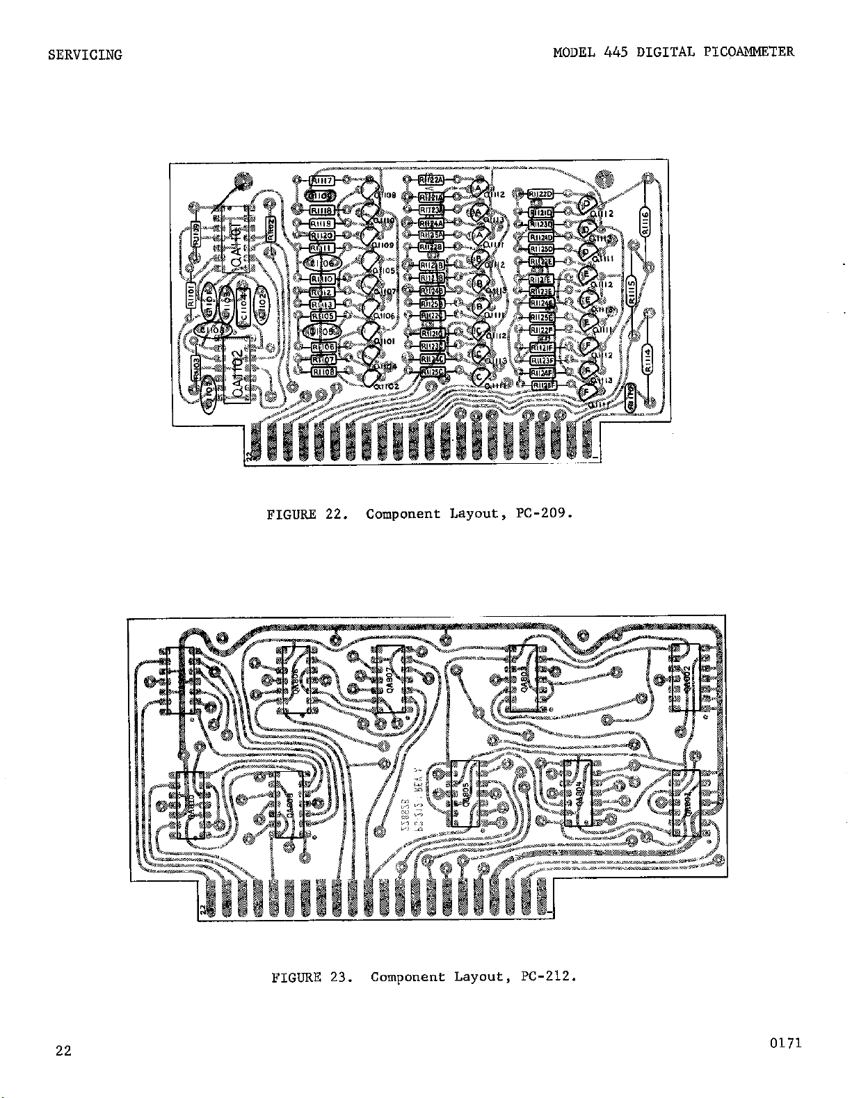
component Layout, PC-209.
22
FIGURE 23.
component Layout, PC-212.
0171
Page 27

MODEL 445 DIGITAL PICOAMMETER
SERVICING
FIGURE 24. Component Layout, PC-214.
FIGURE 25.
0171 23
Component Layout, PC-217.
Page 28

SERVICING
MODEL 445 DIGITAL PICOAMMETER
FIGURE 26.
Component Layout, PC-218.
24
FIGURE 27.
component Layout, PC-219.
0171
Page 29

Page 30

MODEL 445 DIGITAL PICOAMMETER
SERVICING
FIGURE 29.
Component Layout, PC-229.
0171
FIGURE 30. Component Layout, PC-230.
27
Page 31

Page 32

MODEL 445 PICOAMMETER
REPLACEABLE PARTS
REPLACEABLE PARTS
4-l.
REPLACEABLE PARTS LIST.
SECTION 4.
This section contains
a list of components used in this instrument for "ser
reference. The Replaceable Parts List describes the
individual parts giving Circuit Designation, Description, Suggested Manufacturer (Code Number), Manufac-
Abbreviations and Symbols
TABLE 4-l.
A
ampere
F
Fig.
Cb"ar
cero
Cer Trimmer
COtlIP
DCb
oesig.
EAL
ETB
ETT
Carbon Variable
ceramic Disc
ceramic Trimmer
Composition
Deposited Carbon
Designation
Electrolytic, Aluminum
Electrolytic, tubular
Electrolytic, tantalum
CCb
k
I-I
M
Mfr.
MtF
MY
NO.
turer's Part Number, and the Keithley Part Number.
Also included is a Figure Reference Number where
applicable. The complete name and address of each
Manufacturer is listed in the CODE-TO-NAME Listing
following the parts list.
farad
n
ohm
Fig"t-e
pica (10-12)
Class enclosed Carbon
;c
Poly
Printed Circ"if
Polystyrene
kilo (10-3)
Ref. Reference
micro (104)
TC" Tinner Capperweld
leg
(106)
M**“f*Ct”PSr
" "Olt
Metal Film
l.fyl*r
Number
w
NW
WW"*r
watt
Wirewound
Wirewound Variable
4-i. ELECTRICAL SCHEMATICS AND DIAGRAMS. Schematics
and diagranls are included to describe the electrical
circuits as discussed in Section 3. Refer to Table
4-2 which identifies all schematic part numbers in-
cluded.
4-3. HOW TO "SE THE REPLACEABLE PARTS LIST. This
Parts List is arranged such that ehe individual types
of components are listed in alphabetical order. The
parts far the i"str"ment's Main Chassis are listed
folrzed by printed circuit boards and other sub-
assemblies.
4-4. HOW TO ORDER PARTS.
a. Replaceable parts may be ordered through the
TABLE 4-2.
CirC"it Description
Main Chassis
power supply
Polarity Board
Thousand Board
Readout Board
Oscillator Board
Integrator Board
Range Control Board
Range Counter/Decoder
Tube & Driver Board
Output Buffer
output Buffer
Sales Service Department, Keithley Instruments, Inc.
or your nearest Keithley representative.
b. When ordering parts, include the following in-
formation.
1. Instrument Model Number.
2. Instrument Serial Number.
3. Part Description.
4. Schematic Circ"it Designation.
5. Keithley Part Number.
C. All parts listed are maintained in Keiehley
spare parts Stock.
Any part not listed can be made
akilable upon request; -Parts identified by the
Keithley Manufacturing Code Number 80164 should be
ordered directly from Keithley Instruments, Inc.
Schematic Pare No
PC-221
234883
PC-221 234483
PC-207
PC-208
PC-229
234490
234501)
23451E
PC-217 234520
PC-219 234533
PC-214 23454E
PC-212 234553
PC-230
23456D
PC-218 234570
PC-209
234813
0971
29
Page 33

REPLACEABLE PARTS
MODEL 445
r
Series
100
200
300
400
500
600
700
800
900
1000
1100
1200
PC Board Designation Series
Description
Power Supply
Polarity
Board
Thousand Board
Readout Board
08cillator Board
Integrator Board
Range Control Board
Range Counter/Decoder
Tube & Driver Board
Output Buffer Board
Output Buffer Board
MEIF" Chsssis
TABLE 4-3.
Designation Connector
PC-221
PC-207
PC-208
PC-229
PC-217
PC-219
PC-214
PC-212
PC-230
PC-218
PC-209
51204
51205
J1206/51207 41
J1208
51209
51212
51211
51210
.J1216
51202
PC-221
Page No.
37
39
40
i:
46
46
47
i,"
33
30
0971
Page 34

MODEL 445 DIGITAL PICOAMMRTER
REPLACEABLE PARTS
TABLE 4-4.
Mechanical Parts Lisa.
Item No.
1
2
Description
Top Cover Assembly
Cover
Fastener
Bottom Cover’ Assembly
Cover
Fastener
Angle, Rack Assembly
Screw,
Slotted, 10 - 32
Front Panel
Chassis
x l/4
Quantity Per Assembly
Keithley Part No.
17958C
17162C
FA-54
17960C
17957c
FA-54
146248
23000C
230038
0171
FIGURE 31. Mechanical Assembly.
31
Page 35

s (I
j
Page 36

MAIN CHASSIS PARTS LIST
(“1200” Series, E-221)
CAP.4CITORS
REPLACEABLE PARTS
Circuit
msig. Value Rating
Cl201
Cl202 10 @ 20 v
Cl203 10 p 20 "
Cl204 ,004, fl 600 "
Cl205 .047 NF 200 "
Cl206 ,022 fl 400 "
Cl207 .022 p 400 v
Cl208
Cl209 1000 pP 500 v
Cl210 390 pF 500 v
Cl211 .033 p!s 600 "
Cl212 150 pF 500 "
Cl213 3600 pF 500 "
Cl214 22 PF 500 "
Cl215 10 PF 500 "
CU.16 .Ol pF 600 "
Circuit
msig.
.l1201**
5 pF 60" "
.Ol @
600 "
DWXiptiO”
Plug-in contacts
Mfr. Mfr.
TYPe
CerD 72982 ED-5 C22-5P 28
ETT 17554 TSDZ-20-106 C179-10M 28
ETT 17554 TSDZ-20-106 C179-10M 28
CerD 72982 ED-.047 C22-.0047M 28
MY 13050
MY 1305D SMlA C73-.022&l 28
MY 13050
cerD 72982 ED-.01 C22-.OlM 28
POlY 71590 CPR-1000J C138-1OOOP 28
POlY 71590 CPR-3903 C138-39OP 28
MY
Poly 71590 cm-15OJ C138-15OP 28
Poly 71590 CPR-3600J Cl38-3600P '28
POlY 71590
Poly 71590 cm-1O.T C138-IOP 28
cem 72982 m-.01 c22-.OIM 28
CONNECTORS
Code
56289 CPS-550 C62-.033M 28
Mfr.
Part NO. Part NO.
SMlA
SW.4
CPR-22J
Mfr.
Code Part NO.
80164
Keithley
C143-.047M 28
C73-.022M 28
C138-22P 28
Keithley
Part NO.
Fig.
Ref.
see FET Lnput
Fig.
Ref.
28
Card
PI201
51202
51203
.I1204
51205
J1206
51207
51208
51209
Printed circuit contacts, mate
of n201
Receptacle, 44 pins, Rear Card
of 0”tput Buffer Stage PC-209
Not Used
Receptacle, 15
Board PC-207
pins, Polarity
Receptacle, 15 pins, Thousand
Board PC-208
Receptacle, 6
Board PC-229
Receptacle, 15
Board PC-229
pins, Readoue
pins, Readout
91662 02-005-113-6-200
09922
09922
09922
73690 02-006-105-6-200
73690 02-015-105-6-200
09922
09922
09922
09922
PSC 4DD22-12
PSC 45515-12
PSC 4SS15-12
PSC 4SS15-12
PSC 4SS15-12
PSC 4ss**-12
PSC 4SS22-12
m-199
CS-205
cs-175 28
cs-175 28
CS-223 28
CS-222 28
cs-175 28
cs-175 28
CS-182 28
cs-182 28
28
28
0971
33
Page 37

REPLACEABLE PARTS
MODEL 445 DIGITAL PICOAMMETER
MAIN CHASSIS (Cont'd)
CONNECTORS (Cont'd.)
Gil-C"it.
rlesig.
51212
51213
---
51214
__-
51215
51216
51217
---
51218
__-
P1202
Description
Receptacle, 22 pins, Range
Mfr.
Mfr.
code Part NO.
09922 PSC 4SS22-12 CS-182
Keithley
Part No.
Control Board PC-214
Receptacle, triaxie1, INPUT
95712
Plug, triaxisl, mate of 51213 95712
Receptacle, 50 pins, PRINTER/
02660
33050-2-m-34
30197-l
CS-181
m-141
57-40500-1 CS-221
CONTROL Connector
'Plug, mate of J1214
02660
57-30500-l CS-220
Binding Post, LO 58474 DF21BC BP-11B
Receptacle, 44 pins, Front
09922 PSC 4DD22-12 CS-205
Card of Output Buffer Stage, PC-21Q
Binding Post, GND 58474 DFZlGC BP-116
Shorting Link for LO & GND Posts 24655 938-L BP-6
Receptacle, Microphone, ANALOG
02660
SO-PCZF CS-32
OUTPUT
Plug, mate of 51218 (Supplied) 02660 SO-MCZM CS-33
1 pin connector, mete to .I501
80164
CS-185 lx-185
FFg.
Ref.
28
3
3
3
28
Circuit
Des&.
TYPe
Mfr. Mfr.
Cade
Part No. PaIT NO. Ref.
Keithley Fig.
L!lZOl Silicon 01295 lN64.5 RF-14 28
D1202 Silicon 01295 lN645 RF-14 28
D1203 Silicon 01295 lN645 RF-14 28
~1204 Silicon 01295 1~645 RF-14 28
01205 SilkOIl 01295
D1206
D1207
D1208
~1209
01210
DlZll Silicon
D1212
01213 Silicon
D1214
01215 Silicon
D1216 SiliClXl
01217 SiliCOl?
Dl218 Silicon
Silicon 01295
SFliCOlI
Silicon
Silicon
Silicon
01295
01295
01295
01295
02735
Silicon
02735
02735
zener
84970 VR47
01295 113645
01295
02735
02735
1~645
lN645
18645
lN914
lA645
lN3255
lN3255
1133255
1~645
lN3255
IN3255
RF-14 28
RF-14
28
RF-14 28
RF-14
RF-28
RF-14
RF-17
RF-17
RF-17
DZ-30
RF-14
RF-14
RF-17
RF-17
28
28
28
28
28
28
28
28
28
28
28
LAMPS
circuit
Desig.
DS1201
Description
Range Changing Pilot Light,
Mfr. Mfr.
Code Part No. Part NO. Ref.
91802 2100 series
Keithley
PL-46
Fig.
2
34
Page 38

MODEL 445
REPLACEABLE PARTS
MAIN CHASSIS (Cont’d)
RELAYS
~1201(A
K1202 (1
8. B) Reed
K1203 ‘1
K1204 PI
K1205 ”
K1206
”
K1207 ta
K12OS ”
circuit
oesig.
23430B
PC-207
Mfr.
Cade
Relay
Reed Relay
Reed Relay
Reed Relay
Reed Relay
Reed Relay
Reed Relay
Reed Relay
27682
27682
27682
27682
27682
27682 525-0002
27682
27682
PRINTED CIRCUIT SUB-ASSSMBLIES
Description
Input FET P.C. Board, with components.
Polarity P.C. Board, with componenes.
less components.
Mfr.
Part No.
525-0002
525-0002
525-0002
525-0002
525-0002
525-0002
525-0002
Eceithley
Part No.
RL-34
RL-34
RL-34
RL-34
RL-34
RL-34
RL-34
RL-34
Fig.
Ref.
28
2s
28
2s
28
28
28
28
lceithley
Part NO.
23730B
PC-207
22875B
PC-208
PC-209
PC-212
PC-214
PC-217
PC-218
PC-219
PC-229
PC-230
Thousand P.C. Board, with ccqmnents.
Output Suffer P.C. Board, Model 4401, vith components.
less components.
Range Counter/Decoder P.C. Board, with components.
less companencs.
Range Control P.C. Board, with components.
less components.
Oscillator P.C. Board, with components.
less components.
Output Buffer P.C. Board, Model 4401, with components.
leas components.
Integrator P.C. Board, with com,,one”ts.
less componenes.
Readout P.C. Board, with coqmnents.
less components.
Tube & Driver P.C. Board, with components.
less camponents.
PC-208
2287SB
Iv-209
228828
PC-212
22892B
PC-214
22895B
PC-217
230618
PC-218
23065B
PC-219
230bSB
PC-229
23628C
PC-230
23633B
0971
35
Page 39

REPLACEABLE PARTS
MAIN CHASSIS (Cont'd)
RESWI'ORS
MODEL
445 DIGITAL PICOAMMETER
R1201
R1202
R1203**
R1204
R1205
R1206
R1207
R1208
R1209
R1210
R1211
R1212
R1213
R1214
R1215
R1216
R1217
R121S
R1219
R1220
R1221
R1222
R1223
R1224
R1225
Value
10 MO
10 kn
100 kR
15 kn
100 n
18.2 ki,
500 n
18.2 kn
22 kn
4.7 kn
4.7 kfl
680 0
3.3 k0
100 n
470 n
100 R
116.67 il
4.75 kR
1.1667 kfl
11.667 ki7
115
k0
1.15 Mn
10 Mn
1.5 Mn
100 Mil
Rating
l%, l/2 W
20%, 2 w
lO%, l/4 w
l%, l/0 W
lO%, l/2 w
l%, l/8 w
?20%, 2 w
1%.
1/a w
lO%, l/4 w
lO%, l/4 w
lO%, l/4 w
lO%, l/4 w
lo%, l/2 w
lO%, 2 w
lO%, 2 w
lO%, l/2 w
O.l%, 1 "
l%, l/2 w
O.l%, 1 w
O.l%, 1 w
l%, l/2 w
l%, l/2 w
l%, l/2 w
l%, l/2 w
l%, 2 w
Mfr.
Type
DCb
Code
91637
WWVtW 71450
camp
MfF
camp
MW
Cermet
MtF
camp
07716
01121
07716
71450
07716
44655
COl"p 44655
camp
COIBP
COlllp
COtlIP
CO¶V
COtlIP
ww
MU
WI?
ww
MtF
Mm
DCb
DCb
DCb
44655
44655
01121
01121
01121
01121
01686
07716
01686
01686
07716
07716
91637
91637
91637
Mfr.
PBrt No.
DCF-l/2
INS 115
CEA
EB
CEA
551
CEA
RC07
RC07
RC07
RC07
EB
HB
HB
EB
7040
CEC
7040
7040
CEC
CEC
DCF-l/2
DCF-l/2
DC-2
Keithley
Part No.
RlZ-10M
RPSO-1OK
R88-15K
Rl-100
R88-18.2K
RP72-500
R88-18.2K
R76-22K
R76-4.7K
R76-4.7K
R76-680
Rl-3.3K
R3-100
R3-470
Rl-100
R70-116.67
R94-4.75K
R70-1.1667K
R70-11.667K
R94-115K
R94-1.15M
RlZ-10M
RlZ-1.5M
R14-100M
Fig.
Ref.
28
28
28
28
28
28
28
28
28
28
28
28
2s
28
28
28
28
28
28
28
2s
28
2s
28
R1226
R1227
R1228
R1229
R1230
R1231
R1232
R1233
R1234
R1235
R1236
R1237
R1238
circuit
Desig.
s1201
-_-
51202
S1203
S1204
15 lm
109 n
4.75 kR
250 kfi
5 kO
50 kfl
500 kfl
560 0
1 k0
1 kn
249 kiZ
500 kfl
1 kR
l%, 1 w
+3-O%, l/R W
l%, l/2 w
?20%, 2 w
20%, 2 w
220%, 2 w
*20%, l/4 w
10%. l/2 W
20%, 2 w
20%, 2 w
lO%, 112 W
120%, 114 w
20%, 2 w
DeSCriptiO"
Rotary Switch, FILTER
Knob Assembly, Filter Switch
Toggle Switch, RANGE 10-2/DOWN
Toggle Switch, RANGE HOLD/AUTOMATIC
Toggle Switch, ZERO cHEcK/OPmATE
DCb
GCb
MtF
C~~llWt
wvar
91637
80164
07716
71450
71450
CetXEt 71450
CbVar
COIl?p
71450
0,1121
WW"X 71450
WWVU
MtF
CbVar
wwvar
SWITCHES AND CONTROLS
71450
07716
71450
71450
DC-1
230928
CEC
550
INS 115
550
Type-45
EB
INS 115
INS 115
CEC
GC45
INS 115
Mfr.
R13-15M
230928
R94-4.75K
RP79-250K
AP50-5K
RP74-50K
RP73-500K
Rl-560
RPSO-1K
RPSO-1K
R94-249K
RP75-500K
RPSO-1K
Keithley
Code Part No.
80164
SW-280
80164 209338
80164
80164
80164
SW-277
w-236
88-236
28
28
28
28
28
28
28
28
28
28
28
28
28
Fig.
Ref.
2
2
2
2
** R1203 is part of FET I"p"t Card
36
0971
Page 40

MODEL 445 DIGITAL PICOAMMETER
REPLACEABLE PARTS
MAIN CHASSIS (Cont'd)
SWITCHES AND CONTROLS (Cont'd.)
circuit
Desig.
51205
Rotary Switch, DISPLAY RATE (see
Description
also R1237)
-._
__-
circuit
Desig.
QlZOl**
Q1202**
Knob Assembly, Display Rate Control
Screwdriver Adjust potentiometer,
ZERO
ADJUST
(81207)
Mfr.
Code
80164
80164
Q1203 07263
Q1204 07263
Q1205 04713
41206 71279
**Transistors Q1201 and Q1202 are matched
TRANSISTORS
Mfr.
Part NO.
S17638
S17638
2133904
ES-5321
POWER SUPPLY PARTS LIST
("100" Series, PC-221)
CAPACTTORS
Mfr.
Keithley Fig.
code Part NO. Ref.
71450 RP75-500K 2
80164
71450 RPSO-1OK
Keiehley
Part NO.
2
2
Fig.
Ref.
28
28
TG-33
TG-33
TG-47
TG-54
28
28
2s
28
Keithley
Part No.
C93-ZOOOM
czz-11OOP
Fig.
Ref.
28
28
C22-150P 28
C177-ZOOM 28
C177-ZOOM 28
C177-ZOOM 28
C177-ZOOM 28
C179-1.2l.l 28
C22-5P 28
C3-125M
C3-125M
C173-15M
2s
28
28
C94-500M 28
Value klti*g
Cl01
Cl02
Cl03
Cl04
Cl05
Cl06
Cl07
2000 fl
100 pF
150 pF
200 pF
200 fl
200 p
200 @J
Cl08 1.2 pE
Cl09
Cl10
Cl11
Cl12
Cl13
Cl14
5 PF
125 ,iF 15 v ETB 73445 C42b
125 (IF
15 pF
500 plJ
68 PF
Mfr. Mfr.
Type
15 v
600 "
600 V
35 v
35 v
35 v
EAl
Ce?Sl
CerD
EAl
EAl
BAl
35 " EAl
20 " ETT
Code
72982
72982
90201
90201
90201
90201 MTVZOON35PDN
17554 TSDl-20-125
Pat-t No.
36-750-ZOOO-15C
ED-100
ED-150
MTVZOON35PDN
MTVZOON35PDN
MTVZOON35PDN
600 V CerD 72982 ED-5
15 v
300 v
25 V
ETB 73445 C42b
EAl
90201 PTC-015-N-300-P-3-E
EAI 56289 89D234
DIODES
CiX”it
Deeig.
‘fw
Mfr.
Code
Mfr.
Pare NO.
Keithley
Fig.
Part N". Ref.
DlOl Silicon 13327 1134139 RF-34 28
0102 Silicon 13327 lN4139 RF-34 28
Ill03 Silicon 01295 lN645 RF-14 28
0104 Silicon 01295 lN645 RF-14 28
D105 SiliCO" 01295 lNb45 RF-14 28
0106 SiliCO" 01295 lN645 RF-14 28
II107 Silicon 01295 lN645 RF-14 28
0108 Silicon 01295 lN645 RF-14 28
D109 Silk"" 01295 lN645 RF-14 28
DllO zener 04713 lN936 m-5 28
0971
37
Page 41

REPLACEABLE PARTS
MODEL 445 DIGITAL PICOAMMETER
POWER SUFTLY (Cont'd)
DIODES (Cont'd.)
CirCUit
maig.
Dill
0112
D113
CitXUit
msig.
FlOl (117V)
FlOl (234V)
--_
PI01
SlOl
5102
TlOl
Type
Silicon
Silicon
Silicon
Mfr.
Code
02735
01295
01295
Mfr.
Part NO.
183255
113645
lN645
MISCELLANEOUS PARTS
Mfr.
Mfr.
Description Code Part No. Part NO. Ref.
Fuse, slow blow, 3/8 A
71400
Type
MDL
Fuse, quick acting, zoom.4 75915 361.200 FU-24
Fuse Holder 75915
Cord Set, 6 feet
Slide Switch, 117-234V
Toggle Switch, POWER
Power Transformer
93656
80164
80164
80164
342012 FH-3
4638-13
SW-151
SW-265 SW-265
TR-114
RESISTORS
Value
Rating
TYPO
Mfr.
Code Part NO. Part No. Ref.
Mfr.
Keiehley
Part NO.
RF-17
RF-14
RF-14
Keithley Fig.
FU-18
co-5
SW-151
TR-114
Keithley
Fig.
Ref.
28
2s
28
3
3
3
I3
2
19
Fig.
RlOl 6.8 kC
R102
R103
R104
RI05
0.2 n *lo%, 4.25W TCU
10 kC
1.1 kR
1 kR lO%, l/4 W camp 44655 RCO7
R106 100 n
R107
RlOS
RI09
RI10
Rlll
150 a
33 kC
30 l%, l/2 W
680 a
3.3 kfl
lO%, l/4 w CCX&P 44655
l%, l/8 W Mm
l%, l/S W MtF
l%, l/S w
l%, l/8 W
MtF
MtF
lO%, l/4 W
DC%
lO%, l/4 W
COlllP
IO%, l/4 w
R112 4.7 kfl 10%, l/4 w
R113 3.3 kR
R114
R115
R116
R117
4.75 k0
2 kR
8.06 kC
15 kC lo%, l/4 w COlllp
RllS 7.5 kC l%, l/8 W
lO%, l/4 w
l%, l/8 w
20%, 2 w
l%, l/8 W MW
MtF
R119 33 kR lO%, l/4 w COUV
R120
R121
R122
RI23
R124
RI25
RI26
3n
33 kR
33 kC
7.32 kR
82 n
1 Mn
100 k0
RI27 56 kfi
R128 80.6 kR
l%, l/2 w
lO%, l/4 w
lO%, l/4 W
l%, l/8
W
lO%, l/2 w
lO%, l/4 w
lO%, l/4 w
IO%, l/4 w
1%. l/2 w
DCb
camp
MtF-
camp
camp
camp
91637 CW-2 R151-0.2
x07 R76-6.8K
07716
CEA
07716 CEA
R88-10K
R88-1.x
28
28
28
28
R76-1K 28
07716
07716
44655
91637
CEA
CRA
RC07 R76-33K
DCF-l/2
44655 RCO7
44655
RC07 R76-3.3K
44655 RC07 R76-4.7K
R88-100 28
RES-150
28
28
RlZ-3 28
R76-680 28
28
28
44655 RCO7 R76-3.3K 28
07716 CEA REE-4.75K
71450 INS 115 RP50-2K
07716 CEA RES-8.06K
44655 RC07 R76-15K
07716 CEA REE-7.5K
44655 RC07
R76-33K
91637 Lxx-l/Z RlZ-3
44655
44655
07716 CEA
01121
44655 RC07
44655 RCO7
RC07 R76-33K
RC07 R76-33K
R88-7.32K
EB
Rl-82
R76-1M
R76-l00K
44655 RC07 R76-56K
07716
CRC R94-80.6K
28
28
28
28
28
28
28
28
28
28
28
28
28
2s
28
0971 38
Page 42

MODEL 445 DIGITAL PICOAMMETER
REPLACEABLE PARTS
POWER SUPPLY (Cont'd)
RESISTORS (Cont'd.)
circuit
Desig.
R12Y
R130
F.131
R132
R133
"8lW Rating
7.32 kn l%, l/8 W
1.5 kR
1 kn
lo%, l/4 W
lO%, l/4 w
12 k12 lO%, l/4 w
10 kn lO%, l/4 w
TYW
MW
cow
COUlP
COUlP
camp
Mfr. Mfr.
Code Part NO. Part NO. Ref.
07716 CBA K88-7.32K
44655 KC07
44655
RC07
44655 RC07 R76-12K
44655 KC07 R76-10K 28
Keithley Fig.
28
~76.1.5K 28
R76-1K
28
28
TRANSISTORS
CirC"it
Desig.
q101
q102
"103
a104
Q105
Q106 07263
QlO7 02734
QlO8 07263
q109 07263
QllO
Mfr. Mfr.
Code
Part No.
2N3565
40317
2133565
2N3565
07263
S1763S
Keithley Fig.
Part NO.
TG-68
lx-54
z-39
TG-39
TG-33
TG-39
Ref.
28
28
28
28
28
28
TG-43 28
m-39 28
m-39 28
TG-33 28
Qlll 02734 40319 TG-50 28
q112 07263 517638 TG-33 28
Q113 07263 517638 TG-33 2s
q114 07263 2N3565 x-39 28
q115 07263 2N3565 x-39 28
Q116 07263 517638 u-33 28
Q117 07263 S17638
q11*
4119
02735 40346 x-44 28
02735 40-346
TG-33 28
TG-44 28
Ql20 07263 2N3565 TG-39 28
POLARITY BOARD PARTS LIST
("200" Series, X-207)
CAPACITORS
Circuit
msig.
C201
"EllW Rating
150 PF 600 " CerD 72982
TYV=
INTEGRATED
Circuit
tlesig.
QA201
QA202 quad 2 Input Gate 04713 MC724P IC-5 20
qA203 Quad 2 Input Gate 04713 MC724P IC-5 20
QA204 qua* 2 Input Gate 04713 MC724P ic-5 20
QA205 Quad 2 I"p"t Gate 04713 MC724P K-5 20
qb.206
QA207 Dual 3 InpUt suffer, non-inverting 04713 MC788P IC-6 20
Dual J-K Flip-Flop
Dual J-K Flip-Flop 04713
Description
.wr.
Mfr.
Cc& Part NO. Part NO. Ref.
ED-150 C22-15OP 20
CIRCUITS
Mfr. Mfr. Keithley Fi,S.
Code Part NO. Part NO. Ref.
04713
MC79OP n-8
MC790P IC-8
Keithley
Fig.
20
20
0971
39
Page 43

REPLACEABLE PARTS
MODEL 445 DIGITAL PICOAMHSTER
POLARITY BOARD (Cont'd)
LAMPS
circuit
Deaig.
DS201
cirlxit
DeSig.
R201
R202
R203
R204
circuit
uesig.
Q201
Q202
circuit
Desig.
Description
tpolarity Pilot Light
Value
270 C
2.2 kC
1.5 kR
1.5 kC
RattIll:
10%, l/4 w
lO%, l/4 w
lO%, l/4 w
lO%, l/4 w
Mfr.
Code
02735
02735
Description Code
Mfr.
Code
91802
RESISTORS
Mfr.
Type
COlllP
COUIP
COUIP
COUIP
Code
44655
44655
44655 RC07 R76-1.5K 20
44655
TRANSISTORS
Mfr.
Part No.
2N5184
2N5184
THOUSAND BOARD PARTS LIST
("300" series, PC-208)
INTEGRATED CIRCUITS
Mfr.
Mfr.
Part No.
2330 Series
Mfr.
Part No. Part No. Ref.
RC07 R76-270
RC07 R76-2.2K 20
RC07 R76-1.5K 20
Mfr. Keithley
Part No. Part NO. Ref.
Keithley
Part NO.
TG-67
TG-67
Keithley
Part NO.
PL-43
Keithley
Fig.
Ref.
20
Fig.
20
Fig.
Ref.
20
20
Fig.
QA301
QA302
QA303
QA304
Cil?C"i+Z
rlesig.
R301
R302
circuit
Desig.
Q30
Dual J-K Flip-Flop
Dual J-K Flip-Flop
04713
04713
MC79OP
MC79OP IC-8
Ouad 2 positive logic Nor Inpur Gate 04713 MC724P
Hex 1nverter
04713
MC789P
LAMPS
Description
Mfr.
Code Part NO.
Mfr.
Pilot Light, front panel thousands tube 80164 PL-42
RESISTORS
Value
1.5 kfl
100 kC
Rating
lO%, l/4 w
lO%, 1 w
Type
COtlIP
COlllp
Mfr.
Code Part NO. Part NO. Ref.
44655 RCO7
01121
Mfr.
GB
TRANSISTORS
Mfr.
Code
02735
Mfr.
Part No.
2N5184
Keithley
Part No.
TG-67
IC-8
21
21
IC-5
IC-7
Keithley
21
21
Fig.
Part NO. Ref.
PL-42 21
Keithley Fig.
R76-1.5K
RZ-100K
21
21
Fig.
Ref.
21
40 0971
Page 44

MODEL 445 DIGITAL PICOAMMETER
REPLACEABLE PARTS
RFADOUT BOARD PARTS LIST
(“400” Series, PC-229)
CONNECTORS
circuit
Desig.
P401
P402
CiK"it
msig.
QA401
QA402
QA403
QA404
QA405
QA406
QA407
QA408
QA409
QA410
QA411
QA412
QA413
QA414
QA415
QA416
QA417
DeSCt+tiO" Code
mug, 6 pins, connects to 51206
Plug, 22 pins, Connects to J1207 73690 02-015-105-6-200
DeSCripCiO"
Dual J-K Flip-Flop
Dual J-K Flip-Flop
Dual J-K Flip-Flop
Dual J-K Flip-Flap
Dual J-K Flip-Flop
Dual J-K Flip-Flop
Quad 2 Input Gate
Quad 2 Input GBL~
Dual J-K Flip-Flop
Dual J-K Flip-Flop
Dual J-K Flip-Flop
Dual J-K Flip-Flop
Dual J-K Flip-Flop
Dual J-K Flip-Flop
Decimal Decoder/Driver
Decimal Decoder/Driver
Decimal Decoder/Driver
Mfr. Mfr.
73690
INTEGRATED CIRCUITS
02-006-105-6-200
Mfr.
Code
04713
04713
04713
04713
04713
04713
04713
04713
04713
04713
04713
04713
04713
04713
07263
07263
07263
Part NO.
Mfr.
Part NO.
MC791P
MC791P
MC791P
MC79OP IC-8
MC790P
MC79OP IC-8
MC724P
MC724P IC-5
MC79OP
“C790P
MC79OP
MC79OP
MC79OP
MC790P
U6B996079X
U6B996079X
U6B996079X n-3
Keithley
Part NO.
c-223
a-222
Keithley
Part NO. Ref.
IC-9
IC-9
IC-9
IC-8
U-5
IC-8
IC-8
IC-8
IC-8
K-8
E-8
xc-3
E-3
Fig!.
Ref.
29
29
Fig.
29
29
29
29
29
29
29
29
29
29
29
29
29
29
29
29
29
READOUT TUBES
CirCUie
Desig.
v401
“402
v403
Value
R401 10 ksl 5%, l/2 w COlllp
~402 10 kn 5%, l/2 w
R403 10 kn 5%, l/2 w
Circuit
Desig. Rating
c501 .0022
c502 ,001 pF 100"
c503 4.5-25 pF 500"
c504 22 pF 500"
c505 470 pF 600”
Description
"nits Readout Tube
Tens Readout Tube
Hundreds Readout Tube
Rating
p
100"
OSCILLATOR BOARD PARTS LIST
("500" Series, W-217)
POlY 13934 E3FR-222-1-C C152-.0022M
P"ly 13934 E3FR-222-1-C C152-.OOlH 25
cer Trimmer 71590 82282 C76-4.5-25P 25
Mica 84171 DM15-220J c21-22P 25
CerD 72982 ED-470 CZZ-470P 25
Mfr.
Code
80164
80164
80164
RESISTORS
TYP
COUlP 01121 EB R19-10K 29
COtlIP
CAFWITORS
Mfr.
Part NO. Part ND.
___
-__
_-_
Mfr.
Code Part NO.
01121 EL3
01121 E" R19-10K 29
Mfr. Mfr. Keithley
Code
Mfr.
ParI2 NO. Part NO. Ref.
Keithley
E”-841 29
E”-841
E”-841
Keithley
Pal-t NO. Ref.
R19-10K 29
Fig.
Ref.
Fig.
Fig.
29
29
25
0971
41
Page 45

REPLACEABLE PARTS
OSCILLATOR BOARD (Cont'd)
CAPACITORS (Cant'd.)
MODEL 445
DIGITAL
PICOAMMETER
Cil-CUit
Desig.
C506
c507
C508
Circuit
Desig.
D501
D502
0503
J501
QA501
QA502
y501**
Value
220 pF 600"
4.7 tlF 2OV
10 P 2ov
Diode, Silicon, lN645 01295 RF-14 25
Diode, Silicon, lN645 01295 RF-14 25
Diode, Silicon, lN914 01295 RF-28 25
Varicon Contact 73690 02-001-113-6 m-224 25
Quad 2 positive logic Nor Input Gate
Quad 2 positive logic Nor Input Gate
Crystal, 60 Hz 80164 CR-1 CR- 1 25
Rating
Type
CerD 72982 ED-220 czz-22OP 25
ETT 05397 K4R7JZOK CEO-4.7M 25
ETT 17554
MISCELLANEOUS
Description Code Part NO. Pat-t No. Ref.
Crystal, 50 HZ 80164 CR-2 CR-2 25
RESISTORS
Circuit
Desig. Value Rating Type
R501 3.3 ksl
R502
33 kfl
R503 68.1 0
R504 4.99 k!l
R505
1 kfi
lO%, l/4 w C‘XIIP 44655 RC07 R76-3.3K
lO%, l/4 w COlDp 44655 RC07 R76-33K
l%, l/8 W
I%, l/8 W
MtF 07716
MW
lO%, l/4 w COUlP 44655 RC07
Mfr.
Mfr.
Keirhley
Code Part NO. Part NO.
TSD2-‘JO-106
Cl79-IOM 25
PARTS
Mfr. Mfr.
04713
04713
Mfr.
Code Pare NO. Part NO. Ref.
MC724P U-5
MC724P IC-5 25
Mfr.
CEA
07716
CEA
Keithley Fig.
Keithley Fig.
R88-68.1
R88-4.99K
R76-1K
Fig.
Ref.
25
25
25
25
25
25
R506
R507
1 kR
1 kR
lO%, l/4 w
l%, l/8 w
R508 470 a lo%, l/4 W
R509 4.7 k0 lO%, l/4 W
R510 56 kfl
R511 4.7 k0
R512 470 n
R513 680 0
ix514 470 R
R515 237 n
R516 1 kfl
R517 4.99 kfi
R518 56 kfi
R519 237 0
R.520 3.3 kG.
R521 6.8 k0
R522 1.5 kfl
R523 1 kfi
R524 1 kR
R525 10 kfi
R526 1 kn
R527 3.9 k0
R528 3.9 kR
R529 330 a
R530 1.5 kn
lO%, l/4 w
lO%, l/4 IJ
lO%, l/4 iJ
10%) I/ 4 w
lO%, l/4 w
l%, l/8 w
l%, l/8 W
l%, 118 W
lO%, l/4 w
l%, l/8 W
IO%, l/4 w
lO%, l/4 w
lO%, l/4 w
lo%, l/4 w
lO%, l/4 W
lO%, l/4 w
lO%, II4 w
lo%, 114 w
lo%, l/4 w
IO%, l/4 w
lO%, l/4 w
COlllP 44655
MtF
07716
CCXUP 44655
COl?lP
COtlIp
44655
44655
COmp 44655
C‘Xlp 44655
COlllP 44655
COlilp 44655
MW 07716
MtF 07716
MC? 07716
COUIP 44655
MtF 07716
COUtP 44635
camp 44655
COUIP 44655
camp 44655
c olnp 44655
COmp 44655
CLXV 44655
COtlIp 44655
COUIP 44655
COmp 44655
COtlIp 44655
RC07
CEA
R76-1K
R88-1K
RC07 R76-470
RC07
X76-4.7K
KC07 R76-56K
RC07 R76-4.7K
RC07 R76-470
RC07
R76-680
RC07 R76-470
CEA
CEA
CM
R88-237
Rfm-1K
R88-4.99K
RC07 R76-56K
CEA
R88-237
RC07 R76-3.X
RC07
R76-6.8K
RCO7 R76-1.5K
RC07 R76-1K
RC07 R76-lK
RC07
RC07
RC07
R76-10K
R76-1K
R76-3.9K
RC07 R76-3.9K
RC07
RC07
R76-330
R76-1.5K
25
25
25
25
25
25
25
25
25
25
25
25
25
25
25
25
25
25
25
25
25
25
25
25
25
42
0971
Page 46

MODEL 445 DIGITAL PICOAMMETER
REPLACEAULE PARTS
OSCILLATOR BOARD (Cont'd)
RESISTORS (Cont'd.)
circuit
Desig.
R531
R532
R533
R534
R535
Value
5.6 k0
4.7 k0
10 0
1.5 Id7
1 kn
R536 47 n
K537
K538
circuit
oesig.
33 n
4.02 k0 l%, l/8 W MU 07716
Q501
Q502
4503
Q504
Q505
Q506
Q507
Q508
Q509
4510
Q511
Q512
Q513
Q514
Kating
lo%, l/4 w
lo%, l/4 w
lo%, l/4 w
lO%, l/4 w
l%, l/S w
lO%, l/4 w
lO%, l/4 w
Mfr.
Code
07263
07263
07263
07263
07263
07263
07263
07263
07263
07263
07263
07263
07263
03508
Mfr. Mfr.
Type
camp
camp
camp
camp
MCF
CO"p
camp
Code
44655 x07 R76-5.6K 25
44655
RC07 R76-4.X 25
44655 RC07 R76-10
44655
07716
RC07 K76-1.5K 25
CEA
44655 KC07 R76-47 25
44655
RCO7
CEA
Mfr. Keithley
Part NO. Part NO.
2N5134 'X-65
2N5134 Z-65
2N5134 m-65
2N5134 X-66
2N5134 X-65
m5p9 W-66
2N5134 X-65
2N5139 W-66
2N5134 W-65
2N5134 TG-65
2N5134 TG-65
2N5134 TG-65
2N5134 W-65
2N2646 m-52
Keithley
Fig.
Part NO. Part NO. Leaf.
25
K88-1K
K76-33
25
25
R88-4.02K 25
Fig.
Ref.
25
25
25
25
25
25
25
25
25
25
25
25
25
25
C601
C602
C603
C604
C605
C606
C607
C608
C609
C610
C611
C612
C613
C614
Value Rafing
100 pF 600V
10 pF 5oov
0.082 @ 1oov
10 @J 2ov
220 pF 600~
220 pF 600V
.0047 ,lF 600V
0.1 I*F 250v
10 w 2OV
22 pP 1000"
0.1 I*F 250V
10 ,.F 2ov
10 ,lF 2ov
22 ,9 1ov
INTEGRATOR
("600" Series, PC-219)
BOARD PARTS LIST
CAP*CITORS
Mfr.
TYW
Code
cero 72982 ED-100
Mfr.
Keithlfy
Part NO. PaIT NO.
C22-1OOP 27
Poly 71590 cm-1OJ C138-LOP 27
l%ly 13934
E3FR-222-1-C
ETT 17554 TSDZ-20-106
CeHl 72982 ED-220
cero 72982 ED-220
CerD 72982 ED-.0047
73445 C280AEfPlOOK
ETT 17554 TSiX-20-106
certl 56289 56AQ22
73445 C280AED100~
C152-.082M 27
C179-10M 27
czz-22OP 27
CZZ-22OP 27
CZZ-.0047M
C178-.lM 27
C179-10M
c72-22P
c17z3.m 27
ETT 17554 TSDZ-20-106 C179-10M 27
ETT 17554 TSDZ-20-106
ETT 17554 TSDZ-10-226
C179-10M 27
C180-22M
Fig.
Ref.
27
27
27
27
0971
43
Page 47

REPLACEABLE PARTS
MODEL 445 DIGITAL PICOAMMETER
INTEGRATOR BOARD (Cont'd)
circuit
Desig.
0601
0602
0603
D604
0605
D606
0607
~608
D609
~610
Type
7.ener
7.ener
Silicon
Silicon
Silicon
Silicon
SiliCOll
Silicon
Silicon
Silicon
Mfr. Mfr.
Code Pa-C No.
04713 lN936
04713
07263
07263 2N3565
01295 lN645
01295
01295
01295
01295
01295
0611 Silicon 01295
0612 SiliCCXl 01295
D613 Silicon 01295
D614 SiliCO" 01295
0615 Silicon 01295
INTEGRATED CIRCUITS
Description
QA601
QA602
QA603
QA604
Integrated Circuit
Integrated Circuit
High Speed Differential Comparator
Quad 2 InPUt Gate
DIODES
Keithley
Fig.
Pat-t NO. Ref.
m-5 27
18936
2N3565
DZ-5 27
w-39 27
TG-39 27
RF-14 27
1~645
lN914
lN914
lN645
lN645
lN645
lN645
lN914
lN914
lN645
Mfr.
Code
Mfr.
Part NO.
RF-14 27
RF-28 27
RF-28 27
RF-14 27
RF-14 27
RF-14 27
RF-14 27
RF-28
27
RF-28 27
RF-14 27
Keifhley
Part NO.
Fig.
Ref.
12040 LM-201 xc-2 27
12040 m-201 x-2 27
07263
04713
65B771039X
MC724P
IC-4
IC-5
27
27
CilTUilZ
Desig.
~601
R606
R607
~608
R609
~610
R613
R614
R615
R616
R617
R618
Ml9
R620
R621
R622
R623 4.7 kfi
R624 49.9 kfi
R625
Value Rating
10 lin 10%. l/4 W
10
kfl
*
7.5 kil
7.5 kfi
7.5 k*
Not Used
499 0
49.9 ksl
680 C?
680 fi
33 kR
4.7 kIl
33 kn
4.7 kn
4.7 k*
l%, l/S w
I%, l/8 W
l%, l/S w
l%, l/8
l%, l/S w
lO%, l/4 w
lo%, l/4 w
lO%, l/4 w
1056, l/4 w
lO%, l/4 w
lO%, l/4 w
10%. l/4 w
10%; l/4 w
l%, 1/a w
100 kO lO%, l/4 w
* Nominal value, factory selected.
..,
W
RESISTORS
Mfr.
Type Code
corn
44655
MtF' 07716
MtF 07716
MtF
MU
07716
07716
cermet 73138
MfF 07716
Mm 07716
MtF 07716
MW 07716
i%L%let 73138
COtlIp
44655
MtF 07716
MtF 07716
camp 44655
camp 44655
COUlp 44655
camp 44655
COlllp 44655
COtlIP 44655
COWI 44655
COIMP 44655
MtF 07716
COllp 44655
RC07
CEA
CEA
CEA
CEA
77PRlOK
CEA
cm
CEA
CEA
77PRlOK
RCO7
CEA
CEA
RC07
RCO7
RC07
ix07
RC07
RC07
RCO,
RC07
CEA
RC07
Keiehley
Par? No.
R76-10K
R88-*
R88-7.5K
R88-7.5K
R88-7.5K
RP64-1OK
R88-*
Fig.
Ref.
27
27
27
27
27
27
27
R88-7.5K 27
RS8-7.5K
27
R88-7.X 27
RP64-10K
27
R76-10K 27
R&x3-499 27
R88-49.9K 27
R76-680 27
R76-680 27
R76-33K 27
R76-4.7K 27
R76-33K 27
R76-4.7K 27
~76-4.7K 27
R76-4.7K 27
R88-49.9K
2.
~76-1OOK 2,
44
0971
Page 48

MODEL 445 DIGITAL PICOAMMETER
REPLACEABLE PARTS
INTEGRATOR BOARD (Cont'd)
RESISTORS (Cont'd.)
Value Rating
R626
R627
R628
237 0
301 kn
1%. l/S w
l%, l/S w MW 07716
47 n lO%, l/4 w
R629 100 kn lO%, l/4 w
R630 158 n
R631
R632
R633
R634
R635
~636
158 R
200 R
301 kR
1.5 kn
47 n
2.2 kn
R637 47 0
R638
47 R
R639 1.5 k.Q
R640 1.5 kR
R641
R642
R643
R644
R645
R646
R647
R648
R649
R650
100 R
10 0
3.01 k0
1 kn
5.6 kR
5.6 kO
10 a
402 n
200 n
402 0
l%, l/8 W
l%, l/8 w
L!ZO%, 314 w
1%, l/8 W
lO%, l/4 w
lO%, l/4 w
lO%, l/4 w
lO%, l/4 w
lO%, l/4 w
lO%, l/4 w
lO%, l/4 w
lo%, l/4 w
lO%, l/4 w
l%, l/8 W MtF 07716
l%, l/S w Mm 07716
lO%, l/4 w
lO%, l/4 w
lO%, l/4 w
l%, l/8 w
i20%, 314 w
l%, l/8 "
Type
Code
MW 07716
COllQ2 44655
camp 44655
NW 07716
MtF 07716
iXrTTlet 73138
MtF 07716
COtlIp 44655
camp 44655
COlRp 44655
COTlIp 44655
COW 44655
COpJ 44655
COlllp 44655
COOlp 44655
COtlIp 44655
COlp 44655
COmp 44655
COlllp 44655
MW 07716
i%tXllet 73138
MtF 07716
Mfr.
Mfr.
Part NO.
Keithley
Part NO.
Fig.
Ref.
R88-237
CEA
RC07
KC07
CEA
CF.24
77PR200
CEA
RC07
RC07
RC07
RSS-301K
R76-47
R76-100K
R88-158
R88-158
RP64-200
R88-301K
27
27
27
27
27
27
27
~76-1.5~ 27
R76-47 27
R76-2.2K 27
x07 R76-47 27
RC07
RC07
RC07
RC07
RC07
CEA
CEA
RC07
RC07
RC07
CEA
77PRZOO
CEA
R76-47 27
R76-1.5K 27
R76-1.5K
R76-100
R76-10
RSS-3.01K
RSB-1K
R76-5.6K
R76-5.6K
R76-10
RSS-402
RP64-200
RSS-402
27
27
27
27
27
27
27
27
27
27
27
R651
R652 820 n lO%, l/4 w
R653
R654 220 R lo%, l/4 "
R655 10 kR
R656 6.98 kn
R657 6.04 kR
3.3 k0
2.2 kO
lO%, l/4 w
lO%, l/4 w
lO%, l/4 w
l%, l/S w
1%. l/8 W
COlllp 44655
COtlIp 44655
COtlIp 44655
COmp 44655
COtlIp 44655
MtF 44655
MtF 44655
RC07
RC07
RC07
R76-3.3K
R76-820
R76-2.2K
RC07 R76-220
RC07
RC07
R76-10K
RSS-6.98K
RC07 RSS-6.04K
27
27
27
27
27
27
27
TRANSISTORS
circuit
Desig.
Mfr.
CC&?
Mfr.
Part No.
Keifhley
Part No.
Fig.
Ref.
Q601 07263 285139 TG-66 27
Q602 07263 2N5139 TG-66 27
Q603 07263 2N5134 TG-65 27
Q604 07263 2N5134 TG-65 27
Q605 04713 2N4220 TG-42 27
Q606
Q607
Q608
Q609
TG-42
TG-40
TG-40
TG-33
27
27
27
27
0971
45
Page 49

REPLACEABLE PARTS MODEL 445 DIGITAL PICOAMMETER
RANGE CONTROL BOARD PARTS LIST
("700" series, PC-214)
CAPACITORS
Gil-C"itZ
msig.
c701
C702
c703
c704
C705
Value
.OOl I*F
.OOl p
.0047 pF
,001 vp
.OOl $F
Rating
600V
600V
600V
600"
600"
C706 2.2 p 2ov ETT
c707
.OOl p
600V
cem 72982 ED-.001 C22-.OOlM
INTEGRATED CIRCUITS
CiWUit
uesig.
qA701
QA702
qA703
QA704
QA705
QA706
QA707
QA700
Hex mverter
Quad 2 Input Gate
Hex 1nverter
Triple 3 Input Gate
quad 2.1nput GB+x
quad 2 Input Gate
Dual J-K Flip-Flop
Hex I""erter
DeSCriptiO"
MISCELLANEOUS PARTS
circuit
msig.
Descripeian
Mfr.
Code
72982
72982
72982
72982
Mfr.
Pat-t NO. Part No. Ref.
ED-.001
ED-.001
ED-.0047 C22-.0047M
ED-.001 C22-.OOlM 24
Keithley
Fig.
C22-.OOlM 24
C22-.OOlM 24
24
72982 ED-.001 C22-.OOlM 24
17554 TSDl-20-225 C179-2.2M 24
24
Mfr.
Code
04713
04713
04713
04713
04713
04713
04713
04713
Mfr.
Code
Mfr.
Keithley
Part No. Pare No. Ref.
MC789P IC-7
MC724P IC-5
MC789P IC-7
MC792P IC-10 24
MC789P IC-5
MC789P IC-5 24
MC79OP X-8 24
MC789P IC-7 24
Mfr.
Part No.
Keithley Fig.
Part No. Ref.
Fig.
24
24
24
24
0701
Q701
CilTUit
lksi?,.
R701
F.702
R703
R704
R705
R706
R707
R708
circuit
msig.
qASO1
QA802
QA803
Diode, Silicon
Transistor, Silicon
Value
1 ki?
2.7 k0
1.5 k0
2.7 k0
2.7 kn
1 kn
2.7 kR
560 0
Dual J-K Flip-Flop
Dual J-K Flip-Flop
Quad 2 Input Gate
01295
02735
lN914
2N5184
RESISTORS
Mfr. Mfr. Keithley Fig.
Rating Type
lO%, l/4 w COtUp
lO%, l/4 w COW
lO%, l/4 w
camp 44655 RCO7
Code Pflrt No. Part No. Ref.
44655 RC07 R76-1K 24
44655 RCO7
lO%, l/4 w Comb 44655 RCO7
lo%, l/4 w
lO%, l/4 w COtlIp 44655
lO%, l/4 w Chlp
COllp 44655 RC07
RC07 R76-1K
44655 RC07 R76-2.7K
lO%, l/4 w COllp 44655 RC07
RANGE COUNTER/DECODER BOARD PARTS LIST
("800" Series, PC-212)
INTEGRATED CIRC!JITS
Mfr. Mfr.
Code Part No. Pare No. Ref.
04713 MC791P IC-9 23
04713
MC791P
04713 MC724P x-5 23
RF-28 24
TG-67
R76-2.7K
R76-1.5K
R76-2.7K
R76-2.7K
24
24
24
24
24
24
24
R76-560
24
Keithley Fig.
IC-9 23
46
0971
Page 50

MODEL 445 DIGITAL PICOAMMETER
REPLACEABLE PARTS
RANGE COUNTER/DECODER BOARD (Cont'd)
INTEGRATED CIRCUITS (Cont'd.)
Circuit
wsig.
qA804
QA805
QA806
QA807
QA808
QAEOV
QASlO
Description
Triple 3 Input Gate 04713
Triple 3 Input Gate
Dual 4 Input Gate
ma1 4 Input Gate 04713
Hex 1lwereer 04713
Dual J-K Flip-Flop 04713
Dual J-K Flip-Flop 04713
TUBE
& DRIVER BOARD PARTS LIST
Mfr. Mfr.
code
Part NO. Part NO.
MC792P
04713
MC792P IC-10
Keithley Fi.S.
IC-10
04713 MC725P U-11
W725P
IC-11
MC789P IC-7
MC79OP
EC-8 23
MC79OP IC-8
("900" Series, W-230)
CAPACITORS
Circuit
Desig.
CVOl
CVO2
c903
c904
Value Rating
2.2 p
1.2 $@
1.2 UF
2ov ETT
2ov ETT
2ov ETT
1.2 ;IF 2ov
c905 1.2 p 20"
TYPO
ETT
ETT
Mfr. Mfr.
Code Part No.
Keithley
PBCC No. Ref.
17554 TSDl-20-225 C179-2.2 pF
17554 TSDl-20-125 c179-1.2 )LJ
17554 TSDl-20-125 C179-1.2 UF
17554 TSDl-20-125
17554 TSDl-20-125
c179-1.2 I*F
C179-1.2 p.F
C906 1.2 p 2ov ETT 17554 TSDl-20-125 c179-1.2
CONNECTORS
circuit
msig.
Description
Mfr. Mfr.
Code Part No.
Keithley
Part No.
I~~~
iJE
Ref.
23
23
23
23
23
23
Fig.
30
30
30
30
30
30
Fig.
Ref.
.I901
5902
5903
5904
305
5906
5907
J908
.I909
circuit
Desig.
qA901
QA902
QA903
Circuit
Llesig.
"901
contact Pin
contact Pin
contact Pill
contact Pi"
contact Pill
contact Pin
contact Pill
Contact Pin
contact Pill
Description
Quad 2 Input Gate
Quad 2 Input Gate
quad 2 input. Gate
80164 IX-69
80164 TE-69
80164 TE-69
80164 TE-69
80164 TE-69
80164 TE-69
80164 m-69
80164 m-69
80164 TE-69
W-69
m-69
TE-69
IT-69
TE-69
TE-69
TE-69
m-69
TE-69
30
30
30
30
30
30
30
30
30
INTEGRATED CIRCUITS
Mfr.
code
04713
04713
04713
Mfr.
Keithley
Fig.
Part No. Part No. Ref.
~c724P x-5 30
m724P IC-5 30
MC724P IC-5 30
READOUT TUBES
Mfr. Mfr.
Keithley
Fig.
Code Part NO. Part NO. Ref.
80164
_--
E"-841
30
47
Page 51

REPLACEABLE PARTS
MODEL 445 DIGITAL PICOAMMETER
circuit
Deal.*.
R901
R902
R903
R904
R905
R906
R907
R908
R909
Value Raring Type
820 0
820 n
820 0 lo%, l/4 w
820 0
820 0
820 ~7
820 iI
820 0
22 k0
R910 820 0
R911 820 a
R912
820 R
R913 820 0
R914 820 a
R915 820 0
R916 820 52
R917
R918
560 0
1 k$l
R919 1.5 kfl
R920 1.5 k0
R921 1.5 kR
R922 1.5 kR
8923 1.5 kf,
R924
560 0
TUBE & DRIVER BOARD
RESISTORS
lO%, l/4 w camp
IO%, l/4 w
camp
Camp
lO%, l/4 w
Camp
lO%, l/4 w ccmp
lO%, l/4 w
lO%, l/4 w
lO%, l/4 w
5%, l/2 w
lO%, l/4 w
lo%, l/4 w
lo%, l/4 w
lO%, l/4 w
lo%, l/4 N
lO%, l/4 w
lO%, l/4 w
lo%, l/4 w
lO%, l/4 w
lO%, l/4 w
lO%, l/4 w
lO%, l/4 w
lo%, l/4 w
lo%, l/4 w
lO%, l/4 w
Comp 44655 RC07
Camp
COltlP
camp 01121
Camp 44655 RC07 R76-820
COUlp
COlUp
COllp
CLXIlp
COttIP
camp
Camp
COTOP
COllp
camp
Camp
Camp
CLXtlp
COmp
(Cant'd)
Mfr. Mfr.
Code
44655
Part NO.
RC07 R76-820
44655 RC07
44655 RC07
44655
RC07 R76-820
44655 RC07
44655 RC07
44655 RC07
Keithley
Pat-t NO.
R76-820
R76-820
R76-820
R76-820
R76-820 30
R76-820 30
EB R19-22K
44655 RC07 R76-820
44655 RC07
R76-820
44655 RC07 R76-820
44655
44655
44655
44655
44655 RC07
44655
44655 RC07
44655 RC07
44655 RC07
44655 RC07
44655
RC07
RC07
RC07
RC07
RC07
RC07
R76-820
R76-820
R76-820
R76-560
R76-1K
R76-1.5K
R76-1.5K
R76-1.5K
R76-1.5K
R76-1.5K
R76-560
Fig.
Ref.
30
30
30
30
30
30
30
30
30
30
30
30
30
30
30
30
30
30
30
30
30
30
circuit
IMsig.
q901
q902
q903
4904
Q905
Q906
Q907
9908
q909
q910
Q911
q912
0913
6914
Q915
Q916
Mfr.
Code
02735
02735
02735
02735
02735
02735
02735
02735
04713
04713
04713
04713
04713
04713
04713
04713
Mfr.
Pare NO.
2N5184
2N5184
2N5184
2N5184
2N5184
2N5184
Keith&
Part NO.
W-67
TG-67
TG-67
TG-67
TG-67
TC-67
2N5184 Z-67
2N5184
2N3904
X-67
TG-47
2N3904 TG-47
2N3904
2N3904
2N3904
lx-47
TG-47
TG-47
2N3904 TG-47
283904 x-47
2N3904 TG-47
MODEL 4401 OUTPUT BUFFER BOARD PARTS LIST
("1000" Series, PC-218)
On schematic diagram 234571) there are 15 buffers labeled 'A' through 'P' not including 'I'. Each
buffer is composed of 4 resistors and 3 transistors.
left hand corner of the schematic.
Pollowing is a sample replaceable pares list for each buffer.
A sample buffer circuie is given in the lower
buffer.
Fig.
Ref.
30
30
30
30
30
30
30
30
30
30
30
30
30
30
30
30
30
48
097j
Page 52

MODRL 445 DIGITAL PICOAMMETER
REPLACEABLE PARTS
BUFFER RESISTORS (A thru P)
Circuit
Desig.
RlOOl
81002
R1003
R1004
CiPZUit
Desig.
QlOOl
Q1002
q1003
CirC"lf
Desig.
Cl101
Cl102
Cl103
Cl104
Cl105
Value
180 kn
3.9 kfl
120 kG
10 kfl
value
.OOl @
.0033 @F
.OOl @
0.1 @
100 pF
Mfr.
Raring Type Code
lo%, l/4 w COltlp 44655
lO%, l/4 w
lO%, l/4 w camp
COtlIp
44655 RC07 R76-3.9K
44655 RC07 R76-120K 26
Mfr.
Part No. Part
Keithley
No.
RC07 R76-180K
lO%, l/4 w camp 44655 RC07 R76-10K 26
SW'FER TRANSISTORS (A thru P)
Mfr. Mfr.
Code
07263
07263
Part No.
2N3565
2N3565
07263 2N3565
Keithley
Part
No.
TG-39
TG-39
TG-39
MODEL 4401 OUTPUT BUFFER BOARD PARTS LIST
("1100" Series, PC-209)
CAPACITORS
Rating
600V
600"
600"
250V
600V
Type Code
Mfr.
cem
72982
cem 72982
CerD 72982
73445
CerD 72982
Mfr.
Part No.
ED-.001
ED-.0033
ED-.001
C280AEIPlOOK
ED-100
Keiehley
Part NO. Ref.
CZZ-.OOlM
CZZ-.0033M
C22-.oom
C178-O.lW
c22-1OOP
Fig.
Ref.
26
26
Pig.
Ref.
26
26
26
Fig.
22
22
22
22
22
Cl106
Cl107
Cl108
Cl109
ClllO
100 pF
470 PF
470 PF
22 P
10 ilp
600V
600V
600V
1OV
2ov
CerD 72982
CerD 72982
CerD
ETT 17554
ETT
INTEGRATED CIRCUITS
Cik-C"iC
Desig.
QAllOl
QA1102
RESISTORS
circuit
msig. Value Type
RllOl
R1102
R1103
R1104
R1105
R1106
R1107
R1108
RI109
RI110
1 kfl
3.3 kR
1 kR
3.3 kfi
120 kn
10 kn
180 k0
2.2 k0
1 kR
10 k0
lO%, l/4 w
lO%, l/4 w
lO%, l/4 w
lO%, l/4 w
lO%, l/4 w
lO%, l/4 w
lO%, l/4 w
lO%, l/4 w
lO%, l/4 w
lo%, l/4 w
COmp
camp
camp
camp
camp
camp
COIIIP
camp
COmp
GXQp
72982
17554
ED-100
ED-470
ED-470
~502-10-226
TSDZ-20-106
czz-1OOP
C22-470P
CZZ-470P
C180-22M 22
c179-1OM
Mfr. Mfr. Keithley Fig.
Code
04713
04713
Mfr.
Code
Part No.
MC724P IC-5
MC724P IC-5
Mfr.
Part No.
Part No.
Keithley
Part No.
44655 RC07 R76-1K
44655 RC07
R76-3.3K 22
44655 RC07 R76-1K
44655
44655
44655
44655
44655
44655
44655
RC07
RC07
RC07
RC07
RC07
RC07
RC07
R76-3.3K 22
R76-120K 22
R76-10K
R76-18OK 22
R76-2.2K
R76-1K
R76-10K 22
22
22
22
22
Ref.
22
22
Fig.
Ref.
22
22
22
22
22
Rllll
R1112
R1113
0971
120 kfl
180 kR
2.2 k0
lO%, l/4 w
lO%, l/4 w
lO%, l/4 w
camp
camp
camp
44655
44655
RC07
RC07
R76-120K
R76-180K
44655 RC07 R76-2.2~
22
22
22
49
Page 53

REPLACEABLE PARTS
RESISTORS (Conf'd.)
MODEL
445 DIGITAL PICOAMMETER
CitX"it
Deeig.
R1114
R1115
R1116
R1117
R1118
R1119
R1120
circuit
rJesig.
QllOl
Qll02
Ql103
Q1104
Q1105
Q1106
Value
6.98 kfi
6.04 kR
2 kn
120 kn
10 k0
180 kn
3.9 k0
Mfr.
Code
07263
07263
Not Used
07263
07263
07263
Q1107 07263
QllO8
Q1109
QlllO
07263
07263
07263
Rating
l%, l/8 W
l%, l/8 W
l%, l/S w
lO%, l/4 w
lO%, l/4 w
lO%, l/4 w
lO%, l/4 w
Type
MW
MtF
MtF
COmp
COUIP
camp
camp
TRANSISTORS
Mfr.
Part No.
2N3565
2N3565
2N3565
2N3565
2N3565
2133565
2N3565
2N3565
2N3565
NOTE
Mfr.
Code
07716
07716
07716
44655
44655
44655
44655
Mfr.
Part No.
CEA
CEA
CEA
RC07
RC07
RC07
RC07
Keithley
Part No.
TG-39
TG-39
TG-39
TG-39
TG-39
TG-39
TG-39
TG-39
TG-39
Keithley
Part No.
R88-6.98K
R88-6.04K
R88-2K
Fig.
Ref.
22
22
22
R76-l20K 22
R76-10K 22
R76-180K
R76-3.9K
22
22
Fig.
Ref.
22
22
22
22
22
22
22
22
22
on schematic diagram 234813 there are 6 buffers labeled 'A' through 'F'.
5 resistors and 3 transistors.
A sample buffer circuit is given on the schematic. Following below
is a sample replaceable parts list for each buffer.
BUFFER RESISTORS (A thru F)
CiXUit
Desig.
R1121
R1122
R1123
R1124
R1125
Value
10 kfi
120 k0
10 kn
180 kR
3.9 kn
Rating Type
lO%, 114 w
camp
lO%, l/4 w COIUP
lO%, l/4 w
camp 44655 RC07 R76-10K
lO%, l/4 w camp
lO%, l/4 w COTJ
Mfr.
Code
44655
44655
44655 RC07
44655
BUFFER TRANSISTORS (A ehr" F)
CirCUit
Desig.
q1111
Q1112
Q1113
Mfr.
Code
07263
07263
07263
Mfr.
Part No.
2N3565
2N3565
2N3565
Each buffer is composed of
Mfr.
Keithley
Part No. Part No.
RC07
RC07
R76-10K
R76-120K
R76-180K
RC07
R76-3.9K
Keiehley
Part No.
TG-39
TG-39
TG-39
Fig.
Ref.
22
22
22
22
22
Fig.
Ref.
22
22
22
50
0971
Page 54

"ODEL 445
r
CALIBRATION
SECTION 5. CALIBRATION
5-l.
GENERAL.
This section contains i"formneio"
neceseary to calibrate the inecrument.
5-2. REQUIRED TEST EQUIPMENT. Recommended teet
equipment
for
checking end adjusting the instrument
is given fn Table 5-1.
5-3. ADJ"Sl%-WT/CALIBSATION PROCSD"PX.
NOTE 1.
To obtain rered accuracy, perform calibration
at the ambient temperature of end "se eree,
otherwise temperature coefficient correction
factora muet be used (see specificatio"e).
During calibration, the ambient temperature
should be co"efe"t within *l'C. Relative
humidity should be within range from 20 to
60%.
NOTE 2.
The top end bottom covers should be iastalled
for
A/D
Converter and Picoamater calibration.
It is reconrmended that epecial punched top
and bottom covere be fabricated. See Figures
34 end 35 for templates for co"ere. Alternr
rely, the top cover may be removed for short
periods of tie. After edjwrment, replace
cover end allow
instrument
to stabilize for
e few minutes before the cal. procedure $8
conti"ued.
Recomnended.Teet Equipment for Calibration.
TABLE S-1.
NOTE 3.
Care must be taken to minimize stray "awe
during calibration. Current sources should
be isolated
(flOati”g)
from ground. Model
445 should be also isolated. D'iM should be
grounded (except where noted).
a.
Power Supply Adiustment.
(Top and bottom
cover8 m,tsf be removed for this adjustment).
1. Set LINE Switch to 117V or 234V if higher
line voltage is only availeble.
(Switch 5101.)
2. connect voltage of 115v -c3 volts. or 234V
t6 volts, 60 Hz (or 50 Hz, see note).
NOTE
If instrument is 50 HZ version, oscillator
circuit should have 1OOkH.z crystal instal-
;;d2" PC-217.
(Y501, Keithley Pert No.
3. Turn on power (Switch S102).
4. Remove bottom cover and measure dc voltage
et +15V test point on mother board on tape side
of PC-221 wing DVM CC).
5. Adjust potentiometer Rll5
6.
Check remaining regulated voltages es shown
for
+15.000 i5Om".
in Table 5-2.
I
0774
Item
A
B
cvrrent Source, Ranges:
Current Source, Ranges: il x 10-2A to 1 x *O-lo,
Nlnimum
Performance Required Mfr.
Variable from 1 x lo-6A to 1 x lo-SA Keithley
Accuracy: +0.02X, from 1 x 10⁻²A to 1 x lo-4A
*0.05X.
from
1 x 10⁻⁵A LO 1 x 10m6A
tO.ZX, 1 x lo-'A
tO.3%, from 1 x lo-SA
*0.5X, 1 x
(Source must have
output
to 1 x
lo-1OA
capacitance less than 1OOpP)
10-gA
(Positive end "egetive tracking meet be within one-half
the rmxlmum tolerence.)
C
D I
Digital
Digital Counter, 1OOkxz or 12OkKz tlik
*2ov.
Voltmeter
ACCUIC3Cy:
(DVM). 5-l/2 digire, f10 microvolts
*0,02X of reading.
E OscLlloecope (meinfrme)
Amplifier Plug-i", lmV/Div, DC to 5OOkBz
Tima-Base
F Null Detector, flOuV to SO!', t2X accuracy, 101217 isolation
Plug-in, 5ms/Div
IX
. .
to
Model
261
Keithlev
190
1 Eldorado ( 1507B-
Tektronix 561B
Tektronix
Tektronix
Keithley
3A9
2B67
155
1
51
Page 55

CALIBRATION
power Supply Voltage Verification.
TABLE
5-2.
.
MODEL 445 -~
e. Picoammeter Ranxe Calibration.
IMPORTANT
b. Zero Adjust. (Top cover must be removed for
these adjustments.)
1. Set front panel Zero Adjust (R1207) to mach-
anical center of adjustment span.
2. Set Display Rate to MAX.
3. Set Ran,,e to 10-2A.
4.
Select ZERO CHECK, with no input signal co,,-
netted.
5. Set Filter to
OUT.
6. Connect Null Detector (F) to Model 445 ANALOG
OUTPUT (51218).
7. Co"nect DV" (must be floating) across reaia-
tar RI.206
(16.2kG).
8. Adjust Coarse Zero (R1238) for II f 2 milli-
volts *t ANA!.xx OUTFm (51218).
9. Adjust Balance (Rl7.02) for 5.2V f O.lV.
10. Repeat steps
6 throush
9 until both readings
are obtained simultanedualy.
Ihe range calibration must
start
on the lo-'A
range and prograes towards the 10-2A range
since calibration of higher current ranges
depends
Care
on calibration of all lesser ranges.
must
be exercised BQ as to avoid ovar-
loads on the lesser cutrent ranges when in
RANGE HOLD.
1. Set Display Rate to "AK.
2. Set Filter to OUT.
3. Place Range in HOLD.
4.
Select 10-qA range by d-ranging using the
"DOW??' switch.
5.
select ZERO CHECK.
6.
Conned DVH to ANALOG OUTPUT of Model 445.
7.
Verify
OUtpUt
of 0 t o.lmv.
Connect Current Source to Model 445 INPUT
(Jh3).
9. Apply +l x
10.
Adjust lo-'A Cal. (R1235) to obtain
1O-qA.
.t O.lmV at ANUOC OUTPUT (51218).
11. Complete remainder of current range call-
bration in
accord
with Table 5-3.
-1.05V
-.
11. With Null Detector
(F)
connected, adjust
front panel Zero Adjust (R1207) for 0 zt O.lmV at
ANALffi OUTPUT (51218).
C. Clock Adjust. (Top cover must be removed for
this adjwtment.)
1. set Display Rate to MAX.
2.
Set Filter Co OUT.
3. Connect Counter (0) between "CLOCK" test
point on printed
circuit
board PC-217 and "GND"
test point on PC-219.
4. Adjust Frequency Adjust (C503) on PC-217 for
a Counter reading of 120kHz t 1 HZ.
is 50
HZ veraion, set frequency
NOTR
(If Model 445
for
1ookHz ? 1 HZ.)
Capacitor C504 (22pF) may be added or removed
to extend the adjustment range of trtoxner
c503.
d.
Stabilization. Make carrain internal shields
and
top/bottom co"ara are installed. With power on,
allow
the Model
445 to stabilize in the calibration
area for two houre.
f.
A/D Zero
1. set
Adjustment.
rasplay Rate
at
pux.
2. Set Filter to OCT.
3.
Cwnect Oscilloscope as ehowa in Figure 32.
4. Connect DVM to analog output of Model 445.
5.
Set ren~e
6.
Place Modal 445 in ZERO CHECK.
7. Adjust
0 t O.lmV
to
10-7A and HOLD.
front psnal Zero Adjust .(Rl207) for
et ANALCC
OUTPUT (51218).
8. set Oscilloscope to following:
With INTZGRATOR
a).
test
point
connected to
vertical input, set vertical gain to 5mV/div.,
dc coupled.
With EXT. TRIGGER
b).
horizontal input,
8.t
te.t
point
horizontal gain to Srrmldiv..
connected to
ac couplad.
set triggar to EXT. +.
c) .
52
L.
0774
Page 56

i
MODEL 445
CALIBRAT:[ON
TABLE 5-3.
Current Range Accuracy Calibration.
Rmxe
1 x 10-qA*
1 x LO-gA
1 x 10⁻⁷A
1 x 10⁻⁶A**
1 x lo-'A**
Input
Zero Check
+l x lo-'A
Zero Check
+I x IO-*A
-1 x
lo-gA
+l x IO-'A
-1 x 10-qA
Zero Check
+l x 10-7A
-1 x 10⁻⁷A
+l x lo-gA
-1 x lo-'A
Zero Check**
+1 x lo-6A
-1 x 10⁻⁶A
+l x 10-7A
-1 x
10-7A
Zero Check**
+l x 10-5A
-1 x 10⁻⁵A
Output Reading
0 t O.ImV
-1.05v t O.lm"
+1.05v * 0.3%
-0.105v * 0.8%
+O,lOSV * 0.8%
0 fO.lmV
-1.05v ? O.lmV
+1.05v + 0.3%
-0.105V t 0.6%
+o.l05V + 0.6%
0 + 0.1mv
-1.05v + O.lmV
c1.05v ? 0.2%
-0.105v f 0.5%
+o.l05V * 0.5%
0 '-o.luv
-1.05v * 0.1mv
+l.O5V * 0.06%
-0.105V + 0.25%
+0.105V * 0.25%
0 i O.lmV
-1.05v * O.lmV
+l.O5V * 0.06%
AdJustment/Verificatian _
Verify
Adjust lo-' CAL. (R1235)
Verify
Verify
Verify
Verify
Adjust lo-* CAL. (Rl234)
Verify
Verify
Verifv
Verify
Adjust 1O-7 CAL. (R1232)
Verify
Verify
Verify
Verify
Adjust 10-6~~. (R1231)
Verify
Verify
Verify
Verify
Adjust 10-5 CAL. (lu221)
Verify
I
1 x 10⁻⁴A**
Zero Check**
+l x 10-4A
-1 x 10⁻⁴A
Zero Check**
+l x 10-3A
-1 x 30-3A
Zero Check**
+l x 10-2A
-1 x 10⁻²A
*If calibration of 10sqA ran e la not possible, the problem may be a result of excessive offset
currant (less than *2 x lo-
19
A
at factory calibration).
0 *o.ld?
-1.05v ? 0.2%
+1.05v * 0.2%
0 t o.lmv
-1.05v f 0.2%
+1.05v * 0.2%
0 * 0.1mv
-1.05v * 0.1mv
+1.05v * 0.03%
Verify
Verify
Verify
Verify
Verify
Verify
Verify
Adjust 10-2 CAL. (Rl.229)
Verify
**Remove input SOWCB on these ranges when verifying zero.
_~
0774
53
Page 57

CALIBRATION
MODEL 445
TOP VIEW
___---__----
arr.mn 7.7 ,n--_ * _..,_ -_-_ c_* .._ Z^_ A,?. *^lll.-.clnn
OSCILLOSCOPE
IN
VERTICAL
PLUG-IN
MODEL 445
FLOATING
5 MS/DIV
EXT
TRIG
+AC
O
HORIZ.
PLUG-IN
9. Adjust INTEGKATOR ZERO (R632) to minimize
wave-form amplitude as shown in Figure 33.
Adjust
10.
mize wave-form amplitude 8s shown in Figure 33.
Increase 0scilloscope vertica+ sensitivity a*
necessary (to lmV/div, dc coupled).
If range of adjustment of INTEGRATOR ZERO
(~632) is insufficient add ar remove jumpers
acr”s~ realstars R630 and R631.
Set vertical oscilloscope input
11.
AC/DC/GND witch) to set reference “0” position.
Switch to DC and verify that RESET position coincides with “0”.
With RESET edjuated on oseilloac”pe grid
12.
line, adjuet INTEGRATOR ZERO to
waveform within tO.lmV of RESET position.
Adjust ZERO CROSSING ADJ. (R649) to obtain
13.
a zero reading on the Model 445 display such that
the polarity indicator flashes + and -.
Remove Oscilloscope and other leads from
14.
!lodel 445.
8. A/D Linearity Adlust.
ZERO CROSSING A0.l. (R649) t” mini-
NOTE
to
GND (using
set
“Integrator”
5. Adjust + REF. Control (R611. PC-219) for a
Model 445 display flashing between +1.999 and bla”k.
NOTE
Add or remove jumper wire8 which shunt rasis-
tore R608, R609, or R610 (on printed circuit
board PC-2191 t” extend the range of adjustment on potentiometer R611. Resistor R607
may be changed if “eceasary.
6. Apply a minus input curre”t to Model 445.
7. Adjust
“eces88ry far ANALOG OUTPUT reading of +2,0995V *
o.lmv.
8. Adjtw - REP. Control (R606, PC-2191 for B
Model 445 dieplay flashing between -1.999 and blank.
Add or remove jumper wires which shunt reais-
tars R603, R604. or R605 (on printed circuit
board PC-219) ta extend the range of adjustment on potentiometsr R606.
m8y be changed if necessary.
Current
Source and front panel zero as
NOTE
Resistor R602
1. Connect Current Source (A) to Model 445 INPUT.
2. Open ZERO CHECK.
3. Apply 8 positive input current to Model 445.
4. Adjust Current Source and front panel zero
as necessary for ANALOG OUTPUT reading of -2.0995V
f o.lmv.
54
Remove Current Source.
9.
Place Model 445 in ZERO CHECK.
10.
Adjust front panel Zero Control for ANALOG
11.
OUTPUT of 0 f O.lmV.
Model 445 display should indicate rOO0.
12.
_.
0774 __
Page 58

MODEL 445
NTEGRATE DISCHAR
_
"0" REFERENCE
0
INTEGRATOR
ZERO
CALIBRATION
I
I
I I I
- I
ZERO
FIGURE 33.
OSCILLOSCOPE
SETTINGS
VERT
HORIZ - 5MS/DIV
SYNC - + EXT TRIG
A/D Converrer Zero Adjustments.
- lmV/DIV
-
0774
55
Page 59

CODE-TO-NAME LIST MODEL 445.
CODE-TO-NAME LIST.
CC& List oe Suggested Manufacturers. (Based
on Federal Supply Code
for
Caceloging
Handbook H4-1):
01121 Allen-Bradley Corp. 13050 Potter co.
01295
01686
02660
02734
02735
03508
1201 South 2nd Street
Milwaukee, Wis. 53204
Texes Inatr”mnts, Inc.
Semiconductor-Components Div.
13500 No. Central Expressvey
Dallas, Texas 75231
RCL Electronics, Inc.
195 McGregor street
Manchester, N.H. 03102
Amphenol Corp.
2801 South 25th Avenue
Broadview, Ill. 60153
Radio Corp. of A-rice
Defense Electronic Products
Camden, N.J.
Redlo Corp. of Annrice
Conne+rcial Receiving Tube and
Semiconductor Division
Somerville, N.J.
Generel Electric Company
Semicaaductor Prod”cta Dept.
Electronics. Perk
Syracuse, New York 13201
13327
13934
17554
24655
27682
44655
56289
Highway 51 N.
wesson, Miss. 39191
Solieron Devices, Inc.
‘256 Oak Tree Reed
Tappen, N.Y. LO983
Widvee Corp.
602 Mein
Oehkosh, Nebr. 69154
components ) Inc.
Smith Street
Biddeford, Maine 04005
General Radio Co.
22 Baker Avenue
West Concord, Mess. 01781.
Hethavey Inetru~nts, Inc.
5800 E. JewalL Avenue
Denver, Colorado 80222
Ohmite MES. CO.
3601 Hoverd Street
Skokie,~Ill. 60076
SpreSua Electric Co.
North Ademe, Meee.
13138
73445
13690
75915
80164
83594
84171
Recksen 1natruments, Inc.
Helipot Division
2500 Herbor Blvd.
Fullerton, Cal. 92634
Amperex Electronic co.
Dtv. of North American
Philips co. Inc.
Hicksville, N.Y.
ELCO Resistor co.
1158 Broadway
New York, N.Y.
Littlefuse, Inc.
800 E. Nocthwest Hwy.
Dee Pleines, Ill. 60016
Keithley Instruments, Inc.
28775 Aurora Road
Cleveland, Ohio 44139
Burroughs Corp.
Electronic Componente Div.
Poet Office Box 1226
Plainfield, N..,. 07061
Arco Electronics, Inc.
community !-xiv*
Greet Neck, N.Y. 11022
1
04713
55397
17263
17716
19922
12040
Motorola Semiconductor
Products Inc.
5005
Eest
McDowell Rd.
Phoenix, Arfz. 85008
Union Carbide Corp.
Electronics Division
270 Peck Avenue
New York, N.Y. LOO17
Fefrchild Cem*re end
1netru@mnt Corp.
Semiconductor Division
313 FronteSe Road
Mountain View. Cal.
IRC, Inc.
2850 Mt. Pleasant
BurlinSton, love 52601
0uendy carp.
Richards Avenue
Norwelk, Coon. 06852
National Semiconductor Corp.
colm@arcs Drive
post
Office Box 443
Danbury, Coon. 06813
58474
71279
71400
71450
7L590
72982
Superior Electric Co. ,Tha
383 Middle St.
Bristol, Coon. 06012
Cambridge Thermionic Corp.
430 concord Avenue
CembridSe, Mess.
Buarnn!S,m ME& Div. of
McGraw-Edison Co.
2538 W. University St.
St. Louis. MO.
CTS Corp.
LL42 W. Beerdelay Ave.
Elkhert. Ind.
CentreLeb nlviaFon OE
Globe-Union, Inc.
932 E. KeeEe Ave.
Mflweukea, Wls. 53212
Erie Technologicel
Products, Inc.
644 W. 12th St.
Erie, Pa. 16512
84790
91637
9L662
91802
93656
95712
nure corporetion
Implement Division
Post Office Box 231
Zenesvflle, Ohio 43702
Mallory Capacitor
3029 East Washington
Post Office Box 372
Indienepolia, Ind. 46206
Dele Electronice, Inc.
P.O. &ox 609
Columbus, Nebr. 68601
ELco Corp.
Willow Grove, Pa.
Industrtal Devices Lne.
982 River Rd.
Edgewater. N.J. 07020
Electric Cord Co.
1275 Blowfield Ave.
Caldwell, N.J.
DeSe Electric Co., Inc.
Hurricme Road
Frenklfn. Indians
56
-.
0774
Page 60

Page 61

Page 62

Page 63

-
L I _.,. -...
..~..
I
_-..-- ,,,,
~
Page 64

-
Page 65

Page 66

.-l-h --m
-w-
-,*.I
Page 67

Page 68

-
-
- -
Page 69

t
-
Page 70

Page 71

~/“,j,r*j
_-----_
. Il,.. . . . . D../
Page 72

I
I
I
I
I
For repair or calibration, please fill out this form and return it with your instrument to:
I
I
I
Sales Service Department
Keithley Instruments, Inc.
28775 Aurora Road Do not write in this space.
Cleveland, Ohio 44139
REPAIR AND CALIBRATION FORM
R-
User's Name
I
company
Division City
I
Date Model No.
I
Reason for Return 2.
1.
I
I
I
I
I
0 Repair and Recalibration
m Recalibration only (No report, except
as specified in item 4 on reverse)*
*If repairs are necessary to meet speci-
fications, they will be in addition to
the calibration.
3. To help repair the instrument,
briefly describe the problem:
I
I
I
I
I
I
I
I
1s the problem - Constant
4.
Under what conditions does the problem occur:
Control setting e) Line voltage
a)
b) Approx. Temperature OF
c) Approx. Temperature variation * OF
d) Approx. Humidity (high, medium, low)
Telephone
Address
state
Serial No.
Calibration Report Desired
0 Report of Calibration Certified
Traceable to N.B.S.
a Calibration Report
a Certificate of Compliance
a Notie
(for details, see reverse side of this form)
- 1ntermittant
f) Other (such as line transients,
line variations, etc.)
Ext.
Zip
I
I
I
I
I
I
I
I
I
I
I
I
I
I
I
I
I
please draw a block diagram of the system using the Keithley.
5.
nent data which can help in the repair.
What repairs or modifications have been made on this instrument which are not on file
6.
with the Keithley Repair Department?
Please enclose any other pertinent data and charts ghich you feel might help the
7.
Repair and Calibration Department
1267
Include charts or other data if available.
Signal source
Source Impedance
Readout Device:
~Recorder
a Oscilloscope
-Other
0 None
Lengths & Types of Connecting Cables
Signature
List any other perti-
Title
Page 73

CALIBRATIONS AVAILABLE AT KEITHLEY INSTRUMENTS.
Listed and defined below are the four types of calibrations and their associated
report formats which are presently available at Keithley Instruments.
They fall into
the following categories:
1. Report of Calibration Certified Traceable to the National Bureau of
Standards
2. Calibration Report
Certificate of Compliance
3.
4. Recalibration
All calibration and certification performed by Keithley Instruments is in accord
with MIL-C-45662A.
Prices shown below arwin addition to repair charges for any work necessary to place
a customer’s unit into first class condition prior to the calibration.
 Loading...