

Page 1
Model 192
Instruction Manual
Contains Operating and Servicing Information for
Model 192 Programmable DMM and Model 1910 AC Option
Publication Date: June 1984
Document Number: 30983 Rev. C
Page 2

WARRANTY
Keithley instruments, Inc. warrants this product to be free from defects
in
material and workmanship for a period of 1 year from date of shipment. During the warranty period, we will, at our option, either repair
or replace any product that proves to be defective.
To exercise this warranty, write or call your local Keithley represent-
ative, or contact Keithley headquarters in Cleveland, Ohio. You will be
given prompt assistance and return instructions. Send the instrument,
transportation prepaid, to the indicated service facility. Repairs will be
made and the instrument returned, transportation prepaid. Repaired
products are warranted for the balance of the original warranty period,
or at least 90 days.
LIMITATION OF WARRANTY
This warranty does not apply to defects resulting from unauthorized
modification or misuse of any product or part. This warranty also does
not apply to fuses, batteries, or damage from battery leakage.
This warranty is in lieu of all other warranties, expressed or implied, including any implied warranty of merchantability or fitness for a particular use. Keithley Instruments, Inc. shall not be liable for any indirect,
special or consequential damages.
STATEMENT OF CALIBRATION
This instrument has been inspected and tested in accordance with
specifications published by Keithley Instruments, Inc.
The accuracy and calibration of this instrument are traceable to the
National Bureau of Standards through equipment which is calibrated at
planned intervals by comparison to certified standards maintained in
the Laboratories of Keithlev Instruments, Inc.
Keithley Instruments, Inc. I instruments Division
28775 Aurora Road i Cleveland, Ohio 44139 , “.‘%A
Phone: (216) 248-0400 / Telex: 98.5469
Page 3
Instruction Manual
Model 192
Programmable DMM
01982, Keithley Instruments, Inc.
Cleveland, Ohio, U.S.A.
Document Number: 30983
Page 4
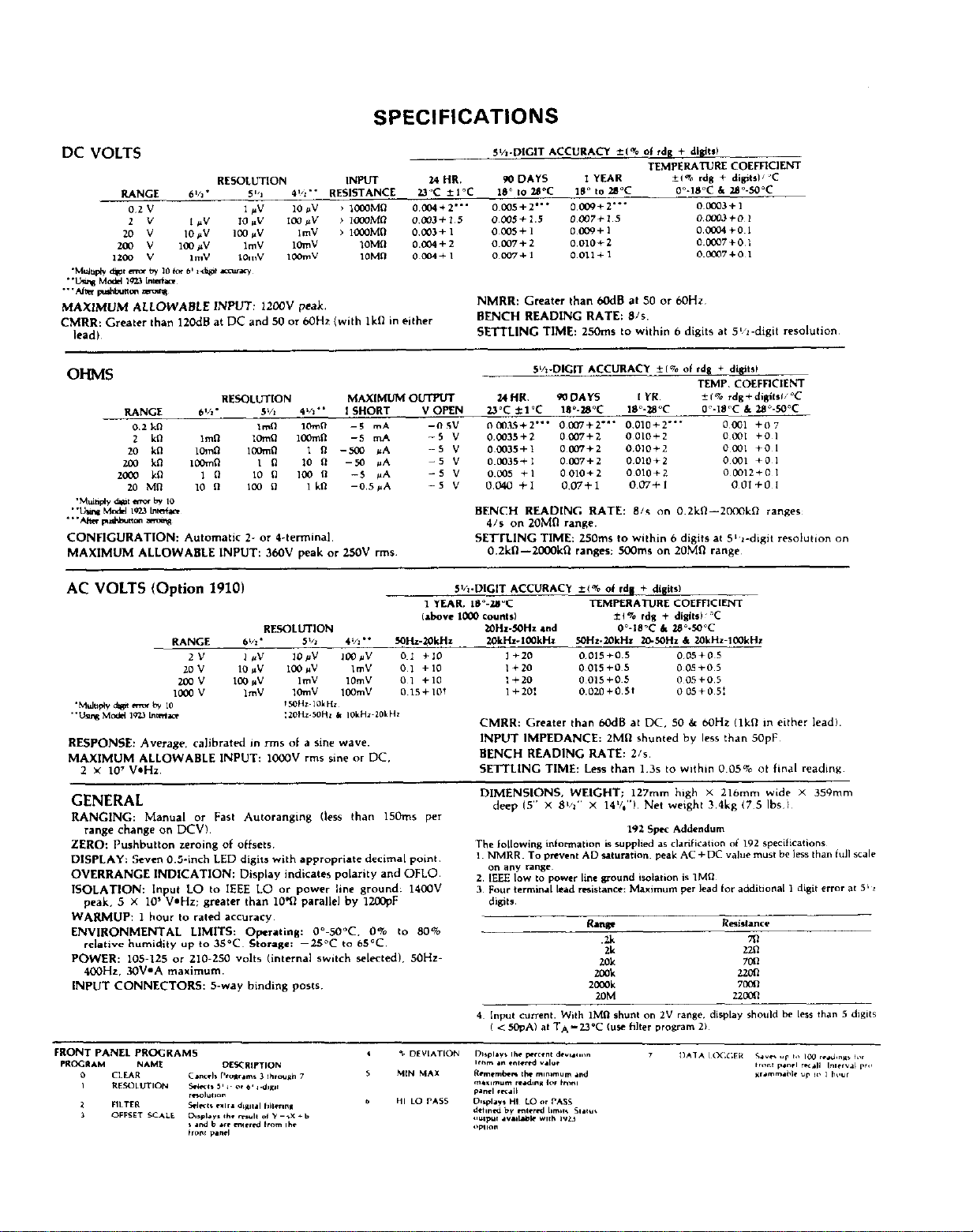
DC
SPECIFICATIONS
VOLTS
Page 5
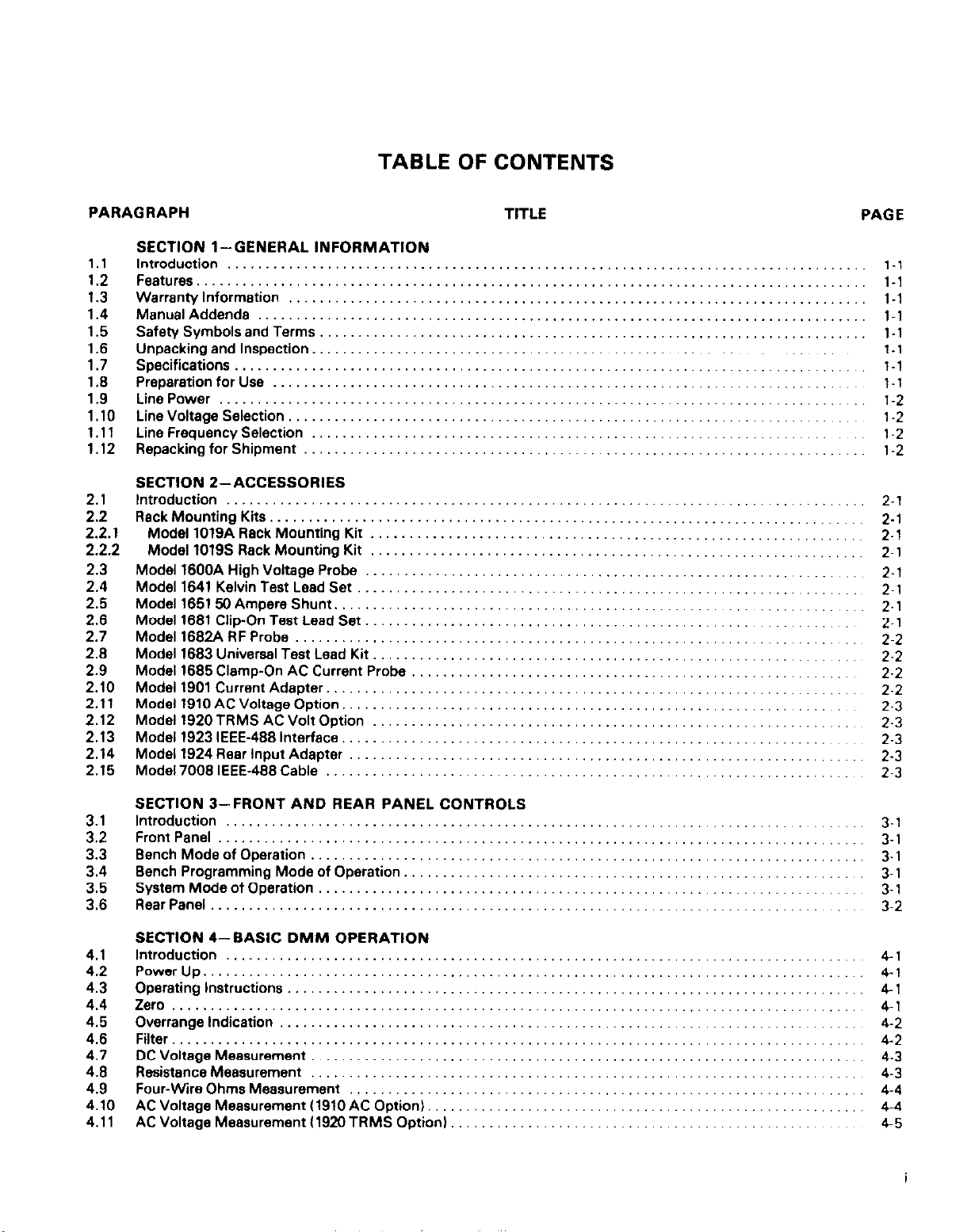
TABLE OF CONTENTS
PARAGRAPH TITLE PAGE
1.1
1.2
1.3
1.4
1.5
1.6
1.7
1.8
1.9
1.10
1.11
1.12
2.1
2.2
2.2.1
2.2.2
2.3
2.4
2.5
2.6
2.7
2.8
2.9
2.10
2.11
2.12
2.13
2.14
2.15
SECTION l-GENERAL INFORMATION
Introduction ...................................................................................
Features .......................................................................................
WarrantyInformation
ManualAddenda
SafetySymbolsandTerms
Unpackingandlnspection
Specifications.
Preparation for Use
Line Power
Line Voltage Selection
LineFrequencySelection
Repackingforshipment
SECTION Z-ACCESSORIES
Introduction
RackMountingKits
Model1019ARackMountingKit
Model1019SRackMountingKit
Model1600AHighVoltageProbe
Model1641KelvinTestLeadSet..............................................................~~
Model165150AmpereShunt................................................................~
Model1681Clip-OnTestLeadSet.............................................................~
Model1682ARFProbe......................................................................~
Model 1683 Universal Test Lead Kit. ..........................................................
Model 1685 Clamp-On AC Current Probe
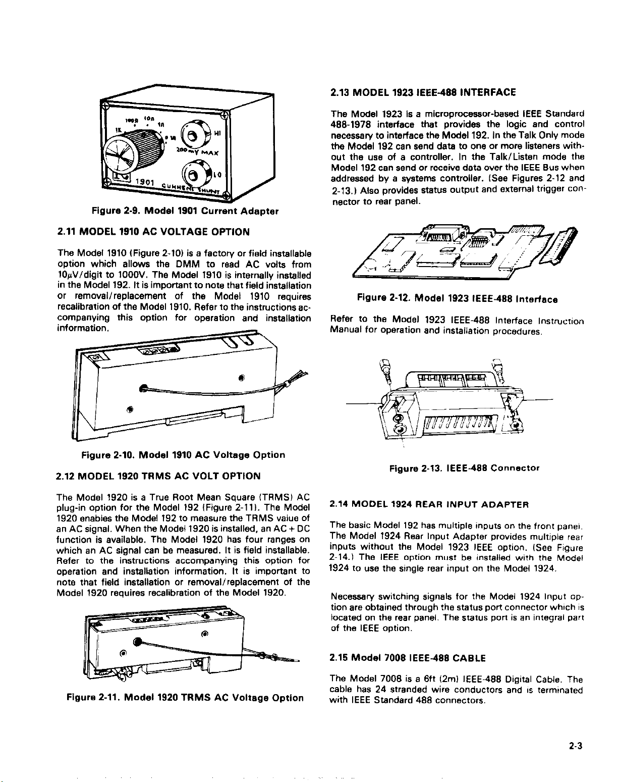
Model1901CurrentAdapter ......................................................................
Model1910ACVoltageOption...............................................................~
Model1920TRMSACVoltOption
Model19231EEE-488lnterface...............................................................~~~~
Modal1924RearlnputAdapter..............................................................~.~~
Model7008IEEE.488Cable..
....................................................................................
...................................................................................
...........................................................................
...............................................................................
.......................................................................
........................................................................
................................................................................
............................................................................
..........................................................................
...................................................................
.........................................................................
.............................................................................
................................................................
................................................................
.................................................................
........................................................
................................................................
..................................................................
.~,~
...
...
..
..
1-l
l-l
l-l
1-l
l-l
l-l
l-l
l-l
1-2
l-2
1.2
1-2
2-l
2-1
2-l
2-1
2-l
2-1
2-l
2-l
2-2
2-2
2-2
2-2
2~3
2-3
2-3
2-3
2-3
3.1
3.2
4.1
4.2
4.3
4.4
4.5
4.6
4.7
4.8
4.9
4.10
4.11
SECTION 3-FRONT AND REAR PANEL CONTROLS
Introduction
Front Panel
BenchModeofOperation
Bench Programming Mode of Operation.
SystemModeofOperation
RearPanel
SECTION 4-BASIC DMM OPERATION
Introduction
Powerup....................................................................................~
Operating Instructions
zero .........................................................................................
Overrangelndication
Filter .........................................................................................
DCVoltageMeasurement
ResistanceMeasurement
Four-Wire Ohms Measurement ...................................................................
AC Voltage Measurement (1910AC Option).
AC Voltage Measurement l192OTRMS Optionl,
...................................................................................
....................................................................................
........................................................................
.........................................................
.......................................................................
.....................................................................................
...................................................................................
...........................................................................
............................................................................
........................................................................
......................................................................
........................................................
....................................................
3-1
3-l
3-l
3-l
3-l
3-2
4-l
4-1
4-l
4-l
4-2
4-2
4-3
.,
4-3
4-4
4-4
45
Page 6
TABLE OF CONTENTS (CONT.1
PARAGRAPH
SECTION ‘&FRONT PANEL PROGRAMS
5.1
5.2
5.3
5.4
5.5
5.6
5.7
5.8
Introduction
.................................................................................................................................................................... Program Notes
P,og,a,“OC,~~, ................................................................................
Programl.Resolution
ProgramZ.Filter
Program3.Dffset/Scale
Program4. Percent Deviation.. ...................................................................
Program5,Min/Max
5.9
;:;(: Program7.DataLogger
5.12 ProgramB.ServiceProgram
6.1
6.2
Program&HI/LO/PASS
lEEEBufferOpmt,on
SECTION 6-PERFORMANCE VERIFICATION
Introduction ...................................................................................
Environmental Conditions ........................................................................
6.3
6.4
6.5
6.5.1
6.5.2
6.5.3
6.5.4
7.1
7.2
7.3
7.3.1
7.3.2
7.3.3
RecommendedTestEquipment
InitialConditions
Performanceverification
DC Voltage Accuracy Check 12OV to 12OOV ranges)
DC Voltage Accuracy Check (.2V to2V ranges1
AC Voltage Accuracy Check (With Model 1910 AC Voltage Option Installed)
Resistance(R)AccuracyCheck
SECTION 7-THEORY OF OPERATION
Introduction
Overall Functional Description
Analog Circuit Description
InputMultiplexer .............................................................................
...................................................................................
DCVoltage Measurement
ResistanceMeasurement
7.3.4 ACVoltageMeasurement
7.3.5
7.3.6
7.4
7.4.1
7.4.2
7.4.3
7.4.4
7.4.5
7.4.6
7.5 AIDControl ..................................................................................
7.5.1 ClockCircuit
7.6 DisplayCircuit
7.7
InputBufferAmplifier
AIDConverter ...............................................................................
Digital and Display Circuit Description
Microcomputer (Refer to Schematic 309750)
Memon/
AddressDecoder..
Reset ......................................................................................
FrontPanelSwitchPort
LineFrequency
PowerSupply
..............................................................................................................................................................
...........................................................................
.........................................................................................................................................................
............................................................................
.................................................................................................................................................
...........................................................................
......................................................................
...................................................................................................................................................
.........................................................................
.................................................................
....................................................................
.......................................................................
............................................................................................................................................
...............................................................................................................................................
..............................................................
.......................................................................
..............................................................................
.................................................................................................................................................................
.................................................................................
TITLE
.............................................
.................................................
.....................................................
...........................
PAGE
5-1
5.,
;I;
5-4
5-4
z:E
5-J
5-B
;I;
E:;
E:i
..
;:;;
;:;;
7.11
7.11
;I;:
7.14
6-l
6-l
;I:
6-2
7-l
7~1
7-3
7-3
;:;
;I:
7-7
;:;
SECTION E-MAINTENANCE
6.1 Introduction ...................................................................................
6.2 Calibration
6.2.1 RecommendedTestEquipment
8.2.2 Environmental Conditions
ii
.....................................................................................
.................................................................
...................................................................... B-1
B-l
8.1
B-l
Page 7
TABLE OF CONTENTS (CONT.)
PARAGRAPH
8.2.3
8.2.4
8.3
8.3.1
8.3.2
8.3.3
8.3.4
8.4
8.4.1
8.4.2
8.4.3
8.4.4
8.4.5
9.1
9.2
9.3
9.4
9.5
Warmup ................................................
Calibration Adjustments ...................................
Troubleshooting Set-Up Procedures
Line Power Fuse iFlO1) Replacement
Line Voltage Selection .....................................
Disassembly .............................................
Special Handling of Static Sensitive Devices
Troubleshooting Procedure ...................................
Line Power ..............................................
A/D Converter and Display .................................
ACConverter ............................................
DC Attenuator and Ohms Sources and Resistors.
DigitalBoard
SECTION B-REPLACEABLE PARTS
lntrodution ................................................
Parts List ..................................................
Ordering Information ........................................
Factory Service
Schematic Diagrams and Component Location Drawings
...........................
........................
.............................................
.............................................
TITLE
..................
..............
.........
.....................
......................
......................
......................
.... .... ..... ......
......
......
......
......
......
......
......
PAGE
8-l
ai
8-2
8-2
8-4
8.4
8-5
8-5
8-6
8-6
86
86
86
9-1
9-1
9-1
9-l
9- 1
iii
Page 8
LIST OF ILLUSTRATIONS
FIGURE
l-l
2-1
2-2
2-3
2-4
2-5
2-6
2-7
2-8
2-9
2-10
2.11
2-12
2-13
2.14
3-l
3-2
4-1
4-2
4-3
4-4
4-5
4-6
5-1
6-l
7~1
7-2
7-3
J-4
7-5
7-6
J-7
J-8
7-9
7-10
7-11
7-12
7.13
7-14
7.15
7-16
7.Ii
J-18
7-19
7-20
8-l
9-1
9-2
9-3
9-4
9-5
TITLE
Instrument Packaging
Model1019RackMountingKit ....................................................................
Model1600AHighVoltageProbe
Model 1641 Kelvin Test Lead Set
Model165150AmpereShunt
Model1681Clip-OnTestLeadSet
Model1682ARFProbe..........................................................~......~ ........
Model 1683 Universal Test Lead Kit
Clamp-OnACCurrentProbe ......................................................................
Model1901CurrentAdapter.............................................................~ ........
Model1910ACVoltageOption ....................................................................
Model 1920 TRMS AC Voltage Option
Model 1923 IEEE-488 Interface
IEEE-488Connector....................................................................~..~ .....
Model1924RearlnputAdapter
Modell92FrontPanel.............................~.............................~.~ .............
Model192RearPanel
Effect of Zero Function on Dynamic Range of Measurements
InputFilterFiesponseGraph
DCVoltageMeasurements
ResistanceMsasurements................~..........................~............~......~...~
Four-Wire Resistance Measurement
ACVoltage Measurements
Front Panel Program Buttons
TestCircuit,2mVand2V............~
Basic Block Diagram
Simplified Multiplexer Schematic.
DCVoltage Measurement
FET Switching Sequence for DC Voltage Measurement (Bench Mode of Operation)
DC Voltage Measurement FET Switching Sequence (System Mode of Operation1
Resistance Measurement Simplified Circuit
FETSwitchingSequenceforOhmsMeasurement
Affect of Lead Resistance in 2.Terminal Ohms Measurements.
Affect of Lead Resistance in 4.Terminal Ohms Measurements.
Block Diagram AC Volts Operation
ACVoltsOperationFlowChart..~ ....................................
Simplified Input Buffer Schematic
Simplified A/D Converter Schematic
AID Converter Integrator Output Waveform
Microcomputer Block Diagram
ChargeBalanceTimming
SingleSlopePhase.........~.........................................................~ ........
Simplified Schematic of Latch
Simplified Oscillator/Divider Diagram
Display Schematic
Adjustment Locations
Exploded View With Mechanical Parts
AC Converter, Component Location Drawing
MotherBoard,ComponentLocationDrawing
Analog Board, Component Location Drawing
Display Board, Component Location Drawing
...........................................................................
.................................................................
..................................................................
....................................................................
.................................................................
................................................................
.............................................................
..................................................... .....
.................................................................
..........................................................................
......................................................................
.....................................................................
.............................................. ..
........................................................... ~, ...
.................
.........................................................
.................................................................... ,.,
.................................. ...........
....................................................
......
..............
.............
..................................................................
.....................................................................
.............................................................. ....
..................................
.................................................................
..............................................
.............................................................
.................... ....... ..
....... ~,
................................
............... ...
.....
.....................
.......
......................................................
......................................................
......................................................
......................................................
....................... ................
.. ...... .. ..
.....
..................
................ ..
.......................... .... .. ....
...................... ...
....................................
...... ....
..........
~,.,~
......
..........................
.................
..
.....
., ., .....
.. .. .. .. ..
~.~.~,,
.. .... ..... ....
.....
.....
... ..
...........
..........
...
..
PAGE
l-2
2-1
2-l
2-1
2-1
2-2
2-2
2-2
2~2
2-3
2-3
2~3
2-3
2~3
2-J
3~:~
3-2
4~’
4~2
4~3
44
4~i
4~4
52
6-2
7~1
7~2
7~3
7-4
7~4
7~5
‘~6
M
7Yz
J-7
7~8
7-9
7-9
7.10
7~12
7~:3
7-14
7-15
7-15
7-16
8-3
9-2
9.11
9-13
9-17
9-21
iv
Page 9
LIST OF ILLUSTRATIONS (CONT.)
FIGURE
9-6
9-7 MotharBoard.SchematicDiagram............................................................... 9.25
9-a
9-9
AC Converter, Schematic Diagram g-23
Analog Board, Schematic Diagram
Display Board, Schematic Diagram
TITLE
PAGE
g-29
g-33
LIST OF TABLES
TABLE
4-l
4-2
4-3
4-4
5-l
52
6-l
6-Z
6-3
6-4
6-5
7-1
7-2
7-3
7-4
6-l
6-2
8-3
9-4
86
6-5
a-7
a8
a-9
a10
6-11
6-12
El3
6-14
9-1
9-2
9-3
9-4
9-5
TITLE
LineVoltagaSalection
MaximumInput
ResistanceRanges .............................................................................
Maximum Four-Wire Test Lead Resistance.
FrontPanalProgramSummary
Data Point Times
Recommended Test Equipment for Performance Verification
DC Voltage Performance Check (2OV to 12OOV Rangel
ACVoltageAccuracyChack
ZeroReading ..................................................................................
ResistanceAccuracyChack .....................................................................
SenlingDelays.SNontoTurnonoflntegrator..
MamoryByteLocations...............................................................~..~
FunctionsofLatchOutputs ....................................................................
Power Supply Component Identification.
Recommended Test Equipment for Calibration
CalibrationProcaduras.................................................................~~~
Fuse Replacement .............................................................................
LineVoltagaSalaction................................................................~~~~
TestNumberSummarization .....................................................................
Static Sensitive Devices .........................................................................
Program 8 A/D Test-FET Switching Sequence
LinePowarChecks................................................................~...~
AIDConvarterChacks .....................................................................
Display Checks..
ACConvartarCheckslModel1910) ................................................................
DCAnanuatorChacks.....................................................................~
Ohms Source and Resistors Checks. ..............................................................
DigitalBoardChecks....................................................................~..~.~
Modal192DrawingPackage..............................................................~..~..~
AC Converter PC-496, Parts List
MotharBoardPC-559,PartsList........................................................~~
Analog Board PC-560. PartsList
Display Board PC-530, Parts List
...........................................................................
...............................................................................
............................................ .....
...................................................................
..................................................................
...................................... ..
......................................... ..
..................................................................... 62
.........................................
.............................................. .....
....................................................
......................................... .......
.............................................................................
............................................................
............................................................
................................................................
....... 5-9
........
.......
......
PAGE
....
......
.....
...
.~~ 6.6
.... 6.10
.....
..
4-l
4-1
4-3
4-4
5-l
6-l
6-2
6-3
6-3
7-8
7-10
7-13
7-15
6-l
a-2
6-4
6-4
6-6
8-5
6.7
a-a
6.9
6.9
9-l 1
6-11
9-1
9-3
9.4
9.6
9-9
v/vi
Page 10

Page 11
SECTION 1
GENERAL INFORMATION
1.1 INTRODUCTION
This instruction manual contains complete operating in-
structions for the Keithley Model 192. Detailed descriptions
of the available options for the Model 192 are provided
lseperate instruction manuals are supplied with the Model
1920 and Model 19231, along with a theory of operation,
calibration and service instructions for maintaining the instrument. A complete parts list with schematics and component layouts is also provided at the end of this manual.
The Model 192 is a 6’h digit, 2,000,OOO count, fast
autoranging DMM. With the IEEE-468 interface option
(Model 1923). the Model 192 becomes fully programmable.
DC Volts and Ohms functions are standard. Measurements
of l&V to 12OOV are attainable on 5 voltage ranges, and
Z-and 4-terminal messurements of 1mD to ZOMR are attainable on 6 resistance ranges. With the addition of the
Model 1910 AC Voltage Option, the Model 192 will provide
readings from 1OrV to 1OOOVAC on 4 ranges. True Root
Mean Square ITRMS) AC voltages can also be attained with
the use of the Model 1920 TRMS ACV Option. Because the
Models 1910, 1920, and 1923 are easily field installed, these
options can be added at any time.
1.2 FEATURES
The Model 192 includes the following features:
Front Panel Programs-The internal programs in the
Model 192 are accessible from the front panel. Descriptions of these programs can be found in the detailed specifications which precede this Section and in Section 5.
Data Storage- Registers for storing 100 readings are provided in the basic Model 192. These storage registers are
utilized by Front Panel Program 7. Data Logger (see
Section 51.
Multiple Inputs-Multiple inputs provide access to DCV.
ACV, and Ohms terminals simultaneously. This enables
systems designers to optimize their switching matricies
for the parameter being measured. In addition, in some
simple systems, switching can be eliminated altogether.
For systems that require only one input, the Model 1924
Rear Panel Input Adapter is available as an option.
One Button Zero-The front panel zero is activated by
pushing one button. The zero offset is automatically scaled when a new range is selected. Unique offset settings
are saved for each function.
the proper action to be taken. Keithley maintains service
facilities in the United States, West Germany, Greet Britain,
France, the Netherlands, Switzerland, and Austria. Information concerning the application, operation or service of your
instrument may be directed to the applications Engineer at
any of the above locations. Check the inside Front Cover of
this manual for addresses.
1.4 MANUAL ADDENDA
Improvements or changes to this manual will be explained
on an addemdum attached to the inside back cover.
1.5 SAFEN SYMBOLS AND TERMS
Safety symbols used are as follows:
The symbol
A
on the instrument denotes that
the user should refer to the operating instructions.
The symbol
i,
on the instrument denotes that
1OOOV or more may be present on the terminal(sl.
The WARNING used in this manual explains dangers that
could result in personal injuy or death.
The CAUTION used in this manual explains hazards that
could damage the instrument.
1.6 UNPACKIrdG AND INSPECTION
The Model 192 was carefully inspected both mechanically
and electrically before shipment. Upon receiving the Model
192, unpack all items from the shipping container and check
for any obvious damage that may have occurred during
transit. Report any damage to the shipping agent. Retain
and use the original packaging materials if reshipment is
necessan/. The following items are shipped with all Model
192 orders:
l
Model 192 Programmable DMM
l
A Model 192 instruction Manual
l
Installed or separate optional accessories, as ordered
1.7 SPECIFICATIONS
For Model 192 detailed specifications, refer to the specifications that precede this section.
1.3 WARRANTY INFORMATION
Warranty information is given on the inside front cover of
this manual. If there is a need to exercise the warranty, contact the Keithley representative in your area to determine
1.8 PREPARATION FOR USE
The Model 192 is shipped ready for use on the line voltage
marked on its rear panel. The line frequency 150 to 400Hzl is
selected automatically by the Model 192 during power up. If
l-l
Page 12
the Model 1923 IEEE Interface is installed it will be set to the
Addressable mode and et Address 8.
1.9 LINE POWER
The Model 192 is provided with a J-wire line cord which
mates with a third wire earth grounded receptacle. The instrument will operate on two of four voltage ranges listed in
Table B-4. These ranges may be selected by positioning an
internal slide switch and installing the appropriate fuse for
that range. An optional line voltage range of SO to 110 volts
is available by special order. Instruments with this range use
a different transformer.
1.10 LINE VOLTAGE SELECTION
Refer to Section 6 Maintenance to select the proper line
voltage settings.
CARDBOARD STRIP
NSTRUCTION MANUAL
1.11 LINE FREQUENCY SELECTION
Line frequency is sensed automatically by the Model 192
during power up. The instrument will operate at 50 to 400Hz
end will display F60 at 60Hz or F50 at either 50Hz or 400Hz.
1.12 REPACKING FOR SHIPMENT
The Model 192 should be packed in its original carton using
the packaging method shown in Figure l-l. Before packag-
ing, wrap the instrument in plastic. After it is placed in the
box, surround the instrument with styrofoam packaging
material.
If the Modal 192 is to be returned to Keithley Instruments for
calibration or rapair, include the following:
l
AlTENTION REPAIR DEPARTMENT on the address label
l
Warranty status of the instrument
l
Completed service form
MODEL 192
PROTECTIVE
CARDBOARD
BOTTOM
ARDBOARD STRlP
1-2
PACKAGING MATERIAL
L
1
Figure l-l. Instrument Packaging
Page 13
SECTION 2
ACCESSORIES
2.1 INTRODUCTION
This section describes the various accessories and options
available for use with the Model 192 OMM.
2.2 RACK MOUNTING KITS
2.2.1 Model 1019A Rack Mounting Kit
The Model 1019A is a universal rack mounting kit for the
Model 192. Two different front panels &we provided to allow
left, right, or dual Iside-by-side) installation. ISee Figure
2-1.1
Figure 2-2. Model 16OOA High Voltage Probe
2.4 MODEL 1641 KELVIN TEST LEAD SR
The Model 1641 test leads (Figure 2.3) are used in making
4-terminal measurements. The test leads I1 pair1 are twin-
lead cables 1.2m 146 inches1 long. Each cable is terminated
by a twin-banana plug and a spring-clip Kelvin contact. Plug
the twin banana plugs into the DMM horizontallv (HI to HI
and LO to LO).
Figure 2-1. Model 1019 Rack Mounting Kit
2.2.2 Model 1019s Rack Mounting Kit
Model 1019s slide rack mounting kit enables one or two half
rack size instruments to be rack mounted with the added
feature of sliding the instrumentls) for easy access. The
dimensions are 133mm x 463mm (5% x 19 inl.
2.3 MODEL WOOA HIGH VOLTAGE PROBE
The Model 1600A (Figure 2-2) extends the DMM measure-
ment capabilities to 40kV. It has a 1M)O:l division ratio I1
lolt on the DMM corresponds to 1 kilovolt).
Figure 2-3. Model 1641 Kelvin Test Lead Set
2.6 MODEL 1661 66 AMPERE SHUNT
The Model 1651 (Figure 2-4) allows current measurements
to be made from 0 to 50 amperes DC and up to 50 amperes
AC with AC Voltage option. It is a 0.001 ohm + 1%
4-terminal shunt. A 50 ampere current will correspond to
50mV.
Figure 24. Model 1661 M Ampere Shunt
2.6 MODEL 1681 CLIP-ON TEST LEA0 SET
The Model 1661 (Figure 2-6) contains two leads 1.2117 146in. I
long, terminated with banana plug and spring-action clip-on
probe.
2-l
Page 14
Figure 2-7. Model 1663 Universal Test Lead Kit
Figure 2-6. Model 1661 Clip-On Test Lead Set
2.7 Model 1682A RF Probe
The Model 1662A is en RF probe that permits measure-
ments of AC voltages at frequencies from 1OOkHz to
250kHz. Connect the probe to the input terminals of the
DMM. Select the DCV function and the appropriate range.
The Model 1662A will give en output of one volt for an input
of one volt rms when usad with instruments having an input
impedance of 10MlI. ISee figure 2-6.)
Figure 2-6. Model 1662A RF Probe
2.6 MODEL 1663 UNIVERSAL TEST LEA0 KIT
The Model 1663 consists of two test leads 1.2m (48in. l long
with 12 screw-in tips, 2 banana plugs, 2 spade lugs, 2
alligator clips with boots, 2 needle tips with chucks, and 4
heavy-duty tip plugs. (See Figure 2-7.)
2.9 MODEL 1666 CLAMP-ON AC CURRENT PROBE
The Model 1666 (Figure 2-8) measures 60Hz and 60Hz AC
current by clamping onto a single conductor. Interruption of
the current path is unnecessary. The Model 1685 detects
current by sensing magnetic field produced by current.
Figure 24. Clamp-On AC Current Probe
2.10 MODEL 1901 CURRENT ADAPTER
The Model 1901 (Figure 2-91 allows the DMM to read DC
current from lnA/digit to 2000mA. With the Modal 1910
AC voltage option it reads from lOnA/digit to 2000mA. The
Model 1901 plugs into the INPUT terminals of the Model
192. Maximum allowable continuous voltage drop (full scale
input voltage burden) is 200mV. Shunt resistors are connected to eliminate contact resistance errors. Use the Model
192 200mVDC range and 2VAC range for DC current and
AC current respectively. Input voltage burden can be reduc-
ed by selecting the lowest shunt that provides the necessary
resolution.
2-2
Page 15
2.11 MODEL 1910 AC VOLTAGE OPTION
The Model 1910 (Figure 2-10) is a factory or field installable
option which allows the DMM to read AC volts from
lO@/digit to 1OOOV. The Model 1910 is internally installed
in the Modal 192. It is important to note that field installation
or removal/replacement of the Modal 1910 requires
recalibration of the Model 1910. Refer to the instructions ac-
information.
2.13 MODEL 1923 IEEE-466 INTERFACE
The Model 1923 is a microprocessor-based IEEE Standard
466-1976 interface that provides the logic and control
necessary to interface the Model 192. In the Talk Only mode
the Model 192 can send data to one or more listeners with-
out the use of a controller. In the Talk/Listen mode the
Model 192 can send or receive data over the IEEE Bus when
addressed by a systems controller. (See Figures 2-12 and
2-13.) Also provides status output and external trigger con
nector to rear panel.
Figure 2-12. Model 1923 IEEE-466 lnterfsce
Refer to the Model 1923 IEEE-468 Interface Instruction
Manual for operation and installation procedures.
Figure 2-10. Model 1910 AC Voltage Option
2.12 MODEL 1920 TRMS AC VOLT OPTION
The Model 1920 is a True Root Mean Square ITRMSI AC
plug-in option for the Model 192 (Figure Z-11). The Model
1920 enables the Model 192 to measure the TRMS value of
an AC signal. When the Model 1920 is installed, an AC + DC
function is available. The Model 1920 has four ranges on
which an AC signal can be measured. It is field installable.
Refer to the instructions accompanying this option for
operation and installation information. It is important to
note that field installation or removal/replacement of the
Model 1920 requires recalibration of the Model 1920.
Figure 2-11. Model 1920 TRMS AC Voltage Option
Figure 2-13. IEEE-466 Connector
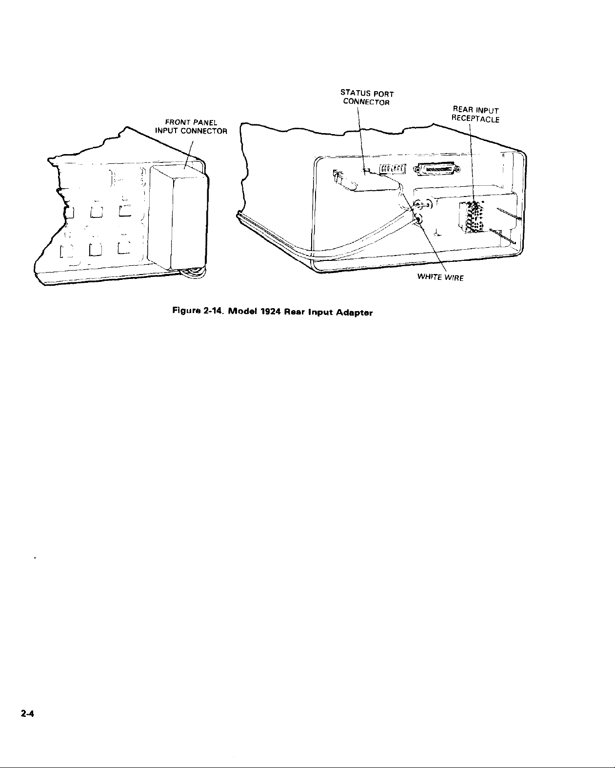
2.14 MODEL 1924 REAR INPUT ADAPTER
The basic Model 192 has multiple inputs on the front panel.
The Model 1924 Rear Input Adapter provides multiple rear
inputs without the Model 1923 IEEE option. (See Figure
2-14.1 The IEEE option must be installed with the Model
1924 to use the single rear input on the Model 1924.
Necessav switching signals for the Model 1924 Input op-
tion are obtained through the status port connector which is
located on the rear panel. The status port is an integral part
of the IEEE ootion.
2.15 Model 7008 IEEE-466 CABLE
The Model 7008 is a 6ft l2m) IEEE-488 Digits Cable. The
cable has 24 stranded wire conductors and is terminated
with IEEE Standard 488 connectors.
2-3
Page 16
FRONT PANEL
INPUT CONNECTOR
Figure Z-14. Model 1924 Rear Input Adapter
STATUSPORT
CONNECTOR
WHITE W,RE
2-4
Page 17
SECTION 3
FRONT AND REAR PANEL CONTROLS
3.1 INTRODUCTION
This section describes the Model 192 front and rear panel
controls. Refer to Figures 3-1 and 3-2.
3.2 FRONT PANEL
The Front panel features are explained under the following
modes of operation:
l
Bench Mode of Operation
l
Bench Programming Mode of Operation
l
System Mode of Operation
3.3 BENCH MODE OF OPERATION
Power ON/OFF Button-Power is ON with button IN;
power is OFF with button OUT.
Display-Display is direct reading in AC and DC volts. Ohms
is read in kfl, except the 20MR range which is read in
megohms. 5’h digits of resolution is standard in the Bench
mode.
IEEE-488 Bus Indicator-The indicators (Talk, Listen and
Remote1 are used during remote operation of the Model
192. They can be disregarded during the Bench mode of
operation.
Input Terminals-There are separate connections for DCV,
ACV, and Ohms with the use of five-way binding posts.
Range Push Buttons-These seven momentary switches
are used to select range. The annunciators indicate which
range the instrument is in, and if it is in Manual or Auto
ranging.
Function Push Buttons-These three push buttons select
either DCV, ACV lif the option is installed), or kR.
Zero Push Buttons-This button controls the internal Zero
program (See paragraph 4-41. An illuminated annunciator
indicates Zero function is enabled.
Programming Push Buttons-These two momentary switches are used during tha Bench Programming mode of
operation. They can be disregarded during the Bench mode.
Tilt Bail-The tilt bail is used as a handle and also to elevate
the front of the instrument for better Viewing.
3.4 BENCH PROGRAMMING MODE OF OPERATION
Display-The utilization of Front Panel PROGRAM 1 increases resolution to 6% digits (see paragraph 5.41.
IEEE-466 Bus Indicator-The indicators (Talk, Listen and
Remote) are used during remote operation of the Model
192. They can be disregarded during the Bench mode of
operation.
Input Terminals-There are separate connections for DCV.
ACV, and Ohms with the use of five-way bindinq posts.
PROGRAM $ through PROGRAM 5-The number 0
.through 5 and the sign I-l to the left of the Range push buttons are used to select their corresponding programs or
enter data.
PROGRAM 7 through PROGRAM g--The number 7,8. and
9 at the left of the Function push buttons are “sed to select
their corresponding program or enter data,
PROGRAM 6-The number 6 at the left of the Zero push
button is used to select front panel PROGRAM 6 or enter
data.
Programming Push Buttons-PRGM-This button enables
the selection of front panel programs. RECALL-This butt
ton has three function levels or uses. The first function level
(RECALL) displays the currant program along with data, if
any. The second function level (ENTI is used to enter programming data. The third function level is a trigger for the
System mode.
3.5 SYSTEM MODE OF OPERATION
Power ON/OFF Switch-Power is ON with button IN;
power is OFF with button OUT.
Display-In the System mode, the Model 192’s resolution is
determined by the conversion rata. Refer to IEEE-469 Bus
Operator Manual.
IEEE-466 Bus Indicator-These indicators (Talk. Listen and
Remote) identify the present status of the IEEE Bus.
Input Terminal-There are separate connections for DCV.
ACV, and Ohms with the use of five-way binding posts.
Range Push Buttons-These seven momentary switches
are used to select range. The annunciators indicate which
range the instrument is in, and if it is in Manual or Auto
Range.
Power ON/OFF Button-Power is ON with button IN:
power is OFF with button OUT.
Function Push Buttons-These three push buttons select
either DCV, ACV lif the option is installed), or k0.
3-1
Page 18
Zero Push Buttons-This button controls the internal Zero
program ISee paragraph 4.4). An illuminated annunciator
indicates Zero function is enabled.
3.6 REAR PANEL
The following information describes Model 192 rear panel
controls.
Power Connector-The instrument will operate on four
voltage ranges of 50 to 400Hz AC power Isee paragraph 1.9
and 1.10).
Fuse-See paragraph 8.5.1 for the proper fuse replacement.
Status Output’ and External Trigger-Six active low out-
puts and the external trigger input are available through the
Status Output Connector. Three of the outputs are funtion
(ACV, DCV, kR). The remaining outputs are PASS, LOW,
HIGH which are used with the internal program
HI/LO/PASS. The function outputs are continuously
active, the PASS, LOW, HIGH outputs are active only when
utilizing the HI/LO/PASS program. The external trigger requires a 0 to 5V logic signal and is recognized only when in
system mode.
IEEE-488 Interface Connector’-This is the IEEE-488 con“action to the Modal 192.
Address Switches*-These switches are used to set up the
Model 1923 IEEE-488 interface.
Accessory Mounting Holes-These are threaded mounting
holes for the rear input adapter,
l
These functions are present when the Model 1923 option
is installed.
\ - \‘IWU. 1m1*..
.
1 /
Figure 3-1. Model 192 Front panel
Figure 3-2. Model 192 Rear Panel
I”“*Y) i-
,i
\
1
3-2
Page 19
SECTION 4
BASIC DMM OPERATION
4.1 INTRODUCTION
This section contains procedures for connecting and
operating the Model 192.
4.2 POWER UP
Plug the instrument into the proper power receptacle in ac-
cordance with Table 4-l.
Table 4-l. Line Voltage Selection
Input
Voltage
105-125VAC
210-250VAC 230VAC
90-IlOVAC’ 115VAC
195235VAC’ 230VAC
‘For instruments equipped with a low voltage transformer,
lmmediatley after turning on the Model 192 via the POWER
switch, the Display will indicate the following:
1. This is a display test. The operator can note inoperative
display segments by comparing the Model 192’s display
with the figure above.
2. In addition, the push button and GPIB annunciators will
illuminate. All annunciators will illuminate simultaneously
if operating correctly.
After the display test is completed the Model 192 will display
the integration period and software level. For example;
when the following is displayed:
1. The Model 192 senses the power line frequency and sets
the A/D conversion rate.
2. The F60 indicates that the integration time has been set
for 16.6 milliseconds.
3. The C4 is a code that identifies the software revision that
is installed in the Model 192.
4. If the following is displayed the F50 indicates that the integration time has been set for 20 milliseconds.
4.3 OPERATING INSTRUCTIONS
Basic operation of the Modal 192 is presented in the following paragraphs. The upper three binding posts are used for
voltage input connections. The lower four binding posts are
used for ohms connections. The LO binding posts for
ACV, DCV and 0 are wired together.
Switch Setting
s102
115VAC
rlzKm?q
-1-6
-1-5
CAUTION
Do not apply voltages between the LO
binding posts. Instrument damage may
OCC”r.
WARNING
Maximum floating voltage is 1400VDC
or peak AC at < 5 x 10⁶V.H~. Do not exceed the maximum floating voltage
ratings. Destruction of insulation could
present e shock hazard.
The LO inputs may be floated at voltages up to 1.4kV at
5x 10⁶V*Hz. with reference to chassis ground. Chassis
ground is connected to earth ground with the line power
cord and an appropriately grounded three-wire receptacle.
WARNING
Hazardous voltages may be present on
the LO input terminals. Any voltage that
is applied to LO will also be present at
the DLO terminals.
CAUTION
Do not exceed maximum input limits
given in Table 4-2.
DC voltage sources. AC voltage sources, and Resistance
values may be connected to the input termtnals
simultaneously with consideration for possible ground loops
and noise. Refer to Table 4-2.
Table 4-2. Maximum Input
Function
4.4 ZERO
The Zero control serves as a baseline suppression subtract-
ing a stored offset or measured value from a subsequent
measurement. When the Zero control is enabled, the Zero
LED will light. All readings displayed while in the Zero mode
are the difference between the stored baseline and the
actual voltage level. The baseline obtained while the Zero
control is enabled represents a specific level or quantity of
volts or ohms. For example, if 1OOmV is zeroed. then,
1OOmVDC represents the specific level of the Zero baseline.
One hundred millovolts will then be automatically sub-
tracted from readings on any DCV range. The value for the
[ Ranga
Maximum Input
1200VDC or Peak AC
1OOOV rms sins or DC,
2x 10’V’Hz
360V peak or 250V rms
4-l
Page 20
baseline can be as little as a few microvolts or as large as
999 volts. This capacity enables the user to zero a wide
range of voltages. For example:
4.6 OVERRANGE INDICATION
Overrange is indicated by the following display:
Displayed Push
offset Zero Input Result
Example #l 1.23000 .ooooo
Example #2 .23000 .ooooo
Note
Setting range lower than the zero baseline
value, will overrange display.
WARNING
The voltage present on the input may be
greater than the displayed reading when
the instrument is Zeroed.
Example: 1OOV = stored baseline
lSOV=actual voltage to be
measured
SOV = displayed reading
One baseline can be stored for each of the functions (DC
Volts, AC Volts, and Ohms). For example, 20mVDC can be
stored for DC volts, 1OVAC volts and 50 can be stored for
ohms. Proceed as follows:
1. To store a zero value for DC volts, select the DC Volts
function. Press the ZERO Button. The reading on the
Model 192 display will be stored as the zero value. The
zero control can be disabled by pressing the ZERO button
again.
2. To store a zero value for AC volts, select the AC volts
function. Press the Zero button. The reading on the
Model 192 display will be stored as the zaro value. The
zero control can be disabled by pressing the ZERO button
again.
3. To store a zero value for Ohms, select the Ohms function. Press the ZERO button. The readina on the Model
192 display will be stored as the zero value. The zero con-
trol can be disabled by pressing the ZERO button again.
4. The Model 192 will retain these zero values. If the func-
tion is changed the Model 192 will recall the value of zero
that was set for that function. To replace an earlier stored
zero value, simply press the ZERO button twice. The
reading that was on the Model 192 will be stored as the
new zero value.
It is important to note that the use of zero reduces the
dynamic range of measurement. For instance, if
+ l.OOOOOVDC is the zeroed value, input voltages greater
than 2V would still overload the AID converter (200,000
counts). even though overrange would occur at approximately 100,000 counts displayed. Readings less than -lV
would cause overrange (2V less than + 1Vl because of the
maximum display reading of 199,999 counts. This reduction
in the dynamic range of the measurement is illustrated in
Figure 4-1. In DCV function, both the Displav dvnamic
range and the Input dynamic range can be &wed& and
thus, both can limit the dynamic range of the measurement.
Apply
1 .ooooo - .23000
1 .ooooo .77000
Displayed
If the overflow is negative then a minus I-) prefix will
precede the displayed OFLO.
\
Figure 4-l. Effect Of Zero Function on Dynamic Range
of Measurement
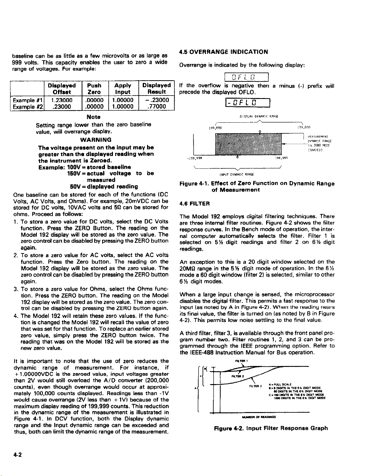
4.6 FILTER
The Model 192 employs digital filtering techniques. There
are three internal filter routines. Figure 42 shows the filter
response curves. In the Bench mode of operation, the internal computer automatically selects the filter. Filter 1 is
selected on 5’S digit readings and filter 2 on 6% digit
readings.
An exception to this is a 20 digit window selected on the
20MIl range in the 5H digit mode of operation. In the 6%
mode a 60 digit window (filter 2) is selected, similar to other
6% digit modes.
When a large input change is sensed, the microprocessor
disables the digital filter. This permits a fast response to the
input (as noted by A in Figure 4-2). When the reading nears
its final value, the filter is turned on (as noted by 6 in Figure
4.2). This permits low noise senling to the final value.
A third filter, filter 3, is available through the front panel pro-
gram number two. Filter routines 1, 2, and 3 can be programmed through the IEEE programming option. Refer to
the IEEE-466 Instruction Manual for Bus operation.
Figure 4-2. Input Filter Response Graph
9
,HPllT O”~lWC PAHW
/
4-2
Page 21
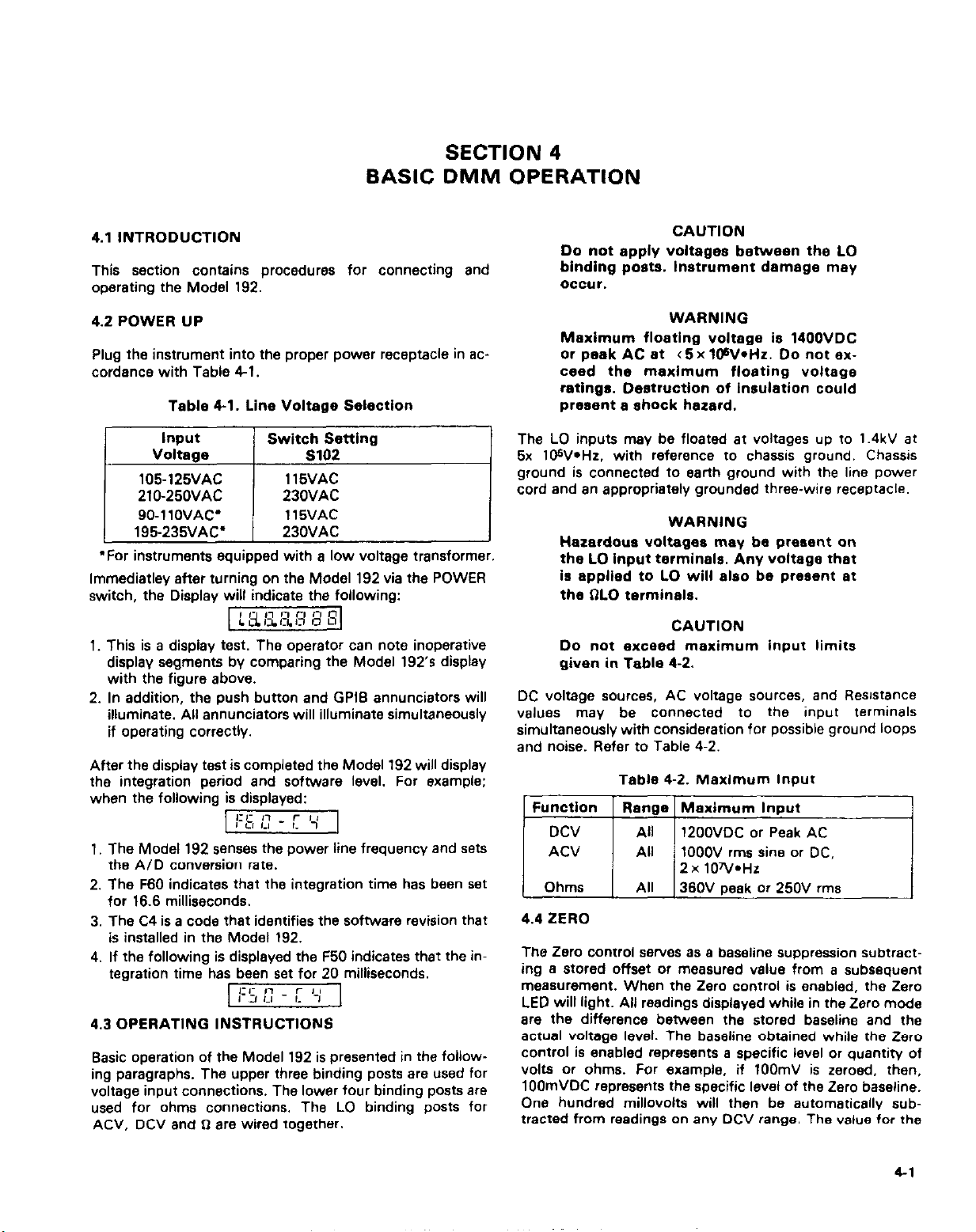
4.7 DC VOLTAGE MEASUREMENT
The Model 192 reads DC voltage from 1aV to 1200V. DC
volts are measured as follows:
CAUTION
Do not exceed the 1ZOOVDC maximum
allowable input voltage rating. Instru-
ment damage may occur.
1. Turn power ON by pressing the POWER ON/OFF button.
If the instrumc?t is within 0°C to 50°C. it is useable immediately, but a two hour warmup is required to obtain
rated accuracy.
2. Press DCV button. The Model 192 will enter the DCV
mode automatically at power up.
3. Zero instrument on the .2V range. Zero must be set with
the Zero function for rated accuracy. Zeroing is necessary
to compensate for thermal EMFs generated by the connections to the circuit to be measured. These voltages
may be only a few microwIts or several tens of
microvolts. Set Zero as follows:
A. Set the output of test circuit for zero volts or discon-
nect the test leads at the circuit and short them.
B. Set the Model 192 on the .2V range.
C. Press the ZERO button.
D. Select range from the five ranges available. The
decimal point is positioned by the Range button. The
1200V range is selected by the 2000 button. If the
20MR is inadvertently pressed when in the DCV function, the Model 192 will set the range to 1200V.
4. Connect input between the DCV and LO (see figure 43).
The binding posts accept wires, spade lugs, or banana
plugs for ease of connecting the potential to be
measured. Low thermal cabling atid connections are
recommended for measurements on the .2V range.
CAUTION
Do not exceed the 1200VDC maximum
allowable input voltage rating; Instrument damage may occur.
5. Take readings by observing the displayed digits and
decimal Point locations. All ranges are direct reading in
volts.
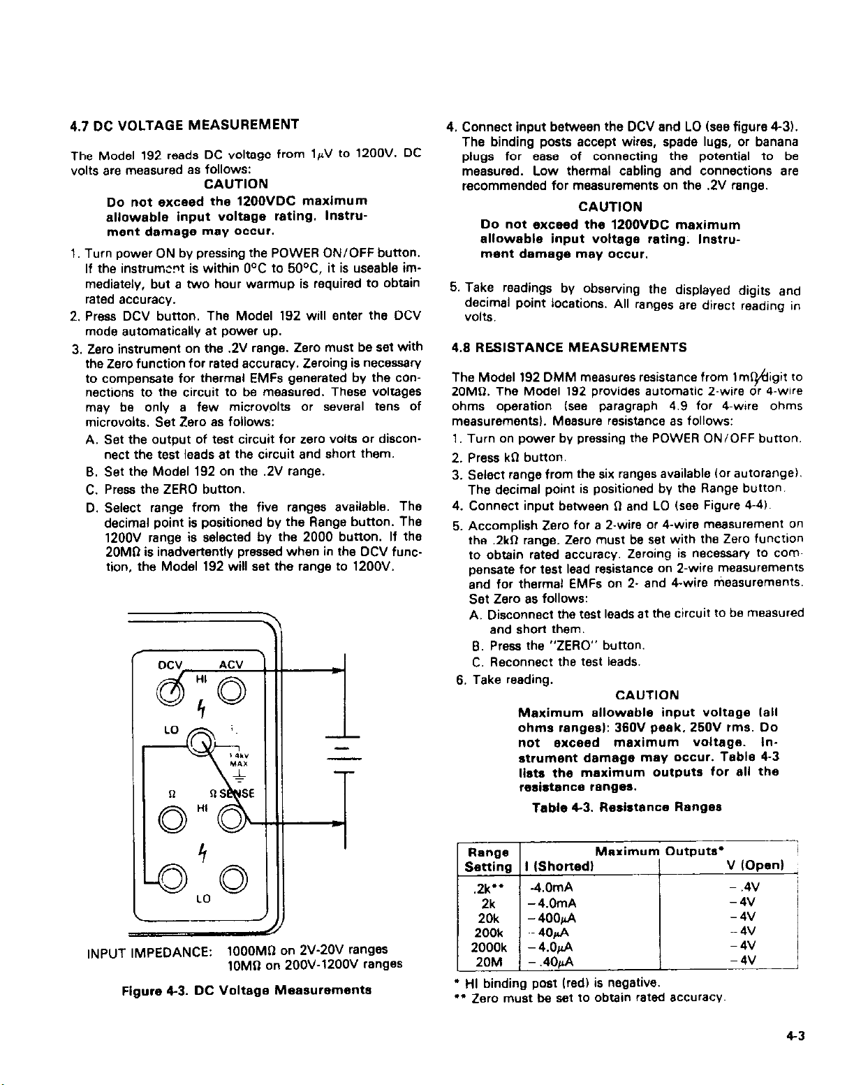
4.6 RESISTANCE MEASUREMENTS
The Model 192 DMM measures resistance from lm$figit to
20Mn. The Model 192 provides automatic 2.wire or 4.wire
ohms operation (see paragraph 4.9 for d-wire ohms
measurements). Measure resistance as follows:
1. Turn on power by pressing the POWER ON/OFF button.
2. Press kR button.
3. Select range from the six ranges available lor autorangei.
The decimal point is positioned by the Range button.
4. Connect input between n and LO Isee Figure 4-4).
5. Accomplish Zero for a 2.wire or 4.wire measurement on
the .2kQ range. Zero must be set with the Zero function
to obtain rated accuracy. Zeroing is necessav to cornpensate for test lead resistance on 2.wire measurements
and for thermal EMFs on 2. and 4.wire measurementS.
set zero as follows:
A. Disconnect the test leadsat the circuit to be measured
and short them.
B. Press the “ZERO” button.
C. Reconnect the test leads.
6. Take reading.
CAUTION
Maximum allowable input voltage lall
ohms rangesl: 38OV peek, 250V rms. Do
not exceed maximum voltage. Instrument damage may occur. Table 4-3
lists the maximum outputs for all the
resistance ranges.
Table 4-3. Resistance Ranges
INPUT IMPEDANCE:
Figure 4-3. DC
1OOOMD on 2V-20V ranges
1OMn on 2OOV-1200V ranges
Voltage Measurements
Range
Setting I (Shorted1
* HI binding post Ired) is negative.
** Zero must be set to obtain rated accuracy~
Maximum Outputs*
!
i
v IOpen) ~
4-3
Page 22
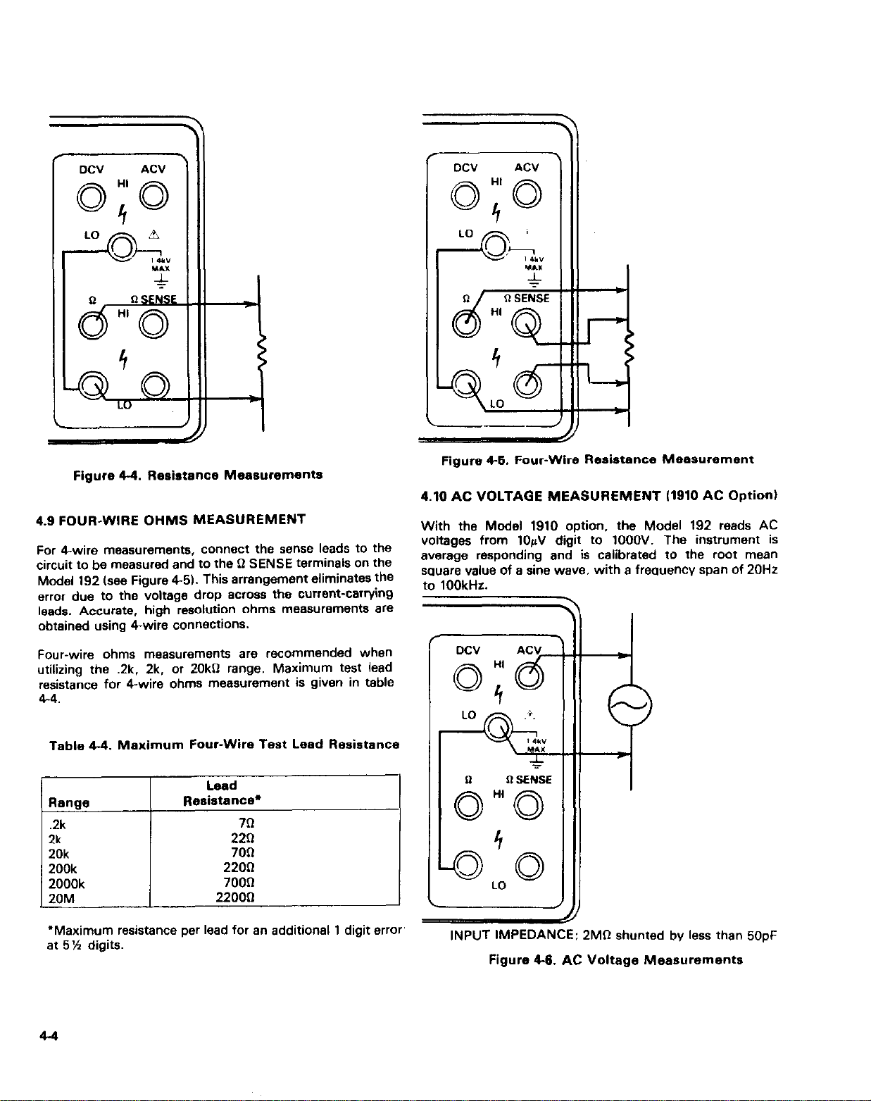
Figure 4-4. Resistance Measurements
Figure 4-5. Four-Wire Resistance Measurement
4.10 AC VOLTAGE MEASUREMENT II910 AC Option)
4.9 FOUR-WIRE OHMS MEASUREMENT
For 4-wire measurements. connect the sense leads to the
circuit to be measured and to the fi SENSE terminals on the
Model 192 (see Figure 4-5). This arrangement eliminates the
error due to the voltage drop ecross the current-carrying
leads. Accurate, high resolution ohms measurements are
obtained using 4wire connections.
Four-wire ohms measurements are recommended when
utilizing the .2k. 2k. or 20k0 range. Maximum test lead
resistance for 4-wire ohms measurement is given in table
4-4.
Table 4-4. Maximum Four-Wire Test Lead Resistance
Lead
Range
.2k
2k
20k
200k
2000k
20M
Resistance+
70
220
700
2200
7oon
22000
“Maximum resistance per lead for en additional 1 digit error
et 6K digits.
With the Model 1910 option, the Model 192 reads AC
volteges from 1OpV digit to 1OOOV. The instrument is
average responding and is calibrated to the root mean
sauare value of e sine weve. with a freauencv span of 20Hz
to 100kHz.
INPUT IMPEDANCE: 2MR shunted
by less than
5OpF
Figure 4-6. AC Voltage Measurements
Page 23
CAUTION
Do not exceed maximum allowable input voltage. Instrument damage may
occur. Maximum input is both the
voltage and voltage hertz product. If
maximum ratings ara exceeded, instrument damage will occur.
It is recommended that measurements greater than 150
volts and 2OkHz be made in the Manual ranging mode to
pravant autoranging to an incorrect range. This is due to the
decreased accuracy specified above 20kHz.
Accuracy is specified for 1000 counts and above. The maximum reading is 199999 at 5’h digits. Overrange is indicated
by OFLO. Maximum allowable input is 1OOOV rms or DC;
2x lOW*Hz. Measure AC voltage as follows:
1. Turn power ON by pressing POWER ON/OFF button.
2. Press ACV button.
NOTE
The Model 192 will display “NO AC” if AC is
selected without an AC option installed.
3. Select range from the four ranges available. The decimal
point is positioned by the Range button. The 1OOOV
range l75OV range if the Model 1920 is intalledj is
selected with the 2000 button. If the 20MQ button is inadvertently pressed when in ACV function, the Model
192 will set the range to 1OOOV.
4. Zero OFF unless measurements are to be made as deviations from a preset value.
NOTE
Do not use the ZERO button to zero the AC
function. A small residual voltage is normal
lapproxiamtely 200rV). If ZERO is used, the
reading will be low by the amplitude of the
zeroed residual voltage.
5. Connect input to be measured between the ACV and LO
binding posts (see Figure 4-61.
6. Take reading.
4.11 AC VOLTAGE MEASUREMENT (1920 TRMS
Option)
A separate manual is provided with the Model 1920 containing installation, operation and calibration instructions.
6514.6
Page 24

Page 25
SECTION 5
FRONT PANEL PROGRAMS
5.1 INTRODUCTION
This section contains information and instructions
necessary for operating the nine internal programs of the
Model 192. These programs are run by depressing the front
panel PRGM button, along with the button representing the
appropriate program number. Some of the programs require
numerical constants that must be entered from the front
panel by using the numbered buttons. Other programs will
display appropriate messages. Program examples are provided when necessary to instruct the operator in practical
applications. For basic operation of the front panel buttons,
refer to Section 4. The programs, which are summarized in
Table 5-l. are explained in detail in the following paragraphs. Refer to Figure 5-1 for front panel details.
5.2 PROGRAM NOTES
1. Most of the front panel buttons serve a dual purpose.
The Range, Function, end Zero buttons are numbered in
sequence. These numbered buttons are used when a
program number or numerical constant is to be entered.
2. Each program is entered by depressing the PRGM but-
ton followed by the desired program number.
3. PROGRAM$is used to cancel all other programs except
PROGRAMS 1 end 2. An appropriate clear message is
displayed when this program is entered.
4. PROGRAM 1, which controls the display resolution, and
PROGRAM 2, which controls the internal filter, may
both be used with any other program.
5. PROGRAMS 3 through 7 are mutually exclusive; only
one of these programs may be used at any one time.
6. New programs may be entered without clearing a program that is presently running. To do so, depress the
PRGM button, followed by the desired program
number.
7. Anempting to enter an invalid program number will
result in the following error message:
B. The numerical constants used for each program are
stored separately and will not change unless entered at
the appropriate point in each program. Constant values
will be lost if the power is turned off.
9. Constants are to be entered when the operator is
prompted to do so by the instrument. When entering a
numerical constant:
A. The constant is entered by depressing the numoereo
buttons in the desired sequence.
B. The decimal point is automatically placed in accor-
dance with the allowable range of the constant.
C. Data is entered into the digit whose “c” segment is
fleshing by pressing the desired numbered button.
The “c” segment of a display digit is shown below:
E-8, ,,
c segment
As each digit is entered, the blinking segment will
move one place to the right until all the necessary
digits have been entered.
D. Only a 0 or 1 may be entered as the first digit for any
of the constants.
Table 6-l. Front Panel Program Summary
Program
Number Operation
0
1
2
3
4
:
7
B
‘The Service Program is intended for use only by qualified personnel. See Section 8
of this manual for complete details.
Clears PROGRAMS 3-7
Display Resolution
Filter Mode
Offset/Scale
Percent Deviation
Min/Max
High/Low/Pass
Data Logger
Service’
Required
Constant
None
None
None
S (scaling factor)
b (offset)
n (comparison constant1
None
LOL (low limit)
HIL (high limit)
r (time interval1
None
6-l
Page 26
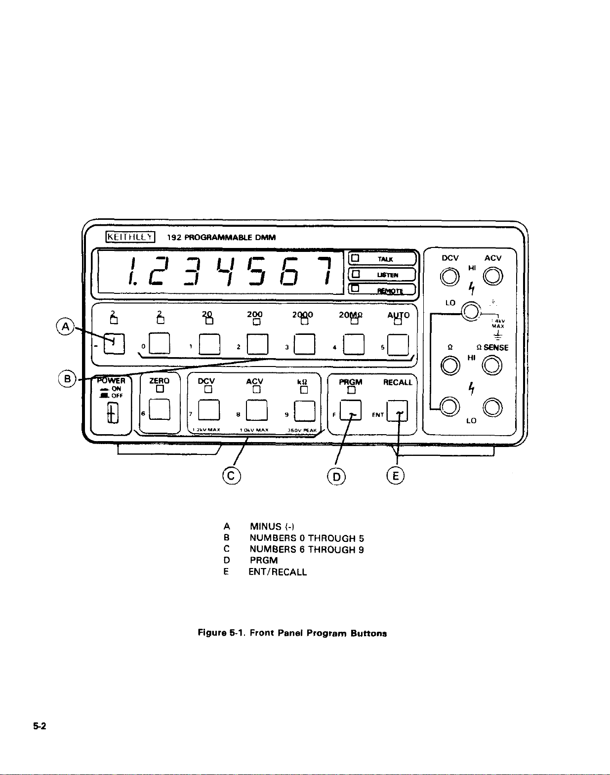
192 PROGRAMMABLE DMM
Y--c71 n n 17 17
DCV AC”
qo
6-2
A
MINUS 1-l
B
NUMBERS 0 THROUGH 5
C
NUMBERS 6 THROUGH 9
D
PRGM
E ENT/RECALL
Figure 6-l. Front Panel Program Buttons
Page 27
E. Only es many significant digits es necessary need to
be entered. The Model 192 will complete the constant with trailing zeroes where necessary.
F. Invalid keys will be ignored. If an invalid key is
depressed, the blinking “c” segment will remain at
the current digit.
G. If an incorrect digit is entered, the complete constant
must be reentered. The new value may be entered by
cycling the display around to the beginning by
repeatedly depressing one of the number buttons.
H. A neoative constant mev be entered bv deoressina
I~ I
the front panel minus (-I button. The display will the;
show a negative number. This mey be done at any
point in the numeric input sequence. Depressing the
minus button a second time will restore the constant
to s positive value.
If too many digits are entered, the display will begin
again et the first digit on the left. All the digits in the
constant must then be entered again.
Once all the digits of the desired constant are shown
on the display, the constant is entered into the program by depressing the front panel ENT button.
The number of significant digits to be entered for s
constant will depend on the display resolution mode
in use. In the 5 H digit mode, only five digits after the
leadingfi or 1 may be entered. In the 6 !4 mode, up to
six digits in addition to the leading 0 or 1 may be
entered.
10. PROGRAMS 3 through 7 will be terminated if the Model
192 receives a Remote Enable command over the
IEEE-488 bus. PROGRAM&through 2 are not affected
by the Remote Enable command.
Note
If it becomes necessary to exit a program in
progress (for example, to change resolution
with PROGRAM 1, or change the filter mode
with PROGRAM 21, readings will be missed
while the instrument waits for the operator
to enter the desired program number.
11. When the front panel PRGM button is pressed, the
instrument will prompt the operator to enter the desired
program number by displaying the following message:
Note that the question mark on the display will blink
until a program number is entered. Depressing en invalid
button at this point will result in the following message,
which will be displayed for K second:
[no]
gram, the following message will be displayed for H
second:
j-z-T-q
13. While PROGRAMS 3 through 7 era being run, the front
panel PRGM indicator light will be on. This light will go
off if the program is cancelled. either by using PROGRAM 8: or if the Remote Enable command is received
over the IEEE-488 bus.
14. The front panel PRGM button will be inoperative if the
IEEE REMOTE indicator light is on. Once the instrument
is in the Remote mode, the following IEEE command
sequence must be sent to restore front panel program-
ming operation: GTL (Go to Local); DCL (Device Clear).
For more information on IEEE commands. refer to the
Model 1923 Instruction Manual. Alternately. the instrument may be turned off and then powered-up again to
restore programming operation. Of course. any con-
stants previously stored will be lost, and the instrument
will return to the power-on default conditions.
15. When PROGRAMS 3 through 7 are entered, the AUTO
range will be cancelled. The instrument will stay on the
present range when one of these programs is entered
6.3 PROGRAM 0. CLEAR
PROGRAMtimey be used to cancel PROGRAMS 3 through
7. This program is entered by depressing the PRGM switch
followed by the 0 button es follows:
1. Press PRGM. The instrument will display the following,
indicating it is waiting for s program number:
r-Fzi-71
2. Press 0. The following message will be displayed for approximately % second:
[ml
3. Immediately following the program number indication.
the following message will be displayed for Ih second:
4. PROGRAMS 3 through 7 will be cancelled. and the
Model 192 will return to the normal operating mode by
displaying readings. The operation of the Function.
Range, and Zero buttons will be restored after PRO-
GRAM 0 is entered.
5. Depressing the RECALL button after PROGRAM fi has
been run will cuese the following message to be dis-
played for H second:
12. The Range, Function, and Zero buttons are locked out
while PROGRAMS 3 through 7 sre in progress. The operator must exit the program if these parameters are to
be changed. If en invalid key is pressed durinp a pro-
6-3
Page 28

5.4 PROGRAM 1. RESOLUTION
The display resolution of the Model 192 may be changed to
5’h or 8% digits by running PROGRAM 1. If has no effect
on the date transmitted over the IEEE-488 bus, and may be
used with PROGRAMS 3 through 7. Each time PROGRAM
1 is entered. the instrument will change display resolution
modes. Upon power-up, the instrument is in the 5H digit
display mode. To change the resolution. PROGRAM 1 may
be entered as follows:
1, Press PRGM. The Model 192 will respond with the usual
prompt for a program number as follows:
-1
normally enabled for the 6H digit mode. For a more complete description of these routines, refer to paragraph 4.6.
PROGRAM 2 controls operation of a third available filter,
filter 3. Each time PROGRAM 2 is entered, the state of filter
3 is changed. If filter 3 was previously enabled, entering
PROGRAM 2 will turn filter 3 off, If the filter was previously
disabled, PROGRAM 2 will turn the filter on. Upon power-
up, filter 3 is disabled. The mode of filter~3 may be changed
by entering PROGRAM 2 as follows:
1. Press PRGM. The instrument will respond with the usual
prompt for a program number:
r-?z-7-\
2. Press 1. The unit will indicate it has entered PROGRAM 1
by displaying the following message for H second:
3. If the instrument was previously in the 5!4 digit mode, it
will change to the 6H digit mode as indicated by the
following message, which will be displayed for approx-
imately W second:
[s.;
Readings made in the 6H digit mode are made at a
slower rata, es indicated by the flashing rate of the
decimal point.
4. If the instrument was previously in the 6H digit mode, it
will change to the 5% digit mode and display the follow-
ing message for ‘h second:
[s.s
5. After PROGRAM 1 has been run, the Model 192 will continue to display normal readings. PROGRAMS 3 through
7 may be entered et this time without effecting display
resolution.
6. Example: Assume the Model 192 is connected to a DC
voltage source and is in the 5K digit mode on the 20V
range. A tYpical 5H digit display reading might be:
r-i-Gmq
After entering PROGRAM 1, the display reading might
change to:
Note that the lest digit was roundedoff when the instrument was in the 5% digit display mode.
5.5 PROGRAM 2. FILTER
The Model 192 has a digital filter that is useful for minimiz-
ing the effects of noise on the readings. Normally, filter 1 is
enabled for the 5’h digit resolution mode, while filter 2 is
2. Press 2. The program will be entered es indicated by the
following message which will be displayed for % second:
p.YG-iq
3. If the filter was previously turned off, the filter will be
enabled, and the following message will be displayed for
H second:
4. If the filter was on, it will be disabled. end the following
message will be displayed for approximately ‘/2 second:
NOTE
If the filter is not in the desired mode, it may
be chenged by running PROGRAM 2 again.
To do this, simply depress the PRGM end 2
buttons in sequence a second time. Each
time PROGRAM 2 is entered, the filter mode
changes to the alternate state.
5. Once PROGRAM 2 has been entered, the Model 192 continues normal operation by displaying readings. Other
programs may then be entered as desired.
6. As an example of PROGRAM 2 operation, assume that
readings on the 0.2VDC range are being made. If the
displayed readings continuously or intermittently hop
around, the filter should be turned on to minimize these
effects. Note that operating the Model 192 with the filter
on will increase the response time to sudden changes in
input level: if short settling times are required, the
operator should use PROGRAM 2 to disable the filter.
See figure 4-2 for the response graph of filter 3.
5.6 PROGRAM 3. OFFSET/SCALE
PROGRAM 3 allows the operator to automatically multiply
normal display readings IX) by a constant (St and add an
offset (b). The result (YI will be displayed in accordance
with the formula, Y = SX + b. Upon power up, S = 1, and
Page 29

b=O, but these constants may be changed at the appropriate point in the program. Note that Range, Function, end
Zero buttons are inoperative during the course of the program. If one of these buttons is depressed while PROGRAM
3 is running, an “in Pro” message will be displayed. PRO-
GRAM 3 is useful when slope calculations are required for a
series of measurements. Operating instructions for PRO-
GRAM 3 are as follows:
1. Select the Function and Range, and enable the Zero, if
desired, before PROGRAM 3 is entered. These operating
controls cannot be used once the program is run.
2. Press PRGM. The Model 192 will respond with the program prompt message 8s follows:
3. Press 3. The program number will be displayed for K
second es follows:
The instrument will now prompt the operator to enter the
4
S constant by displaying the following message for ‘h
second:
[]
The old value of S will then be displayed: the most signifi-
5
cant digit will show a blinking “c” segment to indicate
that en operator entry is required. If no changes in the
displayed value are desired. the constant may be entered
by depressing the ENT button.
6.
A new value for S may be entered by depressing the
numbered buttons in the desired sequence. Note that S
must be in the range -1.999999 L S L +1.999999.
After the desired value of S is shown on the display, the
constant must be entered into the program by depressing the front panel ENT button.
7
After the S constant is entered, the Modal 192 will
prompt the operator to enter the b constant by displaying the following message for % second:
8.
The display will then show the presently stored value of
b. In addition, the first digit “c” segment will blink, indicating the instrument is waiting for an input. At this
point, the old value of b may be entered simply by
depressing the ENT button.
9
A new value for b may be entered by depressing the
numbered buttons in the desired sequence. Note that
the b must be in the range of -1999999 (b ( + 1999999
with the decimal point automatically placed according
to range. For a given range, the value of b cannot
exceed the maximum that can be measured on that particular range. For example, the maximum value of b on
the 20VDC range is f 19.99989. Once the desired constant is shown on the display, it may be entered into the
program with the ENT button.
10. Once the ENT button has been depressed, the Model
192 will show the value of Y. If the value of Y is larger
then can be handled by the particular range, an “DFLO”
message will be displayed, indicating the instrument
must be switched to a higher range. Note that PROGRAM 3 must be cancelled with PROGRAM 6 before
the range can be changed.
11. While still in PROGRAM 3, new values for S and b may
be entered by using the RECALL button. The following
message will be displeyed.for X second:
? r ,I, 3
The Model 192 will then prompt for new values of S and
b es previously described. To enter new values. follow
the procedure in steps 5 through 9 of paragraph 5.6.
12. The values for S end b will be stored within the Model
192 until the power is turned off. These constants may
be used in future runs of PROGRAM 3. Note, however,
that the value of b is scaled according to the range in
use. If, for example, s value of 19.00000 was entered for
b with the instrument on the 20V range. the value of b
will be changed to 190.0000 if the program is entered
with the instrument on the 200V range.
13. An example of readings that will be obtained when PRO.
GRAM 3 is run is shown in the following. Each of the
obtained values for Y assumes the following constants:
S = + 1.5; b= +5. Also, the instrument is on the 20
IDCV, ACV. kfll range.
Normal Reading
+8 VDC
-5 VDC
PROGRAM 3 Reading IY = SX + bl
+ 17 VDC
-2.5 VDC
6.3 VAC’ 14.45 VAC
AkR
11 kR
‘Requires AC Option
NOTE
The display resolution mode determines the
number of digits required for the b and S
constants. The range end example values
given assumes the Model 192 is being
operated in the 6X digit mode. One less
digit is required for these constants when in
the 5K digit mode.
5.7 PROGRAM 4. PERCENT DEVIATION
This program allows the user to determine how much a par-
ticular reading differs from some desired value. The percent
deviation is internally computed according to the following
formula:
Y=X-n xl00
n
Page 30

where X is the normal reading, Y is the percent deviation,
end n is the constant to which the reading is to be com-
pared. Upon power-up, n = 0 and must be changed by the
operator or the instrument will go into overflow when the
program is run. Note that the Range, Function, and Zero
buttons are inoperative when in this program; the program
must be cancelled if these parameters must be changed.
The basic procedure for using PROGRAM 4 is as follows:
1, Select the Function and Range, and Zero the instrument,
if desired, before entering the program.
2. Press PRGM. The instrument will display:
(i’
3. Press 4. The program message will be displayed for K
second as follows:
The instrument will prompt the operator to enter the con-
4
stant n for ‘h second es follows:
The present value of n will then be displayed. At this
5
point, some constant must be entered if the present value
of n = 0, or an overflow will occur. If the present value of
n is not zero, the ENT button may be used to enter the
presently displayed value of n into the program.
If a new value of n is desired, enter the number one digit
6.
at a time into the display. The value of n must lie in the
range of -1999999Ln < + 1999999. Note that the
decimal point will automatically be placed according to
range. The value of n cannot be greater then the range
currently being used. For example, the maximum value
of n on the ZOOVAC renge is 199.9999. Also, the
number of digits in the constant depends on the display
resolution. In the 5% digit mode, one less digit will
appear in the constant.
Once the desired constant is in the display, the value
7.
may be entered into the program with the ENT button.
Once n is entered, the display will show the per-
8.
cent
-199.9999yY c +199.9999. Once again, the actual
number of dig& will depend on the display resolution;
the least significant digit will be rounded off in the 5%
digit mode.
If the range of the instrument is exceeded on the per-
9.
cent deviation computation, the Model 192 will display
its “OFLO” message’.
10. A new value for n may be entered without exiting the
program by pressing the RECALL button. The instrument will respond with:
for ‘h second, followed by:
deviation
_
within the range of
r?zTTl
h I 41’
for ‘/ second. The current value of n is then displayed;
the user may then enter some other value es described
in
paragraph
11. As an example of how the Model 192 computes percent
deviation, assume that the display shows e reading of
+ 150V IX) on the 200VDC range and the value for com-
parison (n) is + 125V. The percent deviation Y will be
automatically computed by the instrument when PRO-
GRAM 4 is entered after the value of n lin this case
+ 125) is entered, es follows:
In this example, the percent deviation is positive
because the measured voltage (XI is more positive than
the comparison standard (nl. If the percent deviation
shown in the display should have e negative value, then
the measured voltage is more negative than the programmed constant.
5.8 PROGRAM 6. MINIMAX
PROGRAM 5 allows the operator to automatically store the
minimum and maximum readings that occur while the pro-
gram is being run. An example of an application for this program might be to monitor the output voltage of a new
power supply design to see how much it drifts over a given
period of time.
Operating instructions for PROGRAM 5 are as follows:
1. Select the Function and Range, and Zero the instru-
ment, if desired, before entering the program. These
paremetere cannot be changed once the program has
been entered.
2. Press PRGM to obtain the following prompt:
3. Press 5. The instrument will display the program number
for ‘h second es follows:
4. Immediately following the program number, the follow-
ing message will be displayed for ‘h second:
5. The display will continue to show the present reading.
Minimum and maximum readings are automatically
stored for recall. The stored date always contains 6%
digits even if the storage was made while the unit is in
5.7 steps 5 through 7.
X-n
Y=-x100
”
Y=FE!x,oo
125
Y=20%
F’ I- c, ‘5
5-6
Page 31

the 5% digit mode. Thus, 6% digit resolution may be
obtained for the high and low readings regardless of the
display resolution. To obtain 6’% digit resolution for
recalled readings, the instrument must be in the 6%
digit mode.
6. To display the high and low readings, depress the
RECALL button: the instrument will display the follow.
ing for K second:
I]
7. Following the program number, the following will be
displayed for % second:
[:31
This message will be followed by the low reading itself.
8. To obtain the high reading, depress the RECALL button
again. The instrument will respond with:
Elapsed
Time
0
1 hr.
2 hr.
3 hr.
4 hr.
5 hr.
6 hr.
7 hr.
8 hr.
Actual
Voltage
+ 12.006V
+ 12.01v
+ 12v
+11.99v
+ 11.987V
+11.95v
+ 12v
+ 12.OOlV
+ 12.005V
-
At the end of the prescribed time period, the operator
could check for low and high values by depressing the
RECALL button. The low value. which will be displayed
immediately after the “LO” message, is + 11.95V while
the high value for this example is + 12.01OV. To cons
tinue the test with the existing high and low values. the
operator must press the ENT button. To enter new high
and low values, the program must be started from
rhe
beginning.
[h’l
for a period of % second, after which the display will
show the highest reading obtained during the current
PROGRAM 5 run.
NOTE
The low or high reading sequences will be
cancelled if the operator attempts to run
PROGRAM 1 or 2 while reading back low
and high values.
9. To continue the program with the current high and low
values, press ENT. The instrument will begin at step 5.
paragraph 5.8.
10. To continue with new high and low values, the program
must be entered from the beginning at step 2 of
paragraph 5.8.
11. As an example of PROGRAM 5 operation, assume the
Model 192 is to be used to monitor the drift of a
+12VDC (nominal1 power supply over an eight hour
period. Once the instrument is connected to the supply,
the operator would then set the unit for 20VDC operation with the appropriate front panel buttons. The filter,
resolution, and Zero modes, may be selected as desired.
To begin the program, the user depresses the PRGM
and 5 buttons in sequence; the Model 192 then begins
storing maximum and minimum vslues. Assume the
power supply voltage actually drifted as shown in the
following:
5.9 PROGRAM 6. HI/LO/PASS
PROGRAM 6 allows the operator to set low and high
reading limits into memory. Once the limits are sat. the
Model 192 will indicate whether or not a specific reading
falls within the prescribed range. This feature is especiallv
useful for component evaluation, where certain component
tolerances must be observed. Once the limits are programmed into the instrument. the operator need only watch for
the appropriate message on the display to determine if a
particular component is within tolerance. With the optional
Model 1923 IEEE-488 interface installed. the Model 192 may
be used to control sorting and handling equipment with
suitable relays. Operating instructions for PROGRAM 6 are
as follows:
1. Select the desired Function and Range, and Zero the I”strumant. if desired. before entering the program. These
parameters cannot be changed once the program is run.
2. Press PRGM. The following message should be
displayed:
I:-]
3. Press 6. The instrument will display the program number
for % second:
4. Immediately following the program number. the instrument will prompt for the low reading limit with the
following message for X second:
57
Page 32

5.
At this point, the display will show the old value. If the
displayed value is to be used, press the ENT button.
6.
If a new value is to be entered. press the numbered but-
tons in sequence. The low value must be in the range
-lSSSSSS~LDL= ‘+ 1999999; the decimal point will
be placed according fo range. Note that the low value
cannot be numerically larger than the limits of the range
being used.
7.
Once the desired value is shown on the display, press
ENT to enter the low limit.
The instrument will now prompt for the high limit by
8.
displaying the following message for ‘h second:
The old high limif will be displayed, and may be entered
9.
by simply pressing the ENT button at this point. Note
that the high limit must be more positive than the low
limit, or the program will not run.
To enter a new high limit, use the numbered buttons in
10
the desired sequence. The value must be in the range of
-19999993 tilLi + 1999999, with the decimal point
placed according fo range. As with the LOL constant,
the high limit constant cannof have a value larger than
the limits of the range in use. Once the desired value is
in the display, press the ENT bunon to enter the
constant.
11
At this point, the instrument will run the program. No
numeric readings will be displayed. bur the instrument
will show one of the following messages, depending on
the measurment.
A. If the measured value is less than the low limit, then
“LO” will be displayed.
8. If the measured value is greater than the high limit,
then “HI” will be displayed.
C. If the measured value falls within the low and high
limits, then “PASS” will be displayed.
12
To enter new low and high values, press the RECALL
button and begin at step 4 of paragraph 5.9.
13
As an example of PROGRAM 6 operation, assume that
a batch of 10kR. 10% resistors must be checked for
tolerance. Before running the program, the operator
would place the Model 192 on the 20kR range to make
the necessary measurements. Then PROGRAM 6 is run
by depressing the PRGM and 6 buttons in sequence.
When the instrument prompts for the low value, the
operator would key in 9.000 (lOk0 -10%). When the
high limit is asked for, a value of 11.000 is entered (10kR
+ 10%). When the program is run, the instrument will
show the “PASS” message for all resistors thaf fall
within the 10% tolerance range. For those resistors with
values under SkR. the intrument will show a “LO”
message, while resistors greater than 11 k0, will cause
the “HI” message to be displayed.
14
Three open collector outputs for HI. LO, and PASS, are
available on the IEEE card. These outputs may be used
with relays to control other equipment. For further
details, consult the Model 1923 Instruction Manual.
5.10 PROGRAM 7. DATA LOGGER
PROGRAM 7 is designed to allow the operator to store up to
100 readings in an internal buffer. The reading intervals may
be sef to specific values between 0.11 seconds and one
hour. At any point in the program. readings may be recalled
from the front panel. This program is useful for such applications as the long farm monitoring of the operation of a
system. Once the data points are stored, the readings may
be recalled to determine if the system operated in the HI/LO
limits over the specified period. The operation of PRO-
GRAM 7 is ss follows:
1.
Select the Function and Range. and Zero the insfrument, if desired. These parameters cannot be changed
once the program is entered.
Press PRGM. The following message will be displayed:
2.
Press 7. The program number will be displayed for ‘/
3.
second:
4.
The instrument will now prompt the operator to input
the time interval constant r. by displaying the following
message for K second:
5.
The display will then show the current value of r. Each
digit corresponds to a given time interval as listed in
Table 5-2. Also shown is the total time required to store
100 readings. Upon power-up, r= 0, corresponding to a
time interval of 0.11 seconds for 60Hz operation.
6.
To enter the old value of r, press the ENT button.
7.
A new value r may be entered by depressing the appropriate number button. Once the desired digit is shown in
rhe display, the value will be entered into the program
by pressing the ENT bunon.
At this point, the Model 192 will not yet begin to store
8.
readings: instead, present readings will be displayed,
with the following message appearing every few
seconds.
9.
To actually begin storing readings, press the ENT button
again. The instrument will respond by logging data
points at a time interval determined by the previously
programmed value of r.
10
The readings may be retrieved at any time during the
logging process by pressing the RECALL bunon. The
Page 33

number of the reading will be indicated by the following
message:
The asterisk represents the number of the reading,
which will be displayed for !4 second, followed by the
reading itself. Note that the decimal point stops flashing
when the display shows a recalled reading.
11. After all 100 data points have been logged, the instrument will respond with the following message:
12. Pressing the RECALL button at this point, will display
the last reading in the buffer.
13. To continue recalling readings, press the RECALL button momentarily. After the number of each reading is
briefly displayed, the reading itself will be shown. If the
RECALL button is held in, the reading numbers
automatically increment in sequence.
14. To decrement the reading numbers rather than in-
crement them, press the minus l-1 button before depressing the RECALL button. The reading number will
continue to decrement with each operation of the
RECALL button until the minus button is pressed a second time.
15. Logging may be continued if previously interrupted by
pressing the 0 and ENT buttons in sequence. The
decimal point will again flash. To change the reading
time intewal or start the program over, exit the program
by using the PRGM button and begin at step 3 of
paragraph 5.10.
16. As an example of PROGRAM 7 operation, assume it is
desired to monitor the power line voltage for a computer
system over a given period of time. To do so, the
operator would switch the Model 192 to the 200VAC’
range and connect the instrument to the power line.
Once the program is entered, the operator may choose
any time interval listed in Table 5-2. For this example,
assume that a time interval of 10 minutes is desired.
When prompted to do so, the operator should key in a
value of 7 for the constant r. Once the program has run.
the Model 192 will log the power line voltage at 10
minute intervals. The instrument may be interrupted at
any time to display stored readings. Once all 100
readings are stored the “b FULL” message will be
displayed. and the operator may display the readings in
sequence with the RECALL button, as previously
described.
Table 5-2. Data Point Times
Total Time For
L
(
)t
1
2
3
4
5
6
;
9
-
tFastest reading rate of each function IDCV. KR or ACVI.
5.11 IEEE BUFFER OPERATION”
If desired, the data in the buffer may be read by commands
given over the IEEE-466 bus. However, controller must not
send the IEEE-486 REN (Remote Enable) command, or the
Model 192 will exit PROGRAM 7.
If desired, data in the buffer may be fed to an IEEE listener
such as a printer. For more complete information on accessing the buffer through the IEEE bus, refer to the Model 1923
Instruction Manual.
5.12 PROGRAM 6. SERVICE PROGRAM
As the name implies, this program is designed to aid in servicing the Model 192. It is not intended for operator use:
qualified service personnel should refer to section 6.
paragraph 6.4. for a complete description of PROGRAM 6
operation. Should the operator inadvertently enter this program, operation of the instrument may be restored by
depressing any front panel button (except POWER1 four
times in succession.
t
.ll sec.1
,126 sec.
.5 sec.
1 sec.
5 sec.
10 sec.
1 min.
5 min.
10 min.
30 min.
1 hr.
For software level E7 use Program 0 for the set-
vice program.
100 Data Points
11 sec. at 60Hz/
12.6 sec. at 50Hz
50 sec.
1 min. 40 sec.
8 min. 20 sec.
16 min. 40 sec.
1 hr. 40 min.
8 hr. 20 min.
16 hr. 40 min.
2 days 2 hr.
4 days 4 hr.
I
NOTE
I
* Requires AC option.
** Requires Model 1923 IEEE-466 option
5-s/5-10
Page 34

Page 35

SECTION 6
PERFORMANCE VERIFICATION
6.1 INTRODUCTION
Performance verification is recommended upon receipt of
the instrument, to ensure that no damage or misadjustment
has occurred during transit. Verification may also be per-
formed whenever the instrument’s accuracy is questioned
or following calibration.
NOTE
For instruments that are still under warranty
(less than 12 months since date of
shipment), whose performance falls outside
specifications at any point, contact your
Keithley representative or factory
immediately.
6.2 ENVIRONMENTAL CONDITIONS
All measurements should be made at an ambient tempera-
ture within the range of la0 to 20°C 165O to 62OF) and a
mletive humidity of less than 80%.
6.3 RECOMMENDED TEST EQUIPMENT
Recommended test equipment for performance verification
is listed in Table 6-l. Alternate test equipment may be used.
However, if the accuracy of the alternate test equipment is
not at least four times better than the instrument’s specifica-
tions, additional allowance must be made in the reading’s
obtained. Some of the equipment listed in Table 6-l is not
four times better than the Model 192 specifications because
such equipment is not readily available. In these instances.
the verification procedures indicate the equipment manu-
facturer’s specified uncertainty in determining the allowable
reading for the Model 192.
Table 6-l. Recommended Test Equipment for Performance Verification
6.4 INITIAL CONDITIONS
Before beginning the verification procedures, ensure that
the instrument meets the following conditions:
1. If the instrument has been subjected to extremes of
temperature, allow sufficient time for internal temperatures to reach normal operating conditions specified in
paragraph 6.2. Typically, it takes one hour to stabilize a
unit that is 10°C IlWF) out of the specified temperature
range.
2. Turn the Model 192 on and allow it to warmp up for IWO
hours.
WARNING
This procedure requires high voltage
and Is intended for “se by qualified teat
personnel only. Take care to prevent
contact with live circuits which could
CBUI)B electrical shock resulting in injury
or death.
6.5 PERFORMANCE VERIFICATION
6.6.1 DC Voltage Accuracy Check l2OV to 12OOV
ranges)
1. Select the DC Volts function.
2. Connect the DC calibrator (Item A. Table 61) to the
Model 192’s DCV terminal.
3. Select the 20 range.
4. Apply a positive lO.OOOOVDC to the Model 192. The
reading must be within the limits specified in Table 6-2.
5. Select the 200 range.
ITEM
A DC Calibrator
9 AC Calibrator
C
D Decade Resistor
E
DESCRIPTION
High Voltage Amplifier 1ooov
lUsed with Model 745A)
Kelvin-Varley Voltage
Divider
IUsed with Model 343Al
SPECIFICATION
1ov. 1oov. 1ooov
*o.ooz% or zopv
O.lV. 1v. 1ov. toov
* 0.022%
* 0.04%
190ll. 1.9kfl. 19kg.
190kn. 1.9MR. 1OMn
iO.Ol%
.19V. l.SV with Fluke
.Zppm Terminal
Linsariw
MFR. MODEL
Fluke 343A
H-P 745A
H-P
ESI RS725
:
746A
720A
6-1
Page 36

6. Apply a positive lOO.OOVDC to the Model 192. The
reading must be within the limits specified in Table 6-2.
7. Select the 1200 range.
WARNING
The 1200 range will overrange at vcltages war 1200V. As specified on the
front panel beneath the DCV button,
1.2kV is the maximum allowable voltage
that can be applied without damaging
the instrument.
8. Apply a positive lOOO.OOVDC to the Model 192. The
reading must be within ths specified limits in Table 6-2.
9. Repeat all checks with negative voltage.
Table 6-Z. DC Voltage Performance Check IZOV to
1200v Range
6.6.2 DC Voltage Accuracy Check L2V to 2V ranges)
1. Select the DC Volts function.
2. Select the .2 range.
3. Connect the DC calibrator (Item A, Table 6-11, KelvinVarley voltage divider (El and Modal 192 as shown in
Figure 8-l.
4. Set the DC calibrator to an output of + lO.OOOOV. Sat
the Kelvin-Varlev to .019000 lfor an output voltage of
.190000 Wltsl.
5. Dial the Kelvin-Varlay voltage divider to zsro. Than press
the Model 192 ZERO button for a display indication of
00.0000 f 1 digit.
6. Verify that the Model 192 reading is between .189975
and .190025. Note that the allowable reading includes a
i6 digit allowance for the uncertainty of the DC
calibrator and Kelvin-Varley voltage divider.
7. Repeat steps 4 through 6 with a negative voltage, and be
sure to rezero.
8. Select the 2 range. Set the Kelvin-Varley voltage divider
to .lSOOOO output. Be sure to rezero.
9. Verify that the Model 192 reading is between 1.89981
and 1.90019. Note that the allowable reading includes
*4 digits for DC calibrator uncertainty.
10. Repeat Step 9 with negative voltage. Be sure to rezsro.
Figure 6-l. Test Circuit .2mV and 2V
6.5.3 AC Voltage Accuracy Check (With Model 1910
AC Voltage Option Installed1
1. Select the AC Voltage function.
2. Connect the AC calibrator (Item 8, Table 6-l) to the
Model 192 ACV terminals. Sat the AC calibrator to 1kHz.
3. Set the Model 192 to the 2 range. Apply l.OOOOOVAC to
the Modal 192. Verify that the reading is within the limits
specified in Table 6-3.
4. Repeat steps 2 and 3 for the 20V range and then 200V
range. Apply the required voltages listed in Table 6-3 and
verify that the readings are within the limits specified.
5. To check the 1OOOV range, connect the High Voltage
Amplifier (Item C) to the output of the AC calibrator per
the manufacturer’s instructions. Select the 1OOOV range
by prassing the 2000 button of the front panel. Connect
the amplifier output to the Model 192 ACV terminals. Set
the AC calibrator for an amplifier output of lOOO.OOV at
1kHz. Verify that the Model 192 reading is within the
specified limits in Table 6-3.
6. To check accuracy at 50Hz. 2OkHz. and 100kHz. select
the 20 range, apply the voltage specified in Table 6-3 at
50Hz, then repeat at 20kHz and 1OOkHz. Verify that the
Model 192 readings am within the limits specified.
Table 6-3. AC Voltage Accurscy Check
I T Range
Applied
Voltage
Allowable Readings
at 160 to 26OC
at 1kHz
2v
2ov
2oov
1ooov
1 .ooov
1o.ooov
1oo.oov
1ooo.ov
.99868 to 1.00132V
9.9868 to 10.0132V
99.868 to 100.132V
998.00 to 1002.OOV
at 50Hz
2ov
1o.ooov
9.9868 to 10.0132V
at 20kHz
2ov
1o.ooov
9.9868 to 10.0132V
at lOOkliz
2ov
1o.ooov
9.90 to lO.lOV
For performance verification of TRMS AC volts, refer to the
Model 1920 Instruction Manual.
6.5.4 Resistance (!I) Accuracy Check
1. Select rasistancs In) function
NOTE
The .2kO and 20kR range performance
verification will be done on four-terminal
ohms, that is, utilizing the fl terminal as well
as the fl sense terminal. For four-terminal
measurements, connect the 0 sense leads to
6-2
Page 37

the circuit to be measured and the 0 sense
terminals to the Model 192. This arrangement eliminates the error clue to the voltage
drop across the current-carrying leads. The
ZERO button also accomplishes this. It is
recommended that both be used to compen-
sate for lead resistance.
2. Perform Zero function as follows:
A. Connect the Dls) terminals together (short them)
with a low thermal shorting plug.
B. Press the ZERO button and verify each We) range as
specified in Table 6-4.
Table 6.4 Zero Readings
Range
.2 kR
2 kR
20 kn
200 kR
2000 kR
20MR
3. Select the .2kR range.
4. Connect the decade resistor (Item D, Table 6-l) to the R
terminal and the R sense terminals.
5. Set the decade resistor lltem D, Table 6-l) to zero and
compensate for any residual lead resistance by pressing
the ZERO button for a display indication of .OOOOOO
* .OOOOOl flashing.
Allowable Reading
.OOOOO * 10 digits
0.0000 f 2 digits
00.000 * 2 digits
000.00 i 2 digits
0000.0 * 2 digits
00.000 * 2 digits
6.
Sat the decade resistor to O.lSOOOOkR. Verify that the
reading for the .2kR range is within the limits specified in
Table 6-5.
7.
Select the 2k0 range.
8.
Set the decade resistor to 1.90000kR. Verify that the
reading is within the limits specified in Table 6-5.
9.
Select the 20kQ range. Set the decade resistor to zero
and reset the ZERO button.
10,
Set the decade resistor to lS.OOOOkQ. Verify that rhe
reading is within the limits specified in Table 6-5.
11
Select the 200kfl range and remove R sense leads. Set
the decade resistor to zero and reset the ZERO button.
12.
Set the decade resistor to lSO.OOOkR. Verity that the
reading is within the limits specified in Table 6.5.
13. Select the 2000kn range. Set the decade resistor to zero
and reset the ZERO button.
14. Set the decade resistor to 1900.00kR. Verity that the
reading is within the limits specified in Table 6-5.
15. Select the 20MR range. Set the decade resistor to zero
and reset the ZERO button.
16. Set the decade resistor to lO.OOOOMR. Verity that the
reading is within the limits specified in Table 6-5.
Table 6-5 Resistance Accuracy Check
Range
.2 kg
2 kn
20 k0
200 kg
2000 kn
20Mfl
‘Manufacturer’s specified uncertainty of the decade resistor (DI in
digits, This uncertaino, has been added to the specified accurscv Of
the Model 192 to obtain the allowable reading.
Resistance
.190000k0 .I99960 to
1.90000kQ 1.69960 to
lS.OOOOkR 19.9960 to
190.000kR 199.960 to
lSOO.OOkR 1899.60 to
10.0000MR 9.9949 to
Allowable Readings
at 18” to 2E°C
.190040 t 19 digits
1.90040 * 19 digits
19.0040 f 19 digits
190.040 * 19 digits
1900.40 * 19 digits
10.0051 f 10 digits
*
63%.4
Page 38

Page 39

SECTION 7
THEORY OF OPERATION
7.1 INTRODUCTION
This section contains circuit descriptions for the Model 192.
Descriptions are also included for the Model 1910 AC
Option. A separate instruction manual is available for the
Model 1920 TRMS option. The information is arranged
to
provide a description of individual functional circuit blocks.
To facilitate understanding, the descriptions are keyed to
accompany simplified block diagrams and schematics.
Detailed schematics of the Model 192 and Model 1910 are
located at the end of this manual.
7.2 OVERALL FUNCTIONAL DESCRIPTION
The Model 192 isa 6X digit, ~2.000.000 counts DMM with
five DC voltage and six resistance ranges Istandard). The
unit has l@ and 1mR sensitivity with 0.00005% resolution.
When the Model 1910 AC Voltage Option is installed, AC
voltages from lo@ to 1OOOV can be measured. The most
unique feature of the Model 192 is its’ hybrid Analog-to-
Digital converter which uses both charge balance and single
slope conversion techniques. A microcomputer located
within the Model 192 controls the Analog-to-Digital conversion process. The charge balance/single slope convsrter
feature, along with the internal microcomputer, provides
many enhancements to the DMM’s performance. These
enhanced features include:
l
Extremely High Accuracy
l
High Conversion Speeds
l
Quick Settling Times
l
Reduction in the number of component parts
l
Non-Linear Digital Filtering
l
Push button nulling of any on-scale input signal
l
Automatic 2/4 Terminal Ohms Measurements
These items will be described in more detail in the latter part
of this section. Refer to Figure 7-1 for a simplified signal
flow block diagram of the Model 192.
The Model 192 is partitioned into two electrically isolated
sections, digital and analog. These sections are isolated by
opt0 isolators and by isolated secondary windings on the
power transformer. Partitioning and isolating the unit allows
the LO or common input of the DMM’s analog section to be
placed at any potential (between + 12OOV1. Simultaneously, the LO or common side of the digital circuitry can be
maintained at voltage potentials within 30V of chaws
ground. This isolation simplifies interfacing of the Model
192 with external digital equipment.
Operation of the Model 192 is centered around the AID
converter. The converter requires a conditioned analog
input for the wide range of DC inputs used, and the conversion of ohms and AC voltages to DC voltages. The A/D
Figure 7-1. Basic Block Diagram
7-l
Page 40

dc
MULTIPLEXER OUTPUT
) INPUT AMP
BOOTSTRAP AMP
100~1 DIVIDER
+2V CALIBRATION REFERENCE
I
n
TH’
f
nSENSE LO
&
3
BOOTSTRAP
VOLTAGE
em--------
r
+5V
(DIGITAL LOGIC1
I
I
L ---------- -I
ONE OF 9 DRIVERS
FOR 9 MULTIPLEXING
SWITCHING FETS I
1
I
7-2
MULTIPLEXING SWITCHING
FETS
Figure 7-2. Simplified Multiplexer Schematic (Refer to Figure 7-l. Block Al
Page 41

converter also requires various control signals and data pro-
cessing capabilities to perform the A/D ConverSion process
and to compute the results. Inputs applied to the Model 192
are switched by the multiplexer. These input signals along
with zero and full scale references are systematically switched by the Model 192. Only one signal at a time is allowed to
pass through the multiplexer which is then routed to the
Input Amplifier, this amplifier acts as a buffer and is capable
of multiplying the output of the multiplier by a gain of one or
ten.
The digital output of the AID converter inputs to the
microcomputer. Here the results of the AID conversion are
computed. and this information is sent to the display circuits
of the Model 192. If the Model 1923 remote programming
option is installed, the results of the A/D conversion are
sent to this option and will be placed on the IEEE general
purpose interface bus.
7.3 ANALOG CIRCUIT DESCRIPTION
7.3.1 Input Multiplexer
The Input Multiplexer connects one of nine signals to the
Input Amplifier. (Refer to Schematic 30976Dl. A volts or
Ohms measurement requires several inputs to be connected
to the input amplifier. Each input is connected in sequential
order. The microcomputer of the Model 192 controls the
switching sequence and determines the length of time that
sach multiplexer switch is turned on.
Switching of the various inputs and reference signals is acTomplished with nine J-FET transistors (0310. 0311, 0312,
D327, 0328, Cl334. 0339, and 0341). A problem is encountered when using J-FET transistors as switches. When
the J-FET is turned on, the low to high transistion of the
switching voltage causes charge coupling into the analog
signal the FET is switching. The effects of these transients
were eliminated by the use of software generated delays.
;lowever, it is necessary to drive the gate of each FET
switching transistor with the input signal voltage to turn it
on. That is accomplished with a bootstrap amplifier which
operates as a voltage follower. Its input is connected to all
the FET switches; therefore, its output follows the voltage
that is selected by whichever FET switch is selected bv the
microcomputer.
Gate drives for these FETs are controlled by differential
comparators IU321, lJ304. and U3051. The comparators
convert logic level signals to voltage levels suitable for turn-
ing off and on the J-FET transistor. To turn a J-FET transistor off, the comparator output transistor pulls the J-FET
gate to -2SV (see the equivalent circuit of Figure 7-2). To
turn on the same transistor, the comparator’s open collector
output transistor turns off. This allows the gate to be pulled
to the bootstrap voltage. The bootstrap voltage is virtually
the same as the drain voltage of the switching FET. For further information about the bootstrapping process, see paragraph 7.3.5. The following paragraphs discuss the operation
of the Input Multiplexer during DC volts, AC volts, and
ohms measurements.
dc
1OO:l DlVlDER
c2V CALli3RATlON REFERENCE
I
- 3ov
RANGE
IFULL SCALE)
.2V
2V
.
cl329
@12OOV INPUT A
Figure 7-3. DC Voltage Measurement
2ov
2oov
2ooov
FRONT
PANEL
I
SIGNAL
IFULL SCALE1
.zv
2v
2ov
2v
12v
7-3
Page 42

7.3.2 DC Voltage Measurement
In DC volts operation, as shown in Figure 7-3. the input
signal either goes directly to the Input Amplifier or is con-
nected across a 1OO:l attenuator with a total resistance Of
10MO. The attenuation of the DC input signal is determined
by the range selected. Three input signals to the A/D con‘verter are required for DC volts operation Le. V,,,, V,,,,
,and V
measu%j’for 16.6 msec (See A/D Converter, paragraph
‘7.3.6). Each digitized value is stored in memory and then
used to calculate a reading by the formula:
It can be seen that the zero error is subtracted from both the
signal and the reference, and then the ratio is taken.
Multiplication by two is needed because the reference is 2V.
In taking a DC reading on the bench, the voltage seen at the
high DC voltage input terminal is switched by the associated
FET to the isolating input amplifier. The amplifier then
passes the voltage to the converter. which digitizes it and
passes it on to the processor which stores it. Next, the zero
input FET is turned on and a zero input is processed and
stored in the same way. Then the output of the 2V reference
) Each signal is required to the A/D input and
1,
SIGNAL INPUT
0328 “ON”
2V REFERENCE
I
t
Figure 7-4. FET Switching Sequence for DC Voltage
Measurement (Bench Mode of Operation)
Figure 7-6. DC Voltage Measurement FET Switching
Sequence (System Mode of Operation)
circuit is processed and stored, and finally, another zero
input is similarly processed. The lest zero is necessaw
because the gain in the input amplifier is switched resulting
in a different offset voltage. When all four inputs have been
obtained, the processor calculates a reading, and displays it.
Each switching FET is allowed to stay on for a period of time
and then turned off before proceeding to the next step in
the flow chart (Figure 7-41. The “ON” time for each FET is
controlled by the Model 192’s microcomputer.
Range switching of the input signal from the 200mV, 2V or
20V range to the 200V and 1kV range is accomplished via
relay K301. The relay is controlled by a 3 to 8 decoder
(U3221. Decoding is a function of the Shift Registers of the
Al D control logic. The relay decoder is also used to select
ranges for the AC Voltage option.
In system operation, a DC voltage reading is obtained in a
slightly diierent manner to get faster results. In the OneShot mode, the meter continuously multiplexes, digitizes.
and stores zero and calibration inputs until a measurement
triggers Occurs and the input from the high terminal is
Page 43

digitized. The processor can then produce a reading much
faster then it would using the bench method.
During system operation a WAIT command can be used. A
“Wl” command programs the Model 192 to turn on 0328
for 14ms (Default condition). A “WB” command turn on
Cl328 for 4ms. The modes are only recommended for AC
voltage source resistances of less than 100kR.
7.3.3 Resistance Measurement
For resistance measurements, four inputs are required so
the Model 192 can obtain a reading by means of a
ratiometric technique. The required inputs are:
l
Ohms Reference HI
l
Ohms Reference LO
l
Ohms Sense HI
l
Ohms Sense LO
The ratiometric technique is a mathematical process that
compares numbers and then derives a ratio from them. In
the Model 192 the ratio is a voltage ratio that is created by a
common current flowing through two resistors in series.
The current passes through both a known reference resistor
and the unknown resistance. The current through both
resistors can then be determined by measuring the voltage
drop across the known resistor and then calculating the current. Once the current through the unknown value resistor
is calculated and the voltage drop across it is measured, the
unknown resistor’s value can then be calculated
Five FET switches lC1301, Q302, D303, Cl306. and Q3081
select one of five known value resistors (see Figure 7-6).
Each of the resistors is associated with a specific ohms
range. The resistor selected by the FET switches is equal to
one half of the full scale range. For example, a 10k known
value resistor is used on the 20k range. and a 1OOk resistor is
used on the 200k range.
The voltage across the selected range resistor appears at
0310 #lEF HI) and Cl333 IREF LO). The voltage across the
unknown resistor appears at Q334 (SENSE HII and Cl339
(SENSE LO). An ohms source voltage of -4OOmV is used on
the .2k ohm range, and -4V is used for all other ohms
ranges. As mentioned earlier, four input signals are required
for ohms measurements. Each signal is measured for
16.6msec. The signals are converted to a digital number
and stored in the microcomputer of the Model 192. The
microcomputer then calculates the measured value using
the formula:
It can be seen that IReEF &(RREF LoI is the voltage across
the known resistance and that IQ,,,,, “,I - (RSENsL Lo1 is the
voltage across the unknown resistor.
KNOWN
Figure 7-6. Resistance Measurement Simplified Circuit
7-5
Page 44

Switching for Ohms operation is shown in the flow chart
(Figure 7-7). In taking an ohms reading, the voltage seen at
the OSENsE.H,, !erminal is switched by 0334 to the input
amplifier, dIgItwed, and stored in memory. Next, the ohms
SENSE LO FET (0339) is turned on in the same manner.
Then the voltage at the ohms REF LO terminal is processed
and stored, and finally the ohms FIEF HI input is similarly
processed. When all four voltage inputs have been obtained, the processor retrieves the stored values. performs a
calculation for the precise reading, and displays the value.
I
II SENSE HI
Q334 “ON”
R SENSE LO
(1339 “ON”
i, REFERENCE LO
(1333 “ON”
R REFERENCE HI
Q-310 “ON”
“II
FRONT PANEL CONN.
Figure 7-8. Affect of Lead Resistance in Z-Terminal
Ohms Measurements
For 4-terminal measurements, the R SENSE leads are connected to R, and the effect of lead resistance can be
calculated as shown in Figure 7-9. It can be readily seen why
the stated accuracy for the 200kR range requires that the
effect of lead resistance be cancelled with the ZERO push
button for both Z-terminal and 4-terminal measurements.
FRONT
PANEL
CON.
“RI
RI HI
“Cl
AiD INPUTS
“1) REF HI
A/D INPUTS
V,,REF HI
Figure 7-7. FET Switching Sequence for Ohms
MeeSUrement
Up to this point, the effect of lead resistance on the
resistance measurement has not been considered. As
shown in Figure 7-8, lead resistance can affect the display
ohms reading in both Z-terminal or 4-terminal measurements. For this explanation, resistance of the test leads
have been designated as Rl-174. If SENSE HI and LO terminals are not connected to R,. the sensing occurs at the HI
and LO input terminals through resistors R, and the
displayed reading includes the resistance of Rl and R4 added to the unknown (R,I.
7-6
“RX MEASURED= “x ACTUAL
+2
x “RI x 4
R,+Rs
‘b4SE x x ‘4
with R, = 10, snd ~~ z 1OOkR
Figure 7-9. Affect of Lead Resistance in 4-Terminal
Ohms Measurements
Page 45

7.3.4 AC Voltage Measurement
7.3.5 Input Buffer Amplifier
In AC Volts operation, the Model 1910 AC Voltage Option is
installed between the AC input terminal and the Input
Amplifier (see Figure 7-10). The Model 1910 converts the
AC input voltage to a DC voltage between zero and -2”. On
other than the 2V range, the input signal is divided by 10,
100, or 1000 depending on the range selected. For AC
voltage measurements, four input signals to the AID converter are required. Each signal is measured for 16Bmsec
and ita digitized value is stored in memory.The microcom-
puter then calculates a reading using the formula:
“,, = 2lV,,HI -V,,AUTO ZERO1
~“REF-“mlo)
Where V,,HI is the Model 1910 ouput, V,,AUTO ZERO is
its DC offset, V
ground. The 2 YErequired because of the 2v reference.
Since AC volts is a four phase measurement, the maximum
conversion rate for AC volts is two readings/second.
Switching for AC volts operation is shown in the following
flow chart (Figure 7-111. In taking so AC reading, the
voltage seen at AC HI is switched by Cl311 to the input
amplifier. The voltage is then processed and stored in the
same manner as described for DC Volts and Ohms operation. Next, the AC auto zero FET 10312l is turned on and
the voltage seen there is processed and stored. The processor then retrieves the stored voltages, calculates a reading,
and displays it.
is the 2V reference, and V eO is signal
The Input Buffer (Figure 7-12) is a non-inverting low noise,
high input impedance amplifier which looks at each input
with either Xl or X10 gain. Its output is capable of voltage
swings of *ZOVDC. These parameters era beyond the cap-
abilities of a single op amp. Two op amps, one having high
input impedance/low noise characteristics IU301 I and the
other having a wide output voltage swing (U303). were
combined to produce the desired characteristics. A third
operational amplifier, U302, operates at unity gain. Its sup-
plies are bootstrapped to the input to *6V via zener diodes
VR301 and VR302 and emitter followers 0314 and D315.
This bootstrapping technique centers the 2 V8 supplies
around the input potential of U301. U301 can then handle
input signals up to f 20” while providing linear operating
characteristics.
If the input amplifier had to provide only unity gain. this
arrangement would be adequate; however, on the 0.2” and
2V ranges a gain of ten’s required. Operational amplifier
U303 supplies the outer capability for the 120” output
swing.
7.3.6 AID Converter
A simplified schematic of the A/D converter is given in
Figure 7-13 and its waveform is shown in Figure 7-14. In
operation, the output of the input buffer is applied to the
Transconductance Amplifier. This amplifier provides two
functions. It converts the input voltage to a current, which
Figure 7-10. Block Diagram AC Volts Operation
7-7
Page 46

ACAUTOZERO
and D, is enabled by C+ going low again. fq goes high and
removes the clear from U314A.j Up to this point, Its was
turned on for one clock cycle lZ*ec) and then turned off.
The earliest it can be turned on again is one clock cycle
later. Each time Its is turned on, a counter is incremented by
an inverted V-F PULSE from 4. The flip-flops divide the
clock frequency by two, limiting the maximum number Of
charge balance integrations and output counts to one half
of the clock frequency (240kHzl. In the precise 18,6msec
charge balance period, the maximum number of times that
E2 can go
16.6msec x 240kHz = 4000 counts.
Table 7-1. Settling Delays, SN on to Turn On of
high
Integrator
and be
counted is
2V REFERENCE
Figure 7-11. AC Volts Operation Flow Chart
goes to the integrator when requested, and also provides an
offset current so that its bipolar input voltages are converted
to unipolar output currents.
The A/D converter operates first in a charge balance (CBI
phase, and then in a single slope ISS) phase. A 18.6msec interval at 60Hz and 20msec interval at 50Hz were selected to
sample each input as the best compromise to achieve good
line rejection and relatively fast conversion speed.
A C8 phase is begun when INPUT DISABLE goes low. This
occurs at the completion of a delay period that allows the
signal to settle after turning on the appropriate input MUX
switch. The delay is software generated and is dependent
on the function selected, as given in Table 7-l. When
INPUT DISABLE is removed, IIN is connected to the integrator, and V, ramps positive. The D flip-flop then acts as a
comparator, providing timing and control. After V, exceeds
the D threshold of U314, Q, goes high at the next positive
going clock edge. At the next clock edge (negative going),
I& goes high and connects Its to the integrator. IcB is
greater than Zl,, maximum, and thus, V, immediately ramps
negative.
q is also low at this time which resets and holds 0, low. At
the next negative clock edge (1 cycle later). Ice is turned off
JFET
Switch
s2
53
s4
At the end of the charge balance phase, the output of the
integrator is resting at some positive voltage. The single
slope comparator output is also positive and will not switch
until the integrator output crosses zero. The comparator
output is ANDed with a one millisecond pulse in the digital
section to produce SINGLE SLOPE ENABLE. This allows
Iss to flow into the integrator. A 3.84MHz clock is counted
from the time SINGLE SLOPE ENABLE went high until the
single slope comparator changes state W, crosses zero).
When this occurs, Iss is shut off and the counting is StOP-
pad. The amount of charge quantized by lss is equal to
111024 of the charge quantized by Its. The microcomputer
multiplies the C9 counts by 1024 and adds the SS counts to
it to obtain the composite count (4.1 million maximum).
7.4 DIGITAL AND DISPLAY CIRCUIT DESCRIPTIONS
7.4.1 Microcomputer (Refer to Schematic 309750)
The microcomputer and its associated logic circuitry provide
timing and control of the Angalog-to-Digital conversion pro-
cess. Additional functions provided by the microcomputer
include operation of the Front Panel Display, implementation of Front Panel Programs, and the control of data
through the Model 1923 IEEE-188 option.
The microcomputer includes a 6808 microprocessing unit
(MPUI, a 6522 versatile interface adapter (VIA), two 2732
read only memories IROMsl, two 2114 access memories
(RAMS), an address decoder, a data bus driver (front panel
interfecal, and the necessary reset logic. (See Figure 7-15.)
The total memory utilized in this system consists of: 8K x 8
bytes of ROM ltwo 4K x 8 PROMs/U129 and U130) for program control,
qAM’slU123 and U124) for temporary storage: 8K x 8 bytes
Delays
DC”
1
1
X
lKx8 bytes of RAM (two lKx4
IlllSfll
AC\
I
1 1
1 100
1 1
7-a
Page 47

Figure 7.12. Simplified Input Buffer Schematic (Refer to Figure 7-l. Block B)
Figure 7.13. Simplified A/D Converter Schematic (Refer to Figure 7-1. Block
Cl
7-9
Page 48

/
- 1e.smsec
DELAY’
i
‘For readout Of UP prB-scB1B counter.
Figure 7-14. AID Converter Integrator Output Waveform
for the IEEE-488 option, end 16 bytes for the VIA lU132) to
control peripherals. Provisions have been made for future
memory expansion by including an additional socket on the
mother board to accomodate an additional 4K x 8 bytes of
ROM (PROMIU134).
7.4.2 Memory
Note that the total memory used I8K of ROM, 1K or RAM,
8K of IEEE-488, and 16K of VIA) is a small portion of the
entire addressing capabilities of the 6808 MPU IlJ131 I. The
microprocessor is capable of handling 64Kx8 bytes
(precisely, 65,538/E bit words). Memory locations for the
64K addresses are assigned the values 0000,, through
FFFF,,. The ROMs. RAMS, VIA, and Data Bus Drivers
(u1281 are each allotted 8K bytes of memory. An 8K byte is
reserved for the IEEE-488 option. For example: although
t
SINGLE SLOPE PHASE
- -
-
0.5msec
INTEGRATOR INPUT DISABLED -
only 1K of RAM is utilized, an 8K portion or “chunk” of
memory is reserved or dedicated for the RAM function. In a
similar manner, 8K bytes are reserved for each PROM even
though each PROM can store only 4K. 8 bit words. An additional 8K bytes are dedicated to the VIA while only 16 bytes
are used. Another 8K memory is reserved for front panel
control (Data Bus Driver, U128l however, these memory
locations are never addressed. This will beexplained in the
following paragraphs. Finally, an 8K x 8 byte in memory is
reserved for the IEEE-488 option (the option only requires
4K of memory). Refer to Table 7-2 for specific address loca-
tions reserved for the various functions. Note that an 8K
byte Of memory is not assigned (680&7FFFl.
DELAY
NEXT
- MEASUREMENT
PHASE
c-
7-10
Table 7-2. Memorv Byte Locations
Device
Selected
RAM IU123, U1241
VIA W132)
Buffer (U128)
IEEE-488
PROM W1291
Socket (U134)
PROM W1301
* Dedicated/not necessarily all utilized.
** Not assigned.
I** For future PROM expansion.
l
*** Never accessed.
MPU Memory
Byte Locations
0000-l FFF
2000.3FFF
4000-5FFF
6000-7FFF
EOOO-9FFF
AOOO-BFFF
COOO-DFFF
EOOO-FFFF
a
hItput
Oil
01
Y2
yo
04
05
Yl
r
v,
Page 49

7.43 Address Decoder
Interfacing of the microprocessor with the RAMS, ROMS,
Front Panel, VIA or the IEEE-488 option is controlled by the
Address Decoder IU1211. Partial address decoding is used in
this system. The 3 to 8 Address Decoder selects one of the
seven devices CV, isnot used) listed in the Table 7-2 vis “pper three most slgmfacant lines; A13. A14, and A15. (The
Al2 address line of the MPU is not used.1 The seven addresses determine which of the two PROMS are selected:
the upper 8K @0& through FFFF,,/U130) or another 8K
byte in memory IA000,, through 8FFF,,/U129).
Remember, the ROMs memory capacities are only half (4Kl
of the addresses allocated for them. Also selected are the
two 1 K x 4 RAMS (connected together to provide 1 K x 81.
the front panel input, the VIA, the IEEE-488 option bus, and
third PROM, are provided for expansion.
As mentioned in the preceding paragraph, the function
selected is determined by the state of the addresses A13,
A14, and A15.These address lines determine which output
is selected at the decoder (U121l in accordance with Table
7-2.0nly one of the devices will have accesa to the DATA
BUS at any time. The address decoder selects one of the
devices only after a valid memory address has been asserted
at the decoders input IE3). The valid memory address (VMA
signal) is generated by the MPU approximstely 200nsec
after 02 time. (02 is the MPU’s 1MHz output clock.) This is
sufficient time to allow for the address lines to settle. The
accuracy of this main timing signal (02) is controlled by a
4MHz external crystal, YlOl; the microprocessor then
divides this signal by four.
7.4.4 Reset
U125, U126 and U122 form a “reset” network which
together resets the MPU, VIA, and the IEEE-488 option in
the event the front panel display is not updated after a
specific period of time has elapsed due to a lost program or
power line transient.
The 1MHz timing signal from the MPU (*I?), clocks a 214
(16.3841 stage counter (U1251 whose output conditions a
second counter (U126) to enter a count down mode after a
period of 16.6msec. (lMHz-16,384=60Hz= 16.6msecl.
After the 16.6msec A/D integration period has elapsed and
display update data is not present at the output of the VIA
lPB5) because of a possible system malfunction, U126 will
continue to count down until Q3 goes low and resets the
system. As long as update data is present at PB5, the VIA
clocks this data into the Display. This same clock pulse
(CA2) inhibits the reset condition. The lead edge of CA2 is
detected at the lead-edge-detector lone-shot/U122A,
U122b, and Cl261 and presets or “loads” a 15 count into
U126. It can be seen then, that as long as data is present, a
reset will never be generated because the data pulse will
continually reload the counter back to 1111 (151 before it has
a chance to count down to 0111 171. Note that 8 CO”nt down
pulses would have to occur for a “reset” which is equivalent
t0 eight 133msec AID integration periods with no data pre-
sent. If update display data is not present within this
16.6msec period, 03 of U126 will go low and reset the MPU.
VIA and IEEE-48-w lif present). The system will re-
main reset until RESET returns high.
7.4.6 Front Panel Switch Port
Information from the Front Panel function and mode select
tion switches is placed on the Data 8”s (lines D$ through
D4 and D7) through the Data 8”s Driver IU128). The four
inputs to this tri-state buffer (switch port) are routed from
the front panel switches. Note that there are only four
switch inputs (SW&SW4). The switches are connected in a
matrix configuration such that each switch input serves
more that one function or range. Although the address
decoder has resewed an 8k byte in memory for this device
the memory loCations are not accessed or addressed by the
Bus driver. A f&h input to the Data Bus Driver is from the
line frequency 50/60Hz detector (0102).
7.4.6 Line Frequency Detector
Q102 and associated components form the 5016OHz detec-
tor. The base of Cl102 monitors the power linelfreqency “IS
R120 which is connected to the secondan, of a power s”p~
ply transformer. The 50 or 60 Hertz signal is squared off and
placed on the data bus. The MPU then determines whether
the line frequency is 50 or 60 Hertz to establish the basic i’l-
tegration period (16.6msec at 60Hzl20ms at 50Hzl. The “no
will perform as though the line frequency is operating at
50Hz if the line source is actually 400Hz. This is necessary
since 400Hz is sn even multiple of 50Hz; therefore. 8 line
pulses are required to establish the basic integration period
at a line frequency of 400Hz (the A/D cannot operate at this
speed).
7.4.7 Isolation
There is 1500 Volts isolation between the microcomputer
and the AID control logic. Isolation is achieved with fhe “se
of opto isolators AT101 through AT104. AID output data is
isolated from microcomputer by opto isolator AT104.
ATlOl, AT102, and AT103 provide isolation between the
microcomputer outputs P87, C81, CB2, and the A/D con-
trol logic.
7.5 A/D CONTROL
The conversion from analog data to digital data begins with
the integration cycle. An integration cycle begins with the
appropriate signals to the analog circuiti enabled by one or
more of the Sl through 527 lines going high. These are the
output lines of shift registers, U103/H3 and U104/E5, and
the binary-to-decimal decoder, U105/H4. The three devices
serve as output latches. Latch functions are listed in Table
7-3.
7.11
Page 50

7-12
Page 51

F
z:
ifi
E?
z:
SlO
Sll
s12
s13
s14
s15
S16
s17
S18
s19
s20
s21
s22
S23
S24
525
S26
s27
Table 7-3. Functions of Latch Outputs
Function
Pin A input of 4 to 10 Decoder
Pin B input of 4 to 10 Decoder
Pin C input of 4 to 10 Decoder
200k Ohms range select
2k Ohms range select
2V REFERENCE multiplex control
Input buffer 1OOOV range control
DC HI multiplex control
AC HI multiplex control
AC AUTO ZERO multiplex control
ZERO multiplex control
OHMS SENSE LO multiplex control
OHMS SENSE HI multiplex control
OHMS REFERENCE HI multiplex control
OHMS REFERENCE LO multiplex control
Input buffer Xl control
Transconductance amplifier range control
Input buffer X10 control
0.2k OHMS range selectl0HM.s so”rce range select
Transconductance amplifier range control
The microprocessor waits for the inputs to settle before
clocking the shift registers. The charge balance phase is initiated when the first stage ICllj of the shift register (UllOl
goes high ICB START signal). (See Figure 7.16.) When CB
START is “true” the “D” input of the charge balance flipflop, UlOB, and the input of gate U107B are et the logic “1”
state. This logic high is gated through and clears the 4 bit
divide-by-16 counter (UlOlBl. The next rising edge of the
2.4kHz clock signal sets the flip-flop whose 0 output goes
low and enables the integrator by forcing INPUT DISABLE
low. The microprocessor waits 16.66msec (the integration
period for 60Hz; 20msec or 50Hzi and the charge balance
line returns to.0. At the next rising edge of the 2.4kHz clock,
the0 output of the flip-flop goes high again and disables the
input to the integrator, ending the exact 16.66msec integra-
tion period. Notice that the clock frequencies are crystal
controlled; however, the entire process is actually under
microprocessor control at all times.
While the integration period is taking place, pulses (V-F
PULSES) are inputted into the4 bit counter IUlOlBl. When
the cwnter overflows after 16 ccwnts occur, clock pulses
are generated at its 2Q output which the VIA counts in an
internal counter lPBGl.?hese clock pulses become the most
significant bits of the result. At the end of a charge balance
phase, 4 bits of data are left on the counter. This data is
obtained by setting the remainder line to”1” 03 of the shift
register, UllO) and allowing STROBE pulses from the VIA
IPB7) to pass through gates UlOZl3. U107C to ultimately
clock the 4 bit counter. By strobing the counter in this way
and waiting for the counter to overflow, the remainder may
be determined. The number left in the counter is equal to 16
minus the number of strobe pulses. This data now becomes
the next significant 4 bits of the 24 bit result.
Figure 7-16. Charge Balance Timing
The single slope phase begins when the SS START line (Q2
output of the shift register, UllOl goes high. (Refer to
Figure 7.17.) The SS START signal controls the D input of
the single slope flip-flop, UlOBB IG21. On the next rising
edge of the 3.64MHz clock, the single slope flip-flop is set
7-13
Page 52

and its Q output is ANDed with the COMPARATOR OUT-
PUT at U107D to generate the SINGLE SLOPE ENABLE
signal. In addition, gate U102A is enabled and the 3.84MHz
clock pulses are counted et UlOlB in the same manner the
V-F pulses were counted in the charge balance phase. The
single slope phase ends when the comparator goes to a “‘fl”
and gates off the 3.84MHz clock to the counter. The re-
mainder left on the counter is again read es in the charge
balance phase. The result is added to the charge balance
phase and single slope phase. The result is broken down as
follows:
24 BIT RESULT
6 Bits-These 6 most significant bits are accumulated in the
VIA each time the 4 bit counter overflows during the
charge balance phase.
4 Bits-This is the remainder left on the 4 bit counter during
the CB phase.
6 Bits-The B most significant bits are accumulated in the
VIA each time the 4 bit counter overflows during a
single slope phase.
4 Bits-This is a remainder left in the 4 bit counter during
the single slope phase.
buffered TTL compatible 3.64MHz clock to UlOlA which
runs the charge balance circuitry within the AID at a
460kHz rate. The 2.4kHz clock is obtained by further
dividing the 3.84MHz clock with UlOlA and U106 (see
Figure 7-191. This clock is used to provide en exact
16.68msec (60Hzl or 20msec (50Hzl window and also pro-
vides the interruptions for the microprocessor.
7.6 Display Circuit
The display information is outputted on PA43 through PA6
on the VIA (1101 bus. The information is updated at a
1.2kHz rate which means each digit is ON for 633
microseconds. Each update begins by presenting nevv segment information on the VIA (l/O) bus (PA@PAGl and outputting a clock pulse on CA2. The clock pulse inputs to
U203 Snd shifts a digit enable bit to the next digit to be
enabled. Every eight times the display is updated, a digit
enable bit is generated at PB5 and goes to the enable data
input of the shift register. Refer to Figure 7.20.
The first four digit drivers drive the rows of the switch
matrix. The switches are arranged in a 4 by 4 matrix, thirteen of which are used. The columns of the switch matrix
go to Bits N-3 of the front panel switch port described in
paragraph 7.4.5. The segment drivers are 0201-0208. In
addition to driving the various segments, they also activate
the appropriate LED’s,
Figure 7-17. Single Slope Phase
One of the many functions of the VIA is to transfer data
from the digital side to the analog side of the optical
isolators. With the strobe line (PB7) HI, a data transfer
starts. One byte of data is stored in the serial register ISR) of
the VIA and is automatically clocked through the optical
isolators using the clock (CBl) end data (CB2) lines of the
serial port. Another 6 bits are clocked out of the VIA. The
strobe line (PB71 is brought LO then HI again to shift the 24
bits of data which are shifted into the latches (U103, UllO,
U1041. Four of the bits are used to address the binary to
decimal decoder (U1051. Refer to Figure 7-16.
7.5.1 Clock Circuit
The 3.84MHz clock is a Pierce oscillator using QlOl as the
gain element and a 3.64MHz crystal YlOl es the feedback
element. LlOl and Cl08 act as a parallel load. RllO, Rlll,
and Cl10 provide appropriate level-shifting compatible with
the TTL input of U107A. The output of U107A provides a
7.7 POWER SUPPLY
The power supply for the Model 192 contains the line
voltage fuse (FlOl), switching components, and a discrete
current driver. Because of the simplicity of the design, a
block diagram is not required (refer to page 2 of Schematic
30975Dl.
The components mentioned in the preceeding paragraph
generate the six voltages required for proper operation of
the Model 192. St01 is the front panel main power switch.
When this switch is in the “ON” position, AC line voltage is
applied to the primary of TlOl. 5102 (internally located)
conditions the Model 192 for 1lOVAC or 220VAC operation
by placing the two primaries in parallel or series,
respectively.
Closer observation of the schematic will note that within the
four bridge rectifiers, there are actually six rectifier circuits.
CR103 and CR104 are full-wave bridge rectifiers utilizing
their own secondaw transformer windings. CR101 and
CR102 are dual full wave rectifiers sharing a common
center-tapped transformer (e.g. The two diodes at the right
in CR101 perform the full-wave rectifier for the +30VDC
while the two at the left rectify the AC input for the
-3OVDCI. Notice the similarity in all stages. The components used in the six circuits are listed in Table 7-4 for
convenience. All circuits have filters at the outputs of the
rectifiers. The raw DC voltages are regulated and then
7-14
Page 53

bypassed. The + 15V Wllll, the -15V. the +3OV, and the
-30V are developed solely for the Analog circuits. In addition, the Analog circuits have their own + 5V supply (U127J.
The + 5V supply for the Digital Logic has a series pass transistorlhigh current gain network (0103 and Q1041 at the
Table 7-l. Power Supply Component Identification
output of its regulator W133l. CR106 compensates for the
base to emitter voltage drop across (1103. CR105 provides
short circuit limiting. Note that this is the stage where the
signal tapped off for the 50/60Hz Detector of the Digital
Logic.
Cirrent
Amp.
a1031
a104
Figure 7.16. Simplified Schematic of Latch (Refer toFigure 7-1, Block El
Figure 7.19. Simplified Oscillator/Divider Diagam IRefer to Figure 7-l. Block FI
7.15
Page 54

FROM U-126
0 s209 1 0 s2101 0 s2111 0
6
s212 1
AUTO ,20m
5 4
FROM U-132
u201
DRIVER
,I
200 200
-4
R203 l-
i
I
T
-
2000 2000
3 2
I
SWFT REGISTER
I
LE
I.-
i-1
I
PAO-PA7 A
41
B
C
D
‘Bl
II!
Figure 7-20. Display Schematic (Refer to Figure 7-1, Block Gl
Page 55

SECTION 8
MAINTENANCE
6.1 INTRODUCTION
This section contains information necessary to maintain the
Model 192 DMM and the Model 1910 AC voltage option.
Adjustment/calibration, troubleshooting, and fuse replacement procedures are provided. Calibration should be
performed yearly (every 12 months), or whenever performances verification (see Section 61 indicates that the Model
192 is out of specification. If any step in the calibration procedure cannot be performed properly. refer to troubleshooting information in this section or contact your Keithley
representative or the factory. Complete calibration and
maintenance information for the Model 1920 and the Model
1923 is provided in the instruction manual supplied with the
option.
8.2 CALIBRATION
The following paragraphs explain the calibration procedure
for the Model 192.
WARNING
This procedure requires the use of high
voltage end is Intended for qualified test
personnel only. Take care to prevent
contact with live circuits which could
ceuse electrical shock resulting in injury
or death.
8.2.1 RECOMMENDED TEST EQUIPMENT
Recommended test equipment for calibration is listed in
Table 6-l. Alternate test equipment may be used, However,
the accuracy of the alternate test equipment must be equal
to the specifications in Table 8-1,
8.2.2 ENVIRONMENTAL CONDITIONS
Calibration should be performed under laboratory condotions having an ambient temperature of 23’X + l°C. and a
relative humidity of less than 70%. If the instrument has
been subjected to temperatures outside of this range, or to
higher humidity, allow one hour minimum for the instrument to stabilize st the specified environmental conditions
before beginning the calibration procedure.
6.2.3 Warm Up
Connect the line cord to an appropriate power source lsee
paragraph 6.3.21 and depress OFF/ON push button to ON.
Allow two hours for warm up before beginning the calibration adjustments.
8.2.4 Calibration Adjustments
WARNING
Some procedures require the use of
high voltage. Take cere to prevent contact with live circuits which could cause
electrical shock resulting in injury or
death. Use an insulated tool when
making adjustments.
To make calibration adjustments:
1. Apply the appropriate input.
2. Lift off the top cover MOMENTARILY to make the
adjustment.
3. When the adjustment is made reinstall the top cover.
ITEM
A
s
C
D
E
Table El. Recommended Test Equipment for Calibration
DESCRIPTION
DC Calibrator
AC Calibrator
High Voltage Amplifier
(Used with Model 745Al
Decade Resistor
Kelvin-Varley Voltage Divider
(Used with Model 343A)
SPECIFICATION
19v. 19ov. 1ooov
@20oom
iv, ibv, ioov
220ppm
1OOOV. 400ppm
190fl. l.SkQ, 190k0
1.9Mg. 1OMR
Certified to 50ppm
O.lSV, l.SV
with 2ppm
Terminal Linearity
MFR.
Fluke
H-P
H-P
ESI
Fluke
MODEL
343A
745A
746A
RS725
720A
6-l
Page 56

A. Refer to Table 8-2 and perform the listed adjustments
in the sequence indicated. See Figure 8-l for adjust-
ment locations. Perform steps 1 through 11 to
calibrate the basic Model 192. If the Model 1910 AC
voltage Option is installed, also perform steps 12
through 19. If the Model 1920 AC voltage option is installed refer to the Modal 1920 Instruction Manual for
calibration instructions.
6. To insure that all functions and ranges ara operating
properly following calibration, utilize the performance
verification procedure in Section 6.
C. If calibration cannot be accomplished or the perfor-
mance verification procedure indicates a problem,
proceed to troubleshooting paragraph 8.3.
8.3 TROUBLESHOOTING SET-UP PROCEDURES
The troubleshooting instructions contained in this section
are intended for qualified personnel having a basic understanding of analog and digital circuitry used in a precision
electronic test instrument. Instructions have been written to
Table 8-2. Calibration Procedures
itep Function Range Applied Input
1 I R 1 20M 110MKl
n ZOOOk 1900kR
n 200k 190kR
n 20k 19kR
R 2k l.SkR
n .2k .lSkR
DV
DCV 2v 1.900000v
.
DCV 2v 0.00000”’
2
** Coarse Adjustment
*** Connect the DC Calibrator to the Model 192 so that it supplies negative voltage to the Model 132. Set the DC Calibrator
Steps 4 through 6 are to be made with 4.terminals ohm measurement. The instrument must re rezeroed using the 4.terminal
low thermal short to establish baseline before gain adjust.
Steps 12 through 19 require the Model 1910 ACV option to be installed in the Model 192. There is no need 10 proceed further
than Step 11 if the Model 1910 is not installed.
DCV 2v - 1.90000v
DCV 2ov 19.ooooov
DCV 2oov 19o.oooov
DCV 2ooov 1ooo.ooov
ACV 200V 1OOV at 5OkHz
ACV 2000V 1OOOV at lkliz
ACV 2V 1V at 1kHz
ACV 20V 1OV at lkliz
ACV 200V 1OOV at 1kHz
ACV 200V 1OOV at 50kHz
ACV 2V 1V at 50kHz
ACV 20V 1OV at 5OkHz
* Steps 8A and 86 must be performed for Rev. D and above Analog Boards IPC-560)
for 0.00000 Volts.
2V Dial Kelvin-Varley Divider
to o.oooooov Depress
Zero
Press Zero 0.00000 * 1 digit
assist in isolating the defective circuit or subcircuit. Isolation
of the specific defective component has been left to the
technician.
NOTE
If the instrument’s performance does not
meet specifications within 12 months of purchase date, contact your Keithley representative or the factory before attempting any
troubleshooting or repair other than fuse
replacement.
8.3.1 Line Power Fuse (FlOl) Replacement
If power fails, first verify that the main fuse (FlOll is not
defective before disassembling the Model 192. (If the Line
Voltage Setting is changed (S102) the fuse must be re-
placed.) The fuse is accessible from the Model 192 rear
panel. To replace. proceed as follows:
Test Equipment
Decade Resistor
1900.00 -t .5 digits
190.000 k .5 digits
19.0000 f .5 digits
1.90000 * .5 digits
.190000 + .5 digits
.OOOOO * 2 digits
1.90000 * .5 digits
R381 - 1 .soooo
R307
R353
R308
C412
R401
R410
R411
R409
C412
c411
C408
19.0000 -t .5 digits
190.000 * .5 digits
1000.00 f 2 digits
100.000 f 50 digits”
1000.00 * 4 digits
1.00000 f 4 digits
10.0000 c 4 digits
10.0000 * 4 digits
100.000 f 9 digits
1.00000 * 9 digits
Decade Resistor
Decade Resistor
Decade Resistor
Decade Resistor
Decade Resistor
DC Calibrator (with Kelvin-
Varley Voltage Divider
DC Calibrator (with Kelvin-
Varley Voltage Divider)
DC Calibrator
DC Calibrator
DC Calibrator
DC Calibrator
DC Calibrator
745 AC Calibrator
745 AC CalibratoriAmplifie
745 AC Calibrator
745 AC Calibrator
745 AC Calibrator
745 AC Calibrator
745 AC Calibrator
745 AC Calibrator
1
I
r
I
8-2
Page 57

LIN ADJ.
200k ---..
,nnnl, -
Yd
k
y* R307
R306
-a305
A304
303
Figure 8-1. Adjustment Locations
8-3
Page 58

1. Turn power off by depressing the Model 192 POWER button, and disconnect the line cord.
2. The fuse carrier is spring loaded. Using a slotted
screwdriver, push the fuse carrier in and rotate % turn
counterclockwise. The carrier and fuse will eject from the
holder.
3. Remove the fuse from the carrier and replace par Table
8.3.
CAUTION
Do not install fuse with higher rating
then specified. Instrument damage may
occur.
4. To install the fuse and carrier into the holder, reverse the
procedure in step 2.
Table 8-3. Fuse Replacement
Line
Voltage FlOl
90-125V 1/4A, 25OV, 3AG. SLO BLO
210-250V 1/8A, 25OV. 3AG. SLO BLO
Fuse
Keithley
Part No.
FU-17
FU-20
8.3.2 Line Voltage Selection
Set up the Model 192 to operate on the available AC line
voltage 8s follows:
WARNING
Turn off power and disconnect the line
cord before removing the case cover.
1. Remove the top covar.
2. Refer to Table 8-4 and sat switch 5102 accordingly.
3. install proper fuse per paragraph 8.3.1.
NOTE
The line voltage setting of the instrument is
marked on the rear panel. The following procedure can be used either to confirm the factory setting, or to set up the instrument for
operating on another voltage range, If the
line voltage range is changed, the box next
to the selected line voltage should be appro-
priately marked as an external reminder of
the setting. Use a water soluble marking
pen.
Table 8-4. Line Voltage Selection
Input Line
Switch
Voltage Frequency SlM
105V-125V 50.400Hz 115v
21OV-250V 50-400Hz 230V
‘SOV-1lOV 50.400Hz 115v
‘195V-235v 50-400Hz 230v
‘Requires special factory installed transformer.
8.3.3 Disassembly
If it is necessary to remove or replace a component, use the
followinq disassemblv procedure.
Remove the top cover as follows:
WARNING
Turn off power and disconnect the line
cord before removing the case cover.
A. Remove the two retaining screws located at the rear of
the instrument.
B. Grasping the top cover at the rear, carefully lift it off
the instrument.
C. When installing the top cover, make sure that the
three tabs located at the front of the cover engage in
the front panel assembly.
Remove the top shield from the Analog board by firmly
lifting it off the four retaining slips. Refer to Figure S-l.
When replacing the top shield, do not pinch any wires in
the retaining clips.
If the AC option is installed, disconnect the brown and
blue wires IP1014 and P1016) at the AC input and procede as follows:
A. Unplug the option from the analog board (PC-560).
B. Detach shields from PC Board by removing the two re-
taining screws.
C. Refrain from any unnecessary touching of circuit com-
ponents; handle the board by its edges.
4. Remove the Analog board as follows:
A. Disconnect the input wires (white, green, gray. black
and red1 from the analog board fPC56OJ.
B. Remove the four screws retaining the analog board.
Lift the analog board up end place it on the side of the
Model 192.
NOTE
A fifth screw may be located at the rear of
the analog board. This screw must also be
removed to saparate the analog board from
the chassis.
5. If the Model 1923 IEEE option is installed, proceed as
follows:
A. Unplug the Model 1923 ribbon cable from the mother-
board (PC-5591.
B. Remove the two screws holding the rear panel to the
chassis.
C. Remove the two screws that hold the rear panel to
the chassis (located under the Model 19231.
D. Lift the rear panel slightly and gently tap downward
on the chassis until the rear panel is dislodged from
the chassis. The Model 1923 will still be attached to
the rear panel.
E. Carefully remove the display board (PC-5301 ribbon
cable from the display board.
F. Remove the mother board from the chassis by pulling
the mother board toward the rear fawav from the front
8-l
Page 59

panel) being careful not to damage the power ON
switch.
For reassembly, perform steps A through G in reverse
G,
order.
NOTE
Recalibration of the Model 1910 AC Voltage
Option may be necessary if any of the
following occurs:
1. Removal/replacement of the 1910.
2. Disturbing position of the 1910 in the con-
nector.
3. Removallreplacement of shields on the
1910.
Refer to paragraph 6.5.3 to check AC voltage accuracy. lf
calibration is necessary perform steps 12 through 19 in Table
6-Z.
6.3.4 Special Handling of Static Sensitive Devices
CMOS devices are designed to function at very high impe-
dence levels for low power consumption. For this reason, a
normal static charge build up on your person or clothing can
be sufficient to destroy these devices. Table 6-5 lists the
static sensitive devices in the Model 192 and the following
steps provide instruction on how to avoid damaging them
when they must be removed/replaced.
1. The integrated circuits listed in Table 6-5 should be
handled and transported only in protected containers.
Typically they will be received in static protected containers of plastic or foam. Keep the devices in their
original containers until ready for use.
2. Remove the devices from their protective containers only
at a properly grounded work bench or table, and only
after grounding yourself by using a wrist strap.
3. Handle the devices only by the body. Do not touch the
pins.
4. Any printed circuit board into which a device is to be inserted must also be grounded to the bench or table.
5. Use only anti-static type solder suckers.
Table B-5. Static Sensitive Devices
:hematic
Designation
u103. u104
U106
U123, U124
U125
U126
u129
u130
u131
U132
U322
a304, a307
0329-0332
Q335Xl336
Keithlay
Pert Number
IC-261
IC-135
LSI-15
IC-197
IC-250
PRO-113-E5
PRO-105, E5
LSI-27
LSI-26
IC-166
TG-139
TG-139
TG-139
6. Use only grounded tip soldering iron.
7. After soldering the device into the board, or properly inserting it into the mating receptacle, the device is
adequately protected and normal handling can be resumed.
8.4 TROUBLESHOOTING PROCEDURE
This section contains tables listing step-by-step checks of
the major DMM circuits described in Section 7. Theow of
Operation. The following paragraphs provide instructions
for using these tables. Read this information carefully before
troubleshooting.
The Model 192 has a unique self-test feature upon power
up. This feature enables the operator or technician to make
a better judgement in isolating the problem to the Analog or
Digital portion of the DMM. Upon power up. all segments
will be displayed momentarily es follows:
[:ssasss]
Immediately following, the operator will note on the display:
Where F60 is the line frequency (basic integration period1
F60 = 6OHz
F50 = 50Hz
C4 = Software Revision Level. (This number may differ
with different instrumentsI
When this initial indication is satisfactory. it is reasonable to
assume the display and the microcomputer PROM memoi?’
are operating properly. This test enables the technician to
isolate the problem within the Analog section of the Model
192. All ranges and functions can be tested via Program 8.
When a specific range and function is selected, the program
will step the Model 192 through a four sequence test which
is the same step sequence the Model 192 uses to make a
measurementThe maior advantage of this program is that it
allows the technician to control the stepping sequence in
order to locate the problem. It also tests the display RAM
and ROM circuitry.
To use Program 6. perform the following steps:
1. Press PRGM. The instrument will prompt for a program
number as follows:
j Pro IJ
The question mark will flesh.
2. Prea 6. The instrument will display the program number
for K second es follows:
[Pro El
3. After the program number, the instrument will perform a
display, RAM, and ROM test for a few seconds. A proper-
ly operating display will appear as follows:
~maaf388:
6-5
Page 60

All front panel LED6 will also turn on.
4. If the RAM and ROM pass their respective tests, the instrument will briefly display the following message:
If the RAM teat fails. the followina rnessaqe will be
displayed:
If the ROM test fails, the instrument will disolav the follow-
ing:
rOE
5. Regardless of the outcome of the preceding tests, the instrument till continue with Program 8 operation and
prompt for a test number with the following message:
jj
The question mark will flesh.
6. A test number, l-7. may be entered et this point by pressing the appropriate button. These tests are summarized in
Table 8-6; note that tests 1 through 4 correspond to the N
modes listed in Table 8-7 of the manual.
7. If en invalid test number is entered (-, 0, 6,9, ENTI, the instrument will respond with the following message:
r-iax--
8. Program 8 may be aborted at any time by pressing PRGM.
To return the instrument to normal operation. press 0 after
pressing the PRGM button.
Table 87 indicates which particular component (FETI is ON
for a selected function and range as the program steps
through the four perts of the test IN4 through Nl, in
descending order). The Model 192 will step to the next
sequence of the test when any front panel switch is depressed. For example: After the microcomputer has been
cleared. the ZVDC function and range have been selected,
and test PROGRAM 8 has been entered; pressing a front
panel button will hold the Model 192 in the N4 mode of the
test. Refer to Table 8-7 and note that when the instrument is
set at ZVDC and the N4 is entered, the gain of the Input Buffer (Amplifier1 is 10. In addition, Cl341 is the selected
multiplexer FET that is switched ON. Scanning along N4 in
that table, reveels that Q317 (Gain FET) end Cl322 (Transconductance FET) are also ON.
1
I
This technique greatly simplifies the task of troublashooting. Press another front panel button to step the
Model 192 to the N3 mode. Notice that the multiplexer FET
selected now is Q327.
8.4.1 Line Power
In general, start troubleshooting with Table8-8 to verify that
the power supplies are providing the correct voltages to the
electronic components.
8.4.2 A/D Converter and Display
Verify proper operation of the AID converter and display
before troubleshooting the signal conditioning circuits.
Check the A/D converter and display Tables 8-9 and 8-10
respectively.
8.4.3 AC Converter
Problems with AC voltage may involve the Model 1910 AC
Voltage Option. Check this circuit per Table 8-11.
8.4.4 DC Attentuator. Ohms Source and Resistor
Problems with DC voltage or resistance ranges may involve
these signal conditioning circuits. Check these circuits per
Tables 8-12 and 8-13.
NOTE
Dust, flux, or other contamination will
degrade performance on resistance and DC
voltage ranges.
8.4.6 Digital Circuitry
Problems may exist with the microprocessor or associated
circuitry. Check per Table 8-14.
All measurements are referenced to analog common IINPUT LO terminall. unless otherwise noted in the tables.
WARNING
Some procedures in the following tables
require the use of high voltage. Take
cam to prevent contact with live circuits
which could cause electric shock resulting in injury or death. The mother board
shield is at INPUT LO potential. An input
voltage floating high enough will create
a shock hazard between the shield and
earth ground.
8-6
Test Number
14
5
6
7
Table S-S. Teat Number Summarization
Test Function Displayed Message
Nmodes1-4 None See Table 87 of manual.
ROM Test
RAM Test Passes RAM test.
Display Test
r-mcc-
M
L_rRL_I
1-l Will also turn on LED%
Comments
Passed ROM test.
Failed ROM test.
Failed RAM test.
Page 61

N2
N3
N4
2ov
2V Nl
0.2v Nl
20Mn Nl
2Mn
200kn Nl
Nl
N2
N3
N4
N2
N3
N4
N2
N3
N4
N2
N3
N4
Nl
N2
N3
N4
N2
N3
Table 8-7. Program 8 A/D Test--ET Switching Sequence
ACV
cl311
a311
cm2
Q327
a341
Q312
0327
cl341
cl311
a312
Q327
a341
a312
Q327
T
a317
1
a319 cl322
a317
I
0317
1
~
a317 Q322. (1323
I
a319
1
a319
1
03.19 I Q323
1 I
Q317
1 I
I
I
Input Buffer
Gain
Xl
Xl
x10
x10
x10
x10
x10
x10
Xl
Xl
x10
x10
x10
x10
x10
x10
x10
x10
Xl
Xl
Xl
Xl
Xl
Xl
Xl
Xl
Xl
Xl
Xl
Xl
Xl
Xl
Xl
i:
Xl
Xl
Xl
Xl
Xl
x10
x10
x10
x10
Multiplexer
FET ON
DCV
Q328
a341 a312
Q327 Q327
a341 cl341
0328
Q341
Cl327
Q341
0328 a311
0341
0327
cl341
D328
a341
CL327
a341
Q328 cl311
a341
Q327
a341 a341
a334
a339
a333
cl310
a334
a339
a333
0310
a334
a339
a333
a310
a334
a339
a333
a310
a334
a339
cl333
a310
a334
Q339
a333
a310
,
R Range
FET ON
a322
1
1
a322
1
1
a305
1
ml. a305
1
0302. a305
1
(1323 (1306. Q3071
1
1
D323
1
1
cl303, a304
1
(1306. Cl309
1
6-7
Page 62

step
1 A102 line switch
2
3
4
5
6
7 + 5V Digital
8 Emitter of 0104
9 + 15V Analog
10 Ulll Input
11 -15v
12 u112 Input
13 + 3ov
14 u113 Input
15 -30v
:
16 u114 Input
~
l
Item/Component
FlOl line fuse
PlOll line cord
+ 5V Analog
U127 Input
On optional line voltage t
Table 8-8. Line Power Checks
Required Condition
Must be set to 115V or 230V
as appropriate.*
Continuity
Plugged into live receptacle
Turn on power
+5v, *5%
+7.4V minimum
+5v, *5%
+ 6V minimum
+15v *lo96
+ 17.9V minimum
-15v. flO%
- 17.9V minimum
+3ov, * 10%
+ 36V minimum
-3ov. flO%
- 36V minimum
Jnit
8 set to 115v.
Table 8-9. AID Converter Checks
T
Remarks
see paragraph 8.3.2
see paragraph 8.3.1
P1009 pins 9 Et 10, U127
output
Output of CR103
JlOlO, pins 1,2 (IEEE con
nector)
Unregulated Input
P1009, pin 3, Ulll outpu
CR102 output
P1009-1, u112 OUtpUt
CR102 output
P1009-2. u113 OUtpUt
output Of CR101
P1009-4, u114 OUtpUt
Output of CR101
step 1 Item/Component
2 Display
3
4
5
6
7
8
9
10
11
12
13 External voltage
14
15
16
17
U312 pin 12
R326
U308 pin 2
U316 pin 2
C308 lin)
C308 lout)
External voltage
source
Display
source
Display
External voltage
source
Display
Required Condition
Turn on power. Select
1000VDC.
000.00 +2 Digits
0 to + 4v square wave at
480kHz
20V for 16.6ms. OV for 1OOms
-2.5V. *7% (175mV)
+5V, *7% (350mV)
OV, *15mV
See waveform per Figure 7-14
Select 2VDC range
Apply + 1.9OOOOV
1.90000 * 10 digits
Select 200mVDC range
Apply .OOOOOOV
Depress ZERO
00.000 * 1 digit
Apply + 190mV
190.000 f 10 digits
I
Remarks
Some tests here could fail due
to Digital board problems and
vice versa.
480kHz clock
Input Suffer output
Transconductance Amp Bias
Charge Dispenser bias
Integrator input
Integrator OUtpUt
Calibrated point
If different, check 2V reference
Q327 kmrce)
Calibrated point
Input offset nulled
Calibration point
If different, check 0.2V
reference or X10 gain of Input
Buffer.
8-8
Page 63

Table S-10. Display Checks
Step 1 Item/Component
I1 I
2
3 U203 pin 1
4 U203 pin 8
5 U202 pins 4 and 5
S
;
2
3
4
+ 5V Digital U203
pins 2,9,14 or J1008.
pin 14
tern/Component
i&
1 I
-
lisplay
I
.
(
X311 source
.
I
X312 source
External voltage
I
source
I
Display
,
311 source
I
IX312 scwce
External voltage
1
source
I2
Display
m&r~*d voltage
I3
Table S-11. AC Converter Checks (Model 1910)
) Required Condition Remarks
Turn on power. Select 1OOOVDC
range.
+5v *5%
Negative-going pulse I+ 5V to OV)
occurring every 4OOqaac. 12.5kHz).
Required Condition
Turn on power and select
2VDC range.
Short input
.00020 * 10 digits
1omv
Same as step 4. plus reading
at step 3.
Apply l.OOOOOV rms at 1kHz
1 .OOOOO + 100 digits
- 1V. plus reading at step 4
Same as step 5
Select 20VAC range
Apply lO.OOOOV rms at 1kHz
10.0000 -t 100 digits
Select 200VAC range and apply
lOO.OOOV rms.
Initial power up test
checks all digits.
If low, check per
Table 8-6.
Update data
Clock input
Remarks
Full scale input on all
ranges should produce
approximately - ZVDC at
output. P1014 (brown
wire) on the Analog Board
Do not perform unless
AID test are completed.
Normal zero offset range.
Impedance mater to
measure I > 1oSnl. Output
resistance is 300kR.
ACV Auto zero.
Calibration point,
DC outp”t
Auto zero
If any of above checks
fail, proceed to bias
checks step 18.
Calibration point
Calibration point
I4
I5
I6
I7
18”
-
External voltage
source
Display
100.000 + 100 digits
Select 1OOOVAC range
Apply lOOO.OOV rms
1000.00 + 100 digits
TURN OFF POWER. Remove
Modal 1910 AC Voltage Option
from Model 192. Remove shields
and reinstall the 1910 in the 192.
Select 2VAC range and short
Input. Turn on power.
Calibration point
With shields removed,
display will be noisy and
read many millivolts of AC
pickup. Display will also
change with operator
mo”eme”t.
I
8-9
Page 64

Table 8-11. AC Converter Checks (Model 1910) (Cont.1
Step Item/Component
19
20 R405, CR401
21
22
23
24
l
U401 Pin 2
R402,R406
Cl404, base
Q403, emitter
(1401, base
‘On Analog Board
* Model 1910 must be recalibrated if step 18 was performed.
ItemlComponent
External voltage
Display
External voltage
source
Display
External voltage
source
Display
Required Condition
ov * 1OmV
OV *lOmV
OV *lOmV
-7.5v * 10%
+ 5.7v * 10%
-3.6V *lo%
Table 9-12. DC Attentuator Checks
Required Condition
Turn on power. Select
200VDC range.
Apply + 19O.OOOV
19OJO * 10 digits
Select 20VOC range
Apply + 19.OOOOV
19.0000 f 10 digits
Select 1OOOVDC range
Apply + lOOO.OOV
1000.00 i 5 digits
Remarks
Summing junction, AC
amplifier
DC oputput before filter
Feedback circuit
Base voltage
5 milliamp current source
Bias for C404 protection
circuit.
Remarks
r
These checks should not be
made if a problem exists on
the 200mVDC or 2VDC
ranges.
Calibration point
100~1 Attenuator
Calibration point
10: 1 Attenuator
Calibration point
1OOO:l Attenuator
i
8-10
Page 65

Table S-13. Ohms Source and Resistors Checks
Step
1
2
10
11
12
13
14
15
16
17
18
19
20
21
22
23
24
Item/Component
Display
WlO. source
0344, collector
0310, sourca
Q344. collector
1 .OOOOOkR
Display
Q310. source
INPUT HI
lO.OOOOkR
Display
lOO.OOOkQ resistor
Display
1 .OOOOM R resistor
Display
lO.OOOMO resistor
Display
Required Condition
Select 200 range and short
input with 18 guage (or lower)
copper wire (tin plated okay).
Less than 00.010
-0.4v *9%
-0.4v i7%
Select 2kR range
.OOOOO i2 digits
-4v *7%
-4v *7%
Apply to input W-wire
connection)
1.00000 * 10 digits
-4v *7%
-2V +7% (half of step 11)
Apply to Input and select
20kO range
10.0000 f 10 digits
Repeat Steps 11 and 12
Apply to Input and select
200kn range.
100.000 it 10 digits
Repeat Steps 11 and 12
Apply to Input and select
2000kR range.
1 .OOOOO f 30 digits
Repeat Step 18
Apply to Input and select
20MR range.
10.0000 * 100 digits
Repeat Step 18
Remarks
30 not perform unless AID
:onverter and DC attenuator
tests are completed.
Two wire offset, including
thermals
3hms reference voltage
3hms reference divider
3hms reference voltage
3hms reference divider
Calibrated resistance
Range resistors
Ohms reference voltage
Voltage across unknown
Calibrated resistance
Range resistors
Calibrated resistance
Range resistors
Use meter with high input
impedance ( ) 1OW
Calibrated resistance
Range resistors
Use meter with high input
impedance ( > 1OW.
Calibrated resistance
Range resistors
Item/Component
U131 pin 39
U131 pin 37
U122 pin 9
UlOl pin 5
U106 pin 13
U131 pin 40
P1008 pin 15
P1008 pin 16
Table B-14. Digital Circuitry Checks
Required Condition
Turn on power. Select 1OOOVAC I
range*
0 to c4V square wave et 4MHz
0 to +4V square weve at 1MHz
0 to +4V square wave et 1MHz
0 to +4V square wave at 480kHz
0 to +4V square wsve at 2.4kHz :
c5v *5%
Negative going pulse ( + 5V to OVI
occurring every 833eec
Negative going pulse ( + 5V to OVI
occurring every 100eec
Remarks
Some tests here could fa
I
because of AID Convert1
problems end vice verse.
4MHz clock
1MHz clock
1 MHz
480kHz clock
2.4kHz clock
Reset line
Latch enable for Display
Board IPB51
Clock input for Display
Board (CA2)
L
il
3r
8-1118-12
Page 66

Page 67

SECTION 9
REPLACEABLE PARTS
9.1 lNTROOUCTlON
This section contains replacement parts information,
schematic diagams and component location drawings for
the Model 192. Panel and Covers are shown separately in
Figure 9-1.
9.2 PARTS LIST
Parts are listed alphabetically in order of their circuit
designation. See Table 9-1.
9.3 ORDERING INFORMATION
To place an order or to obtain information concerning
replacement parts, contact your Keithley representative or
the factory. When ordering, include the following
information:
Table 9-1. Model 192 Drawing Package
DESCRIPTION
AC Converter
Mother Board
(Digital and Power
Supplies)
Analog Board
Display Soard
SCHEMATIC COMPONENT LAYOUT
29960D 29955c
30975D
1 30976D 1 308310
1 309740 308230
1. Instrument Model Number
2. Instrument Serial Number
3. Part Description
4. Circuit Designation (if applicable)
5. Keithley Part Number
9.4 FACTORY SERVICE
If the instrument is to be returned to the factory for service,
complete the service form which follows this section and
return it with the instrument.
9.5 SCHEMATIC DIAGRAMS AND COMPONENT
LOCATION DRAWINGS
Schematic diagrams and component location drawings
follow the replaceable parts list information contained in this
section. See Table 9-l.
ASSEMBLY
PC-496
30824D
PC-559
1 PC-560
PC-530
9-l
Page 68

9-2
Figure 9-1. Exploded View With Mechanical Parts
Page 69

Table 92. AC Converter PC496. Pana List
Circuit
Deslg.
c401
C402
c403
c404
c405
C408
GUI7
c409
c409
c410
c411
C412
C413
c414
C415
C418
CR401
CR402
CR403
CR404
CR405
CR408
CR407
CR408
J1008
J1007
JlOOB
0401
cl402
a403
(1404
Q405
R401
R402
R403
R404
R405
R408
R407
R409
R409
R410
R411
R412
R413
R414
R415
R418
R417
R419
u401
Description
.5&F, 5OV. Metallized Polycarbanate
1OpF. ZOV, Aluminum Electrolytic
3.3rF. ZOV, Aluminum Electrolytic
BBOpF. 3V. Tantalum’
.22uF. 50V. Matallired P&carbonate
BB2OpF, 83V. Polystyrene
41BpF. 5OOVDC. Mica
Adjustable Capacitor, .819pF
3OpF. 5OOV. Mica
l&F. SOVDC. Tubular Ceramic
.2<1 &F, 200OV. Trimmer
.25-1.5pF. ZOOOV, Trimmer
lpF, IBVDC, Ceramic Disc
1OpF. ZOV, Aluminum Electrolytic
.05#F. 1OMPJ. Ceramic Disc
1OpF. 1OOOV. Ceramic Disc
Diode. Diffused. Silicon, lN914
Diode, Diffused, Silicon, lN914
Diode, Diffused, Silicon, lN914
Diode. Diffused, Silicon, lN914
Diode, Diffud, Silicon, lN914
Diode. Diffused. Silicon. lN914
Diode. Diffused. Silicon, lN914
Diode. Diffused. Silicon, lN914
Connector. Female. 12 Contacts
Lug. Receptacle
Lug, Receptacle
Transistor, NPN, Silicon, 2N5099
Transistor. PNP. Silicon. 2N5087
Transistor. PNP: Silicon, 2N6097
Transistor, NPN, Silicon, 2N3904
Transistor, PNP. Silicon, 2N3906
Pot, son. 10%. %W
249G. .l%. l/lOW, Wire Wound
ZlSlKJ, .l%, l/lOW, Wire Wound
150kfl. 5%. XW, Carbon or Composition
150kfl. 5%. ‘/W, Carbon or Composition
1Okil. 5%. %W. Carbon or Composition
284.2tI. 5%. Part of a Matched Set
24Ofl. 5%. % W. Carbon or Composition
Pot. loon. 10%. %W
Pot, 1OkQ 10%. %W
Pot, IktI. 10%. +‘.W
4.75k. .5%. Part of a Matched Set
54.7k. .5%, Film
Thick Film, 5%. Resistor Network
495k. .5%, Part of Matched Set
33klI. 5%. %W. Composition
47kG. 5%. %W, Composition
ZMSI, .5%, Part of Matched Set
Monolothic J-FET OP AMP, LF356
LocatIon
ich. Pcb.
F3 5102
F4
8103
F3
7103
9183
S/82
2
D8
lo/B2
05
ll/C2
12/u
05
04
13lCZ
14102
s
15lD2
81
18/U
Cl
17103
c2
lBlD3
62
19/E2
F2
24183
E2
25/B3
D2
26183
F5
27183
E5
29183
E5
29/B3
82
30lD2
31/u
82
SW
34lC3
82
35/Fl
c2
3wA3
E4
45lA2
E4
48/02
F2
47183
02
4B/B3
c2
49fC2
F3
52102
E4
53/ 82
F3
54182
G2
55182
F2
58182
F4
57183
D6
59i 82
D2
59183
D5
60182
D3
81/B2
04
62/C2
c5
83/BZ
64182
c4
SW
65/C2
c3
86/C2
D4
61102
El
68/u
69/U
62
72lD2
c2
Par? Nd.
C-201-.56
c-314-10
C-321-3.3
C-297-690
c-201-22
c-29SBB2op
C-278419~
C-225
C-2353Op
c-292-1.50
C-216
C-216
C-236-. 1
c-314-10
C-298-.05
c-84.lop
RF-29
RF-29
RF-29
RF-28
RF-25
RF-29
RF-29
RF-29
CS-337.12
LU-90
LU-90
TG-62
TG-81
TG-61
TG-47
TG-84
RP-99-50
R-241-249
R-241-2191
R-76150k
R-7615Ok
R-76.10k
R-266
R-76240
RP-99-100
RP-BS-10k
RP-9Slk
R-288
R-27554.7k
TF-72
R-266
A-7633k
R-7547k
R-266
IC-152
l
Manufacturers Designation includes Pan Description: e.g.. CR 25, 22, 5%
**Manufacturers Designation is GP %. 1%. TlOO, Resistance Value.
Page 70

Table 9.3. Mother Board PC-569, Parts List
CIrdt
Deaig.
AT-101
AT-102
AT-103
AT-104
c-104
c-105
C-106
c-107
C-108
c-109
c-110
c-111
c-112
c-113
C-l 14
c-115
C-l 16
c-117
C-118
c-119
c-120
c-121
c-122
C-123
C-126
C-126
c-129
C-132
c-134
c-135
c-137
C-138
c-139
c-140
c-141
C-142
c-143
c-144
c-145
c-146
c-147
CR-101
CR-102
CR-103
CR-104
CR-105
CR-106
F-101
F-101
J-1006
J-1009
J-1010
J-1011
L-101
a-101
cl-102
a-103
Q-104
R-101
R-102
Description
Optical Isolator, 6N137
Optical Isolator, 6N137
Optical Isolator, 6N137
Optical Isolator, 6N137
.lpF, 16V, Ceramic Disc
.lpF, 16V. Ceramic Disc
.1&F, 16V. Ceramic Disc
.lpF, 16V. Ceramic Disc
66pF. 1OOOV. Ceramic Disc
47pF. 1OOOV. Ceramic Disc
.lpF. 16V. Ceramic Disc
.lpF, 16V. Ceramic Disc
.lpF, 5OV. Ceramic Disc
lOpF, 25V. Aluminum Electrolvtic
lOpF, 25V, Aluminum Electrolytic
1OrF. 35V, Aluminum Electrolytic
1OpF. 35V. Aluminum Elect&tic
479F. 35V. Aluminum Electrolytic
47O@F, 35V. Aluminum Electrolytic
47OpF. SOV. Aluminum Electrolytic
47OrF. 5OV. Aluminum Electrolytic
22OOpF. 25V. Aluminum Electrolytic
lO$F, 25V. Aluminum Electrolytic
.lpF, 5OV. Ceramic Film
6EOOpF. 5OOV. Ceramic Film
22pF. 1OOOV. Ceramic Film
22pF. 1OOOV. Ceramic Film
O.lpF, 5OV, Ceramic Film
11.6OOpF. 25V, Aluminum Electrolytic
22OOpF. 5OOV. Ceramic Disc
47OpF. 2OOOV. Ceramic Disc
47OpF. 2OOOV. Ceramic Disc
.lpF. 5OV. Ceramic Film
.l@F. 5OV. Ceramic Film
4.7~F, 2OV. Tantalum
.lpF. 5OV. Ceramic Film
.lpF, 5OV. Ceramic Film
.lpF, 5OV. Ceramic Film
.lpF, 5OV. Ceramic Film
.luF. 5OV. Ceramic Film
l~F,‘SOV,‘C&mic Film
RECTIFIER BRIDGE 11.5A). PF40
RECTIFIER BRIDGE l1.5A). PF40
RECTIFIER BRIDGE (5AI. .+EO5
RECTIFIER BRIDGE 15AI. PE05
Silicon Diode, lN914.
Silicon Diode. lN4607
FUSE, % AMP (115VI
FUSE, l/6 AMP (23OV)
CONNECTOR
CONNECTOR
CONNECTOR
Power connector
1OOpH
N-Channel, J-FET, 4392
NPN. Silicon, 2N3904
NPN, Silicon, 2N3904
High Gain Darlington, D45El
10k. 5%. ‘/rW. Composition
lOk, 5%. XW, Composition
Location
Sch. Pcb.
l/E2 83
l/W
83
l/W
l/El
l/G3
l/F2
l/F3
l/F5
l/F6
l/F6
l/E6
l/M
l/F4
2lD3
2lD3
2lD3
2lD4
2/u
2/D3
2/u
2/D4
2lC2
2/D2
l/E6
l/E5
l/B3
1183
i.2
7/83
8183
S/B3
10/a
11/w
12lC3
13/D3
14103
15/B3
16/D2
17/D2
lSlD2
lS/D3
20/El
21/u
22lE2
23/W
24/W
26/4E
26165
29lC4
31ID4
32/M
35/D4
2/C5
2104
N/A
N/A
l/B1
l/A3
1 IA6
l/B6
l/E6
l/C5
l/C6
l/E3
l/E6
2lC3
2/C3
2/u
2lC4
2lE5
2/05
2iA4
2lA4
l/H1
l/H1
2/A5
l/F6
l/F6
l/D6
2105
2104
l/G4
l/G1
37lE4
391F4
4OlE4
411F4
421C4
43/F5
44/c5
45185
46184
1711D3
172/D4
173/83
174/E5
49lF2
5O/F2
511F3
52/F4
53/E4
541 E4
62lG4
62/G4
72/2C. 21
73lF5
74lG4
63lC3
77lD3
78/E5
79lE4
801 F4
95/82
66/B2
Kalthley
Part No.
IC-292
III-292
IC-292
IC-292
C-23&.1
C-238.1
c-238.1
C-238.. 1
C-64-6&l
C-64470
C-238.;
c-238.1
C-237-.1
c-314-10
c-314-10
c-309-10
c-309-10
C-299-470
C-284470
c-292-470
C-292-470
c-290-2200
c-314-10
C-237. 1
c-zz-6socm
C-64-22p
c-6422ll
C-237..i
C-314-11600
c-22-22oop
C-324-4701,
C-324.470~
c-237-.1
C-237-.1
c-179-4.7
C-237.. 1
C-237.. 1
c-237-.1
C-237.. 1
c-237-.1
C-237-l .O
RF-46
RF-46
RF-46
RF-48
RF-29
RF-41
FU-17
FU-20
30575A
CS-369-2
cs-399.1
cs-366
CH-14
TG-77
TG-47
TG-47
TG-127
R-7610k
R-7610k
Page 71

Table S-3. Mother Board PC-669. Parts List ICont.1
:ircuit
>esig.
q-103
t-104
7-105
7-106
7.107
q-109
q-109
7-l 10
S-1 11
7-112
7-115
7-116
7-117
7-120
7-121
q-122
7-123
q-124
q-125
q-126
q-127
3.129
R-129
R-130
R-131
R-132
R-133
s-101
s-102
T-101
u-101
u-102
u-103
u-104
u-105
U-106
u-107
U-106
u-109
u-110
u-111
u-112
u-113
u-114
u-120
u-121
u-122
U-123
U-124
U-125
U-126
U-127
u-129
u-129
u-130
u-131
U-132
u-133
Y-101
Y-102
Description
10k. 5%. %W, Composition
2200. 5%. %W, Composition
22Oil. 5%. ‘/W, Composition
22OQ 5%. % W, Composition
22011. 5%. %W, Composition
220.5%, NW, Composition
IOMEG, 10%. %W, Composition
4.7k. 5%. %W, Composition
4.7k. 5%. %W, Composition
Thick Film Resistor Network
10k. 5%. %W. Composition
lk, 5%. ‘/W, Composition
1.5k. 5%. %W, Composition
10k. 5%. ‘/W. Composition
4.7k. 5%, %W. Composition
47MI, 5%. %W, Composition
4700, 6%. %W, Composition
47M2, 5%. %W. Composition
47Ofl. 5%. ‘/W, Composition
1M. 5%. %W. Composition
5.36k. 1%. 1/6W. Film
2430, 1%. lI6W. Film
2.67k. 1%. l/SW, Film
12ln. 1%. 1/6W, Film
3.3k. 5%. %W. Composition
10k. 5%. ‘/rW, Composition
Thick Film Resistor Network
Switch, Power
Switch
K-l Transformer
Duel 4 Bit Counter, 74LS393
Quad. Z-Input Nand Gate, 74LSOO
9 Bit Shift Register. MCI4994
8 Bit Shift Register, MCI4094
ECD to Decimal Decoder. CD4028
Dual 4 Bit Counter. 74LS390
Quad 2-Input And Gate. 74LSO6
Dual “0” Flip-Flop, 74LS74
Ouad 2-Input Nand Gate. 7400
6 Bit Shift Register. MCI4094
+ 15V Regulator. 76M15
-15V Regulator, 79M15
Regulator, LM317
-24V Regulator, LM337
Ouad Exclusive OR Gate, 7496
Dual 2 to 4 Line Decoder, 74LS139
Quad 2-l,, Nand Gate. 74LSOO
1024 x 4 Bit Static Ram, 2114
1024x 4 Bit Static Ram, 2114
Oscillator/Clock. MC4060
Up/Down Counter. 74C193
+5v Regulator. 7905
Bus Driver, MC14503
K-l Programmed ROM
K-l Programmed ROM
Microprocessor. MC6606
Interface Adapter, SY6522
5V Regulator. 76605
3.84 MHZ Crystal
4.0 MHZ Crystal
Location
Sch. Pcb.
l/Cl 67102
l/52
l/E3
l/E4
l/F1
l/F5
l/F6
l/E6
l/E6
SEV
l/D5.E4
2/D5
2lD4
l/E6
l/D6
l/F2
l/F3
l/F4
l/El
2/65
-
-
2lA4
2lA3
2/&C
2.3.4
l/G2
H6
Fl.G2
H2
l/H3
l/F5
l/H4
l/G6
IAZ.A3.F2.F5
1 /F3.G2
l/Fl.Gl.G2
l/G4
z/o2
2/D3
2/ D3
2/ D4
l/El.E4
l/D3
l/D5,E5,W
l/D5
l/C6
l/E4
l/E4
Z/D2
l/D6
1165
l/65
l/B2
l/C2
2lD4
l/F6
l/B3 166104
68163
69/83
SO/E3
91/u
92/C3
93/u
94103
96/D3
96164
99/E4
lOO,E4
lOllE4
104lE5
105/E5
106163
107/63
106/93
lOS,C3
llOlE4
llllE4
163/U
164/E3
165/E3
166lE4
169104
170104
112lSl
113/Gl
116,117
F2
119/62
120/62
12l/C2
122lC2
123/02
124163
125/83
126/C3
127/C3
126/D3
129,El
130/u
131152
132/E3
139/64
139.c4
14OlC4
141104
142104
143lE4
144lE4
145/F3
146194
147/c4
14wc5
149/04
1501D5
151/F4
167/C3
Wthley
brt No.
q-7BlOk
3.76-220
q-76220
q-76-220
3.76.220
q-76-22
9.7810M
R-7647k
9-764.7k
TF-99
R-78101:
R-7611;
R-7615k
A-7810k
R-764.7k
R-76-470
R-76470
R-76470
R-76470
R-761?.’
R-685.36k
R-66-243
R-BB2.67k
R-68-121
R-763.3k
R-7610k
TF-101
SW-426
SW-397
TR-160
TR-199
IC-213
X-163
K-251
IC-251
IC-135
IC-212
IC-215
IC-144
IC-36
K-251
IC-194
IC-195
IC-306
IC-309
K-116
IC-182
K-163
LSI-15
LSI-15
IC-197
IC.310
IC-93
IC-250
PRO-113.E5
PRO-lOSE5
LSi-27
LSI-26
IC-223
CR-13
:R-10
s-6
Page 72

Table 94. Analog Board PC-560, Parts List
I
Circuit
I
Dssig.
,
Z-301
,
Z-302
,
z-303
,
z-304
I
z-305
,
z-307
,
3-306
I
z-310
,
C-31 1
,
C-312
I
c-313
I
C-314
I
z-315
I
CR-301
,
CR-302
,
CR-305
,
CR-306
I
K-301
I
P-1009
I
P-1012
I
P-1014
,
a-301
I
O-302
,
n-303
/
n-304
cl-305
O-306
n-307
n-309
a-309
Q-310
Q-31 1
Q-312
o-313
Q-314
cl-315
Q-316
a-317
Q-316
a-319
Q-321
D-322
Q-323
Q-325
G-327
Q-326
G-329
Q-330
a-331
Q-332
G-333
a-334
Q-335
Q-336
Q-337
cl-336
a-339
a-340
Description
6SpF 5% 5CW Polystyrene
33OpF 5% 5OOV Polystyrene
68OOpF 20% 5OOV Ceramic Disc
6BOOpF 20% 5OOV Ceramic Disc
1OOOpF 5% 5OOV Polystyrene
15OpF 10% 1OOV Ceramic Disc
36OOpF 5% 5OOV Polystyrene
1OOOpF 5OOV Polystyrene
.lpF 16V Ceramic Disc
1OOOpF 5OOV Polystyrene
.lpF 16V Ceramic Disc
1.5pF. 5OV. Tubular Ceramic
.lpF. 5OV, Ceramic Film
Diode Current Unit, J505
Diode Current Unit, J505
Diode. lN914
Diode, lN914
Relay 2PDT
Cable Assembly
connector
Connector
N-Channel FET
N-Channel FET
N-Channel FET
N-Channel FET, PF5301
N-Channel FET, 2N4392
N-Channel FET
N-Channel FET, PF5301
N-Channel FET
N-Channel FET. PF5301
N-Channel J-FET
N-Channel J-FET
N-Channel J-FET
Selected low leakage Transistors
NPN Silicon. 2N5551
PNP Silicon, 2N4355
NPN Silicon, 2N5551
N-Channel J-FET
N-Channel J-FET
N-Channel J-FET
N-Channel FET. 2N4392
N-Channel FET, 2N4392
N-Channel FET. 2N5432
N-Channel FET. 2N4392
N-Channel J-FET
N-Channel J-FET
N-Channel J-FET PF5301
N-Channel J-FET PF5301
N-Channel J-FET PF5301
N-Channel J-FET PF5301
N-Channel J-FET
N-Channel J-FET
N-Channel J-FET PF5301
N-Channel J-FET, PF5301
N-Channel J-FET. PF5301
N-Channel J-FET. PF5301
N-Channel J-FET’
Selected Device
Location
Sch.
2/81
2lC2
2lC5
2lC5
l/D1
Pcb.
7lC2
WC2
l/c3
2lC3
ll/C4
ZIG5 13lD4
Z/F2 14lF4
l/D2 16/C4
l/W
l/A3
l/D6
2104
2/85
l/D1
2lG5
l/D1
17/F5
w/04
lSlF5
24lD3
25/ D3
2SlC4
2WD4
lSO/C4
A5.61
E4,E5
l/B2
l/D2
1164
1184
l/C4
l/C4
l/E4
l/B4
l/C4
l/D4
l/D4
l/W
l/F2
l/F2
l/D4
2164
2185
2/ 83
2102
2184
2102
21 El
2/ D2
Z/D1
2lG6
l/F2
l/D1
l/D1
2lA2
2/Al
l/G2
l/G2
l/E3
l/E3
l/D3
36/D,
37lD5
39lC4
43/83
44163
45/63
46/62
47/c3
a/c2
49/c2
5OlC2
51 /c2
52/c3
WC3
54lC3
55/c3
55/ 03
57lD3
56lD3
58, D3
60/ D3
61 /D3
63/E3
64/ F2
65lF2
67lE4
7o/c4
71lC4
72lC4
73lC4
74/c4
75/c3
76/C4
77/c4
7S/B3
79/83
l/D3 BOlE4
l/G2 El/C4
l/D3
62/C4
Ksithlsy
Pan No.
C-136.68p
c-136.33op
C-22.6800~
C-22.6600~
c-13S-looop
C-64.150~
C-136-36000
C-136-1000~
C-236-.1
c-136-10000
C-236-.1
C-282-l&F
C-237-.1
TG-140
TG-140
RF-26
RF-29
RL-51
CA-12-2
29995A
cs-357
31841A
31641A
31841A
TG-139
TG-129
31641A
TG-139
31841A
TG-139
30966A
30966A
30966A
26234A
TG-67
TG-90
TG-67
30966A
309tEA
30966A
TG-126
TG-128
TG-151
TG-128
30966A
30966A
TG-139
TG-139
TG-139
TG-139
30966A
30966A
TG-139
TG-139
TG-139
TG-139
30966A
26234A
Page 73

(
Circuit
I
Deslg.
,
a-341
,
a-342
(
n-343
,
n-344
I
n-345
,
D-346
,
3-347
,
s-346
,
3-349
,
a-350
I
R-301
I
R-302
I
R-303
I
R-304
I
R-306
I
R-306
I
R-307
I
R-308
I
R-309
I
R-310
I
R-311
R-312
I
R-313
I
R-314
I
R-315
I
R-316
I
R-317
I
R-318
I
R-319
R-320
I
R-321
I
R-322
I
R-323
I
R-324
R-326
I
R-328
R-330
R-332
/
R-333
I
R-334
R-335
R-336
R-338
R-339
R-340
R-341
R-342
u-343
R-344
R-345
R-346
R-347
R-346
R-349
R-350
R-351
R-352
R-353
R-354
R-356
Table S-4. Analog Board PC-680. Parts List IC0nt.l
DeSCIlptlOIl
N-Channel J-FET
NPN, MPS-US5
NPN Silicon, 2N5551
NPN HI Volt Silicon, TIP.49
Selected Device
NPN Silicon, 2N3904
PNP Silicon, 2N3908
PNP Silicon, 2N3906
PNP Silicon 2N6067
PNP Silicon, 2N5067
50k Cermet Pot
54 Cermet Pot
6000 Cermet Pot
5OC Cermet Pot
200k Cermet Pot
20k Cermet Pot
1000 Cermet Pot
1000 Cermet Pot
l.lOBM .l% %W Metal Film
140k 1% 1/8W Metal Film
1.005k .l% l/lOW Metal Film
100.7k .l% 1IlOW Metal Film
9.9& .l% l/low Metal Film
100.6 .l% l/low Metal Film
13.3k 1% 1/8W Metal Film
lk 1% YIW Composition
Matched 8et with R319
1OOk 1% %W Composition
Matched 881 with R317
1M. 5% %W Composition
1M. 5% %W Composition
Thick Film Resistor Network
1OOk 1% %W Composition
1OOk 1% %W Composition
50k .l% l/low Metal Film
Thick Film Resistor Network
1M 6% %W Composition
2OOk 1% Y.W Composition
1On 1% ‘/W Composition
1On 1% %W Composition
1M 6% %W Composition
1M 6% %W Composition
1M 6% %W Composition
300k 5% ‘hW Carbon
300k 5% %W Composition
Thick Film Resistor Network
1M 5% YIW Composition
1M 5% %W Composition
9.99M .l% Metal Film
300k 5% XW Composition
300k 5% XW Composition
1M 5% %W Composition
300k 5% ‘/W Composition
300k 5% %W Composition
200k 1% l/8, Metal Film
1OOk 5% %W Composition
Thick Film Resistor Network
2000 Cermet Pot
lhl 5% %W Composition
1M 5% %W Composition
l.OCOtlOn
Sch. Pcb.
l/F2
l/D1
l/F3
Z/G5
z/F5
21 F2
2/w
ZIG2
2lD4
21D5
llA4
1104
1104
1184
l/C4
l/W
z/c2
z/c2
l/B3
l/C3
l/W
1183
l/B3
l/D3
l/D3
Z/El
z/C3
Z/El
z/c2
2/ 63
2/ t34
WC4
84104
65/D4
86/ D5
07lE4
88lF4
ES/F4
9O/E5
91/F5
92/F5
lOS/BZ
106/82
107/u
1owC2
lOS/CZ
llO/C2
llllC2
llZ/CZ
113/82
114/82
1wc2
11wC2
117/C2
1wc2
119/u
120/u
lZl/CZ
122/a
123lC2
124IDZ
125/D2
Dl-3.E2.3
21 D3
Z/D2
Z/D1
Z/El.F1-4
2/ 82
Z/83
2184
2185
l/G3
l/F3
l/F3
l/C5
l/W
lA4-6.l3.M
l/G3
l/G3
l/A4
l/D4
l/D3
l/G3
l/C3
l/D2
l/Al
l/B2
l/A2.1-2
127/F2
126/F2
13O/FZ
132lF3
134/D3
136/D3
137/D3
138103
139/c3
140/a
142/C3
143/c4
144/C?
145/K
146/83
147183
148183
149184
150/84
151/84
152184
153/c4
154/c4
155/a
15wc5
l/B2 157185
l/F3 15wc4
l/F3 16O/C4
26/U
Part Nd.
30966A
TG-133
TG-67
TG-137
20234A
TG-47
TG84
TG-84
TG-61
TG-61
RP-8950k
RP-ES-5k
RP-89500
RP-69.50
RP-89.20Ok
RP-8920k
RP-89.100
RP-89100
R-2641.108M
R-86-140k
R-263.1.005k
Ii-263.100.7k
R-263-9.9&
R-263-100.5
R-86-13.3k
R-76-11;
R-292.LIk
R-76100k
R-292-72.&
A-7BlM
R-76-1M
TF-111
R-76100k
R-7610Ok
R-263.50k
TF-85
R-761M
R-76200k
R-7610
R-7610
R-761M
R-751M
R-761M
R-282.300k
R-282-300k
TF-108
R-76lM
R-761M
R-2949.99M
R-282.300k
R-282.300k
R-761M
R-282.300k
R-262.300k
R-247.200k
R-282.100k
TF-83
RP-69-200
R-761&l
R-761M
97
Page 74

Table S-4. Analog Board PC-660, Parta Lilt lCont.1
Circuit
Deslg.
R-357
R-359
R-360
R-361
R-362
R-363
R-364
R-367
R-366
R-369
R-370
R-371
R-372
R-376
R-377
R-379
R-379
R-360
R-361
R-382
u-301
U-302
u-303
u-304
U-306
U-306
u-307
U-308
u-309
u-310
u-311
U-312
u-313
u-314
u-315
U-316
u-317
U-316
u-319
U-320
U-321
u-322
UR-301
UR-302
UR-303
v-301
V-302
v-303
v-304
v-305
Description
1M 5% %W Composition
Thick Film Resistor Network
209k 1% YI W Composition
Thick Film Resistor Network
220k 10% HW Composition
lOOk, 10%. 1W. Composition
1M 5% YW Composition
S&XXEd
S&Cted
Thick Film Resistor Network
2OG cemlm PO1
Resistor sat 45.Sk
Resistor set 20k
2.67k 1% l/SW Metal Film
80.4k 1% l/SW Metal Film
40.2k 1% l/SW Metal Film
1OOk 2W 10% Composition
699 .l% l/low, Metal Film
1oOk Pot
3.3M 5% %W Composition
OP.AMP Selected
OP.AMP, LF356
OP-AMP, LM343
Clued Comparator, LM339
Cluad Comparator, LM339
atlad Comparmor, LM339
J-FET Input OP-AMP, LF351
J-FET Input OP-AMP, LF351
Comparator, LM311
Transistor Package, CA3086
Transistor Package, CA3066
Guad Z-In. NOR Gate, 74L502
J-FET Input OP-AMP, LF351
Dual “D” Flip-Flop, 74574
J-FET Input OP-AMP, LF351
J-FET Input OP-AMP. LF351
Voltage Reference
Guad Comparator. LM339
Cud Comparator, LM339
J-FET Input OP.AMP, LF351
Cluad Comparator, LM339
BCD to Seven Seg Driver, 4511
6.3V Zener
6.3V zenet
S.lV 2ener
Jumper
Jumper
Jumper
Jumper
Jumper
Locmlon
Sch. Pcb.
l/G3 161 IC4
SEV
l/F3
-
2164
ZIG4
ZIG6
l/C5
l/C5
l/C6
l/C5
l/C6
ZIG6
z/F6
z/F6
l/81
l/AZ
2/R
2/Q
Z/Al
2lA6
Z/81
l/R
SEV
z3
2/Q
z/F3
I,Fl,F3
Et
z/F2
32. HZ
l/C5
2lD4
l/D6
Z/G6
l/Cl
Z/S4
2166
l/D1
z/C4
2lC5
l/C5
l/D5
l/D5
163/D4
164/D4
165/D4
1661E4
167lE4
16SIE4
171/E5
172IE5
173/E
174/E5
175lE5
176/E5
lSDlE4
181/W
162/W
163lC‘l
184105
lSSIF4
1961F3
192/C3
193ID3
194/C2
195/02
lSB/DZ
197/Q
196/Q
lSS/F3
ZOO/F3
20110
202/u
203lE4
2D4lF4
205/F4
206F4
207/F5
2OSlF5
20SlD3
2101D‘l
2111D4
212/D4
213/B
222164
223104
224lD4
229/D?
230lD3
2311D4
232/D4
233lD4
Kelthlsy
Part No.
R-761&?
TF-109
R-76200k
TF-105
R-l-220k
R-2-100k
R-76-1M
Selected
Selected
rF-110
RP-SS-20
R:29345,9k
R-293-20k
R882.67k
R-8860.4k
R-Slb40.2k
R-5100k
R-263-699
RP-97-100k
R-763.3M
30167A
IC-162
IC-254
IC-219
IC-219
IC-219
30154A
30154A
IC-173
2919SA
2SlSSA
IC-179
K-176
K-216
30154A
30154A
29996
IC-219
IC-215
30154A
IC-219
IC-166
DZ-56
DZ-56
DZ-14
J-3
J-3
J-3
J-3
J-3
S-9
Page 75

Table 9.5. Display Board PC-530. Parts List
Circuit
De&.
c-210
DS-201
DS-202
DS-203
DS-204
DS-205
DS-206
DS-207
DS-206
DS-207
DS-210
DS-211
DS-212
DS-213
DS-214
DS-215
DS-216
DS-217
DS-219
DS-219
DS-220
DS-221
DS-222
a-201
a-202
a-203
a-204
o-205
a-205
a-207
a-209
R-201
R-202
S-201
s-202
S-203
S-204
S-205
s-205
S-207
s-205
s-209
s-210
s-21 1
s-212
S-213
u-201
u-202
U-203
Dascriptlon
lO#F, 2OV. Alum Elect
” f ” Digital Display
“5” Digital Display
“5” Digital Display
“6” Digital Display
“5” Digital Display
“5” Digital Display
“5” Digital Display
Pilot Light
Pilot Light
Pilot Light
Pilot Light
Pilot Light
Pilot Light
Pilot Light
Pllot Light
Pilot Light
Pilot Light
Pilot Light
Pilot Light
Pilot Light
Pilot Light
Pilot Light
PNP SIL Transistor. 2N4355
PNP SIL Transistor, 2N4355
PNP SIL Transistor, 2N4355
PNP SIL Transistor, 2N4355
PNP SIL Transistor. 2N4355
PNP SIL Transistor, 2N4355
PNP SIL Transistor, 2N4355
PNP SIL Transistor, 2N4355
Thick Film Resistor Network
Thick Film Resistor Network
Switch
Switch
Switch
Switch
Switch
Switch
Swkch
Switch
Switch
Switch
Switch
Switch
Switch
MDS to LED Segment Driver. 75492
MOS lo LED Segment Driver. 75492
Bit Shift Register, 74LS164
LocatIon
Sch. Pcb.
D5
62 a/02
E
D2
D2
Q
Q
Q
Q
Q
H3
H3
G3
z
G3
F3
F3
F3
G3
E
G4
G4
H4
H4
G4
F4
F4
G4
F4,G4,H4
F5.G5,H5
84
A4
A4
54
64
A4
A4
64
A3
A3
83
63
84
33, 4, C3. D3
14, D4. E4, F4
c5
3/D3
9182
10102
lllC2
lZlC2
13/C?
14lC2
lS/DZ
15/02
17lD2
16163
19/83
20183
21/C3
22/w
23/D3
24/D3
25153
26183
27/W
20lC3
291 D3
33/D2
34/D2
35lD2
35lD2
37/D2
39102
39/c3
4OlDZ
46/c2
47102
51/B3
52/63
53/83
54/u
55/u
56/ D3
57lD3
58163
59183
6O/C3
61/U
621D3
63lD3
67163
66/c3
6% U
Kslthley
Psn No.
c-175-10
DD-31
DD-30
DO-30
DD-30
DD-30
DD-30
DD-30
PL-57
PL-67
PL-67
PL-67
PL-67
PL-57
PL-57
PL-67
PL-57
PL.67
PL-67
PL-57
PL-67
PL-67
PL.57
TG-60
TG-90
TG-50
TG-90
TG-90
TG-60
TG-90
TG-90
TF-165-l
TF-77
SW-435
SW435
SW-435
SW-435
SW-435
SW-435
SW-435
SW435
SW-435
SW-435
SW-435
SW-435
SW435
IC-169
K-159
IC-127
5-s/5-10
Page 76

0
e
I
9-1119-12
Page 77

I
0
0
0
I
v
Y
t
u
r
n
i
I
L
”
1:
5
!O
-
Page 78

Figure 43. Mother Board. Component Location Draw-
ing. Dwg. No. 36624 isheet 2 of 21
%15/B-16
Page 79

.- I N
I m
I n I
Page 80

Figure 94. Analog Board. Component Location Draw-
ing. Dwg. No. 30831 lshwt 2 of 21
Page 81

Figure 9-5. Display Board. Component Location Draw-
ing. Dwg. No. 30823
9-2119-22
Page 82

Figure 9-b. AC Convsrcer. Shematic Diagram. Dwg.
No. 29960
92319-24
Page 83

1
-
2
-
1
4
-
-
t
4
Figure 9.7. Mother Board. Schematic Diagram. Dwg.
No. 30975 (sheet
1 of 21
925/ 9-26
Page 84

TIOI
‘5”
Figure 9-7. Mother Board. Schematic Diagram. Dwg.
No. 30975 (sheet 2 of 21
9-271920
Page 85

w I
---- -_---.
ANGE RESlSTORS
Figure 9-8. Analog Board. Schematic Diagram. Dwg.
No. 30976 lshwt 1 of 21
9-2919-30
Page 86

Figure 9%. Analog Board. Schematic Diagram. Dwg.
No. 30976 laheet 2 of 2)
9-n I932
Page 87

a bL60E _
1
2
3
t
4
5
6
Figure 9-9. Display Board, Schematic Diagram, Dwg.
No. 30974
9-33/s-u
Page 88

SERVICE FORM
Model No.
Name
Company
Address
City
List all control settings and describe problem.
Show a block diagram of your measurement system including all instruments connected (whether power
is turned on or not). Also describe signal source.
Serial No.
state
P.O. No. Data
Phone
ZiP
(Attach additional sheets as necessary.)
Where is the measurement being performed? (factory, controlled laboratory, out-of-doors, etc.)
What power line voltage is used?
Frequency?
Variation?
Any additional information. (If special modifications have been made by the user, please describe below.)
*Be sure to include your name and phone number on this service form.
OF. Rel. Humidity?
Ambient Temperature?
Variation?
OF.
Other?
Page 89

Page 90

 Loading...