

Page 1
Instruction Manual
Model 191
Digital Multimeter
01979, Keithley Instruments, Inc.
Cleveland, Ohio, U.S.A.
Page 2
TABLE OF CONTENTS
6-1
6-l
6-1
h-l
6-l
6-l
6-2
6.2
ii
Page 3
MODEL 191 DMM
GENERAL INFORMATION
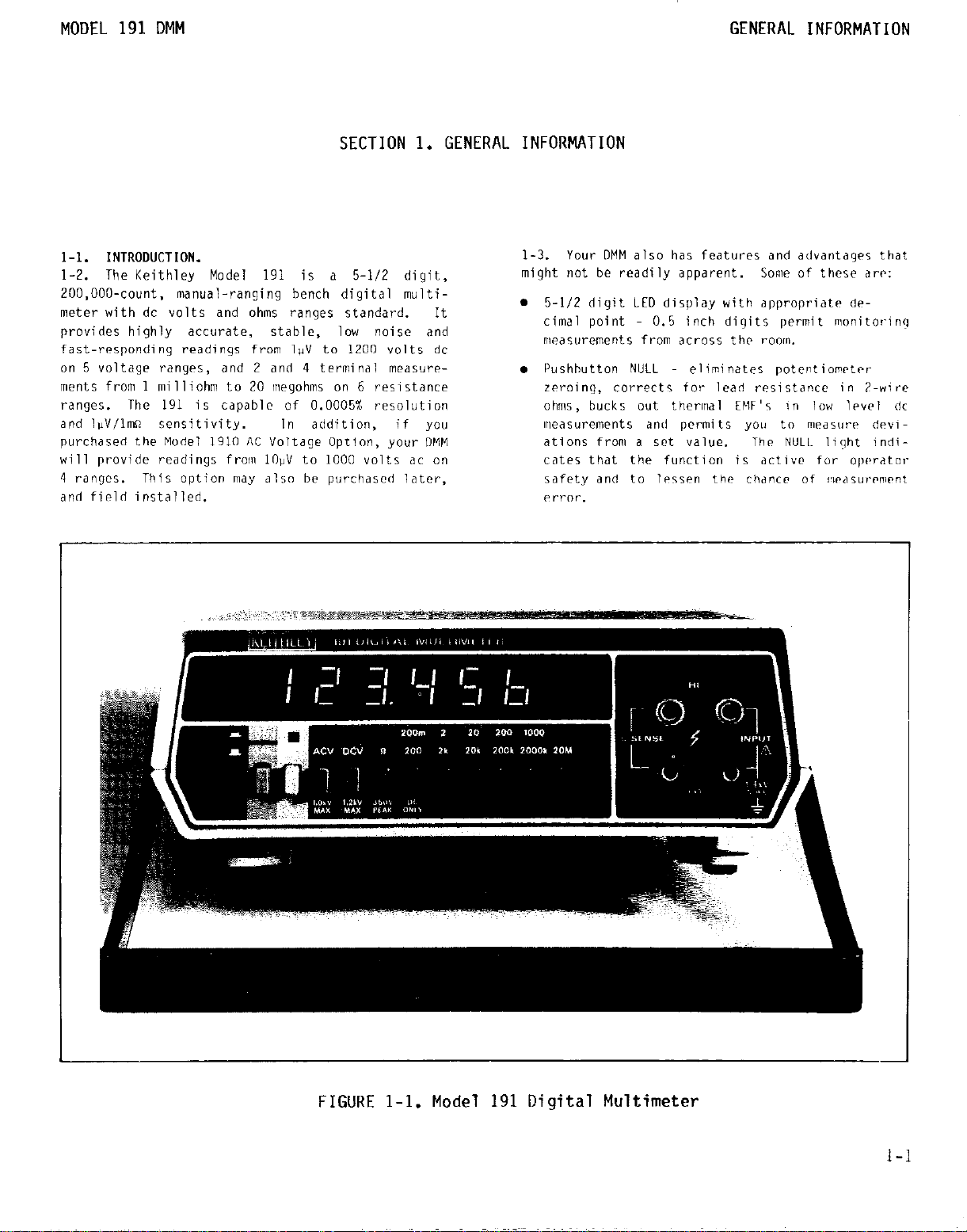
SECTION 1. GENERAL INFORMATION
l-l.
INTRODUCTION.
1-2.
The Keithley Model 191 is a 5-l/2 digit,
200,000-count,
meter with dc volts and ohms ranges standard. It
provides highly accurate, stable, low noise and
fast-responding readings from 1uV to 1200 volts dc
on 5 voltage ranges,
ments from 1 milliohm to 20 lrlegohms on 6 resistance
ranges. The 191 is capable of 0.0005% resolution
and luVlln!G sensitivity. In addition, if you
purchased the Model
will provide readings from 1OuV to
4 ra"gES. This option may alsn be purchased later.
and field installed.
manual-ranging bench digital multi-
and 2 and 4 terminal measut-e-
1910 AC
Voltage Option, your "MM
lOO(1 volts ac on
1-3. Your OMM also has features and advantages that
might not be readily apparent. Soae of these aw:
. 5-l/2 digit LEO display with appropriate de-
cimal point - 0.5 inch digits permit monitorinq
nx?asurements fron1 across tllc r""!".
l
Pushbutton NULL eliminates potenti"mrtPr
zeroing, corrects for lead resistance in ?-wire
ohms, bucks out thermal EMF's in 1ow IPYPI dc
nleasurements 3°C permits you t" medsuv? deviations from a set value. The NULi~ light indicates that the function is dctivc for "p~rat"rsaietv and to lessen the? ChdrlCC Of I.IP‘3S,II'P,~IPnt
FIGURE
l-l.
Model
191
Digital Multimeter
I-1
Page 4
GENERAL INFORMATIOP
MODEL
191
DMM
Continued.
l-3.
A Micro-processor
provides:
A Combination of single slope and charge balance
AD conversion - for faster response and better
linearity.
Automatic non-linear digital filtering - for
faster response
display.
A reduction in the number of parts while maintaining high accuracy and speed of measurement simplifies high accuracy measurements and calibration of the instrument and provides higher
mean time between failures.
-1EEEEE error message indicates improper
uses of the instrument - prevents erroneous readings and reduces possibility of injury to the
user or damage to the instrument.
Each range has:
Automatic polarity operation minus sign displayed, positive implied.
Effective input overload protection.
Overrange indication - polarity and overrange
digit displayed.
Decimal point positioned by range pushbutton.
Automatic Z/4 wire ohms operation - saves
time and simplifies Z-wire or 4-wire ohms
measurements.
A full line of optional accessories that
exterd the measurement capability of your llcdel
191.
IGOO High voltage Probe allows your Dill1 to
measure fron 12OOV to 40kV dc.
1901 Plug-l" Current Adapter allows your D,,,, to
read dc current from lvA/digit to 2000mA.
the AC Voltage option, it reads from lOti/digit
to 2000nA ac.
1682 High Frequerxy (RF) Probe allows your Dills to
RedSUre fr0n 0.25v to 3ov t-lx ac wer a frequency
t-awe of 100kHr to 1OOMHr.
without the AC Voltage Option.
1685 Clamp-On AC Current Probe (when used with AC
Voltage Option) allws your Dllll to measure fron
zero to 200A rns ac.
Some of these accessory ncde1s are:
based design that
and reduced noise on
It can be used
the
Hi th
1651
50.Ampere Current shunt allows your D!IM to
measure fron O-50A dc, ard with AC Voltaqe Option
fron IOA to 50A ms ac.
NOTE
Refer to Section 4 for more detailed information
on these accessories.
l-4. WARRANTY INFORMATION.
1-5. The Warranty is given on the inside front cover
of this Instruction Manual. If there is a need to
exercise
Representative in your area to determine the proper
action to be taken. Keithley maintains service
facilities in the United Kingdom and West Germany,
as well as in the United States. Check the inside
front cover of this Manual for addresses.
l-6.
l-7.
which occur after printing of the Instruction Man-
ual will be explained on a Change Notice sheet
attached to the inside back cover.
1-8.
1-9. Safety symbols used in this manual are as
follows:
The b
this Manual.
CAUTION statements with regard to proper use and
handling of the instrument.
instrument may occur if these precautions are
ignored.
This\ ~
this Manual.
on the instrument which are potential shock
hazards.
statements with regard to proper use and handling
of the instrument.
result if these precautions are ignored.
l-10.
I-11.
given in Table 1-I.
the warranty, contact the Keithley
CHANGE NOTICES.
Improvements or changes to the instrument
SAFETY SYMBOLS.
IMPORTANT
symbol can be found in various places in
Carefully read the associated
Oamage to the
svmbol can be found in various places in
This symbol indicates those areas
Carefully read the associated WARNING
Serious personal injury may
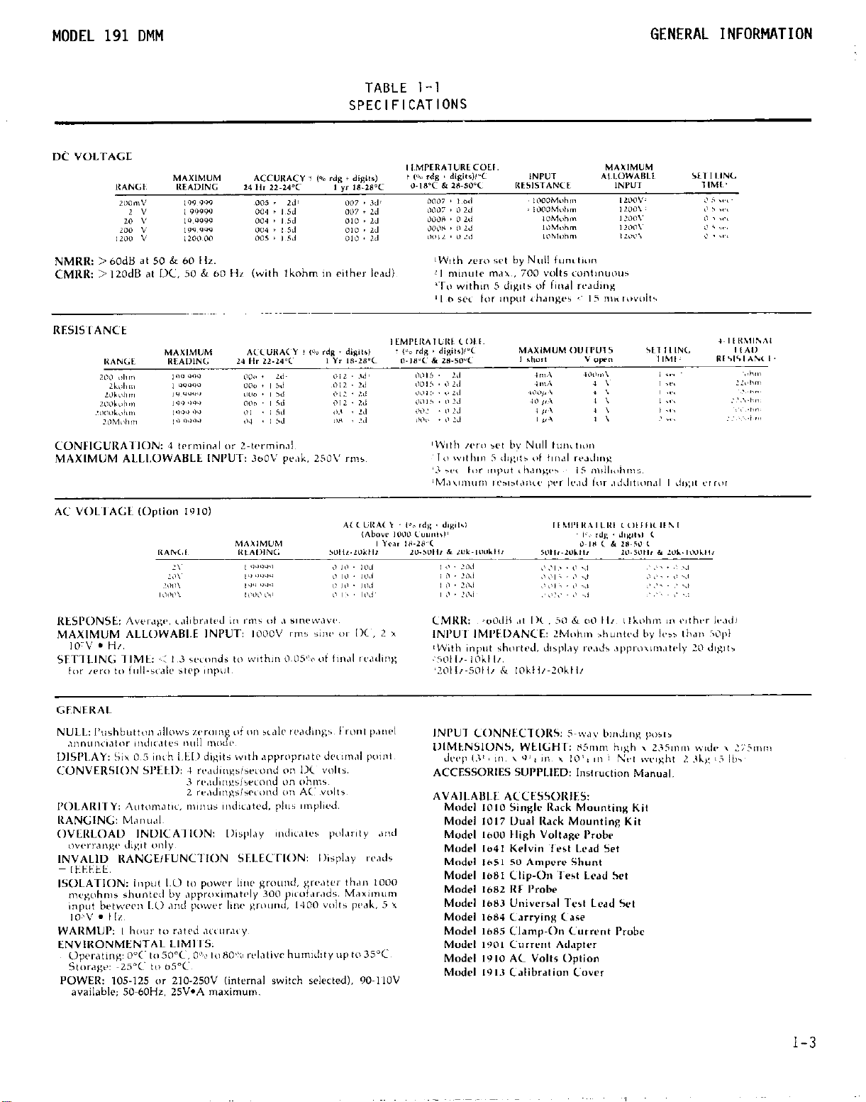
SPECIFICATIONS
Detailed specifications for the Model 191 are
l-2
Page 5
MODEL
191
DMM
GENERAL INFORMATION
TABLE l-l
SPECIFICATIONS
Page 6
OPERATING INSTRUCTIONS
P1006
MODEL
AC OPl
YODEL
191
DMM
e
LINE/FUSE
(F101)
LINE'VOLTAGE
SELECT SWITCH
(S102)
2-o
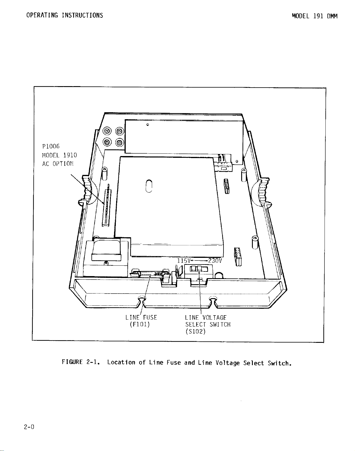
FIGURE 2-1.
Location of Line Fuse and Line Voltage Select Switch.
Page 7
MODEL 191 DMM
~OPERATING INSTRUCTIONS
SECTION 2. OPERATION.
INTRODUCTION.
Z-l.
2-2.
incoming
operation of the Model
2-3.
2-4.
mechanically and electrically before shipment. Upon
receiving the Model 191,
shipping container and check for any obvious damage
which may have occured during transit.
damages to the shipping agent.
original
required.
Model 191 orders:
2-5.
2-6.
on how to connect the Model 191 to your available ac
This section provides information needed for
inspection, preparation for use, and
191 and
UNPACKING AN0 INSPECTION,
The Model 191 was carefully inspected, both
packaging materials if reshipment is
The following items are shipped with all
a. Model 191 OMM.
b. A Copy of this Manual.
Installed or separate optional accessories, as
C.
ordered.
PREPARATION FOR USE.
The Model 191 is shipped ready-for-use on the
line voltage marked on its rear panel. Instructions
line power are contained in Paragraph Z-7 Line
Power.
its accessorieS.
unpack all items front the
Report any
Retain and use the
NOTE
The line voltage sct/tinq of the instrument
is marked on the &r panel. The following
procedure can be uqed to either confirm the
factory setting, or 40 set up the instrument for
operation on another ivoltage range.
voltage range is chdnged, the box next to the
selected line voltaTe should be appropriately
marked as an externalI reminder of the setting.
Use a water soluable barking pen.
Line Voltage Selec~tion.
2-9.
Z-10. Set up the Modejl 191 to operate on your
available ac line voltage as follows:
Turn the DMM botltom side up and loosen the
a.
four screws in the boqtom cover. These sci-ews are
held captive hy rubber O-rings.
Hold the top an?
h.
prevent their separatjon and turn the DMb1 over to
normal position. Rem+, the top cover.
Set switch
c.
line fuse, as indicated in Table 2-1. for your
available input line ~ voltage.
shown in Figure
d. Reinstall the top cover.
8102
2-l.
bottom cover
aind install the proper rated
if the line
together t"
These items are
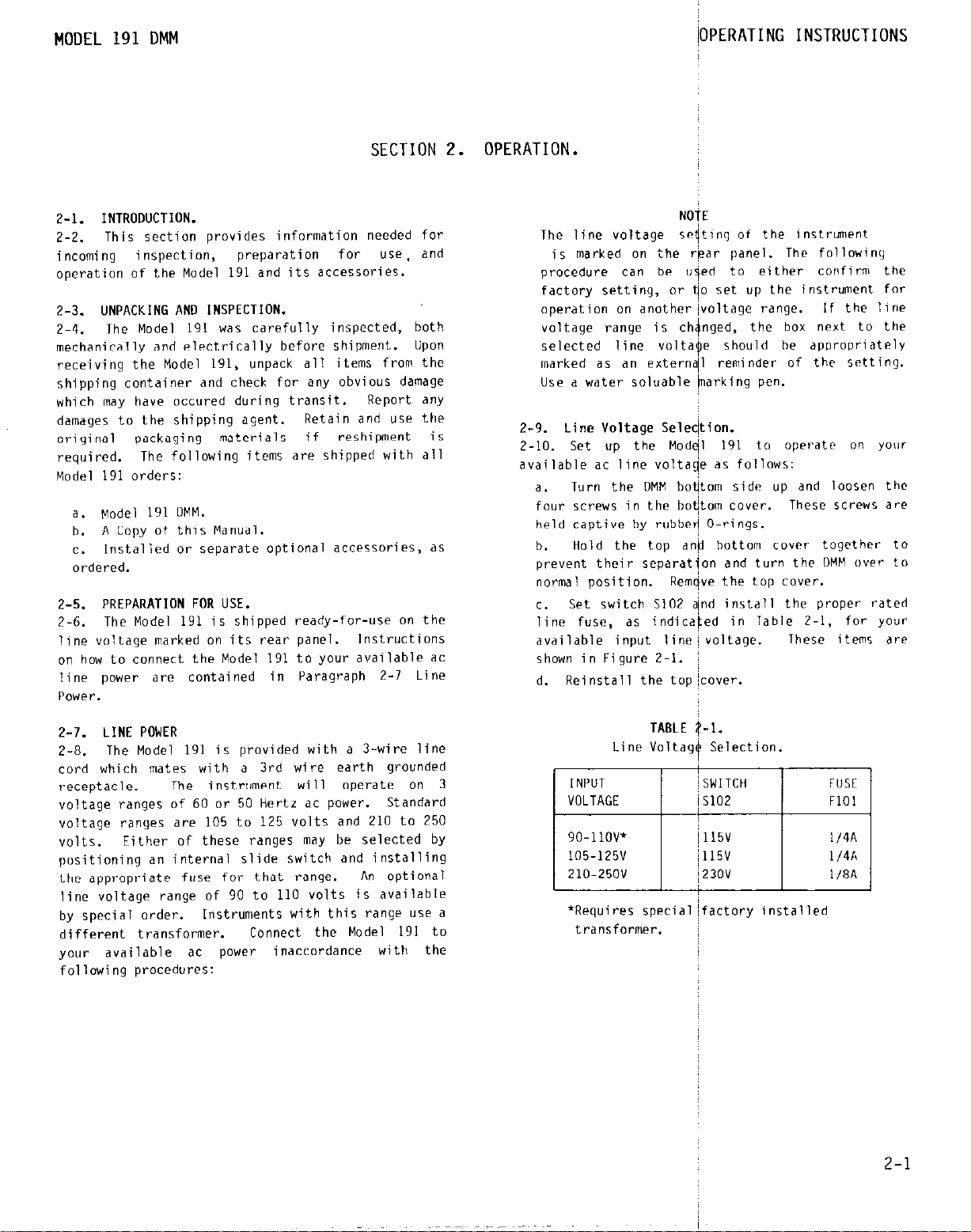
2-7. LINE POWER
2-R.
cord which mates with a 3rd wire earth grounded
receptacle.
voltage ranges of 60 or 50 Hertz ac power.
voltage ranges are 105 to 125 volts and 210 to 250
volts.
positioning an internal slide switch and installing
the appropriate fuse for that range.
your available ac power inaccordance with the
The Model 191 is provided with a 3-wire line
The instrument will operate on 3
Standard
Either of these ranges may be selected by
An optional
line voltage range of 90 to 110 volts is available
by special order.
different transformer.
following procedures:
Instruments with this range use a
Connect the Model 191 to
TABLE 4-l.
Line Voltagq Selection
*Requires special~factory installed
transformer.
2-l
Page 8
OPERATING INSTRUCTIONS MODEL
191
DMM
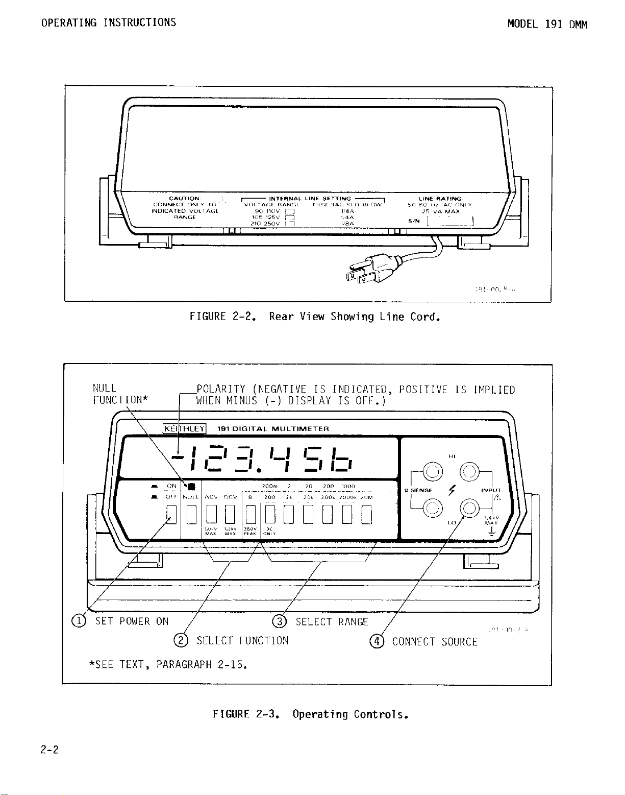
NULL
FUNCTION*
FIGURE 2-2.
POLARITY (NEGATIVE Is INDICATED, POSITIVE Is IMPLIED
rblHEN MINUS (-) DISPLAY IS OFF.)
Rear View Showing Line Cord.
/
2-2
1 SET POWER ON
(I.3
*SEE TEXT, PARAGRAPH 2-15.
I
@j SELECT RANGE
4 CONNECT SOURCE
0'
FIGURE 2-3. Operating Controls.
I", 3 ,.
Page 9
OPERATING INSTRUCTIONS MODEL
2-2
Z-11.
z-12. The Model 191 is provided with a 3-wire line
cord, shown in Figure 2-2, which mates with third-
wire grounded receptacles. Connect the instrument
to ac line power as follows:
2-13. OPERATING INSTRUCTIONS
2-14.
Model 191 [IMM are outlined below, and Condensed
Operating instructions are provided on the bottom
cover of the instrument. These instructions should
only be used after becoming completely familiar with
the operation of the Model
"SC?.
performance and safest operation will be obtained by
using the individual instructions provided in this
section which describe how t" make specific function
mea*"reme"ts.
OMM a5 f0110w5:
Connecting Line Power.
WARNING
\,
Ground the instrument through a properly earthgrounded receptacle before operation. Failure to
ground the instrument can result in sevet-e injury
or death in the event of short circuit or
malfunction. In addition, connect only t" the
line voltage selected. Application of incorrect
voltage can damage the instrument.
Plug the power c"rd into a properly grounded
a.
outlet of a source having the selected line
voltage.
Operate the Model
b.
Paragraph Z-13.
The basic operating instructions for the
Until this familiarity ha5 been achieved, best
Refer to Figure 2-3 and operate the
/&CAUTION
no not exceed the Maximum Inputs limits given in
Table 2-2.
Turn on the power by depressing the ON/OFF
a.
pushbutton.
it is useable immediately, but a 1 hour warmup is
required to obtain rated accuracy.
additional hour may be required from temperature
extrelne5.
Select the function with the ACV, IDCV or n
b.
pushbuttons.
Select the range by depressing the appropriate
c.
pushbutton,
Connect the source to the INPUT terminals and
d.
make the ,n,easurement.
Section 4 should he (used as required.
If the instrument is within 18-2R°C,
191
as described in
191
through day-to-day
up to 1
Accessories described in
Summary of M
UNCTION
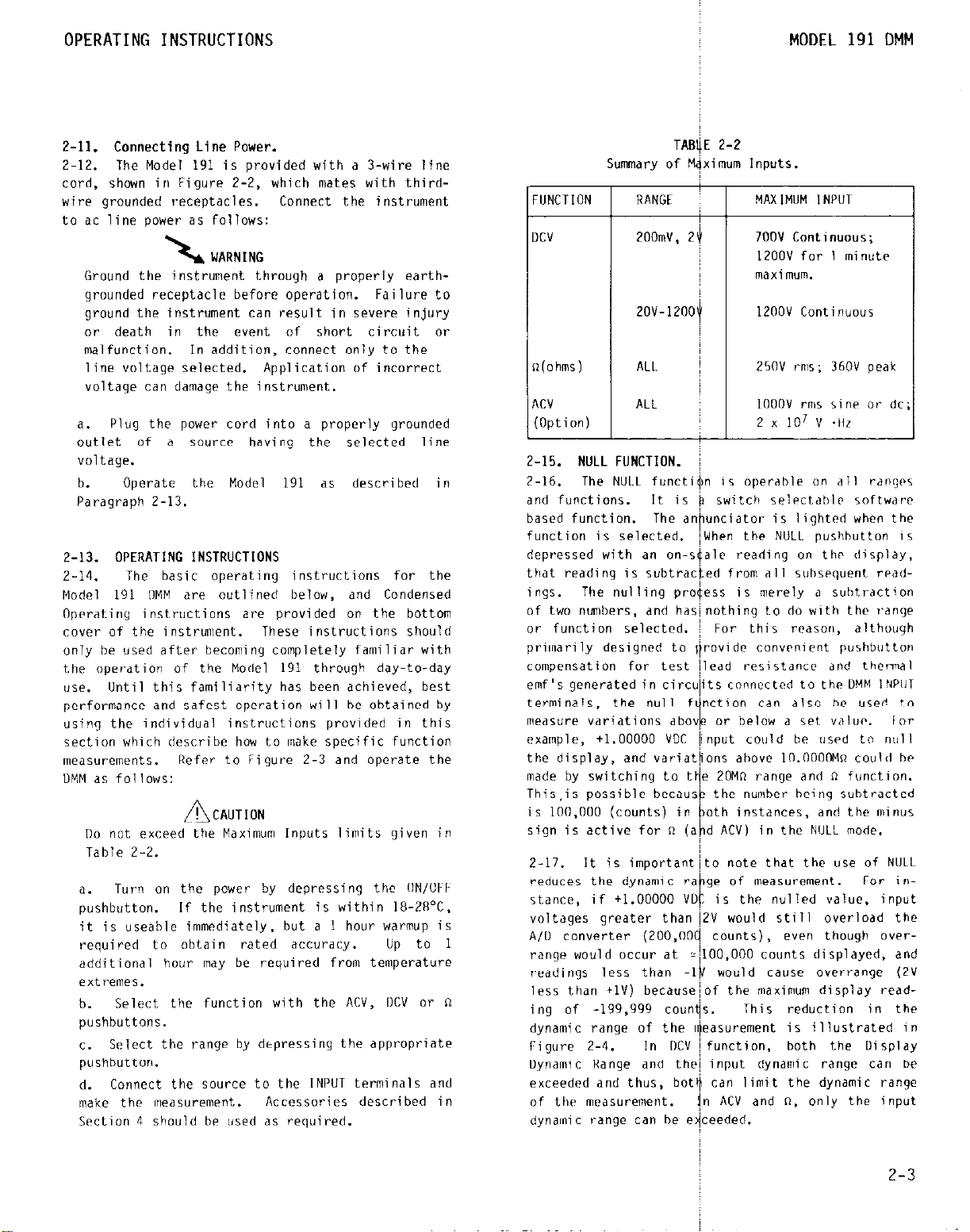
2-15. NULL FUNCTION.
Z-16.
and functions. It is
based function. The dr
function is selected.
depressed with an "n-5
that reading is subtrx
1ngs. The nulling pr"
of two numhers, and ha5
or function selected.
primarily designed to
compen*ation for te5t
emf's generated in circa
terminals,
measure variation5 db"'
example,
the display, and variat
made by switching to t
This,is possible hecaur
is 100,000 (counts) in
sign is active for n (a
2-17. it is important
reduce5 the dynamic re
stance, if
voltages greater than
A,0 c"nverter (200,OOI
range would occur at *
readings less than -1
less than +lV) because
ing of
dynamic range of the
Figure 2-4.
Dynamic Range and the
exceeded and thus, bot
of the meaS"i-erne"t.
dynamic range can be e
The NULL functi
the null f
+1.00000 VDC
t1.00000
-199,999 coun
TAB
RANGE
ZOOmV, 2
zov-1200
ALL
ALL
VL
In ocv
imum Inputs.
MAXIMUM INPUT
7OOV Continuous;
12OOV for 1 minute
Rh3Xllll"lll.
IZOOV Continuous
25OV rms; 360V peak
IOOOV rnis sine or dc
2 x 10⁷ v .Hz
is operable "n all ranger
switch selectdblr software
nciator is lighted when the
?en the NULL pushbutton is
1~ reading on tlw display,
d from all subsequent read55 is merely d subtraction
"thing to do with the range
For this wds"n, althouyh
,vide convenient pushbutton
lad re5istance dnd thermal
s connected to the DMO INPill
:tion cd" also be used t"
or below a 5et valur. 101.
put coutd be used to null
ns ahovc 1O.OOOWO could be
2OMn range and n function.
the numher heing subtracted
th instances, and the minus
ACV) in the NULL mode.
o note that the use of NULL
e of meas"rerne"t.
is the nullpd value. input
I would still overload the
counts), even though "ver-
10.000 counts displayed, and
would cause overrange (2V
f the maximum display read-
This reduction in the
~surement is illustrated in
unction, both the Display
nput dynamic range cd" he
:dn limit the dynamic range
ACV and n, only the input
!eded.
191
For in-
DMM
2-3
Page 10
OPERATING INSTRUCTIONS
199,999
DISPLAY DYNAMIC RANGE
A
/ NULL \
VA&UE
199,999
MODEL
191
MEASUREMENT
DYNAMIC RANGE
IN NULL MODE
(SHADED)
DMM
\
v
INPUT DYNAMIC RANGE
FIGURE 2-4.
Effect of NULL function on Dynamic
Range of DCV Measurement.
Z-18.
described in DC Voltage and n Measurement
Procedures.
2-19.
Z-20. Overrange is indicated by the minus sign
along with the over-range digit and the appropriate
decimal point. All of the remaining less significant digits are blanked. Example:
Overrange is indicated whenever the dynamic range of
DCV measurement is exceeded. With the NULL function
off,
described in Paragraph Z-17, the dynamic range of
the measurement is reduced by an amount determined
by the size and polarity of the nulled signal when
the instrument is in the null mode.
The Use of NULL as pushbutton 'zero" is
OVERRANGE INDICATION.
(-I--.---).
this occurs above
*199,999 CO”“tS. As
/
2-23. DC VOLTAGE MEASUREMENT.
2-24.
microvolt/digit to
displayed reading is 139999. Overrange is indicated
by (-)I-----, except on 1200 volt range. On the
1200 volt range,
maximum allowable input voltage. Maximum allowable
input: 12OOV for
continuous on the 200mV and 2V ranges; 1200 volts
continuous on the ZOV-1200 volt ranges. Use the
Model
The Model 191 reads dc voltages from I
1200 volts. The maximum
the display can read beyond the
I
minute maximum,
191
to measure dc voltage as follows:
CAUTION
A
Do not exceed the maximum allowable input voltage
limits. Instrument damage may occur.
700
volts
2-21.
2-22.
function is selected. These selections are:
2-4
ERROR INDICATION.
-1EEEEE is displayed when an improper range -
ACV function - when AC option is not installed.
20Mn range - with ACV or DCV function selected.
ACV function with 2000, 200mV range selected.
a.
Turn on power with the ON/OFF pushbutton and
depress the DCV pushbutton.
b. Select the desired range from the five ranges
available.
range pushbutton.
by the
The decimal point is positioned by the
The 1200 VDC range is selected
1000
pushbutton.
Page 11
MODEL
c.
off) unless measurements are to be made as
deviations from a preset value.
d.
INPUT HI and LO binding posts. The binding posts
accept wires, spade lugs or banana plugs for ease
of connecting the circuit to be measured. LOW
thermal cabling and connections are recommended
for measurements on the 200mV range.
e.
displayed digits, polarity sign and decimal point
locations.
in volts.
f.
NULL function to obtain rated accuracy. Zeroing
is necessary to compensate for thermal EMF's
generated by the connections to the circuit to be
measured.
microvolts or several tens of microvolts. set
zero as follows:
191
DMM
Ensure that the NULL pushbutton is out (light
Connect the signal to be measured between the
For the top four ranges, merely observe the
The top four ranges are direct-reading
For the 200mV range, ZERO must set with the
These voltages may be only a few
1) Set
2) Disconnect the test leads at the circuit to
be measured and short them.
3) Depress the NULL pushbutton.
4) Reconnect the test lead and make the
measurement by applying the signal and reading
millivolts on the display.
Model
191 to
200mV
range.
g. The optional Mode
be used with the Modt
up to 40 Kilovolts, a
Paragraph Z-30.
2-25.
Z-26.
millioha/diqit to 20
rarqes.
4.wire oh,:6 operation.
sense leads are conmec
natically dew 4-termi
not connected, the me
For 46terminal meax
digit) can be obtaine
log as the maximum 1~
2-3 are mt exceeded.
measurements on the 20
the NULL furrtion to o
RESISTANCE (n)
The Model
The Model 191
191 I
tlodcl 191 to measure 7
&CA"
MAXIMUM ALLOWABLE I
36OV peak, 25UV rms
voltage.
a. Turn on power and
h. Connect the circ
INPUT terminals and I
the six ranges avail
positioned by the ran
Instrument
IOPERATING INSTRUCTIONS
1600
High voltage Probe can
191 to measure
reduced accuracy. Refer to
JASUREMENT
IN ~nedsures resistdrre fron 1
eqohms.
prwides d~tondt>c 2-wit-e or
This nedns that if the ohms
ed, the rneasurcment IS autoIal if the sense leads are
iureiaent is done 2.terminal.
eme nts
on the top five rarqes as
ION
'UT VOLTAGE (all ranges):
Do not exceed maximum
amage may occur.
depress n pushbutton.
lit to be measured to the
,lect the desired range from
ble.
e pushhutton.
SEC Table 2-3 for
rated
The decimal point is
dc voltages
dCC"l'dCY (tl
TABLE 2-3
Resistance Ranges
RANGE
SETTING
200 n***
2k n
20k n
200k n
2000k "
20M n
MAXIM""
READING
199.999
1.99999
19.9999
199.999
1999.99
MAXIMUM OUTPUTS'
I(Shorted) V(Openl
-4mA -4OOmV 7n
-4mA -4V 22"
-4OOuA
-4OuA
-4uA -4v 7000
1g.gggg t-““-
OVERRANGE: MAXIMUM
-l---_
* HI binding post (red) is negative.
** Maximum resistance per lead for additional
l
** Zero must be set by NULL to obtain rated accuracy.
1
digit en-or.
.,
-4v
-4v
-4v
ALL RANGES
-r
ALLOWABLE
360Vpeak,
MBX.
2200n
INPUT:
4-w,
700
22on
;*
250Vrms
2-5
Page 12
OPERATING INSTRUCTIONS
MODEL 191 DMM
For 4-terminal measurement c"nnect the sense
c.
leads t" the circuit t" be measured and to the n
SENSE terminals on the 191. This arrangement
eliminates the err"r due to the voltage drop
across the current-carrying leads.
d. Ensure that the NULL pushbutton is out (light
off) unless measurements are to be made as
deviations from a preset value.
c. For the top five ranges of Z-wire or 4-wire
measurements, merely observe the displayed digits
and decimal point to make the measurement.
f. For d Z-wire or 4-wire ohms imeasurement on the
200n ra"qE,
function to obtain rated accuracy.
necessary to colrlpfnsate for test Icad resistance
On Z-wire & Thermal Emfs on 2 & 4-wire.
as follows:
1) IDisconnect the test leads at the circuit to
be rmeasured, and short them.
2) ocpress NU,.L p"shb"tt"n.
3) iReconnect the test leads and <make the
IIIEaSIItm!x!"t.
g. "iodf Test.
diode testinq.
resistance Of J
approximately 190n. (Hiqh Terminal is Negative)
Z-27.
OPTION).
2-28.
reads ac voltages from 10 microvoltsldigit to 1000
lCK0 rmust be set with the NULL
Zeroing is
set LPr"
Thr 2Kn range is rccomxnded for
On this range the forward oil
silicon diode
Ac VOLTAGE MEASUREMENT (WITH 1910 AC
With the Model 1910 option, the Model 191
will read
volts. The instrument is avera9e responding and
displays the root !:ledo square
with a frequency of 50Hr t" 100kllr. Accuracy is
specified for 1000 counts and above. The maximum
reading is 199999. Overrange is indicated by (-)
i-----, except on 1000 volt range. On the 1000 volt
range,
allowable input voltage. Maximum allowable input:
IOOOV r‘ms or dc; 2 x lO'V.tir. "se the Model 19,
to "leasure dC voltage as follows:
a. Turn on power with ON/OFF pushbutton and
depress the ACV pushbutton.
h.
available. The decinlal point is positioned hy the
range pushbutton.
C.
off) ""less measurements are to
deviations front a preset value.
the display can read beyond the lmaximum
/!&CAUTION
Do not exceed maximunl allowable input voltage.
Instrument damage may occur.
Select the desired range from the 4 ranges
insure that the NULL pushbutton is out (light
NOTE
Do not use NULL to zero Lhe range.
residual zero reading is normal (approx. 20tiuV)
If NIJLI. is used to zero this offset. reailirlgs in
specified accuracy range wili be 1"~ by the
offset amount.
d. Connect the signal to be measured between the
INPUT Ill and LO binding posts.
accept wres,
of connecting the circuit to be measured. Observe
the displayed digits and decimal point.
e. The Model 1682 RF Probe can he used with the
Model 191 to measure 0.25V to 30V rms ac signals
with a frequency IOOkHr to IOOMHr (and above at
reduced accuracy). Refer to Paragraph 2-36.
spade lugs or banana plugs for ease
value Of a 51~ W~VC
he Imade as
A Sllldll
The hinding posts
2-6
Page 13
MODEL
191
DMM
SECTION 3 PERFORMANCE VERIFICATION.
3-1.
GENERAL.
Performance verification may be performed upon
3-2.
receipt of the instrument to ensure that no damaqc
or nisadjustment has occurred during transit. Verification may also be performed whenever there is
question of the instrument's accuracy, and following
calibration, if desired.
NOTE
For instruments that are still under warranty
(LESS than 12 month5 since date of shipment),
if the instrument's performance falls outside
specifications at
Keithley rcpresentativc or the factory iomediate1y.
3-3. RECOMMENDED TEST EQUIPMENT.
3-4. Kecommended test equipment for performance
verification is listed in Table 3-1. Alternate test
equipment nay be used.
the alternate test equipment is not at least 3 tines
better than the instrument specifications, addition-
al allowance must be made in the readings obtained.
Some of the equipment listed in Table 3-l is not 3
times better than the 191 specifications because
such equipment is not readily available. In these
instances, the verification procedures indicate the
equipment manufacturer's specified uncertainty, and
include the uncertainty in determining the allowable
rcadiny for the Model 191.
any point,
However, if the dccuracy of
contact your
PERFORMANCE
VERIFICATION
3-5. ENVIRONMENTAL COND1TIONS.
All neasurenents slhouid be made dt a" dnbirnt
3-6.
tenpcraturc within the rpnge of 18' to 28°C (65" to
82Or). and a relative hu#idity of lcsr thdri 80%.
3-1. PERFORMANCE VERIFI$ATION PROCEDURE.
3-K.
basic accuracy of the Moidfl Ill DI,!M for dc voltnge.
resistance and dc voitagc (rrlth l.lodei 1910 AC
Voltage Option installdd) 1mcd5urcnwnts. it thP
instrument is out Of s~pecificdtion at Jny po,nt,
perfor,, a complete ca)ibration a5 d,xc,.ibv! in
Section 6,
wavva"ty, as noted above.
3-9.
Use the f"llowin(i procedures to verify the
~nlcss the :instrwwnt 15 still iindrr
NOTE
Performance verificbtion should bc pcrfonncd by
qualified pcrsonnel~ using accurdtc and rcliablr
test eq"lpncnt. ~
initial Conditions;
Recommended Test Equipment For Performance Vcrifica
T
ITEP
DESCRIPTION
-
A
DC Calibrator
8
AC Calibrator
C
High Voltage Amplifier
(Used with Model 745A)
"
IIccade Resistor
E
Kelvin-Varlcy Voltage
Uivider
(Used with Model 343A)
TABLE 3-l.
SPECIFICATION
190n, 1.9kn,19kil,
190k0,1.9Mn, lOMn,
t0.017,
.19v, 1.9v
with .2ppm Terminal
Linearity
tilot
1.
72OA
3-l
Page 14
PERFORMANCE
VERIFICATION
MODEL
191
DMM
b. Turn on the Model 191 and allow it to wdrrl up
for one hour.
WARNING
Sonc procedures require the USC of hi9h voltage. Take cat-c to prevent contact with live
circuits which could cause electrical shock resulting in injury or death.
3-11. DC Voltage Accuracy Check ('ZOV to 1ZOOV
R‘?"%? Applied Allowable Readings at 18O to 28'C
I I
I 4
I
3-12. DC Voltage Accuracy Check (200mV and 2V
Ranges).
4. Select dc voltaqe function.
h. Connect the DC calibrator (Item A, Table 3-l)
to the instrument.
c. Select the 2flV range, and apply positive 1OV
dc to the DMM. The readin &st be within the
limits specified in Table 3-2.
Select each rcnaining range and apply r-c-
!i.
quircd voltage specified in Table 3-2.
that the reading is rrithin specifications.
f. Repeat all checks with negative voltage.
DC Voltaqc Performance Check (2OV to 12OOV Ranoc).
Voltage
I
Ranges).
2. Sclcct DCV and 200mV range.
b. Disconnect test leads at the DC calibrator
(A) and short them.
Ibutton. Verify a display indication of OO.OOOmV
+O.OOlnV flashin9.
t
I
TABLE 3-2.
99.986 to 100.014
999.86 to 1000.14
9.9986 to 10.0014
Depress the Model 191 NULL
Verify
c. Connect the DC calibrator (A), Kelvin-Varley
Voltage Divider (E) and Model 191 as shown in
Fi9urc 3-1.
.0190000 output.
Temporarily disconnect the test leads from
i,
the DC calibrator (A) and short them.
Model 191 PlULL button for a display indication of
00.000 ~OO.OOLmV flashing.
c. Reconnect the DC calibrator (A) and set to an
output Of +10.00000V.
f. Verify that the Model 191 reading is between
t189.978 to t190.022nV. Note that the allowable
reading includes a 6 digit allowance for the
uncertainty of the DC calibrator (A) and Voltage
Divider (E).
~9~. Kopfat step d thru f with negative voltage.
h. Select the 2V range and rcleasc the NULL
button. Set the Kelvin-Varlcy Voltage Divider
(E) to .I90000 output.
1. Verify that the Model 191 reading is between
t1.89981 and t1.90019V. Note that the allowable
reading includes 24 digits for DC calibrator (A)
uncertainty.
i. llfpeat step i with negative voltage.
3-13. AC Voltage Accuracy Check (With Model 1910
I
1
AC Voltage Option Installed).
A. Select ac voltage function.
b. Connect the AC calibrator (Item R, Table 3-1)
to the DMM. Set the calibrator frequency to IkHr.
2. Set the DMM to the 2V range and apply IV ac
to the DMM. The reading must be within the
limits specified in Table 3-3.
Select the 20 and 200 volt ranges and apply
d.
the required voltages as specified in Table 3-3.
Verify that the readings are within specifi-
Set the voltage divider (E) for
DepESS
3-2
DC
Calibrator
(A)
+
OUT
FIGURE 3-l.
1.0
HIGH,
Kelvin -
Varley
LOW
Voltage
LOW
Divider
(El
Test Circuit For 2OCmV And 2V Accuracy Check.
MODEL
191
Page 15
MODEL
191
DMM
PERFORMANCE
VERIFICATION
To check the 1000 volt range, connect the
2.
High Voltage Amplifier (Item C, Table 3-l) to the
output of the AC calibrator per the manufacturer's instructions. Connect the amplifier
output to the Model 191 INPUT terminals. Set the
AC calibrator for amplifier output of 1000.00
volts at lktlz. Verify that the DMM reading is
within the specified limits in Table 3-3.
TABLE 3-3.
AC Voltage Accuracy Check
Range Applied
Voltage
Allowable Readings
at 18’= to 28’C
at
2:;
2oov 1oo.oov
1ooov
10 1 .ooov .ooov
1ooo.ov
9.9868 .99868 to to 10.0132V 1.00132V
99.068 to 100.132V
998.00 to 1002.00v
m
2ov 1o.ooov
at 20ktlz
2ov 1o.ooov
at 100kHr
9.9868 to 10.0132V
9.9868 to 10.0132V
2ov 1o.ooov 9.90 to 10.10
L
f. To check accuracy /at 5OHz. ZOktlz, and lOOkliz,
select the 20 volt ;ranqe, apply the voltage
specified in-Table 3-13 at 5011z, then repeat at
20kHz and 100kHz.
are within the specifiied limits.
3-14.
Resistance (n) Accjuracy Check.
5. Select resistancejfunction by depressing the
R pushbutton.
0. SeleCt
C.
3-I) to the DMM.
L!.
sate for lead resist+xe by depressing the IiuLL
for a display indicition of 00.000
flashing.
Set the decade rjsistar to 1900. Verify that
J2.
the reading for the! 200n range is within the
limits specified in Tbblc 3-4.
f. Select the Zkr! rpngc.
Set the decade rcpistor to LC~O and reset the
9.
NULL.
h. Set the decade rbsistor to 1.900kn.
that the reading is bithin the limits spc!clfiCd
in Table 3-4.
L. COntiNE by uSin the NULL to eliminate lead
resistance on each ra'ngc and measure the next rcsistance as specifiei in Table 3-4. Test each
item in the table andi verify that each wading is
within specificationsi.
200n rc3ngfi
Connect the decape resistor (Itw 0. Table
Set the decade rjsistor to zero and comp~n-
Veinfy that the DMkl readings
~
* 00.301
vwify
TABLE 3-4.
Resistance Accuracy Check.
RANGE RESISTANCE
zoon 190n
2kn
20kn 19.00 kn
200kn
2000kn
20Mn
* Manufacturer's specified uncertainty of the decade resistor (D)
This uncertainty has been added to the specified accuracy of the
obtain the allowable reading.
1.900 kn
190.00
1900.0
kn
kn
10.000 nn
ALLOUABLE READING AT 18' to 28'C
189.955 to 190.045ri
1.89956 to 1.90044 kn
18.9956 to 19.0044
189.956 to 190.044
1899.22 to 1900.78
kn -p
kn 219 diqits
kn
9.9908 to 10.0092 Mn
~ *
,
?I9 digits
219 digits
+ 9 digits
?(19
digits
410
digits
3-3
Page 16

Page 17
MODEL 191 DMM
ACCESSORIES
SECTION 4.
4-1. GENERAL.
This section describes the various accessories
4-2.
and options available for use with the Model 191
DMM.
4-3. LINE POWER OPTION.
The Model 191 can be powered by a line voltage
4-4.
of 90 llOV, 50 - 60Hz with the special factory
installed transformer option.
available by ordering a Model
- 60Hr).
4-5~ MODEL
4-6.
has a
on the DMM corresponds to 1 kilovolt.
TO operate:
Volt range.
1600 to the INPUT terminals.
gator clip on the Model 1600 to source low. Connect
the probe tip to source high.
Specifications: Voltage Rang
40,000 volts DC.
Input Resistance:
1000
Division Ratio:
Ratio Accuracy
+1.5% at Z!ikV, decreasing to
fZ.fl% at 20kV and 30kV
f3.0% at 1OkV and 4OkV, and
+4.0% at 1kV.
Ratio Stability:
Heating Effects: Self-heating due to application of
high voltage for period in excess of 1 minute will
cause a maximum of 0.2% additional error at 40kV
(error is less at lower voltage).
4-7 . MODEL 1651 50-AMPERE SHUNT
4-8. The Model
be made from 0 to 50 amperes DC and from
50 amperes AC with AC Voltage option.
O.OOlohm
current will correspond to 50 millivolts.
To operate: Connect separate CUTrent leads (not furnished) between
the source and the Model 1651 hex-head bolts.
leads that are rated up to 50 ampere capacity.
Connect the voltage leads (furnished) between the
Model 1651 screw terminals and the DMM INPUT
1600
HIGH VOLTAGE PROBE.
The Model 1600 extends the DMM to 40kV. It
1OOO:I
division ratio which means that 1 volt
Set the DMM to OCV and 200
Connect the banana plug on the Model
imegohms.
1OOO:l.
tO.Ol%
1651
kl%
4 terminal shunt.
per "C;
allows current measurenlents to
This option is
191 DMM (90 IlOV, 50
Connect the alli-
eO.l%
per year.
10 t0
It is a
A fifty ampere
Use
ACCESSORIES
terminals.
DCV and 200 millivolt iange.
on DC 200mV.
4-9.
4-10.
leads 1.2~1 (48 inches) 1 ng, terminatedY p
with banana plug and spri,ng-action clip-on
probe.
4-11. MODEL 1682 RF
4.12. The Model 1682 ex
voltage response of the
lOOkliz to lOOMHz,
To Operate:
and 200 Volt range.
to the DMM INPUT termina
Specifications:
Voltage Range: 0.25 to
Transfer Accuracy:
peak responding calibr ted in rms of a
sinewave.
Input Impedance:
Maximum Allowable Input:1 30V pms AC. 2OOV UC.
Accessories Supplied: shraight tip. hook tip,
ground clip, hi adapt+, banana plug adapter.
4-13.
4-14.
long with 12 screw-in tips - 2 banana
plugs, 2 spade lugs. 2 alligator clips ,I\
with boots, 2 needle ti
and 4 heavy duty tip plugs.
4-15.
4-16.
vinyl case with a fitte
insert with room for the Servic
Manual and small access+ies.
4-17.
4.18.
clamping onto a single conductor.
the current path is unngessary.
detects current by sensilng magnetic field produced
by current.
To Operate: Set the OM
volt
Set the DMlj to ACV and 2V range or
MODEL
1681
CLIP-04 TEST LEA0 SET
The Model
NODEL 1683 UNIVERbAL TEST LEAD KIT.
Two test leads, 11.2m (48 inches)
Model 1684 Carrying Case
The Model 1684 is a hard
MODEL 1685 CLAMP-ON AC CURRENT PROBE.
The Model 1685 "edsure~ AC current by
range.
1681 CO tdins two
Set the DMM~to DCV
Connect t/he Model 1685 to the DMM
!
"SC NULL to zero
PRO
Con ect the Model 1682
5.
1
0 volts rms.
to.5 B, 1OOkHz to 1OoMtlZ
1
4 megop shunted by 3pF.
s with chucks
v
foam
1
Interruption of
The Model 1685
to ACV and 20
4
/I"
f! J
A
\
/
i
4-l
Page 18
ACCESSORIES
MODEL
191
DMM
INPUT terminals. The DMM will display 0.1
volts per ampere.
Specifications:
Range: 2, 20
and 200
amperes r-m.
Accuracy: i-4% of range at
60Hz. ST% of range at 50Hz.
Temperature Coefficient:
200 ampere range.
range.
Maximum Allowable Current: 300 amperes rms.
Maximum Conductor Voltage: 600 volts rms.
Conversion Ratio: 0.1 volt rms per ampere.
4-19.
4-20.
with overall dimensions 5-I/4 inches (133mm) high
and
MODEL
1010
SINGLE RACK MOUNTING KIT.
The Model
19
inches (4l33mm) wide.
1010
?O.O5%/"C an the 20 and
*0.3%/Y on the 2 ampere
is a single rack mounting kit
4-25.
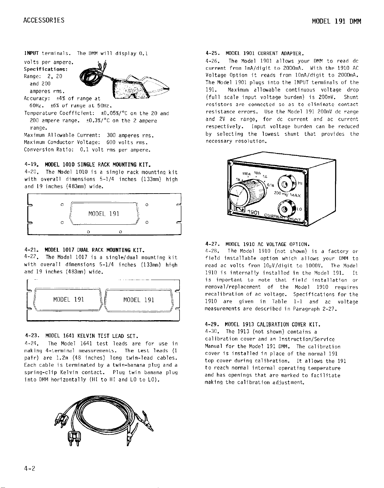
4-26. The Model 1901 allows your DMM to read dc
current from 1nAldigit to 2000mA. With the
Voltage Option it reads from lOnA/digit to 2000mA.
The Model 1901 plugs into the INPUT terminals of the
191.
(full scale input voltage burden) is 200mV. Shunt
resistors are connected so as to eliminate contact
resistance errors. Use the Model 191 200mV dc range
and 2V ac range, for dc current and ac cut-rent
respectively. Input voltage burden can be reduced
by selecting the lowest shunt that provides the
necessary resolution.
MODEL
1901
CURRENT ADAPTER.
1910
Maximum allowable continuous voltage drop
AC
4-21. MODEL 1017 DUAL RACK MOUNTING KIT.
4-22.
with overall dimensions 5-l/4 inches (133mm) high
and
4-23. MODEL 1641 KELVIN TEST LEAD SET.
q-24.
making 4-terminal measurements. The test leads
pair) are 1.2m (48 inches) long twin-lead cables.
Each cable is terminated by a twin-banana plug and a
spring-clip Kelvin contact. Plug twin banana plug
into DMM horizontally (HI to HI and LO to LO).
The Model 1017 is a single/dual mounting kit
19
inches (483mm) wide.
The Model
1641
test leads are for use in
(1
4-27.
4.28. The Model 1910 (not shown) is a factory or
field installable option which allows your DMM to
read ac volts from IOuV/digit to 1OOOV.
1910 is internally installed in the Model
is important to note that field installation or
removal/replacement of the Model
recalibration of ac voltage.
1910 are given in Table 1-l and ac voltage
measurements are described in Paragraph 2-27.
4-29. MODEL
4-30.
calibration cover and an Instruction/Service
Manual for the Model 191 DMM. The calibration
cover is installed in place of the normal 191
top cover during calibration.
to reach normal internal operating temperature
and has openings that are marked to facilitate
making the calibration adjustment.
MODEL
The
1913
1910
AC VOLTAGE OPTION.
1913
CALIBRATION COVER KIT.
(not shown) contains a
The Model
191. It
1910
requires
Specifications for the
It
allows the 191
4-2
Page 19
MODEL 191 DMM
SECTION 5. THEORY OF OPERATION
GENERAL
5-l.
5-2. This section contains circuit descriptions for
the Model 191 DMM and the Model
option.
description of overall instrument operation, followed by descriptions of individual functional circuit blocks. To facilitate understanding, the descriptions arc keyed to accompanying simplified block
and schematic diagrams. Detailed schematics. of the
Model 191 and Model 1910 are provided in Section
1.
5-3.
5-4.
count, bench DMM with 5 dc voltage and 6 resistance
ranges standard. It has luV and Inn sensitivity, and
The information is arranged to provide d
OVERALL FUNCTIONAL DESCRIPTION
The Model 191 is a 5.112 digit, ~200,000
1910
AC Voltage
THEORY OF OPERATION
0.00052 resolution. Whe
tion is installed, ac
1000 volts can be "leas"
of the Model 191 is
converter which uses b"
slope conversion techni
control of the microcc
high conversion speeds
some of the Imajor bcnef
Other benefits and func
to the use of the micr(
the number of componer
filtering; pushbutton n
signal; and automatic 2
will bc described 1n
sectlo".
,.“, “.-..J
MODEL 1910
AC VOLTAGE
DCV ATTENUATOR/n
REF. RESISTORS
& RAFIGE SWITCHING q
ACV
O--I- n
ACV
ACV
f2
COE'VERTEI
VZERO
VSIG
A/D
VREF
57+
V/F
PULSES,
cnw.0111
PICRO-
COMPUTER
DISPLAY
FIGURE 5-l.
Simplified Signal Flow Block Diagram, Mod.
41
191
cl
DMM.
5-1
Page 20
THEORY OF OPERATION
MODEL
191
DMM
(b) Timing.
loome‘
--I t-
Inteqratian_Ph_asej Vsig 1 Vzero I Vsig
Reading Updates
FIGURE 5-2.
Block Diagram of DC Voltage Measurements.
200msec
Charge-Balance
I Vref I Vsig I
in
vrero ----
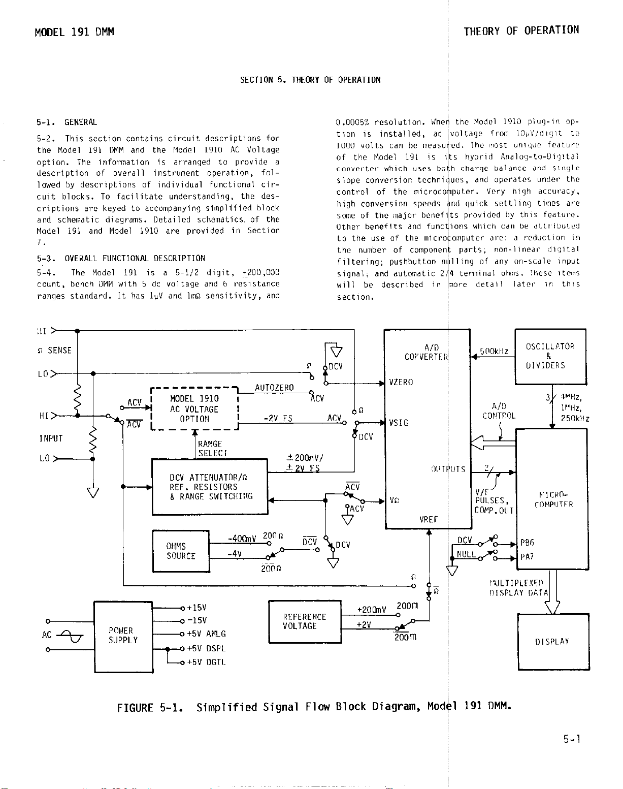
Figure 5-1 provides a simplified signal flow
5-5.
block diagram of the Model 191.
tioned,
around the A/D converter, operating under the control of the nicrocomputer.
designed to handle input signals up to t2 Vdc, and
up to four separate signals (i.e., VLEKO, VSIG, Vn
and VREF).
the function switches control which of the siqnals
that can be applied to the A/D convcrtcr, as well
as the signal conditioning path of the input signal
applied to the input terminals. The microcomputer,
through the A/D Control lines, controls the sfquence and timing of signals applied to the A/D
converter.
second integration period for the charge balance
phase of conucrsion, up to 1 millisecond for single
slope conversion and the necessary delays to allow
an input signal to Settle and to perform nathema-
5-2
operation of the Model 191 is centered
It can be seen from the diagram that
Timin includes a precise 100 milli-
As previusly men-
The A/D converter is
tical calculations and housekeeping chores.
microcomputer also provides the automatic zero and
automatic calibration corrections to eliminate zero
and gain errors frown the signal to be displayed.
This is done mathematically and requires that more
than just VSIG be converted. Three signals are required for dc voltage mesurements, and four signals
for ohms and JC volts. Lath signal required for
the wzas~~rement is applied to the A/D converter and
the resulting digitized value is stored in ~memory.
The microcomputer muses the stored values to calcu-
late the reading and sends it to the display. In
this way, the microcamputcr corrects for zero and
gain errors, arId the displayed reading is the digitized value of the input signal within the specified accuracy of the
instrument.
The
Page 21
MODEL
191
DMM : THEORY OF OPERATION
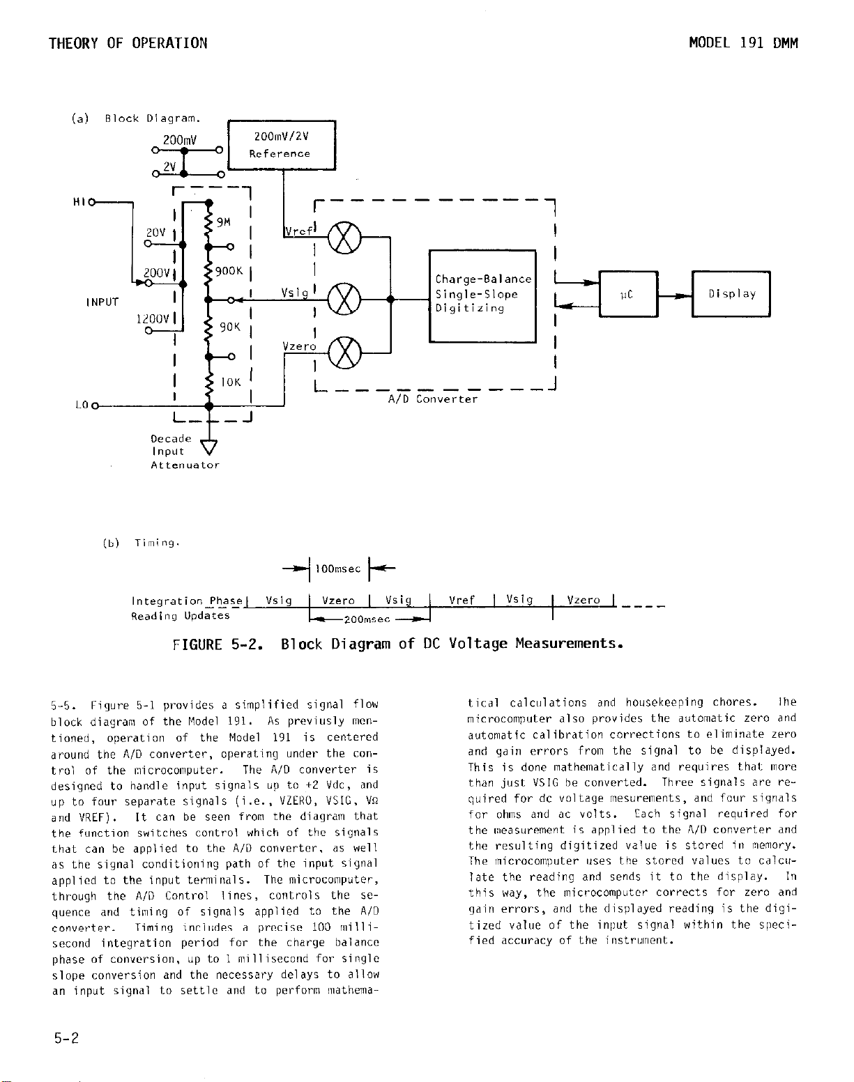
5-6.
DC Voltage Measurement.
5-7.
5-2, the input signal either goes directly to the
A/D or is connected across a decade attenuator with
a total resistance of 10 megohms. The attenuation
of the dc input signal is determined by the range
selected.
signals to the A/D converter arc rcquircd for dc
volts operation (i.e.,
signal is presented to the AID input and (measured
for 100 milliseconds (See A/D Converter discussion). Each digitized value is stored in memory and
then used to calculate a reading by the formula:
In dc volts operation, as shown in Figure
As previously mentioned, three input
"SIG, "ZERO and VREF). Each
(a) BLOCK DIAGRAM
-4oomv/-4V
Voltage
SO"rCe
r- --i
eference Resistor Decade
It can be seen that
tracted from both the
then the ratio is ti
needed because the r
milllivolts on the loti
5-R.
gram, VSIG is medsure
and VREF are alternati
This permits the disp
two integration (char!
ing that up to an addi
required (to complet
counting of the remail
tic.31 computations),
made approximately (
approximately 4 read'
As shown in th
the zero error is sub-
II and the reference, and
Multiplication by 2 is
nce is 2 volts (or 200
ic range).
ling portion of the dia'ry other time dnd VZtRO
in the other tine slots.
3 be updated after every
am?) phases. Consider11 70 milliseconds nay bc
Igle slope conversions.
in counters and mathcmaI display update cdn be
210 nilliseconds, or
;econd cd" be obtsined.
%
(b)
TIMING
9 IOOms /---
INTEGRATION PHASE 1 DELAY 1
READING UPDATE
FIGURE 5-3.
Block Diagram of Resistance Measureme:
VSIG 1 VLEKO DELAY
cl
'0 VKEt
_.
4
n%.
5-3
Page 22
THEORY OF OPERATION
MODEL 191 DMM
5-9. Resistance Measurement.
5.10. In ohms operation, as shown in Figure 5-3,
the ohms voltage source is connected as an input to
the A,0 converter and to one end of the reference
resistor decade. The resistance reference resistors
are the same resistors that are use for dc volts
attenuation, but unlike dc volts, where only the
ratios affect accuracy, the absolute characteris-
tics of the resistors determine accuracy of the
ohms measurement. The value of the ohms reference
resistor (Itn) is determined by the range selected.
An ohms source voltage of -400 millivolts is used
on the 200~2 range, and -4V is used for all other n
ranges.
signals to the A/D converter are required. Each
signal is measured for 100 milliseconds and its
diyitirec value is stored in memory. The microcomputer then calculates a reading using the formula:
It can be seen that "$2 - VKEF is the voltage across
Kn (Ifi X rtn) and that "SIG VZEKO is the volt-
age acrossRX ('n X i(X). therefore:
For resistance measurements, four input
nD,SP = vslc - VZEKO
vn VREF
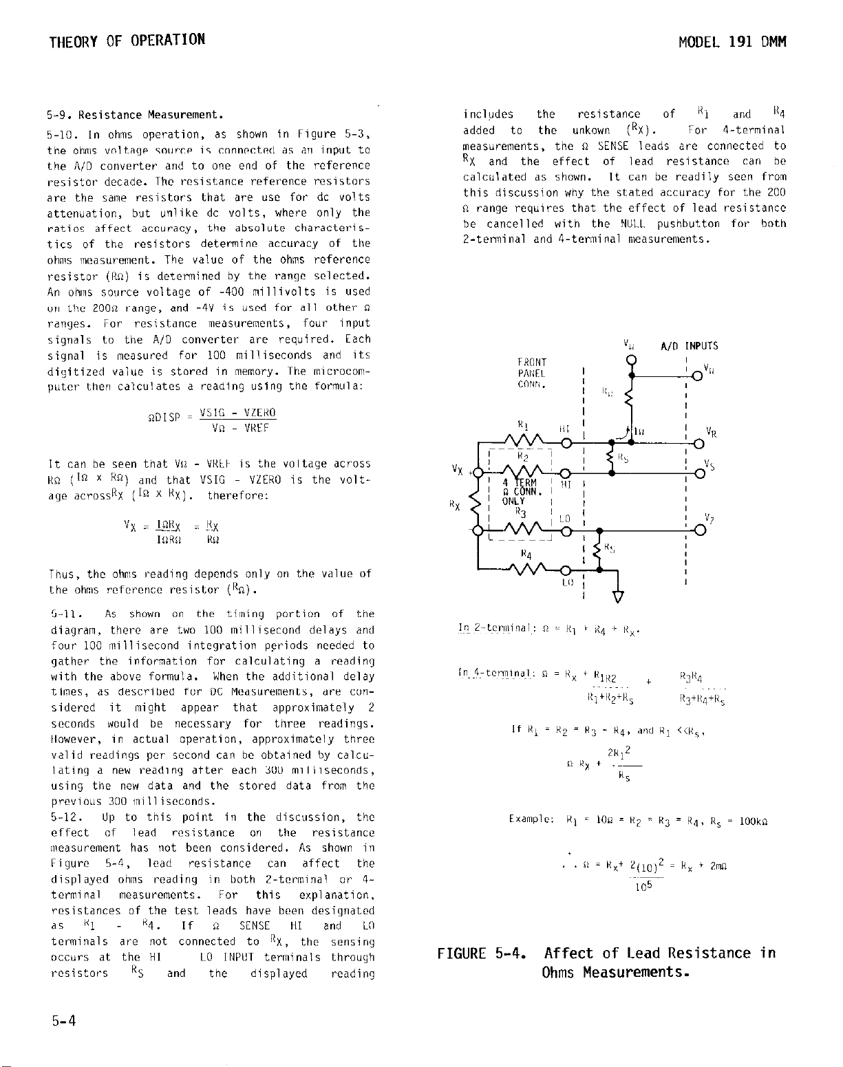
includes
added to
,"easurt3"ents,
RX and the effect of lead resistance can be
calculated as shown.
this discussion why the stated accuracy for the 200
n range requires that the effect of lead resistance
be cancelled with the NULL pushbutton for both
Z-terminal and &terminal measurements.
the rESlSta"Cf of RI
the unkown (RX). For &terminal
the n SENSE leads are connected to
It can be readily seen from
and 'I4
Thus, the ohms reading depends only an the value of
the ohms rcfcrfncf resistor ("n).
5-11.
diagram, there are two 100 millisecond delays and
four 100 millisecond integration p?riods needed to
gather the information for calculating a reading
with the above formula.
times, as described for DC Measurements, are considered it might appear that approxilnately 2
seconds would be necessary for three readings.
IloWeYfr, in actual operation, approximately three
valid readings per second can be obtained by calcu-
lating a new reading after each 300 milliseconds,
using the new data and the stored data from the
previous 300 milliseconds.
5-12. Up to this point in the discussion, the
Effect of lead
n~easurement has not been considered. As shown in
Figure
displayed ohms reading in both Z-terminal or 4terminal meas"rements.
resistances of the test leads have been designated
3s '31 @4. If n
terminals are not connected to Rx, the sensing
occurs at the HI
rfsistors
AS shown on the tilning portion of the
When the additional delay
resistance an the resistance
5-4,
lead resistance can
For this explanation,
SENSE HI
KS
LO INPUT terminals through
and
the displayed
affect the
and LO
reading
FIGURE 5-4. Affect of Lead Resistance in
Ohms Measurements.
5-4
Page 23
MODEL
191
DMM
THEORY OF OPERATION
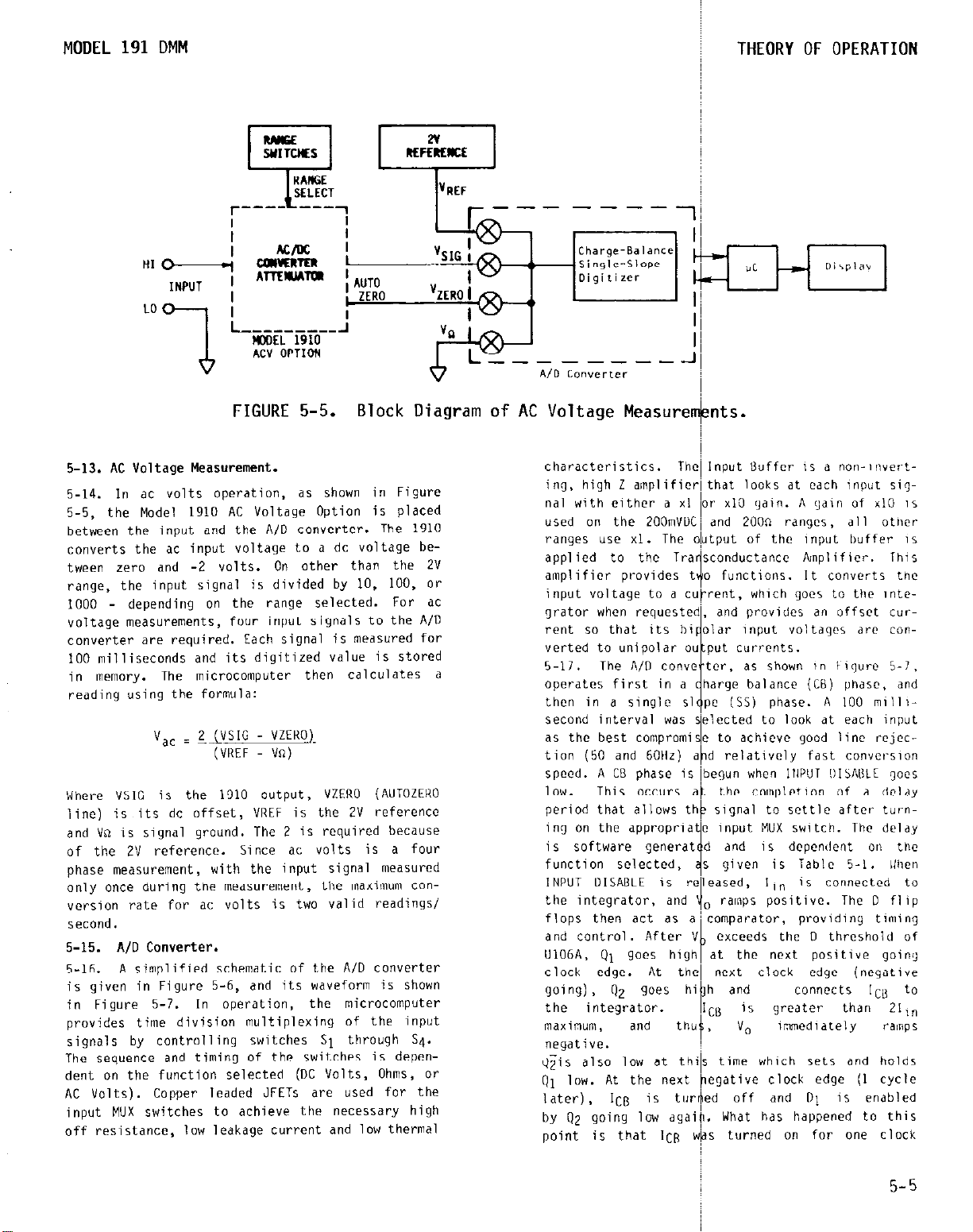
FIGURE 5-5. Block Diagram of AC Voltage Measure+nts.
5-13. AC Voltage Measurement.
5-14.
5-5, the Model
between the input and the A/D converter. The
converts the ac input voltage to a dc voltage between zero and -2 volts. On other than the 2V
range, the input signal is divided by 10,
1000 - depending on the range selected. For ac
voltage measurements, four input signals to the A/D
converter are required. Each signal is measured for
Where VSIG is the
line) is its dc offset, VREF is the 2V reference
and Vn is signal ground. The 2 is required because
of the 2V reference.
phase measurement, with the input signal measured
only once during the measurement, the maximum con-
version rate for ac volts is two valid readings/
second.
5-15.
5-16.
is given in Figure 5-6, and its waveform is shown
in Figure 5-7. In operation, the microcomputer
provides time division multiplexing of the input
signals by controlling switches S1 through 54.
The sequence and timing of the switches is dependent on the function selected (DC Volts, Ohms, or
AC volts).
input MUX switches to achieve the necessary high
off resistance, low leakage current and low thermal
In ac volts operation, as shown in Figure
1910
AC Voltage Option is placed
1910
100, or
100 milliseconds and its digitized value is stored
,n memory.
reading using the formula:
The microcolnputer then calculates a
V,, = L?VSIG - VZEKO).
(VKEF
1910
A/D Converter.
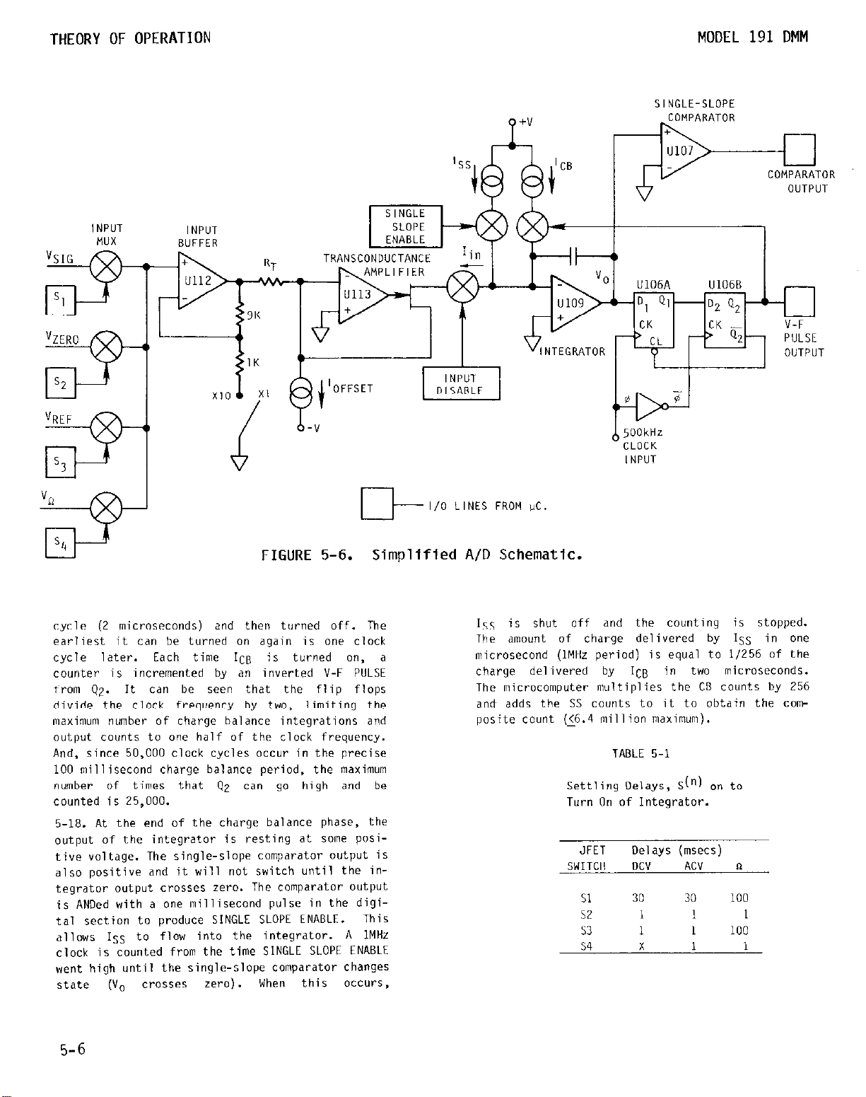
A simplified schematic of the A/D converter
Copper leaded JFETs are used for the
vn)
output, VZERO (AUTOZEKO
Since ac volts is d four
characteristics.
ing, high Z alnplificrlthat looks dt each input siqnal with either a xi or. x10 gain. A gain of xi0 IS
used on the 200mVDC~ and 2000 ranges, all otner
ranges
applied to the Tra sconductance Ainpiifier. lhis
amplifier provides t o
input voltage to d cufrent, which goes to the antegrater when requested, and provides a" offset CUTrent so that its hi alar
verted to unipolar ou
5-17.
operates first in a
then in a single sl pc
second interval was selected to look dt each input
as the best compramis,e to achieve good line rcjcction (50 and 60tlr) dbd relatively fast convex-soon
speed. A CB phase is ibegun when INPUT !II>AKLC goes
1OW.
period that allows thb signal to settle after tur-nlng on the appropriate input MUX switch. The delay
is software generat d and is dcpendcnt on the
function selected,
INPUT DISABLE is released, Iin IS connected to
the integrator, and
flops then act as a!comparator, providing timing
and control. After V
U106A. 91 goes high at the next positive going
clock edge.
wing)
the ikt$raraPd)rqs "'bb ""fs gre~~~:cct:ha/C"21:~
maXlGl""\,
negative.
d$is also low at
(h low. At the next pegative clock edge
I ater) ,
by 42 going low agaio. What has happened to this
point is that lC8 wbs turned on for one clock
“SE xl.
The A/II conve ter, as shown in iigurc 5-I.
This occurs al the completion of d dcldy
and th"
1~0 is turted off and D] is enabled
TheI input Uuffcr is a non-~nveit-
The output of the input buffer IS
functions. It converts the
1
input
voltdqes
put cur-rents.
barge balance (CU) phase. and
(8s) phase. A 100 mills-
/
5 given is Table 5-1. llben
,"
o ramps positive. The D flip
d
exceeds the " threshold of
At theI next clock edge (negative
P
13 v.
s time which sets and holds
thil
imediately rmp5
are con-
(1 cycle
5-5
Page 24
THEORY OF OPERATION
MODEL 191 DMM
El--
l/O LINES FROM UC.
*
+v
~RATDR -
U106A
D,
CK
’ CL
50OkHZ
CLOCK
INPUT
QI
U106B
-02 Q2 CK -
QZ--
r’-
cl
1
V-F
&iSE
OUTPUT
SINGLE-SLOPE
FIGURE 5-6.
cycle (2 microseconds) and then turned off. The
earliest it can be turned on again is one clock
cycle later.
counter is incremented by an inverted V-F PULSE
from 92. It cdn be seen that the flip flops
divide the clock frequency by two, limiting the
maximum number of charge balance integrations and
output co"nts to one half of the clock frequency.
And, since 50,000 clock cycles occur in the precise
100
millisecond charge balance period, the maximum
number of times that (12 can go high and be
counted is 25,000.
5-18. At the end of the charge balance phase, the
output of the integrator is resting at some posi-
tive voltage. The single-slope comparator output is
also positive and it will not switch until the integrator output crosses zero. The comparator output
is ANDed with a one millisecond pulse in the digital section to produce SINGLE SLOPE ENABLE.
allows ISS to flaw into the integrator. A 1MHz
clock is counted from the time SINGLE SLOPE ENABLE
went high until the single-slope comparator changes
state (vo crosses zero). When this occurs,
Each time 1,"~ is turned on, a
Simplified A/D Schematic.
This
ISS is shut off and the counting is stopped.
The amount of charge delivered by ISS in one
microsecond (IMHz period) is equal to I/256 of the
charge delivered by ICB in two microseconds.
The microcomputer multiplies the CL3 counts by 256
and adds the SS counts. to it to obtain the corn-
posite count ((6.4 million maximum).
TABLE 5-I
Settling Delays, SC") on to
Turn On Of Integrator.
JFET Delays (msecs)
SWITCH DC"
81
30
52 1
53 1
s4 x
AC" n
30 100
1 1
1 100
1 1
5-6
Page 25

MODEL 191 DMM
-+1.5v
THEORY OF OPERATION
P
CHARGE BALANCE PHASE
IOOmsec
ELA:
*FOR
5-19.
5-20.
control and display circuitry is given in Figure
5-8. This diagram also shows location of the circuits by printed circuit board.
5-21. Microcomputer.
5-22.
circuitry provide timing and control of both the
display and the A/O converter. Additional functions
provided by the microcomputer include the NULL
function and digital filtering. The Null function
is described in Paragraph 2-15 and digital
filtering is described later in this section. Count
prescaling, and recovery Crow d transient or‘ lost
program are additional functions provided by the
logic circuitry.
5-23.
system, that is comprised of d 6802 microprocessor
DIGITAL CONTROL and DISPLAY CIRCUITS.
A functional block diagram of the digital
The microcomputer and its associated logic
The microcomputer is d MicroBus 8 based
READOUT OF UP PRE-SCALE COUNTER
FIGURE 5-7. 191 A/D Waveform.
*
c
I
I
SINGLE SLOPE
PHASE __L
I msec
-B
ELA'
INTEGRATOR INPUT l
DISABLED -
N302) I
U303), and 1024 x R b&es of read only mm~ory which
provides the control ;program dnd is contnined on
either U305 (ROM) 0,. U304 and "305 (PROMs). The
microprocessor contdil/S a set of 72 variable length
instructions,
llWlll0ry (RAM) for tem+OTdTy storage. The FiA coo-
tdins four bytes 01 memory and provides the
Input/Output (I/O) c ntrol
the Imicrocomputer to
The microcomputer u+s partial memory decoding.
When Al5 is a logic I'O", either the 128 bytes of
RAM or bytes 129 thro gh
ted.
logic "0" RAM. logic !'I" PIA). When A15 is d logic
“1”
(ROM/PROMS),
512
A9 is high, the upper!512 bytes are selected.
d 6821 peripyerdl interfdce dddptw (Pin,
and 1281 x 8 bytes of rdndon, access
he other circuits in the ill.
1
A7 then determi es which is selected (A7 =
(high), read ~only rmemory is selected
and Ag Vetermines whether th? lower
bytes or the upper 512 bytes di-e selected. When
i:
*MEASUREMENT--c
lines for intcrfaclng
132 in the PlA dw selec-
NEXT
PHASE
@Registered Trademark of Motorola, Inc
5-7
Page 26

L --------- --__---__----
------ --1L ---------- 1
’ 3
g
F
FIGURE 5-8. Functional Block Diagram of Digital Control and Display Circuit.
5
Page 27

MODEL
191
DMM
2.5kHz
CHARGE BALANCE
START/m
CLEAR
COUNTER
THEORY OF OPERATION
FIGURE 5-9.
5-24.
5-25.
5-0, a logic "0" on PA7 indicates that the NULL
function is selected and a logic "1" on PB7
indicates that the instrument is in DC volts. These
signals are from the front panel NULL and WV pushbuttons, respectively. If not in DC volts mode, the
processor determines whether AC volts or Ohms has
been selected by looking at the value of the
reference voltage after it has been digitized.
5-26. Refer to Figure 5-8 and the timing diagram in
Figure 5-9 for
Charge-Balance phase begins with the MASTER RESET
line pulsing low, clearing U309A and 8 flip flops.
As described in the A/D converter discussion, the
appropriate signal to its input amplifiers is then
enabled by Sl,
After the completion of the appropriate delay
period given in Table 5-1, the "D" input to U309A
is made a "1". This same signal is ANDed at this
time to clear the H-F PRescaling counter U307. The
next rising edge of the 2.5kHz clock sets the Q
A/D Converter Control.
Looking at the A/D Controls Lines on Figure
the fallowing discussion. A
S2, S3 or S4 going to a logic "1".
Charge Balance Timing.
output of U309A low, ~enabling the input signal to
the integrator of thelAID. The processor now counts
250 interrupts from the 25kHz clock, and then sets
the "D" input to U309A to d "0". The next rising
edge of the clock sets INPUT DISABLE high again,
disabling the input 40 the integrator, and ending
the exact 100 millise ond integration period.
5-27.
PULSES are fed into lcounter U307. Each time the
counter overflows (a ter 256 counts) an interrupt
is generated which bhe processor counts in an
internal register.
the 8 most significant bits of the result.
5-28. At the end ofi the charge-balance phase, 8
bits of data are left on counter U307. This data is
obtained by pulsing t e MASTER RESET line into the
counter, and waiting
The number left on
minus the the
data becomes the ml die
result.
5-29. At the completi$n of remainder counting, the
Single-Slope phase ij begun by the SINGLE SLOPE
During the integration period above, V-F
1
1
Tfese interrupt counts become
1
for the counter to overflow.
he counter is equal to 256
1
number 'of MASTER RESET pulses. This
8 bits of the 24 bit
.j
5-9
Page 28

THEORY OF OPERATION
MODEL
191
DMM
FIGURE 5-10.
START/STOP signal going high, setting the "D" input
of U3098 to a "1". On the next rising edge of the
IMHr clock, the SINGLE SLOPE BEGIN signal from Q of
U3095 goes high, and is ANDed with the COMPARATOR
OUTPUT signal to enable single-slope counting. The
IMtir clock is now fed to U307, and counted similar
to the charge balance phase.
phase ends when COMPARATOR OUTPUT goes low, and
gates off the IMHr clock to the counter. The
remainder left in the counter is again read, as in
the charge-balance phase. This result is added to
the charge-balance counts to generate the 24 bit
(22 bit maximum) result. Timing for the single-
slope phase is shown in Figure 5-10.
5-30.
5-31.
5-8, consist of the LEO digits, and the necex~ary
decoding and driver circuits. These operate under
the control of the microcomputer. The diagram shows
the possible location of the decimal points, but
they are controlled by the range switching which is
not shown.
5-32. Display information is fed out on lines PAg
through PA6 of the PIA I/O bus. It is updated at a
2.5ktlr rate. with each digit an for approximately
400 microseconds. Since the display is fully aulti-
plexed, 6 updates are required to turn each of the
six digits of the display on once. This means that
the entire display is updated 416 times a second.
An update begins by blanking the display and disab-
Display.
The display circuits, as shown in Figure
The single-slope
Single Slope Timing.
eLAwy
FIGURE 5-11.
k
I
?""ZC
I
IN Ill":
Display Timing.
5-10
Page 29

MODEL 191 OMM
THEORY OF OPERATION
1
9.76 -102mscc pfriod U308
FIGURE 5-12.
ling the latch of "202.
PA6 pulsing to a logic "0" for 20 microseconds, and
the latch is disabled by pulsinq PA4 and PA5 to a
"1" for 10 imicroseconds. New segment data is now
presented on lines PA@ through PA3, and this data
is latched into U202 when PA4 and PA5 return low
after the
of the 20 microsecond period, the display is
unblanked, while new digit information is on the
PIA bus.
latched segment data being turned on until the
beginning of the next update.
shown in Figure S-11.
5-33.
5-34.
shown below the PIA on Figure 5-8. it consists of
two NAND gates, an AN0 gate, a 68OOpF capacitor and
counter U308 which divides by 256. Its function is
to restart the system by resetting the Microproces-
sor and PlA whenever either the prograiri is lost or
d long duration transient "CCII~S.
5-35. Timing of this circuit is shown in Figure
5-12.
10
microsecond period. At the completion
This results in the correct digit for the
Reset and Transient Recovery Circuit.
The reset and transient recovery circuit is
The circuit has two input signals, the 2.5kIlr
The display is blanked by
Reset and Transient Recovery Circuit Tilming.
Oisplay timinq is
i
1
I
k
l(i2nsec
clock and ILATCH ENARLi
by
U308 and LATCII ENA LE
normal operation, LAT$H iNARLt pulses low for 10
nicroseconds every 40
as described in the Di
Cb!ARLL is low, the vqltage on the cd~acitof (Vc)
rises exponentially. 1 When LATCI, LNARLC wt!irns
high, and while Vc is; dhovc the thwshold of thtz
ANn gate, a clear lpul e
normally U308 accuwul~tes one count and is then
cleared. A transient icdn mask the LATCH INAIII.C
pulses or a lost prag 'an, cd" prevent their appesrdnce at all. If no
128
seconds,
accumulate in U3fl8 afld its output will go high.
This high is NANOed {vith +5 volts to clear the
nlicroprocessor and Pld. Coincidently, LATCH FNABLI:
is forced low and Vc
U308
continues to cou t
it overflows after Z$snts, its ""put returns
low. This removes the!RESET and allows the micropr"cess"i- to return t the proper location in the
control
pr"CeSS.
counts r,",, the 2.5kHz clock wi,,
pr"gra"l. completes the recovery
The 2.5kilz clock is counted
is used to clear 11308. In
16
microseconds (2.5kKz r&e),
play discussion. k!hilr i~ATCli
%
1s applied to "308. Thus.
{
ulses appear for 5, milli-
a
b 1 gins to rise to its naxiriw.
the 2.5kHr clock dnd when
5-11
Page 30

THEORY OF OPERATION
MODEL 191 OMM
1 FIUXFET
INPUT BUFFER
FIGURE 5-13.
5-36. Digital Filtering.
5-37. When the 200mV or 200 Ohm range is selected,
a logic "0" is applied to PB7 of the PIA, which
tells the microprocessor to filter by averaging the
last 8 readings. For this condition, the last 8
readings are averaged together and displayed, as
lonq as the latest conversion is within digits of
the prfvious diplay. If the new conversion is more
than + digits away from the previous wading, the
new reading is displayed. Thus, speed is attained
for large signal changes, but random noise is reduced by a factor of 8. For all other ranqes, the
microprocessor USES a threshold of +5 digits and
averaqes the last 4 readings. Thus, snallcr siqnal
changes arc responded to, while random noise is
reduced by a factor of 4.
5-38.
5-39.
fom in the lower riqht corner of Figure 5-8, and
the complete circuits are shown on page 2 Of
Schematic 301620. Basically, the 4MHz crystal
control oscillator is a Pierce type oscillator. Its
4MHr output is fed direct to the clock divider
before application to the microprocessor (U302).
11105 provides three outputs by dividing 4MHz by 4,
8 and 16.
inverters to provide zero to t4 volt square waves.
The 1MHz output is used for Single-Slope countinq,
5OOkllr is
Charge-Balance timing, and 25Oktlr is divided by 100
in U301 to produce the 2.5kHz clock.
Oscillator and Clock Divider.
These circuits are shown in block diaqranl
(U105),
and it is buffered by a CMOS inserter
Its outputs arc buffered by CMOS
used in
the A/D converter for
9k
Turning on JFET Switches.
5-40. A/D CONVERTER CIRCUITS
5-41. The A/D convfrtfr rust have a high input
impedance and be linear to within a few parts per
million over the + 2 volt operating range. To [meet
this critera, several innovative circuits had to bc
desiqned. These circuits are described in the
following paragraphs.
5-42. Input Buffer.
5-43. The input buffer is a non-inverting. hiqh
input impedance amplifier which looks at each input
with either x10 or xl lain. Its input signals are
multiplexed by switches Sl through 54 under the
control of the microcomputer. One of the first
problems encountered was the high transients that
appear as the multiplexing switches are turned on.
The effects of these transients were eliminated by
the use of software generated delays.
EYCP, necessary to drive the gate of the appropri-
ate JFET with the input siqnal voltage to turn 1t
on. This was accomplished with a bootstrap ampli-
fier (BSA) connected to the invertinq terminal of
the input buffer (SEE Figure 5-13). When switch 5
is opened, the gate of Q rises to the output of BSA
which
t"mS q on, which means that VI,, = V) = VG.
Note that this technique works regardless of input
buffer gain.
equals the
0
lk
It was, how-
input voltage (V[N). This
5-12
Page 31

MODEL 191 DMM
THEORY OF OPERATION
FIGURE 5-14. Power Supply Comon Bootstrapped to Input Voltage.
5-44. As previously mentioned, the A/D convcrtfr
was designed for linearity. This means that the
input buffer must be linear over the full ~mfasurement range of t2V to no more than a few parts per
million. Since it also must be non-inverting, with
very hiqh input impedance, its gain linearity would
normally be determined by common mode non-linearity.
Most amplifiers specify 80 dB CMKK, and since CM
non-linearity would typically be a factor of 10 or
better, one could expect 10 ppn non-linearity frolv
CM Effects.
error, it was required that the common mode ~frors
be reduced.
either by improving CMRK through critical sclcction
of devices, br by eliminating the colirnon mode (CM)
voltage. The latter method was chosen, as shown in
Figure 5-14.
inverting operational amplifiers, the common mode
voltage
(power supply common). Thus, it can be seen that if
"IN -
common mode errors would be zero because VCM =
0. To achieve this,
Since this would be far to" much
Common mode errors can bf "v~rcomf
First consider that, for non-
(VCM) is equal to VIN VCOM
VC-M could
be made equal to Zero,
it was necessary to bootstrap
the power supply con~ion for the input a,n,i,if~cr- i)t
the input voltage. This wds accomplished !)y d:ld)":;
2 zmers, 2 transistbrs, and d few resistors. :hr
power supply common :is seen to be thr junctlori of
VKIOS and VI1106 (the ;"utPut of INSA), which is eqiial
to
"IN.
0, and the common mbde error is elininatcd. !i"te
that this techniques also raises input inpcdancc
because:
And, since there is in" bias change on the input
FETs of the input1 amplifier,
Z[NW". With the &mm"n mode error elimnatcd,
the only gain error is "pen loop gain nonlinearity
divided by loop gainj For closed loop unity ~jain,
non-linearity is 0.5 :ppm since "pen loop gain non-
linearity is 10% and "pen loop gain is 200,000.
For x10 gain, nonlinebrity is 5 PF~I.
Thus. VC,, =
VIII
I,!{= J and
"UX.!;F
5-13
Page 32

THEORY OF OPERATION
IO = Ioff - Iin
MODEL
OUTPUT
191
DMM
Ioff
is made + Vin
Rin
Thus \,hen Vi" = Vin max, 10-0 (pcs. full scale)
Vin =O, IO 'Ioff (zero)
Vin = -Vjn max.
FIGURE 5-15.
5-45. Transconductance Amplifier.
5-46. This alnplifier performs two functions. It
converts the input voltage to an output current
that is sent to the integrator on request. It also
provides an offset current so that its bipolar
input voltages are converted to unipolar output
C"!-"?CTltS. BEcause of
operation, its linearity is cxccllent. Figure 5-15
shows how the circuit operates.
5-47. Integrator.
5-48. The integrator has been dfsigned to guard
against the !m"st common problems associated with
high speed integrator operation.
tors have two Imajor problems which limit their high
speed performance. One is the GAINBANDWIDTH of the
integrator amplifier, and the "th"r is the output
resistance of the same amplifier.
the current mode of
Io= Ioff + Vin max*z Ioff (minus f-s.)
Transconductance Amplifier Operation.
Active integra-
These effects
Flax.
Rin
can be seen by looking at the integrator rmodcl in
Figure 5-16. If a voltage step appears at Vi".
the amplifier will not respond immediately, and C
will initially be a short circuit. As shown in the
equation, the effect is that the wrong current will
be applied to the capacitor until the amplifier I‘"covc~s. It can also be seen that if a bipolar input
amplifier was used for the integrator, charge could
be conducted away from the capacitor and cause
significant ~rr"rs. To guard against these problems, the 191 uses an emitter follower on the integrator output to keep I?" small into the MHz region, and ail inputs to the integrator are current
sources. Also, FET input operational amplifier is
used, which would allow a few volts to appear on
the summing junction with no loss in charge.
5-14
Page 33

MODEL 191 DMM
THEORY OF OPERATION
For step voltage inputs:
FIGURE 5-16.
REFERENCE
DIVIDER
+2v
+.2v
Integrator Problems at High Speed,
e-e0 = Vin
2.74k
+
6.1
13
k
k
FIGURE 5-17.
6
Simplified Schematic of Reference
UPPlY.
5-15
Page 34

rHEORY OF OPERATION
MODEL
191
DMM
5-49.
5-50.
5-17.
was designed for linearity and low noise. This
means that stability and accuracy must be provided
by the reference.
cuit is a buried layer zener diode, with an "n-
board heater, which was selected because of its
stability, low noise,
and low dynamic resistance. It is driven by a con-
stant current (nominally ImA) developed by amplifier U102. Since the zener current is well regulated,
Far example: a 1 volt change In +V would only cause
a zener current change of about 150 nanoamperes.
And, since the dynamic resistance of the zfner is
0.5 ohms, the zen~r voltage would only change 7.5
nanovolts. Super stable tracking resistors are used
in the reference divider to provide very stable 2
volt and 0.2 volt reference voltages. The input
resistors of the divider are specially selected
nominal 100 microamperes of current to the divider.
For example: the values of resistance shown in the
diagram would be for a zener voltage of 6.95 volts.
5-51.
5-52.
tage regulators,
switching and full-wave rectifiers which make up
the power supply for the Model 191. There are three
component regulator used. The plus and minus 15
ment.
+ 5% dCC"raCy. Its input voltage is supplied from
REFERENCE SUPPLY.
The reference supply is shown in Figure
As previously mentioned, the A/D converter
The heart of the reference cir-
low temperature coefficient
it is imune to power supply variations.
(depending on the zener voltage) to provide a
POWER SUPPLY.
Page 4 of Schematic 301620 contains the vol-
line transformer, line voltage
integrated circuit
volts dc is provided by VRlOl and VR102, respectively. These are 3-terminal regulators with + 10%
accuracy.
volts dc from TlOl and
selected line voltage is supplied to the instru-
and input currents are limited by RI58 and R159.
Output voltages are filtered by
VR104 provides the t5 volts used in the analog
(ANLG) circuitry. It is a 3-terminal regulator with
TlOl and CRIOI,
(+0.5V) with minimum selected line voltage applied.
Input filtering is provided by
filtering by C116. 9126 and Q127 comprise a series
regulator which provides +5 volts for the Digital
and Display circuitry.
thus,
approximately 6.5 volts (+0.5V) from TlOl and CR103
when minmum selected line voltage is applied. Input
filtering is provided by C109, and CR106 prevents
thermal runaway in the event of a circuit fault.
They receive approximately +I8 and -18
lnput voltages are filtered by
has the same output accuracy.
regulators and one discrete
CR102
and is approximately 8 volts
It is slaved to VR104, and
when the minimum
Cl11
and Cl14
Cl10
and C113.
C115,
and output
It recei vcs
The allowable zener voltage is between 6.6 and 7.3
volts, with the resistors matched accordingly.
MODEL
1910
5-53.
5-54. The Model 1910 is basically a plug-in acldc
converter with variable gain that conditions the ac
input voltage for application to the A/D c""wrtfr.
The basic transfer function of the acldc converter
is shown on the simplified schematic (Figure 5-18).
The resistor values were selected so that
rn*~N = -I
ages above 2 volts, the feedback resistance
(Rf) is
range) to keep the output always less than -2Vdc.
The dc output is a half-wave rectified sine wave,
and the converter is average responding, calibrated
to the rms value of d sine wave.
blocks dc inputs, and the dc offset voltage of the
amplifier is autozeroed out. Output filtering is
provided by the combination of resistors K404-K406
and capacitors C401-C405.
5-55. In actual circuit operation (as shown in
schematic 299600, Section 7) the feedback rcsistante of U401 is controlled by K401, K402 and K403.
llith all three relays de-energized as shown, the
overall gain of the acldc convcrtcr is unity (i.e.,
1 Vat rmsIN = -1 VdcOUT). ilith both
K401 and K402 energized, gain is t
10 when K403 is energized with K401 and K402 deenergized. The relays are controlled by the front
panel range pushbuttons via the range select lines,
as shown on sheet I of schematic 301620. See Table
5.2 for gain chart of the ac voltage ranges.
*See Figure 5-18.
reduced (by selection of d higher
Attenuation
AC VOLTAGE OPTION.
‘%IuT.
Table 5-2
Gain Chart for AC Voltage
U401 FDBK
Resistance (Rf)*
For ac Input VOl t-
-__
499 kn
49.7 kn
4.7 kn
250.2 n
Capacitor C415
1000.
Energized
Relays
-
1
i
1
Gain is
NOW
K403
K402
K402.401
Vat
?
5-16
Page 35

MODEL 191 DMM
THEORY OF OPERATION
'499kri
Basic Transfer Function:
*See Table 5-2 for feedback resistance CRf) vwsus range.
FIGURE 5-18.
Simplified Schematic of Model 1911
-L
c401
J i
OAUTO ZERO
-L
c405
5-17
Page 36

Page 37

MODEL 191 DMM
SECTION 6. MAINTENANCE
6,-l.
GENERAL
6-2. This section contains information necessary
to maintain the Model 191 DMM and the Model 1910
AC Volts Option. Adllstmentlcalibration, troubleshooting, and fuse replacement procedures are
provided. Calibration should be performed yearly
(every 12 months) 01‘ whenever performance verification (see Section 3) indicates that the Model
191 is out of specifications. If any step in the
calibration procedure cannot be performed properly, refer to troubleshooting information in
this section OP contact your Keithley representative or the factory.
NOTE
Calibration should be performed by qualified personnel using accurate and reliable
equipent
6-3. RECOMMENDED TEST EQUIPMENT.
6-4. Recommended test equipent for calibration
is listed in Table 6-l.
may be used. However, the accuracy of the alter-
nate test equipment must be at least 3 times
better than the Model 191 specifications, OP
equal to Table 6-1 specifications.
6-5.
ENVIRONMENTAL CONDITIONS.
6-6.
Calibration should be performed under
Alternate test equipment
MAINTENANCE
laboratory conditidns having en ambient tcmperature of 23 +l"C, abd d relative humidity of less
than 70X. If the ihstrument has been subjected to
temperatures outsidp of this range, or to hlgherhumidity, allow oneihour minimum for the instrunent
to stabilize et the specified environmental
conditions
procedure.
6-7.
6-8.
the adjustments indicated to calibr.ate the Mode!
191 DMM.
6-9.
6-10.
Model
access to the Model1
ing the instrument to reach normal internal operating temperature.
follows:
before beginning
cALmffAT10~
Perform the ifollowing procedures dnd make
Installation bf the Model 1913 calibration
cover.
Calibration Ishould be performed using the
1913
calibratbon COVET. This cover permits
Disconnect!the line cord before rci!ioving
the cover.: To discharge voltage on
capacitors, depress the OFF/ON pushbutton after
cord.
PROCEDURE.
191
Install
t,
WARNING
adjustments, while allow-
disconnecting
the
calibration
the COYCI 3s
the
ii"?
Item Description
DC Calibrator
AC Calibrator
High Voltage Amplifier
(Used with Model 74511)
Decade Resistor
Kelvin-Varley Voltage
Divider(Used with Model
343A)
Recommended Test Lquipnent For Calibration.
TABLE 6-1.
Soecification
19v,19ov, 1ooov
?0.002% or 2ouv
O.lV, IV, IOV, IOOV
*o.o2z
1000 v
to.049,
1900, 1.9Kn 190Kn
Certified to 50 ppn
.19v, 1.9v
ilith 2 ppll
Terminal Linearity
Plfr. : Model
Fluki
K-P ~,
H-P
343A
745’“s
746A
ESI ~ RS725
Fluke
72OA
6-1
Page 38

MAINTENANCE
MODEL
191
DMM
Turn off power and disconnect the line cord.
d.
Turn the instrument over so that the bottom
!L.
cover is facing up, loosen the four screws in the
bottom panel.
rubber O-rings.
Hold the top and bottom covers together to
C.
prevent their separation and turn the DMM "vcr to
normal position.
1. Carefully lift off the top cover.
e. Position the calibration cover in place on the
Model 191 and tighten the bottom panel screws.
6-11. warm up.
6-12.
pushbutton to ON position. Allow a one hour warm-up
time before beginning the calibration adjustments.
6-13.
6-14.
6.15. The troubleshooting instructions contained in
this section arc intended for qualified personnel
having a basic understanding of analog and digital
electronic principles and components used I" a orecision electronic test instrument.
have been written to assist in isolating the defectiye circuit or subcircuit. Isolation of the specific defective component has been left to the technician.
Connect the line cord and depress
Calibration Adjustments.
Some procedures require the USC of high vnltaije.
Take care to prevent contact with live circuits which could cause electrical shock re-
sulting in injury or death. Use an insulated
tool when making adjustments.
a. Refer to Table 6-2 and perform the listed ad-
justments in the sequence indicated.
the step sequence is also indicated on the Model
1913 Calibration cover by box numerals.
sequence must be followed exactly because the adjustments are interrelated and dependent on the
preceeding steps.
calibrate the basic Model 191. If the Model 1910
AC Volts Option is installed, also perform steps 9
through 15.
Following calibration, to insure that all
5.
functions and ranges are operating properly, iuti-
lire the Performance Verification procedure in
Section 3.
If calibration cannot he accomplished or the
C.
Performance Verification procedure indicates a
problem, proceed to Troubleshooting information in
this section.
TROUBLESHOOTING.
These screws are held captive by
OFF/ON
\ WARNING
Note that
The
Perform steps 1 through 8 to
Instructions
NOTE
For instrunents that are still under warranty
(less than 12 months since date of shiomenti.
Tf the instrument's performance is outside of
specifications at any point,
Yeithley representative or the factory before
attempting troubleshooting or repair, other
than fuse replacement.
6-16.
6.17. This section contains tables listing step-by
step checks of the major DMM circuits descibed in
Section 5, Theory of Orteration. The following steps
outline the use of these tables and provide instrrrction for preparing the DMM for toubleshooting. liead
all of these steps carefully before troubleshooting
the instrument.
6.18. it may be necessary to remove the shields on
the mother hoard and the Model 1910 AC voltage
Option (if installed) to gain access to test points
and circuit components for troubleshooting.
6-19.
G-20. Perform the following procedures to remove/
replace shields an molher Lboard and Model 1910 AC
Voltage Option.
TROUBLESHOOTING PROCEDURE.
NOTE
Recalibration of the Model 1910 AC Voltage
Option ~may be necessary if any of the follow-
ing occurs.
1) ilerr~oval/Re,~lacen~ent of Model 1910.
2) Disturbing position of Model 1910 in the
C"""eCt"r.
3) Iler~~"val/Keplace~~lent of shields on the Model
1'110.
Refer to Section 3-13
accuracy. If calibration is necessary perform
steps 9 through 15 in Table 6-2
Shield Removal/Replacement.
t
Disconnect the line cord before removing ttie
case COYPT.
2. Turn off power and disconnect the line cord.
Remove four SC,-ews fro," the botton, of the case and
separate the top cover fro", the botton cover.
b. Remove smother board shield by carefully lifting
shield from the retaining clips. To reinstall,
position shield on the four retaining clips so
that the small bent tah on side of shield is
positioned against the grounded retaining clip
(See Figure 6-Z).
from moving to" far towards the rear of the mother
board.
fully into retaining clips.
IPress firnlly on top of shield to engage
This tab prevents the shield
to
WARNING
contact your
check AC Voltaqe
6-2
Page 39

MODEL 191 DMM
MAINTENANCE
t 1.0
DC
Calibrator
(A)
OUT
LOW
I
SET TO
1o.oooooov
FIGURE 6-1. Test Circuit For 200nVDC And 2VDC Calibrhtion.
c. To gain access to shields on the Model 1910 AC
Voltage Option disconnect the brown and blue wires
at the pushbutton switch and completely remove the
Model 1910 from connector P1006.
from PC board by removing the two retaining screws.
Refrain from any unnecessary touching of circuit
components.
verse the procedure to reinstall the Model 1910.
The wiring instructions for the Model 1910 are
located on the mother board shield.
6-21. Special Handling of Static Sensitive
b-22.
high impedance levels for low power consumption.
For this reason, a normal static charge build up on
your person or clothing can be sufficient to destroy
these devices.
sensitive devices in your Model 191 and provide
instruction on how to avoid damaging them when they
must be removed/replaced.
CMOS devices are designed to function at very
a. Static sensitive devices:
Keithley
Part Number Designation
LSI-8
LSI-18 u302
IC-168
The above integrated circuits should be
LT.
handled and transported only in protective containers.
tubes or static protective foam. Keep the devices
in their original containers until ready for use.
Handle the board by its edges.
Devices.
The following steps list the static
Reference
u303
u202
Typically they will be received in metal
Detach shields
.0190000 FOR CAL
STEP 4b.
.1900000
b-
SET TO
FOR CAL
STEP 5.
MODEL
191
4-l
Remove the devicies frolv their protective con-
C.
tainers only at d pr/operly gounded war-k bench 01
table, and only afteb grounding yourself by using
d wrist strap. ~
Handle the devic~es only by the body. 00 not
d.
touch the pins.
e. Any printed circlit board into which d device
is to be inserted mvst also be grounded to th?
bench or table. ~
f. Use only anti-stt+tic type solder suckers.
9. Use only grounded tip soldering irons.
h. After soldering ,he device into the boat-cl,
or properly inserting it IntO the
receptacle, the deviqe is adequately protected and
normal handling can tje resumed.
6-23. Line Power. ~
6-24.
6-3, Line Power Checqs to verify that the pow?!
supplies are providing the correct voltages to the
electronic components.i
6-25.
G-26.
display should bc vctified bcforc troubleshooting
the signal conditionipg circuits.
convertor and displab per Tables 6-4
respcctivcly.
6-27.
G-28.
Model 1910 AC VoltdgCi Option.
per Table G-6.
In genera,, *tap tra"bleshooti"q with Table
A/D Converter a'jld Display.
proper operation of ttlc n/o convcrtcr dllil
Cheek tnc AllI
AC Converter.
Problcns +lith\ ac voltage !aay involve the
Check this c,rcuit
Inat i nq
and G-5
6-3
,
Page 40

MAINTENANCE
MODEL 191 DMM
TABLE 6-2.
Calibration Adjustments.
step Function
ia n ZOOQ Dial "0" Ohms,
lb II 200n
2a n
2b n 2Kn
3
4a
4b
5
6
7 UC v
8 IN v
9
n 2OOKn
DC v 200 rn"
DC " 200 a"
IOC v 2 v Release NULI., 1.9OO"O ice !iqure h-i
UC "
AC v
Range
2Kn Dial "0" Ohms,
Applied* Adjustment Desired Test
Input
depress NULL 00.000 Decade IResistor (0
190
reset NULL .ooooo Decade Resistor
1.9Kn K123 1.90000 Decade Resistor
Release NULL.
19OKn I(124
Disconnect DC
Calibrator,
Short Input
depress NULL
.+190 I”” Ill25
t1.9 v 1126
2"" "
20 v
1000 Y +1000 v
1000 v
1190 v
+19v
IOOOV at Ik Hz i1401 1000.00 AC Calibrator (IS)
Point** Reading Equipment
Kl22 190.000
190.000
""."O" See Figure 6-I
190.000 See Figure 6-l
I1132 190.000 OC Calibrator (A)
11131
11130
19.0000
1000.00
Decade Resistor
Decade Resistor
IIC Calibrator
1)C Calibrator
and IHigh Voltage
Amplifier (C)
10
11 AC v
12
13
14
15
* Connect to INPUT ill and LO terminals.
l
* Refer To Figures 6-2 and 6.3 for location of Ad.iustment Points.
AC v 2v
20 v 1OV at lk Hz
AC V 200 v
AC V 200 v 1OOV at 5OkHz C412 100.000
AC V 2V
AC V 20 v
calibration.
IV at
Ik Hz 11410
11411
1OOV at lk Hz
1V at 50 ktlr
1OV at 5OkHr c4ox 10.0000 AC Calibrator
K409
c411 1 .ooooo
SENSE terminals should not be used during
1 .ooooo
10.0000
100.000 AC Calibrator
AC Calibrator
AC Calibrator
AC Calibrator
AC Calibrator
6-4
Page 41

MODEL
191
DMM
MAINTENANCE
LINE FUSE F 101
\
+5
-15
DIGITAL BOARD
+15
x122
R123
R124
R125
R126
GROUNDED RETAINING CLIP
FIGURE 6-2.
Model 191 (Shield Removed)
6-5
Page 42

MAINTENANCE
MODEL 191 DMM
- R401
R409
.R410
-R411
C408
6-6
FIGURE 6-3.
-c411
.c412
Model 1910 AC Voltage Option (Shields Removed)
Page 43

MODEL 191 DMM
MAINTENANCE
6-29. DC Attenuator and Ohms Source and Resistors.
6-30. Problems with dc voltage or resistance ranges
may involve these signal conditioning circuits.
Check these circuits per Tables 6-7 and 6-8.
NOTE
Dust, flux or other contamination will degrade
performance on resistance and dc voltage ranges.
6-31. Digital Board.
b-32. Problems may exist with the microprocessor or
associated circuitry.
6.33.
common (INPUT LO terminal), unless otherwise noted
in the tables.
All measurements are referenced t" analog
Check out per Table 6-9.
STEP ITEM/COMPONENT
1 S102 line Switch
2
FlOl line fuse
REQUIRED CONDITION
Must be set to 115" or 230V
as appropriate.**
Continuity
6.34.
possible blown fuse (line power) refer t" Paragraph
6-35 for fuse rcolacetncnt instructions.
TABLE 6-3.
Line Power Checks.
If a gross f4ilure exists that indicates d
j UARNING
Some procedures in the foilowing tdbie~
require the $e "f high voltage.
to prcvcnt c+~tact with llvc cIrcult% wli:ch
could cause $lectr,cal shock r-rruit!",; ,n
injury or dcaith.
at INPUT LO ,P"tcntial.
floatinq high enough will create d thick
hazard betwccln the shield dntl i!ar-tll gr'oiind.
The ,m"thcr boar-d ~hifir! :I
A" input vo!ta9c
@MARKS
rake care
3
PI014 line cord
4
5
t5V pad*, Analog
6
"R104, IN.
7
t5V pad*, Digital
8
Emitter of 4126
tl5V pad*
9
"RIO1 IN.
10
-15
I1
12
* On main printed circuit board (see Figure 6-Z).
**On optional line voltage units set to 115V.
pad*
VR102 IN.
Plugged into live receptacle
Turn on power
15 volts, +54,
t7.4 volts
minilwn
+5 volts, 25%
i-6 volts minimum
t15 volts,
i-17.9 volts minimum
-15
volts, '10%
-17.9 volts minimum
210%
Output Of vi1104
Coll~ector "f 0126
OutpIut Of VRl02
lnp"!t to "Rio2
NOTEi: Not regulator
inay Iindicate shorted
I Odd.
G-7
Page 44

MAINTENANCE
MODEL 191 DMM
TABLE 6-4.
A/D Converter.
CTFP I ITFM/C"MP"NFNT
,,_, .._..,_~...~.._~..
1
Display
2
UlD4,pin 10
3*
U104,pin 8
4*
Ul04,pi" 12
5*
U106,pin 3
6
7 U106,pin 11
K138
8
U113,pin 2
9
Ull4,pin 2
10
IKFIIIIIKED CONDITION
. . . . ~~~~
T",T 0" power. select 1000 VDC. NOTE: Some tests
000.00 12 Digits
0 to +4 volt square wave
at 4 MHz
0 to t4
at 1 MHZ.
volt square wave
I
0 to 14 Volt square WaYC
at 250
0 to 14
at
0 to t4
at 5OOkHr
0 volts for 400 milliseconds
-2.5 volts, ?7% ( 175mVolts)
ii volts, 17% ( 350mVolts)
ktiz
volt square WaYe
500
kHr.
volt square WaYe
t2 volts for IO0 milliseconds, Input Ruffer output
REMARKS
here could fail
because of Digital
Board problems and
YlCC Yersa.
4 MHz clock (P1005,
pin 2).
1 MHz Clock (P1005,
pi" 7).
250 kHz clock (P1005
pin 3).
500
kllz clock
500 kHr clock
Transconductance Pmp
bias.
Charge Dispenser
bias
Cl12
11
12 Cl12
13
External voltage
14
SO"t-Ce
Display
15
16
External Voltage
17
SO"I‘C!2
18
19
Display
External voltage
20
source
21
Display
LI
* Skip these‘steps, if steps 1 through 4 on Digital Board (Table 6-9) have been
performed.
0 volts +I5 millivolts
See waveform per Figure 5-7
Select 2 V DC Range
Apply +I.90000 volts
1.90000 *IO digits
Select 200mV OC range
Apply .OOOOOO volts
Depress NULL
00.000 *I digit
Apply
+190
millivolts Calibration point
190.000 210
digits
Integrator input
Integrator output
Calibrated point
If different, check
2 volt reference
(pin 7, 200mV
switch).
Calibrated point
Input offset nulled
If different, check
0.2
volt reference
(pi" 9, 200mV
switch) or X10 gain
Of Input Buffer.
6-8
Page 45

MODEL
191
DMM
MAINTENANCE
TABLE 6-5.
Display.
TEP 1 ITEM/COMPONENT
1
2 +5V Digital Pad* +5 Volts eJ%
or P1002, pin 4
3
U201, pin 1,2,6, Digit drive. Low-enabled
7.9 and 13
4
U202, pin 9,10, HI-enabled
11,12,13,14 and
15
5
U202, pin 4 and 5 Negative - going pulse (t5V
6
J1002,
and 8 high (on).
-
* On main printed circuit board. See Figure (6-Z.)
pins 2,5,7 Appropriate DP line
IREQUIRED CONDITION
Turn on power. Select 1000
v DC range.
to OV) occurring every 400 rec.
(2.5kHz).
REMj,RKS
I
If low,icheck per
Table 6+3.
LED cathode
7 %gme$t OUtpUtS
Oepress~RANGE
pushbuttons to
checkall W's,
6-9
Page 46

MAINTENANCE
TABLE 6-6.
AC Converter. (Model
MODEL 191 OMM
1910)
STEP
1
ITEM/COMPONENT
Display
Pin 1, DCV
Switch
Pin
12,
ACV
switch
External voltage
source
REQUIRED CONDITION
Short input
.OOOZO *lo digits
10 millivolts
Same as step 4, plus reading
at step 3.
Apply 1.00000 volts rms
at 1kHz
REMARKS
NOTE: Full scale
input on all ranges
should produce
approximately -2V
DC at output. (pin
I, DC VOLTS switch).
NOTE: Do not perform unless AID
tests are completed.
Normal ZWII offset
range.
Impedance meter to
measure
(1090).
Output resistance is
300
kn
ACV Auto zero.
Calibration point.
Display
Pin I, DCV
switch step 4
Pin 12, ACV Same as step 5
switch
10
11
External voltage Apply
souI‘ce
12
Display
13
External voltage Select 200 VAC range
SO"lW2 and apply 100.000 volts rms.
14
Display
1.00000
-1
NOTE: If any of above checks
fail, proceed to bias checks,
step 18.
Select 20 VAC range
at 1kHz
10.0000 SO0
100.000
+lOO digits
volt, plus reading at
10.0000
volts rms
digits
?I00 digits
DC OutpUt
Auto zero
Calibration point
Calibration point
6-10
Page 47

MODEL
191
DMM
TABLE 6-6. (Continued)
AC Converter. (Model
MAINTENANCE
1910)
STEPS
16
17
18 TURN OFF POWER.
19
20
21
ITEM/COMPONENT
15 Select 1000 VAC range
External voltage Apply 1000.00 volts rlns
SO"V2e
Display
Pin 2, U401
R405, CR401
R402, R406
REQU1KELl CONDITION REMARKS
1000.00
Remove Model
Voltage Option from Model
191.
install Model
191.
short INPUT. Turn on power.
0 volts +I0 millivolts. Sunning junction,
0 volts +lO millivolt5 DC output before
0 volts *IO millivolts Fcedhackicircuit
+lOO
digits
1910
Remove shields and TE-
1910
Select 2VAC range and play
Calibrat/on point
NOTE: w/th shields
AC removcd,~ display
will he noisy and
read man! millivolts
in Model
of AC pikkup. Ois-
wilh also
change wbth operator
inovelnenti
AC amplifier.
filter.
22
23
24
Q404, base
0403, emitter
Q401, base
-7.5 volts *IO%
t5.7 volts
-3.6 volts *lo%
NOTE: Model
calibrated if step
formed.
*10x
1910 must
be rf-
18 was
Base voltage
5 milliabp current
y3urce.
Rias foriC404
protectibn circuit.
per-
6-11
Page 48

MAINTENANCE
TABLE 6-7.
DC Attenuator.
MODEL
191
DMM
.EP
ITEM/COMPONENT
1
External voltage
2
3 Display
4
5 External voltage
source
6 Display
7
8 External voltage Apply
source
REQUIRED CONDITION
Turn on power. Select
2oov DC range.
Apply t190.000 volts
190.00 i10 digits
Select 2OV DC range
Apply
19.0000 *IO digits
Select 1000 VDC range
t19.0000
tlOOO.OO
volts
volts
REMARKS
NOTE: These checks
should not be made
if a problem exists
on the 200mV DC or
zvoc ranges.
Calibration point
1OO:l Attenuator
(R129A,R,C,D, RI24
wiper).
Calibration point.
IO:1
Attenuator
(R129A,B,C,D, R131
wiper).
Calibration point.
9 Display 1000.00 f5 digits
1OOO:l Attenuator
(R129A,B,C,D, R130
wiper).
6-12
Page 49

MODEL
191
DMM
MAINTENANCE
TABLE 6-8.
Ohms Source and Resistors.
;TEP ITEM/COMPONENT
1
2
Display
Pin 5, ACV
3
switch
4 Pin 3, U103
5
6 Display
1
Pin 5, ACV
8 Pin 3, U103
REQUIRED CONDITION
Select 200 range and short
INPUT with 18 gage (or lower
copper wire. (tin plated OK
Less than
-0.4 volts *9%
-0.4 volts
Select 2Kn range
.OOOOO +2 digits
-4 volts ?7%
-4 volts k7%
00.010
kl%
R[MARKS
NOTE: ~DO not perform uhless AID convertcwand DC
attenupor tests are
completed.
Two wipe offset, includinb thermals.
Ohms reference
WI taqp
Ohms rkference
divider.
Ohms rieference
vo1taqp.
Ohms r~fetcncc
divideir.
9
10
11
12
13
14
15
16
1.00000 k n
Display
Pin 5, ACV
INPUT ill
lO.OOOOk n
Display
lOO.OOOk"
resistor
Apply to input
(4-wire connection)
I.00000 ?I0 digits
-4 volt5 ?7%
-2 volts +7% (half of step 1
Apply to INPUT and select
20kn range
10.0000
IRepeat Steps
Apply to INPUT and
select 200kn range.
210
digits
11
and 12
Calibrated
reslstiance
Range iresistors :
R107,
iK109. I)105
QiO6 aire protection
trdnsilstor-5.
Ohms rjeference
Volta@.
Volta+? across unknown.;
Caliblated
rE515tpCe
Calibflatcd
resisqance
and
6-13
Page 50

MAINTENANCE
MODEL 191 DMM
TABLE 6.8 (Continued)
Ohm5 Source and Resistors.
STEP
17
18
19
20
21
22
23
ITEM/COMPONENT
Display
1
.OOOOM
0
I‘e515tor
Display
10.000
re515toT
Display
Mn
REQUIRED CONDITION
100.000 210 digits
Repeat Steps 11 and 12
Apply to INPUT and select
2000kn range.
1.00000
Repeat Step 18
Apply to INPUT and
select 20Mn range
10.0000
+30 digits
+lOO
digits
REMARKS
Range resistors:
R107, 11109, R129D.
K130,
R129C, R124.
Use meter with high
input impedance
(bO%).
Calibrated
resistance
Range resistors:
R107, R109, R129D,
R130,,
Rl29B,
Use meter with high
input impedance
R129C, R124,
R131.
(ho%).
Calibrated
resistance.
Range resistors:
R107, R109, R129D,
R130, R129C, R124,
R129B, R131, P.132,
R129A,
R119.
6-14
24
Repeat Step 18
Page 51

MODEL
191
DMM
STEP
ITE1l/COMPONENT
TABLE 6-9
Digital Board
REQUIRED CONOITiOEl
MAINTENANCE
I
REMARKS
1
u302,**
2
3 U302, pin 37 0 to +4 Yolt square waJe , liliz clr$ck.
4 U309, pin 11 0 to +4 Y 01 t square wzv e 1 MHz cldck.
U308, pin 4 0 to +4 volt square wale
5
6 U308, pin 13 0 to +4 volt square wale 2.5 kill diock.
7 U302, pin 40 +5 Y olts *5x Reset Ii*.
8 J1004, pin 4 Negative goim pulse idtch endble for
Turn on power. Select NOTE: Sine tests
1000 VAC rawje*
0 to +4 volt square wa/e 4 ,lHr cl+k.
at 4 EIHz
at 1 MHz
at 1
~1HZ
at 250 kliz
at 2.5 kliz
(1% to OV) occurriq Display B~Omd.
wet-y 400 usec.
here could fail because of!A/O Con-
verter p oblens t 3rd
Y ice ver~a.
250 kllr dlock.
9 J1004, pin 9 Negative goim pulse
(+5V to OV) occurriq Display l$arc
every 400 usec.
10 J1004, pin 8 Rectaqular w.%e. +5V for S1 line fbr input
140 to 170 msec arc 0" signal rwltiplex.
for 370 to 400 msec.
11 51004, pin 7 nectarqu1ar wiue, t5v for
130 to 150 msec anj ov far
390 to 420 msec
12 J1004, pin 6 Rectangular wJ(e, t5V for
110 to 140
400 to 430 msec.
51004, pin 5 Rectamular wa/e, +5V for
13
110 to 140
420 to 450 msec.
* If Model 1910 AC Option is not installed, display should read-IEEF.E(1.
** Pin 38 for Revision A arrl 0 Digital Board,
Pin 39 for Revision C ard abwe Digital Board.
msec ald ov for signal cs~ tiplex.
Plsec ani ov for
Blankiq ~input for
S2 lim fbr input
signal mu) tiplex.
53 lim fbr input
54 line f/3r input
signal mu/tiplex.
6-15
Page 52

MAINTENANCE
6-35.
6-36.
To replace fuse, proceed as follows:
a. Turn off power and disconnect the line cord.
Il.
four screws in the bottom cww.
held captive by rubber O-rings.
c. Hold the top and bottom covers together to pre-
vent their separation and turn the DMM over to normal position.
4. Lift off the top cover.
LINE POWER FUSE (FlOl) REPLACEMENT.
Fuse is located internally in the Model
WARNING
t
Discomect the line cord before removing the
case COYBP.
Turn the DMM bottom side up and loosen the
These screws are
191.
MODEL 191 DMM
CAUTION
A
Do not install fuse with higher
specified.
FiOl is now accessible without removing any
e.
other components.
Remove FlOl, shown in Figure G-2, and replace
1.
per Table b-10.
LINE FUSE
VOLTAGE FlOl
* Optional line voltage range.
Replace the top COYCT.
9.
instrument damage may OCC"~.
TABLE 6-10.
Fuse Replacement.
KEITHLEY
PART NO.
rating
than
6-16
Page 53

MODEL 191 DMM
REPLACEABLE PARTS
SECTION 7.
7-1.
GENERAL.
7-2.
This section contains information for ordering
replacement parts.
rately on Figure 7-l.
arranged in alphdbetical order of the Circuit Designations of the components. A cross-reference list
Of manufacturers, containing their addresses, is
given in Table 7-1.
l-3.
ORDERING INFORMATION.
7-4. To place an order or to obtain information
concerning replacement parts contact your Keithley
representative or the factory. See the inside front
cover for addresses.
following information:
4. Instrument Model Number.
&. Instrument Serial Number.
c. Part Description
<. Circuit Designation (if applicable).
e. Keithley Part Number.
7-5. FACTORY SERVICE.
1.6.
factory for service,
Form which follows this section, dnd return it with
the instrument.
If the instrument is to be returned to the
Panel and covers are shown sepa-
The Replaceable Parts List is
When ordering, include the
please complete the Service
REPLACEABLE PARTS.
7-7.
SCHEMATICS.
7-a.
The Model
Of four pages:
Page 1 of 3016$ Signal Conditioning, Pg.
a.
7-19.
h. Page 2 of 301624 - A/D Converter, Pg. i-20.
Page 3 of 30162jD - Digital dnd Display. Pg.
c.
7-21.
5. Page 4 Of 30162:)\ Power supply, Pg. 1.22.
7-9. Model 1910 AC Vajltage Option (AC Converter):
Schematic No. 299600, Pp. 7-27.
7-10.
7-11.
Layout No. 296750, Pgs.; 7-23. 24.
7-12. Model 191 Display Board, i'C-486, Conpor~cnt
Layout No. 29667C, Pg. r-25,
7.13.
Layout fro. 29679C. pg. l-26.
7-14.
component Layout NO. 29$55c, Pg. 7-2a.
7-15.
7-16. A spare parts ki;t is dvdildble that contdln*
a complfment of spare pbrts that cd0 rmaintslo :i/, :,j
five Model
IiSt of the spare partsiis given in Table 1.2.
COMPONENT LAYOUTIS.
Model
Model 191 Digiyal Board. PC 490, Conponcnt
Model
1910
MODEL
1919
19111910’s
191
schelriatic (30162D) is comprised
191
Mothicr Board. PC-489. Conponent
AC Voltage Option, PC-496.
SPARE!PARTS KIT.
fdr aorrroximdtclv one war. :.
_ _
MFG.
CODE NAFlE AND ADDRESS
A-B Allen-Rradlcy Corp.
n-o
AC1 hcrican Conponents, Inc.
AMI American Microsystfns, Inc.
AMP Amphenol
BRG Berg Electronic, inc.
I
Milwaukee, ill 53204
Analog Devices, Inc.
Notwood, MA 02026
Conshohochen, PA 19428
Santa Clara, CA 95051
Broadview, IL 60153
NC
Cross Kcfercnce of Manufacturers
TABLE 7-l
FED
SUPPLY
CODE
01121
14298
31411
02660
IIFG.
CODE
Ii R Fi
C-D
c-w
CAD
CLR
COT
DTEl
flAtIS A:,,, A,1,,R,~S':
aourns , I nc.
lRivcrsidc,CA 92507
Cornell-Dubilicr I
Newark, NJ "7101: 14655
Continental-Wirt IFctronic Corp.
Warninster, PA 149i4
Caddock
ilivcrsidc, CA gZ'$li
Ccntralah IDivisio'
Milwaukee, lil 3 53,"1
Coto-Coil Co., Inc.
Providcncc, RI
Diclcttron (Consol~idatcd)
New York City, NY ~ 10013
i ,Li’
',l!'i
fO2'14
79711
,964i
7iigo
7,701
7-l
Page 54

REPLACEABLE PARTS
MFG.
CODE
EC1
EFJ
ERI
F-I
G-I
HHS
INT
K-I
L-F
MEP
Electra Cube, Inc.
San Gabriel, CA 91776
E. F. Johnson Co.
Waseca, MN 56093
Erie Technological Products
Erie, PA 16512
Fairchild Instrument Corp.
Mountain View, CA 94043
General Instrument Corp.
Flewark, NJ 07104
H. H. Smith
Brooklyn, NY 11207
Intersil, Inc.
Cupertino, CA
Keithley Instruments, Inc.
Cleveland, Ohio 44139
Littlefuse, Inc.
Des Plaines, IL 60016
Mepco, Inc.
Morristown, NJ
NAME AND ADDESS
95014
TABLE 7-1 (CON'T)
Cross Reference of Manufacturers
LED
uPPLY
:ODE
14752
74970
72982
07263
72699
83330
32293
80164
75915
80031
‘IFG.
CODE
MOT
NAT
NCG
NIC
PRP
SIE
SPG
ST0
T-I
ucc
MODEL
,lAME Arll! ADDESS
ilotorola Semi Products, Inc.
Phoenix, AZ 85008
National Semi. Corp.
Santa Clara, CA 95051
Nytronics Components Group, Inc.
Darlington, SC 29532
llichicon Corp
Chicago, IL 60645
[Precision Resistive Products
Mediapolis, IA 53237
Siemens Corp.
Iselin, NJ 08830
Sprague Electric Co.
Visalia, CA 93278
Standard Condenser
Chicago, IL
Texas Instruments, Inc.
Dallas, TX 75231
United Chcni-Con, Inc.
Rosenont, IL 60018
191 DMM
--
-ED
SUPPLY
ZO"C
04713
27014
83125
25088
14659
97419
01295
MOL
QTY.
2
1
2
1
1
1
1
1
1
1
2
Molex
OOwnerS Grove, IL 60515
KEITHLEY
PART NO.
LID-16
m-17
FU-17
IC-53
IC-93
IC-96
IC-152
IC-174
LSI-8*
LSI-18*
RF-28
SCHEMATIC DESIGNATION
OS202 thru OS206
DS201
FlOl
U108,U110
VU104
VRlOl
u401
VR102
u303
U302
CR401 thru CR408
27264
TABLE 7-2
MODEL
1919
SPARE PARTS KIl
r-
>TY.
* Anti-Static protection and handling required
** Better Replacelnent Part.
*** Cut off extra pin to use.
1
1
I
1
1
2
1
1
1
1
1
I
KEITHLEY
PAKT NO.
RL-57
TG-47
TG-61
TG-62
TG-84
TG-128
TG-136
TG-137
28234
30163
30167
SCHEMATIC DESIGNATION
(K4Dl***
Q107 thru
4117, 4123, 4402, (1403
4127, 4401
4118, Q405, 9128
Qlll
Q126
4103
4102,
), K402,K403
4110, Q119, Q404
thru 4116, q120 thru 4122,
Q105, 4106, Q124, 4125
(QlOl
u113, (U102, u103, u109, Ulll, u114)**
u112
7-2
Page 55

MODEL
191
DMM
REPLACEABLE PARTS
REPLACEABLE PARTS LIST
Circuit
wsig. Description
Cl01
Cl02
Cl03 68pF
.luF,16VDC,
CCdl-D
.l,,F,l6VDC,
CerO
,lOOOV,
cem
Cl04
Cl05 .1UF,l6VDC,
Cl06 .luF,16VDC,
Cl07
.IuF,lhVDC,
Ce!9
CerD
CerD
.l”F ,16VDC,
Get-D
Cl08
Cl09
Cl10
Cl11 470,,F,50V,
Cl12
Cl13
Cl14
Cl15 lOOO,,F,iOV,
Cl16 lO,,F,ZOV,
.OluF,12DOV,
POlY
10,000,,F,10V,
ETT
lO,,F,ZOV,
ETT
ETT
36OOpF,5OOVDC,
POlY
lO,,F,ZOV,
ETT
470uF,50V,
ETT
ETT
ETT
“100”
Series (Sch. 301620 - Pgs. 7-19,
(PC-Board 489 -
Sch. Pg./ Item No./
Location
Z/D5 Z/D5 5/B2 5/B2
Z/E5 Z/E5
z/n5 z/n5
2lE5 2lE5
ZIG5 ZIG5
Z/H5 Z/H5
Z/H5 Z/H5
l/C2 llC2
4/m 4/m
4/E2 4/E2
4102 4102
Z/E3 Z/E3
4lE3 4lE3
4/03 4/03
4/05 4/05
4/E4 4/E4
CAPACITORS (C)
PC-Board
Locatibn
6182 6182
7152 7152
8lC2 8lC2
g/c2 g/c2
IO/C2 IO/C2
ll/C2 ll/C2
12/E2 12/E2
13/83 13/83
14103 14103
15184 15184
16/C4 16/C4
17104 17104
18154 18154
19/84 19/84
20104 20104
Pgs. 7-23, 24)
Mfg.
Code Desig. ~
CL0 CL0
CL5 CL5
CLB CLB
CLR CLR
CL0 CL0
CLR CLR
CL6 CL6
STD STD
NlC NlC
ITT ITT
ucc ucc
CLB CLB
ITT ITT
ucc ucc
NIC NIC
ITT ITT
20,
21, 22) ~
Mfg. ~ Keithley
UK16 ~
104
UK16
104 ~
DO-680 ~
UK16
104
UK16 ~
104
UK16 I
104
UK16
104 ~
IOULA i
10000 ~
TAPA ~
lOuFK20~
SOVRSI.
470 ~
CPK- ~
36005 ~
TAPA ~
lOpFK20~
SOVBSL ~
470
lOULA ~
1000 ~
TAPA 1
iouFK20i
Part NO.
C-238-.1
C-238-.1
C-64-68~
C-238-.1
C-238-.1
C-238-.1
C-238-.1
C-286-.01
c-179-10
C-276-470
C-138-3601
c-179-10
C-276-470
c-304.lOO(
c-179-*0
100
)I'
,
Cl17 .l,,F,16VDC,
CerD
Cl18 .luF,16VDC,
Qiil
Z/C5 Z/C5
Z/C5 Z/C5
21IC4 21IC4
22/C4 22/C4
CLB CLB
CLB CLB
UK-104 ~
UK-104 C-238-.1
C-238-.,
1
l-3
Page 56

REPLACEABLE PARTS
MODEL
191
DMM
Circuit
Oesig.
Cl19
Cl20
Cl21
Cl22
Cl23
c201 4.7uF,35V,
Description
8.2pF,50V,
TubCer
.l"F ,16VDC,
CfZt-D
47pF,lOOOV,
&?I-"
.luF,16VDC,
CCZt-0
15OpF,lOOOV,
0Sl.D
EAL
“100”
Series (Sch. 301620 - Pgs.
Sch. Pg./
Location
2lA3
l/C2
2/E6
l/F3
l/G5
"200" Series (Sch. 301620 - Pgs. 7-19, 20,21, 22)
3/E2
"300" Series (Sch. 301620 - Pgs. 7-19, 20, 21, 22)
CAPACITORS (C) (COWT)
7-19, 20,
(PC-Board 489 Pgs. 7-23, 24)
PC-Board
Item No./
Location
23104
24/D2
25lC3
x/o3
27lG2
f
(PC-Board 486 - Pg. 7-23, 25)
3/c3 ITT
(PC-Board 490 Pg. 7-26)
Mfg.
Code
CLR
CLB
CLB
CLB
CLB
I
21, 22)
Mfg.
Desig.
C4OC8
R2K
"K-104
DO-470
UK-104
DO-151
f
TAPA c-179-4.7
4.7uFK20
Keithley
Part NO.
c-ztv+?+!p
C-238-.1
C-64-41?
C-238-.1
c-64.15op
i
Circuit
Desig.
c301
C302
c303
c304
Circuit
Desig. Description
c401
C402
c403
c404
4.7uF,35V,
EAL
68oopF,5oov,
ce rD
.luF,16VDC,
CFZI-II
.luF,lbVDC,
ce m
.56uF,50V,
MPF
lO~F,20V,
ETT
3.3uF.20V.
ETT
68OuF,3V,
Tant
Sch. Pgl
Lacatlon
3186 4lB2
3/C6 5lE2
3/F5 6/E2
3/F5 7IE3
I
"400" Series (Sch. 299600 Pg. 7-27)
Sch.
Location
F3
F4
F3
E4
PC-Board
Item No./
Location
Mfg.
Code
ITT
ERI
CL6
CLB
I
Model
1910
AC Voltage Option
(PC.-Board 496 Pg. 7-28)
PC-Board
Item No.
Location
5182
6183
?/R3
8lB3
Mfg.
Code
EC1
ITT
ITT
SPC
! !
Mfg. Keithley
Oesig. Part No. Description
TAPA
4.7FK20
851.z5vo
682M
UK16-104
UK16-104
Mfg.
txsiq.
625DlA
564J
TAPA
lOuFK20
TAPA c-179-3.3
3.3pFK20
C-179-4.7
C-238-.1
C-238-.1
Keithley
Part NO.
C-201-.56
c-179-10
7-4
Page 57

MODEL
191
DMM
Circui
Desig.
CAPACITORS (C) (CAN'T)
Model 1910 AC Voltage Option
"400"
Series
(PC-Board 496 Pg. 7-28)
Sch.
Locatior
(Sch. 29960" - Pg. 7.27)
PC-Board
Item No.
Location
Mfg.
Code
Mfg.
Desim
REPLACEABLE PARTS
-
c
Keithlcy
Part 110.
-
c405
C406
c407
C408
c409
c410
c411
C412
c413
c414
c415
.56,,F,50V,
MPF
8820pF,63V,
Poly
418pF,5OOVDC,
Mica
Adjustable Capacitor
.O-ll3pF
3OpF,5OOV,
Mica
I.SpF,SOV"C,
Tub&r
.25-1.5pF,ZOOOV,
Trimmer
.25-1.5pF,ZOOOV,
Trimmer
.l!lF,16V"C,
CerD
lO,,F,20V,
ETT
.05uF ,1ooov,
Cer"
"100" Series (Sch. 301620
G3
"6
"5
05
"4
c4
"4
Bl
Cl
c2
82
(PC-Board 489 - Pgs. 7-23, 24)
9182
lo/B2
ll/C2
12/c2
13/C2
14102
15/"2
16/E2
17103
18/"3
19/E2
DIODES (CK)
- Pgs. 7.19, 20, 21, 2
EC1
DTN
G-l
ERI
C-D
ERI
EFJ
EFJ
CLR
ITT
SPT,
Mfg.
Code
G-i
6250:
564J
88201
63V,l
KDM
15FD
567-C
CD10,
OOJO:
301-c
HOl5i
273-C
002
273-C
002
"K-1(
TAPA
10 FK
41C1(
9AB
Mfg.
I)esir
W04M
$3
$3
co
V
‘F
lb.
-
-
-
l-
i-
C-201-.56
C-278.418p
c-225
C-236-30~
C-282-1.511
C-216
L-2lG
C-238-.,
c-179-10
C-29u-.05
Keithley
Part ,,o.
RF-46
Kectifier, Sillcon
G-I
G-l
MOT
F-I
MOT
\104M
KBPOZ
IN400
IN460
IN400
RF-46
RF-36
RF-38
RF-41
RF-3B
-
7-5
Page 58

REPLACEABLE PARTS
DIODES (CR) (CON'T)
"200 Series (Sch. 301620 - Pgs. 7-19, 20, 21, 22)
(PC-Board 486 - Pg. 7-25)
MODEL
191
DMM
Circuit
Desig.
CR201
CR202
Circuit
Desig.
CR401
CR402
CR403
CR404
CR405
Description
Diodc,Diffused,
Silicon
Diode,Diffused,
Silicon
Description
Diode,Diffused,
Silicon
Diode,Diffused,
Silicon
Diode,Diffused,
Silicon
Diode,Diffused,
Silicon
Diode,Diffuscd,
Silicon
Sch. Pg.1 Item No./
Location
3lE2
WE2
Model 1910 AC Voltage Option
"400" Series (Sch. 299600 - Pg. 7-251
(PC-Board 496 - Pg. 7-28)
PC-Board
Location Code
5/E2 T-l
b/E2 T-l
Mfg. Mfg. Keithley
PC-Board
Sch.
Location
F2
12
02
F5
E5
Item No./
Location
24183
25183
26183
27103
28/R3
Mfg.
Code
T-I
T-l
T-I
T-I
T- I
Desig.
IN915 RF-28
IN915 RF-28
Mfg.
Desig.
111915
IN915
IN915
IN915
lN915
Part No.
Keithley
Part NO.
IRF-28
RF-28
RF-28
R1-28
IRF-28
CR406
CR407
CR408
Circuit
Desig.
OS201
DS202
DS203
OS204
OS205
DS206
Diode,Diffused,
Silicon
Diode,Diffused,
Silicon
Diode,Diffused,
Silicon
Description
;;gital Display
Digital Display
Digital Display
Di9ital Display
Digital Display
Digital Display
E5
82
82
"200" Series (Sch 301620 - Pgs.
(PC-Board 486 - Pg. 7-25)
Sch. Pg/
Location
3102
3102
3102
3/D2
3/E2
3lE2
29103
3DID2
3UE2
DISPLAYS (DS)
PC-Board
Item No./
Location
8/52
g/c2
lo/c2
1 l/D2
12/02
13/E2
T-l
T-I
T-I
7-19,
Mfg.
Code
F-I
F-l
F-l
F-I
F-I
F-I
lN915
IN915
lN915
20, 21, 22)
Mfg.
Desiq.
FND
561
FND
560
FND
560
FND
560
FND
560
FNU
560
RF-28
RF-28
RF-28
Keithley
Part No.
DD-21
DD-20
DD-20
DD-20
DO-20
DO-20
7-G
Page 59

MODEL 191 DMM
REPLACEABLE PARTS
Circuit
Desig.
OS207
Circuit
Dcsig. Description
FlOl
FlDl
Circuit
Desig.
JlODl
51002
51003
Description
Pilot Light,
LED
Fuse,SLO-BLO,
1/4A/25DV/3AC 250
Fuw,SLO-BLO,
1/8A/250V/3AG 125
Description
Connector,Femalc,
8 Contacts
Connector,Fcmale,
8 Contacts
Connector, 3 pins,
For line cord
"200" Series (Sch. 301620 Pgs. 7.19, 20, 21, 22)
“100”
Series (Sch. 301620
"1000" Series (sch. 301620 -
DISPLAYS (DS) (CON'T)
(PC-Board 486 Pq. 7-25)
Sch. Pg./ Item No./
Location
3102
(PC-Board 489
Sch. Pg./ Item
Location
4lA5
4lA5
(PC-Roard 489
Sch. Pg.,
Location
Several
Several
4lSeveral
PC-Board
Location
14/83
FUSES (F)
-
Pgs. 7-19, 20, 21, 22)
Pgs. 7-23, 24)
PC-Bc
Local
36/A3
37lA3
CONNECTORS (J)
PC-Board
Item No.,
Location
39/F5
4D/F2
Pgs. 7.19, 20, 21, 22)
Pgs. 7-23, 24)
Mfg.
Code Desig.
H-P 5082-
L-F 313.
L-F
Mfg.
Code
A-P
A-P
MOL
Mfg.
4494
Mfq.
nesiu.
313.
Mfg.
Dcsiq.
929853
04
929853.
04
2139-3
Ke~thlcy
Part No.
PL-63
i
Keithlcy
Part !iO.
CS-356-4
cs-356.4
CS-287-3
51004
J1005
J1006*
51007*
J1008*
JlOO9
JlOlO
JlOll
J1012
51013
*Located on Model
Cannector,Femalc.
12 Contacts
Connector,Femalc,
12 Contacts
Connector,Female,
12 contacts
Lug,Receptacle
Lug, Receptacle
Connector,Female,
Mini-PV
Binding Post,
Red
Binding Post,
Black
Binding Post,
Red
Binding Post,
Black
SeWr.31
Several
Several*
u2*
c2*
42105
43lL35
34/c3*
35/Fl*
36/A3*
l/F1
l/A2
l/A2 47lC5
l/Al 48IH4
l/Al
1910
AC Voltage Option (PC-496, Schematic 299600).
46lC4
49lH5 1,115
A-P
A-P
MOL 09.62-
AMP
AMP
BRG
HHS
HHS
HHS
929853.
06
929853.
06
3121
42428-s
42428-S
73691-f
1517
Red
1317
Black
,517
Red
1517
Black
CS-356-6
CS-356-6
CS-337-12
Lb90
LlJ-90
CS-236
BP-11-z
BP-l,-0
BP-11-Z
RP-II-0
7-7
Page 60

REPLACEABLE PARTS
MODEL 191 DMM
I
Circuit
Desiq.
K401
I I
K402
1 K403 1 Relay, Reed
I
Circuit
ksiq.
LlOl
Circuit
Desig.
PI001 Connector, Male,
PI002
PI003
P1004 Connector, Male,
I
Description
Relay, Reed
Relay, Reed
I
TYP@
Description
Choke,2.5MHr
Description
8 Contacts
Connector, Male,
R contacts
Connector, Male,
3 Co"taCtS
8 contacts 12/83
Model 1910 AC Voltage Option
"400" Series (Sch. 299600 Pg.
(PC-Board 496 - Pg. 7-28)
I
Sch.
Location
C6
1 c4
I
"100" Series (Sch. 301620 Pgs. 7-19, 20, 21, 22)
(PC-Board 489 Pgs. 7-23, 24)
Sch. Pg.1 Item No./
Location
Z/E5
"1000" Series (Sch. 301620 - Pgs. 7-19, 20, 21, 22)
Sch. Pg.1 Item NO./
Location
3/c3,4
3/Several PC-486
illseverai PC-489
3/c3,4
RELAYS (K)
1 PC-Board
1 41/C2 1 COT
1 42lC2
item I
Locat
4OlC2
U0.l
IOn
Mfg.
Code
COT
COT
I I
I
CIIOKES CL1
PC-Board
Location
51/83
CONNECTORS (P)
PC-Board
Location
PC-486
17lA3
lBlF3
54lA4
PC-490 A-P
Mfg.
Code "erlg.
NCG
Mfg. Mfg.
7-27)
Mfg.
Deslg.
Mfg.
Sli"
100
Code Oesiq. Part No.
A-P 929830.
01-04
A-P 929638- cs-355-4
01-04
MOL A-2391. CS-288-3
3A
92983R- CS-355-6
01-06
Kfithley
Part NO.
I
Kfithley
Part No.
CH-14
Keithlcy
cs-355-4
7-8
P1005 Connector, Male,
PI006
PI007 Not Used
PI008
PI009 Pin, 1 Contact
8 Contacts 13/E3
Connector, Male,
Modified CS-338-12 55102
Not Used
3/severa1 PC-490
l/Several PC-489 K-I
l/F1
PC-489 K-l
56/E3
A-P 929838- CS-355-6
01-06
29995
24249
Page 61

MODEL
191
DMM
REPLACEABLE PARTS
Circuit
t&rig.
q101
4102
q103
q104*
QlO5
()I06
0107
q108
4109
Q110
0111
Description
N-Chan,JFET
Transistor,NPN,
Case TO-106
NPN,Silicon
Transistor,PNP
Case TO-92
Transistor,NPN,
case TO-106
Transistor,NPN,
case TO-106
NPN,Switch
NPN,Switch
EIPN,Switch
NPN,Switch
II-Chan,JFET
Selected
"100" Series (Sch. 301620.Pgs. I-19, 20, 21, 22)~
(PC-Board 489-Pgs. 7-23, 24)
Sch. Pgl
Location
Z/E6
l/G5
I/H5
Z/G3
l/C4
l/C4
Z/A5
3/F3
Z/F3
Z/C3
l/G2
TRANSISTORS (9)
PC-Board
item No./
Location
6O/C2
61/D2
62102
63lC3
64104
65104
WD4
67/E3
6BlC4
69lD4
70/04
Mfg.
Code
INT
K-I
1-I
n-o
K-I
K-I
MOT
MOT
MOT
MOT
K-I
Mfg. ~
Desigi
,TE ~
4392 ~
TIP-4$ TG13,
nrmd
2113901/
2113904 iT.-4,
2N39O.J TG-47
m3904
Keithley
Part NO.
TG-77
X234
T&S4
28234
28234
TC-41
Tt-47
IG-I28
4112 FI-Chan,JFET
4113
q114
0115
qI16
4117
q11n
4119
4120
q121
9122
0123
q124
Selected
N-Chan,JFET
Sclccted
II-Chan,JFET
Selcct~d
El-Chan,JFET
Selected
El-Chan,JFET
Selected
PNP,Silicon,
Case TO-92
PNP,Silicon
NPN,Switch
N-Chan,JFET
II-Chan,JFET
N-Chan,JFET
PNP,Silicon,
Case TO-92
Transistor,NPN,
case TO-106
l/C2
Z/D3
Z/B3
Z/B4
l/E3
Z/El
Z/C6 77lC5
Z/C5
Z/B4
Z/B3
l/E4
Z/E2
l/H4
71104
72lC4
73104
74104
75104
76105
78iC5
19105
HO/D5
RI/D5
HZ/B5
B3/D5
K-i
K-I
K-I
K-I
K-I
MOT
MOT 2N39Otj
MOT ZN3904i
K-I
K-l
K-I
MOT
K-I
2N50B7
21,508,~
TC-12B
TGi2B
TG-121:
TGiZii
TC-128
TG-61
T&114
TG-47
TC-I28
l&1211
1
TC-128
TG6,
28234
Page 62

REPLACEABLE PARTS
MODEL
191
OMM
“100”
Series (Sch. 30162D-Pgs. 7-19, 20, 21, 22)
Case TO-106
NPN,Case TO-92
Transistor,PNP
*In earlier units 4104 is a dual transistor (T&121) and q128 is not used.
"400" Series (Sch 299600 - Pg. 7-27)
Circuit
Desi9.
q401
4402
4403
Q404
4405
Transistor,NPN,
Silcon, Case TO-92
Transistor,PNP,
Silcon, Case TO-92
Transistor, PNP,
Silcon, Case TO-92
Silcon, Case TO-92
Transistor,PNP,
Silicon, Case TO-92
TRANSISTORS (9) (Can't)
(PC-Board 489 -Pgs. 7-23, 24)
:::;,:?;I
l/H3
4/03
4104
ZIG3
Model
(PC-Board 496 Pg. 7-28)
c2
84105 K-I 28234
85185
86lB5
87iC4
1910
AC Voltage Option
PC-Board
Item No./
Location.
45lA2
46lB2
47/B3
48/63
49lC2
Mfg.
Code
T-I TIP-32
MOT
MOT 2113906
Mfg.
Code
MOT
T-I
T-I
T-i
MOT
Mfg.
Desig.
2N5089
Mfg.
Oesiq.
2N5089
2N5087
2115087
2N3904
2113906
Keithley
Part No.
TG-136
TG-62
TG-84
Kfithley
Part No.
TG-62
TG-61
TG-61
TG-47
TC-84
i
7-10
Circuit
Desig.
RlOl
RI02
11103
R104
R105
RI06
Description
NOT USED
22n, 5%,
1/4U,CarbF
22n, 5%.
1/4W,CarbF
4.7ksl. a,
1/4W,CarbF
4.7Kfl, 5%,
1/4W,CarbF
lOMn, 10%.
1/4W,CarbF
"100" Series (Sch. 301620 - Pgs. 7-19, 20,~ 21, 22)
(PC-Board 489 - Pgs. 7-23.24)
Sch. Pg./
Location
Z/D5
Z/E5
2/E6
Z/E6
Z/D6
RESISTORS (R)
PC-Board
Itern NO./
Location
93103
94103
95183
WC3
9llC3
Code
ME,'
MEP
MEP
MEP
Desig.
CR25*
CR25*
CR25*
CR25*
CR25*
Keithley
Part No.
R-76-22
R-76-22
R-76.4.7K
R-76-4.7K
R-76.10M
Page 63

MODEL 191 DMM
REPLACEABLE PARTS
Circuit
Desiqn. Description
RIO7 910n, .I%,
R108 73.2kn.
RI09
KllO
RI11
RI12
l/lOW,MtF
l%,
l/RII,MtF
101.15n. .I%,
1/1OW,MtF
8.06kn, I%,
1/8W,MtF
13.7kn, I%,
1/8W,MtF
6.04kn, I%,
l/Eu,Mt~
RI13
RI14 Selected-Part
RI15 Selected-Part
RIIG 162kn,
2.74kn,
1/8W,MtF
of matched set
of matched set
1,HW,MW
l%,
l%,
"100" Series (Sch. 301620 - Pgs. I-19, 20, 21, 22)
Sch. Pg./
Location
l/C5
l/C5
l/C6
l/C6
I/F3
l/F3
l/F2
I/E2
l/E2
l/E3
RESISTOR (R) (Can't)
IPC-Board 489 - PQS. 7-23. 24)
PC-Board Mfr.
item NO./
Location
98lC3 ACI
WC3
1oo/c3
101/c3
102IC3 PKP
103/c3
104lC3 PliP
105/03 K-l
106103 K-I
107/03
Code Desig.
PRP
AC1
PKP
PRP
PKP
Mfr.
VAR-.lfl
C6-910
*t
"ARCh-lOl.;l5
**
t*
+*
.lq
Keithly
Part No.
K-ZG3-91D
H-u-73.21:
K-263-101.15
I<-iii!-ti.06i:
,<-88-I?. ii,
2iI996
2'i'W>
ii-i!i!-,621,
RI17
RI18
RI19
R120
RI21
RI22
RI23
RI24
RI25
R126
RI27
ZZOkn, IO%,
1/21J,coolp
220kn, IO%,
l/ZW,Comp
200kn, 1X,
8W
9lOkn, 5%,
1/4W,CarbF
loon, 5%,
1/4U,CarbF
Zkn, IO%,
Cermet Trimmer
ZOkn, IO%,
Cermct Trimmer
zoon,
10%:
Cermft Trlnmer
IOOkn,
Cernet Trimmer
loon, 10%
Cernet Trimmer
Thick Film
lo%,
l/C5
l/G5
l/C2
I/(;1
l/E2
l/C6
l/C5
l/C4
l/E3
l/E2
l/E2,E3
108,03
109103
llOlE3
lll/E3
112/03
113/c3
114lC3
115IC3
116103
117103
118/03
n-R
n-n
IX"
ME P
E,EP CK25*
0Rfl
BRil
BKN
DKN
"Rll
K-l
3386I-;
l-202
3386F-:
l-203 ~
3386F-:
l-201
3299,1-
l-104
3299w
l-101
K-76-100
fnP-97-iK
KP-97-201:
KP-9-200
RP-104.100k
KP-,04-100
Ti -84
7-11
Page 64

REPLACEABLE PARTS
MODEL
191
DMM
RI28
R129
11130
RI31
II132
RI33
RI34
RI35
R13h
Thick Film
Thick Film
zon, IO%,
2kn, IO%,
Ccrrwt Trimmer
Thick Film
Y.OYkn, I%,
llR11,MtF
lkn, I%,
1/DW,MtF
47k11, 5%,
ll411,Carbl
“100”
Series (Sch. 301620 Pgs. 7.19, 20, 21, 22)
RESISTORS (R) (CON'T)
(PC-Board 489 PYs. 7-23, 24)
PC-Board
item No/
Mfo. Mfo. Kfithlev
_..-
I/C3
z/Several
Z/C3
2/C4
Z/A4
119/03
120/03
121103
122/U3
123/03
124/04
125/04
126/[14
127/U4
K-I
K-I
RKR
Bill,
BKrl
K-I
PKP
PRP
MEP
338GF-
l-200
3386F-
I-202
3386F-
l-203
**
**
Cl?25*
TF-88
TF-83
KP-97-20
IRP-97.2k
RP-97.20k
TF-87
K-88.9.09k
K-RII-lk
il-76.47k
RI37
K13R
RI39
RI40
R141
K142
RI43
R144
11145
RI46
RI47
RI48
Thick Film
4.99kn, 18,
1/8W JYLF
47kn, 5%,
1/4W,CarbF
47kn, 5%.
1/4W,CarbF
330kn, 5%.
1/4W,CarbF
YlOkn, 5%,
11411,CarbF
910kn, 5%,
1/4W,CarbF
910kn, 5%.
llilW,Comp
Z/On, 5%,
1/4W,CarbF
Thick Film
390n, 5%.
1/411,CarbF
910kn, 5%,
lliiW,CarbF
2/scvera1
Z/C3
1104
Z/A5
Z/B3
I/E4
l/G4
l/C3
4104
2,Se"eral
3/C2
l/C4
128lC4
129/84
130lE4
131/05
132/05
133lE5
134105
135,E5
136/85
137/c5
138,F5
139iE3
K-I
PRP
MEP
MCP
MEP
MEP
MCP
n-R
MEP
K-I
MEP
MEP
**
CR25*
w25*
CR25*
CK25*
u-914.
5%
clQ5*
CR25*
CR25*
TF-85
K-88-4.99k
K-76-47k
K-76-47k
12-76-330
R-76.910k
K-76-YlOk
K-282-Y1Ok
11-76-270
TF-8h
11-76-390
K-76.910k
7-12
RI49
RI50
EZOkn, 5X,
ililW,CarbF
630kn, 5%.
1/4W,CarbF
l/C4
1103
140IE3
141lE4
I
MEP
MEP
ci(25*
CK25*
K-76.820k
1 K-76.630k
Page 65

MODEL 191 DMM
REPLACEABLE PARTS
Circuit
Desiq.
RI51
R152
RI53
K154
R155
RI56
RI57
RI58
RI59
Description
IOOkn, IO%,
lW,
camp
IOOkn,
1W,Comp
1.5Mn, 10%.
1/411,CarbF
4.02ki7, IX,
l/aw,mF
lo%,
35.7kn, l%,
11811,MtF
24.3kn,
1/811,MtF
27kn, 5%,
1/4W, CarbF
l%,
1on, 5%,
1/4W,CarbF
Ion, 5%,
1/4Ll,CarbF
“100” Series
Sch. Pg./
Location
RESISTORS (R) (CON'T)
(Sch. 301620 - Pgs.
(PC-Board 489 - Pgs. 7-23, 24)
PC-Board
,tem NO./
Location
5
l/A2
l/A2
2/D3
l/F5
l/F5
l/F6
Z/A4
4102
4103
14uc4
143/G5
144lC5
145/E4
146iD4
147104
148104
149185
15O/B5
I
"200" Series (Sch 301620 Pgs.
(PC-Board 489 - PYs. 7-25)
7-19, 20, 21, 22)
Mfg.
Code
n-u
Mfg.
Ocsig.
r&104-
10%
A-R
G-104-
10%
MEP
PRP
PRP
PRP
MEP
1,E P
MEP
CR25'
**
l *
**
CK25'
CR25'
CR25*
7-19, 20, 21, 2
Keithley
Part NO.
R-2-,OOk
R-Z-look
IR-76-,.5tl
K-8%4.02k
R-88.35.7k
K-88-24.31:
K-76.2,k
R201
R202
R203
R301
R302
K303
Circuit
Desiq.
R401
R402
Thick Film
Thic/k Film
Thick Film
3.3kn, 5X, 3/A3
ll411,CarbF
3.3kn, 5X,
l/lill,CarbF
Description
Pot,SOn, IO%,
3/4w
24Yfl, .I%,
1/101l,WbI
3/F2
3102 24lC3
3lE2 25/E3
"300" Sfrics (Sch. 301620 PYs.
3105
3185 18/02
"400" Series (Sch. 299600 - Pg. 7-27)
Sch. Item No.1 Mfg. Mfg.
Location Location COdC
F3 52/02 BRN 3006P
E4
23/83 K-I
K-I
K-I
7-19, 20, 21, 2
(PC-Board 489 Pgs. 7-23, 24)
16/81
17102 MEP
MEP CK25*
Model
1910
AC Volts Option
(PC-Board 496 - Pg. 7-28)
PC-Board
53182 IKC
CR25*
Desig.
50
MAR6
249
,:,i”l:
R-76.3.3K
I(-16.3.3K
---.
Keithley
Part NO.
RP-89-50
K-241-24')
R403
2191n, .I%,
1/1OW,IIW
I
F3
54182 IKC
MAR6
2191
R-241-2191
7-13
Page 66

REPLACEABLE PARTS
RESISTORS (R) (COrl'T)
Model
1910
"400" Series (Sch. 299600 - Pg. 7-271
(PC-Board 496 - Pg. 7-28)
AC Volts Option
MODEL 191 DMM.
Circuit
Desi9.
R404
R405
R406
R407
R408
R409
R410
R411
R412
R413
PC-Board
Sch.
Description
150kn, 5X,
1/4W,CarbF
150kn, 5%,
1/4W,CarbF
IOkn, 5%,
1/4W,CarbF
264.2n, 5%,Part 06
of Match Set
2400, 5%,
ll411,CarbF
Pot, loon, IO%,
3/4w
Pot, IOkn, IO%, 03
3/4w
Pot,lkn, lo%, 04
3/4w
4.75kn, .54.,part c5 63182
of Matched Set
54.7Kn, .5%, c4
Film
Location
G2
F2
F4
02 59/83
D5 60182
Item No./
Location
55lB2 EIE P
56182 MEP
57183 MEP
58182
61/W
62lC2
64182
Mfg.
Code
K-l
MEP
BRN
BRN
BRN
K-I
K-l
rlfg.
Desiq.
CR25*
CR25* R-76-150K
CK25* R-76.10K
CK25*
3006P
Kfithley
Part NO.
R-76.150K
R-266
R-76-240
RP-89-100
100
3006P
10K
3006P
IK
RP-89-IOK
RP-89-IK
11-266
R-275.54.7K
R414
R415
K416
R417
R418
* Manufacturers Designation includes Part Description; e.g.,
** Manufacturers Designation is GP 114, l%, TlOO, Resistance Value.
Circuit
Desig. Description
5101
s102 Switch DPDT
Thick Film,S%,
Special
495kn, .S%,Part c3 wc2
of Matched Set
33kn, 5%.
1/4W,CarbF
47kn ,5%,
1/4W,CarbF
ZMn, .S%,Part
of Matched Set
"100" Series (Sch. 301620
11 Station Several
Pushbutton
Several 65/C2
04
61 68/E2 CR25*
82 69/E2
PC-Board 489 - Pgs. 7-23, 24)
Sch. Pg. Iten No./ Mfg.
Location Location Code
4/A2 195/A4
67tQ2
SWITCHES (5)
PC-Board
194/E3-5 K-l
K-I TF-72
K-I R-266
MEP
MEP
K-I
CR 25, 22, 5%, 1/4W, Camp. for R102
- Pgs. 7-19, 20,
c-w GF326-0006
CR25*
21, 22)
Mfg. Keithley
Desig. Part NO.
R-76.33K
R-76.47K
R-266
3M SLC! - +\q
SW-397
7-14
Page 67

MODEL
191
DMM
REPLACEABLE PARTS
“100” Series
(PC-Board 489 - Pgs. 7-23, 24)
Circuit Sch. Pg.1
Uesig. Description
TlOl
TlOl
Transformer, 4183
Standard V3rsion
Transformer, 4/53 179/82
Japanese Version
"100" Series (Sch. 301620 - Pgs. 7.19, 20,
Location Location
(PC-Board 489 - Pgs. 7-23, 24)
-_-
Circuit
Oesig.
UlOl
u102
u103
u104
Description
Selected-Part
of Matched Set
RI-FET,OP-Amp
(Selected IC-176)
BI-FET,Op-Amp
(Selected IC-176)
Hex inverter
Sch. Pg.1
Location
l/E3
l/F3
l/G5
2/sevcra1
TRANSFORMER (T)
(Sch. 301620 Pgs. 7-19, 20, 21, 22)
PC-Board
Item No./
178/82
INTERGRATEO CIRCUITS (U)
PC-Board
Item No./
Location
153/C2
154/02
155/D2
156/B3
Mfg. Mfg.
Code
K-l
K-l
Mfg.
Code
K-I
K-l 30154
K-l
NAT
Ocsig.
21, 22)
Mfg.
Oesig.
741504
KElthley
Part NO.
TR-173
TR-177
i
Kcithley
Part NO.
29996
30154
iI;-186
u105
U106
u107
UIOR
u109
UllO
Ulll
u112
u113
u114
u115
Up/oown
counter
Dual D-Type
Flip-Flop
Voltage comparator
Transistor array,
14.pin DIP
(Selected IC-53)
BI-FET,Op-Amp
Transistor array,
14-pin DIP
(Selected IC-53)
BI-FET,Op-Amp
Itegratcd Circuit
(Selected IC-218)
RI-FET,Op-Amp
(Selected IC-176)
BI-FET,Op-Amp
(Selected IC-176)
Voltage Quad
comparator
Z/F6
2/F3,G3 158/83
ZIG2
zlseveral
Z/E3
2/E3,E4
Z/C5
Z/C3
Z/D3
Z/El 166lC5
2/A5,A6 167105
157lC3
159lC4
160104
161/C4
162lC4
1631C4
164-04
165/C5
MOT
MOT
,lAT
K-I
llAT
K-l
NAT
K-I
K-I
K-I
bIC74LS
193P
flC74S
74P
L1131111
LF35111
LF35lll 16176
111339
IC-214
IC-2I6
IC-173
29198
IC-I76
29198
30167
30163
30154
iC-219
Ullh
Quad Z-Input
Nand Gate
z/Several 168/83
blAT
74L500
IC-163
7-15
Page 68

REPLACEABLE PARTS
MODEL 191 DMM
INTEGRATED CIRCUITS 0~) (CON'T)
"ZOO" Series (Sch. 301620 - Pgs. 7-19, 20, 21, 22)
(PC-Board 486 - Pg. 7-25)
Circuit
Desig.
U201 MOS to LED segment 3/03
u202
Circuit
Desiq.
u301
1,302
u303
u304*
u305*
u305*
Description Location
and Digit Driver
BCD to 5eYen segment 3/E2
Latch/Decoder/Driver
"300" Series (Sch. 301620 - Pgs. 7-19, 20, 21, 22)
Dual 4 Bit Decade
and Binary Counter
Peripheral
Interface Adaptor
4096 Bit Cnos
UV E-PROM
4096 BIT CMOS
UV E-PROM
1024 X 8 BIT 3182
ROM
Sch. Pg./ Item No./
3lA2
3182
PC-Board
Location Code Desig. Part NO.
28/B2 F-I
29lE2 MOT
(PC-Board 489 Pgs. 7-23, 24)
PC-Board
Item NO.1
Location
21/Bl
22lC2
23/C3
02
25103
25103
Mfg. Mfg. Keithley
Mfg.
Code
T-I
MOT
AM1
K-I
K-I
K-I
Mfq.
Desiq.
SN74LS
390
MC6802
S682OL
Keithley
Part EiO.
IC-212
LSI-18
LSI-8
PKO-102-02
PKO-101-02
LSI-23
U306
u307
U308
u309
u310
u311
* Revision A,B and some C Digital Boards use two E-PROMS (IC-220 Programmed). All later
revisions use one ROM (LSI-23).
Circuit Sch.
Desig. Description Location
u401 Monolithic JFET
Quad Z-Input
Nand Gate
Dual 4 BIT Decade
and Binary Counter,
Dual 4 BIT Decade
and Binary Counter
Integrated Circuit
Flip-Flop
Quadruple 2.Input
Positive-And Gate
3/severa1
Model
"400" (Sch. 299600 - Pg. 7-27)
(PC-Board 496 - Pg. 7-28)
C2 72lQ2
26lE2
27lC2
28lE2
29iE2
30/E2
31/E3
1910
AC Voltage Option
PC-Board
Item No./ Mfq.
Location Code
NAT
T-I
T-I
NSC
NAT
NAT
NAT LF3561~1
74L500
SN74LS
393
SN74LS
393
DM74LS
74N
DM74L
508N
74L500
Mfg. Kfithlfy
Ucsig. Part Ho.
IC-163
IC-213
IC-213
IC-144
IC-215
IC-163
i
IC-152
Page 69

MODEL 191 DMM
REPLACEABLE PARTS
Circuit
Desiq.
"i?lOl
'JR102
VKlO3
VK104
VK105
VK106
VRlO7
Description
Three lcrminal
Positive Voltage
Rcqulator
Three Terminal
Ncqative Voltage
Regulator
Three Terminal
t5v Voltaq?
Kequlator
Lcncr Diode
‘100’
“100”
Series (Sch 301620
(PC-Board 489 Pgs. 7-23, 24)
ich. Pg./
Location
4102
4lE3
z/c5
Z/C6
Z/C4
Series
(PC-lioard 489 rqs. 1.23. 24)
VOLTAGE IKLGULATOKS (VI0
(Sch. 30162D
- Pgs. 7-19, 20,
CKYSTAL (Y)
Pgs. 7-19. 20, 21. 17)
M f q
Code
21, 22)
Mfq.
Ocsiq.
7-11
Page 70

REPLACEABLE PARTS
TOP
COVER
25728E
OVERLAY
293845
MBBEL
191
DMM
\
BINDING POSTS
.RED BP-11-2
j-32 x l-1/4”
FIGURE 7-1.
Covers and Panels
Page 71

Page 72

Page 73

Page 74

Page 75

Page 76

Page 77

Page 78

Page 79

Page 80

 Loading...