

Page 1

INSTRUCTION MANUAL
Model
Digital Multimeter
IV0
@COPYRIGHT
FOURTH PRINTING, DECEMBER
1975,
KEITHLEY INSTRUMENTS, INC.
1977,
CLEVELAND, OHIO, U.S.A.
Page 2
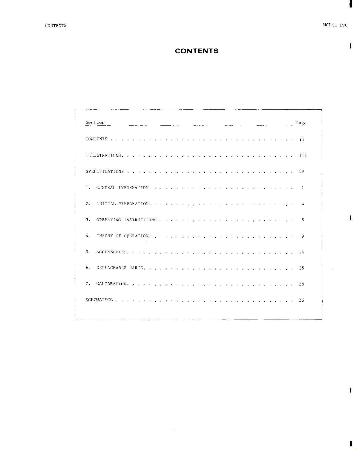
CONTENTS
Page 3
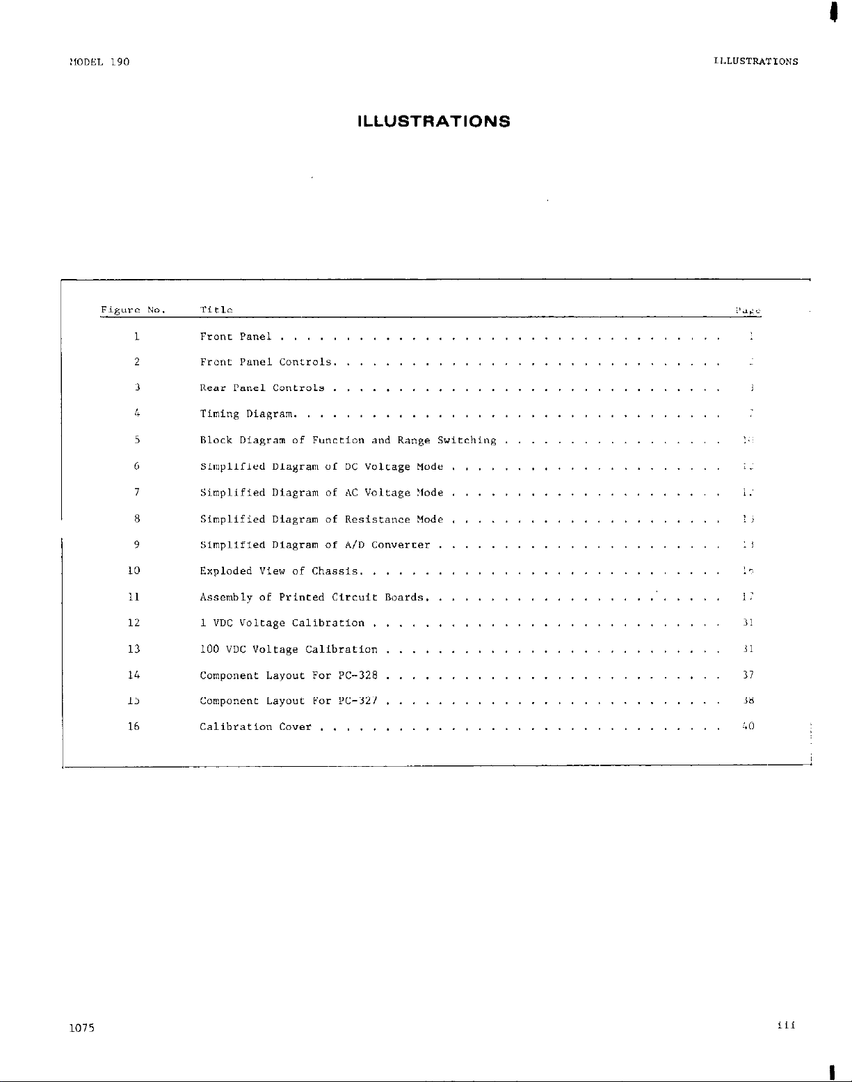
ILLUSTRATIONS
-
1075
Page 4
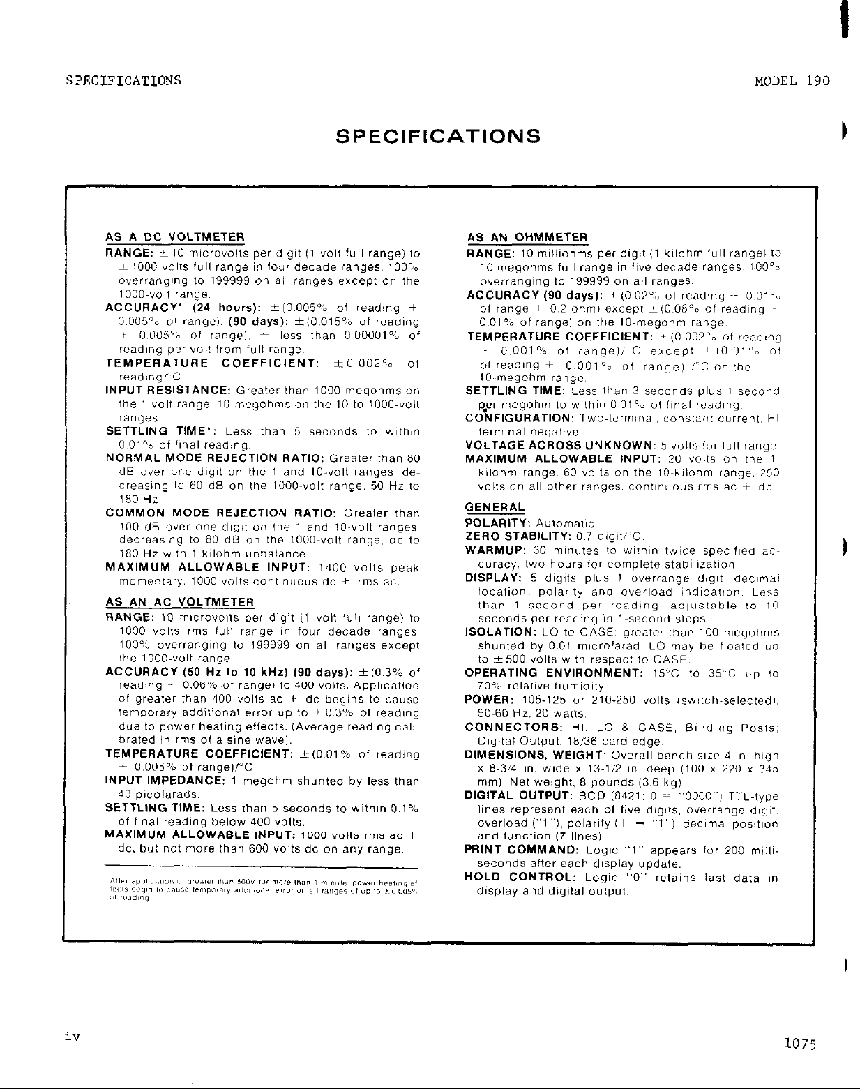
SPECIFICATIONS
MODEL 190
SPECIFICATIONS
AS A DC VOLTMETER
RANGE: -‘lo m~crovolts per d,git (1 volt full range) lo
IlOO volts full range in four decade ranges. 100%
““erranglng to 199999 on ai1 ranges except on the
1000.““II range,
ACCURACY’ (24 hours): 5(0.005% of reading +
0,005”0
i 0,00500 “I range,, * k?ss than 0~00001% Of
reading per ““I, from full range
TEMPERATURE COEFFICIENT: iO,OOZ% “1
readinglc
INPUT RESISTANCE: Greater than 1000 megohms on
the l-V”,, range, 10 megohms on the 10 to 1000.““If
ranges,
SETTLING TIME’: Less than 5 seconds to wfh,n
0 01% Of fInal reading.
NORMAL MODE REJECTION RATIO: Greater than 60
dB ““er one d,g,l on the 1 and IO-““,! ranges. decreasing I” 60 cl8 on the 1000~volt range. 50 Hz l”
180 HZ
COMMON MODE REJECTION RATIO: Greater than
100 dB over one dIgIt on the 1 and IO-““,, ranges,
decreasing to 80 dB “n the 1000-v”,, range. dc lo
180 HZ with 1 kll”hrr ““balance.
MAXIMUM ALLOWABLE INPUT: ,400 volts peak
mome”tary, 1000 ““It* c”ntl”“““S dc + rms ac.
AS AN AC VOLTMETER
RANGE: IO m~cr”v”,ts pei dig0 11 volt (~11 range) l”
1000 ““ifs r”,s ,“I, range in four decade ranges.
100% OverrangIng to 199999 on a,, ranges except
the 1000-“01t range.
ACCURACY 150 Hz to 10 klizl (90 davs,: &10~3% of
reading + 6.06%
of greater than 400 volts ac + dc begins t” cause
temporary additional err”r up 1” *0,3?& of reading
due lo paver heating effects. (Average reading “al!brated in rms of a sine wave).
TEMPERATURE COEFFICIENT: &(O.OI% of reading
+ 0.005% Of rangevc,
INPUT IMPEDANCE: 1 megohm shunted by less than
40 picotarads.
SETTLING TIME: Less iha” 5 sec”nds to with,” 0.1%
of final reading below 400 volts.
MAXIMUM ALLOWABLE INPUT: ,000 volts rms ac +
dc. but not m”re than 600 volts dc on any range.
01 range). (90 days); +(0.015% of reading
of range, tb ho0 wit,: A&xtion
AS AN OHMMETER
RANGE: 10 milliohms per digit (1 lcllohm full range) 1”
10 megohms full range in 11% decade ranges 1,OO”o
overranging lo 199999 on ail ranges~
ACCURACY (90 days): ?tO 02% of readlng + 0 O,“a
Of ranqe + O,2 ohm, exceDt _tio~08”o 0, lead,“” f
O.OlYo-“I range) on the lO:meg;hm range -
TEMPERATURE COEFFICIENT: ?10~002”~ “1 read,“”
1, 0,001% “1 range,/ c except i(0 01”” “‘i
“1 readlng’+ 0.001”~ “1 range) ‘“c “n the
10.megohm range,
SETTLING TIME: Less than 3 seconds plus 1 second
ppr megohm lo wIthin OOlOb of final readlng~
CONFIGURATION: Two-termina,. constant currents HI
VOLTAGE ACROSS UNKNOWN: 5 volts for fu,, ranqe~
MAXIMUM ALLOWASLE INPUT: 20 v”Its “n the-1~
kllohm range. 60 “011s “n the IO-k,iohm range, 250
volts on ail other ranges, c”nf~n~“us rms ac + dc
GENERAL
POLARITY: Automal~c
ZERO STABILITY: 0.7 digif,‘C
WARMUP: 30 minutes 1” within twice spec~hed act
curacy. two hours for complete stabilhzatlon,
DISPLAY: 5 d,g,ts plus 1 overrange d<g,f, decimal
location: polarsty and overload indication Less
than 1 Second per reading. ad,“stable to 10
seconds per reading in l-second steps,
ISOLATION: LO to CASE: greater than 100 megohms
shunted by 0.01 mlcrofarad LO may be floated up
to 2500 volts with respect 10 CASE,
OPERATING ENVIRONMENT: 15’,C to 35-C up to
70Da relative humidity.
POWER: 105-125 or 210-250 ““Its Isw!tch-selected,,
50-60 Hr. 20 watts,
CONNECTORS: HI. LO 8. CASE, B~nd,n” Posts
Digital Output, l&36 card edges
DIMENSIONS, WEIGHT: Overall bench size 4 in, Hugh
x 6-314 I”. wide x 13-l/2 I”. dee” ,100 x 220 Y 345
mm), Nel weight, 6 pounds (3.6 ig):
DIGITAL OUTPUT: BCD (8421: 0 = “0000”) TTL-tv”e
lines represent each of five digits. overrange df’rzit,
overload (“1 “1, polarity (+ = “I”), decimal pos$l!“n
and function (7 lines).
PRINT COMMAND: Logic “1” appears for 200 milli-
seconds after each display update.
HOLD CONTROL: Logic “0” retains iast data I”
display and digital “utput.
iv
1075
Page 5
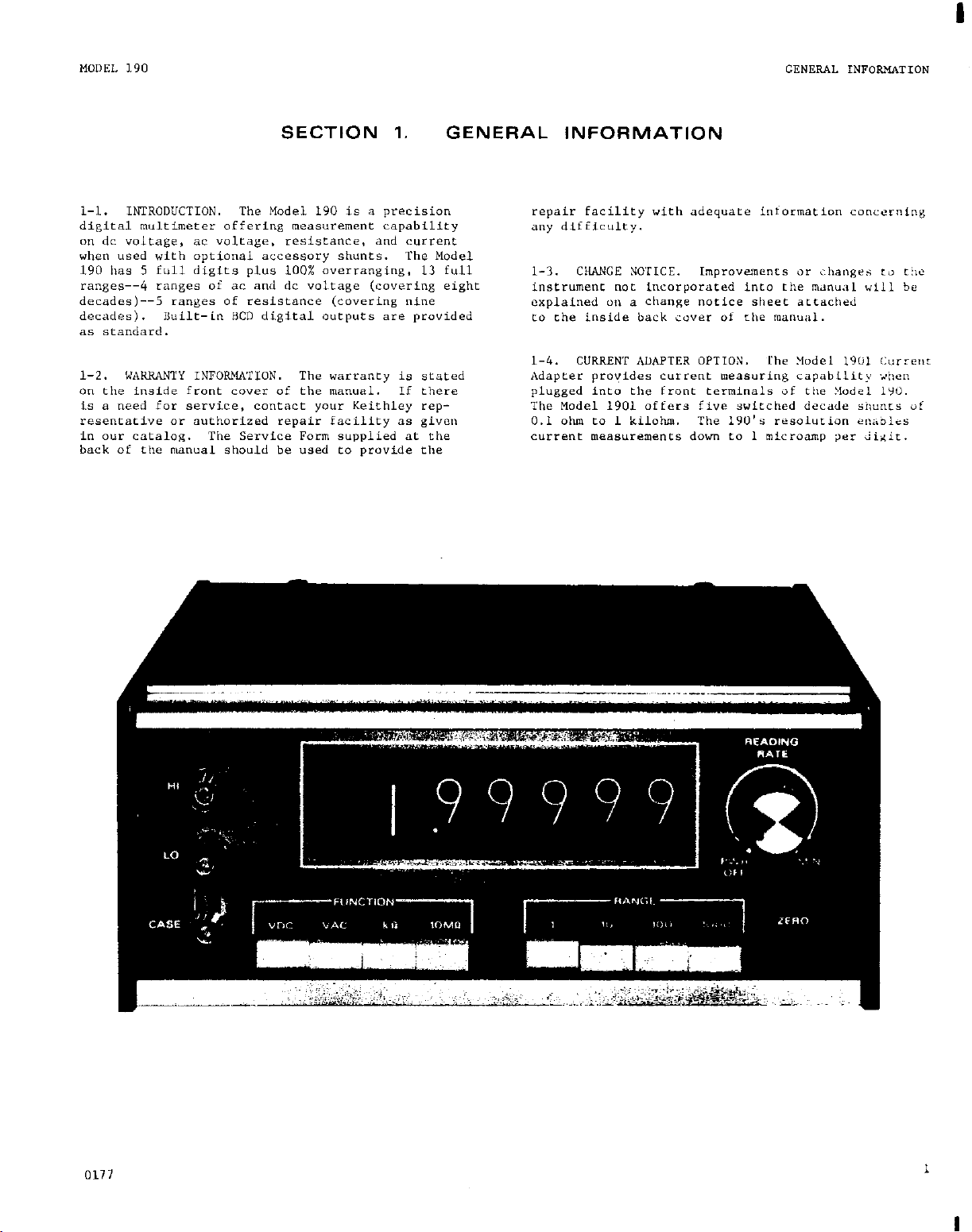
SECTION 1. GENERAL INFORMATION
0177
Page 6
TABLE l-l.
Front Panel Controls
Control
Power Off
Reading Rare
Controls line power to instrument..
Sets reading rate and print rate at digital 3-3b
output.
Functional Description
Variable control from 1 seclreading
(max) ea 10 secslreading (ml”).
Input Terminals
HI:
LO:
Connection to input high for all measurements.
Connection to input law far all. measurements.
CASE: connection to chassis ground. [Shorting link
may be used between I.0 and CASE for grounded
0perati0n.l
Four pushbuttons selecr the desired input mode.
Voltage mode, dc
Voltage mode, ac rms
o,meter mode, ki1ohms
ohmmeter made, ten megohms full range.
Four pushburtons select full ranges for “DC, “AC,
and kn functions only. When IO,% function is
selected all range buttons are released.
1:
10: 19.9999 Decimal
100: 199.999 Position
1000:
1.99999
999.99
I
Zero
Range Multiplier:
Permits adjustment of zero offsee.
Paragraph
2-3d
3-b
~ 3-2
_-
Page 7
Line Switch
Line Receptacle
TABLE 1-2.
Rear Panel Controls
Digital output
+lO” hf. Adjust
Card edge co”nector.
Calibration control.
-10” Ref. Adjust Calibration control.
Page 8
3
MODEL 190
SECTION 2.
2-1.
GENERAL.
incoming inspectim and preparati** for use.
2-2. INSPECTION.
ted both mechanically and electrically before shipment.
Upon receiving the instrument, check for any obv*ous
damage which may have occurred during transit. &port
any damages to the shipping agent.
2-3. PREPARATION FOR "SE.
a. Line Voltage.
the posirion of the LINE switch (S301) on the rear
pa*&.
XI-60 Hz line voltages over the range 105 to 125" ms.
Select the 234V posirio" for operation from 50-60 Hz
line voltages over the range 210-250" rms.
is selected, check for the praper fuse type and rating
as follows:
Select the 117" positia" for operation from
b. Fuse Installation.
This section describes procedures for
me Model 190 was carefully inspec-
Before power is applied, check
After the line voltage range
111v: 1/4A (N-17)
234Y: ll8A
@lJ-20)
INITIAL PREPARATION
C.
Line Connection.
three-wire line card (Keithley part no. U-7) Which
provides connections to line power (high, c"mo", and
chassis).
pin should be connected to earth ground.
above chassis ground, make certain that the
"link" between LO and CASE on the front
pane1 is removed.
d.
racy requires a warm-up time (with pnwer on) af tw"
hours.
ternal circuitry has reached a temperature equilibrium. Ambient temperat"re variations afier sebiiizatio" mu~st be considered usFng the appropriate
temperature coefficients for each functLo*.
e.
vo1ra.w measurements, check the zero reading on the
l-volt range by connecting a low-thermal short across
the input terminals. Adlust the fmnt panel zera
control CO obtain a zero reading such that the "minus"
polarity sign flashes on and off.
For operator safety, the chassis ground
If the Fnstrwnent input LO is to be floated
Warm-up. Complete stabilization to raced accu-
This time is required to ensure that the in-
Zero Adjusment. To achieve rated accuracy on
This instrument requires a
1
4
Page 9
MODEL 190
A
SECTION 3.
OPERAT’ING INSTRUCTIONS
overrange
Display
1.99999 "
19.9999 v
199.999 "
1000.00 v*
*Maximum allawable input: 1400 ” peak mOme”tarV
Connections. Make connections to the input HI
a.
and LO terminals.
terrain chat the shorting link is connected between
LO and CASE.
link must be removed.
b. Control Secfi”,Qs. To select the dc voleage
.ode, depress the “DC pushburton. To select the full
range sensitivity, depress the appropriate range pushbutton, 1, IO, 100, or 1000. Adjust the Reading Kate
to achieve the desired display rate.
For grounded applicationa, make
For floating applications, the shorting
1073
Page 10
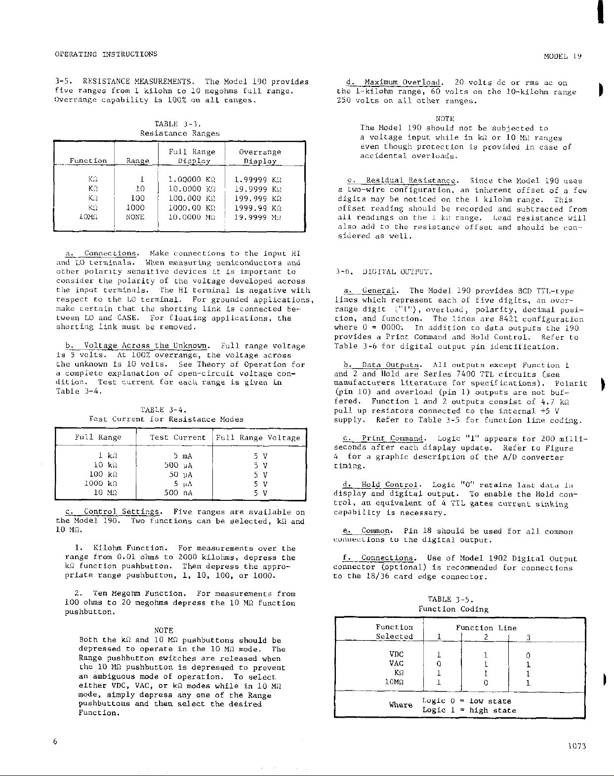
3-5. RESISTANCE MEAS”REMENTS. The Model 190 pravides
five ranges from I kilohm to 10 megohms full range.
tierrange capabiLity is 100% on all ranges.
d Maximum Overload. 20 “OltS dc or rills ac “1,
the I-kilohm range, 60 volts on Lhe IO-kilohm range
250 Volts on all other ranges.
TABLE 3 -'I.
Resistance Ranges
I
‘- Connections. ELake connections to the input HI
and LO terminals. When measuring semiconductors and
other polariiy sensitive devices it is important to
consider the polarity of the voltage developed across
the input terminals. ‘The HI terminal Fs negative with
respect co the 1.0 terminal. For grounded applications.
make certain chat the shorting link is connected between LO and CASE. For Elmring applications, rhe
shorting Link must be removed.
b. Voltage *cross the U”k”0w”. Full range “alrage
is 5 volts.
the unknow” is 10 volts. see Theory of operation for
a mmplete explanation of open-circuit voltage condition. Test current for each range is give* io
Table 3-4.
At 100% overrange, the voltage across
TABLE 3-4.
‘Test Current for Resistance Modes
The Model 190 should not be subjected to
a voltage input while in 102 or 10 MI1 ranges
even though protection is provided in case of
accidental overloads.
e.
Residual Resistance. since the ?kdel 190 uses
B two-wire configuration, an inherent offset of a few
digits may be noticed on the I kiloiun range. This
offset reading should be recorded and subtracted from
all readings on rile 1 k>C range.
also add to the resiscancr “ffset and should be co,,sidered as well.
a.
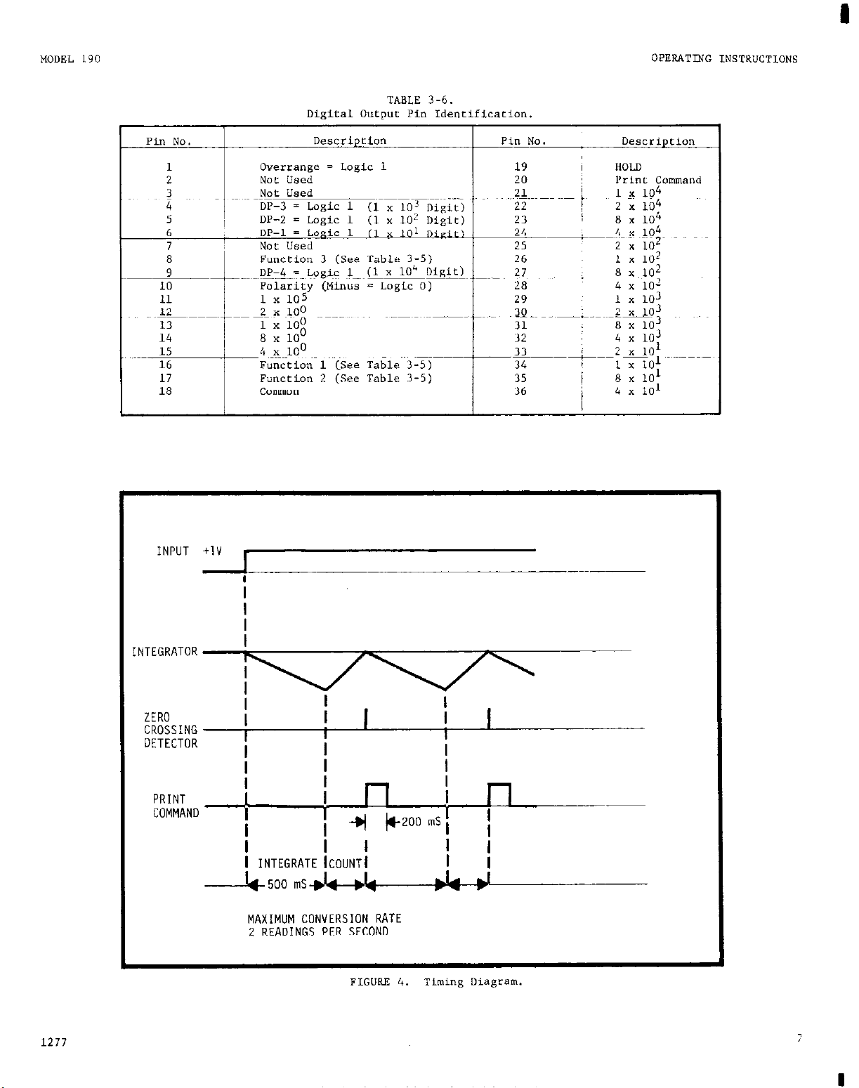
General. The M”del 190 provides BCD TX’,.-type
lines which represmt each of five digits, an overrange digit i”“), overload, polarity, decimal position, and function. The lines are 8421 configuration
where 0 = 0000; I” addition LO data outputs the 19”
provides a Prinr ~omand and ilold Control. Refer to
Table 3-6 for digital output pin identification.
b. Data outputs.
and 2 and Hold are Series 7400 TTL circuits (see
manufacturers literature for specilications). Polarit
bin 10) and overload (pin 1) outputs are “ot buf-
fered.
pull up resistors connected to the internal +5 V
S”PPlY,
Function 1 and 2 outputs consist of 4.7 kii
Refer to Table 3-5 for function ltie coding.
NOTI:
Lead resistance will
All outputs except runcti”” 1
Full Range ‘rest current Full Range Voltage
I
C.
Control settings. Five ranges are available on
the Model 190.
1” m.
1.
Kilohm Functian. For measurements over the
range from 0.01 ohms to 2000 kilohms, depress the
kD function pushbueco”. The” depress the appropriate range pushbucto”, 1, 10, 100, or 1000.
2. Ten mgohm Function. For meaSureme”tS from
100 ohms eo 20 megohms depress the 10 MS? function
pushbutton.
Both the kQ and 10 Mn pushbuttons should be
depressed to operate in the 10 Mn mode. The
Range pushbutton switches are released when
the 10 Mn pushbutfm is depressed to prevent
an ambiguous mode of operation. To select
either “DC, “AC, or kn modes while in 10 MQ
mode, simply depress any one of the Range
pushbuttons and then select the desired
F”“Cti0”.
‘TWO functions can be selected, kC# and
NOTE
C.
erinr: Command. Logic “1” appears for LOO milliseconds after each display update.
4 for a graphic description of the A/D converter
timing.
d.
Hold Control.
display and digital oufput.
tro1, an equiva1enr of 4 TTL gates current sinking
capabiliry is necessary.
e.
COMnO”. Pin 18 should be used for al.1 cmn,,~”
connections to the digital ““tput.
f. Connectians. Use of Model 1902 Digital outp,,t
connecfor (optional) is recommended for connections
to the M/36 card edge con”ectar.
F”“C?ZiO”
Selected 1 2 3
“DC 1 1
“AC 0 1 1
KG 1 1 1
lam 1 0 1
mere Logic 0 = 10” state
Logic “0” retains last data in
To enable the Hold co”-
TABLE 3 -5.
Function Coding
Functia” Line
Logic 1 = high state
Refer to Figure
0
6
Page 11
INPUT +lV
I
1277
INTEGRATOR
ZERO
CROSSING
DETECTOR
PRINT
COMMAND
I
i
I
I
I
I
I
MAXIMUM CONVERSION RATE
2 READINGS PER SECOND
I
I I
I
Page 12
p
OPERATING INSTR”CTlONS
3-7. MEAS”REMENT CONSI”EFATIONS
a.
connections.
recommended when source resistances are greater than
1 kihhm or when using the 10M.Z mode.
be exercised so as nof to degrade the insularian
characterisrics Of the binding posts.
tance modes, accuracy may be degraded if the eerminals
and/or leads become contaminated. care should also be
take” fO minimize effects of thermoelectric porcntia1.3
which may be generared as a result of temperature
differences between junctions of dissimilar metals.
1. DC Voltage. me dc voltage accuracy is
specified in terms of a percent of reading and a
percent of range. An additional factor of .OOOOl%
of reading, per volt from full range reflects an
uncertainty due CO voltage coefficients for measurements made at “ther than fuU range. Short term
accuracy is valid for a period of 24 hours afrer
complete calibration. Long term accuracy (90 days)
includes an additional .Ol% of reading uncertainty
due to aging of precision components.
the effects of power dissipated in the input resist”rs should be considered whenever more than 500
volts is continuously applied (for 1 minute or
longer). Heating may cause a* additional uncertain-
ty due to the temperature coefficients of individual
circuit elements.
“se of shielded input leads is
care should
In the resis-
In addition,
MODEL L90
3.
AC Voleage.
specified in terms of a percent of reading and a
percent Of range. In addition, the effects of
power dissipated in the input resistors stm~ld be
considered whenever more cllan 400 volts is applied.
4.
Resistance. hccuracy on IeSiStanCC ranges
is specified in terms of a percent of reading and
a percent of range. An addieional uncertainty due
to residual resistance should also be considered.
when making resistance measurenlents, ic is
important- co make certain that t’he 190 is
properly zeroed in “DC function. Fur example
an additional error of .OOOl% of reading can
occur per digit of voltage offset on the Ik:;
- loom ranges;
per digit offset on lOOOkG and 10MI: ranges
respectively.
The ac voltage accuracy is
NOTE
.OOl% and .Ol% of reading
2. DC Current. When tire Model 1901 Currenf
Adapter is used an additional iO.3% of reading
uncertainty must be considered. As in any current
measurement the input drop should also be consider-
ed.
For example, a full range drop of 200,“”
across the shunt results in an error of 1% if the
source is 20 volts.
017 7
I
Page 13
MODEL 190
I
THEORY OF OPERATION
SECTION 4. THEORY OF OPERATION
4-L. GENERAL DESCRIPTION. The Model 190 Digital
nulrinieter utilizes a modified integrating technqiue
ior A/O CO""erSio".
integrated circuits are utilized for greater reliability and servicing. The circuitry is broken down
into two major areas and assemblies; fbe Analog
Assembly and Digital and Power Supply Assembly.
'me halog section provides input signal conditioni"g,atte"uatio", filtering, buffering comparixg, and
initiates the main control signal for the entire
system. The Digital section provides logic control,
counting, decading and display. Usa located on tke
Digital assembly are the power supplies far the entire
system.
Digital assembly thraugh 5301 and 5302.
TO follow through a block diagram description it will
be necessary to make several assumptions; assume the
display is reading 0.0000, the counters have bee" re-
set LO zero, the a"alag switch, Sl (Q117) has jut turned
on allowing ihe integrator to sample the voltage at
Lhe input terminals. A voltage of +lO MC is applied
.o the input terminals.
to the DC attenuator and divided t" 1 VDC which
gpasses through the filter section LO bypass any AC
compooenc t" common.
tion is applied co the input amplifier section whick
provides signal isolation and a fixed gain of 5. The
mplifier signal, now at 5 "DC, is applied CO the
hregrarar section via Sl (Q117), Analog Switch. The
analog Switch has been turned o" by a control level
provided by circuitry, (the primary control flip-flop),
in the Digirvl Hssembly.
signal causes the integrating capacitor, C141,,to
charge for a fixed period of time, (approximately
500 milliseconds), or 200,000 counta. The final
count pulse clears the COunrerS to 0.0000. AT the
end of this period of time, a combinaeia" of a lo&
level at the zero detector amplifier, and the resef-
ting of the primary control flip-flop, causes S1
(Q117) Analog Switch, to turn off and 53 CQ116),
minus Reference switch, to turn on. The counter
starts counting towards 200,000 again. With a minus
input from the reference now applied to the Integrat-
ing hplifier, C141, begins t" discharge towards zem.
Upon reaching zero ""its, the zero detect"= Amplifier
creates a logic pulse that stops the counter which
due t" the relationship of the Integrator and clock
has counted t" 100,000.
control far the lagic, it is gated to farm a strobe
far the storage section. Information prek?ent in
storage is now made available t" the decoder section
which furnishes levels that light the display with
the counted "umber 100,000. A delayed strobe pulse
fallows within 1.0 microsecond which resets the
counters to zero, and resets the primary central
flip-flop.
Swirch, to turn off, and S1 (Q117) Analog Switch, t"
turn 0".
The Analog assembly is connected t" the
This3 causes s3, (9116) minus Reference
The latest linear and digital
me 10 volt signal is routed
The output of the filter sec-
Application of the +5V
This pulse becomes a primary
4-2. ANALM: ASSEMBLY. The following paragraphs describe individual Analog circuits in detail. These
circuits are divided according t" their primary
function in rhe system. (Refer to Schematic 25864E).
a. DC Atfenuafor.
P.118, and parts of 5102 and 5101, pravides artenuario"
for input signals above 2 VDC (100% overrange on the
1 " range).
impedance for better input matching a" the lowest
dc range.
b. Input Filter.
tion of ac components and noise present on dc input
signals.
C. InpuL Amplifier.
ponents, this circuit provides input isolation and
signal conditioning. 4119 ii; a low leakage matched
Fl?r providing high input impedance and matched voltage and temperature tracking. A bipolar device, "UCputs from this FET are applied directly at Q*101, a"
operarional amplfier.
variable resistor, is used for initial balancing of
inpw PET pair while Q106 provides a canstant curre"~
source. 0119 and QAlOl, a" IC Operational Amplifier,
provide the gain required by the Input DC Amplifier
The maximum output swing at the Input timplifier, TP1,
is 210 MC. This output is fed directly to 9117, the
Analog Switch. P"te"tiometer R155, front panel zero,
is used for fine zer" adjustment.
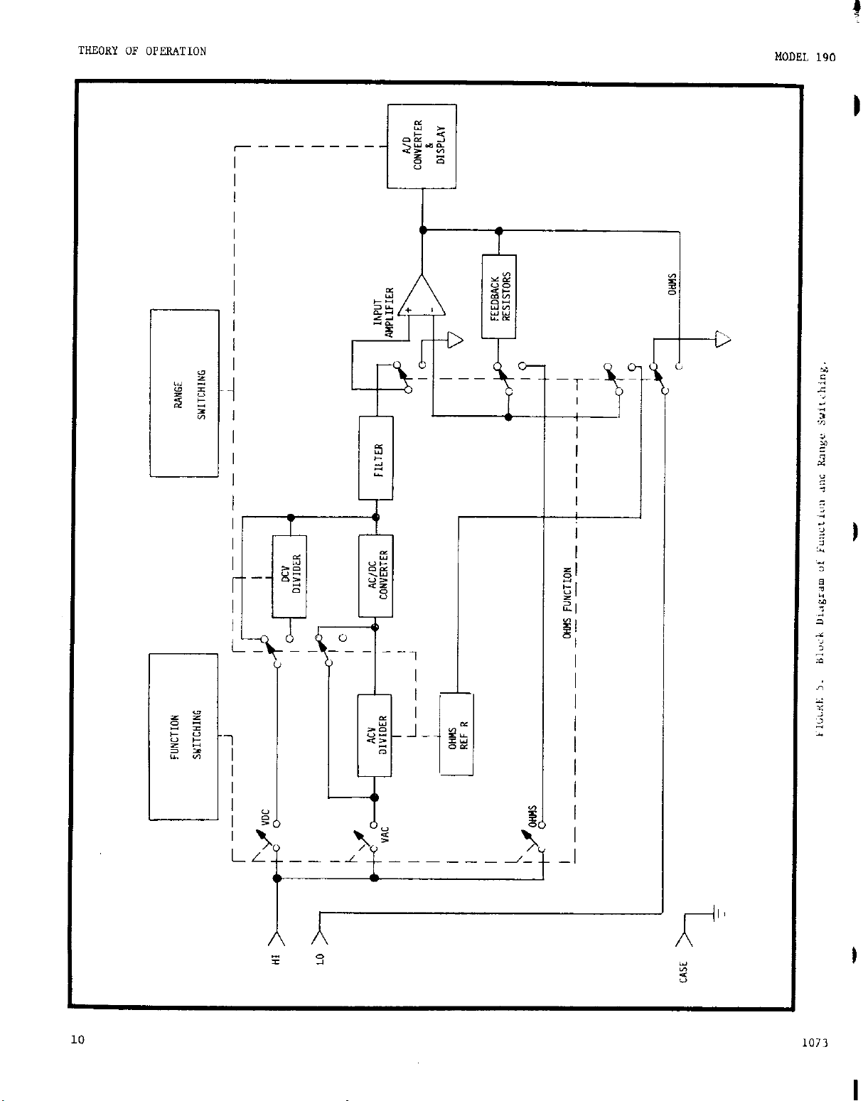
d. Signal Switches (See Figure 5).
q110, Ql16, and Q117, these solid state switches
provide high speed, low leakage paths for signals
applied to the Integrating Amplifier. These switches
are drive" by logic levels fram the Digital Assembly
with Q109 and Qlll through Q115 supplying buffering.
e. Integrating Amplifier. Also a bipolar circuit
this Amplifier integrates dc levels fram signals applied through S1 (41171, 52 (QllO), and S3 (9116). A
unity dc Cain Amplifier, rhe precision ramps created
by the time c""stants of RI01 and Cl41 are directly
proportional co the clock speed in the Digital Section.
Using a modified dual slope principal, the charge
time of Cl41 is fixed at appmximately 500 ms, while
the discharge time is a function of the input voltage.
The maximum swing at the output of this amplifier,
TP4, is approximately t12 v peak. The output is fed
dir-ect1y to the comparator.
f. Zero Defecfor - Comparator. This circuit
creates the main control pulse and logic level necessary for proper digital and analog functions.
an IC Operational Amplifier, provides a dc gain ior
signals less than +I00 uV. The level at the output
of QA107, is determined by the polarity of the unknown
5102-30 is used to shart "ut the higb
A 10 megohm divider using RIII-
This section provides attenua-
Cmprised of rhree acti"e com-
R146, (Coarse Zero) a 100 :!
Comprised of
QA106,
1075
9
Page 14
THEORY OF OPERaION
MODEL 190
10
Page 15

Page 16

HI
INPUT
TERMINALS
LO
DCV DIVIDER FILTER
r-------
1 VDC
10
"DC
11
100
WC
1----
T’VVG I
9
1000
P
WC
i
- --
INPUT AMPL[FIER
T--~-----I
TO A/O
CONVERTER
>
RI56
r----
FIGURE 6.
ACY OIYlDLR
-------
SimpLifFed “iagram Of DC Voltage Mode.
AC,DC CONYtRTOi
r----
---_
----r----i
FILTER
1073
I
Page 17

I I
lkn
2kn
CONVERTER
1073
FIGURE 9. Simplifiad Diagram of A/D converter
Page 18

SECTION 5. ACCESSORIES
5-s. GENERAL.
be used with the Model 190 eo provide additional con- Manual is supplied witi, eacn accessory giving complete
venience and versatility.
The following Keithley *cces~ories can 5-2. OPERATING INSTK"CTIONS. A separate 1nsrruction
operaring information.
Modes 190s current Adapter
Description: Application:
Five Switched decade shunts of 0.1 ohm to 1 kilohm
50.3%. Maximum continuous voltage drop is 7.00 rn". of the 190 to measure currents up to 200 rd. Adapter
Shunt resistors are connected so as to eliminate con- plugs into input terminals.
tact resistance errors.
Modes 1902 Output connector
Description:
Mating card-edge ~"nnector for digital output (18136
pins).
of the 190.
connector plugs into card edge at rear panes
Model 1903 Calibration cover
me Modes 1901 muy be used on ac an* dc voscagr rnnges
Application:
Provides access to ass 36 pins at digital ""tpuits.
Enables CUStom wiring to digital printers or other
digital acquisition equipment.
Application:
Used whenever calibration adjustments are necessary.
Confrols are identified by circuit designation as
shown OrI schematics.
14
1073
Page 19

SECTION 6.
REPLACEABLE PARTS
Page 20

REPLACEABLE PARTS
I
-- Chassis Assembly
1 Side Panel, Left
2 Side Panel, Right
3 Rear Panel
4
5 O”erlay
_-
6 Top Cover
7 Bottom ccmer Assembly
^-
-- Tilt Bail
-- Feet, Molded
_-
8 screw, Flat Phil. Hd.
9
10 Buttons, white
Front Panel
Will&J”
Bottom cover
Rubber Ball
Knob Assembly t
-1
1
1 25840B
I 2583OC
1
L
1
1
1
1
4
4 FE-6
4
8
25859A
25832C
258608
25843A
25836C
25846B
25835C
24879B
243228
116-32 x 5/W
25151A
--
-_
16
1073
Page 21

1073
17
I
Page 22

Mfr.
oesig.
Keithley
Pare No.
.8-U DF. “AR .
33 pF, 500", Mica
.8-l* pF, "AR
390 pF, soov, Mica.
.8-12 pF, "AR . .
4700 pF, 500", Mica
.Ol uF. 6OOv, PolyP
2 pF, 500", pica. .
2 PF, 500", Mica.
.a-18 pF, 750", via
4.7 "F. 20". WT.
4.7 pF, zov; ETT.
56 UF, ZO", ETT .
100 pF, 500". Nica.
20 p, 500", Mica .
100 p, 15”, Epoxy.
2.0 UF, 50”, Mx. .
0.1 gF, 250", MtF .
1.0 uF, 5O", MtF. .
0.22 PF, 250", MtF.
0.1 UF, 250". MfF
,047 UF, ZOO", MFCb
.047 pF, ZOO", MPCb
0.01 pF, 500", CerD
0.1 "F, 250", MtF .
.Ol UF, 500”, cero.
.047 IIF, ZOO”, MPCb
.Ol IJF, 500", CerD.
0.1 uF, 250", MfP .
Not "sed. .
.
. .
. .
.
. .
. .
. .
. .
. .
.
.
.
.
. .
.
.
.
.
.
.
.
.
.
.
.
.
.
.
.
. .
.
.
. .
.
.
.
.
.
.
. .
.
. .
.
. .
.
.
.
.
.
. .
. .
.
.
. .
.
.
. .
.
. .
.
.
.
73899
14655
73899
14655
73899
14655
97419
14655
14655
72982
17554
17554
17554
14655
14655
17554
14752 625BlA
73445 C280AE
14752
73445 C28OAE
73445
14752
14752
72982
73445
72982
14752
72982
73445
. . . .
5C154Y
CDlOED330J03
5C154Y
CD19ED391J03
5C154Y
CD19ED471JO3
M2WFO.l~F
CD10CD020D03
CD10CD020D03
567-013
TSDl-20
TSDl-20
TS”l-20
CDLOED101J03
CD10ED200J03
TD5-015-107-10
625BU.105
C280AE
62581C473
625BlC473
871-25"0103M
C280AE C178-.LM
871-25"0103M
625BlC473
871-Z5"0103M
C280.G
. . . . . .
c253-.8-12P
C236-33P
c253-.8-12P
C236-39OP
C253-.R-12P
C236-47OOP
c**o-0. lM
c231-2P
C231-ZP
c225-.8-18P
c179-4.7x
C179-4.7M
C179-56M
C236-1OOP
C236-2OP
C228-1OOM
CZOl-2.OM
C178-.LN
c215-1.011
Cl,&.22M
C178-.LM
C221-.047M
C221-.047M
c**-.olM
c**-. OlM
C221-.047M
c**-. OlM
CL78-0.0,
. . . .
0.1 IrF, 250”, MCF
4.7 UF, ZO", ETT.
33 DF. 1000". CerD.
O.l'~i, 25OV; MtF .
33 pF, lOOO", cem.
.oo** pF. 1000”, CerD ................
.0022 UF, lOOOV, cero ................
20 PF, soov, Mica ..................
20 PF, 5oov, Mica ..................
20 pF, 500", Mica
1.0 VF, loo", Poly. .................
0.1 uF. 250", MtF ..................
33 pF, lOOO", cero. .................
0.1 LIF, 250", MfF ..................
0.1 uF, 25OV, MtF ..................
Not Used. ......................
NOf Used. ......................
0.1 !S, 25OV, MtF
5 pF, lOOO", cero ..................
0.1 UF, 25OV, MfF ..................
..................
..................
. .
. .
.
.
. .
. .
.
.
. .
. .
73445
17554
71590
73445
71590
56289
56289
14655
14655
14655
97419
73445
71590
73445
73445
. . .
.
73445
71590
13445
c**oAE
TSOl-20
m-330
C28OAE
m-330
LOSS-022 C64-.OO**M
loss-D** C64-.OO**M
CD10E0200J03 C236-2OP
CD10E!x00J03 C236-2OP
CD10ED200J03
PYW-R (1.0)
C280AE
"O-330
C280AE
C280AE
CL78-O.LM
C179-4.7M
C64-33P
C178-O.lM
C64-33P
C236-2OP
C142-l.OM
C178-o.lM
C64-33P
C178-0.m
C178-O.LM
. . . . .
. . . . . . . .
C280AE
m-050 C64-5P
C28OAE
. . .
C178-0.1M
C178-o.lM
Page 23

‘\Nb.LOC SECTION (Coni’d)
(Schematic 25864E)
CAPACITORS (‘zont’d)
CiITtliC
IkSiR. Description
Cl51 0.1 iiF. 250", XCF
Cl52 .oo** JF, IOOO", Cer"
Cl53 0068 PF, 500", Cer". .
Cl54 150 pF, IOOO", CerD . . ~
Cl55
Cl56
Ill01 Transistor,
"102
"103
0104
D105
0106
0107
D108
DlO9
DllO
Dlll
0112
0113
0114
D115
150 pF, lOOO", certl . . . . . .
5
Transistor, NPN, Case TO-106. .
75" PI", 75 Ill‘, ....................
75VPIV.75~ .................... 01295
75YPI", 75~ .................... 01295
Zener, 6.3V, 1/4W ..................
75V PIV, 75 n*. ...................
15" PI", 75 nut. ...................
75"PI".75mA .................... 01295 lN914
75v PI", 75 !A. ................... 01295
1000", cem .
PI?,
NPN, Case 'R-106. ............ 07263
Mfr.
Code
73445
56289 loss-LIZ?
72982
71590 DO-151
71590 W-151
71590
07263
01295
N-C
01295 IN914
01295 IN914
01295
01295
01295
01295
01295
>,tEr.
oesig.
-
C?ROAE
d51-25U"-682~
La-050
2N3565
2X3565
IN827AX
lN914
IN914
I%914
1N914
lN914
0116
"117
D118
0119
0120
0121
.JlOl Binding Post (Red) HI
.I102 Binding Posf (Blk) LO
5103 Binding Post (cm) CASE
M-C = MICROSEMICOND”CTOR
0177
.....................
.....................
....................
12954
. . . .
06751
06751
01295
01295
Mfr. Mfr.
lN706
IN703A
1N70JA
lN914
13914
820-65
RZO-45
820-95
-
Page 24

ANALOG SECTION (Cont’d)
(Schematic 25864E)
TRANSISTORS
Mr.
CO&
N-Ckm FET, case TO-72.
NPN, case TO-92 .
NPN, case TO-92
NPN, case TO-92
NPN, case TO-92
NPX, case TO-92
I's*, case 'CO-92
NPN, case 'TO-92
NPN, Case TO-92
?I-Cha*, J-FET, case TO-18
PNP, case TO-92
NPN, case TO-92
FNP, case TO-92
NPK, case TO-92 . . .
PXP, case IO-92
N-Ghan J-FET, Case TO-18. .
N-ma" J-FET, case TO-18. ,
PNP, case TO-92 . .
Dual wchan J-FET, case TO-71
.
.
. .
I
. .
. .
04713
04713
04713
04713
04713
04713
04713
04713
04713
32293
04713
04713
04713
04713
04713
32293
32293
04713
32293
INTEGRATED CLRCUITS
QAlOl Operational Amplifier, 8-pin, Case TO-99. 24355
QUO2
Qb.103 Operaeional Amplifier, 8-pin, Case TO-99. . . . . . .
Not Used. . . .
12040 LK308"
2N4220
2N5089
2N5089
2N3903
2N3903
2N3903
2N3905
ZN3903
2N3903
ITS3538
au905
2N3903
*I?3905
2N3903
2N3905
ITS3538
1153538
2N3905
ITS30092
Mfr.
Iksig.
m741*
TC-42 i
W-62
TC-62
TG-49
'X-49
n-49
K-53 5
'U-49
'R-49
V-88
‘R-53
x-49
x-53
TG-49
'U-53
X-88
P-88
K-53
TC-9R
IC-97 1
K-67
2
7
1
1
1
Quo4 Operational i\mplLfier* 8-pin DIP. . . . . . .
QR.105
QUO6
Operational Amplifier, 8-pin DIP. . . .
Amplifier, 8-pin, DIP . . . . . . . 12040
Q.&l07 Amplifier, 8-pin. DLP . . . .
*Selected, order by Keifhley Part NO. IC-97.
SlOl
s102
Switch, Function. ........
SWitCh, Range ..........
.........
.........
20
32293
32293
ITS6214
ITS6214
LM30L4N
12040
80164
LM301AN
SW-370 Ilront Panel
80164 SW-369
n-74
K-74
ic-24
K-24
2
2
Front Panel
1075
Page 25

ANALOG SECTION (cont’d)
(Schematic 25864E)
RESISTORS
RlOl
RlOZ 1 M!1, ".5%, ZW.
R103
RI04
RlO5 1 MQ. 0.5%. 2w. . . .
R106
RIO7 200 !2, 0.5w, "AR. . .
11108
Rl09 992 !1, O.l%, l/ZW, MLF. .
RllO
Rlll
K112
~ R113
RI14 931 KC, I%, L/8W, MtF . . .
R115 10.11 Kn, 1/4w. . .
*Matci,ad set, order only as a yroup of 4 resiscor5.
~~.~
‘~RT16
K117
R118
11119
R120
K121
I+122 1 MS, 0.5%, zw. .
R123 121 K!, O.l%, 1,*&l, MtF
RI24
Ill25
K126 60.4 Kn, I%, 1/8W, MtF.
R127 2.2 wi, lO%, 1/4w, Camp . .
K128 150 Krl, 10%. lf4W. Camp
R129 680 n, lo%, l/4!.!, Camp.
K130 10 m, lO%, 1/4w. camp.
470 K.., LO%, 1/4w, camp . .
121 K!!, 0.1%. l/ZW, MtF .
2 ~2,0.5W,"N(...................
10 1c1, O.l%, l/ZW, MU.
i "Cl, 0.5%, 2w. .
20 i!, 0.5w, "AR. . , . .
10 M!i, zw .~ . . ., .
1.11 Pm, 1/4w . , . .&&.s.y.aL; ..e-+.
100.91KQ, 1/4w. .
2 iL'1, 0.5w, vi? :. :.
200 2, ".5W, "All.
200 &I, 0.5w, "AR
470 K;1, lO%, IY, camp .
470 K;;, 10%. l/ZW, Camp
470 ui, lO%, 1w, camp
.
.
49.9 &I, 1%. 1/8W, MtP.
LOO K!1, lO%, 114w, camp
.
I
.
01121
"3888
91637
73138
03888
91637
73138
03888
91637
73138
03888
03888
03888
07716
03888
.
.
R0294
80294
80294
01121
01121
01121 G”-470K-10%
0,888 P?IE75 (1X)
91637
0,716 cc\-To-49.9K
OLlZl cB-104-10%
07716
01121 c8-*22-10%
01121
01121 C"-681-10%
01121 CB-103-10%
XFF-IZIK
CEA-TO-60.M
cB-lss-lo%
R76-?.?K
R76-1506
R76-68"
R131
R132
RI33
R134
R135
~136
R137 180 Kn, lO%, 1/4w, camp .
R.138 20 Kn, O.l%, 1/8W, MLF. .
R139 1.15 KO, O.l%, 1/8W, MU.
R140
R141 selected value*, I%, ilaw, MLF. .
RI42
R143 470 Kn, lo%, 1/4W, Camp . . .
El44
RI45 10 K.o, l%, 1/8W. MtF. . .
Kl46 100 n, 0.5". "AR. . . . . . . .
El47 30 KG, .02%, .3w. . . . . .
x14.3 100 Kn. 1%. 1/8W, MtP . . . . .
R149 30 i(R, .02%. .3w. . . .
Kl50 39.2 Kn. 1%. 1/8W. MtF. .
1075
150 ICI, lO%, 1/4W, camp
1.8 m, 10%. 1/4w, comp
680 12. 10%. 1/4w, camp. .
680 0, 10%. 1/4w, camp. . .
3.9 KG, lo%, 1/4W, camp .
232 Kn, l%, 1/8W, MtF
20 II, 0.5w, "AR . .
270 Kn, 10%. 1/4W, Camp . .
14 Ia, l%, l/NJ, MtF. . . . .
.
.
.
.
. .
.
.
.
.
. .
.
. .
. .
.
.
. .
. .
. .
.
OllZl C&154-10%
01121 c*-182-10%
01121 CR-681-10%
01121 CR-681-l"%
01121
07716
01121
91637
91637
73138
07716
01121
01121
07716
07716
73138
18612
07716
18612
07716
a-392-10~~
CF.&-TO-L?ZK
C&184-10%
XFF-l/R-201;
?lFF-lj8-1.1x
72PMR-20
CF.!.-TO-*
CB-274-10%
CB-474-10%
CEA-TO-14K
CW-TO-1OK
IZPMR-100
"53-l-3OK
CEA-TO-IOOK
"53-l-30K
CL&-TO-39.2K
Pm-*
R76-L70K
R76-470X
K88-ILK
K88-10K
RP97-100
R181-3°K
KM-10°K
R18,-101:
R88-,9.:K
Page 26

ANALOG SECTlON (Cone'd)
.
(Schematic 25864E)
RESISTORS (Cont'd)
MODEL 190
R151
R152
R153
RL54
ill55
K156
R157
R.158
R159
Rl60
lu61
R162
R163
R164
R165
R166
R167
R168
RI69
8170
It171
R172
Rl73
RI74
*75
R176
RI77
R178
R179
Rl80
68On, lo%, 1/4W, Camp . . .
68On, 10%. 1/4W, Camp
9.997Ks1, 0.02%, 0.3w. . . .
Not Used. . . . . .
Em, 0.75W, "AR .
10.0, 0.5w, "AR.
Not Used. . . . .
*.5&J, 0.02%. 0.3w. .
47m. 10%. 1/2w, camp
2101, O.Ol%, 0.5w, LWF
2oKn. 0.01%. 0.3w .
2oola, O.Ol%, 0.75w, MtF
*oKn, 0.02%, 0.3w
202.7Q. 0.02%. 0.3w .
30.1m, 1%, l/a?, MtF
zoom, 0.5w, “AR. . .
*.242m, 0.02% 0.3w . I .
1on, 0.5w, "AR. . . . .
NOf Used. . .
Not Used. . . . .
Not Used. . . . .
NOf Used. . .
Not Used. . . . . . . . . .
Nor Used. .
Not Used. . . . . . .
4.7m, lO%, 1/4w, camp. .
Not Used. . . . . . . . .
Ml, I%, l/&l, MtP. .
Selected Value, O.l%, 1/m.
68Oll, 10%. 1/4W, cm* . .
. .
.
. .
. .
. .
. .
. .
. .
. .
. .
. .
. .
01121
.
.
.
. .
. .
.
.
.
. .
. .
. .
01121
18612
73138
73138
. . . .
18612
01121
18612
18612
18612
18612
18612
07716
73138
18612
73138
.
. .
. .
. . . . .
. . . . .
CB-681-10%
CB-681-10% R76-680
"53-1-9.99X-.02% R183-9.997h
.
89P (1KQil)
72PMK-10 RP97-10
. . . . .
v53-l-2.5K-.02%
m-473-10%
V53-5-2K R214-2K
v53-l-*o&c-.01% R184-20R
V53-6-200K
v53-1-2oK-.o*% R183-2OK
V53-l-202.7-.02% R183-202.7
CFA-TO-30.m R88-30.X
72PMR-20OK RP97-200K
"53-I-2.24*1(-.02% R183-2.242X
72nlR-10
. . . . .
. . . .
........
R76-680
RP96-1K
R183-2.5K
RI-47K
K215-ZOOK
8P97-10
.........
........ .........
.
.
. . . . .
.
. .
. .
.
01121 CB-47*-10% R76-4.X
. . . .
07716
91637
01121
........ .........
........ .........
........ .........
. . . . . . f..... . .
CEk-TO-1K R88-1K
Mm-118 R168-*
CB-681-10% R76-680
R181
Kl82
Rl83
R184
RI85
R186 Selected Value, O.l%, l/SW.
xl87 1.*Kn, 10%. 1/4w, camp. . .
Ku38
R189
xl90
8191
lug*
PJ93
Rl94
Rl95
22
1.*Kn, IO%, 1/4w, corn*. . .
lOOw1, .75W, "AR. . . .
lm, l%, 1/m, MU.
ZIG?, 0.022, 0.3". . . .
ZKR, O.OZ%, 0.3". . . . .
l.llKn, O.OZ%, 0.3w . . .
x.n, 0.02%. 0.3w. . .
lb%&, 1%. 1/8W, MU. . .
lOOKn, 10%. 1/4w, camp.
5.6K0, 10%. 1/4W, Corn,,. .
low, 10%. 1/4w, camp . .
lKcz, lO%, 1/4w, Camp. . .
loom, lo%, 1/4w, Camp.
. .
. .
. .
. .
. .
.
.
. .
.
.
.
.
.
.
. .
.
. .
. .
. .
OllZl m-1**-10%
73138 89P-100K
07716 CEA-TO-In
18612
18612
91637 MFF-l/8 R168-*
01121 CD-l22-10%
18612
18612 V53-l-*K-.02% R183-2K
07716 CEA-TO-lM R88-lM
01121 m-104-10%
01121 C&562-10%
01121 CB-10s10% R76-10K
01121 CB-102-10% R76-1K
01121 CB-104-10%
V53-l-*K-.02%
V53-l-*K-.02%
V53-l-l.llK-.02% R183-l.llK
R76-1.X
KP89-100K
R88-lM
R183-2K
R183-2K
R76-1.x
R76-lOOK
R76-5.6K
R76-1OOK
1073
Page 27

R196
R197
RI98
R199
R200
5.6K12, lo%, 1/4W, Camp.
lOU, lo%, 1/4w, Corn* .
x2, LO%, IIIIW, camp.
5.61112, lo%, 1/4W, Camp.
10101, 10%. 1/4w, camp
.
. . .
. .
01121
01121
01121
01121
01121
CB-562-IO% R76-5.6);
CB-1.03-10% Ri6-IOK
CB-lo*-10% X76-li;
C&562-10% R76-5.lIh
cI)-103-10% X76-1°K
R201
RZ02
R203
R204
AZ05
R206
R207
RZ08
F.209
R210
R211
RZ12
RZ13
ix214
H.15
R216
K217
it218
R219
R220
K221
R222
R223
392&l, 1%. 1/8W, MtF.
1om, lO%, 1/4w, Camp
lK1, lO%, 1/4w, camp.
6800, lO%, 1/4w, camp
392Ka, l%, 1/8W, MU.
5.6iuz, lo%, 1/4W, Camp. .
low!, lO%, 114w, camp .
low, 0.5w, "AR . .
Not Used. . .
Not Used. .
lb?, lO%, 1/4w, camp. .
1Mc, lO%, 114w, Camp.
X?, 10%. 1/4w, camp. .
lOu2, lO%, 1/4w, Camp .
low, LO%, 1/4w, Camp .
lOKQ, IO%, 1/4w, camp . .
Bin, 10%. 1/4w, Camp. ,
4.7m. lo%, 1/4w, camp. .
4.7Ko., lO%, 1/4w, camp. . .
lOOKrl, lO%, 1/4w, Camp. . .
Selected Value*, O.l%, 1/8W, MC.
loom, .75W, VAR. . . . .
Selected Value", lo%, 1/4W, Camp.
.
. . .
I
.
. . . .
. .
. .
. .
. . .
. . . .
. .
. .
. . . .
I
07716
01121
01121
.
01121
.
07716
.
CW-m-39x
CB-103-10%
CB-10*-10%
m-681-10%
CW-TO-392K
01121 C8-562-10%
01121 CB-562-10%
80294 3*99w-l-103
. . . .
. . . .
01121
OllZl
01121
01121
01121
01121
01121
01121
01121
01121
91637
73138
01121
. . I
CB-lo*-10%
CB-105-10%
cu-102-10%
c*-103-10%
CB-103-10%
m-103-10%
C&-105-10%
C&472-10%
CB-47*-10%
CB-104-10%
Mm-l/&*
89%100K
G+*
1075
Page 28

DIGITAL SECTION
(Schemaric 25865E)
circuit
DesiR.
c301
c302
C303
c304 73445
C305 90201
C306
c307
C308
c309 17554
c310 17554
c311 71590
c312 14655
c313
c314 71590
c315 71590
C316
c317 71580 m-471
C318
c319
c320
c321
c322 72982 871-Z5"O-103M
c323 72982
C324
c325
Mr.
Code
-
73445
73445 C280hE
72982 8131050651-334M
17554 TSD210
17554
14655 CDL9ED391J03
72982
72982
72982
72982
72982
72982 871-Z5"O-103M c**-.OlM
72982
Mfr.
Desig.
ET102X025A03
MT"200N35PDN
C280AE
MT"LOON35PDN
TSDl-20
TSDl-20 c179-4.7x
CC-Z-015-226-10 C234-22M
m-471
cDl9*471Jo3 C236-470P
m-471
m-471 C64-47OP
871-Z5"O-103M
871-Z5"O-103M C22-.OlM
871-Z5"0-103M
871-Z5"O-10%
871-Z5"0-103M C22-.OlM
X71-Z5UO-103M C22-.OlM
871-Z5"O-103M a-.OlM
Keithley
Part N".
C160-1OOOM
C177-200M
C178-.O47M
C178-.047X
C177-ZOOM
c*37-.33x
C18"-22x
C179-4.7M
C64-470P
C236-39OP
C64-470P
c**-.olM
c**-47OP
cz-.OlN
C22-.OlH
c**-.OlM
C326
c327
C328
C32V
c330
“301 Rectifier, ,A, 5ov PI" .
0302 Rectifier, 3‘4, 5ov PIV
D303
D304
0305
0306
D307
0308 75" PIV, 75 InA
D309 zener, 1
0310 75v i 'I", 75 n!A
D311
0312
0313
0314
24
Bridge Rectifier, loo", 2A
Not USed . . . . . I
NOf Used . . .
NOf "&wed . . . . . . .
75v PIV, 75 mA .
5". 1/4w
75" PIV. 75 mA
zener, 15". 1/4w
75" PI". 75 In4
75v PI", 75 *
.
.
72982 871-Z5UO-103M
72982
73445 C280AE
72982
72982
.
. .
.
.
. .
.
. .
. .
.
.
.
.
.
.
. .
.
.
. .
.
. .
.
. .
. .
.
.
.
.
.
13327
13327
. .
. . . . .
. . . . .
. . . .
.
01295
01295
.
12954
01295
01295
12954
01295
01295
871-Z5"O-103M c**-.olM
801-Z5UO-472M
871-Z5"0-103M CZZ-.OlM
lN4139 w-34
lN4139
PDlO
. . I
. . . . . .
. . . . .
1N914 RF-28
lN914
lN718
IN914 RF-28
IN914
IN718
m914
lN914
c**-.olM
Cl,&.1M
a*-.0047M
RF-34
RF-36
.
.
RF-28
K-18
w-28
DZ-18
RF-28
RF-28
1
12
1
1075
I
Page 29

MODEL 190
OIGZCAL SECTION (Conc’d)
(Schematic 25865E)
DIODES (Cont’d)
circuit .\,fr.
oesig.
D315
0316
II317
0318
D319
"320
U321
DS302
F301
5301
5302
T301
v301
v302
"303
"304
v305
75VPI",75mH....................
75VPIV,75mi\.................... 01295
75"PIV.75n~ .................... 01295
75V PIV, 75 I*. ................... 01295
ij"PL".75mA ....................
ijVPIV, 75mi. ...................
ROOV PI", 1 A. ....................
“1”.
Lamp 9
Lamp, Polariry & Overrange
Fuse 117v : Ll4h . .
234V : ll8A .
Transformer.
Readout.
Readout. . .
Readout.
Readout. . . .
Readout. . .
UeSCriptiOn
. .
1: :
.
.
.
. . .
. .
COd.2
01295
01295
01295
04713
74276
.
75915
71400
80164
105SZ
80164
JO164
80164
80164
80164
80164
P301
Y301
circuit
Desig.
Q301
0302
Cj303
Q304
9305
6307
Q308
q309
Q310
7311
Q312
0313
1075
Receptacle, Line Power .
Crystal. . . . .
Description Code
NPN, case 'TO-5 .................... 02734 40317
NPN, case TO-92. ................... 04713 2N3903
PNP, case TO-92. ................... 04713 2N3905
PNP, case TO-5 .................... 02734 40319
Unijunction. ..................... 03508
NPN, case TO-92. ................... 04713 2N3903
NPN, case To-92. ...................
NPN, Case TO-92. ...................
NW, case To-92. ...................
NPN, case TO-92. ...................
NPN, case m-92. ...................
NPN, case *o-v*. ...................
NPN. case TO-92. ...................
.
TRANSISTORS
82389
80164
Mfr.
04713 2N5551
04713 2N5551
04713
04713 2N55.51
04713 2N5551 TG-67
04713 2N5551
04713
Iksig.
2N2647
2115551
2N5551 TG-67
Kcithley
Part x0. qt:,.
~1G-43
n-49
s-53
K-5"
K-112
x-49
X-67
X-67
TG-67
X-67
K-67
I
2
L
I
1
25
I
Page 30

QA301
Q.4302
QA303
QA304
QA305
Quad Z-Input NAND. 14-pi" DIP.
Quad 2-Input NAND, 14-pin DIP.
Quad Z-Input NAND, 14-pin DIP.
Quad 'Z-Input NAND, 14-pi” DIP.
Hex muerter, 14-pin DIP
...............
............
............
............
............
-
SN7400N
SN74OON
SN7400N
SN7400N
SN7404N
qty.
10
2
QA306
QA307
QA308
QA309
QA310
QA311
QA312
QA313
QA314
QA315
QA316
QA317
QA318
QA319
QA320
QA321
QN22
QA323
QA324
QA325
QA326
QA327
QA328
QA329
QA330
QA331
QA332
QA333
QA334
QA335
Hex mverter, 14-pin DIP
Quad 2-InpuP NAND, lit-pin DIP.
Dual 4-Input NAND, 14-pin DIP.
Positive NAND, Triple 3sinput, l4-pin DIP.
Dual 4-Input NAND, Ill-pi” DIP.
Quad Z-Input NAND, 14-pi” DIP.
Quad 2-Input NAND, 14-pin DIP.
Positive NOB Gates, 14-pin DIP
Quad 2-Input NAND, 14-pin DIP.
Dual Flip-Flop, 14-pin DIP
Dual Flip-Flop, 14-pin DIP
Decade counters, 14-pin DIP.
Bistable Latches, 16-pin DIP
Decade counters, 14-pin DIP.
Bisrable Latches, Ih-pin DIP
Decade Comfers, 14-pin DIP.
Bistable Latches, 16pin DIP
Decade counters, 14-pin DIP.
Bisfable Latches, 16-pin DIP
ma1 Flip-Flop, 14-pin DIP
Decoder/Driver, l&pin DIP
Decoder/Driver, 16-pin DIP
Decoder/Driver, 16-pin DIP
Decoder/Driver, Ih-pin DIP
Regulator. 5v case E-3.
Quad 2-Input NAND, 14-pin DIP.
Decade Countere., 14-,,in DIP.
iwstable Latches, 16-pin DIP
Decoder/Driver, X-pin DIP
Quad 2-In,a"f NAND, 14-p,." DIP.
...............
............
............
............
............
............
............
............
...............
..............
.............
.............
.............
.............
.............
.............
.............
.............
..............
..............
..............
..............
..............
...............
............
.............
.............
..............
............
......
SN7404N
SN7400N
SN15832N
SN7410N
SN7440N
SN7400N
SN7400N
SN7402N
SN7400N
SN7474N
SN7474N
SN7490N
SN7475N
SN7490N
SN7475N
SN7490N
SN7475N
SN7490N
SN7475N
SN7474N
SN7441AN
SN7441AN
SN744lAN
SN744l.U
LM309K
SN7400N
SN7490N
SN7475N
SN744l.m
SN740ON
1
1
1
1
3
5
5
B
26
I
Page 31

MODEL 190
I
R305
DIGITAL SECTION (Cant'd)
(Schematic 25865E)
01121
01121
OllZl
01121
01121
Rl-47
u-47
R76-2.LK
R306
R307
R308
R309
R310
R311
R312
P.313
R314
R315
R316
R317
R318
it319
320
R321
R322
R323
x324
R325
R326
R327
R328
R329
R331
R332
R333 CB-105-109:
R334
R335
500 Kn, Var.. (pofe”Liameter with SPST Switch,
8.87 KJ2, l%, 1/8W, MfF
100 .a, l%, l/SW, Mt.F . .
470 II, lO%, lI4W. camp
51.1 0, l%, 1/8W, MU.
2.2 KO, lO%, 1/4w, camp.
220 I?, 10%. 1/4w, camp
220 52. 10%. 1/4w, camp
470 $2, lO%, 1/4w, camp
220 ii, lO%, 1/4w, camp
220 II. 10%. 1/4w. calm
1 Kn;10%;1/4W;C0mp:
Not Used . .
1 m, lO%, 1/4w, camp.
10 KS;, lO%, uzw, Camp
1 KS, IO%, 1/4w, camp. .
10 Ko, lO%, uzw, camp
1 Ka, lO%, 1/4w, Camp. .
10 Kn, lO%, u*w, camp .
1 Ko, lO%, 1/4w. Corn*. .
10 iz, 10%. IIZW, camp .
1 Kn, 10%. 1/4w, comp. .
1 km, 10%. 1/4w, camp.
3.9 KS?, lO%, 1/4w, camp.
1 m, IO%, 1/4w, camp. .
.
. .
. .
.
. .
. .
.
. .
.
.
.
.
.
.
.
.
. .
.
. .
.
.
. .
. .
.
. .
.
. .
.
.
. .
.
. . .
.
.
.
.
.
.
. .
01121
01121
01121
01121
01121
10582
07716
07716
01121
07716
01121
01121
01121
01121
01121
'01121
01121
01121
01121
01121
01121
01121
01121
01121
01121
01121
01121
01121
01121
m-102-10%
EB-lOK-10%
CB-102-IO%
EB-1OK-10%
CB-102-10%
EL!-lOK-10%
CB-102-10%
m-392-10x
CB-105-10%
R19-4.;
R76-4.7<
1176~S.;K
R76-4.;K
R76-4.7.:
RPlOi-500);
R88-8.8;K
R88-LOO
R76-470
RB8-51.1
R76-2.1K
R76-210
R76-220
R76-470
R76-L-0
R76-220
R76-IK
. .
R76-1K
Rl-1OK
X76-1K
Rl-IOK
R76-lK
Bl-1°K
R76-lK
RI-1OK
R76-1K
R76-W
R76-3.9K
R76-LLl
R336
R337
R338
B-339
R340
R341
R342
R343
R344
1073
3.9 KO, lO%, 1/4w, camp.
3.9 Ko, 10%. 1/4w, camp.
1 km, 10%. 1/4w, Camp. .
47 Kr2, 10% ) 1/2w, camp .
390 0, 10%. 1/4w, camp .
220 0, 10%. 1/4w, camp .
220 n, 10%. 1/4w, camp .
2.21 Kn, 10%. l/ZW. MO.
220 n. 10%. 1/4w, camp
10 Ka, 10%. 1/4w, camp .
.
. .
. .
.
. .
. .
. .
. .
. .
.
.
.
. .
.
. .
. .
.
.
.
. .
.
. .
. .
. . .
. . .
. .
01121
01121
01121
01121
01121
01121
01121
07716
01121
.
01121
C&392-10%
m-392-10%
CB-105-10%
EB-47K-10%
CB-391-10%
CB-221-10%
CB-221-10%
CEA-TO-2.2X
CB-221-10%
EB-lOK-10% R345
R76-3.9K
R76-3.9K
876-lx
RI-47K
R76-390
R76-220
876-220
X88-2.21K
X76-220
Rl-1OK
Page 32

I
CALIBRATION
I
MODEL 190
SECTION 7.
GENERAL. This section contains infarmation
7-l.
,,ecessary to maintain the instrument to published
specifications.
7-2. REQUIRED TEST EQUIPMENT. Minimum req"irSW.tS
for test equipment are given in Table 7-l.
7-3. PERFOBMANCE CHECKS.
to verify proper operation of the instrument. Performance of the instrumenr is based on an operating
temperature between 15'~ and 35"~ and relative humidity
less than 70%. For each function that is checked,
an additional uncertainty due to temperature coefficient factor should be considered If the ambient
temperature is different from the absolute calibration temperature.
Since factory calibration is performed at 25'C
+l'C, an additional rl"C of temperature uncertainty should be considered.
Use the following procedure
CALIBRATION
4. connect shorting link on the front panel be-
tween LO and CASE.
make certain that the chassis is connected to earth
ground by way of the third conductor on the line
cord or by way of a separare clip lead from CASE
to eareh ground.
5. Turn the power on and allow the instrument
to stabilize at ambient temperature for at least
two haurs.
erature coefficients can be utilized as necessary.
a) Select the dc voltage function by depress-
ing rhe appropriate front panel ETJNCTION push-
bueton.
c) Apply a short circuit between the HI and
LO input term,~nals. The dFsplay should indicate
.OOOOO. If necessary, adjust the front panel
ZERO control to obtain a zero reading with the
polarity indicator flashing.
Record the temperature so that temp-
For maximllm operator safety,
Fuse check: 117v:1/4 Amp Slo-BlO, Keitbley
2.
F"-17; 234": l/8 Amp Slo-810, Keithley W-20.
3. Connect power cord to a variable transformer
which has been set to 117 " t1 " or 234 " *2 "
depending on the line voltage selected.
TABLE 7-l.
Calibration Equipment
Item Description Specification
A
8
c
D
E
F
G
Voltage source 10" @ 5 ppm accuracy
Voltage Divider 10:1, 100:1 @ 5 ppm accuracy
Null Detector 1U". IOIl", lOOu"
Voltage source 1". 10". 100". 1000" "ith 0.1
Voltage Source, AC Calibrator l"-lOOO", accuracy to i(.O25% of
Resistance source
Calibration Cover
ppm of setting resolution
setting +.0029. of range)
lrn-1MR @ .002% accuracy 1OMn @
.OlO% accuracy
e) Verify that the readings on the display
are wirhin the tolerances stated.
Mfr. & Model
-_-
Keitbley, Model 155
Fluke. 33308, 3438
HP 745Al74bA
--
--
Keithley, Model 1903
28
"
Digital Voltmeter
5-l/2 digit, 0.02% accuracy
Keithley, Model 190
1073
Page 33

TABLE 7-2.
Accuracv Check for MC
.source
InpUt Accuracy setting
1" ?.OOl% 1 1.00000 120 digits
10 " 1.001% 10 10.0000 220 digits
100 " ?.OOl% 100 100.000 120 digits
1000 " ?.OOl% 1000 1000.00 220 digits
*+ t.,m digits/'C away from Absolute Calibration
Temperacure.
I
2. ohms Funciion.
b) Apply resisrance values t" the input of the
190 with the appropriate RANGE Switch sett01.q as
given in Table 7-3 using Resistance source (C).
c) Verify that the readings on the display are
within the tolerances stated.
source Range
Display Reading
Reading Tolerance*
Accuracy Check for Resistance
I
TABLE 7-3.
Source
Input
1 kQ
10 k0 .002% 10 10.0000
100 kil
1000 ko
10 Ml? .OlO%
* ~3 digits/'C away from Absolute Calibration Temperature.
h* ill digits/*C away from Absolute Calibration Temperature.
***,,epress both k.Q and 10 MR ~ushbutrons.
* rum sine wave
**a5 digics/*C away from Absolute Calibration Temperature.
n**?9 digita/'C away from Absolute Calibration Temperature.
SOUIXB
Accuracy Setting
.002% 1 1.00000
.002% 100 100.000 !30 digits *
.002% 1000 1000.00 t30 digits *
Range
1om*** 10.0000 290 digits **
TABLE 7-4.
Accuracy Check for "AC
DiSPkY
Reading Tolerance
i30 digits *
~$30 digits *
Reading
(+.2 2)
.__
~360 digirs**
?36ll digirs**
t360 digits**
flB0 *P&s***
1073
Page 34

CALIBRATrON
MODEL 190
7-4. ADJ"STMENT AND CALIBRATION. This procedure
should be used whenever it is necessary to calibrate
the instrument to ensure that it meets all published
specifications.
every ninety-days to ensure accuracy over long-term
use or more frequently if 24 hour accuracy is desired.
Test F.quipmenc.
a.
in Table 7-2 should be used to ensure proper results.
Other equipment may be substituted if specificatinns
meet or exceed those given.
Environment. The calibrarian should be per-
b.
formed in a controlled environment. The facrory calibration is performed at a 25'C ?l'C temperature and
less than 50% relative h"midFty.
ature range for calibration is 22’C to 26°C.
Preliminary set-up.
C.
1. Check rear panel Line Switch for proper set-
cing.
Check the fuse for proper rating.
2.
Connect the power cord to a source of ac
3.
voltage see to either 117" tl" or 234” t2V. "se
a variable transformer and ac meter to set voltage.
Connect the shorting link between front panel
4.
LO and CASE terminals.
calibration may be accomplished
The Lest equipment recomended
Recommended remper-
g. DC Voltage Mode Calibration. Select the dc
voltage function by depressing the front panel "DC
p"Shb"ttO*.
1. Zero Adjustments.
mput Amplifier zero.
a).
1) Select the 1 "DC range.
2) Connect a low-thermal shoe between input
"I and LO.
3) Check the voltage between IT-1 and LO
using Null Detector (C). Reading should be
within so m*cro"olts of zero. Potentiometer
R155 (on front panel) should be used to adjust
for the zero offset as needed.
1) Select the 1 "DC range.
2) set up test equipment as in Figure 12.
3) Set the divider for Im" output. To change
polarity of input reverse the leads af the input
to the divider.
4) Apply tlmv CO the input terminals of the
190.
I
Power Supply Calibration. Remove the top
d.
cover of the Model 190.
1. +5 Volt supply. Measure the supply voltage
between 'n-7 and W-9 using Voltmeter (H). Read-
ing should be f5" ?ZOOmV. No adjustment control
is required.
2. +15 Volt supply. Measure the supply voltage
between 'P-8 and TP-9 using Voltmeter CL%). Reading should be between 114.5" and +16.5".
justment control is required.
-15 Volt supply. Measure the supply “olt-
3.
age between W-10 and TP-9 using Voltmeter oi).
Reading should be between -14.5" and -16.5". No
adjust&S control is required.
1"" Reference Calibration.
e.
1. Cl0 Volt Reference. Measure the reference
voltage between ‘W-2 and LO using Voltmeter (H).
Reading should be +lO.OOOO" iO.0005".
meter R222 (accessible from rear panel) should be
used to adjusr the +lOV Reference as needed.
2. -10 Volt Reference. Measure the reference
voltage between w-3 and LO using Voltmeter (H).
Reading should be -10.0000" iO.0005". Potenttometer R182 (accessible from rear ,,anel) should
be used to adjust the -10" Reference as needed.
f. Stabilization.
AllO" the instrument to reach complete sfabilization
in a conCrolled environment far a minimum of tw, hours.
Insfall calibration cO"er (C).
No ad-
Patentio-
5) Adjust potentiometer R208 (Integrator
zero) such that readings for both plus and minus
Fnp"t.5 are equal.
2. 1 Volt Range.
set up test equipmenr as in Figure 12.
a)
b) &ply -1.00000" to the IquC terminals of
the 190.
d) potentiometer ~156 Chalog lain) should
be used for adjustment to within 22 digits.
e) Potentiometer 8222 (+lOV Reference Adj.)
should be used to adjust the reading of -1.00001
i1/2 digit.
"a more than 1 digit momentary change.)
f) Reverse leads at ehe input to the divider
and apply +l.OOOOO" to the input terminals of the
190.
9) ReadFng on the 190 should be +l.OOOOl +1/Z
digit.
more than 1 digit momentary change.)
h) Potentiometer RI82 (-10" Reference Ad,.)
should be used to adjust the reading as required.
3.
10 Volt Range.
set up test equipment as in Figure 12.
a)
(Display should hold at 1.00001 with
(Display should hold at 1.00001 with no
I
I
30
1073
Page 35

L
MODEL 190
I
I
1OY HI
REEFERENCE
REEFERENCE
SUPPLY
SUPPLY
OUT IN
OUT IN
I
YOI‘TAGE
YOI‘TAGE
DI”IDER
DIVIDER
OUT
IN
HI
XODEL 19”
WDEL 19” 1
LO
I
t I
CALIBRATlON
FIGURE 12.
1 MC voltage Calibracio”.
I
Page 36

b) Apply -10.0OOOV to the input terminals of
the 190.
c) Reading on the 190 shoould be -10.0001"
iL,2 digit. (Display should hold at 10.0001
with "0 more than 1 digit momentary change.)
h. Resistance Mode Calibration (kn).
1. se1ecr the kn funccio".
2. Perform dc voltage zel" and calibration pro-
cedure prior to calibration of resistance modes.
I
d) Potentiometer R116 shoould be used to adjust the reading aa requFred.
e) Reverse leads at the input to the divider
and apply +10.0000" to tile input tenni"a1s of
the 190.
f) leading on the 190 should be +lO.OOOO +5
digits.
4.
a) set up test equipment as in Figure 13.
b) Voltage source (0) should be adjusted to
obtain a ""11 reading 0" Null Detector (Cl to
within Fl microvolt.
should be set to 1:10.
c) hpply -100.000" to the input terminals
of the 190.
d) Reading on the 190 should be -100.001"
1112 digit. (Display should hold at 100.001
with no more than 1 digit momentary change.)
e) Potentiometer KU7 should be used to ad-
just the reading as required.
f) Reverse leads at input LO Xlodel 190 and
"pply +100.000".
g) Reading on the 190 should be +100.000"
15 digits.
NO calibration control Fs required.
100 Volt Range.
Voltage Divider (8)
3. connect Resiseance source (PI to input ter-
minals of Model 190.
should be canneceed co the CASE terminal.
Accuracy of the 190 is specified at the ter0li"als. A residual resistance due to connec-
tions internal to the 190 may contribute an
offset up to .00020 kilobm. External lead
resistance may contribure a" additional offset unless compensated for by the resistance
source. Check the offset reading a" 1 !&
with the 190 terminals shorted. Reading
should be between -.OOOlO kn and +.00030 kn.
5. set Resistance source (F) far 1ooon.
6. Reading on the 190 should be 1.00000 kn
t0.00025 kG. (includes % of reading and % of range
accuracy, but not the residual resistance of up
to 0.00020 k0). No calibratFo* adjustment is
required.
7. Repeat seeps 3'thro"gh 5 using Table 7-7 as
a guide as to input and reading required. iidjust
potentiometer R168 as required to obtain reading
on 1000 MO range.
i. Resistance Mode Callbratio" (10 M12).
1. Select the 10 MG function.
Resistance enclosure (shield)
1
h) NO calibration control is required
5. 1000 vole Range.
see up test equipmenr as in Figure 13.
=I
b) Voltage Source (D) should be adjusted t"
Obtain a null reading 0" Null Detector (C) to
within ?1 microvolt.
should be set to 1:lOO.
c) Apply -1000.00" to the input terminals of
the 190.
d) Reading an the 190 should be -1000.00"
2112 digit. (Display should bold at 1000.00
with no more than 1 digit momentary change.)
c) Potentiometer R118 should be used t"
adjust rhe reading as required.
f) Reverse leads at input to Model 190 and
apply +1000.00".
g) Reading on the 190 should be +,.OOO.OO"
f5 digits.
32
Voltage Divider (B)
2. connect Resistance source (F) to input ter-
minals of 190.
3.
set Resistance source (F) for 10 m.
4. Reading on the 190 should be 10.0000 MO
~0.0005 m.
to ajusr 10 MS range as required.
j. AC Voltage Calibration.
1. Select rhe ac voleage function by depressing
the front pane1 "AC pushbutton.
2.
Connect AC Voltage Source (E) to input of
i-lode1 190.
3. Adjust the 190 and AC Voltage source as
spectiied in Table 7-8.
4. Perform the calibration in the exact sequence
given.
5. Make calibration adjustments for each range
and frequency to obtain readings within the tolerances given in Table 7-8.
Potentiomerer ill66 should be used
I
1073
I
Page 37

MODEL 190
R.%“gS Input
1” -1.00000 ”
1" +1.00000 v
10 " -10.0000 v
10 " +10.0000 "
100 " -100.000 "
100 v +100.000 v
1000 " -1000.00 "
1000 "
+1000.00 "
+1.00001 t 112 d
-10.0001 I 112 d R116
+10.0000 ? 5 d NONE
-100.001 1 l/2 d Kl17
+100.000 T 5 d NONE
-1000.00 t l/2 d Kll8
+1000.00 t 5 d
r&2
YONE
1”
1”
10 ”
10 "
100 "
100 "
I 1000 1000 v "
Range
1 k0
10 kil
100 kR
1000 kii
*Does not include residual offset up LO .00020 w1.
Input
1.0 ”
1.0 ”
10.0 "
10.0 v
100.0 "
100.0 "
400.0 "
Redi”g
1.00000 k9
10.0000 kn
100.000 kn
1000.00 k.l
AC Voltage
Frequency
400 Hz
10 kHz
400 Hz
10 ktlz
4oc Hz
10 k&T
400 Hz
3 7-
mm1
-8.
CC
Librati0*
KUdi”g
1.00000
1.00000
10.0000
10.0000
100.000
100.000
400.00
TOlera”CX
i0.00010 Y
rO.OOO1O ”
~0.0010 "
~0.0010 "
60.010 "
to.010 "
10.10 "
Adjusment
HO"‘2
!iune
?lone
K168
Ad,.
ILL40
Cl10
Rlo4
Cl01
RIO,
Cl03
RllO
1073
400.0 Y
10 kliz
400.00
I
10.10 "
Cl05
I
Page 38

Page 39

KEITHLEY INSTRUMENTS, INC.
28775 AURORA ROAD
CLEVELAND, OHIO 44139
SERVICE FORM
ODEL NO. SERIAL NO.
NAME
COMPANY
ADDRESS
Describe problem and symptoms using quantitative data whenever possible (enclose
El ,’
readings, chart recordings,
Show a block diagram of your measurement system including all instruments connected
a
(whether power is turned on or not). Also describe signal source.
S. List the positions of s controls and switches on both front and rear panels of
' the instrument.
P.O. NO. DATE
CITY
e c
t .I
(Attach additional sheets as necessary).
PHONE
STATE ZIP
_ _
Describe input signal source levels, frequencies, etc.
q
List and describe all cables used in the experiment (length, shielding, etc.).
El
List and describe all other equipment used in the experiment. Give control settings
El
for each.
Environment:
El
El
Where is the measurement being performed?
out-of-doors, etc.)
What power line voltage is used?
Ambient temperature?
Other
Additional Information. (If special modifications have been made by the user,
please describe below.)
OF. Variation?
(Factory, controlled laboratory,
Variation? Frequency?
"F. Rel. Humidity?
REV 0774
Page 40

Page 41

_,,, .,,---,-.~~-,,, .--,,
,..___.,, - .-.,-,....
-.,--..~ ,...,,, -,, .,,....,. - ,,,., ,,., ,..,.. ..,., ,,.,
-
Page 42

Page 43

- -
-
-
- _--
Page 44

----
I I
,
Page 45

0
 Loading...