

Page 1
Service Manual
Model 181
Digital Nanovoltmeter
01981, Keithley Instruments, Inc.
October 1981, Cleveland, Ohio, U.S.A.
Document Number 30816
Page 2

Model 181 Service Manual Addendum
INTRODUCTION
This addendum to the Model 181 Service Manual is being provided in order to supply you with
the latest information in the least possible time. Please incorporate these changes into the manual
before servicing the Model 181.
Model 262 Low Thermal Voltage Divider
This addendum concerns availability of the Keithley Model 262 Low Thermal Voltage Divider,
which is recommended for verifying accuracy and calibrating the Model 181 mV
Model 262 is a precision low thermal divider with divider ratios of 101:1, lO?l, lO”:l, and lO?l. A
low thermal male-to-male output cable is included with the Model 262. Note that Model 181 verification and calibration procedures that use the Model 262 are included in the Model 262 Instruction Manual.
Section 2, page 2-2:
Include the Model 262 Low Thermal Voltage Divider in the list of available accessories.
ranges.
The
Table 3-1, page 3-1:
Replace Item B in the table with the Model 262
Table 5-1, page 5-l:
Replace Items B and F with the Model 262
I
Page 3

Page 4
TABLE OF CONTENTS
SECTION
1
l-l
l-2
1-3
1-4
2
2-l
2-2
2-3
2-4
2-5
2-6
2-7
2-6
2-9
z-10
2-11
3
3-l
3-2
3-3
3-4
3-5
3-6
3-7
3-6
3-9
3-10
3.11
TITLE
Generallnformation ....................................
Introduction ............................................
Warranty Information ....................................
ManualAddenda
Safety Symbols and Terms. ...............................
Accessories ............................................
General ................................................
Model 1463 Low-Thermal Connection Kit
Model 1484 Refill Kit .....................................
Model 1485 Female Connector .............................
Model1486MaleConnector ...............................
Model 1488Shorting Plug .................................
Model 1503 Low-Thermal Solder and Flux
Model1506lnputCable ...................................
Model1507lnputCable ...................................
Model 1615Maintenance Kit ...............................
Model1019 Universal Rack Mounting Kit
Performance Verification ...............................
General ...........................................
Recommended Test Equipment ............................
Environmental Conditions .................................
Performance Verification Procedure ........................
Initial Conditions .........................................
DC Voltage Accuracy Check 12V to lO@S/)
DC Voltage Accuracy Check (2mV to 2OOmV)
HiResolutionCheck ......................................
Damping Function Check ....................
Filter Function Check ........................
NoiseCheck ...............................
........................................
....................
...................
....................
..................
................
PAGE
.......
.........
....
4
4-l
4-2
4-6
4-7
4-8
4-9
4-10
4-11
4-12
4-13
4-14
4-15
4.16
4-17
4-16
4-19
4-20
4-21
4-22
4-23
4-24
4-25
4-26
4-27
4-28
4-29
4-30
4-31
4-32
Theory of Operation ........ ..............
General .... ............................
Power Supply ..............................
IEEE Standard Interface ......................
Digital Section .............................
Microcomputer Memory .....................
AID Converter Control ......................
AID Operation .............................
Single Slope Phase .........................
Serial/Parallel Conversion, Isolator Control
Clock Circuit .. ... .....................
Display ....................................
D/A Converter .............................
Nanovolt Preamp ...........................
Low Noise Design ..........................
Linearity and Gain ..........................
Feedback Elements .........................
Offs&Null .................................
NMRR Filter and Suffer ......................
Drift Correction .................
Input Protection .. ......................
,nputMuxPumpout .........................
FET Multiplexing ...........................
InputMux
AID Converter .............................
Timing ....................................
MuxFETs
Transconductance Amplifier lGAMPl
integrator ..................................
Reference Supply ...........................
.................................
.................................
.. ....
..........
.....
.,.,4-l
~~~ 4-l
.........
.........
.........
.........
.........
...........
...........
...........
Page 5
TABLE OF CONTENTS
(CONTINUEDI
SECTION
5
5-l
5-2
5~3
5-4
5-5
5-6
5-7
5-6
5-9
5-10
5-11
5-12
5-13
5-14
5.15
5-16
5-17
5-18
5.19
5-20
5-21
5-22
5-23
5-24
5-25
5~26
5-27
5-26
5-29
5-30
5-31
5-32
5-33
TITLE
Maintenance .........................................................................................
General ...........................................................................................
RecommendedTestEquipment..........................................................................5- 1
VoltageDivider........................................................................................6 -1
EnvironmentalConditons
CalibrationProcedure ................................................................................
Installation of the Calibration Cover
AIDCalibration(ZVRangel ..........................................................................
lOMegAdjustment.....................................................................................5~ 3
20VRangeAdjustment.................................................................................5 -3
200VRangeAdjustment................................................................................5~ 3
lOOOVRangeAdjustmant...............................................................................5- 3
DIACalibration
.....................................................................................
NanovolrPreampCalibration
Troubleshooting.......................................................................................5- 4
Special Handling of Static Sensitive Devices
Line Power
AIDConverterandDisplay..............................................................................5 -7
DisplayBoard
Nanovolt Preamp Noise Troubleshooting
Preamp NoiseTroubleshooting Checks
ChecksofPreampZero.................................................................................5- 9
BufferCheck.........................................................................................5-1 2
InputCurrentCheck
BootstrapCheck..
LowNoiseSupplyCheck...............................................................................5~1 2
CurrentBiasCheck..
InputFETReplacemenr
NanovoltPreampTroubleshooting.......................................................................5-1 3
DC Volts Attenuator Troubleshooting
lEEEBusCircuitTroubleshooting........................................................................5-1 3
DIACircuitTroubleshooting............................................................................5-1 3
SwitchlnputSectionTroubleshooting....................................................................5-1 3
DigitalTroubleshooting
...........................................................................................
......................................................................................
.............................................................................
......................................................................
..........................................................................
.............................................................. .5-4
................................................................. .5-9
..................................................................
................................................................................
..................................................................................
................................................................................
............................................................................
...................................................................
..............................................................................
PAGE
5-l
...5- 1
..5 -2
..5~ 2
.5-2
...5 -2
..5~ 3
..5~ 3
5-4
...5 -9
.5-9
...5-1 2
..5~12
..5~12
,.,.5-l 2
,513
..5~15
6
6-1
6-2
6-3
6-4
6-5
Replaceable Parts. .......
General ..................
Ordering Information ......
Factory Service ...........
Component Layouts .......
Schematics ...............
AppendixA............,,..,..,,.,....................,...............................................A-l
.........
.........
.........
.........
.......
.......
.......
.........
.........
.........
.........
.6-l
..6-1
,.6-l
,.6-l
..6-1
..6-1
ii
Page 6
LIST OF ILLUSTRATIONS
FIGURE
1-l
1-2
2-l
2-2
2-3
2-4
2-5
2-6
2-7
2-8
2-9
3-l
3-2A
3-28
4-l
4-2
4-3
4-4
4-5
4-6
4-7
4-8
4-9
4-11
4-10
4-12
4.13
TITLE
Front Panel
Rear Panel
Model 1483
Model 1485
Model 1486 2-l
Model 1488
Model 1503 2~1
Model 1506
Model 1597
Model 1815
Model 1019
DCVPerformanceCheck.........................................,............~~.~~,~~..~..~~,~..,~
2mVand20mVPerformanceCheck ..~..~...............~......
200 Millivolt Performance Check ~. ~.
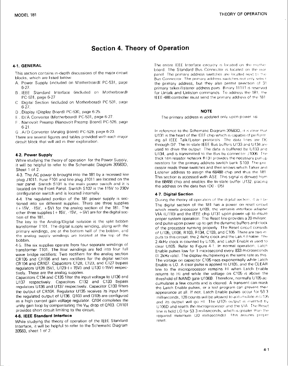
Latch Enable ............................ ~4~2
AID Control Logic .......................
Charge Balance Timing ...................
Single Slope Timing. .....................
Charge Balance-Single Slope Phase
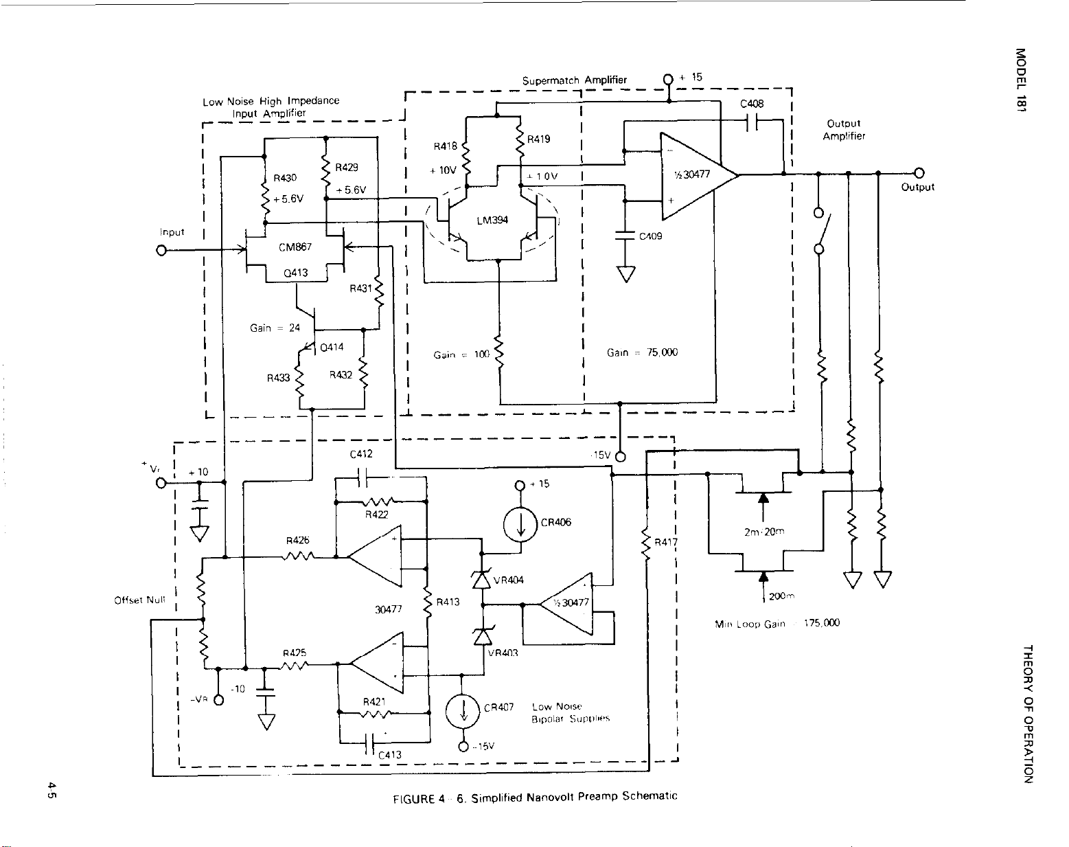
Simplified Nanovolr Preamp Schematic
NVPA Showing Filter Et Drift Correction.
Preamp AID Timing.
V Range A/D Timing
Transconductance Amplifier. ..............
Simplified A/D Diagram .................. 4-10
Integrator ............................... 4~11
Reference Supply ........................
.........
.........
.........
.........
.........
......
.....
......................
......................
PAGE
. . ..l-2
..~.1.2
~2~1
2~1
2~1
2~1
2~1
2-2
~2~2
~3.1
3~2
~4-2
.4~3
~, ,4-3
~4~4
4~5
~4.7
4~8
4-9
,4-9
4-11
5-l
5-2
5-3
5-4
5-5
5-6
5-7
5-8
5-9
5-10
5-11
5-12
5-13
5-14
5-15
5-16
5-17
5-18
5-19
5-20
5-21
5-22
6-l
6-2
6-3
6-4
6-4
6-5
6-6
6-7
6-8
6-8
ShieldedEnclosure..................................................~....~~~
ConnectorAssembly......................................................................~......~.~.~
MaletoMaleConnector
DividerConnection...............................................................................~..~~~~~~.5~ 2
PreampCalibration....................................................~......~.~....~....~~~~~~.~~~~~~~.~ 5.3
DCCalibrator,Kelvin-VarleyDividerandW.. ............... .............
Model1815CalibrationCover..................................................~
480kHzClockl~sec/cm2V/cm..............................~
2.4kHzClock.2~eclcm2Vicm
lnputDisablelOmseclcm2V/cm...................................................................~
lnputDisable50mseclcm2V/cm
ATlOlOutputl0msec/cm2Vlcm..............................................................~
StrobePulsesl0mseclcm2Vlcm..................................................~.......~~~
AT103OutputlOmseclcm2Vlcm...........................................................~..~..~..~~
AT1040utput50msec/cm2Vlcm....................................................................~......5~1 0
V-FOutputl0msec/cm2Vlcm..
lntegratorOutput10mseclcm.5Vlcm.......................................................~........~~..~..5~l 0
AID Output Buffer Output lOOmsec/cm5V/cm
NoisyQ41310pVlcm50ms/cm
Quiet041310~VV/cmWms/cm ......................
NoisyU4O1lOpV/cmWms/cm..
0uietlJ40110~V/cm50ms/cm ...................................................................
Nanwolt Preamp PC-526, Component Location Diagram No. 30377D. Rev. C
Analog Board PC-529, Component Location Diagram No. 30503D. Rev. J
Display Board PC-530, Component Location Diagram No. 30532D, Rev. E
Digital Board PC-531, Component Location Diagram No. 30576D. Rev. J (sheet 1 of 21
Digital Board PC-531, Component Location Diagram No. 30676D. Rev. J (sheet 2 of 21
NanovoltPreampPC-526,SchematicDiagramNo.30586D,Rev.A..
Analog Board PC-529, Schematic Diagram No. 30685D. Rev. C
DisplayBoardPC-530.SchematicDiagramNo.30584D.Rev.C.. ..................
Digital Board PC-531, Schematic Diagram No. 30583D. Rev. F (sheet 1 of 21..
Digital Board PC-531, Schematic Diagram NO. 30583D. Rev F (sheet 2 of 21
............................................................................
..............................................................
......................................................................
..........................
........................... ............. .. .. ..... ..
..............................
..... .......... ....... ..................
...............................
........................... .. .. .......
.............................. ,~, 59
.. ... .. ......
.... ................
.............
... .. ........... .....
................ .. ..... ....
.......................
.......... .. ..
............... ..... ........
.......
............ ~.~,~~~~~ ......... ~5~4
............. ,.,,.~,,~ 5.5
....................... 512
.......... .. .....
.....................
.........
..............
~~,~~
................. ~~~5~10
............... ,.,,5-11
~~,.~
.........
......
.,,,
... ,.~ ,, 5~9
........ ~~~.5~9
....
.... ....
.....
~~,.~ ~,
~~~5~2
..~..~~~5- 2
.. ,5-9
~,
~~~5~10
,5-10
,5-11
5-12
6~15
6~16
...
~6~17
~6.18
~6~19
~6~21
6~23
,6~25
6-27
~6~29
5.2
5-9
5~9
iii
Page 7
I
TABLE
LIST OF TABLES
TITLE
PAGE
Recommended Test Equipment for Performance Verification
3~1
DC Voltage Performance Check (2V to 1OOOVl..
3-2
DC Voltage Performance Check (2mV to 200mVl
3-3
Microcomputer Memory Map ..............................
4~1
Gain Resistors
4~2
Gain Resistors for Volts
4~3
MuxFETs ..................................................
4-4
Recommended Test Equipment ...............................
5~1
Voltage Divider Parts List ................................
5~2
Power Supply Checks .................................
5~3
AIDConverter .....
5-4
Display..
5~5
Preamp Troubleshooting ....................
5-6
DCV Attenuator Troubleshooting
5~7
Replaceable Parts List PC-531 Schematic30593D
Replaceable Parts List PC-529 Schematic30585D
Replaceable Parts List PC-526 Schematic 30586D .........
Replaceable Mechanical Parts ...................
Cross Reference of Manufacturers.
.... ..................
.............. ..
.......................................
.........................................
...........................
~, .. .................
..........................
......
.............. ..
................
..................
.......
~, ...............
........ ......
... .........
.............
...
...
..
.........................
..........................
3-1
.3~1
.3~2
. ...4-2
.4~6
.4~6
. ...4-9
.,.,5-l
. ...5-1
.5-6
.5-7
.5-a
.5~13
.5~13
.6~1
.6~6
.6-10
.6-12
,613
Page 8
I
MODEL 181
Section 1. General Information
l-l. INTRODUCTION,
The Keithley Model 181 is a 5% and 6% digit DC voltmeter
with resolution to lOnV, The Model 181 is a unique DC
voltmeter in the respect that it combines microprocessor
technology for full programmability with a new concept in
nanovolt front ends, It provides highly accurate, stable and
low noise readings from 1OnV to 1CCQVDC on 7 voltage
ranges. The 2V through the 1CCOV ranges utilize the 5.way
binding posts. The 2mV through the 2CQmV ranges utilize the
special low thermal input connector.
The service manual contains the necessary information for
calibrating and maintaining the Model 181. This information is
provided in various sections throughout the manual. These
sections are listed as Performance Verification, Theory of
Operation and Maintenance/Calibration. Along with this
section, General Information, this manual also includes the
Accessories, a Parts List, and the Schematic Diagrams,
GENERAL INFORMATION
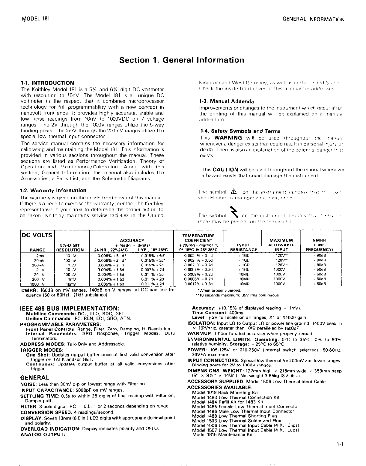
CMRR: 16OdS on mV ranqes. 140dS an V ranges; at DC and line fre
quency 60 or 60Hrl. ,lkR unbalance)
IEEE-488 BUS IMPLEMENTATION:
Multiline Commands: LXX. LLO. SDC. GET.
Unlline Commands: IFC, REN, EOI, SRD. ATN.
PROGRAMMASLE PARAMETERS:
Front Panel Controls: Range. Filter. Zero, Dampin% Hi Resolution.
Internal Parsmeters: SRCI Resoonse. Triswsr Modes. oats
Tetminators.
ADDRESS MODES: Talk-Only and Addressable.
TRIGGER MODES:
one Shot: Updates OUtpUt buffer once at first valid c”““ersi”” after
tdocler on TALK and/or GET.
GENERAL
NOISE: Less than 30nV pip on lowest range with Filter on.
INPVT CAPACITANCE: 5OOOpF on mV ranges.
SETTLING TIME: 0.5s to within 25 digits 01 final reading with Filter on,
Damping off
FILTER: 3~pole diSital: RC = 0.5, 1 or 2 seconds depending 0” range.
CONVERSION SPEED: 4 readings/second.
DISPLAY: Seven 13mm (0.6 in.1 LEO digitswith appropriatedecimal point
and polarity.
OVERLOAD INDICATION: Display indicates polarity and OFLO.
ANALOG OUTPUT:
--
Accuracy: f 10.15% of displayed reading + lm”i~
The Constent: 400ms.
Level: t 2V full scale on all ranges: x1 or x,000 gain
ISOLATION: Input LO 10 Outpur LO or power line ground’ ,400” peak. 5
x lOW.Hz. greater than ,090 paralleled by ,soJ”F
WARMUP: 1 hour IO rated SCCUE.CY when propedy zeroed,
ENWRONMENTAL LIMITS: OperatinS: WC 10 35°C. 0% la 80%
re,atiw hwnidirf .storags: 2vc to 65°C~
POWER: 105~125V or 210-250” lintelm SWlWh selected,. 50~60HZ.
30V.A maxim”m.
INPUT CONNECTORS: Special low thermal to, 20OmV and lower ,ilnges
Binding posts f”,2V to tooov rangss.
DIMENSIONS. WEIGHT: 127mm high x 216mm wde I 359mm deep
15” x BK” x 14W’,. Net weight 3.85kg ,8K lb*.,,
ACCESSORY SVPPLIED: Model ,606 Low Thermal Input Cable
ACCESSORIES AVAILABLE:
Model 1019 Rack Mounting Kit
Model ,483 LOW Thermal Connectlo” Kl,
Model 1484 Refill Kit for 1483 Kit
Model 1485 Female LOW Thermal Input Conneclor
Model ,486 Male LOW Thermal Input Connector
MO& 1488 LOW Thermal Shorting Plug
Model 1503 LOW Thermal Solder and Flux
Model ,506 LOW Thermal Input Cable 14 1tL alps,
Model ,507 LOW Thermal Input Cable 14 11.. Lugs1
Model ,815 Maintenance Kit
Page 9
I
I
GENERAL INFORMATION
NOTES
1~ NMRA spocilicalions applies for input signals less than 3. ZEROING
12OmV peak~to~peak on the 2mV and 20mV range, ,.2V
poak~to peak on the 200mV range and less than 2X fuli
scale peak~lo-peak on all other ranges. This is necessary in
ordci 10 prevent AID sauration
2 ACCURACY SPECIFICATION
The accuracy specifications arc defined exclusive of noise
The term “when properly roroed” means rereroing during
warmup ifIrs 4 hoursi and after ambient changes in
temperalure of greater than 1’C
MODEL 181
l-2
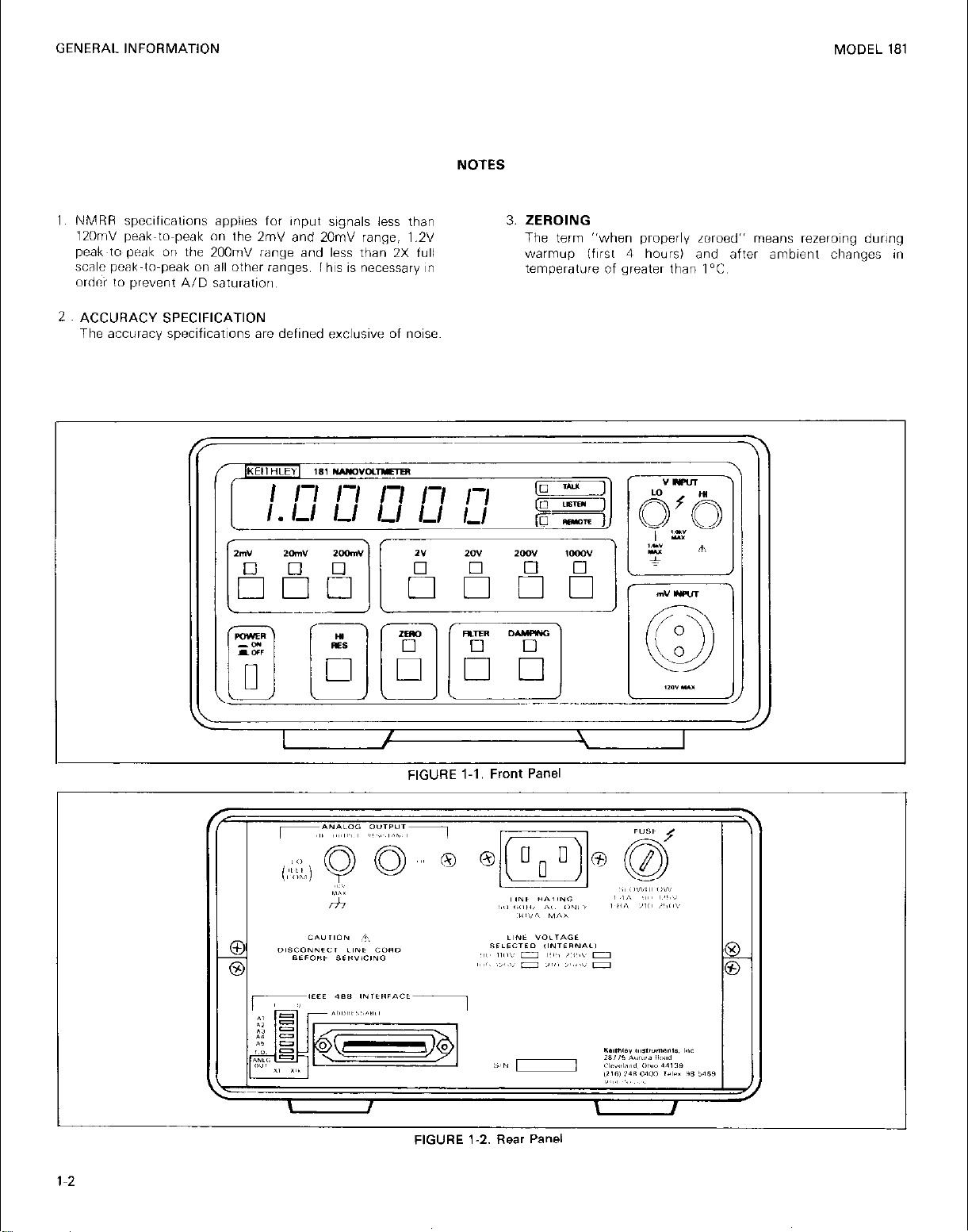
F,G”RE l-l Front Panel
FIGURE 1-2. Rear Panel
Page 10
MODEL 181
Section 2. Accessories
2-l. GENERAL
This section describes rhr? va,ious xcesso,~~~s and options
available lor us” with the Model 181.
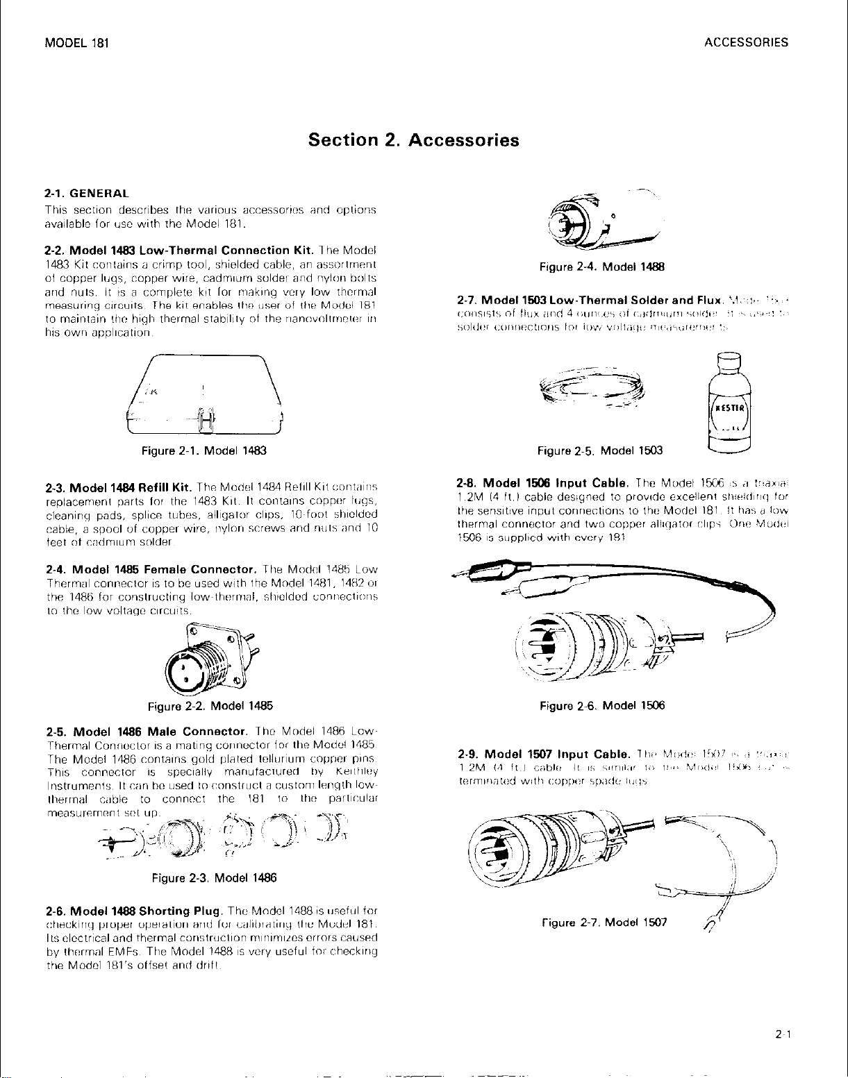
2.2. Model 1483 Low-Thermal Connection Kit. 1 he Model
1483 Kit Conlains a crimp tool, shielded cable, an assortment
01 copper lugs, copper wire, cadm,um solde, and nylriri brrlts
and nuts, i, is a com,,le,e kit lo, nrnk,ng v”,y low thcrmnl
measuring arcuifs, ihe kit enables th,! use, of ,118 Mode1 181
10 maintain ho i~iqh therma stability 01 the ,~anov,~ll,,m~l,?~ II!
t11s own appllcatiorl,
Figure 2-l. Model 1487
Figure 2-2. Model 1485
Figure 2-5. Model 1503
Figure 2-6. Model 1506
Figure 2-3. Model 1486
2.5. Model 1488 Shorting Plug. ~T~hr! Model 1488 is ~,sef~il for
checking proper operation and Ior cnlihratinq the Model 181~
Its electrical and thermal ~0,1stri~l10,1 mrlimms “,,“,s caused
by thr!,mn, EMFs, The Mode, 1488 is ““,y useful fm checkirii?
the Model 181’s offset and drtfl~
Figure 2~7. Model 1507
4
Page 11
ACCESSORIES
‘\
.-.
,.
‘:. 3.
MODEL 181
7
;:‘r
Figure 2.8. Model 1815
Figure 2-9. Model 1019
2-2
Page 12
MODEL 181
PERFORMANCE VERIFICATION
Section 3. Performance Verification
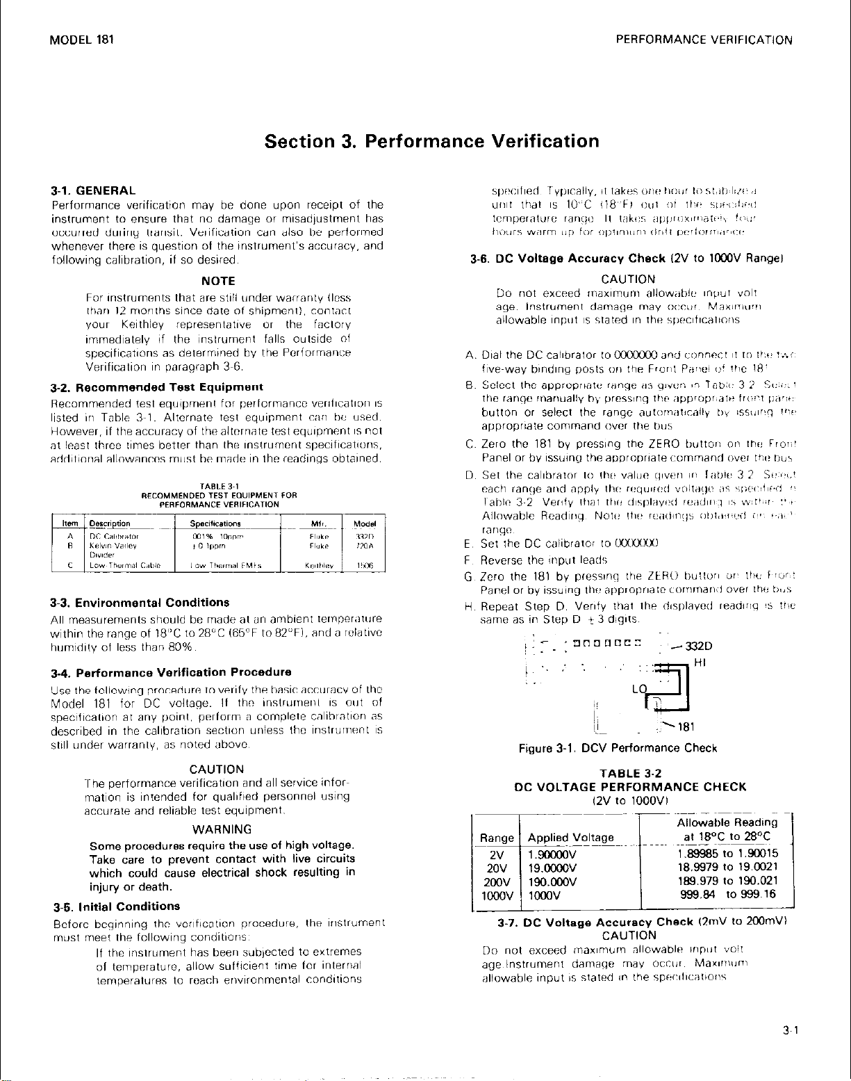
3-6. DC Voltage Accuracy Check i2V to 1wOV Range1
3-4. Performance Verification Procedure
Use the following procedure 10 verify fhe basic accuraw of the
Model 181 ior DC voltage. /I the instrumwIl IS out of
speciflcallon ar any point. perform a complete caIib,atiori iis
CAUTION
The performance verification and all service inform
mation is intended for quaIlfled personnel using
accurate and reliable test eqwment.
WARNING
Some procedures require the use of high voltage.
Take care to prevent contact with live circuits
which could cause electrical shock resulting in
injury or death.
3.5. Initial Conditions
Before beginning thu ver,f,ca,ion procedure. the ,i,slrument
must meer the followng conditiorls:
l, the instrument has beer, subjected 1” extremes
ol temperature, allow sufficient fime for interrlal
kmperatures 10 reach wwronmental conditions
1 ‘. : :
(I
Figure 3-l. DCV Performance Check
DC VOLTAGE PERFORMANCE CHECK
I
I
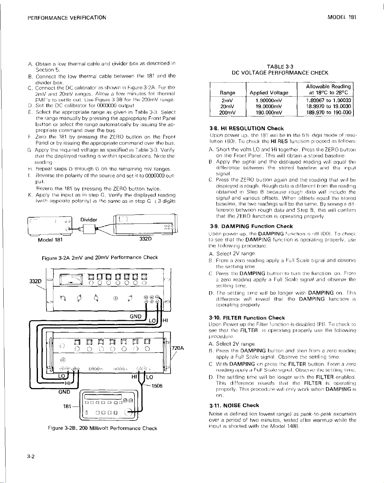
3-7. DC Voltage Accuracy Check l2mV to 200mVl
TABLE 3-2
12v to 1OOOVl
CAUTION
.,‘181
1.89985 to 1.90015
,6.9978 to 19.0021
,E!xs,s 10 190.021
999.84 to999.16
Page 13
I
PERFORMANCE VERIFICATION
MODEL 181
A. Dbtnin a low thermal cable and divider box as described in
Section 5.
B. connect the low thermal cable between the 181 and the
divider box.
c. Connect the DC calibrator as shown ill Figure 3~2A. For the
ZmV md 20mV rangm Allow n few nlinUk?S for fhc!rrnal
FMF’S to settle OUL~ Use Figure 3~38 for the 200mV range.
Do Set the DC calibrator for OOWOOO output
E. Sclnct the appropriate range as given in Table 3-3 Select
the range manually by pressing the appropriate Front Panel
button 01~ select the range automat~caily by issuing the apt
propriate command over the bus.
F, Zero the 181 by pressir,g the ZERO button on the Front
Panel or by issuing the appropriate command over the bus.
G Apply lhe riiquired voltage as specified in Table 3~3. Verity
that the displayed reading IS wllllin speclficalions~ Note the
X!X,lM]~
Hi Repeat steps D through G on ,he remaining mV ranges,
I, Reverse the polarity of the source and set i, t” 0000000 a,,~
p”l~
Rerero the 181 by pressing the ZERO button twice.
K. Apply the input as in step G. Verify rhr displayed rcadfng
iwIth opposite polarityi is the same as in step G +3 digits
no
,Y n
Made, 181
Figure 3.2A 2mV and 20mV Performance Check
TABLE 3-3
DC VOLTAGE PERFORMANCE CHECK
3.8. HI RESOLUTION Check
LJpon power [up, ftlc 181 WIII ba in the 5% dlgiI mode ol l~eso~
lllfion iROl~ To cheek fho HI RES funcl~on prncood as follows,
A~ Short thevolts IL0 2nd HI togrthcr~ Press the ZERO butlor~,
on the Front Panel. ~lhis will obtain a stored bascline~
I3 Apply the signal and the displayed reading will cqual thn
dilfr.rence between the stored baseline and the ,npu,
SIgnal.
3-9. DAMPING Function Check
Upor power up, the DAMPING fur,i:t,r,n IS r,,f iDO,, To check
10 see Ihat thi! DAMPING function IS operal~n!] properly, use
me l”llnwlilg procrd”,~e:
A. Select 2v ranq3
8. From a zero reading ;rprily a Fuil Scale signal and obserw
the serrling time,
3-2
I I I I
Figure 3-28. 203 Millivolt Petiormance Check
3-10. FILTER Function Check
Upon Power up the Filter functfon is dfsabled IPlI To chock to
see Li?at the FILTER IS operatfrq properly ust? Ihe following
procedure
A. Select 2V range.
/
H. Press the DAMPING burtor, and ti,w from a 7810 roedln~~
apply R Full Scale signnl Dbscrve fhc settling time,
C With DAMPING on press Ihc FILTER button Frorr a irro
rradli,rg apply a Full Scalii signsl~ Obswvc tl,e sctllmg l,mr.
Do The settling Lyme will be lorrger with thr FILTER enablcti
1 IliS dlffercnce ic”Cals ,ili,l the FILTER is operating
properly. Ths proccdur~ will wily work whcr DAMPING is
“11~
3.1,. NOISE Check
Noise is detined Ion lowest range, as peak-wpeak excursion
over a period of two minutes, tested after warmup while the
inpul is shorted with the Model 1488
Page 14
I
MODEL 181
Procedure for checking notse:
A. Short the mv ,npu, w,,h a Model ,488 Low Thermiil Short
B. Select the 2mV range,
C. Turn on HI RES so that 6’% digits arc displayed.
PERFORMANCE VERIFICATION
Page 15

Page 16
MODEL 181
Section 4. Theory of Operation
4-l. GENERAL
This section contains ln~depth discussions of the maj”r circuit
blocks, which are listed below:
A. Power Supply (included on MotherboardI PC~531. page
B IEEE Standard lnrerface iinr:ludcd on MotherboardI
PC ~531, page 6~27
C DigItal Section (included on Mofhcrboradi PC~531. page
D Dispiay [Display Board1 PC~530, page 6,25.
E D/A Converter iMotherboard PC~531. page
F Nanovolt Preamp lNanovol~ Preamp Board1 PC~526. page
G A/D Corrvcrter (Analog Board) PC~529, page 6~23,
There are several figures and tables [provided wilt1 each major
circuit block that will aid in their oxplanation~
6~27,
THEORY OF OPERATION
4-z. Power supply
While studying the theory of operation for the Power Supply.
it will be helpful 1” refer t” the Schematic Diagram 30583D.
Sheet 1 of 2.
4-3.
The AC power is brought int” the 161 by a recessed line
plug JlOll. Fuse FlOl and line plug J,O,l are located on the
rear panels Switch SlOl is the main power swtch and ii is
located on the Front Panel. Switch S102 is the 115V 1” 230V
configuration switch and is located internally.
4~4
The regulated portion of the 181 power supply is sect
tioned into six different supplies. There are three supplies
(+15V, -15V, +5V) ior the analog section of the 181. The
other three supplies (+ 1%‘. -15V. -+ 5VI are for the digital section of the 181.
The key to the Analog/Digital isolation is the split bobbin
transformer TlOl. The digital supply winding, along with tbe
primary windings, are at the bottom haIf of th~ bobbin, and
the analog supply windings am located al the lw of the
bobbin.
4~5. The six supplies “perate from four separate windings 01
transformer TlOl. The four windings are fed info four full
wave bridae rectifiers: Two recfifiers for the analog section
CR105 ani CR106 and two rectifiers for the digital sect~“n
CR104 and CR107. Capacitors C128, C123. and Cl27 bypass
regulators U12B l5VI, U129 (+ 15Vl and U130 I-15Vl respectively. These are the analog supplies.
Capacitors Cl34 and Cl35 filter the input voltage to U136 and
U137 respectively. Capacitors Cl32 and Cl33 bypass
regulators U136 and Ul37 respectively. Capacitor Cl30 filters
the “utput of CRlC4 Regulator U135 receives its input from
the regulated “utput of Ul36. Q103 and Q105 are configured
as a high current gain voltage regulator. 0104 completes the
unify gain loop by compensating the VeE drop of Q103. CR101
provides short circuit limiting t” the circuit.
4-6. IEEE Standard Interface
While studying the theory of operation oi the IEEE Standard
Interface, it will be helpful 1” refer to the Schematic Diagram
30583,
sheet 1 of 2.
Page 17
I
THEORY OF OPERATION
X5B30, Sheet 2 of 2 and 305&D, The digital cont~9 civails
of the 181 AID are located on Schematic 30583D. Sheet 2 of 2
while the circuits that they control are located on Schematic
30585D.
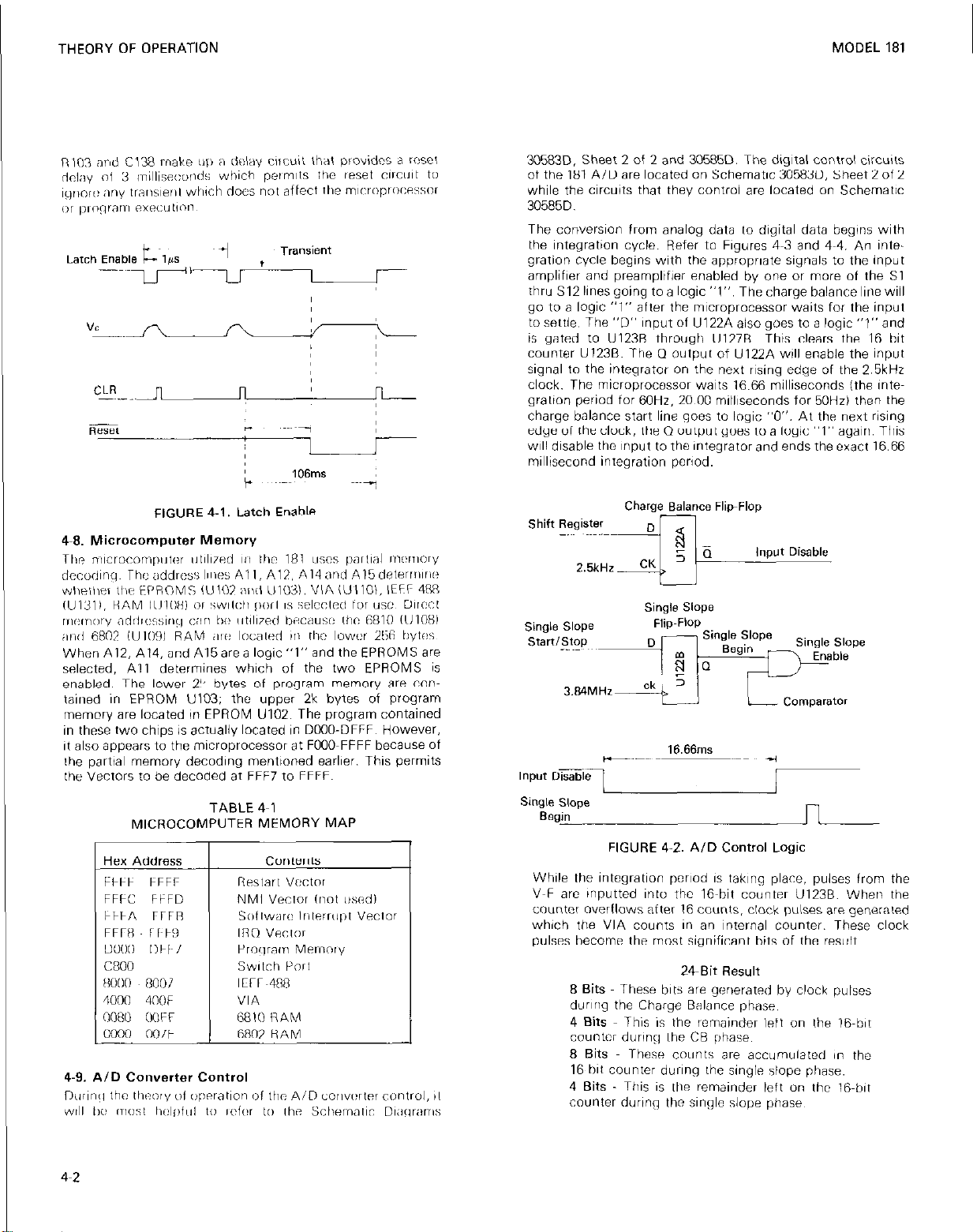
The conversion from analog data 10 digital data begins with
the integration cycle. Refer to Figures 4~3 and 4~4. An integration cycle begins with the appropriate signals to the input
amplifier and preamplifier enabled by one 01 more of the Sl
thru S12 lines going to a logic “1”. The charge balance line will
go to a logic “1” after the microprocessor waits for the input
to settle. The “D” Input of U122A also goes to a logic “1” and
is gated 10 U123B through U127B. This clears the 16 bit
counter U123B. The Q output of U122A will enable the input
signal to the integrator on the next rising edge of the 2.5kHr
clock. The microprocessor waits 16.66 milliseconds (the in&
gralion period lor 60Hr. 20~00 miillseconds for 60HrI then the
charge balance start line goes 10 logic “0”. At the next rising
edge of the clock, the Q output goes to a logic “1” again. This
WIII disable thn Input to the integrator and ends the exact 16,66
millisecond integration period.
Charge Balance Flip-Flop
MODEL 181
4-2
TABLE 4-l
MICROCOMPUTER MEMORY MAP
FIGURE 4.2. AID Control Logic
While the integration pcrlod is taking place, pulses from the
V~F arc inputted into the l&bit counter U123B. When the
co”“tcr overflows after 16 cowts, clock pulses are genoiared
which the VIA counts in an internal counter. These clock
pulses become the most significant bits of the result.
24-Bit Result
8 Bits These bits are generated by clock puises
during the Charge Balance phase.
4 Bits This is llhe remainder left on Ihn l&bit
cou”lcr durinij ,he CB phase.
8 Bits These counts are accumulated in the
16 bii counter during the single slope phase.
4 Bits This is Ihe remainder left on the 16~bir
counter during the sin(~lc slope phase,
Page 18
MODEL 181
Strobt- /
u
j --mllJlJr
E”df”z ~ /y Remainder Strobe P”‘ses
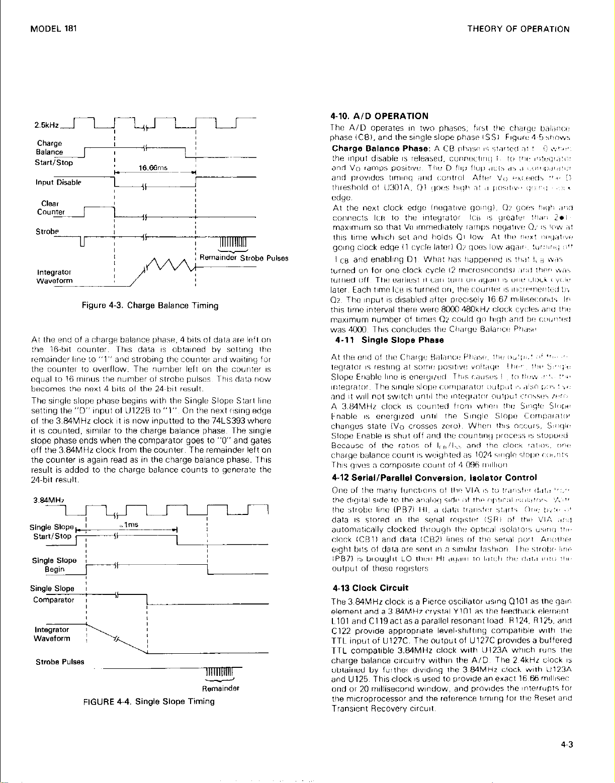
Figure 4-3. Charge Balance Timing
THEORY OF OPERATION
The single slope phase begins uwth the Single Slope Start l~“e
setting the “D” input of U122B 10 “l”, 0” the next risirlg edge
of the 3.84MHr clock it is “OW inputted fo the 74LS393 where
if is counted, similar to the charge balance phases The single
slope phase ends when the comparator goes to “0” and gates
off the 3.84MHr clock from the confer. The remainder left on
the counfer is again read as in the charge balance phase. This
result is added to the charge balance cwnfs fo generate the
24~bit result.
Single Slope, !
start/stop
Single slops ,
Begi”
,,-lrnS-
r
I
FIGURE 4-4. Single Slope Timing
Page 19
I
THEORY OF OPERATION
Input Disable
TO countet
0
MODEL 181
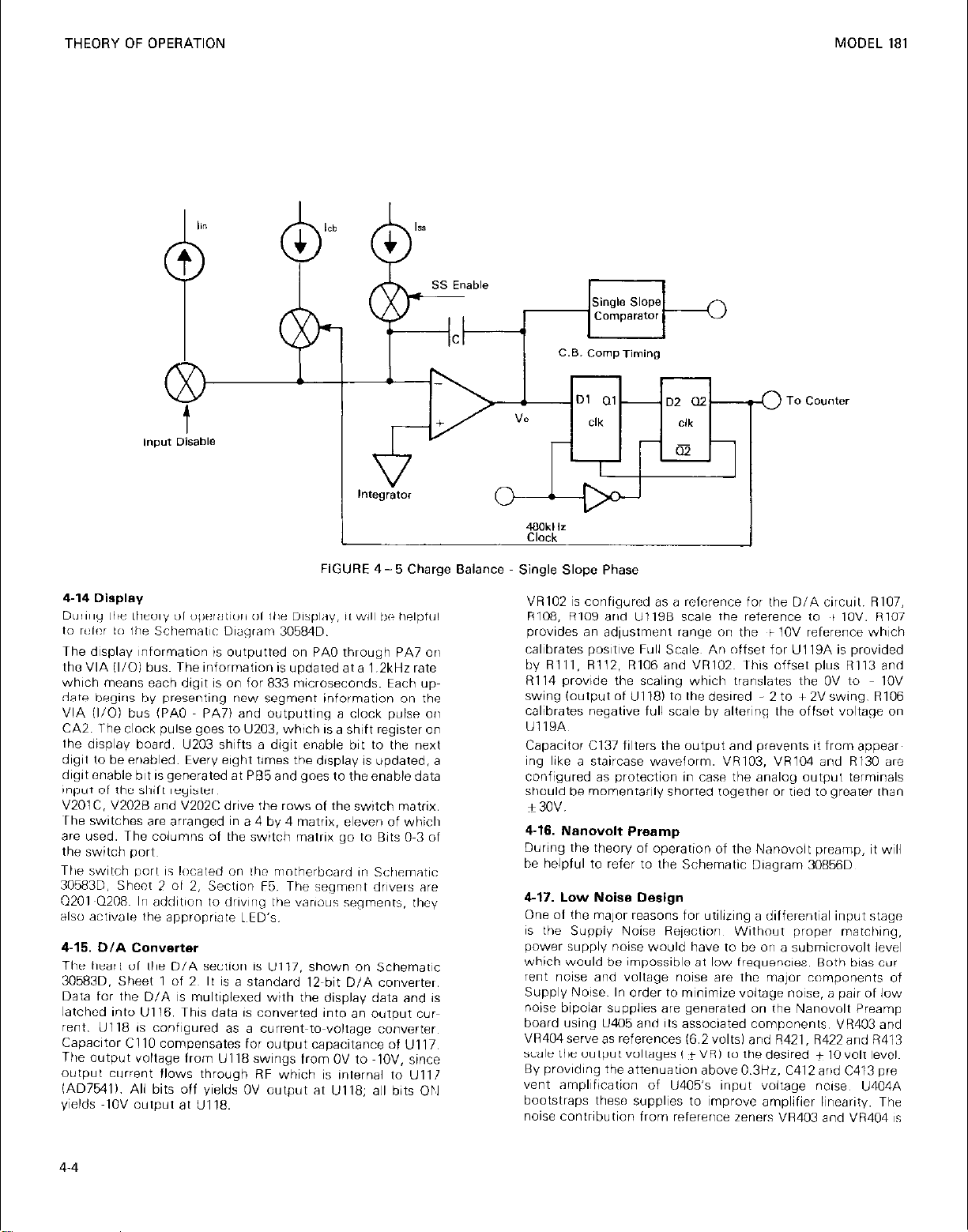
FIGURE 4-5 Charge Balance Single Slope Phase
4-14 Display
The display lr,formation is outputted on PA0 through PA7 on
the VIA II/O1 bus. The information is updated at a 1.2kHr rate
which means each digit is on for 833 microseconds. Each update begins by presenting new segment information on the
VIA II/O1 bus (PA0 PA71 and outputting a clock pulse oil
CAZ. The clock pulse goes to U203, which is a shift register on
the display board. U203 shifts a digit enable bit 10 the next
digit to be enabled. Ever” eiqht times the displav is updated. a
digitenable bit isgeneratedat P85andgoesto theenabledata
input of the shift register,
V201 C. V2028 and V202C drive the rows of the switch matrix.
~The switches are arranged in a 4 by 4 matrix, eleven of which
are used. The columns of the switch matrix go to Bits O-3 of
the switch ports
The switch port IS located on the motherboard fn Schematic
30583D. Sheet 2 01 2, Sectlo” F5. The segment dwers are
0201 0208~ 111 additlor to driwng the various segments, they
also artivak Ihe appropriale LCD’s,
4-15. DIA Converter
The heart of the D/A section is U117, shown on Schematic
30583D. Sheet 1 of 2~ It is a standard 12~bit D/A converter.
Data for the D/A IS multiplexed with the display data and is
latched info U116. This data is converted into an output current. Ul18 IS configured as a current-to~voltage converter.
Capacitor Cl10 compensates for output capacitance of Ull7.
The output voltage from U118 swings from OV to -1OV. since
ouiput current flows through RF which is internai to Ulll
lAD75411. All bits off yields OV output at Ull8; all bits ON
yields ~IOV output at Ul18.
VR102 is configured as a rcfcrence for Ihe D/A circuil. RIO/,
R108, RI09 arrd U119B scale the reference to ! 1OV. R107
provides an adjustment range on the + 1OV reference which
calibrates positive Full Scale An offset for U119A is provided
by Rlll, R112, R106 and VR102. This offset plus R113 and
R114 provide the scaling which translates the OV to 1OV
swing loutput of U1181 to Ihe desired 2 to +~ 2V swing. R106
calibrates negative full scale by altering the offset voltage on
UllSA,
Capacitor Cl37 filters the output and prevents it from appear
ing like a staircase waveform. VRlO3, VRIO4 and RI30 arc
configured as protection in case the analog output terminals
should be momentarily shorted together or tied to groater lhan
+3ov.
4-16. Nanovolt Presmp
During the theory of operation of the Nanovolt preamp, it will
be helpful to refer to the Schematic Diagram 30856D
4.17. Low Noise Design
One of the major reasons for utilizing a differential input stage
is the Supply Noise Reiec~ion Without proper matching,
power supply noise would have to be or a submicrovolt level
which would be impossible at low frequencies, Both bias cur
rent nom and voltage noise arc the major components of
Supply Noise. In order to minimize voltage noise, a pair of low
noise bipolar supplies are generated on the Nanovolt Preamp
board using U405 and IIS associated componen& VR403 and
VR404 serve as references (6.2 volts1 and R421, R422 and R413
scale the outpur voltages / ~+VRI 10 the desired f lOvolt Ievcl~
By providing the attenuation above 0.3Hr. C412 and C413 pre
vent ampllficafion of U405’s input voltage news U404A
bootstraps these supplies to improve amplifier linearity. The
noise conirlbution from reference zeners VR403 and VA404 IS
4-4
Page 20
I I
+vr ’
0
N”li
, +I0
/;5
I
I
I
I
I
I
I
I
-va
I
I
I
I
--
~10
b ‘s
---
----
_----
--------
)
-
-----
Page 21
THEORY OF OPERATION
MODEL 181
rnugl~yiblo, The bootstrap supply is decoupled from the input
via C414. C415, R425and R426. Rejection from the + 15V sups
plies is critic;iil as well. Therefore. current regulators CR406
and CR407 are a necessity iRp> 1M ohm) since Rs of VR403
and VR404 is approximately 100 ohms,
The key to maintaimng low current noise in the drain circuit of
Cl413 IS the selection of a low noise, high gain device for Q414
and maintaining low emitter and base impedances over the
bandwidth, R431, R432 and R433 provide bias for Q414 and
are referer~:ed 10 _t VR for low noise contribution
Noise contribution from the second stage depends upon drain
loads of Q413, gain of the lirst stage and input noise of the second
srage~ Q412 is a precisely matched low noise amplifier Wan
sister piiir which act as the second stage for the 181 preamp,
III addilior 10 low now, Ihls fransislor pa~r IQ4121 is required
because of 1,s hlgtl CMRR performance.
4.18. Linearity and Gain
,r a diifarential DC amplifier. nonlinearities irI the input stage
provide Ihe Iirnifal,on 10 gain linearity under the closed loop
condluon. In fact, no amount of loop gain car cailcol these
nonIinearities. The input FETS are square law devices which
means the output current varies as the square of the VGS. In
order fo r:anr:o, this nonlinearity. a second FET is used as a
load 10 the Hurst FET idifierer,lIaI pair). The degree of linearity
depends upon the match,ng between the two devlces~
The lolaI amplifier loop gain must be kept high so that closed
Ioop gain is independent of open loop gain. This eliminates
problems with gain drifts due to time/temperature var~atlons
inside Ihe loop. To maintain stable closed loop gains of 1000
i2mV rangel. 100 IZOmV range1 and 10 (200mV range) apt
propriate film or wirewound resistors are chosen as feedback
elements. Refer to Table 4~2~
TABLE 4-2
GAIN RESlSTORS
Range
2mv R40S. R414. R435 1000
ZOnl” R410, R415, R435 10” R410
zoomv R411, R416. R434
Thermal drifts in the input amplifier are relatively unimporfant
since they are autozeroed our. Slowly varying drill come
ponents isuch as solder joints, reed relay contacts) are of little
significance. ‘Therefore, no special lowthermal term~naIs are
necessary irl the feedback ,oop
However, for the nanovolt ranges (2mV. ZOmVl, it IS
necessary Lo use wirewound resistors wherever low voltage
signals are present, This is why R435 is a wirewound element,
whereas R434, R409-R416 are film resistors. Film resistors
display much higher voltage noise whereas wirewounds are
avaiInb,e whose noise approaches theoretical limifs. R435 is
s&x&d as 200 ohms since the Johnson noise of this value is
negligible compared to amplifier noise.
Gain Resistors Gain Adjustment
R40S
10 R411
4.20. Offset Null
4.21. NMRR Filter and Buffer
Additional NMRR is provided 111 the preamp using a threepole
cascaded filter. As can be seen from Figure 4~7. the three
poles are provided by three RC networks~
Wher, FFT Q4,S turns o,. sii drw 0405. 0407 and Q4OS~ The
fliters arc mow in tile nrw11 arrd Ihe input signal is now liltered
and amplliicd, The filter settling I~me is equal 10 200
mi,Iiseconds. After lhe 200 millisecond ~rlferval the signa
integration 1s done by the A/D~ FET 0420 (now lums 011, and
FETs Q419. Q405, Q407 arid 0408 lurn off, Since 110 liller IS !n
while the amplifier looks at “zero,” settling time depends on
amplifier speed and is 4 milliseconds. The zero is lhen Inn
tegrated by the A/D.
The reasorl the filter must shut off is so fhc A/D can record
amplifier xxo rlghl after if records sign;lI By keeping the tlrll~
delay bctween signal anti iclo as small as pilss~t~lo, effective
,,o,se ar,d dr,f, iire reduced tc lI,e desired lkwel. Co~lcurrerltly,
filtering of ~nrxmal mode signals IS accomplished only whet1
needed; wl,an looking at the signn,~
T11e first pole is formed by “416, C407 and Q4oS. The on
resistance of Q409 rnair~lains i:,osed loop gain aI all ire
qurncies greater than 10 which maintains ampI,firr stability~
The second pole is formed by C406. R406 and Q407. It is butt
fered from tile third pole by U401 5, The third pale is formed by
R401, C403 arid Q405~ AI, 11,rw ,x>Ies ,havr Ihr same 1,mc con
slant 01 10 miI,lseconds~ U401A builcrs Ihr: oulput 01 thn third
p0le.
Buffers U4OlA and U4OlB are boo&trapped in a similar
fashion to the input amplifier. VR401 and VR402 provide the
+6.2V reference, and emitter followers WI1 and Q402 supply
Ihe currenl 10 ,,4Ol, R40,C and R407D b,as Ihi! r~iemnces.
The effect oi This boofstrap is fo provide higher CMRR 10
“401, Ihnrefore imprrivirng linearity.
The baotstia,, CllClllt aoiis a pole I” 11k ir”qlicrrcy rcsp”“sa 0,
U4016. The dominant pole formed by R407A. R407R. C401
arid C402 m~intnins stability rif the bootsrrap c~rcoif. Q403 and
Q404 illIi ,ciw capai:ilarK:~
boolslraji c~rcuil to preve~lf latch up rcsult,ng lrom driviing
inputs to U4OlB out 01 lhoir common mode range durincj
overload
FtTs used as d,odc clamps 10 Ihii
4-6
Page 22

I
MODEL 181
FIGURE 4-7. NVPA Showing Filter and Drift Correction
THEORY OF OPERATION
4-22 Drift Correction
The offset resistors A423 and R424 bring the amplifier ~ni” the!
operating rang”. The “f&et can only be nulled 1” 2m” referred
to the input. At the output on X1000. 2V can be presents The
AID would be overloaded by i:2,4V which means the 2V
component must be offset t” 0” for OV,“,
This offset c”rrec,,“n IS pr”v,ded by C404. 0406 and low
leakage buffer U4OlE. When Q420 IS on and when th” A/D IS
not lookIng at preamp zer” (during the A/D zero cycle1 Cl406
turns on and stores the offset voltage present on the DC
amplifier output “n C404. Then this capacitor holds this value
during the next two conversions 1.5 secj until it 1s updated.
This correction occurs two hmes a second. Leakage off this
capac~toi will yield offsets on the 200 m,lliv”l, range wiih ,nput
shorted. The major swrce of leakage is U4OlB and 0406.
These two devices are selected for leakage to mantain less
than 15 microvolls of drift over a conversion cycle of 50
millisecond. This is the time it takes 1” do a full preamp
signal/zero conversion. C405 prevents preamp slewing ibet~
ween signal and zero FET switching) from affecting the charge
on c404
4-23 Input Protection
CR402 and CR403 prevent input stage foldover which would
severely drop input impedance during overload. This also
prevents long recovery time caused by unbalancing power
dissipation between Q413A and 04138. 0410 and Q411 prevent the amplifier from getting lost during a range change or
severe overload by clamping the summing junction at * 1V.
CR&J, CR405, R427 and R428 provide a ground referenced
f0.7V threshold for the protection circuitry. High impedance
( ) 10Q ohm1 is not affected by the protection circuit for input
voltages less than 1 volt because of low leakage FET pair Q415
and 0416. However, for inputs greater than 1 volt. the input
““Itage is clamped and current limit is provided through R436.
Page 23

THEORY OF OPERATION
GAIN RESISTORS FOR VOLTS
MODEL 181
TABLE 4-3
4-E
1
LrKLr
FIGURE 4-8. Preamp A/D Timing
Page 24

I
MODEL 181
ON
Signal
S-line
OFF
Input Disable
WE_
mnsec
.4
1
THEORY OF OPERATION
OurrIm”
ON
ON
OFF s3
ON
OFF s4
,ntegrate
Rd FET
AID Zero
FET
16.66rnsec
.,, - -4rnSBC
A” I
FIGURE 4-9. V ran@ A/D TimIn
TABLE 4-4
MUX FETs
l-l-rLr
I--.-~-
~C e 4msec
4-B. MUX FETs
h
F~GVRE 4 - Il. Transconductance Amplifier
Page 25

Input Buffer
Single Slope
Comparator
Comparata
Output
+
4.7K
a
&kHz
Clock
IllpUt
ml/O Lines From pC.
FIGURE 4- 10. Simplified A/D Diagram
Page 26

MODEL 181
4.31. Integrator
The integrator has been designed to guard against the most
common problems associated witil tligh speed ~nlagrator
operation. Active integrators have two major problems which
limit their high speed performance: the cro~~ovei dtstortion
and the gain bandwidth of the integrator amplifier, These effects can be seen by looking at the integrator model in Figure
4-12. When a voltage step appears at Vin, the amplifier will not
respond immediately and C will initially be a short circuit
Then:
as shown in the nquat~on, the effect is that the wrong current
will be applied to the capacitor until the amplilier recovers~ /I
can also be seen that I/ a hipolar input amplifier was used for
the integrator, charge could be conducted away from Ihe
capacitor and cause significant erron To guard against these
problems, the 181 uses a bias resistor on the integrator output
to 15V to keep Ro small into the MHz region, and ail inputs
to the integrator are current sources. A FET input op amp IS
used which allows a few volts to appear on the summing junc~
tion with no loss in charge.
c
Ri”
-
THEORY OF OPERATION
R3x + R332
6-
FIGURE 4-13. Reference Supply
FIGURE 4- 12. Integrator
Page 27

Page 28

I
MODEL 181
MAINTENANCE
Section 5. Maintenance
5-l. GENERAL
This section contains information necessary to maintain the
Model 181. Adjustment/Calibration, troubleshooting and fuse
replacement procedures are provided. Calibration should be
performed yearly (every 12 months) or whenever 24 hour
specifications are desired or whenever performance verifi~
cation isee Section 3) indicates that lhe Model 181 is out of
specifications. If any step in the calibration procedure cannot
be performed properly, refer to the troubleshooting inform
mation in this section or contact your Keithley representative.
or the factory.
NOTE
Because of special handling, expertise, and
equipment that is required. it is strongly recom
mended that the 181 be sent back to the factory
for service andlor calibration.
WARNING
All service information is intended for qualified electronic maintenance
5-2. Recommended Test Equipment
Recommended test equipment for calibration is listed in Table
5-l. Alternate test equipment may be used. However, the
accuracy of the alternate test equipment must be at least three
times better than the Model 181 specifications, or equal to
Table 5-l specifications.
5-3. Voltage Divider
The Voltage Divider IBI recommended is not readily available
on the commercial market. The following information IS prop
vided in order that this divider may be constructed.
persOnnel
only.
VOLTAGE DIVIDER PARTS LIST
Keithley
Part Number
BP-l,-0
BP~ll-1
Model 1485
N/A
N/A
Model 1483
C. 2WA-29 Washer
D, 1 19166 Strain relief
I Black Blndlnq PO51
Red B,nd,ng Post
LowThermal Female Input
lIXlk0. 01%. 10ppmi”C. Wirewounil
Low Thermal Construction
lC0R. .Ol%, 10ppml°C. W~rewourrd
Low Thermal Construction
Low Thermal Construction KI,
TABLE 5-2
Description
Connecter
Item A Description
DC Calibrator
Voltage Divider
Oscilloscope
DMM
Maintenance Kit
Kelvin Varley Divider
Law Thermal input
Cable
Low Noise
Preamplifier
RECOMMENDED TEST EQUIPMENT
TABLE 5-l
Specifications
1.9v. ISV, 19ov. loco/
+ .ool% ,10ppmi
+ .Ol% IlOppml
2mClcm
.003% + Id
Mfr. Model
Fluke
332D
7603
5903
1815
720A
1481
Page 29

MAINTENANCE
FIGURE 5-l. Shielded Enclosure
MODEL 181
Pin El
Pin A
To prepare a low noise triaxlal cable for either d~recl cow
nr~tioris to a source or lor connector assembly Ihc stops
outl~nrd below should bc followed,
A. Gently c”t through the o”ter insulation without
cutting the oukr shield
B, Using a sharp point, unravel the braided shield,
C Twist Ihe bt~aid /o”tcr shield) and thoroughly clear off
traces of graphtte.
Do Gently cuI through the inner insulation without
cutting the inner shleld~
t. Using a sharp point, ~“nraw? Ihn braided shield.
F, Twist the braid
iinner
shield) and thoroughly clean off illI
traces of graphite.
Go Cut the center conductor to the proper length and strip
the insulation off of the center conductor,
H. Refer to Ftyure 5-2 and crimp the center conductor to Pin
A Crimp the inner shield 10 Pin B. Place the outer shfcld
braid between the two washers and secure the back of
the coni,ector as showrn
FIGURE 5-3. Male to Male Connectol
Heier 10 Figure 54 for a cornplate picture of lhe Calibrator to
Voltage Diwder lo 181 Connection.
5-2
3 Dial file DC calibrator fo ZERO Select the 2V range, Press
the Zero button, Check the Fro,,, Panel fo set that the Lern
Page 30

MODEL 181
LED is lit. Dial an output of + l.SCOOOV “n the calibrators
Adjust R316 on the Analog Board until the display reads
1.9OOCW + 1 digit. Take n”fe 01 the reading.
4. Press the ZERO button on the 181 twice to rezero the
instrument. Reverse the polarity of the ,nput~ D,al an ““1~
Put “f1.9ooOOV “” the calibrator IAl. Make sure the 18,
reads the same as in Step 3 t 3 digits. I1 the reversal err”r is
out of specification, then Model 181s wifh Potentrometer
R34 can be adjusted as in Step 5, For 181s without R344
and auf of reversal error specification, refer 1” the
troubleshooting section.
5. Adjust Rw until the reading is the same as in Step 3
f? digits.
5-S. lOMeg Adjustment B
Adjust R314 for the center of ifs span. When a problem is ens
countered iadjusfment runs t” the limit of its span, during
adjustment of step 3, 4 or 5, use R314 10 bring the adjustment
on range. Then go back and recalibrate the 2OV. 2OOV. and
1oow ranges.
5.9. ZOV Range Adjustment
Repeat Step 3 of A/D Calibration but use the 20V range. input
19,OOOOV and adjust R315 1” obtain a reading of 19,oooOV ? 1
digits I/ the rwersal in 5ltip 5 (Paragraph 5~71 is greater than
+3 diglts, refer to the troubleshooting section
m
99 r lC0~02K = .MK198RH
MAINTENANCE
H.i!l‘l
5.10. 25UV Range Adjustment
Repeat Step 3 of AID Calibration but use the 2COV range. ins
put 19O.oOOV and adjust R309 f” obtain a reading of 19O.ooOV
+ 1 digit. If the reversal in Step 5 iparagraph 5~71 is greater
lhan +3 digits, refer to the troubleshooting section,
5-11. 1OOOV Range Adjustment
Repeat Step 3 oi A/D Calibration but use the 1wOV range, ins
put lOOO.OOV and adjust R310 to obtain a reading of looO.03
i- 1 digit. If the reversal in Step 5 Iparagraph 5-71 is greater
than +2 digits, refer 1” the troubleshooting section.
5-12. D/A Calibration
1, Select Xl. on the analog output switch located on ihc rear
panel. Connecl the Model 1” anal”0 “uI”ut.
2. Select the 2V range and input %.looOOV, Verify thal ihc 181
display reads OFLO,
3, Adjust Rl06 for an output voltage of ~2,oOOV +~05%
It 1 mVi read on the display,
4, Input ~+2,lOOOOV into the 181 and wirily ihat the IHI
display reads OFLO,
5. Adjust R107 for an output voltage of +2.OOOV i ,05%
I + 1mVl read on the display.
5-13. Nanovolt Preamp Calibration @
ICannot be done until 2V range is calIbratedi,
1, Pumpout
A. Connect a 1OMn probe 10 the 181 Preamp Input ImV
inputi. Connect the other end of the probe to the input
of the lthaco Low Noise Preamp. Connect the output of
the Prevmp 1” ihe oscilloscope. A low thermal connect
lion is not necessary here,
q q
q
q
Model 181
FIGURE 5-5. Preamp Calibration
C Selnc~ the 2mV range DI;II I~C DC cai~brawr I:) o nxax
and press the ZERO on ,hc front panel 01 ,he 18,
D Apply 1~9033oV 10 the dwdei box Allow thr iii, to ,o,,ic
Now take the ratio just calculated and mulupiy 11 by FuiI
Scale which will be applied by the cal~biaror For example
.ooO9888 x 1~900000V = 1.87872mV
iRZ3,i”l
iApplied = (Expected
Inpurl
= Readlngl
Page 31

I
MAINTENANCE
A, SP/f!C, ,hP 20mV rarqn illlll rrlel” the 18,
B. Repeat step 3D except for a caiibrator OUtpUt of ,S.OoOOO”
and adjust R410 for the reading calculated + 10 digits.
5, 200 Millivolt Lange
A. Si!lr!i:l tile 200rn” range
R Connect the DC calibrator, Kelvin~Varlry Voltage divider
and IS1 as shown in Figure 5~6
C, DK, the DC calibrator to OOOOOCO and press the ?cr”
button “11 the front palld
Do Dial the Kelvin-Varley Voltage Divider lo OlWOCO and the
DC caIibrator to 1.SooOOOV. Adjust R411 for a displayed
readlng of 190~0000 f 10 digits.
El
MODEL 181
720A
Keithley Part No.
IC-250
IC-251
IC-247
PRO-106-00 127161
PRO-107-00 12716)
LSl~6
LSI-18
LSI-28
LSl-14
IC-229
IC-229
Reference
Designation
u104
UlZO. u121
u117
u102
u103
U108
UlOS
UllO
u131
u133
U134
5-4
Page 32

I
MODEL 181
MAINTENANCE
lub--
1815 CALIBRATION COVER
FIGURE 5-7. Model 1815 Calibration Cover
Page 33

I
MAINTENANCE
MODEL 181
TABLE 5-3
POWER SUPPLY CHECKS
Remarks
I
cuit diagram of the A/D converter is located on two
Schematics, 30585D and 30583D Sheet 2 of 2. Reading the
Theory of Operation for the AID converter is strongly recomb
mended before troubleshootlng the AID. There are several
WaVefOrms provided to help isolate the ~~rohlcm.
5-6
Page 34

I
MODEL 181
2
Display
3
Check main power suppIles
4
u301
5
u301 Pi” 4
6
7
U305 Pin 6
Source of Q309
MAINTENANCE
TABLE 5-4
A/D CONVERTER
O~MXK) ? 5 digits
O.woO Hi Res Engaged
Refer to Table 5 2
t5,6V
-5,6V
1ov t 10%
2v Cal
8
Anode of VR302
3
10
11
12 U307 Pin 14
3
13
14
15
16
17
18
19
20
21
22
U127C Pin 8
“123A Pin 5
U309A Pin 3
R324 Pin 5
Emitter Q313
U302 Pin 2
U127B Pin 5, U122A Pin 6
032OC Pin 6, U309B Pin 5
U126 Pin 13, PlOlO Pin 3
U309 Pin 10
u303 PI? 2
UllO Pin 16, AT101 Pin 4
AT102 Pin 4, U126 Pin 2
U120 Pin 1, U121 Pin 1
AT103 Pin 4, U120 Pin 2
AT104 Pin 4, U120 Pin 3 I
U121 Pin 3
-6.4V. +5%
TTL level square wav”
at 3,84MHr Rate
TTL level square wave
at 48OkHz rate
Refer to Flgure 5 8
TTL level pulses
at 2~4kHr rate
Refer to Figure 5~9
15v
*see Waveform Of
Figure 5 18
‘-2.49v. f-7% i+,lSmV~
‘See Waveform of
Figure5-17
‘TTL level pulses
Refer to Figure 5~~ 10
‘TTL level pulses
Refer to Flgure 5 16
I
‘5V. +7% (35QmVl
‘TTL ieve, pulses
Refer to Flgure 5- 12
‘TTL level pulses
Refer to Figure 5 13
“TTL level pulses
Refer 1” Figure 5- 14
‘TTL level pulses
Refer to Figure 5 15
3,64MHz Clock
2 4kHz Cioi:k
A/D Bulter Ouipu~
wl,h ,OmV iippi,cd
Transconduc,;incc
Amp IGAMPI hlas
lnlegrator outpiit
Wavelorm
Input Disable
v F plllscs 1”
C”“nler
Charge Dispenser Bias
Charge Balanco/S,n~~lr?
Slope Waveform iit At101
Reference to Analog out LC
Strobe puisos
of AT102
Data to U120
I
1
“Referenced t” the emitter of 0313
5-7
Page 35

MAINTENANCE
Figure 5~18 is the A/D Buffer Output Wavefom The 181 is on
the 2OmV range with 1OmV applied to the inputs Thts
waveform begins with a 200msec delay and then a signal ins
tegratc takes place. After thesignal integrate, the preamp zero
takes place, Then a 2V cal is performed. When the 2V cal IS
compleio, another 200msec delay occurs. The 2OOmscc delays
are 10 allow sufficient time fix the preamp to settIe After Ihe
delay and another preamp zero, an AID zero takes place.
Notice the two zemes are different in value Another 200msec
May occurs ;ind rhc whole phase starts over again
5-18. Display Board
The Display Board c~rcwtry has two dwe c~rcuils [hiit operate
the display. The segment drive circuitry iQ201 thru 02081 is
connected 1” all displays in parallel. The digit dwe circuitry
crrablos all segments of a single digit one at a time. AlI signals
are referenced to dIgital common. Check these circuits per
Table 5-5
5.19. Nanovolt Preamp Noise Troubleshooting
BegIrl the troubleshooting procedure by checking thp 2V
range. If this range is noisy, the AID or digital circiriiry zxe
most likely at fault If the 2v range is quiet, the nan”v”lt
Pr”aKlP IS l”“St Ilk+ al fault C”“,,,“r,ents suspected o,
generating noise should be checked. That is, the noise level of
the device should be measured and verified as out of spec
before replacing the device.
MODEL 181
shunt.
MonitorU404 Pin 7forareadingof lessthan%X. If PinGis
B.
within +2V, proceed to Step 2. If Pin 7 is greater than ?2V
reselect Fi423 and Fi424 per the following procedure.
5-8
,tep
Item/Component
I
2
U203. PI” 14
3
U203, Pin 8
4
U203. Pin I
5
U203, Pi11 3, 4, 5, 6,
10. 11, 12. 13
6
UZOl. Pin I, 13, 9, 7
11202. I’ln 1, 13, 9.
I
0201 208
8
US202~20/
Plrl 1.
0, 10
9
.11008,
IO
J1008.
II
.11008,
12
.11008, P,r, 10
2. 4. 6. /.
Pin 13
Pin 12
Pin i,
TABLE 5-5
DISPLAY
Required Condition
l~urn on P”WCi
Sdf!Cl zomv DC range
Slrorl l”““,
7
irgrncnt Dwcrs
3111,x11 of SC(~II,P,,,
lrlvers, collcclois 0,
~2O?~Q208
‘IPSS s201, s207. Szot
‘rf?ss s202. S206, S20$
‘ross S203, S?O5. S21(
Prc?ss S204.
S211
i
3
1
Page 36

MODEL 191
FIGURE 5-8. 49OkHz Clock lpsdcm 2Vlcm
IU309A Pin 3)
FIGURE 5-9. 2.4kHz Clock .Zpx/cm 2VlCm FIGURE 5-9. 2.4kHz Clock .Zpx/cm 2VlCm
(U105 Pin 11 (U105 Pin 11
FIGURE 511. Input Disable !Yhssc/cm 2Vlcm
rJlOl0 Pin 21
FIGURE 5-12. AT101 Output 10mseclcm 2Vlcm
(AT101 Pin 41
FIGURE 5-10. Input Disable lOmsec/cm 2Vlcm
1111278 Pin 5)
FIGURE 5-13. Strobe Pulses 1Omseclcm 2VIcm
(AT102 Output Pin 41
5-9
Page 37

MAINTENANCE
MODEL 181
FIGURE 5.14. AT103 Output 1Omseclcm 2Vlcm
(AT103 Pin 4)
FIGURE 5-15. AT104 Output Wmseclcm ZV/cm
(AT104 Pin 4)
FIGURE 5-17. Integrator Output lOmsec/cm .SVlcm
(U306 Pin 61
FIGURE 5-18. A/D Output Buffer Output
1OkWdCm
knitter of 03131
5V/Cm
5-10
FIGURE 5-16. V-F Output lOmsec/cm 2Vlcm
(U126 Pin 13)
Page 38

MODEL 161
MAINTENANCE
C. Setting Offset Null
1. Remove R423 and R424.
2. Place a 20KR potentiometer across the three Berg pins on
the preamp board. Connect the wiper of the pot to the center Berg pin (pin B). Connect the other pins of the pot to the
other two Berg pins (pins A,B).
3. Select the 2mV range and short the input.
4. Adjust the 20KR potentiometer until the U404 Pin 6 is less
than 0.5V. Measure the resistance of the potentiometer
from the wiper to both ends.
5. Replace R423 and R424 with the nearest value 1% film resisters as measured on the potentiometer.
5.22, Buffer Check
A. Select the *own” range, Short the l”P”,~
9. Monitor U401 Pin 1 and verify ihe noise level as less than 20
pV peps If the noise level is greater than 2OpV p-p, replace
U401~ Refer to Figures 5~19 and 5~20 for Norse level, The
output of U401 is sensitive to probe capaclrance~ Isolate
with a lK resistor. if UW IS quiet, proceed to Paragraph
5-23.
b23,
Input Current Check
A~ Select the 20mV range, lns~all a shlelded 1MIl resistor
across the input, Select the foilow~ny funcl~ons DampIng
In. Filter In. Hi Res oft
B, Check the display for less than 503 drglts If Ihe reading IS
o,,t of spec. note whether /I IS positive or negative
C I, ,ha d,sp,ily IS negative. and greater
gate lead of D416 from fhe PC t,o;~rd and !heil check 01r!
d,sp,ay for icss than 500 dIgi& If fhe d,srl,ny is sttli our 01
spec, replace Cl419 and Q420 and resolder rhe Yale Of
Q416~
524.
Bootstrap Check
MO”,,O, u404 P,” 3 for less than 1Op” ,I p noise Monllor 1,404
P,n 1 lor less than IOaV pip n”,sc If Pin 1 115s il qrrs~r
anmu”, of noise than Pin 3. replxt? lJ4W
525. Low Noise Supply Check
A~ Select the 20mV range, Morwor the Norse levr:, on WC5 PI”
5, Verify that if is less than IOpV p p If PI” 5 noee ievel $5
yreater than lO,‘V p-up. the possible causes are corn
ponents VA404 and CH406
than
Fao rQ!s. I!11 Itw
D. +VR have been writed as havlny less than 1OpV p
noise. If this is not the case. examne the assocetec come
ponents C412. C413. R421. R422 and I7413 for poor solder
joints or defects. Do not advance 10 rhe next step unless
+ VR noise level IS less than 1OpV p-p.
5-25. Current Bias Check
5.27. Input FET Replacement
A~ If the 161 is still noisy after all the
been made. the problem IS apparenrly the ~npul FET 0413A
and 6,
8, Replace Q413A and 6 w,th KcWey Par, No XIX,9 which 1s
a mstched Seth Rcseicc, R423 i,nd R424 irs s,;rwd I”
Paragraph 5~21~ Vcr~fy “o,se and dr,,, perform;,ricc
previous
checks have
5-11
P
Page 39

MAINTENANCE
MODEL 181
5-25. Nanovolt Preemp Troubleshooting
The Nanovolt Preamp Operation is explained in the Theory of
Operation. It is recommended that the troubleshooter read the
Nanovolt Preamp section of the Theory of Operation before
troubleshooting the Preamp. The following Table 56 is a step
by step procedure to breakdown and isolate the problem
quickly and easily.
5-W. IEEE Bus Circuit Troubleshooting
Bus address toggle switches iS103) set the Bus address, The
address cannot be changed while power is applied, To change
this address, select new address by 5103 and cycle the poww
Visually check the 181 display to see that it is “peratlng
properly. If it is nonfunctional, flickering or displaying
incorrect data then check the display circuit UllO, “201.
U202, U203, Q201-0208. If the display is “perat,ng
properly, then proceed to Step 2.
Program the controller to input any command string and
output data. Check buffers U133 and U134 for input and
output of data. Check T/R1 (Pin 271 and T/R2 IPin 281 of
U131 for toggling 10 to 5V switching).
Check t” see that tha Bus Address can he changed, Turn
off the instrument and toggle in a different Bus Address.
Turn power on and see that the new Bus Address is
present by appropriate controller address.
5-31. DIA Circuit Troubleshooting
Visually check the 181 display t” see if it is cperatlng
properly. If it is nonfunctional, flickering or displaying
incorrect data then check the display circuit UllO, U201,
U202, U203. 0201-0208~ If the display is operating
properly, then proceed to Stop 2.
Input a ramp voltage of -2V t” +2V at a .5Hz rate f” the
Banana Jacks on the 2V range. Using an oscilloscope
measure the signals located on Pins 4-15 of Ull7. The
signals should he switching from 0 volts to + Svoits (f”ggl~
ingl. This should be done with the Analog Output Gain
Switch t” Xl. If the pinsare toggling proceed to theanalog
section of the D/A circuit. If the pins are not toggling pr”~
teed t” Step 3.
Monitor bits 1~4 of “117 to see that they are toggling. If
they are not toggling, check UllO. If the pins are toggling,
then proceed to Step 4.
Monitor bits 5-12 of U117 to see that they are toggling~ If
they are not toggling and Pin 11 (Enable of U1161 is
toggling, then Ul16 is had. If Pin 11 (Enable of 1161 is not
toggling, then check UllO. if Pin 5~12 of U117are toggling,
then the digital section of the D/A circuit is functioning
properly.
FIGURE 5-22. Quiet U401 lOpV/cm 5Omsfcm
5-29. DC Volts Attenuator Troubleshooting
The DC Volts Attenuator is made up of a precision voltage
divider iR313A. B, C and D, R314, R315, R309, R3lO and
R3111, ranging relays iK301 and K3021 and input protection
FETs ID301 and Q3021. The Attenuator is located on the
Analog Board PC-529. The Attenuator divides the input signal
1” the appropriate switching FET.
5-12
5.32. Switch Input Section Troubleshooting
The switch input section is shown on Schematic 30583D.
Sheet 2 of 2 and consists of UlM, Q102, RlOl, R129, and
R133.
Check that the Front Panel Range and Function Switches
opera” properly. Also check that the appr”pr,ate frequency
was displayed upon power up. II the Front Panel Switchs
operate properly and the appropriate frequency was displayed
upon power up, then the Switch Input Section IS operating
properly. If the Front Panel Switches are not operating
properly or an inappropriate reading for frequency was
displayed upon power up, then check UlM, QlO2, RlOl, RI29
and Rl33~
Page 40

I
MODEL 181
MAINTENANCE
TABLE 6-6
PREAMP TROUBLESHOOTING
Required Conditions
t1ov flO%
2
Berg Pin C
3 U402 Pin 13
4 u402 Pi” 14
5 u403 Pin 13 0 to
6 Drain of Q413A 55v ?:5%
0412 PI” 6 ibase,
7
Drain of 04138 5~5V +5%
0412 Pin lbasel
8 Cl412 Pin 7
9 U404 Pin 1
10 U4olB Pi” 5 ‘0 1” 1v pulses
11 u401v Pins 6 and
12 U401A Pin 8
13 U40lA Pin 4
14 U401A Pin 3
15 U4OlA Pins 1 and
lOmV applied 10 the mV irlput terminal with 20mV range selected
/ ‘010 IV p”lses
2 ‘0 10 IV
1ov i 10%
0 to 15v pLIk?s
0 lo 15v prllses
15v pulses.
corresponds to Step 3
pulses
1ov ~! 5%
ov t5omv
+ 5,6V + 1O”h
5,6V f 10%
‘0 to IV pu,srrs
NOTE: All voltages referred Io Input LO with Input shortened arId 2OmV r;~ngti st!lc!i:tr!d
TABLE 5~7
DC” ATTENUATOR TROUBLESHOOTING
itep Item/Component
1
KC301 Pin 7
2
3 source of Q3c4
4 I
5
K302 Pin 7
source Of Q3@4
Required Conditions
Select 2v range
Apply 1V.
Read IV input signal
Read IV input signal
Select 2ov range
Apply IOV 10 irrput
Read 1V
Sclcct 2cnv range
Apply 1oOV 10 input
Road IV
Select low/ range
Read 1V
Remarks
K301 is engaged
Page 41
MAINTENANCE
5.33. Digital Troubleshooting
1 Monitor the clock on the $2 Line (Pin 37 or UlO91 lor a
1MHr square wave.
MODEL 181
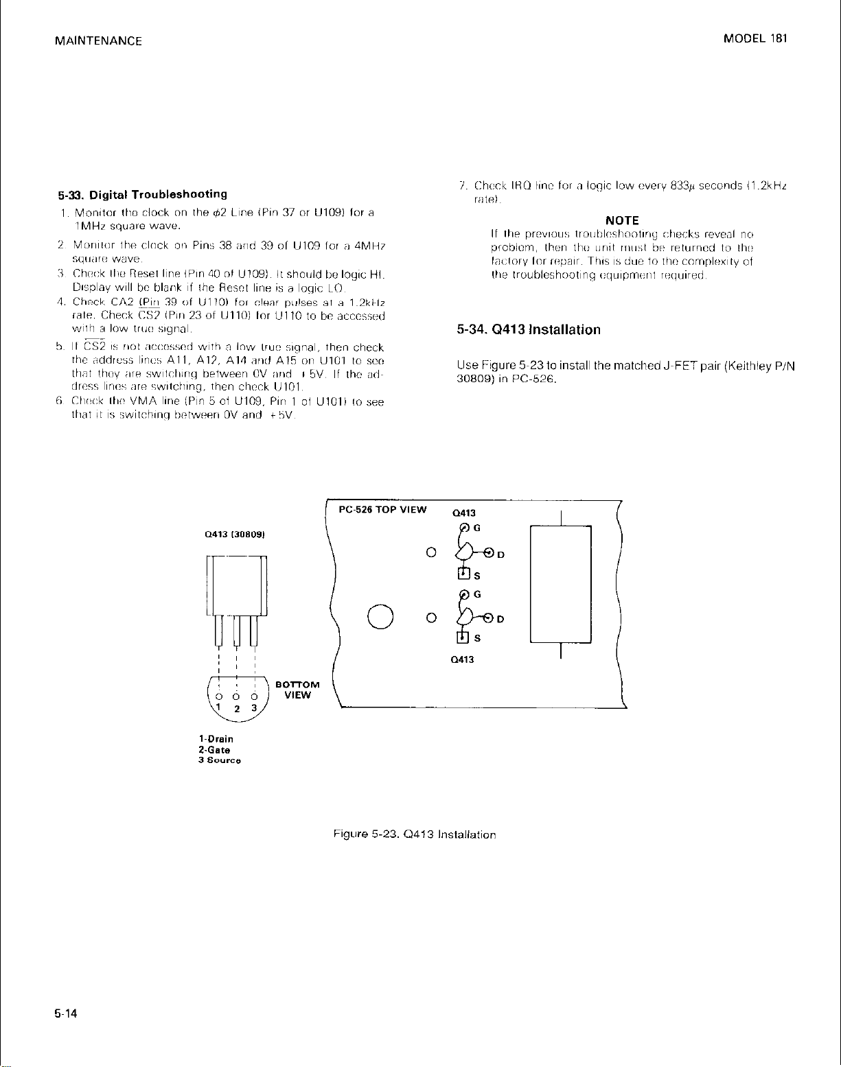
5-34. (2413 Installation
Use Figure 5~23 lo install the matched J-FET pair (Keithley P/N
308091 in PC~526.
5-14
Figure 5-23. Q413 Installation
Page 42

I
MODEL 181
REPLACEABLE PARTS
Section 6. Replaceable Parts
6-l. GENERAL
This section contains information for ordering replacement
parts. The Replaceable Parts List is arranged in alphabewal
order of the circuit designations of ihe components. Across-
reference list of manufacturers conlaining their addresses IS
given in Table 6~1.
6-2. Ordering Information
Toplacean order or lo obtain information concerning repiace~
ment parfscontactyour Keithley representativeor rhe factory.
See the inside front cover for addresses. When oiderlng.
include the following information:
A, Instrument Model Number
8. Instrument Serial Number
C. Part Description
D, Circuit Deslgnatlon (if applicable)
E. Keithley Parr Number
6-3. Factory Service
Circuit
Desig.
AT-101
AT-102
AT-103
AT-104
AT-105
C-101
c-102
c-103
c-104
Description
Opt0 Isolator
Opt0 Isolator
Opt0 Isolator
opt0 Isolator
Opt0 isolator
.l!JF. lb”, cer0
.luF, 16V, CerD
.luF, 16V. CerD
.l,,F, 16V, CerO
TABLE 6 -1
Replaceable Parts List
PC-531 - Schematic 305830
Schematic
Location
E2
E3
E4
E4
16
85'
05'
E61
A5l
PC-Board
Item No.lLocation
195/o*
196/02
197m3
198,“3
199,03
4fA3
5/A2
6102
I/C2
nfr.
Code
MOT
MOT
MOT
MOT
MOT
CLR
CLB
CLR
CLB
Mfr.
Desig.
MOC5005
HOC5005
MOCS005
MOC5005
MOC5005
"K16-104
UK16-104
UKlfi-104
UK16-104
Keithley
Part NO.
IC-292
it-292
IC-292
IC-292
IC-292
C-23G.l
C-238-.1
C-238-.1
C-238-.1
c-105
C-106
c-107
C-108
c-109
c-110
c-111
.006&F, 5OOV, CerD
22pF. 1OOOV. CerD
22pF, IOOOV, CerD
.luF, 16V, CerO
.l.F, 16V, CerD
390pF, 5OOV, CerD
.I,,F, 16V, CerD
E5'
R41
841
821
031
65
E2l
3fC2
9lC2
lOlC2
11,82
12182
13lC4
14/02
SK
CLR
CLR
CLR
CLR
CLR
CLR
5HGAD68
00220
1)11220
UK,6-104
UKlh-104
DO391
"K16-104
C-22..""6R
C-64-22pF
C-64-22pF
C-23%.1
C-23&.1
C-22-390pF
C-23%.1
Page 43

I
REPLACEABLEPARTS
MODEL 18,
TABLE 6-l
Replaceable Parts List
PC-531 - Schematic 305830
(Continued)
Circuit
Oesig.
c-112
c-113 .l!JF, 16V, tern
c-114
C-115 .luF, 16V, CerD
C-116 .lpF. 16V. Cer" G4' 19/1)2 CLR
c-117 .luF, 16V, CerO
C-118
c-119 68PF, 1ooov, CWO F41 22103 CLB DO-680 C-64.6RpF
c-120
C-121 .,pF, 16V, CerO
c-122 .l,,F, 16V, CerD F5l 25lE3 CLB UK16-104 C-238-.1
c-123 6.BuF. 25V, Electro 02 26lE2 NlC 25UKB6RROM
C-124
c-125 15OOuF, 25V, Electra
C-126 1500uF, 25V. Electra Cl 29lF2 NIC 25ULA1500 c-314-1500
Description
.lpF, 16V, cero
.luF, 10, h-D
.luF, 16V, CerO
47pF, lOOOV, CerD F51 23/03
15OOuF, 29, Electra c2
Schematic PC-Board
Location Item N&/Location Code Oesig. Part No.
E2l
E4l 16103 CLB UK16-104
E4'
F6l lR/O3
G5l
F3'
F4'
Cl
15/02 CLR
17,"3
20/E2 CLB
2l/E3 CLR
24/04 CLR
2?/F2
28lE2
Mfr. Mfr. Keithley
UK16-104 C-23-.1
C-23*-.1
CLR
CLR
ERI Type 83X
NIC 251lLA15""
NIC
UK16-104 C-23&.1
,X16-104 C-23&.1
UK16-104 C-238-.1
UK16-104 C-238-.1
UK16-104 C-238-.1
C-64.47pF
UK16-104 C-23R-.I
C-314-6.8
c-314-1500
25ULA1500 c-314-1500
C-127 K.&F, 25V, Electra
C-128 6.&F, 25V, Electra D2 31/F3 NIC 25UKB6RRUM C-314-6.8
c-129 22OOpF. 5OOV. CerD
c-130 lO,OOOuF, IOV, Electra C4 33,F3
c-131 .OZuF, 5OOV, CerD A4 34/G2
C-132
c-133 6.&F, 25V, Electra 03 36/F4
c-134
c-135
C-136
c-137
C-138
c-139 47OpF. ZOOOV, Cer"
c-140 68OPF. 2ooov, CWD
CR-101 Diode
CR-104
6.&F, 25V, Electra 03 35lF4
IOOuF, 35V, Electra c3 37IF4 NIC 35ULAlOO
IOOuF, 35V, Electra c3 38lG4
.I,,F, 16V, k-0
IuF, 5OV, Polycarb 05
IuF, 2OV, Tant Cl'
Rectifier Bridqe
"1 30/E3
--
G2 4O/F4
03 45/03
03
fl4
B4
32/F4
41lC4 EC, 625BIA105 C-215-1
42/R2 SIE
46fD3
E4
53IF4
NIC 25UKR6RRDM C-314-6.X
ERI
NIC 1nuP1n.000 c-304-10.000
ERI TYPE811 c-22-.02
NIC 25UKB6RRD17 C-314-6.8
NIC 25UKB6R8017 C-314-6.8
NIC 35ULAlOO c-295-1(30
CLR UK16-104 C-238-.1
AC1 470pF
ACI 6ROPF
F-I
G-I 2735
TYPE831
82lA105K020N C-204-1
lN46fl7
C-22.2200pF
c-295-100
C-324.470pF
C-324-6BOpF
RF-41
RF-48
Page 44

I
MODEL181
TABLE h-l
Replaceable Parts List
PC-531 - Schematic 305830
(Continued)
REPLACEABLE PARTS
Circuit
Oesig. Oescription
CR-105 Rectifier Rridqe
CR-106
CR-107
F-101
F-10,
JlOOl Binding Post (Red)
J1002
51003
J1004
51005
J1006
JlOll
51012 Connector
L-101
PI007
Rectifier Bridge
Rectifier Bridge
Fuse 1/4A (115V)
Fuse 1/8A (230V)
Dinding Post (Black) A2
Millivolt Input Connector A2
Binding Post (Red) n5
Binding Post (Black)
IEEE Connector
power connector
100uH Choke F4 60,03
12 Pin Connector
Schematic PC-Board
Location
Bl
B2
n3
A3
A3
Al
05
H,-H4 G4
A4
A3
Ii-H51
Item No./Location
54iF3
55,12
56/F?
_~
._
--
64105
Mfr.
Code Oeriq.
G-I W"W
G-I
L-F
L-F --
Hw' li!!
HHS 1511
AMP M$3!ilTA-ih-
HHS 1517 RP-II-1
HHS 1517 RP-11-n
AMP 552791-l cs-377
SW1 CAC-301
MOL "9-50-3031
NYT swo-10"
MOL
Mfr.
G-i W"4rl
W"4ti
313. 25" Ftl-,,
11%h39
"9-70- CS-338-12
Keithley
Part No.
11.46
li -46
9r-46
ii,-20
"P-l! -1
iiP-!! -7
':t-3wl
CXS-254
C<-287.3
CH-13
PI008
P1009
PlOlO 14 Pin Connector
P1012 3 Pin Molex Connector A3
4101
q102 NPN Silicon 06' 72105
9103 NPN Silicon
q104
q105
0106 NPN silicon C6
q107 NPN silicon C6
R-101
R-103
R-104 3.3K. 108, 1/4W, Camp
R-105
R-'OF,
Ribbon Cable Assembly
13 Pin Connector
N Channel, J FET
NPN Silicon 04
PNP Oarlington 03
3.3K, 10%. 1/4W, Camp
3.3K. 108, 1/4W, Comp
1°K Cm-met Trimer
01.Fl,ES'
HI-H5'
Hl-H51
F5' 7l/E3
n4 73IF4
"5, 06
E6
RI
Cl
C6
62lB4 K-I -- 30575A
66lE3
65132
67,FZ
74,F4
75/E3
77lE5
7RlE5
RO/B3
w/B2
R3lC3 "RN
R4,C3
R5/C4 REK
MOL
MOL
MOL
IN1
MOT
MOT
MOT 2N3904
G-E O45E1 32469-I
F-l
F-I
RRN
RRN
m-70- CS-338-13
"9-70- CS-338-14
0%65.i"3, C-288-3
ITE392 TG-128
2N3904
2N3904
2N3565 TG-39
2N3565
CR25*
CR25*
CR25*
72PMR'
TG-47
TG-47
TG-47
TG-39
TF-99
R-76-3.3K
R-76-3.X
R-76-3.3
RP-97.1°K
Page 45

REPLACEABLEPARTS
MODEL 181
TABLE h-l
Replaceable Parts List
PC-531 - Schematic 305830
Circuit Schematic PC-Board
0esiq. Description
R-107
R-108
R-109 108.8K. .I%, l/EW, MTF
R-110
R-111
R-112 lnR.RK, .l%, I/RW, MTF
R-113
R-114
R-115 lnK, 10%. 1/4W, Comp
R-116 10K. 10%. 1/4w, Camp
R-117 150n. In%, 1/4w, Comp F3
R-118
R-119 150n, 104, 1/4w, camp E4 98/03 "RN CR75* R-76-150
R-120 120n, 104, 1/4w, camp F6 991134
R-121 120n. 10%. 1/4w, Camp F2 1nnfn2 P'RN
10K Cermet Trimmer
,66.31(, .I%, l,RW, MTT R6 87lC5
4.32K, I%, l/SW. Fixed C6
392K, l%, 1/8W, Fixed C5
.I%, l,t?W. MTF
IM,
402K. 1%. IIRW, Fixed 0s
150n, 10%. 1/4W, Comp F4
Location Item No./Location Code Desiq.
Bh
86 RElC5
C6 91/c5
cc,
82 94/C2 RRN CR25* R-76.10K
"3 95,"2 RRN CR*!'* R-76.lnK
R6,C4
89lC5 "LE MFF 1 I8
on/c5 DLF MFFllR R-RR-392K
92/C!'
93/c5 "LE MFFIIR R-RR-4O?K
96102 RRN CR25* R-76-150
97/B? RRN CR25* R-76-150
Mfr. Mfr.
REK
"LE MTFl/R
.- .-
"LE CMP1,lO R-176-108.8K
",.F
"RN CR?!'* R-76-12"
72PMR*
MFFI,R R-176-,,+
CRZS*
Keithley
Part NO.
RP-97.IOK
R-176-166.X
R-176.lOR.RK
R-RR-4.32K
R-76-120
R-122 IOK, IO%, 1,4w, Camp
R-123
R-124
R-125 4.7K. IO%, 1/4W, Comp F5
R-126
R-127
R-128
R-129
R-130
R-131
R-132
R-134
s-101 Switch
S-102 Switch
s-103 Switch
ll-1Ofi Quad Z-Input Nand
,,-I"7
IOM, 10%. 114~. Camp F5 lOz?/rl3 RRN CR25* R-76-l"M
4.7K, 10%. 1/4w, coq 14 103lE3 8RN CR25* R-76.4.7K
22n. IO%, 1/4w, Camp F4 105lE4 RRN
1.x. 10%. 1/4w, Camp
IK, IO%, 1/4W, Comp 04 107/E3
InK, IO%, 1/4W, Camp E6
IK, 1%. I/ZW, MTLG
Thich Film Resistor
IM, IO%, 1/4w, Camp
3.3K, IO%, 1,4W, Corn,,
Ouad Exclusive OR
G4 1nl/n2
c4 lOhlE3 RRN CRZ* R-76.,.5K
n5 109,E5
G-4
R4 1,1/G,
E6
A3
A2 170/G2 K-i -G4
SEVI
SEV'
HRN CR25* R-76.,"K
103/a RRN CR25* R-76.4.7K
CR25* R-76-21
"RN CR?5* R-76-1K
lrlR/E5 RRN CR'??* R-76.10K
"LF CMF1,4 R-94.IK
llnlF5 RRN
RRN CR25* R-76.IM
113/C,
119/A,
12l/GS K-I -137/C?
136/C?
RRN
SHII
MOT
NAT nM74R6N
4x017
CR2S' R-76.3.3K
NE-IS/F
74Lcnn
TF-99
SW-466
SW-425
SW-377
IC-163
IC-116
Page 46

I
MODEL 181
Replaceable Parts List
PC-531 - Schematic 305830
(Continued)
REPLACEABLE PARTS
Circuit Schematic PC-Board Mfr. Nfr.
Oesig. Description Location Item No./Location Code
U-IOR mln RAM
u-109 641)X Micro Pr"cess"r RZ' 134/C?
11.110 6522 PIA c3'
U-116
U-117 Multiplyinq OAC
il-11R
u-119
u-12n R Rit Shift wqistor
11-121
U-127
u-123
u-124
11-125
U-126
U-127
U-128
U-129
u-130 -15V Regulator
u-131
U-132 Tri-state Buffer F4
u-133
u-134 Bidirectional Bus Driver
u-135
U-136 +15V Regulator c3 161,F4
Latch Tristate nutput EZ'
FET Input np Amp cs
FET input np Mm0 "S. R6' 144tc4 NAT L~F3VN
R Rit Shift Reqistor 64' 146/E? r4nT
Dual 8’“” Flip Flop G3’ 147/R?
""al 4 Bit counter
r1i~pi.3~
Dual 4 Bit counter
Quad Z-Input Nand Gate XV'
Quad Z-Input Nand Gate SEV'
+5V Regulator C2
+15v Requlator c2
IEEE Interface Chip F2
Bidirectional Rus Driver G7
5V Requlator C4
nriv"r SEV1 149/E? T-I
A5'
RS
G4l 145/F? YnT 4nw
w, lx1
G6' 15n/pi
CI 155,F3
G3 159,F5
133fC7
135lC3 SW
141/R4
1471R4
14?/C4 NAT
14lJlE1 f4nT W74L\393
151lE3 MOT 74Lwn
157,E3
153fE2
154,F3
156/E',
157,ES
158/F',
16OlF4 MOT
em
MOT
MnT 74LS174
A-" A"714,JN
T-1
T-I
MnT MC74LS"RP
MOT t4C7*n5cP
N*T LM34,Pli
SIG 79H,SC"
ml MC6R4RR
F-I
MOT MC3447,.
MOT
NnT MC 78,. 7 15CP
Oesig.
MCf,,R!"L
MChQ"7P
SW6572
LF?SlAN
4"94
74L?'4
W75497N
%74,~%" 11.717
74LS3679C
MC3447L ,C-219
MC7RL"SALP
Keithley
Part No.
LSI-6
is,-,P
LST-78
IC-747
,C-741
:r-7'49
ii.746
r-751
ic-?S!
,C-144
!C-',?
Ir-lhs
,c-163
IC-?I5
3246%
32468-Z
32468-3
iSl-14
IC-161
lC-229
IC-223
ic-17"
u-137 -15V Regulator c3
VR-In2
VR-103
!/R-l"4 5.lV Zener Diode "6 173165
w-104 Jumper
Y-101 4."MHZ Chrystal
y-102 3.R4MHZ
N1 means Page 2 of 2 of Schematic 305830.
6.2V Zener Diode 85 171/F' CMP I~4577nw "I-W
5.,V Zener "iode
Ch 177/F', MnT IN751 "Z-54
86
R3
FS
162/F4
177/R3
lR3/C?
Iwn4
*'Followed by part description.
NAT Tt432nL715 ,I--253
MnT
CTS
txw
IN751
MP"4"
UC-lH/II
"7-5s
,I- 1
CR-,'I
CR-13
Page 47

I
REPLACEABLE PARTS
:ircuit
wig.
Description
TABLE 6-2
Replaceable Parts List
PC-529 Schematic 305850
Schematic
Location
PC-Board
Item No./Location
MODEL 181
Mfr.
Code
c-301
C-302
C-303
c-304
C-305
C-306
c-307
C-308
C-309
CR-301
CR-3n2
J-1009
J-1010
K-3n1
K-302
j-301
I-302
j-303
.ohF, lznov, POlyprOp
l,iF, 5OV, Cer
.luF, 50, Cer
.luF, 5OV, Cer
l,,F, 5ov, Cer
1°F. 5OV, Cer
.luF, 5ov. Cer
3600~~. 5nnv. 5%. PalyY
1.5PF, 5ov, Cer Tube
Silicon, IOOV, lOti
Silicon, lonv, 10m4
Molex Connector R Pin
Molex Connector 12 Pin
Relay Sp DT
Relay sp "T
N-Channel JFET(to-92)
N-Channel JFET(to-92)
N-Channel JFET (to-92)
Al
C2
E3
E3
Gl
02
El
G3
G2
G6/04
H6
Gl
A5-A6
Al
R2
"2
Rl
c3
4lB3
5/c4
6lC2
7/c2
8,E4
9104
IO/D4
,I,"3
12iC3
lb/II4
17/D4
22lE4
21/E2
B7lR4
RIIIR4
26/C2
27IC3
28lB2
ST0
ERI
CLR
CL"
FRI
CR,
CLB
MAL
ERI
T-I
T-I
MOL
MOI.
P-R
P-R
NAT
NAT
NAT
104M
UK16-104
UK16-104
8121.050-651.
104M
8121.050.651.
104M
UK16-104
Trpe SK
301.000.coK(
159C
IN4148
IN414R
n9-52.3082
09-52-3122
RL-6R
RL-6X
PF-5301
PF-5301
PF-5301
I-
C-238-.1
C-238-.1
C-237-l
C-237-l
C-238-.,
C-138-36OOpF
C-282-,.SPF
RF-28
RF-28
CS-332-R
CS-332-12
RL-68
RL-68
TG-139
TG-139
TG-139
6-6
j-304
j-305
)-306
j-307
I-308
)-309
l-310
j-311
j-312
I-313
j-314
I-315
N-Channel JFET (to-92)
N-Channel JFET (to-92)
N-Channel JFET (k-92)
N-Channel JFET (to-92)
N-Channel JFET (to-92)
N-Channel JFET (k-92)
N-Channel JFET (to-92)
PNP Silicon (to-92)
NPN Silicon (k-92)
NPN Silicon (k-92)
N-Channel FET (k-92)
PNP Silicon (to-92)
03
R4
c3
"4
B5
CZ
c3
03
03
"3
E3
F2
29/R2
3niB2
31/B2
32fB2
33/R2
34183
35/C2
36lC2
37/C2
3RiC3
39lC3
4o/c3
NAT
NAT
NAT
NAT
NAT
NAT
NAT
MllT
F-I
F-I
NAT
MOT
-
PF-5301
PF-5301
PF-5301
PF-5301
PF-5301
PF-5301
PF-5301
2N3906
2N3904
2N3904
SF51192
2N3906
TG-139
TG-139
TG-139
TG-139
TG-139
TG-139
TG-139
TG-84
TG-47
TG-47
TG-128
TG-84
Page 48

MODEL181
REPLACEABLE PARTS
TABLE 6-2
Replaceable Parts List
PC-529 - Schwatic 305850
Circui
Oesig.
Q-316
Q-317
O-318
q-319
Q-320
Q-321
R-301
R-302
R-304
R-307
R-309
R-310
R-311
R-312
R-313
Description
PNP Silicon (to-921
PNP Silicon (to-92)
PNP Silicon
NPN Silicon (to-92)
NPN Transistor Package
NPN Transistor Package
ZOOK, l%, 8W, Fixed
47K. lo%, 1/4W, Comp
RZOK, 10%. 1/4W, Comp
390K, 10%. 1/4W, Camp
ZnOn, Cermet Trim7
ZOn, Cermet Trimner
lK, .I%, l/lOW, Mtf.
4.99K, .l%, l/lOW, Mtf.
Thick Film Resistor
Schematic PC-Board Mfr. Mfr.
Location
FZ
G2
G2
G3
SE"
XV
Al
R2
03
c3
A3
A3
A4
E3
SE"
tern No./Location Code Oesig.
41/c3
42/03
43/n3
44,"2
45/n3
46104
53/R3
54182
5h,R3
59/u
hl/R3
hZiN3
63lC3
h4/C3
65,R3
M"T
MOT
MOT
r-1
K-l
K-I
CA0
RRN
RRN
llRN
REK
"EK
AC1
ACI
CA"
2N3906
2N39"h
ZN39nh
ZN-3904
-_
-_
MS-2RI
CR25'
CR25'
CR25*
72PMR'
72PMR'
'JARl/l~*
VA!?,,,"'
Keithley
Part NO.
R-314
R-315
R-316
R-317
R-318
R-319
R-320
R-321
R-322
R-323
R-324
R-325
R-326
R-327
R-328
R-329
ZOK, Cermet Trimmer
ZK, Cermet Trimmer
100*, h-met Trimer
680K, 10%. IW, Comp
19.95K, .I%, 1/8W, ww
Factory Selected
Factory Selected
46K, .I%, i,DW, WW
IOK, 14, l,I(W, MTLF.
Z.ZM, IO%, 1/4W, Camp
Thick Film Resistor
33K, IO%, 1/4W, Camp
33K, lo%, 1/4W, Camp
Thick Film Resistor
2.74K. I%, IIRW, Mtf.
6.49K, 1%. 1,8W, Mtf.
n2
A2
Cl
n2
c2
0,
"1
Cl
E2
F3
SEV
C6
C5
SEV
"1
02
h6/R4
67,"4
68lC4
69/R4
7OlC4
71lC4
72/C4
731c4
74,03
75,CR
76iC2
lliC2
7RIC2
79/03
no/c4
RI/D4
"EK
REK
ORN
A-R
K-I
--
-.
KEL
RRN
CTS
RRN
RRN
CTS
OLE
"LE
-
72PMR'
IZPNR
3299w*
TYPFG"'
CR25*
CR25+
CR?,'
.FMM, l/R*
MFI, l/R*
R-295-4hY
R-RR-I"Y
R-76-2.21'
TF -RI
R-76-331
R-76.33Y
TF-45
R-88-2.14
R-RR-6.4$
Page 49

I
REPLACEABLEPARTS
TABLE 6-2
Replaceable Parts List
PC-529 - Schematic 305850
(Continued)
MODEL181
Circuit
Desig.
R-33"
R-331
R-332
R-333
R-334
R-335
R-336
R-337
R-33R
R-3311
R-340
K-34,
R-342
11-343
R-344
Description
4.64K, 1%. l/RW, Mtf.
loon, lo%, 1/4w, camp
91°K. l"R, 1,4w, camp
1M. IO%, 1/4w. camp
1M. 104, 1/4w, camp
IM, 10%. 1/4w, camp
2.7K, 10%. Il'lW, Camp
3.'vK, 1%. I/W. I~ixed
39.2K. 1%. I/iiW. Fixed
24.'IK, 1%. *,&I, FixW
2.5K, .I%, I/RW. Mtf.
32RK. .l%, l,RW, btf.
iM, 104.. 1/4w, coinp
IM. I"%, 1,nw. cnm*
l""k, Cermet Tri linler
Schematic
Location
PC-Board
Item Na./Locatior
RZ/D4
R3/04
116,"Z
Ill/R2
lIR/R?
119lR2
12OlC4
l?l,C4
122ic4
123,C4
114lC4
125ic4
126,"Z
121,"2
12il,"Z
Mfr.
Codr
"LE
RRN
RRN
"RN
"RN
I1RN
RRN
"LE
"LC
"LT
"LC
"LF
"RN
"RN
n II F1
Mfr.
oesi9.
MFF, l/R*
CR25*
CR25'
CR25*
ci125*
iX25*
CR?!,*
MrI'l,ii
MFil,*
MFFI,R
MFF, /R
Mli~l,"
CR25
CRTS
3686.,F-104
Keithley
Part No.
R-RR-4.64K
R-76-100
R-76.91°K
R-76.IM
R-76.,M
R-lh-2.7K
R-KR-3.92K
I{-RR-39,s
R-RR-24.9K
R-llh-2.w
R-176.3211K
H-76.1M
I?-,h-,M
b~P-97-lnnK
6-8
II-301
11.302
U-303
I-3"4
11-305
\I-306
11.307
11.308
11-30'1
11.3,"
11-311
"R-301
VR-302
"R-303
"R-304
Dprrdtiondl hplifier
Operational Amplifier
Qwrational Amplifier
Voltaqr Heferfnce
npwdtionnl nrnplifi~
nperati0n,31 hpiifier
Quad comparator
quad comparator
Quad Z-Input Nor Gate
Dual 'n" Flip Flop
comparator
5.1v, I"% ZEner
6.4V, 5% Zener
6.2V rener
6.U Lener
C3
L3
II
"1
"1
G3
SE"
ns. r3h
SK"
F4, G4
H3
"1
F4
"3
"3
9liC3
92ic3
93lC3
94,c4
95,c4
'ifi,"
')I,"2
'M/n7
99,"2
1110103
in1/n4
105m2
1"6,"3
1"7,C3
IORlC3
K-l
K-I
K-I
K-l
K-l
MT
NAT
NAT
SIG
MOT
NAT
MOT
SIE
"IC
DIG
.-
--
LF3S1N
!.M339
LM339
74t5n2
MC74574N
LM-II,
1N75l
1N451,
INR27A
lNR27A
30167
ifll63R
30154A
2~vlhR
3"154A
lC-17h
,c-214
IC-219
IC-I79
IC-216
IC-173
"7.5')
"i-61,
DZ-4H
"7.4R
Page 50

MODEL 181
REPLACEABLEPARTS
TABLE 6-3
Replaceable Parts List
PC-526 Schematic 30586D
Circuit
Desig.
0401
C402
c403
c404
c405
C406
c407
C408
c409
c410
c411
C412
c413
c414
c415
C416
c417
Description
.luF,16V, CerD
.luF, 16V, CerD
,047uF. 1oov. Polyprop
.5uF, 5OV, Polycarb
510pF. 500V. Polysty
.047uF. IOOV, Poiyprop
.047uF. lOOV, Polyprop
.015uF. ZOOV, Polycarb
.015uF, 2OOV. Polycarb
lOuF, ZOV, Tan
IOuF. ZOV. Tan
IOuF, ZOV. Tan
lOuF, 2OV. Tan
.iuF, 16V, Ceramic
.luF, 16V, Ceramic
22pF, 5OOV. Polysty
5OOOpF. 5OOV, Polysiy
Keithley
Part No.
C-238-.1
C~238~.1
C-306-.047
C.201~.5
C-138~510pF
C-306-.047
C-306-.047
C~221~.015
C.221~.015
c-179-10
c-179-10
C-179~10
C~l79.10
C~238-.1
C-238.. 1
C~, 38~22pF
C-l 38.5000pF
CR401
CR402
CR403
CR406
CR407
J1007
K401
Cl401
Q402
a403
Q404
Q405
Diode
Diode
Diode
Diode, Current Regulator
Diode, Current Regulator
12 Pin Connector
R&iY
NPN Silicon
PNP Silicon
N, Channel J-FET
N, Channel J-FET
N, Channel FET
RF~28
RF~28
RF-28
TG-140
TG~l40
cs-337-12
RL~59
TG-47
TG-84
TG-139
TG-139
TG-128
6-9
Page 51

I
MODEL if31
REPLACEABLEPARTS
TABLE 6-3
Replaceable Parts List
PC526 Schematic 30566D
(Continued)
:ircuit
ksig.
1406
1407
1408
3409
3412
2413
3414
1415
3416
3417
1418
1419
2420
R401
R402
R403
R404
R405
R406
R407
R409
R410
I?41 1
R412
R413
R414
R415
R416
R417
R418
R419
R420
Description
N, Channel FET
N, Channel FET
NPN. Silicon
N Channel J-FET
NPN Monolithic Pair
Matched J-FETS
NPN Silicon
N Channel FET
N Channel FET
N Channel FET
N Channel FET
N Channel FET
N Channel FET
200K, I%, l/EW, Mtf.
33K, 5% 1/4W, Comp.
22K, 5%, 1/4W, Comp.
22K, 5%, 1/4W, Comp.
33K, 5%, 1/4W, Camp.
ZOOK, l%, 1/8W. Mtf.
Thick Film
1 K, 10% Cermet Trimmer
100 ohm, IO%, Cermet Trimmer
1 K, 1 O%, Cermet Trimmer
20K, 1 O%, Cermet Trimmer
ZOOK, I%, IWW, MF
199.3K, O.i%, l/low, Mlf.
21.93K, 0.1%. l/low, Mti.
199.3K, O.i%, l/low, Mtf.
75K. 1%. l/8W, Mtf.
49.9K, 0.1% 1/8W, Mtf.
49.9K, 0.1% 1/8W, Mtf.
IOOK, 1%. 118W, Mtf.
Keilhley
Part No.
TG-128
TG-I 26
TG-47
TG-139
TG~i42
TG-141
TG-143
TG-128
TG-128
TG-128
TG~I 28
TG-I 28
TG-I 28
R-88~200K
R-76-33K
R-76.22K
R-76~2Zk
R-76.33K
R-88-ZOOK
TF-67
RP-89.1K
RP-89-100
RP-69-1 K
RP-89.20K
R-66.ZOOK
R-263-1 99.3K
R-263.21.93K
R-263.199.3K
R-66.75K
R-l 76.49.9K
R-176.49.9K
R-88.IOOK
I
6-10
Page 52

MODEL 181
REPLACEABLEPARTS
TABLE 6-3
Replaceable Palls List
PC-526 Schematic 305860
(Continued)
:ircuit
ksig.
1421
3422
1423
3424
3427
?428
3429
3430
3431
3432
3433
3434
3435
3436
J401
J402
J403
lJ404
u405
U406
Description
56.2K. 1%. 118W, Mtf.
56.2K, 1%. 118W. Mtf.
‘/ l%, 1/8W, Mtf.
*, 1% IBW, Mit.
looK, 5% 114W, Camp
IOOK, 5%, 1/4W, Comp.
ZK, O.i%, l/lOW, WW
2K,O.i%, l.lOW, WW
15K, 1% l/8, Mti.
4.99K, I%, 1/8W, Mtf.
IK, 1%. 118W. Mtf.
22.2K, 0.1% l.lOW, Mtf.
200 ohm, 0.1%. l/iOW. WW
IK ohm, l%, 2W. ww
Dual Op Amp
Quad Comparator
Quad Comparator
Selected. Int. Circuit
Dual Op Amp
Selected, Int. Circuit
Keithley
Part No.
R-8%56.2K
R-88.56.2K
R~88~’
&88-
R-76.IOOK
R-76-1 OOK
R-291.2K
R~291~2K
R~88~15K
R-88~499K
R-8%1K
R-263.22.2K
R-291 -200
R-290- 1 K
30475A
IC~219
K-219
30154
30477
30167
VR401
VR402
VR403
VR404
VR405
VR406
* Followed by part description
** Selected at factory.
Zener Diode 6.2V
Zener Diode 6.2V
Zener Diode 6.4V
Zener Diode 6.4V
Zener Diode 4.7V
Zener Diode 4.7V
DZ~48
DZ~40
DZ~60
DZ-60
DZ-67
DZ-67
Page 53

I
REPLACEABLE PARTS
TABLE 6-4
RP”,aceable Mechanica, Parts
MODEL 181
Keithley
Part No.
BOTTOM COVER
30541
Description 3uantity
Bottom Cover
30544 Tilt Bail
FA-143
Drive Pin
FE-14 FOOl
TOP
COVER
30540 Top COWI
TP-8-I Foam
617-322 Shield
FRONT PANEL
30539
30589
BP-1 1-O
BP-1 l-2
Front Panel
Front Panel Overlay
Binding Post (Black)
Binding Post (Red)
181-303-l Shield
REAR PANEL
30596
BP-1 1-o
BP-1 1-2
FH-24
FH-25
Rear Panel
Binding Post (Black)
Binding Post (Red)
Fuse Carrier Body
Fuse Carrier
MC-77 Serial No. Label
CS-254 AC Connector
1
1
1
4
1
1
1
1
1
1
1
1
1
1
1
1
1
1
1
6-12
Page 54

I
MODEL 181
REPLACEABLEPARTS
MFR.
CODE NAME AND ADDRESS
A-R
A-"
ACI
AMP Amnhenol
R"M Romar Crvstal Co.
RRN R"W"S, 1°C.
C-I Comuonents. Inc.
c R K c R K Com""nents, Inc.
CA"
CLR
Allen-Rradley Corp.
Milwaukw, WI 53204
Anal"9 "e"icPs. I"‘.
Norwood, MA 020%
American Components, Inc.
Conshohocken, PA 19423
Rroadview, IL 6",53
Middlesex, NJ "8646
Rivercide. CA 97507
"idd?f"Td. MF "4""s
Watrrtow". MA 0715*
Caddock
Riverside, CA 975"7
Centralah Division
Milwaukee, WI 5370,
cross Reference of Manufacturers
TABLE 6-5
FEDERAL
SUPPLY CODE
n1171
74355
14290
"x'h"
73,R"
80794
"675,
"9353
19647
71590
cnc
COT C"t"-C"i1 co, Inc.
cow
CTS CTS CorDoration
"LE
EC1
E",
EMC
ERI
F-I
6-E General Electric Co.
Corcom
Chicdq", IL h"h39
Providence, R, "79"s
continenta, Idirt
Warmi"ster, PA
Elkhart. IN 46514
"ale Flxtronic~
Columbus, NE 6R601
Electra-Cutle. inc.
53" Gabriel, CA 9,776
Electronic "Wia3, Inc.
Yonkers. NY 10710
EMC Industried, Inc.
Hatboro, PA 19040
Erie Technolo9ical Prod.
Erie, PA 16512
Fairchild instruments
lYo,,ntain View, CA 94043
Syracuse, NY IX?",
"5241
7,7"7
79777
7,OS"
91637
14757
83701
50417
179Rl
"7763
"3S"fi
6-13
Page 55

REPLACEABLE PARTS
MODEL 181
MFR.
CODE
RCA
RIC
SCH
T-I
NAME AN0 ADDRESS
RCA cornoration
Nashville, TN 17707
Richev
Na$hvill~, TN 37707
SchurtPr Electric Co.
Cincinnati, OH 41147
Texas ,nctrmrnts. 1°C.
“allas. TX 71231
crncc Refw~nre “f Manufactwers
TARLE e-5
FE”ERAL
SUPPLY CODE
“2714
79309
fl1791
TFL
TRW
Tr 1 ei,yne
blo,rntain viirw, Ca 94”4” 1sn1n
TRW Electric CamnonenLs IRC
R”““P, NC 28607 ,,w2
ucc united mm-CO” 1°C.
Rosemont, IL finnI
“IC “ictorcen I”*tr”me”ts co.
Cleveland, “H
Circuit
Desig.
t
L3Oi
FL101
L102
JlOll
J1012
44103
Description
Choke
(Rear
Line Filter 305831A4
Choke
Pin 305851Ai
Pin 305851A2
connector 30586
Zener Diode 30586iAl
Zener Diode 305861A2
Integrated Circuit
Integrated Circuit 305861D5
63°F’”
Table 6-6
Parts List Additions
Panel
Assembly) 30585iAi
Schematic
Dwg. No. and
Location
305831D5
30586iDi
PC Board
Item No. and
Location Part No.
Keithley
PC-529 CH~29
LF-2
PC-531:>24/G6
PC-529:129/Bi
P&529:1 30/A1
PC-526:34/C3 65-339-3
CH~29
cs-357
W-463
PC-526:120/D3 LIZ-67
PC-526:12i/D3 DZ-67
PC-526:i IO/C3 30154
PC-526:i 12iC3 30167
6-14
Page 56

Figure 6-l. Nanovolr Preamp PC-526. Component Location Diagram. Dwg~ No 30377D
Page 57

Page 58

I :
I
n
I
0
t
s
I
D
I
J
Page 59

Figure 6-4. Digital Board PC-531, Component Location Diagram Dwg. No. 30576D
Page 60

I
I
n
I
n
t
I
n
I
Page 61

Page 62

Page 63

I
I I
,
A
6 2316-24
Page 64

I
-
c
-
il
-
/ I r
!A
-I
c
-
c
--
z
2
1
O--
.
1 I
-
IL
-
4
Page 65

1
-
::
-
-
‘
-
-
6 27,6~28
Page 66

Page 67

\\,,
)-..ii
Page 68

I
MODEL 181
The IEEE section in your Model 181 may have Texas Instruments SN75160s for
U406 and U407 instead of the intended Motorola parts (MC3447s). The Texas
Instruments parts are readily identifiable by removing the top cover and
looking at the IEEE section located at the rear of the instrument. If two
chips are on a separate PC board and wired into the original sockets on
the mother board then they are the Texas Instruments SN75160s.
These parts (T.I. SN75160) DO NOT correspond to the original Schematic
309770. Everything between the 68488 chip and the connector 51006 is
different when the T.1 SN75160s are installed. The result is the same,
but the operation is accomplished differently than with the Motorola's
MC3447s. Shown on the next page is the alternate configuration for the
T.I. SN75160s.
APPENDIX A
APPENDIX A
MODEL 181 IEEE ADDENDUM
T;
ii% 36 I9 0,
iEi 35
is 34
ie 33
184 3z
iti5 3’
186 3o
Ei 29
I8 D2
” D3
I6 D4
I5 D5
I4 D6
'3
D7
‘2 DB
H
Page 69

m INSTRUMENTS
SERVICE FORM
Model No.
Serial No.
Date
Name and Telephone No.
Company
List all control settings, describe problem and check boxes that apply to problem.
q
q
Intem~ittent
q
IEEE failure
OFroot panel operational q AII ranges or functions are bad
Display or output (circle one)
aDrifts OLInable to zero
q
Unstable
q
Overload
IJCalibration only
aData required
(attach any additional sheets as necessary.)
Show a block diagram of your measurement system including all instruments connected (whether power is tumrd on or noti.
Also, describe signal source.
q
Analog output follows display
q
Obvious problem on power-up
q
Will not read applied input
UC of C required
Particular range or function had: specify
aBatteries and fuses are OK
OChecked all cables
Where is the measurement being performed? (factory, controlled laboratory, out-of-doors, etc.)
What power line voltage is used?
Relative humidity?
Any additional information. (If special modifications have been made by the user, please describe.)
Other?
Ambient Temperature’!
“F
 Loading...